ramon pallas-areny. amplifiers and signal conditioners....
TRANSCRIPT

Ramon Pallas-Areny. "Amplifiers and Signal Conditioners."
Copyright 2000 CRC Press LLC. <http://www.engnetbase.com>.

© 1999 by CRC Press LLC
Amplifiers and
Signal Conditioners
80.1 Introduction
80.2 Dynamic Range
80.3 Signal Classification
Single-Ended and Differential Signals • Narrowband and Broadband Signals • Low- and High-Output-Impedance Signals
80.4 General Amplifier Parameters
80.5 Instrumentation Amplifiers
Instrumentation Amplifiers Built from Discrete Parts • Composite Instrumentation Amplifiers
80.6 Single-Ended Signal Conditioners
80.7 Carrier Amplifiers
80.8 Lock-In Amplifiers
80.9 Isolation Amplifiers
80.10 Nonlinear Signal-Processing Techniques
Limiting and Clipping • Logarithmic Amplification • Multiplication and Division
80.11 Analog Linearization
80.12 Special-Purpose Signal Conditioners
80.1 Introduction
Signals from sensors do not usually have suitable characteristics for display, recording, transmission, orfurther processing. For example, they may lack the amplitude, power, level, or bandwidth required, orthey may carry superimposed interference that masks the desired information.
Signal conditioners,
including amplifiers, adapt sensor signals to the requirements of the receiver(circuit or equipment) to which they are to be connected. The functions to be performed by the signalconditioner derive from the nature of both the signal and the receiver. Commonly, the receiver requiresa single-ended, low-frequency (dc) voltage with low output impedance and amplitude range close to itspower-supply voltage(s). A typical receiver here is an analog-to-digital converter (ADC).
Signals from sensors can be analog or digital. Digital signals come from position encoders, switches,or oscillator-based sensors connected to frequency counters. The amplitude for digital signals must becompatible with logic levels for the digital receiver, and their edges must be fast enough to prevent anyfalse triggering. Large voltages can be attenuated by a voltage divider and slow edges can be acceleratedby a Schmitt trigger.
Analog sensors
are either self-generating or modulating.
Self-generating sensors
yield a voltage (ther-mocouples, photovoltaic, and electrochemical sensors) or current (piezo- and pyroelectric sensors) whose
Ramón Pallás-Areny
Universitat Politècnica de Catalunya

© 1999 by CRC Press LLC
bandwidth equals that of the measurand. Modulating sensors yield a variation in resistance, capacitance,self-inductance or mutual inductance, or other electrical quantities.
Modulating sensors
need to be excitedor biased (semiconductor junction-based sensors) in order to provide an output voltage or current.Impedance variation-based sensors are normally placed in voltage dividers, or in Wheatstone bridges(resistive sensors) or ac bridges (resistive and reactance-variation sensors). The bandwidth for signalsfrom modulating sensors equals that of the measured in dc-excited or biased sensors, and is twice thatof the measurand in ac-excited sensors (sidebands about the carrier frequency) (see Chapter 81). Capac-itive and inductive sensors require an ac excitation, whose frequency must be at least ten times higherthan the maximal frequency variation of the measurand. Pallás-Areny and Webster [1] give the equivalentcircuit for different sensors and analyze their interface.
Current signals can be converted into voltage signals by inserting a series resistor into the circuit.Graeme [2] analyzes current-to-voltage converters for photodiodes, applicable to other sources. Hence-forth, we will refer to voltage signals to analyze transformations to be performed by signal conditioners.
80.2 Dynamic Range
The
dynamic range
for a measurand is the quotient between the measurement range and the desiredresolution. Any stage for processing the signal form a sensor must have a dynamic range equal to or largerthan that of the measurand. For example, to measure a temperature from 0 to 100
°
C with 0.1
°
C resolution,we need a dynamic range of at least (100 – 0)/0.1 = 1000 (60 dB). Hence a 10-bit ADC should be appropriate
to digitize the signal because 2
10
= 1024. Let us assume we have a 10-bit ADC whose input range is 0 to 10V; its resolution will be 10 V/1024 = 9.8 mV. If the sensor sensitivity is 10 mV/
°
C and we connect it to theADC, the 9.8 mV resolution for the ADC will result in a 9.8 mV/(10 mV/
°
C) = 0.98
°
C resolution! In spiteof having the suitable dynamic range, we do not achieve the desired resolution in temperature because theoutput range of our sensor (0 to 1 V) does not match the input range for the ADC (0 to 10 V).
The basic function of voltage amplifiers is to amplify the input signal so that its output extends acrossthe input range of the subsequent stage. In the above example, an amplifier with a gain of 10 wouldmatch the sensor output range to the ADC input range. In addition, the output of the amplifier shoulddepend only on the input signal, and the signal source should not be disturbed when connecting theamplifier. These requirements can be fulfilled by choosing the appropriate amplifier depending on thecharacteristics of the input signal.
80.3 Signal Classification
Signals can be classified according to their amplitude level, the relationship between their source terminalsand ground, their bandwidth, and the value of their output impedance. Signals lower than around 100 mVare considered to be low level and need amplification. Larger signals may also need amplificationdepending on the input range of the receiver.
Single-Ended and Differential Signals
A
single-ended signal
source has one of its two output terminals at a constant voltage. For example,
Figure 80.1a shows a voltage divider whose terminal L remains at the power-supply reference voltageregardless of the sensor resistance, as shown in Figure 80.1b. If terminal L is at ground potential (groundedpower supply in Figure 80.1a), then the signal is single ended and grounded. If terminal L is isolatedfrom ground (for example, if the power supply is a battery), then the signal is single ended and floating.If terminal L is at a constant voltage with respect to ground, then the signal is single ended and drivenoff ground. The voltage at terminal H will be the sum of the signal plus the off-ground voltage. Therefore,the off-ground voltage is common to H and L; hence, it is called the
common-mode voltage.
For example,a thermocouple bonded to a power transistor provides a signal whose amplitude depends on the tem-perature of the transistor case, riding on a common-mode voltage equal to the case voltage.

© 1999 by CRC Press LLC
A
differential signal
source has two output terminals whose voltages change simultaneously by thesame magnitude but in opposite directions. The Wheatstone bridge in Figure 80.1c provides a differentialsignal. Its equivalent circuit (Figure 80.1d) shows that there is a differential voltage (
v
d
=
v
H
–
v
L
)proportional to
x
and a common-mode voltage (
V
c
=
V
/2) that does not carry any information about
x
. Further, the two output impedances are balanced. We thus have a balanced differential signal with asuperimposed common-mode voltage. Were the output impedances different, the signal would be unbal-anced. If the bridge power supply is grounded, then the differential signal will be grounded; otherwise,it will be floating. When the differential signal is very small as compared with the common-mode voltage,in order to simplify circuit analysis it is common to use the equivalent circuit in Figure 80.1e. Somedifferential signals (grounded or floating) do not bear any common-mode voltage.
FIGURE 80.1
Classes of signals according to their source terminals. A voltage divider (a) provides a single-endedsignal (b) where terminal L is at a constant voltage. A Wheatstone bridge with four sensors (c) provides a balanced
differential signal which is the difference between two voltages
v
H
and
v
L
having the same amplitude but oppositesigns and riding on a common-mode voltage
V
c
. For differential signals much smaller than the common-modevoltage, the equivalent circuit in (e) is used. If the reference point is grounded, the signal (single-ended or differential)will be grounded; if the reference point is floating, the signal will also be floating.
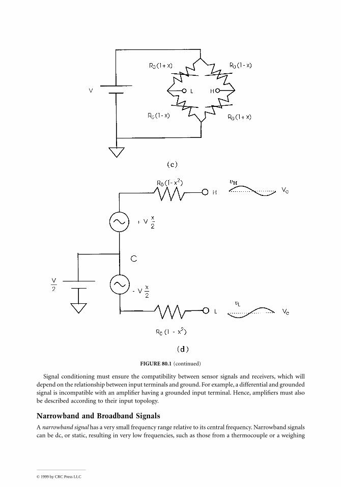
© 1999 by CRC Press LLC
Signal conditioning must ensure the compatibility between sensor signals and receivers, which willdepend on the relationship between input terminals and ground. For example, a differential and groundedsignal is incompatible with an amplifier having a grounded input terminal. Hence, amplifiers must alsobe described according to their input topology.
Narrowband and Broadband Signals
A
narrowband signal
has a very small frequency range relative to its central frequency. Narrowband signalscan be dc, or static, resulting in very low frequencies, such as those from a thermocouple or a weighing
FIGURE 80.1
(continued)

© 1999 by CRC Press LLC
scale, or ac, such as those from an ac-driven modulating sensor, in which case the exciting frequency(carrier) becomes the central frequency (see Chapter 81).
Broadband signals,
such as those from sound and vibration sensors, have a large frequency rangerelative to their central frequency. Therefore, the value of the central frequency is crucial; a signal rangingfrom 1 Hz to 10 kHz is a broadband instrumentation signal, but two 10 kHz sidebands around 1 MHzare considered to be a narrowband signal. Signal conditioning of ac narrowband signals is easier becausethe conditioner performance only needs to be guaranteed with regard to the carrier frequency.
Low- and High-Output-Impedance Signals
The output impedance of signals determines the requirements of the input impedance of the signalconditioner. Figure 80.2a shows a voltage signal connected to a device whose input impedance is
Z
d
. Thevoltage detected will be
(80.1)
Therefore, the voltage detected will equal the signal voltage only when
Z
d
>>
Z
s
; otherwise
v
d
¹
v
s
andthere will be a
loading effect.
Furthermore, it may happen that a low
Z
d
disturbs the sensor, changing thevalue of
v
s
and rendering the measurement useless or, worse still, damaging the sensor.At low frequencies, it is relatively easy to achieve large input impedances even for high-output-
impedance signals, such as those from piezoelectric sensors. At high frequencies, however, stray inputcapacitances make it more difficult. For narrowband signals this is not a problem because the value for
Z
s
and
Z
d
will be almost constant and any attenuation because of a loading effect can be taken intoaccount later. However, if the impedance seen by broadband signals is frequency dependent, then eachfrequency signal undergoes different attenuations which are impossible to compensate for.
Signals with very high output impedance are better modeled as current sources, Figure 80.2b. Thecurrent through the detector will be
FIGURE 80.1
(continued)
v vZ
Z Zd sd
d s
=+

© 1999 by CRC Press LLC
(80.2)
In order for
i
d
=
i
s
, it is required that
Z
d
<<
Z
s
which is easier to achieve than
Z
d
>>
Z
s
. If
Z
d
is not lowenough, then there is a
shunting effect.
80.4 General Amplifier Parameters
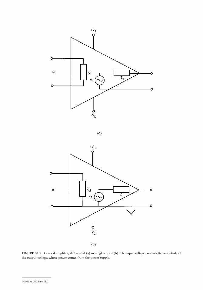
A
voltage amplifier
produces an output voltage which is a proportional reproduction of the voltagedifference at its input terminals, regardless of any common-mode voltage and without loading the voltagesource. Figure 80.3a shows the equivalent circuit for a general (differential) amplifier. If one input terminalis connected to one output terminal as in Figure 80.3b, the amplifier is single ended; if this commonterminal is grounded, the amplifier is single ended and grounded; if the common terminal is isolatedfrom ground, the amplifier is single ended and floating. In any case, the output power comes from thepower supply, and the input signal only controls the shape of the output signal, whose amplitude isdetermined by the
amplifier gain,
defined as
FIGURE 80.2
Equivalent circuit for a voltage signal connected to a voltage detector (a) and for a current signalconnected to a current detector (b). We require
Z
d
>>
Z
o
in (a) to prevent any loading effect, and
Z
d
<<
Z
s
in (b)to prevent any shunting effect.
i iZ
Z Zd ss
d s
=+
© 1999 by CRC Press LLC
FIGURE 80.3
General amplifier, differential (a) or single ended (b). The input voltage controls the amplitude ofthe output voltage, whose power comes from the power supply.
© 1999 by CRC Press LLC
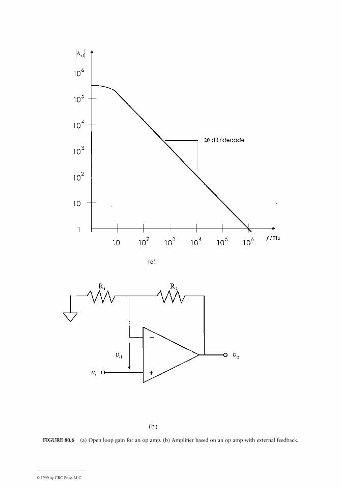
(80.3)
The ideal amplifier would have any required gain for all signal frequencies. A practical amplifier has again that rolls off at high frequency because of parasitic capacitances. In order to reduce noise and rejectinterference, it is common to add reactive components to reduce the gain for out-of-band frequenciesfurther. If the gain decreases by
n
times 10 when the frequency increases by 10, we say that the gain(downward) slope is 20
n
dB/decade. The corner (or –3 dB) frequency
f
0
for the amplifier is that for whichthe gain is 70% of that in the bandpass. (
Note:
20 log 0.7 = –3 dB). The
gain error
at
f
0
is then 30%,which is too large for many applications. If a maximal error
e
is accepted at a given frequency
f,
then thecorner frequency for the amplifier should be
(80.4)
For example,
e
= 0.01 requires
f
0
= 7
f,
e
= 0.001 requires
f
0
= 22.4
f
. A broadband signal with frequencycomponents larger than
f
would undergo amplitude distortion. A narrowband signal centered on afrequency larger than
f
would be amplified by a gain lower than expected, but if the actual gain ismeasured, the gain error can later be corrected.
Whenever the gain decreases, the output signal is delayed with respect to the output. In the aboveamplifier, an input sine wave of frequency
f
0
will result in an output sine wave delayed by 45
°
(and withrelative attenuation 30% as compared with a sine wave of frequency
f >> f0). Complex waveforms havingfrequency components close to f0 would undergo shape (or phase) distortion. In order for a waveformto be faithfully reproduced at the output, the phase delay should be either zero or proportional to thefrequency (linear phase shift). This last requirement is difficult to meet. Hence, for broadband signals itis common to design amplifiers whose bandwidth is larger than the maximal input frequency. Narrow-band signals undergo a delay which can be measured and corrected.
An ideal amplifier would have infinite input impedance. Then no input current would flow whenconnecting the signal, Figure 80.2a, and no energy would be taken from the signal source, which wouldremain undisturbed. A practical amplifier, however, will have a finite, yet large, input impedance at lowfrequencies, decreasing at larger frequencies because of stray input capacitances. If sensors are connectedto conditioners by coaxial cables with grounded shields, then the capacitance to ground can be very large(from 70 to 100 pF/m depending on the cable diameter). This capacitance can be reduced by using drivenshields (or guards) (see Chapter 89). If twisted pairs are used instead, the capacitance between wires isonly about 5 to 8 pF/m, but there is an increased risk of capacitive interference.
Signal conditioners connected to remote sensors must be protected by limiting both voltage and inputcurrents. Current can be limited by inserting a power resistor (100 W to 1 kW , 1 W for example), a PTCresistor or a fuse between each signal source lead and conditioner input. Input voltages can be limitedby connecting diodes, zeners, metal-oxide varistors, gas-discharge devices, or other surge-suppressionnonlinear devices, from each input line to dc power-supply lines or to ground, depending on the particularprotecting device. Some commercial voltage limiters are Thyzorb® and Transzorb® (General Semicon-ductor), Transil® and Trisil® (SGS-Thomson), SIOV® (Siemens), and TL7726 (Texas Instruments).
The ideal amplifier would also have zero output impedance. This would imply no loading effect becauseof a possible finite input impedance for the following stage, low output noise, and unlimited outputpower. Practical amplifiers can indeed have a low output impedance and low noise, but their outputpower is very limited. Common signal amplifiers provide at best about 40 mA output current andsometimes only 10 mA. The power gain, however, is quite noticeable, as input currents can be in thepicoampere range (10–12 A) and input voltages in the millivolt range (10–3 V); a 10 V, 10 mA outputwould mean a power gain of 1014! Yet the output power available is very small (100 mW). Power amplifiers
Gv
v= o
d
ff f
0 =-( )-
»1
2 22
e
e e e

© 1999 by CRC Press LLC
are quite the opposite; they have a relatively small power gain but provide a high-power output. For bothsignal and power amplifiers, output power comes from the power supply, not from the input signal.
Some sensor signals do not require amplification but only impedance transformation, for example, tomatch their output impedance to that of a transmission line. Amplifiers for impedance transformation(or matching) and G = 1 are called buffers.
80.5 Instrumentation Amplifiers
For instrumentation signals, the so-called instrumentation amplifier (IA) offers performance closest tothe ideal amplifier, at a moderate cost (from $1.50 up). Figure 80.4a shows the symbol for the IA andFigure 80.4b its input/output relationship; ideally this is a straight line with slope G and passing throughthe point (0,0), but actually it is an off-zero, seemingly straight line, whose slope is somewhat differentfrom G. The output voltage is
(80.5)
where va depends on the input voltage vd, the second term includes offset, drift, noise, and interference-rejection errors, G is the designed gain, and vref is the reference voltage, commonly 0 V (but not necessarily,thus allowing output level shifting). Equation 80.5 describes a worst-case situation where absolute valuesfor error sources are added. In practice, some cancellation between different error sources may happen.
Figure 80.5 shows a circuit model for error analysis when a practical IA is connected to a signal source(assumed to be differential for completeness). Impedance from each input terminal to ground (Zc) andbetween input terminals (Zd) are all finite. Furthermore, if the input terminals are both connected toground, vo is not zero and depends on G; this is modeled by Vos. If the input terminals are groundedthrough resistors, then vo also depends on the value of these resistors; this is modeled by current sourcesIB+ and IB–, which represent input bias or leakage currents. These currents need a return path, andtherefore a third lead connecting the signal source to the amplifier, or a common ground, is required.Neither Vos nor IB+ nor IB– is constant; rather, they change with temperature and time: slow changes(<0.01 Hz) are called drift and fast changes are described as noise (hence the noise sources en, in+ andin– in Figure 80.5). Common specifications for IAs are defined in Reference 3.
If a voltage vc is simultaneously applied to both inputs, then vo depends on vc and its frequency. Thecommon-mode gain is
(80.6)
In order to describe the output voltage due to vc as an input error voltage, we must divide the corre-sponding vo(vc) by G (the normal- or differential-mode gain, G = Gd). The common-mode rejectionratio (CMRR) is defined as
(80.7)
and is usually expressed in decibels ({CMRR}dB = 20 log CMRR). The input error voltage will be
(80.8)
v v v v v v G vo a os b r n ref= + + + +( ) +
G fV v
Vc
o d
c
( ) ==( )0
CMRRd
c
=( )( )
G f
G f
v v
G
G v
G
vo c
d
c c
d
c
CMRR
( )= =

© 1999 by CRC Press LLC
In the above analysis we have assumed Zc << Ro; otherwise, if there were any unbalance (such as thatfor the source impedance in Figure 80.5), vc at the voltage source would result in a differential-modevoltage at the amplifier input,
(80.9)
FIGURE 80.4 Instrumentation amplifier. (a) Symbol. (b) Ideal and actual input/output relationship. The idealresponse is a straight line through the point (0,0) and slope G.
v v vR R
Z R R
R
Z Rd c co o
c o o
o
c o
( ) = ++ +
-+
æ
èçö
ø÷D
D

© 1999 by CRC Press LLC
which would be amplified by Gd. Then, the effective common-mode rejection ratio would be
(80.10)
where the CMRR is that of the IA alone, expressed as a fraction, not in decibels. Stray capacitances frominput terminals to ground will decrease Zc, therefore reducing CMRRe.
The ideal amplifier is unaffected by power supply fluctuations. The practical amplifier shows outputfluctuations when supply voltages change. For slow changes, the equivalent input error can be expressedas a change in input offset voltages in terms of the power supply rejection ratio (PSRR),
(80.11)
The terms in Equation 80.5 can be detailed as follows. Because of gain errors we have
(80.12)
where G is the differential gain designed, eG its absolute error, DG/DT its thermal drift, DT the differencebetween the actual temperature and that at which the gain G is specified, and eNLG is the nonlinearitygain error, which describes the extent to which the input/output relationship deviates from a straight
FIGURE 80.5 A model for a practical instrumentation amplifier including major error sources.
vZ R
Z R R Z Rv
R
Zcc o
c o o c o
co
c
=+ +( ) +( ) »D
DD
1 1
CMRR CMRRe
o
c
= +DR
Z
PSRR os
s
= DDV
V
v v G eG
TT ea d G NLG= + + ´ +
æ
èçö
ø÷DD
D

© 1999 by CRC Press LLC
line (insert in Figure 80.4b). The actual temperature TJ is calculated by adding to the current ambienttemperature TA the temperature rise produced by the power PD dissipated in the device. This rise dependson the thermal resistance qJA for the case
(80.13)
where PD can be calculated from the respective voltage and current supplies
(80.14)
The terms for the equivalent input offset error will be
(80.15)
(80.16)
where Ta is the ambient temperature in data sheets, Ios = IB+ – IB– is the offset current, IB = (IB+ + IB–)/2,and all input currents must be calculated at the actual temperature,
(80.17)
Error contributions from finite interference rejection are
(80.18)
where the CMRRe must be that at the frequency for vc, and the PSRR must be that for the frequency ofthe ripple DVs . It is assumed that both frequencies fall inside the bandpass for the signal of interest vd.
The equivalent input voltage noise is
(80.19)
where en2 is the voltage noise power spectral density of the IA, in+
2 and in–2 are the current noise power
spectral densities for each input of the IA, and Be, Bi+, and Bi– are the respective noise equivalentbandwidths of each noise source. In Figure 80.5, the transfer function for each noise source is the sameas that of the signal vd. If the signal bandwidth is determined as fh – f1 by sharp filters, then
(80.20)
(80.21)
where fce and fci are, respectively, the frequencies where the value of voltage and current noise spectraldensities is twice their value at high frequency, also known as corner or 3 dB frequencies.
T T PJ A D JA= + ´ q
P V I V ID S+ S+ S S= + - -
v V TV
TT Tos os a
osJ a= ( ) + ´ -( )D
D
v I I R I R I R I Rb B+ B o B+ o os o B o= -( ) + = +- D D
I I TI
TT T= ( ) + ´ -( )a J a
DD
vv V
rc
e
s
CMRR PSRR= + D
v e B i R B i R Bn n2
e n2
o2
i+ n2
o2
i–= + - + -
B f f ff
fe h 1 ceh
1
= - + ln
B B f f ff
fi+ i– h 1 cih
1
= = - + ln

© 1999 by CRC Press LLC
Another noise specification method states the peak-to-peak noise at a given low-frequency band (fA tofB), usually 0.1 to 10 Hz, and the noise spectral density at a frequency at which it is already constant,normally 1 or 10 kHz. In these cases, if the contribution from noise currents is negligible, the equivalentinput voltage noise can be calculated from
(80.22)
where vnL and vnH are, respectively, the voltage noise in the low-frequency and high-frequency bandsexpressed in the same units (peak-to-peak or rms voltages). To convert rms voltages into peak-to-peakvalues, multiply by 6.6. If the signal bandwidth is from f1 to fh, and f1 = fA and fh > fB, then Equation 80.22can be written
(80.23)
where vnL is the peak-to-peak value and en is the rms voltage noise as specified in data books.Equation 80.23 results in a peak-to-peak calculated noise that is lower than the real noise, because noisespectral density is not constant from fB up. However, it is a simple approach providing useful results.
For signal sources with high output resistors, thermal and excess noise from resistors (see Chapter 54)must be included. For first- and second-order filters, noise bandwidth is slightly larger than signalbandwidth. Motchenbacher and Connelly [4] show how to calculate noise bandwidth, resistor noise, andnoise transfer functions when different from signal transfer functions.
Low-noise design always seeks the minimal bandwidth required for the signal. When amplifying low-frequency signals, if a large capacitor Ci is connected across the input terminals in Figure 80.5, then noiseand interference having a frequency larger than f0 = 1/2p(2Ro)Ci (f0 << fs) will be attenuated.
Another possible source of error for any IA, not included in Equation 80.5, is the slew rate limit of itsoutput stage. Because of the limited current available, the voltage at the output terminal cannot changefaster than a specified value SR. Then, if the maximal amplitude A of an output sine wave of frequency fexceeds
(80.24)
there will be a waveform distortion.Table 80.1 lists some basic specifications for IC instrumentation amplifies whose gain G can be set by
an external resistor or a single connection.
Instrumentation Amplifiers Built from Discrete Parts
Instrumentation amplifiers can be built from discrete parts by using operational amplifiers (op amps)and a few resistors. An op amp is basically a differential voltage amplifier whose gain Ad is very large(from 105 to 107) at dc and rolls off (20 dB/decade) from frequencies of about 1 to 100 Hz, becoming 1at frequencies from 1 to 10 MHz for common models (Figure 80.6a), and whose input impedances areso high (up to 1012 W * * 1 pF) that input currents are almost negligible. Op amps can also be modeledby the circuit in Figure 80.5, and their symbol is that in Figure 80.4a, deleting IA. However, because oftheir large gain, op amps cannot be used directly as amplifiers; a mere 1 mV dc input voltage wouldsaturate any op amp output. Furthermore, op amp gain changes from unit to unit, even for the samemodel, and for a given unit it changes with time, temperature, and supply voltages. Nevertheless, byproviding external feedback, op amps are very flexible and far cheaper than IAs. But when the cost forexternal components and their connections, and overall reliability are also considered, the optimalsolution depends on the situation.
v v vn nL2
nH2= +
v v e f fn nL2
n h B= + ( ) -( )6 62
.
Af
=p
SR
2

© 1999 by CRC Press LLC
TABLE 80.1 Basic Specifications for Some Instrumentation Amplifiers
AD624A AMP02F INA110KP LT1101AC Units
Gain range 1–1000 1–1000 1–500 10,100 V/VGain error, eG
G = 1 ±0.05 0.05 ±0.02 n.a. %G = 10 n.s. 0.40 ±0.05 ±0.04 %G = 100 ±0.25 0.50 ±0.10 ±0.04 %G = 1000 ±1.0 0.70 n.a. n.a. %
Gain nonlinearity error eNLGa
G = 1 ±0.005 0.006 ±0.005 n.a. %G = 10 n.s. 0.006 ±0.005 ±0.0008 %G = 100 ±0.005 0.006 ±0.01 ±0.0008G = 1000 ±0.005 0.006 n.a. n.a. %
Gain drift DG/DTG = 1 5 50 ±10 n.a. mV/V/°CG = 10 n.s. 50 ±10 5 mV/V/°CG = 100 10 50 ±20 5 mV/V/°CG = 1000 25 50 n.a. n.a. mV/V/°C
Vos 200 + 5/G 200 ±(1000 + 5000/G) 160 mVDvos/DT 2 + 50/G 4 ±(2 + 50/G) 2 mV/°CIB ±50 20 0.05 10 nADIB/DT ±50 typ 250 typ b 30 pA/°CIos ±35 10 0.025 0.90 nADIos/DT ±20 typ 15 typ n.s. 7.0 pA/°CZd 1 ** 10 typ 10 typ 5000 ** 6 typ 12 GWZc 1 ** 10 typ 16.5 typ 2000 ** 1 typ 7 GWCMRR at dc
G = 1 70 min 80 min 70 min n.a. dBG = 10 n.s. 100 min 87 min 82 dBG = 100 100 min 115 min 100 min 98 dBG = 1000 110 min 115 min n.a. n.a. dB
PSRR at dcG = 1 70 min 80 min c n.a. dBG = 10 n.s. 100 min c 100 dBG = 100 95 min 115 min c 100 dBG = 1000 100 min 115 min n.a. n.a. dB
Bandwidth (–3 dB) (typ)G = 1 1000 1200 2500 n.a. kHzG = 10 n.s. 300 2500 37 kHzG = 100 150 200 470 3.5 kHzG = 1000 25 200 n.a. n.a. kHz
Slew rate (typ) 5.0 6 17 0.1 V/msSettling time to 0.01%
G = 1 15 typ 10 typ 12.5 n.a. msG = 10 15 typ 10 typ 7.5 n.a. msG = 100 15 typ 10 typ 7.5 n.a. msG = 1000 75 typ 10 typ n.a. n.a. ms
en (typ)
G = 1 4 120 66 n.a. nV/
G = 10 4 18 12 43 nV/
G = 100 4 10 10 43 nV/
G = 1000 4 9 n.a. n.a. nV/vn 0.1 to 10 Hz (typ)
G = 1 10 10 1 0.9 mVp-pG = 10 n.s. 1.2 1 0.9 mVp-pG = 100 0.3 0.5 1 0.9 mVp-pG = 1000 0.2 0.4 1 0.9 mVp-p
Hz
Hz
Hz
Hz

© 1999 by CRC Press LLC
Figure 80.6b shows an amplifier built from an op amp with external feedback. If input currents areneglected, the current through R2 will flow through R1 and we have
(80.25)
(80.26)
Therefore,
(80.27)
where Gi = 1 + R2/R1 is the ideal gain for the amplifier. If Gi/Ad is small enough (Gi small, Ad large), thegain does not depend on Ad but only on external components. At high frequencies, however, Ad becomessmaller and, from Equation 80.27, vo < Givs so that the bandwidth for the amplifier will reduce for largegains. Franco [5] analyzes different op amp circuits useful for signal conditioning.
Figure 80.7 shows an IA built from three op amps. The input stage is fully differential and the outputstage is a difference amplifier converting a differential voltage into a single-ended output voltage. Differenceamplifiers (op amp and matched resistors) are available in IC form: AMP 03 (Analog Devices) and INA105/6 and INA 117 (Burr-Brown). The gain equation for the complete IA is
(80.28)
Pallás-Areny and Webster [6] have analyzed matching conditions in order to achieve a high CMRR.Resistors R2 do not need to be matched. Resistors R3 and R4 need to be closely matched. A potentiometerconnected to the vref terminal makes it possible to trim the CMRR at low frequencies.
The three-op-amp IA has a symmetrical structure making it easy to design and test. IAs based on anIC difference amplifier do not need any user trim for high CMRR. The circuit in Figure 80.8 is an IAthat lacks these advantages but uses only two op amps. Its gain equation is
in 0.1 to 10 Hz (typ) 60 n.s. n.s. 2.3 pAp-p
in (typ) n.s. 400 1.8 20 fA/
Note: All parameter values are maximum, unless otherwise stated (typ = typical; min = minimum; n.a. =not applicable; n.s. = not specified). Measurement conditions are similar; consult manufacturers’ data booksfor further detail.
a For the INA110, the gain nonlinearity error is specified as percentage of the full-scale output.b Input current drift for the INA110KP approximately doubles for every 10°C increase, from 25°C (10 pA-
typ) to 125°C (10 nA-typ).c The PSRR for the INA110 is specified as an input offset ±(10 + 180/G) mV/V maximum.
TABLE 80.1 (continued) Basic Specifications for Some Instrumentation Amplifiers
AD624A AMP02F INA110KP LT1101AC Units
Hz
v v vR
R Rd s o1= -
+1 2
v A vo d d=
v
v
AR
R
AR
R
G
G
A
o
s
d
d
i
i
d
=+
æ
èçö
ø÷
+ +=
+
1
1 1
2
1
2
1
GR
R
R
R= +
æ
èçö
ø÷1 2 2
1
4
3
© 1999 by CRC Press LLC
FIGURE 80.6 (a) Open loop gain for an op amp. (b) Amplifier based on an op amp with external feedback.

© 1999 by CRC Press LLC
FIGURE 80.7 Instrumentation amplifier built from three op amps. R3 and R4 must be matched.
FIGURE 80.8 Instrumentation amplifier built from two op amps. R1 and R2 must be matched.
© 1999 by CRC Press LLC
80.12 Special-Purpose Signal Conditioners
Table 80.4 lists some signal conditioners in IC form intended for specific sensors and describes theirrespective functions. The decision whether to design a signal conditioner from parts or use a model fromTable 80.4 is a matter of cost, reliability, and availability. Signal conditioners are also available as sub-systems (plug-in cards and modules), for example, series MB from Keithley Metrabyte, SCM from Burr-Brown, and 3B, 5B, 6B, and 7B from Analog Devices.
Defining Terms
Carrier amplifier: Voltage amplifier for narrowband ac signals, that includes in addition a sine waveoscillator, a synchronous demodulator, and a low-pass filter.
Common-mode rejection ratio (CMRR): The gain for a differential voltage divided by the gain for acommon-mode voltage in a differential amplifier. It is usually expressed in decibels.
Common-mode voltage: The average of the voltages at the input terminals of a differential amplifier.Differential amplifier: Circuit or device that amplifies the difference in voltage between two terminals,
none of which is grounded.Dynamic range: The measurement range for a quantity divided by the desired resolution.Instrumentation amplifier: Differential amplifier with large input impedance and low offset and gain
errors.Isolation amplifier: Voltage amplifier whose ground terminal for input voltages is independent from
the ground terminal for the output voltage (i.e., there is a large impedance between both groundterminals).
Isolation Mode Rejection Ratio (IMRR): The amplitude of the output voltage of an isolation amplifierdivided by the voltage across the isolation impedance yielding that voltage.
Signal conditioner: Circuit or device that adapts a sensor signal to an ensuing circuit, such as an analog-to-digital converter.
Voltage buffer: Voltage amplifier whose gain is 1, or close to 1, and whose input impedance is verylarge while its output impedance is very small.
TABLE 80.4 Special-Purpose Integrated Circuit Signal Conditioners
Model Function Manufacturer
4341 rms-to-dc converter Burr-BrownACF2101 Low-noise switched integrator Burr-BrownAD1B60 Intelligent digitizing signal conditioner Analog DevicesAD2S93 LVDT-to-digital converter (ac bridge conditioner) Analog DevicesAD594 Thermocouple amplifier with cold junction compensation Analog DevicesAD596/7 Thermocouple conditioner and set-point controllers Analog DevicesAD598 LVDT signal conditioner Analog DevicesAD636 rms-to-dc (rms-to-dc converter) Analog DevicesAD670 Signal conditioning ADC Analog DevicesAD698 LVDT signal conditioner Analog DevicesAD7710 Signal conditioning ADC with RTD excitation currents Analog DevicesAD7711 Signal conditioning ADC with RTD excitation currents Analog DevicesIMP50E10 Electrically programmable analog circuit IMPLM903 Fluid level detector National SemiconductorLM1042 Fluid level detector National SemiconductorLM1819 Air-core meter driver National SemiconductorLM1830 Fluid detector National SemiconductorLT1025 Thermocouple cold junction compensator Linear TechnologyLT1088 Wideband rms-to-dc converter building block Linear TechnologyLTK001 Thermocouple cold junction compensator and matched amplifier Linear TechnologyTLE2425 Precision virtual ground Texas Instruments

© 1999 by CRC Press LLC
References
1. R. Pallás-Areny and J.G. Webster, Sensors and Signal Conditioning, New York: John Wiley & Sons, 1991.2. J. Graeme, Photodiode Amplifiers, Op Amp Solutions, New York: McGraw-Hill, 1996.3. C. Kitchin and L. Counts, Instrumentation Amplifier Application Guide, 2nd ed., Application Note,
Norwood, MA: Analog Devices, 1992.4. C.D. Motchenbacher and J.A. Connelly, Low-Noise Electronic System Design, New York: John
Wiley & Sons, 1993.5. S. Franco, Design with Operational Amplifiers and Analog Integrated Circuits, 2nd ed., New York:
McGraw-Hill, 1998.6. R. Pallás-Areny and J.G. Webster, Common mode rejection ratio in differential amplifiers, IEEE
Trans. Instrum. Meas., 40, 669–676, 1991.7. R. Pallás-Areny and O. Casas, A novel differential synchronous demodulator for ac signals, IEEE
Trans. Instrum. Meas., 45, 413–416, 1996.8. M.L. Meade, Lock-in Amplifiers: Principles and Applications, London: Peter Peregrinus, 1984.9. W.G. Jung, IC Op Amp Cookbook, 3rd ed., Indianapolis, IN: Howard W. Sams, 1986.
10. Y.J. Wong and W.E. Ott, Function Circuits Design and Application, New York: McGraw-Hill, 1976.11. A.J. Peyton and V. Walsh, Analog Electronics with Op Amps, Cambridge, U.K.: Cambridge University
Press, 1993.12. D.H. Sheingold, Ed., Multiplier Application Guide, Norwood, MA: Analog Devices, 1978.
Further Information
B.W.G. Newby, Electronic Signal Conditioning, Oxford, U.K.: Butterworth-Heinemann, 1994, is a bookfor those in the first year of an engineering degree. It covers analog and digital techniques at beginners’level, proposes simple exercises, and provides clear explanations supported by a minimum of equations.
P. Horowitz and W. Hill, The Art of Electronics, 2nd ed., Cambridge, U.K.: Cambridge University Press,1989. This is a highly recommended book for anyone interested in building electronic circuits withoutworrying about internal details for active components.
M.N. Horenstein, Microelectronic Circuits and Devices, 2nd ed., Englewood Cliffs, NJ: Prentice-Hall,1996, is an introductory electronics textbook for electrical or computer engineering students. It providesmany examples and proposes many more problems, for some of which solutions are offered.
J. Dostál, Operational Amplifiers, 2nd ed., Oxford, U.K.: Butterworth-Heinemann, 1993, provides agood combination of theory and practical design ideas. It includes complete tables which summarizeserrors and equivalent circuits for many op amp applications.
T.H. Wilmshurst, Signal Recovery from Noise in Electronic Instrumentation, 2nd ed., Bristol, U.K.: AdamHilger, 1990, describes various techniques for reducing noise and interference in instrumentation. Noreferences are provided and some demonstrations are rather short, but it provides insight into veryinteresting topics.
Manufacturers’ data books provide a wealth of information, albeit nonuniformly. Application notesfor special components should be consulted before undertaking any serious project. In addition, appli-cation notes provide handy solutions to difficult problems and often inspire good designs. Most manu-facturers offer such literature free of charge. The following have shown to be particularly useful and easyto obtain: 1993 Applications Reference Manual, Analog Devices; 1994 IC Applications Handbook, Burr-Brown; 1990 Linear Applications Handbook and 1993 Linear Applications Handbook Vol. II, Linear Tech-nology; 1994 Linear Application Handbook, National Semiconductor; Linear and Interface Circuit Appli-cations, Vols. 1, 2, and 3, Texas Instruments.
R. Pallás-Areny and J.G. Webster, Analog Signal Processing, New York: John Wiley & Sons, 1999, offersa design-oriented approach to processing instrumentation signals using standard analog integrated cir-cuits, that relies on signal classification, analog domain conversions, error analysis, interference rejectionand noise reduction, and highlights differential circuits.

Rahman Jamal, et. al.. "Filters."
Copyright 2000 CRC Press LLC. <http://www.engnetbase.com>.
© 1999 by CRC Press LLC
Filters
82.1 Introduction
82.2 Filter Classification
82.3 The Filter Approximation Problem
Butterworth Filters • Chebyshev Filters of Chebyshev I Filters Elliptic or Cauer Filters • Bessel Filters
82.4 Design Examples for Passive and Active Filters
Passive
R
,
L
,
C
Filter Design • Active Filter Design
82.5 Discrete-Time Filters
82.6 Digital Filter Design Process
82.7 FIR Filter Design
Windowed FIR Filters • Optimum FIR Filters • Design ofNarrowband FIR Filters
82.8 IIR Filter Design
Design of Arbitrary IIR Filters • Cascade-Form IIR FilterStructures
82.9 Wave Digital Filters
82.10 Antialiasing and Smoothing Filters
82.11 Switched Capacitor Filters
82.12 Adaptive Filters
82.1 Introduction
In its broadest sense, a filter can be defined as a signal processing system whose output signal, usuallycalled the
response
, differs from the input signal, called the
excitation
, such that the output signal hassome prescribed properties. In more practical terms an electric filter is a device designed to suppress,pass, or separate a group of signals from a mixture of signals according to the specifications in a particularapplication. The application areas of filtering are manifold, for example to band-limit signals beforesampling to reduce aliasing, to eliminate unwanted noise in communication systems, to resolve signalsinto their frequency components, to convert discrete-time signals into continuous-time signals, todemodulate signals, etc. Filters are generally classified into three broad classes:
continuous-time
,
sampled-data
, and
discrete-time
filters depending on the type of signal being processed by the filter. Therefore,the concept of signals are fundamental in the design of filters.
A
signal
is a function of one or more independent variables such as time, space, temperature, etc. thatcarries information. The independent variables of a signal can either be continuous or discrete. Assumingthat the signal is a function of time, in the first case the signal is called continuous-time and in thesecond, discrete-time. A continuous-time signal is defined at every instant of time over a given interval,whereas a discrete-time signal is defined only at a discrete-time instances. Similarly, the
values
of a signalcan also be classified in either continuous or discrete.
Rahman Jamal
National Instruments Germany
Robert Steer
Frequency Devices

© 1999 by CRC Press LLC
In real-world signals, often referred to as analog signals, both amplitude and time are continuous.These types of signals cannot be processed by digital machines unless they have been converted intodiscrete-time signals. By contrast, a digital signal is characterized by discrete signal values, that are definedonly at discrete points in time. Digital signal values are represented by a finite number of digits, whichare usually binary coded. The relationship between a continuous-time signal and the correspondingdiscrete-time signal can be expressed in the following form:
(82.1)
where
T
is called the sampling period.Filters can be classified on the basis of the input, output, and internal operating signals. A continuous
data filter is used to process continuous-time or analog signals, whereas a digital filter processes digitalsignals. Continuous data filters are further divided into
passive
or
active
filters, depending on the typeof elements used in their implementation. Perhaps the earliest type of filters known in the engineeringcommunity are
LC
filters, which can be designed by using discrete components like inductors andcapacitors, or crystal and mechanical filters that can be implemented using
LC
equivalent circuits. Sinceno external power is required to operate these filters, they are often referred to as
passive
filters. In contrast,
active
filters are based on active devices, primarily
RC
elements, and amplifiers. In a sampled data filter,on the other hand, the signal is sampled and processed at discrete instants of time. Depending on thetype of signal processed by such a filter, one may distinguish between an
analog
sampled
data
filter anda
digital
filter. In an analog sampled data filter the sampled signal can principally take any value, whereasin a digital filter the sampled signal is a digital signal, the definition of which was given earlier. Examplesof analog sampled data filters are switched capacitor (SC) filters and charge-transfer device (CTD) filtersmade of capacitors, switches, and operational amplifiers.
82.2 Filter Classification
Filters are commonly classified according to the filter function they perform. The basic functions are:low-pass, high-pass, bandpass, and bandstop. If a filter passes frequencies from zero to its cutoff frequency
W
c
and stops all frequencies higher than the cutoff frequencies, then this filter type is called an ideal
low-pass filter
. In contrast, an ideal
high-pass filter
stops all frequencies below its cutoff frequency and passesall frequencies above it. Frequencies extending from
W
1
to
W
2
are passed by an ideal
bandpass filter
,while all other frequencies are stopped. An ideal bandstop filter stops frequencies from
W
1
to
W
2
andpasses all other frequencies. Figure 82.1 depicts the magnitude functions of the four basic
ideal filter
types.So far we have discussed ideal filter characteristics having rectangular magnitude responses. These
characteristics, however, are physically not realizable. As a consequence, the ideal response can only beapproximated by some nonideal realizable system. Several classical approximation schemes have beendeveloped, each of which satisfies a different criterion of optimization. This should be taken into accountwhen comparing the performance of these filter characteristics.
82.3 The Filter Approximation Problem
Generally the input and output variables of a linear, time-invariant, causal filter can be characterizedeither in the time-domain through the convolution integral given by
(82.2)
or, equivalently, in the frequency-domain through the transfer function
x kT x t k( ) = ( ) = ¼t=kT
, , , , ,0 1 2
y t h t x t dt( ) = -( ) ( )ò a
0
t t

© 1999 by CRC Press LLC
(82.3)
where
H
a
(
s
) is the Laplace transform of the impulse response
h
a
(
t
) and
X
(
s
),
Y
(
s
) are the Laplace transformsof the input signal
x
(
t
) and the output or the filtered signal
y
(
t
).
X
(
s
) and
Y
(
s
) are polynomials in
s
=
s
+
j
W
and the overall transfer function
H
a
(
s
) is a real rational function of
s
with real coefficients. Thezeroes of the polynomial
X
(
s
) given by
s
=
s
¥
i
are called the poles of
H
a
(
s
) and are commonly referred toas the
natural
frequencies
of the filter. The zeros of
Y
(
s
) given by
s
=
s
0i
which are equivalent to the zeroesof
H
a
(
s
) are called the
transmission
zeros
of the filter. Clearly, at these frequencies the filter output is zerofor any finite input. Stability restricts the poles of
H
a
(
s
) to lie in the left half of the
s
-plane excluding the
j
W
-axis, that is Re{
s
¥
i
} < 0. For a stable transfer function
H
a
(
s
) reduces to
H
a
(
j
W
) on the
j
W
-axis, whichis the continuous-time Fourier transform of the impulse response
h
a
(
t
) and can be expressed in thefollowing form:
(82.4)
where
*
H
a
(
j
W
)
*
is called the magnitude function and
q
(
W
) = arg
Ha( jW) is the phase function. The gainmagnitude of the filter expressed in decibels (dB) is defined by
(82.5)
Note that a filter specification is often given in terms of its attenuation, which is the negative of the gainfunction also given in decibels. While the specifications for a desired filter behavior are commonly givenin terms of the loss response a(W), the solution of the filter approximation problem is always carriedout with the help of the characteristic function C( jW) giving
(82.6)
FIGURE 82.1 The magnitude function of an ideal filter is 1 in the passband and 0 in the stopband as shown for(a) low-pass, (b) high-pass, (c) bandpass, and (d) stopband filters.
H sY s
X s
b s
a s
H sb
a
s s
s s
i
i
N
i
i
N
N
a
i
i
aN
N
0i
ii
( ) =( )( ) =
+
Û ( ) = --
æ
èçö
ø÷=
=
¥=
å
åÕ0
0
11
H j H j dj
a aW W W( ) = ( ) ( )q
a W W W( ) = ( ) = ( )20 102
log logH j H ja a
a W W( ) = + ( )é
ëê
ù
ûú10 1
2
log C j

© 1999 by CRC Press LLC
Note that a(W) is not a rational function, but C(jW) can be a polynomial or a rational function andapproximation with polynomial or rational functions is relatively convenient. It can also be shown thatfrequency-dependent properties of *C(jW)* are in many ways identical to those of a(W). The approximationproblem consists of determining a desired response *Ha(jW)* such that the typical specifications depictedin Figure 82.2 are met. This so-called tolerance scheme is characterized by the following parameters:
Wp Passband cutoff frequency (rad/s)Ws Stopband cutoff frequency (rad/s)Wc –3 dB cutoff frequency (rad/s)e Permissible error in passband given by e = (10r/10 – 1)1/2, where r is the maximum acceptable
attenuation in dB; note that 10 log 1/(1 + e2)1/2 = –r1/A Permissible maximum magnitude in the stopband, i.e., A = 10a/20, where a is the minimum
acceptable attenuation in dB; note that 20 log (1/A) = –a .
The passband of a low-pass filter is the region in the interval [0,Wp] where the desired characteristics ofa given signal are preserved. In contrast, the stopband of a low-pass filter (the region [Ws,¥]) rejectssignal components. The transition band is the region between (Wx – Wp), which would be 0 for an idealfilter. Usually, the amplitudes of the permissible ripples for the magnitude response are given in decibels.
The following sections review four different classical approximations: Butterworth, Chebyshev Type I,elliptic, and Bessel.
Butterworth Filters
The frequency response of an Nth-order Butterworth low-pass filter is defined by the squared magnitudefunction
(82.7)
It is evident from the Equation 82.7 that the Butterworth approximation has only poles, i.e., no finitezeros and yields a maximally flat response around zero and infinity. Therefore, this approximation is also
FIGURE 82.2 The squared magnitude function of an analog filter can have ripple in the passband and in thestopband.
H jNa
c
WW W
( ) =+ ( )
2
2
1
1

© 1999 by CRC Press LLC
called maximally flat magnitude (MFM). In addition, it exhibits a smooth response at all frequenciesand a monotonic decrease from the specified cutoff frequencies.
Equation 82.7 can be extended to the complex s-domain, resulting in
(82.8)
The poles of this function are given by the roots of the denominator
(82.9)
Note that for any N, these poles lie on the unit circle of radius Wc in the s-plane. To guarantee stability,the poles that lie in the left half-plane are identified with Ha(s). As an example, we will determine thetransfer function corresponding to a third-order Butterworth filter, i.e., N = 3.
(82.10)
The roots of denominator of Equation 82.10 are given by
(82.11)
Therefore, we obtain
(82.12)
The corresponding transfer function is obtained by identifying the left half-plane poles with Ha(s). Notethat for the sake of simplicity we have chosen Wc = 1.
(82.13)
Table 82.1 gives the Butterworth denominator polynomials up N = 5.Table 82.2 gives the Butterworth poles in real and imaginary components and in frequency and Q.
H s H ss j
Na a
c
( ) -( ) =+ ( )
1
12
W
s e k Nj k N
k c= = ¼ -p + +( )[ ]W
1 2 2 1 20 1 2 1, , , ,
H s H s
s sa a( ) -( ) =
+ -( )=
-1
1
1
123 6
s e kj k
k c= =p + +( )[ ]W
1 2 2 1 60 1 2 3 4 5, , , , , ,
s e j
s e
s e j
s e j
s e
s e j
j
j
j
j
j
j
02 3
1
24 3
35 3
42
53
1 2 2 2
1
1 2 3 2
1 2 3 2
1
1 2 3 2
= = - +
= = -
= = - -
= = -
= =
= = +
p
p
p
p
p
p
W
W
W
W
W
W
c
c
c
c
c
c
H ss s j s j s s s
a ( ) =+( ) + -( ) + +( ) =
+ + +1
1 1 2 3 2 1 2 3 2
1
1 2 2 2 3

© 1999 by CRC Press LLC
In the next example, the order N of a low-pass Butterworth filter is to be determined whose cutofffrequency (–3 dB) is Wc = 2 kHz and stopband attenuation is greater than 40 dB at Ws = 6 kHz. Thusthe desired filter specification is
(82.14)
or equivalently,
(82.15)
It follows from Equation 82.7
(82.16)
TABLE 82.1 Butterworth Denominator Polynomials
Order(N) Butterworth Denominator Polynomials of H(s)
1 s + 12 s2 + s + 13 s3 + 2s2 + 2s + 14 s4 + 2.6131s3 + 3.4142s2 + 2.6131s + 15 s5 + 3.2361s4 + 5.2361s3 + 5.2361s2 + 3.2361s + 1
TABLE 82.2 Butterworth and Bessel Poles
Butterworth Poles Bessel Poles (–3 dB)
Re Im(±j) Re Im(±j)N a b W Q a b W Q
1 –1.000 0.000 1.000 — –1.000 0.000 1.000 —2 –0.707 0.707 1.000 0.707 –1.102 0.636 1.272 0.5773 –1.000 0.000 1.000 — –1.323 0.000 1.323 —
–0.500 0.866 1.000 1.000 –1.047 0.999 1.448 0.6914 –0.924 0.383 1.000 0.541 –1.370 0.410 1.430 0.522
–0.383 0.924 1.000 1.307 –0.995 1.257 1.603 0.8055 –1.000 0.000 1.000 — –1.502 0.000 1.502 —
–0.809 0.588 1.000 0.618 –1.381 0.718 1.556 0.564–0.309 0.951 1.000 1.618 –0.958 1.471 1.755 0.916
6 –0.966 0.259 1.000 0.518 –1.571 0.321 1.604 0.510–0.707 0.707 1.000 0.707 –1.382 0.971 1.689 0.611–0.259 0.966 1.000 1.932 –0.931 1.662 1.905 1.023
7 –1.000 0.000 1.000 — –1.684 0.000 1.684 —–0.901 0.434 1.000 0.555 –1.612 0.589 1.716 0.532–0.623 0.782 1.000 0.802 –1.379 1.192 1.822 0.661–0.223 0.975 1.000 2.247 –0.910 1.836 2.049 1.126
8 –0.981 0.195 1.000 0.510 –1.757 0.273 1.778 0.506–0.831 0.556 1.000 0.601 –1.637 0.823 1.832 0.560–0.556 0.831 1.000 0.900 –1.374 1.388 1.953 0.711–0.195 0.981 1.000 2.563 –0.893 1.998 2.189 1.226
2
20 40log , H ja sW W W( ) £ - ³
H ja sW W W( ) £ ³0 01. ,
1
10 01
2
2
+ ( )= ( )
W Ws c
N.

© 1999 by CRC Press LLC
Solving the above equation for N gives N = 4.19. Since N must be an integer, a fifth-order filter is requiredfor this specification.
Chebyshev Filters or Chebyshev I Filters
The frequency response of an Nth-order Chebyshev low-pass filter is specified by the squared-magnitudefrequency response function
(82.17)
where TN(x) is the Nth-order Chebyshev polynomial and e is a real constant less than 1 which determinesthe ripple of the filter. Specifically, for nonnegative integers N, the Nth-order Chebyshev polynomial isgiven by
(82.18)
High-order Chebyshev polynomials can be derived from the recursion relation
(82.19)
where T0(x) = 1 and T1(x) = x .The Chebyshev approximation gives an equiripple characteristic in the passband and is maximally
flat near infinity in the stopband. Each of the Chebyshev polynomials has real zeros that lie within theinterval (–1,1) and the function values for x Î [–1,1] do not exceed +1 and –1.
The pole locations for Chebyshev filter can be determined by generating the appropriate Chebyshevpolynomials, inserting them into Equation 82.17, factoring, and then selecting only the left half planeroots. Alternatively, the pole locations Pk of an Nth-order Chebyshev filter can be computed from therelation, for k = 1 ® N
(82.20)
where Qk = (2k – 1)p/2N and b = sinh–1(1/e).Note: PN–k+1 and Pk are complex conjugates and when N is odd there is one real pole at
For the Chebyshev polynomials, Wp is the last frequency where the amplitude response passes throughthe value of ripple at the edge of the passband. For odd N polynomials, where the ripple of the Chebyshevpolynomial is negative going, it is the [–1/(1 + e2)](1/2) frequency and for even N, where the ripple ispositive going, is the 0 dB frequency.
The Chebyshev filter is completely specified by the three parameters e, Wp, and N. In a practical designapplication, e is given by the permissible passband ripple and Wp is specified by the desired passbandcutoff frequency. The order of the filter, i.e., N, is then chosen such that the stopband specifications aresatisfied.
H jT
a
N p
WW W
( ) =+ ( )
2
2 2
1
1 e
T xN x x
N x xN ( ) =
( ) £
( ) ³
ìíï
îï
-
-
cos cos ,
cosh cosh ,
1
1
1
1
T x xT x T xN N N+ -( ) = ( ) - ( )1 12
P jk k k= - +sin sinh cos coshQ Qb b
PN + = -1 2 sinh b

© 1999 by CRC Press LLC
Elliptic or Cauer Filters
The frequency response of an Nth-order elliptic low-pass filter can be expressed by
(82.21)
where FN(·) is called the Jacobian elliptic function. The elliptic approximation yields an equiripple passbandand an equiripple stopband. Compared with the same-order Butterworth or Chebyshev filters, the ellipticdesign provides the sharpest transition between the passband and the stopband. The theory of elliptic filters,initially developed by Cauer, is involved, therefore for an extensive treatment refer to Reference 1.
Elliptic filters are completely specified by the parameters e, a , Wp, Ws, and N
where e = passband ripplea = stop band floorWp = the frequency at the edge of the passband (for a designated passband ripple)Ws = the frequency at the edge of the stopband (for a designated stopband floor)N = the order of the polynomial
In a practical design exercise, the desired passband ripple, stopband floor, and Ws are selected and Nis determined and rounded up to the nearest integer value. The appropriate Jacobian elliptic functionmust be selected and Ha( jW) must be calculated and factored to extract only the left plane poles. Forsome synthesis techniques, the roots must expanded into polynomial form.
This process is a formidable task. While some filter manufacturers have written their own computerprograms to carry out these calculations, they are not readily available. However, the majority of appli-cations can be accommodated by use of published tables of the pole/zero configurations of low-passelliptic transfer functions. An extensive set of such tables for a common selection of passband ripples,stopband floors, and shape factors is available in Reference 2.
Bessel Filters
The primary objectives of the preceding three approximations were to achieve specific loss characteristics.The phase characteristics of these filters, however, are nonlinear. The Bessel filter is optimized to reducenonlinear phase distortion, i.e., a maximally flat delay. The transfer function of a Bessel filter is given by
(82.22)
where BN(s) is the Nth-order Bessel polynomial. The overall squared-magnitude frequency responsefunction is given by
(82.23)
To illustrate Equation 82.22 the Bessel transfer function for N = 4 is given below:
(82.24)
H jF
a
N p
WW W
( ) =+ ( )
2
2 2
1
1 e
H sB
B s
B
B s
BN k
k N kk N
k
k
N N ka
Nk
k( ) = ( ) = =-( )
-( ) = ¼
=
-
å0 0
0
2
20 1,
!
! ! , , ,
H jN
N
N Na W W W( ) = -
-+
-( )-( ) -( )
+2 2 4
21
2 1
2 1
2 1 2 3
H ss s s s
a ( ) =+ + + +
105
105 105 45 102 3 4

© 1999 by CRC Press LLC
Table 82.2 lists the factored pole frequencies as real and imaginary parts and as frequency and Q forBessel transfer functions that have been normalized to Wc = –3 dB.
82.4 Design Examples for Passive and Active Filters
Passive R, L, C Filter Design
The simplest and most commonly used passive filter is the simple, first-order (N = 1) R–C filter shownin Figure 82.3. Its transfer function is that of a first-order Butterworth low-pass filter. The transferfunction and –3 dB Wc are
(82.25)
While this is the simplest possible filter implementation, both source and load impedance change the dcgain and/or corner frequency and its rolloff rate is only first order, or –6 dB/octave.
To realize higher-order transfer functions, passive filters use R, L, C elements usually configured in aladder network. The design process is generally carried out in terms of a doubly terminated two-portnetwork with source and load resistors R1 and R2 as shown in Figure 82.4. Its symbolic representation isgiven below.
The source and load resistors are normalized in regard to a reference resistance RB = R1, i.e.,
(82.26)
The values of L and C are also normalized in respect to a reference frequency to simplify calculations.Their values can be easily scaled to any desired set of actual elements.
(82.27)
FIGURE 82.3 A passive first-order RC filter can serve as an antialiasing filter or to minimize high-frequency noise.
FIGURE 82.4 A passive filter can have the symbolic representation of a doubly terminated filter.
H sRCs RCa cwhere( ) =
+=1
1
1 W
rR
Rr
R
R
R
Ri
B B
= = = =12
2 2
1
1,
lL
Rc C Rv
B v
B
v B v B= =W W,
© 1999 by CRC Press LLC
Low-pass filters, whose magnitude-squared functions have no finite zero, i.e., whose characteristic func-tions C( jW) are polynomials, can be realized by lossless ladder networks consisting of inductors as theseries elements and capacitors as the shunt elements. These types of approximations, also referred to asall-pole approximations, include the previously discussed Butterworth, Chebyshev Type I, and Besselfilters. Figure 82.5 shows four possible ladder structures for even and odd N, where N is the filter order.
In the case of doubly terminated Butterworth filters, the normalized values are precisely given by
(82.28)
where av is the normalized L or C element value. As an example we will derive two possible circuits fora doubly terminated Butterworth low-pass of order 3 with RB = 100 W and a cutoff frequency Wc = WB =10 kHz. The element values from Equation 82.28 are
(82.29)
A possible realization is shown in Figure 82.6.
FIGURE 82.5 Even and odd N passive all-pole filter networks can be realized by several circuit configurations(N odd, above; N even, below).
FIGURE 82.6 A third-order passive all-pole filter can be realized by a doubly terminated third-order circuit.
av
Nv Nv =
-( )pæ
èçç
ö
ø÷÷
= ¼22 1
21sin , , ,
l LR
CR
l LR
1
3
22 1
61 1 59
24 1
62
23 183
26 1
61 1 59
=-( )pæ
èçç
ö
ø÷÷
= Þ = =
=-( )pæ
èçç
ö
ø÷÷
= Þ = =
=-( ) pæ
èçç
ö
ø÷÷
= Þ = =
sin .
sin .
sin .
1B
c
2 2
c B
3B
c
mH
c nF
mH
W
W
W

© 1999 by CRC Press LLC
Table 82.3 gives normalized element values for the various all-pole filter approximations discussed inthe previous section up to order 3 and is based on the following normalization:
1. r1 = 1;2. All the cutoff frequencies (end of the ripple band for the Chebyshev approximation) are Wc = 1 rad/s;3. r2 is either 1 or ¥, so that both singly and doubly terminated filters are included.
The element values in Table 82.3 are numbered from the source end in the same manner as in Figure 82.4.In addition, empty spaces indicate unrealizable networks. In the case of the Chebyshev filter, the amountof ripple can be specified as desired, so that in the table only a selective sample can be given. Extensivetables of prototype element values for many types of filters can be found in Reference 4.
The example given above, of a Butterworth filter of order 3, can also be verified using Table 82.3. Thesteps necessary to convert the normalized element values in the table into actual filter values are the sameas previously illustrated.
In contrast to all-pole approximations, the characteristic function of an elliptic filter function is arational function. The resulting filter will again be a ladder network but the series elements may beparallel combinations of capacitance and inductance and the shunt elements may be series combinationsof capacitance and inductance.
Figure 82.5 illustrates the general circuits for even and odd N, respectively. As in the case of all-poleapproximations, tabulations of element values for normalized low-pass filters based on elliptic approxi-mations are also possible. Since these tables are quite involved the reader is referred to Reference 4.
Active Filter Design
Active filters are widely used and commercially available with cutoff frequencies from millihertz tomegahertz. The characteristics that make them the implementation of choice for several applications aresmall size for low frequency filters because they do not use inductors; precision realization of theoreticaltransfer functions by use of precision resistors and capacitors; high input impedance that is easy to driveand for many circuit configurations the source impedance does not effect the transfer function; lowoutput impedance that can drive loads without effecting the transfer function and can drive the transient,switched capacitive, loads of the input stages of A/D converters and low (N+THD) performance for pre-A/D antialiasing applications (as low as –100 dBc).
Active filters use R, C, A (operational amplifier) circuits to implement polynomial transfer functions.They are most often configured by cascading an appropriate number of first- and second-order sections.
The simplest first-order (N = 1) active filter is the first-order passive filter of Figure 82.3 with theaddition of a unity gain follower amplifier. Its cutoff frequency (Wc) is the same as that qiven inEquation 82.25. Its advantage over its passive counterpart is that its operational amplifier can drivewhatever load that it can tolerate without interfering with the transfer function of the filter.
Table 82.3. Element Values for low-pass filter circuits
Filter Type r2
N = 2, Element Number N = 3, Element Number
1 2 1 2 3
Butterworth ¥1
1.41421.4142
0.70711.4142
1.50001.0000
1.33332.0000
0.50001.0000
Chebyshev type I0.1-dB ripple
¥1
0.7159—
0.4215—
1.08951.0316
1.08641.1474
0.51581.0316
Chebyshev type I0.5 dB ripple
¥1
0.9403—
0.7014—
1.34651.5963
1.30011.0967
0.79811.5963
Bessel ¥1
1.00001.5774
0.33330.4227
0.83331.2550
0.48000.5528
0.16670.1922

© 1999 by CRC Press LLC
The vast majority of higher-order filters have poles that are not located on the negative real axis inthe s-plane and therefore are in complex conjugate pairs that combine to create second-order pole pairsof the form:
(82.30)
where p1, p2 = a ± jbw2
p = a2 + b2
Q =
The most commonly used two-pole active filter circuits are the Sallen and Key low-pass resonator, themultiple feedback bandpass, and the state variable implementation as shown in Figure 82.7a, b, and c. Inthe analyses that follow, the more commonly used circuits are used in their simplest form. A morecomprehensive treatment of these and numerous other circuits can be found in Reference 20.
The Sallen and Key circuit of Figure 82.7a is used primarily for its simplicity. Its component count isthe minimum possible for a two-pole active filter. It cannot generate stopband zeros and therefore islimited in its use to monotonic roll-off transfer functions such as Butterworth and Bessel filters. Otherlimitations are that the phase shift of the amplifier reduces the Q of the section and the capacitor ratiobecomes large for high-Q circuits. The amplifier is used in a follower configuration and therefore issubjected to a large common mode input signal swing which is not the best condition for low distortionperformance. It is recommended to use this circuit for a section Q < 10 and to use an amplifier whosegain bandwidth product is greater than 100 fp.
The transfer function and design equations for the Sallen and Key circuit of Figure 82.7a are
(82.31)
FIGURE 82.7 Second-order active filters can be realized by common filter circuits: (A) Sallen and Key low-pass,(B) multiple feedback bandpass, (C) state variable.
H s sQ
s s as a b( ) = + + Û + + +2 2 2 22w
wpp2
w p
2 2
2 2
a
a b
a= +( )
H sR R C C
sR C
sR R C C
sQ
s
( ) =+ +
=+ +
1
1 11 2 1 2
2
1 2 1 2 1 2
2
2
ww
w
p
pp2

© 1999 by CRC Press LLC
from which obtains
(82.32)
(82.33)
which has valid solutions for
(82.34)
In the special case where
(82.35)
The design sequence for Sallen and Key low-pass of Figure 82.7a is as follows:
For a required fp and Q, select C1, C2 to satisfy Equation 82.34. Compute R1, R2 from Equation 82.33(or Equation 82.35 if R1 is chosen to equal R2) and scale the values of C1 and C2 and R1 and R2 todesired impedance levels.
As an example, a three-pole low-pass active filter is shown in Figure 82.8. It is realized with a bufferedsingle-pole RC low-pass filter section in cascade with a two-pole Sallen and Key section.
To construct a three-pole Butterworth filter, the pole locations are found in Table 82.2 and the elementvalues in the sections are calculated from Equation 82.25 for the single real pole and in accordance withthe Sallen and Key design sequence listed above for the complex pole pair.
From Table 82.2, the normalized pole locations are
For a cutoff frequency of 10 kHz and if it is desired to have an impedance level of 10 kW , then thecapacitor values are computed as follows:
FIGURE 82.8 A three-pole Butterworth active can be configured with a buffered first-order RC in cascade with atwo-pole Sallen and Key resonator.
w w2
1 2 1 2
1 21 2
2 1
1= = =R R C C
Q R CR C
R C, p
R Rf QC
Q C
C1 2
2
22
1
1
41 1
4, =
p± -
é
ëêê
ù
ûúúp
C
CQ1
2
24³
R R R
C Rf C QC C C Q
1 2
1 21 2 2 2
= =
= p = =
,
, ,
then
and p
f f Qp1 p2 p2 and = = =1 000 1 000 1 000. , . , .

© 1999 by CRC Press LLC
For R1 = 10 kW :
from Equation 82.25,
For R2 = R3 = R = 10 kW :
from Equation 82.35,
from which
The multiple feedback circuit of Figure 82.7b is a minimum component count, two-pole (or one-polepair), bandpass filter circuit with user definable gain. It cannot generate stopband zeros and therefore islimited in its use to monotonic roll-off transfer functions. Phase shift of its amplifier reduces the Q ofthe section and shifts the fp. It is recommended to use an amplifier whose open loop gain at fp is > 100Q2Hp.
The design equations for the multiple feedback circuit of Figure 82.4b are
(82.36)
when s = jwp, the gain Hp is
(82.37)
From Equation 82.36 and 82.37 for a required set of wp, Q, and Hp:
(82.38)
For R2 to be realizable,
(82.39)
The design sequence for a multiple feedback bandpass filter is as follows
Select C1 and C2 to satisfy Equation 82.39 for the Hp and Q required. Compute R1, R2, and R3. ScaleR1, R2, R3, C1, and C2 as required to meet desired impedance levels.
Note that it is common to use C1 = C2 = C for applications where Hp = 1 and Q > 0.707.
CR r1
1
61
2
1
2 10 000 10 000
10
2000 00159=
p=
p( )( ) =p
= m-
p1
F, ,
.
CRf
=p
=p( )( ) =
p= m
-1
2
1
2 10 000 10 000
10
2000 00159
6
p2
F, ,
.
C QC
C Q
2 2 2 0 00159 0 00318
2 0 5 0 00159 0 000795
= = ( ) m = m
= = ( ) m = m
. .
. . .
F F
C F F3
H s
s
R C
ss
R C C
R R
R R R C C
s H
Q
ss
Q
( ) = -
+ +æ
èçö
ø÷+
+( ) = -+ +
1 1
2
3 1 2
1 2
1 2 3 1 2
21 1
w
ww
p p
pp2
HR C
R C Cp =
+( )3 2
1 1 2
RQ
C HR
Q
Q C C H CR
R H C C
C1
1
2 21 2 1
3
1 1 2
2
1= =+( ) -
æ
èçç
ö
ø÷÷
=+( )
p p p p
p
w w, ,
Q C C H C21 2 1+( ) ³ p

© 1999 by CRC Press LLC
The state variable circuit of Figure 82.7c is the most widely used active filter circuit. It is the basicbuilding block of programmable active filters and of switched capacitor designs. While it uses three orfour amplifiers and numerous other circuit elements to realize a two-pole filter section, it has manydesirable features. From a single input it provides low-pass (VL), high-pass (VH), and bandpass (VB) outputsand by summation into an additional amplifier (A4) (or the input stage of the next section) a band reject(VR) or stop band zero can be created. Its two integrator resistors connect to the virtual ground of theiramplifiers (A2, A3) and therefore have no signal swing on them. Therefore, programming resistors can beswitched to these summing junctions using electronic switches. The sensitivity of the circuit to the gainand phase performance of its amplifiers is more than an order of magnitude less than single amplifierdesigns. The open-loop gain at fp does not have to be multiplied by either the desired Q or the gain at dcor fp. Second-order sections with Q up to 100 and fp up to 1 MHz can be built with this circuit.
There are several possible variations of this circuit that improve its performance at particular outputs.The input can be brought into several places to create or eliminate phase of inversions; the dampingfeedback can be implemented in several ways other than the RQa and RQb that are shown in Figure 82.7cand the fp and Q of the section can be or adjusted independently from one another. DC offset adjustmentcomponents can be added to allow the offset at any one output to be trimmed to zero.
For simplicity of presentation, Figure 82.7c makes several of the resistors equal and identifies otherswith subscripts that relate to their function in the circuit. Specifically, the feedback amplifier A1, thatgenerates the VH output has equal feedback and input resistor from the VL feedback signal to create unitygains from that input. Similarly, the “zero summing” amplifier, A4 has equal resistors for its feedback andinput from VL to make the dc gain at the VR output the same as that at VL. More general configurationswith all elements included in the equation of the transfer function are available in numerous referencetexts including Reference 20.
The state variable circuit, as configured in Figure 82.7c, has four outputs. Their transfer functions are
(82.40a)
(82.40b)
(82.40c)
(82.40d)
where
(82.41)
V sR
R R C D sL
i f
( ) = -( ) ( )
æ
èçç
ö
ø÷÷2
1
V sR
R
s
R C
D sB
i
f( ) =( )
( )
æ
è
ççç
ö
ø
÷÷÷
V sR
R
s
D sH
i
( ) = - ( )æ
èçç
ö
ø÷÷
2
V sR
R R C
R
Rs
D sR
i f
z
( ) =( )
æ
èçö
ø÷+
( )
æ
è
ççç
ö
ø
÷÷÷2
2 1
D s sa
R Cs
R Cs
Qs a
R
R R
R
R( ) = + +
( )= + + =
+( ) +æ
èçö
ø÷2
2
212
ff
pp2 Qb
Qa Qb i
ww
© 1999 by CRC Press LLC
Note that the dc gain at the low-pass output is
(82.42)
from which obtains
(82.42)
The design sequence for the state variable filter of Figure 82.7c is
Select the values of Rf and C to set the frequency wp, the values of Ri for the desired dc gain and RQa
and RQb for the desired Q and dc gain.
82.5 Discrete-Time Filters
A digital filter is a circuit or a computer program that computes a discrete output sequence from a discreteinput sequence. Digital filters belong to the class of discrete-time LTI (linear time invariant) systems,which are characterized by the properties of causality, recursibility, and stability, and may be characterizedin the time domain by their impulse response and in the transform domain by their transfer function.The most general case of a discrete-time LTI system with the input sequence denoted by x(kT) and theresulting output sequence y(kT) can be described by a set of linear difference equations with constantcoefficients.
(82.43)
where a0 = 1. An equivalent relation between the input and output variables can be given through theconvolution sum in terms of the impulse response sequence h(kT):
(82.44)
The corresponding transfer function is given by
(82.45)
where H(z) is the z-transform of the impulse response h(kT) and X(z), Y(z) are the z-transform of theinput signal x(kT) and the output or the filtered signal y(kT). As can be seen from Equation 82.44, if forat least one m, am ¹ 0, the corresponding system is recursive; its impulse response is of infinite duration —infinite impulse response (IIR) filter. If am = 0, the corresponding system is nonrecursive — finite
VR
RL
i
0( ) = -
w p
f
Qb
Qa Qb i
and= =+( ) +
æ
èçö
ø÷1 1
2R C Q
R
R R
R
R
y kT b x kT T a y kT TN N
( ) = - m( ) - - m( )mm=
mm=
å å0 1
y kT h kT x kT TN
( ) = ( ) - m( )m=å
0
H zY z
X z
b z
a z
H z bz z
z z
N
v
N
N
( ) =( )( ) =
+
Û ( ) =--
æ
èç
ö
ø÷
m-m
m=
m-
m=
m
¥mm=
å
åÕ0
1
00
11

© 1999 by CRC Press LLC
impulse response (FIR) filter; its impulse response is of finite duration and the transfer function H(z)is a polynomial in z–1. The zeros of the polynomial X(z) given by z = z¥i are called the poles of H(z) andare commonly referred to as the natural frequencies of the filter. The condition for the stability of thefilter is expressed by the constraint that all the poles of H(z) should lie inside the unit circle, that is*z¥i* < 1. The zeros of Y(z) given by z = z0t which are equivalent to the zeros of H(z) are called thetransmission zeros of the filter. Clearly, at these frequencies the output of the filter is zero for any finiteinput.
On the unit circle, the transfer function frequency H(z) reduces to the frequency response functionH(e jwT), the discrete-time Fourier transform of h(kT), which in general is complex and can be expressedin terms of magnitude and phase
(82.46)
The gain function of the filter is given as
(82.47)
It is also common practice to call the negative of the gain function the attenuation. Note that theattenuation is a positive number when the magnitude response is less than 1.
Figure 82.9 gives a block diagram realizing the difference equation of the filter, which is commonlyreferred to as the direct-form I realization. Notice that the element values for the multipliers are obtaineddirectly from the numerator and denominator coefficients of the transfer function. By rearranging thestructure in regard to the number of delays, one can obtain the canonic structure called direct-form IIshown in Figure 82.10, which requires the minimum number of delays.
Physically, the input numbers are samples of a continuous signal and real-time digital filtering involvesthe computation of the iteration of Equation 82.43 for each incoming new input sample. Design of afilter consists of determining the constants am and bm that satisfies a given filtering requirement. If thefiltering is performed in real time, then the right side of Equation 82.46 must be computed in less thanthe sampling interval T.
FIGURE 82.9 The difference equation of a digital filter can be realized by a direct-form I implementation that usesseparate delay paths for the X and Y summations.
H e H e ej T j T jw w q w( ) = ( ) ( )
a wW( ) = ( )20 10log H e j T

© 1999 by CRC Press LLC
82.6 Digital Filter Design Process
The digital filter design procedure consists of the following basic steps:
1. Determine the desired response. The desired response is normally specified in the frequencydomain in terms of the desired magnitude response and/or the desired phase response.
2. Select a class of filters (e.g., linear-phase FIR filters or IIR filters) to approximate the desiredresponse.
3. Select the best member in the filter class.4. Implement the best filter using a general-purpose computer, a DSP, or a custom hardware chip.5. Analyze the filter performance to determine whether the filter satisfies all the given criteria.
82.7 FIR Filter Design
In many digital signal-processing applications, FIR filters are generally preferred over their IIR counterparts,because they offer a number of advantages compared with their IIR equivalents. Some of the good propertiesof FIR filters are a direct consequence of their nonrecursive structure. First, FIR filters are inherently stableand free of limit cycle oscillations under finite-word length conditions. In addition, they exhibit a very lowsensitivity to variations in the filter coefficients. Second, the design of FIR filters with exactly linear phase(constant group delay) vs. frequency behavior can be accomplished easily. This property is useful in manyapplication areas, such as speech processing, phase delay equalization, image processing, etc.
Finally, there exists a number of efficient algorithms for designing optimum FIR filters with arbitraryspecifications. The main disadvantage of FIR filters over IIR filter is that FIR filter designs generallyrequire, particularly in applications requiring narrow transition bands, considerably more computationto implement.
An FIR filter of order N is described by a difference equation of the form
(82.48)
FIGURE 82.10 A direct-form II implementation of the difference equations minimizes the number of delay elements.
y kT b x kT TN
( ) = - m( )mm=å
0

© 1999 by CRC Press LLC
and the corresponding transfer function is
(82.49)
The objective of FIR filter design is to determine N ± 1 coefficients given by
(82.50)
so that the transfer function H(e jwT) approximates a desired frequency characteristic. Note that becauseEquation 82.47 is also in the form of a convolution summation, the impulse response of an FIR filter isgiven by
(82.51)
Two equivalent structures for FIR filters are given in Figure 82.11.The accuracy of an FIR approximation is described by the following parameters:
dP passband rippleds stopband attenuationDw transition bandwidth
These quantities are depicted in Figure 82.12 for a prototype low-pass filter. dp and ds characterize thepermissible errors in the passband and in stopband, respectively. Usually, the passband ripple andstopband attenuation are given in decibels, in which case their values are related to the parameters dp
and ds by
(82.52)
FIGURE 82.11 The sequence of the delays and summations can be varied to produce alternative direct-formimplementations.
H zY z
X zb z
N
( ) =( )( ) = m
-m
m=å
0
h h h N0 1( ) ( ) ¼ ( ), , ,
h kTb k N( ) =
= ¼ìíï
îïm , , , ,0 1
0 otherwise
Passband ripple dB p p( ) = - -( ): logA 20 110 d

© 1999 by CRC Press LLC
(82.53)
Note that due to the symmetry and periodicity of the magnitude response of *H(e jwT)*, it is sufficient togive the filter specifications in the interval 0 £ w £ p.
Windowed FIR Filters
Several design techniques can be employed to synthesize linear-phase FIR filters. The simplest imple-mentation is based on windowing, which commonly begins by specifying the ideal frequency responseand expanding it in a Fourier series and then truncating and smoothing the ideal impulse response bymeans of a window function. The truncation results in large ripples before and after the discontinuityof the ideal frequency response known as the Gibbs phenomena, which can be reduced by using a windowfunction that tapers smoothly at both ends. Filters designed in this way possess equal passband rippleand stopband attenuation, i.e.,
(82.54)
To illustrate this method, let us define an ideal desired frequency response that can be expanded in aFourier series
(82.55)
where hd(kT) is the corresponding impulse response sequence, which can be expressed in terms of Hd(e jwT)as
(82.56)
The impulse response of the desired filter is then found by weighting this ideal impulse response with awindow w(kT) such that
FIGURE 82.12 Tolerance limits must be defined for an FIR low-pass filter magnitude response.
Stopband ripple dB s s( ) = ( ): logA 020 10 d
d d dp s= =
H e h kT ejwT jk T
k
d d( ) = ( ) -
=-¥
¥
å w
h kT H e e djwT jk Td d( ) =
p ( )-p
p
ò1
2w w

© 1999 by CRC Press LLC
(82.57)
Note that for w(kT) in the above-given interval we obtain the rectangular window. Some commonly usedwindows are Bartlett (triangular), Hanning, Hamming, Blackmann, etc., the definitions of which can befound in Reference 15.
As an example of this design method, consider a low-pass filter with a cutoff frequency of wc and adesired frequency of the form
(82.58)
Using Equation 82.56 we obtain the corresponding ideal impulse response
(82.59)
Choosing N = 4, wc = 0.6p and a Hamming window defined by
(82.60)
we obtain the following impulse response coefficients:
(82.61)
Optimum FIR Filters
As mentioned earlier, one of the principal advantages of FIR filters over their IIR counterparts is theavailability of excellent design methods for optimizing arbitrary filter specifications. Generally, the designcriterion for the optimum solution of an FIR filter design problem can be characterized as follows. Themaximum error between the approximating response and the given desired response has to be minimized,i.e.,
(82.62)
h kTw kT h kT k N( ) = ( ) ( ) £ £ì
íï
îïd
otherwise
,
,
0
0
H ee
j T
j NT
d
c
c
ww w w
w w( ) =
£
< £ p
ìíï
îï
- 2
0
,
, ,
h kT e e dkT TN
kT TN
j TN jk Td
c
c
c( ) =p
=-( )[ ]
p -( )-
-ò1
2
2
2
2w
w
ww w
wsin
w kTkT N k N( ) =
- p( ) £ £ìíï
îï
0 54 0 46 2 0
0
. . cos ,
, otherwise
h
h
h
h
h
0 0 00748
1 0 12044
2 0 54729
3 0 27614
4 0 03722
( ) = -
( ) =
( ) = -
( ) =
( ) = -
.
.
.
.
.
E e W e H e H ej T j T j T j Tw w w w( ) = ( ) ( ) - ( )d d

© 1999 by CRC Press LLC
where E(e jwT) is the weighted error function on a close range X of [0,p] and Wd(e jwT) a weighting function,which emphasizes the approximation error parameters in the design process. If the maximum absolutevalue of this function is less then or equal e on X, i.e.,
(82.63)
the desired response is guaranteed to meet the given criteria. Thus, this optimization condition impliesthat the best approximation must have an equiripple error function. The most frequently used methodfor designing optimum magnitude FIR filters is the Parks–McClellan algorithm. This method essentiallyreduces the filter design problem into a problem in polynomial approximation in the Chebyshev approx-imation sense as discussed above. The maximum error between the approximation and the desiredmagnitude response is minimized. It offers more control over the approximation errors in differentfrequency bands than is possible with the window method. Using the Parks–McClellan algorithm todesign FIR filters is computationally expensive. This method, however, produces optimum FIR filters byapplying time-consuming iterative techniques. A FORTRAN program for the Parks–McClellan algorithmcan be found in the IEEE publication Programs for DSP in Reference 12. As an example of an equiripplefilter design using the Parks–McClellan algorithm, a sixth-order low-pass filter with a passband 0 £ w £0.6p, a stopband 0.8p £ w £ p, and equal weighting for each band was designed by means of this program.
The resulting impulse response coefficients are
(82.64)
Design of Narrowband FIR Filters
When using conventional techniques to design FIR filters with especially narrow bandwidths, the resultingfilter lengths may be very high. FIR filters with long filter lengths often require lengthy design andimplementation times, and are more susceptible to numerical inaccuracy. In some cases, conventionalfilter design techniques, such as the Parks–McClellan algorithm, may fail the design altogether. A veryefficient algorithm called the interpolated finite impulse response (IFIR) filter design technique can beemployed to design narrowband FIR filters. Using this technique produces narrowband filters that requirefar fewer coefficients than those filters designed by the direct application of the Parks–McClellan algo-rithm. For more information on IFIR filter design, see Reference 7.
82.8 IIR Filter Design
The main advantage of IIR filters over FIR filters is that IIR filters can generally approximate a filterdesign specification using a lower-order filter than that required by an FIR design to perform similarfiltering operations. As a consequence, IIR filters execute much faster and do not require extra memory,because they execute in place. A disadvantage of IIR filters, however, is that they have a nonlinear phaseresponse. The two most common techniques used for designing IIR filters will be discussed in this section.The first approach involves the transformation of an analog prototype filter. The second method is anoptimization-based approach allowing the approximation of an arbitrary frequency response.
ew
w= ( )Î
maxX
j TE e
h h
h h
h h
h
0 6 0 00596
1 5 0 18459
2 4 0 25596
3 0 70055
( ) = ( ) = -
( ) = ( ) = -
( ) = ( ) =
( ) =
.
.
.
.

© 1999 by CRC Press LLC
The transformation approach is quite popular because the approximation problem can be reduced tothe design of classical analog filters, the theory of which is well established, and many closed-form designmethods exist. Note that this in not true for FIR filters, for which the approximation problems are of anentire different nature. The derivation of a transfer function for a desired filter specification requires thefollowing three basic steps:
1. Given a set of specifications for a digital filter, the first step is to map the specifications into thosefor an equivalent analog filter.
2. The next step involves the derivation of a corresponding analog transfer function for the analogprototype.
3. The final step is to translate the transfer function of the analog prototype into a correspondingdigital filter transfer function.
Once the corresponding analog transfer function for the analog prototype is derived, it must betransformed using a transformation that maps Ha(s) into H(z). The simplest and most appropriate choicefor s is the well-known bilinear transform of the z-variable
(82.65)
which maps a stable analog filter in the s-plane into a stable digital filter in the z-plane. Substituting swith the right-hand side of Equation 82.63 in Ha(s) results in
(82.66)
As it can be seen from Equation 82.66, the analog frequency domain (imaginary axis) maps onto thedigital frequency domain (unit circle) nonlinearly. This phenomena is called frequency warping and mustbe compensated in a practical implementation. For low frequencies W and w are approximately equal.We obtain the following relation between the analog frequency W and the digital frequency w
(82.67)
(82.68)
The overall bilinear transformation procedure is as follows:
1. Convert the critical digital frequencies (e.g., wp and ws for low-pass filters) to the correspondinganalog frequencies in the s-domain using the relationship given by Equation 82.67.
2. Derive the appropriate continuous prototype transfer function Ha(s) that has the properties of thedigital filter at the critical frequencies.
3. Apply the bilinear transform to Ha(s) to obtain H(z) which is the required digital filter transferfunction.
To illustrate the three-step IIR design procedure using the bilinear transform, consider the design of asecond-order Butterworth low-pass filter with a cutoff frequency of wc = 0.3p. The sampling rate of thedigital filter is to be fs = 10 Hz, giving T = 0.1 s. First, we map the cutoff frequency to the analog frequency
sz
T zz
T s
T s=
-( )+( ) Û =
+ ( )- ( )
-
-
2 1
1
1 2
1 2
1
1d
d
d
H z Hz
T zH e H
j
T
Tj T
z e j T( ) =
-( )+( )
æ
èçç
ö
ø÷÷
Þ ( ) =æ
èçö
ø÷æ
èç
ö
ø÷
-
- =a
d
a
d
2 1
1
2
2
1
1 tanw
w
w
W = ( )22
TT
d
tan w
w = ( )22
TTarctan W d
© 1999 by CRC Press LLC
(82.69)
The poles of the analog Butterworth filter transfer function Ha(s) are found using Equation 82.11. Asexplained earlier, these poles lie equally spaced in the s-plane on a circle of radius Wc .
(82.70)
Application of the bilinear transformation
(82.71)
gives the digital transfer function
(82.72)
The above computations were carried out using Reference 9, which greatly automates the design procedure.
Design of Arbitrary IIR Filters
The IIR filter design approach discussed in the previous section is primarily suitable for frequency-selective filters based on closed-form formulas. In general, however, if a design other than standard low-pass, high-pass, bandpass, and stopband is required, or if the frequency responses of arbitrary specifica-tions are to be matched, in such cases it is often necessary to employ algorithmic methods implementedon computers. In fact, for nonstandard response characteristics, algorithmic procedures may be the onlypossible design approach. Depending on the error criterion used, the algorithmic approach attempts tominimize the approximation error between the desired frequency response Hd(e jwT) and H(e jwT) orbetween the time-domain response hd(kT) and h(kT). Computer software is available for convenientlyimplementing IIR filters approximating arbitrary frequency response functions [8,9].
Cascade-Form IIR Filter Structures
Recall that theoretically there exist an infinite number of structures to implement a digital filter. Filtersrealized using the structure defined by Equation 82.44 directly are referred to as direct-form IIR filters.The direct-form structure, however, is not employed in practice except when the filter order N £ 2,because they are known to be sensitive to errors introduced by coefficient quantization and by finite-arithmetic conditions. Additionally, they produce large round-off noise, particularly for poles closed tothe unit circle.
Two less-sensitive structures can be obtained by partial fraction expansion or by factoring the right-hand side of Equation 82.46 in terms of real rational functions of order 1 and 2. The first method leadsto parallel connections and the second one to cascade connections of corresponding lower-order sections,which are used as building blocks to realize higher-order transfer functions. In practice, the cascade formis by far the preferred structure, since it gives the freedom to choose the pairing of numerators anddenominators and the ordering of the resulting structure. Figure 82.13 shows a cascade-form implemen-tation, whose overall transfer function is given by
Wc rad s= p( ) =2
0 10 15 10 19
.tan . .
H ss s
a
c c2( ) =
+ +1
22 W W
sz
z=
-( )+( )
-
-
2 1
0 1 1
1
1.
H zz z
z z( ) = + +
- +
- -
- -
0 00002 0 00004 0 00002
1 1 98754 0 98762
1 2
1 2
. . .
. .
© 1999 by CRC Press LLC
(82.73)
where the transfer function of the kth building block is
(82.74)
Note this form is achieved by factoring Equation 82.45 into second-order sections.There are, of course, many other realization possibilities for IIR filters, such as state-space structures
[9], lattice structures [10], and wave structures. The last is introduced in the next section.
82.9 Wave Digital Filters
It was shown earlier that for recursive digital filters the approximation problem can be reduced to classicaldesign problems by making use of the bilinear transform. For wave digital filters (WDFs) this is carriedone step farther in that the structures are obtained directly from classical circuits. Thus, to every WDFthere corresponds an LCR reference filter from which it is derived. This relationship accounts for theirexcellent properties concerning coefficient sensitivity, dynamic range, and all aspects of stability underfinite-arithmetic conditions. The synthesis of WDFs is based on the wave network characterization;therefore, the resulting structures are referred to as wave digital filters. To illustrate the basic idea behindthe theory of WDFs, consider an inductor L, which is electrically described by V(s) = sLI(s). In the nextstep we define wave variables A1(s) and B1(s) as
(82.75)
where R is called the port resistance. Substituting V(s) = sLI(s) in the above relation and replacing s inA1(s) and B1(s) with the bilinear transform given by Equation 82.65, we obtain
(82.76)
Letting R = L, the above relation reduces to
(82.77)
Thus an inductor translates into a unit delay in cascade with an inverter in the digital domain. Similarly,it is easily verified that a capacitance can be simulated by a unit delay and a resistor by a digital sink.Figure 82.14 shows the digital realizations of impedances and other useful one-port circuit elements.
FIGURE 82.13 An IIR filter can be implemented by a cascade of individual transfer functions.
H z H zM
( ) = ( )=
Õ k
k 1
H zb b z b z
a z a zk
k 1k 2k
1k 2k
( ) = + ++ +
- -
- -0
1 2
2 21
A s V s RI s
B s V s RI s
1
1
( ) = ( ) + ( )( ) = ( ) - ( )
B zz L z R
z L z RA z( ) =
-( ) - +( )-( ) + +( ) ( )
- -
- -
1 1
1 1
1 1
1 1
B z z A z( ) = - ( )-1

© 1999 by CRC Press LLC
To establish an equivalence with classical circuits fully, the interconnections are also simulated by so-called wave adaptors. The most important of these interconnections are series and parallel connections,which are simulated by series and parallel adaptors, respectively. For most filters of interest, only two-and three-port adaptors are employed. For a complete design example consider Figure 82.15.
FIGURE 82.14 Digital filter implementations use functional equivalents to one port linear filter elements.
FIGURE 82.15 Digital wave filters establish equivalence with classical filter circuits by use of wave adapter substi-tutions: (A) LC reference low-pass; (B) identification of wire interconnections; (C) corresponding wave digital filter.

© 1999 by CRC Press LLC
For a given LC filter, one can readily derive a corresponding WDF by using the following procedure.First, the various interconnections in the LC filter are identified as shown in Figure 82.15. In the nextstep the electrical elements in the LC filter are replaced by its digital realization using Figure 82.15. Finally,the interconnections are substituted using adaptors. Further discussions and numerical examples dealingwith WDFs can be found in Reference 3, 13, and 14.
82.10 Anti-Aliasing and Smoothing Filters
In this section two practical application areas of filters in the analog conditioning stage of a dataacquisition system are discussed. A block diagram of a typical data acquisition system is shown inFigure 82.16, consisting of an antialiasing filter before the analog-to-digital converter (ADC) and asmoothing filter after the digital-to-analog converter (DAC).
For a complete discrete reconstruction of a time-continuous, band-limited input signal having thespectrum 0 £ f £ fmax, the sampling frequency must be, according to the well-known Shannon’s samplingtheorem, at least twice the highest frequency in the time signal. In our case, in order to be able to representfrequencies up to fmax, the sampling frequency fs = 1/T > 2fmax. The necessary band limiting to f £ fmax ofthe input time-continuous signal is performed by a low-pass filter, which suppresses higher spectralcomponents greater than fmax. Violation of this theorem results in alias frequencies. As a result, frequencycomponents above fx/2, the so-called Nyquist frequency, appear as frequency components below fx /2.Aliasing is commonly addressed by using antialiasing filters to attenuate the frequency components atand above the Nyquist frequency to a level below the dynamic range of an ADC before the signal isdigitized. Ideally, a low-pass filter with a response defined by
(82.78)
is desired to accomplish this task. In practice, a variety of techniques based on the principles of contin-uous-time analog low-pass filter design can be employed to approximate this “brick-wall” type of char-acteristic. Antialiasing filters typically exhibit attenuation slopes in the range from 45 to 120 dB/octaveand stopband rejection from 75 to 100 dB. Among the types of filters more commonly used for antialiaspurposes are the Cauer elliptic, Bessel, and Butterworth. The optimum type of filter depends on whichkinds of imperfections, e.g., gain error, phase nonlinearity, passband and stopband ripple, etc., are mostlikely to be tolerated in a particular application. For example, Butterworth filters exhibit very flat fre-quency response in the passband, while Chebyshev filters provide steeper attenuation at the expense ofsome passband ripple. The Bessel filter provides a linear phase response over the entire passband but lessattenuation in the stopband. The Cauer elliptic filter, with its extremely sharp roll-off, is especially usefulas an antialiasing filter for multichannel digitizing data acquisition systems. However, the large-phasenonlinearity makes it more appropriate for applications involving analysis of the frequency content ofsignals as opposed to phase content or waveform shape.
Many considerations discussed above also apply to smoothing filters. Due to the sampling process,the frequency response after the digital-to-analog conversion becomes periodic with a period equal tothe sampling frequency. The quantitization steps that are created in the DAC reconstruction of the outputwaveform and are harmonically related to the sampling frequency must be suppressed through a low-
FIGURE 82.16 A data acquisition system with continuous time inputs and outputs uses antialias prefiltering, anA/D converter, digital signal processing, a D/A converter, and an output smoothing filter.
H jT
TW
W
W( ) =
£ p
³ p
ìíï
îï
1
0
,
,
© 1999 by CRC Press LLC
pass filter having the frequency response of Equation 82.78 also referred to as a smoothing or recon-struction filter. While an antialiasing filter on the input avoids unwanted errors that would result fromundersampling the input, a smoothing filter at the output reconstructs a continuous-time output fromthe discrete-time signal applied to its input.
Consideration must be given to how much antialiasing protection is needed for a given application.It is generally desirable to reduce all aliasable frequency components (at frequencies greater than half ofthe sampling frequency) to less than the LSB of the ADC being used. If it is possible that the aliasableinput can have an amplitude as large as the full input signal range of the ADC, then it is necessary toattenuate it by the full 2N range of the converter. Since each bit of an ADC represents a factor of 2 fromthe ones adjacent to it, and 20 log(2) = 6 dB, the minimum attenuation required to reduce a full-scaleinput to less than a LSB is
(82.79)
where N is the number of bits of the ADC.The amount of attenuation required can be reduced considerably if there is knowledge of the input
frequency spectrum. For example, some sensors, for reasons of their electrical or mechanical frequencyresponse, might not be able to produce a full-scale signal at or above the Nyquist frequency of the systemand therefore “full-scale” protection is not required. In many applications, even for 16-bit convertersthat, in the worst case, would require 96 dB of antialias protection, 50 to 60 dB is adequate.
Additional considerations in antialias protection of the system are the noise and distortion that areintroduced by the filter that is supposed to be eliminating aliasable inputs. It is possible to have a perfectlyclean input signal which, when it is passed through a prefilter, gains noise and harmonic distortioncomponents in the frequency range and of sufficient amplitude to be within a few LSBs of the ADC. TheADC cannot distinguish between an actual signal that is present in the input data and a noise or distortioncomponent that is generated by the prefilter. It is necessary that both noise and distortion componentsin the output of the antialias filter must also be kept within an LBS of the ADC to ensure system accuracy.
82.11 Switched Capacitor Filters
Switched-capacitor (SC) filters, also generally referred to as analog sampled data filters, provide analternative to conventional active-RC filters and are commonly used in the implementation of adjustableantialiasing filters. SC filters comprise switches, capacitors, and op amps. Essentially, an SC replaces theresistor in the more traditional analog filter designs. Because the impedance of the SC is a function ofthe switching frequency, one can vary the cutoff frequency of the SC filter by varying the frequency ofthe clock signal controlling the switching. The main advantage of SC filters is that they can be imple-mented in digital circuit process technology, since the equivalent of large resistors can be simulated bycapacitors having small capacitance values.
When using SC filters, one must also be aware that they are in themselves a sampling device thatrequires antialias protection on the input and filtering on their outputs to remove clock feedthrough.However, since clock frequencies are typically 50 to 100 times fc of the filter, a simple first or second RCfilter on their inputs and outputs will reduce aliases and noise sufficient to permit their use with 12- to14-bit ADCs. One need also to consider that they typically have dc offset errors that are large, vary withtime, temperature, and programming or clock frequency. Interested readers may refer to References 5and 14.
82.12 Adaptive Filters
Adaptive filtering is employed when it is necessary to realize or simulate a system whose properties varywith time. As the input characteristics of the filter change with time, the filter coefficients are varied with
a < - ( )20 6N dB

© 1999 by CRC Press LLC
time as a function of the filter input. Some typical applications of adaptive filtering include spectralestimation of speech, adaptive equalization, echo cancellation, and adaptive control, to name just a few.Depending on the application, the variations in the coefficients are carried out according to an optimi-zation criterion and the adaptation is performed at a rate up to the sampling rate of the system. Theself-adjustment capability of adaptive filter algorithms is very valuable when the application environmentcannot be precisely described. Some of the most widely used adaptive algorithms are LMS (least-meansquare), RLS (recursive least-squares), and frequency domain, also known as block algorithm. Thefundamental concept of an adaptive filter is depicted in Figure 82.17.
An adaptive filter is characterized by the filter input x(kT) and the desired response d(kT). The errorsequence e(kT) formed by
(82.80)
and x(kT),…,x(kT – T(N –1)) serve as inputs to an adaptive algorithm that recursively determines thecoefficients w0(kT + T),…,wN–1(kT + T). A number of adaptive algorithms and structures can be foundin the literature that satisfy different optimization criteria in different application areas. For more detaileddevelopments refer to References 1, 15, and 16.
Defining Terms
Antialiasing filter: Antialiasing filters remove any frequency elements above the Nyquist frequency.They are employed before the sampling operation is conducted to prevent aliasing in the sampledversion of the continuous-time signal.
Bandpass filter: A filter whose passband extends from a lower cutoff frequency to an upper cutofffrequency. All frequencies outside this range are stopped.
Equiripple: Characteristic of a frequency response function whose magnitude exhibits equal maximaand minima in the passband.
Finite impulse response (FIR) filter: A filter whose response to a unit impulse function is of finitelength, i.e., identically zero outside a finite interval.
High-pass filter: A filter that passes all frequencies above its cutoff frequency and stops all frequenciesbelow it.
Ideal filter: An ideal filter passes all frequencies within its passband with no attenuation and rejects allfrequencies in its stopband with infinite attenuation. There are five basic types of ideal filters: lowpass, high pass, bandpass, stopband, and all pass.
FIGURE 82.17 An adaptive filter uses an adaptive algorithm to change the performance of a digital filter in responseto defined conditions.
e kT w kT x kT TN
( ) = ( ) - m( )mm=
-
å0
1

© 1999 by CRC Press LLC
Infinite impulse response (IIR) filter: A filter whose response to a unit impulse function is of infinitelength, i.e., nonzero for infinite number of samples.
Low-pass filter: A filter that attenuates the power of any signals with frequencies above its definedcutoff frequency.
Passband: The range of frequencies of a filter up to the cutoff frequency.Stopband: The range of frequencies of a filter above the cutoff frequency.Transition region: The range of frequencies of a filter between a passband and a stopband.
References
1. S. Mitra and J. Kaiser, Handbook for Digital Signal Processing, New York: John Wiley & Sons, 1993.2. E. Christian and E. Eisenmann, Filter Design Tables and Graphs, New York: John Wiley & Sons, 1966.3. A. Antoniou, Digital Filter: Analysis and Design, New York: McGraw-Hill, 1979.4. R. Saal, Handbuch zum Filterentwurf [Handbook of filter design], Frankfurt: Allgemeine Elektricitäts-
Gesellschaft AEG-Telefunken, 1979.5. G. Temes and S. Mitra, Modern Filter Theory and Design, New York: John Wiley & Sons, 1973.6. E. Cunningham, Digital Filtering, New York: John Wiley & Sons, 1995.7. P. P. Vaidyanathan, Multirate Systems and Filter Banks, Englewood Cliffs, NJ: Prentice-Hall, 1993.8. M. Cerna and R. Jamal, The design of digital filters using graphical programming techniques, Proc.
MessComp, 232–238, 1995.9. LabVIEW Digital Filter Design Toolkit, Austin, TX: National Instruments, 1996.
10. R. A. Roberts and C. T. Multis, Digital Signal Processing, Reading, MA: Addison-Wesley, 1987.11. A. H. Gray, Jr. and J. D. Markel, Digital lattice and ladder filter synthesis, IEEE Trans. Acoust. Speech
Signal Process., ASSP-23: 268–277, 1975.12. DSP Committee, IEEE ASSP, Eds., Programs for Digital Signal Processing, New York: IEEE Press,
1979.13. F. Taylor, Digital Filter Design Handbook, New York: Marcel Dekker, 1983.14. A. Fettweis, Wave digital filters: theory and practice, Proc. IEEE, 74, 270–327, 1986.15. W. K. Chen, The Circuits and Filters Handbook, Boca Raton, FL: CRC Press, 1995.16. M. L. Honig and D. Messerschmitt, Adaptive Filters — Structures, Algorithms, and Applications,
Boston: Kluwer Academic Publishers, 1984.17. M. Bellanger, Digital Processing of Signals — Theory and Practice, New York: John Wiley & Sons,
1988.18. R. C. Dorf, Ed., The Electrical Engineering Handbook, Boca Raton, FL: CRC Press, 1993.19. A. Zverev, Handbook of Filter Synthesis, New York: John Wiley & Sons, 1967.20. C. Lindquist, Active Network Design, Long Beach, CA: Steward & Sons, 1977.

R. B. Panerai, et. al.. "Spectrum Analysis and Correlation."
Copyright 2000 CRC Press LLC. <http://www.engnetbase.com>.
© 1999 by CRC Press LLC
Spectrum Analysis
and Correlation
83.1 FFT Spectrum Analysis and Correlation
Fundamental Concepts • Fast Fourier Transform • FFT Spectral Analysis • FFT Correlation Analysis • Further Information
83.2 RF/Microwave Spectrum Analysis
A Practical Approach to Spectrum Analysis • What Is the Right Spectrum Analyzer for My Purpose? • Advanced Applications
83.1 Spectrum Analysis and Correlation
Ronney B. Panerai
Most sensors and instruments described in previous sections of this handbook can produce continuousmeasurements in time or sequential measurements at fixed or variable time intervals, as represented inFigure 83.1. The temporal patterns resulting from such measurements are usually referred to as
signals.
Signals can either be
continuous
or
discrete in time
(Figure 83.1). The main objective of
spectral analysis
is to provide an estimate of the distribution of signal power at different frequencies. Spectral analysisand correlation techniques are an aid to the interpretation of signals and to the systems that generatethem. These methods are now widely used for the analysis and interpretation of measurements performedin medicine, geophysics, vibration analysis, communications, and several other areas.
Although the original concept of a
signal
involves measurements as a function of time (Figure 83.1),this term has been generalized to include measurements along other dimensions, e.g., distance. Inaddition, signals can have multiple dimensions — the instantaneous velocity of an airplane can beregarded as a four-dimensional signal since it depends on time and three spatial coordinates.
With the growing availability of signal-processing computer packages and dedicated instruments, mostreaders will perform spectral analysis and correlation at the “touch of a button,” visualizing results on ascreen or as a computer plot. These “black-box” systems are useful for saving time and money, but usersshould be aware of the limitations of the fundamental techniques and circumstances in which inappro-priate use can lead to misleading results. This chapter presents the basic concepts of spectral analysis andcorrelation based on the
fast Fourier transform (FFT)
approach. FFT algorithms allow the most efficientcomputer implementation of methods to perform spectral analysis and correlation and have become themost popular option. Nevertheless, other approaches, such as parametric techniques, wavelet transforms,and time-frequency analysis are also available. These will be briefly discussed and the interested readerwill be directed to the pertinent literature for applications that might benefit from alternative approaches.
Ronney B. Panerai
University of Leicester
A. Ambrosini
Institute of Radioastronomy
C. Bortolotti
Institute of Radioastronomy
N. D’Amico
Institute of Radioastronomy
G. Grueff
Institute of Radioastronomy
S. Mariotti
Institute of Radioastronomy
S. Montebugnoli
Institute of Radioastronomy
A. Orfei
Institute of Radioastronomy
G. Tomassetti
Institute of Radioastronomy

© 1999 by CRC Press LLC
Fundamental Concepts
Spectral Analysis
Practical applications of spectral and correlation analysis are performed on discrete-time signals(Figure 83.1). These are obtained either from a sequence of discrete measurements or from the transfor-mation of a continuous signal (Figure 83.1) to digital format using an
analog-to-digital converter (ADC).
FIGURE 83.1
Examples of continuous and discrete-time signals. (a) Continuous recording of intracranial pressurein a head-injured patient. (b) Intracranial pressure measurements obtained at regular intervals of 50 ms. (c) Non-uniformly spaced measurements of mean intracranial pressure over a period of 30 h following surgery.

© 1999 by CRC Press LLC
When the latter is adopted to allow computer analysis of an originally continuous signal, two maincharacteristics of the ADC need to be considered. The first is the number of bits available to representeach sample, as this will determine the resolution and accuracy of the sampled signal. The secondimportant consideration is the
sampling interval
D
t
(Figure 83.1). From the
Nyquist theorem,
1
the maxi-mum value of
D
t
must be such that the
sampling frequency f
s
= 1/
D
t
is at least twice the highest frequencyof interest in the original signal. If this rule is not followed, spectral and correlation estimations mightbe considerably distorted by a phenomenon called
aliasing.
2
Low-pass filtering before ADC is alwaysrecommended to limit the bandwidth of the continuous signal to allow the correct choice of
f
s
or
D
t.
Inpractice, the sampling frequency is usually much higher than the minimum required by the Nyquisttheorem to provide a better visual representation of the sampled data.
Let
x
n
represent a discrete-time signal with samples at
n
= 0, 1, 2, ...,
N
– 1. The Fourier theorem
1,2
states that it is possible to decompose
x
n
as a sum of cosine and sine waveforms of different frequenciesusing an appropriate combination of amplitude coefficients. Therefore,
(83.1)
where
k
= 1, 2, ...,
N
– 1 determines the frequency of each cosine and sine waveforms as
f
k
=
k
/
N
D
t
. Thecorresponding coefficients are calculated from
(83.2a)
(83.2b)
(83.2c)
Note that Equation 83.2a represents the mean value of
x
n
and that the argument 2
p
kn
/
N
is the same forthe
direct
(Equation 83.2) and
inverse
(Equation 83.1)
discrete Fourier transforms (DFT).
From Euler’s formula,
3
it is possible to combine the cosine and sine terms to express the DFT inexponential form:
(83.3)
leading to
(83.4)
with
(83.5)
x a akn
Nb
kn
Nk
N
k
N
n 0 k k= + pæ
èçö
ø÷+ pæ
èçö
ø÷=
-
=
-
å å1
1
1
12 2
cos sin
aN
xn
N
0
0
11=
=
-
å n
aN
xkn
Nn
N
k n= pæ
èçö
ø÷=
-
å1 2
0
1
cos
bN
xkn
Nn
N
k n= pæ
èçö
ø÷=
-
å1 2
0
1
sin
e jjq q q= +cos sin
x c ej kn N
k
N
n k= p( )=
-
å 2
0
1
cN
x ej kn N
n
N
k n= - p( )=
-
å1 2
0
1

© 1999 by CRC Press LLC
where
c
k
is now a complex value related to the original cosine and sine coefficients by
(83.6a)
(83.6b)
A graphic representation of the
a
k
,
b
k
, or
c
k
coefficients for each value of
k
(or
f
k
) constitutes the frequencyspectrum of
x
n
, expressing the relative contribution of different sinusoidal frequencies to the compositionof
x
n
(Equation 83.4). Since
c
k
is complex (Equation 83.6b), a more meaningful physical interpretationof the spectrum is obtained with the
amplitude
and
phase
spectra, defined as
(83.7a)
(83.7b)
Figure 83.2 shows the amplitude (or magnitude) and phase spectra for the signal in Figure 83.1a, sampledat intervals
D
t
= 20 ms. The signal was low-pass-filtered at 20 Hz before ADC. The total duration is givenby
T
=
N
D
t
= 5 s, corresponding to
N
= 250 samples. Before calculating the spectral coefficients, themean value of the complete record was removed (dc term) and any linear trends were removed by fittinga straight line to the data (detrending). As will be discussed below, it is also important to apply a windowto the data, to minimize the phenomenon of leakage. For
k
>
N
/2 both spectra present symmetricalvalues. This can be easily demonstrated from the fact that cosine (and sine
2
) functions have even symmetrywhile sine has odd symmetry. From Equation 83.7 it follows that
A
k
and
q
k
have
even
and
odd
symmetry,respectively.
4
Consequently, only half the spectral components (
k
£
N
/2) are required to give a completedescription of
x
n
in the frequency domain.The amplitude spectra indicates the combined amplitude of the cosine and sine terms to reconstruct
x
n
; the phase spectra reflects the relative phase differences (or time delays) between the sinusoidalwaveforms to generate the temporal pattern of
x
n
. The amplitude spectra also reflects the signal powerat different frequencies. For simplicity, the power spectrum can be defined as
(83.8)
Direct implementation of Equation 83.8, however, leads to spectral power estimates which are biasedand inconsistent. More appropriate procedures for estimating the
power spectrum
(or
power densityspectrum
) will be discussed later.Parseval’s theorem
5
demonstrates that the total signal energy can be computed either in time orfrequency domain:
(83.9)
If
x
n
has zero mean, the left-hand side of Equation 83.9 is the biased estimator of signal variance.
6
Althoughmost applications of spectral analysis concentrate on the characteristics of the amplitude or power spectra,it is important to bear in mind that the phase spectrum is also responsible for the temporal pattern of
x
n
. As an example, both the Dirac impulse function and white noise have a flat, constant amplitude (or
c a0 0=
c a jb k Nk k k= - = ¼ - , , ,1 2 1
A a b ck k2
k2
k= +( ) =1 2
qkk
k
= -æ
èçö
ø÷-tan 1 b
a
P A ck k2
k= =2
1 2
0
1
0
1
Nx P
N
k
N
n
n
k
=
-
=
-
å å=

© 1999 by CRC Press LLC
power) spectra,6 it is the difference in the phase spectra which accounts for the different morphologiesin the time domain.
Interpretation of the amplitude and phase spectra of both theoretical functions and sampled data isfacilitated by taking into account several properties of the DFT (Equations 83.4 and 83.5), namely,symmetry, linearity, shifting, duality, and convolution.7 To these, a very important property ofEquations 83.1 and 83.4 must be added. Since cosine and sine functions are periodic, and exist for –¥ <t < ¥, Equations 83.1 and 83.4 will reconstruct xn not only in the interval of interest (0 £ t £ T) but alsoat all other multiple intervals pT £ t £ (p + 1)T (p = 0, ± 1, ± 2, ...). As a consequence, spectral estimationsobtained with the DFT inherently assume that xn is periodic with period T = N/Dt. As discussed in thefollowing sections, this property needs to be taken into account when performing spectral analysis withthe DFT and FFT.
Correlation Analysis
The basic concept of the correlation coefficient, as a measure of the strength of linear relationship betweentwo variables6 can be extended to signal analysis with the definition of the cross-correlation function(CCF) as5:
FIGURE 83.2 Amplitude and phase spectra of the intracranial pressure signal represented in Figure 83.1a afteranalog-to-digital conversion with a sampling interval of 20 ms. The main peak in the amplitude spectrum correspondsto the frequency of the cardiac cycle in Figure 83.1a. Wraparound of the phase spectrum is apparent in the third and13th harmonics (arrows). Both spectra have been plotted to 10 Hz only.

© 1999 by CRC Press LLC
(83.10)
where xn and yn are zero-mean, discrete-time signals defined in the interval n = 0, 1, 2, ..., N – 1. Foreach value of p, the cross correlation is computed by shifting yn by pDt and calculating the average productin Equation 83.10. If xn and yn are unrelated, the sum of positive and negative products will tend to zero.Conversely, is yn tends to follow xn, but with a time delay D, rxy(p) will show a peak at p = D/Dt. Thisproperty of the CCF is illustration in Figure 83.3. As noted by Bergland,8 cross correlation can be viewedas “one signal searching to find itself in another signal.”
For yn = xn, rxy(p) becomes the autocorrelation function (ACF):
(83.11)
FIGURE 83.3 CCF between changes in arterial CO2 and blood flow to the brain. Arterial CO2 was estimated fromend-tidal measurements and cerebral blood flow with Doppler ultrasound in the middle cerebral artery. (a) CCF andoriginal signals (inserts). The cross-correlation value of approximately 1.0, observed at time delays near zero, reflectsthe similar temporal patterns between the two measurements. The negative cross correlations are obtained wheneither signal is shifted by approximately the duration of the plateau phase, which lasts 2 min. (b) Enlarging the scalearound delay = 0 shows that the peak cross correlation occurs at 10 s, reflecting the time it takes for the flow torespond to the CO2 change (Data kindly provided by Dr. Joanne Dumville, Mr. A. Ross Naylor, and Prof. David H.Evans, University of Leicester, U.K.)
r pN
x y pN
xy n n-p
n
( ) = = ± ± ¼=
-
å10 1 2
0
1
, , ,
r pN
x xN
xx n n p
n
( ) = -=
-
å1
0
1

© 1999 by CRC Press LLC
and it is intuitive that the maximum value of rxx(p) occurs for p = 0 with
(83.12)
which represents the signal variance or total energy. Therefore, for signals with unit standard deviation,the autocorrelation peak is equal to 1.
The Wiener–Khintchine theorem9 demonstrates that the autocorrelation function and the powerspectrum constitute a Fourier transform pair, that is,
(83.13)
where Sk is usually called the autospectra of xn.6 Equation 83.13 indicates that it is possible to estimatethe power spectra from a previous estimate of the autocorrelation function. As a transform pair, theautocorrelation function can also be derived from the autospectra by substituting Sk for ck inEquation 83.4.
From Equation 83.11 it is clear that rxx(p) has even symmetry, that is, rxx(+p) = rxx(–p). This propertyis apparent in Figure 83.4, which show the estimated autocorrelation function for the signal inFigure 83.1a. Another characteristic of ACF, which can be visualized in Figure 83.4, is the occurrence ofsecondary peaks reflecting the presence of an oscillatory component in xn (Figure 83.1a).
Fast Fourier Transform
The FFT is not a single algorithm but rather a large family of algorithms which can increase thecomputational efficiency of the DFT. The main ideas behind the formulation of FFT algorithms arediscussed below. A detailed description of the different algorithms that have been proposed is beyondthe scope of this introduction; this can be found in References 5 through 7 and 10 through 14.
For both software and hardware implementations of Equations 83.4 and 83.5, the computationalefficiency is usually expressed by the number of complex multiplications and additions required or,simply, by the number of operations.10 Straight implementation of either Equation 83.4 or 83.5 leads toN2 operations. Typically, FFT algorithms can reduce this number to N log2 N. For N = 1024 the FFTalgorithm is 100 times faster than the direct implementation of Equation 83.4 or 83.5.
FIGURE 83.4 ACF of the discrete-time version of the signal in Figure 83.1a. The periodicity of the ACF reflects thequasi-periodic pattern of the intracranial pressure signal (Figure 83.1a).
rN
xN
xx n2
n
01
0
1
( ) ==
-
å
S r p ej kp N
p
N
k xx= ( ) - p( )=
-
å 2
0
1
© 1999 by CRC Press LLC
The essence of all FFT algorithms is the periodicity and symmetry of the exponential term inEquations 83.4 and 83.5, and the possibility of breaking down a transform into a sum of smaller trans-forms for subsets of data. Since n and k are both integers, the exponential term is periodic with period N.This is commonly represented by
(83.14)
and Equation 83.5 can be written as
(83.15)
In many applications the terms WNkn are called twiddle factors. Assuming N = 8, calculation of the DFT
with Equation 83.15 will require 64 values of W8kn. Apart from the minus sign, a simple calculation can
show that there are only four different values of this coefficient, respectively: 1, j, (1 + j)/ , and (1 –j)/ .4 Consequently, only these four complex factors need to be computed, representing a significantsavings in number of operations.
Most FFT algorithms are based on the principle of decimation-in-time, involving the decompositionof the original time (or frequency) sequence into smaller subsequences. To understand how this decom-position can reduce the number of operations, assume that N is even. In this case it is possible to showthat Equation 83.15 can be written as4,5,7,11 :
(83.16)
where xre and xr
o represent the even- and odd-order samples of xn, respectively. Comparing Equations 83.15and 83.16, it is clear that the latter represents two DFTs with dimension N/2, involving 2(N/2)2 operationsrather than the N2 operations required by Equation 83.15. This process of decimation-in-time can becarried out further to improve computational performance. In the general case, N can be decomposedinto q factors:
(83.17)
The number of operations required is then6:
(83.18)
In the original algorithm of Cooley and Tukey,10 ri = 2 and N = 2q. In this case the theoretical numberof operations required would be 2Nq = 2N log2 N. As pointed out in Reference 6, further improvementsin efficiency are possible because of the symmetry of the twiddle factors. The efficiency gain of most FFTalgorithms using radix-2, i.e., N = 2q is
(83.19)
W ej N
N = - p( )2
cN
x W k Nkn
N
k n N
n
= = ¼ -=
-
å10 1 2 1
0
1
, , , ,
22
cN
x WN
x We
N
kr o
N
krk r
r
N r
r
N 2= × + ×
=
( )-
=
( )-
å å1 1
0
2 1
2
0
2 1
N r r r r= = ¼=
Õ i q
i
q
1 2
1
number of operations i
i
q
==
åN r1
efficiency gain = =N
N N
N
N
2
2 2log log

© 1999 by CRC Press LLC
For N = 1024, q = 10 and the efficiency gain is approximately 100. Specific applications might benefitfrom other decompositions of the original sequence. Cases of particular interest are radix-4 and radix-8 FFTs.14 However, as shown by Rabiner and Gold,11 (p. 585), it is not possible to generalize the superiorityof radix-8 over radix-4 algorithms.
In general, most FFT algorithms accept complex xn sequences in Equation 83.5. By limiting xn to themost common situation of real-valued signals, it is possible to obtain more efficient algorithms asdemonstrated by Sorensen et al.15 Uniyal16 performed a comparison of different algorithms for real-valuedsequences showing that performance is architecture dependent. For machines with a powerful floatingpoint processor, the best results were obtained with Brunn’s algorithm.17
The application of FFT algorithms for spectral and correlation analysis is discussed in the followingsections.
FFT Spectral Analysis
For some deterministic signals, xn can be expressed by a mathematical function and the amplitude andphase spectra can be calculated as an exact solution of Equations 83.5 and 83.7. The same is true for thepower spectra (Equations 83.8 and 83.13). Examples of this exercise can be found in many textbooks.1,2,4,5,7
In most practical applications, there is a need to perform spectral analysis of experimental measure-ments, corresponding to signals which, in general, cannot be described by simple mathematical functions.In this case the spectra has to be estimated by a numerical solution of Equations 83.5 through 83.8, whichcan be efficiently implemented on a digital computer with an FFT algorithm. For estimation of the powerspectrum, this approach is often classified as nonparametric, as opposed to other alternatives which arebased on parametric modeling of the data such as autoregressive methods.18 Considerable distortions canresult from applications of the FFT unless attention is paid to the following characteristics and propertiesof the measured signal and the DFT/FFT.
Limited Observation of Signal in Time
Limited observation of a signal xn in time can be seen as the multiplication of the original signal xn¥ by
a rectangular window of duration T = NDt as exemplified for a single sinusoid in Figure 83.5. The DFTassumes that xn is periodic, with period T, as mentioned previously. Instead of a single harmonic at thefrequency of the original sinusoid, the power spectrum estimated with the FFT will have power at otherharmonics as indicated by the spectrum in Figure 83.5c. The spectral power, which should have beenconcentrated on a single harmonic (Figure 83.5c, dashed line), has “leaked” to neighboring harmonicsand for this reason this phenomenon is usually called leakage. The morphology of the distorted spectrumof Figure 83.5c can be explained by the fact that the Fourier transform of a rectangular window function(Figure 83.5b is given by a sinc function (sin x/x) which presents decreasing side lobes.1,2 Multiplicationin time corresponds to the convolution operation in the frequency domain.1,2 In the general case of signalscomprising several harmonics, the sinc functions will superimpose and the resulting spectrum is then adistorted version of the “true” spectrum. As the individual sinc functions superimpose to produce thecomplete spectrum, a picket-fence effect is also generated.8 This means that spectral leakage not only addsspurious power to neighboring harmonics but also restricts the frequency resolution of the main spectralpeaks. The effects of spectral leakage can be reduced by (1) increasing the period of observation and(2) multiplying the original signal xn by a window function with a smooth transition as represented bythe dashed line window in Figure 83.5b. The Fourier transform of a window function with tapered endshas smaller side lobes, thus reducing the undesirable effects leakage. A large number of tapering windowshave been proposed, as reviewed by Harris.19 As an example, the four-term Blackman–Harris window,defined as
(83.20)w a an
Na
n
Na
n
Nn Nn = - pæ
èçö
ø÷+ pæ
èçö
ø÷- pæ
èçö
ø÷= ¼ -0 1 2 3
2 4 60 1 2 1cos cos cos , , ,

© 1999 by CRC Press LLC
produces side lobe levels of –92 dB if the ai coefficients are chosen as a0 = 0.35875, a1 = 0.48829, a2 =0.14128, a3 = 0.01168.19 Windows also play an important role in the sampling properties of power spectralestimates, as will be discussed later. Windowing attenuates the contribution of signal samples at thebeginning and end of the signal and, therefore, reduces its effective signal duration. This effect is reflectedby the equivalent noise bandwidth (ENBW) defined as19
FIGURE 83.5 Effect of limited observation time T on the amplitude spectra of a sinusoidal component. (a)Observation of a single harmonic (dashed line) for a limited period of time T is equivalent to the multiplication forthe rectangular function represented in (b). The Blackman–Harris window is also represented in (b) (dashed line).(c) Truncating a single harmonic produces spectral estimates smeared by leakage (solid line) as compared with thetheoretical result (dashed line) with width equal to the frequency resolution (fr » 0.004 Hz).
© 1999 by CRC Press LLC
(83.21)
For a rectangular window ENBW = 1.0 and for the Blackman–Harris window (Equation 83.20) thecorresponding value is 2.0. The majority of other window shapes have intermediate values of ENBW.19
Effects of “Zero-Padding”
Most FFT algorithms operate with N = 2q samples, the choice of q is many times critical. Since frequencyresolution is inversely proportional to N, in many circumstances a value of q leading to 2q > N is preferableto the option of limiting the signal to N ¢ = 2q–1 samples with N ¢ < N. The most common and simpleway of extending a signal to comply with the 2q condition is by zero-padding. For signals with zero meanand with first and last values around zero, this can be accomplished by complementing the signal withQ zeros to achieve the condition N + Q = 2q. For signals with end points different from zero, these valuescan be used for padding. If initial and final values differ significantly, a linear interpolation from the lastto the first point is also a practical option. However, with the application of windowing, most signalswill have similar initial and final points and these can be used for zero-padding. As discussed in the nextsection, zero-padding has important applications for the estimation of correlation functions via FFT. Forspectral analysis, it is relatively simple to demonstrate that adding Q zeros corresponds to over samplingthe N point original spectrum with a new frequency resolution which is (N + Q)/N times greater thanthe original resolution. Consequently, although zero-padding does not introduce major distortions, itproduces the false illusion of higher resolution than warranted by the available N measured signal samples.
Phase Spectrum Estimation
The use of Equation 83.7b to estimate the phase spectrum is fraught with a different kind of problem,resulting from the indetermination of the tan–1 function to discriminate between phase angles withabsolute values greater than p . This problem is illustrated in Figure 83.2b showing that phase anglesdecrease continuously until reaching –p and then “jump” to continue decreasing from the +p value. Thisfeature of the phase spectrum is called wraparound. Methods to “unwrap” the phase spectrum have beenproposed,20 but a general satisfactory solution to this problem is not available. In some cases the shiftingproperty of the DFT5,7 can be used to “rotate” the original signal in time, thus minimizing the slope ofthe phase spectrum and, consequently, the occurrence of wraparound.
Sampling Properties of Spectral Estimators
The most straightforward approach to computing the power spectrum is to use Equation 83.8. Thismethod is known as the periodogram.5 Application is limited to signals which are stationary, meaningstable statistical properties (such as the mean and the variance) along time. For measurements performedon nonstationary systems, such as speech or systems with time-varying parameters, other methods ofspectral estimation are available and will be mentioned later. It is possible to demonstrate that when theperiod of observation T tends to infinity, Equation 83.8 gives an unbiased estimate of the power spectrum.In practice, due to finite values of T, the phenomenon of spectral leakage described above will lead topower spectral estimates which are biased.
The second inherent problem with the periodogram is the variance of the resulting spectral estimates.Assuming xn to follow a Gaussian distribution, it follows that ak and bk will also be Gaussian becauseEquation 83.2 represents a linear transformation. Since Equations 83.7a and 83.8 involve the sum of twosquared Gaussian variates, Pk will follow a c2 distribution with two degrees of freedom.6 In this case the
ENBWn
n
n
n
=é
ëêê
ù
ûúú
=
-
=
-
å
å
w
w
N
N
2
0
1
0
12

© 1999 by CRC Press LLC
mean and the standard deviation of the power spectral estimate will be the same, independently of thefrequency considered. As a consequence, power spectral estimates obtained from Equation 83.8, using asimple sample xn, should be regarded as highly unreliable. In addition, the variance or standard deviationof this c2 distribution does not decrease with increases in sample duration N. This indicates that theperiodogram (Equation 83.8) is an inconsistent estimator of the power spectrum.
For a c2 distribution with m degrees of freedom, the coefficient of variation is given by
(83.22)
showing that it is possible to improve the reliability of power spectral estimates by increasing m. Thiscan be achieved by replacing Equation 83.8 by21
(83.23)
with L representing a number of separate samples xn each with length T = NDt. If only one record of xn
can be obtained under stationary conditions, it is possible to break down this record into L segments toobtain an improved estimate of the power spectrum with variance reduced by a factor of L. However,the spectral resolution, given by fr = 1/T, will be reduced by the same factor L, thus indicating aninescapable compromise between resolution and variance.
A modified periodogram was introduced by Welch21 consisting of the multiplication of xn by a triangular,or other window shape, before computing the individual spectral samples with Equation 83.5. Theapplication of a window justifies overlapping adjacent segments of data by as much as 50%. For a signalwith a total duration of N samples, the combination of overlapping with segmentation (Equation 83.23)can lead to a further reduction of the spectral variance by a factor of 11/18.
Averaging L spectral samples as indicated by Equation 83.23 represents one approach to improvespectral estimation by means of smoothing. A similar effect can be obtained with the correlogram.Equation 83.13 indicates that it is possible to estimate the power spectrum from the autocorrelationfunction. Limiting the number of shifts of the autocorrelation function to p « N is equivalent to smoothingthe original spectrum by convolution with the Fourier transform of a Bartlett (triangular) window.22 Asdiscussed in the next section, the autocorrelation function can also be computed more efficiently withthe FFT and it can be shown that in this case it involves a smaller number of numerical operations thanthe Welch method based on the periodogram.5
FFT Correlation Analysis
Before considering the application of FFT algorithms to compute auto- and cross-correlation functions,it is important to discuss their sampling properties using Equations 83.10 and 83.11 as estimators.Assuming that variables xn and yn are not defined outside the interval 0 £ n £ N – 1, it follows fromEquation 83.10 that as p increases and the two functions “slide” past each other, the effective number ofsummed products is N – *p* rather than N as implied by Equations 83.10 and 83.11. For this reason theseequations are often rewritten as
(83.24)
The main justification for this modification, however, is that Equations 83.10 and 83.11 lead to biasedestimations of correlation functions while Equation 83.24 is unbiased.
CVm
m mcm
2[ ] = =2 2
ˆ , , ,PL
c k NL
k k,l2
l
= = ¼ -=
å10 1 2 1
1
r pN p
x y p
N p
xy n n-1
n
( ) =-
= ± ± ¼=
- -
å10 1 2
0
1
, , ,

© 1999 by CRC Press LLC
Equation 83.24 normally assumes that xn and yn are standardized variables with zero mean and unitvariance. If the mean values are different from zero, Equation 83.10 and 83.11 will produce distortedestimates with a “pyramid effect” due to the presence of the dc term. However, this effect is compensatedfor in Equation 83.24 and in this case the effect of the mean value is to add a constant term:
(83.25)
where rxy¢ (p) is the cross correlation of variables with mean values mx and my, respectively.Similarly to the DFT, Equations 83.10 and 83.11 involve N2 operations and Equation 83.24 slightly
less. Since the autocorrelation and the power spectra constitute a Fourier transform pair (Equation 83.13),the computation of correlation functions can also be sped up by means of an FFT algorithm. For thesake of generality, the cross spectrum of xn and yn can be defined as6
(83.26)
with X(fk) and Y(fk) representing the Fourier transforms of xn and yn, respectively. The generalizedWiener–Khintchine theorem then gives the cross-correlation function as
(83.27)
Therefore, “fast” correlation functions can be computed23 using the forward FFT to calculate X(fk) andY(fk) and then the inverse FFT to obtain rxy(p) with Equation 83.27. Obviously, when autocorrelationfunctions are being computed with this method, only one transform is necessary to obtain the autospectra(Equation 83.13) instead of the cross spectra (Equation 83.26).
When correlation functions are computed with the FFT, it is critical to pay attention again to theperiodicity of the transformed variables as an intrinsic property of the DFT. When the two functions ineither Equation 83.10 and 83.11 are displaced by p samples, for periodic functions there will be nonzeroproducts outside the range 0 £ n £ N – 1, thus leading to significant errors in the estimated auto- orcross-correlation functions. In this case the resulting estimates are called circular correlations.6 This errorcan be avoided by zero-padding the original signals from n = N to n = 2N – 1 and computing the FFTswith 2N points. The resulting correlation functions will be noncircular and, in the range 0 £ p £ N – 1,will agree with correlations computed with the original Equations 83.10 or 83.11. Finally, to remove biasthe results of Equation 83.27 should also be multiplied by N/(N – *p*) to agree with Equation 83.24.
Further Information
Software for FFT special analysis is available from multiple sources. Off-the-shelf software ranges fromspecialized packages for digital signal processing, such as DADiSP, to statistical packages which includeFFT analysis of time series. Mathematical and engineering packages such as MATLAB also includeroutines for FFT spectral and correlation analysis. For a review of available options see Reference 24. Forreaders who want to implement their own software, FFT routines can be found in Reference 4, 13 through15, and 18. Additional references are 25 through 27.
Hardware implementations of FFT algorithms are common in areas requiring real-time spectralanalysis as in the case of blood flow velocity measurement with Doppler ultrasound. For a review ofhardware implementations see References 11 and 28. Developments in this area follow the pace of changein VLSI technology.29
One of the limitations of the FFT is the fact that frequency resolution is the inverse of the signalobservation time. Improved resolution can be obtained with parametric methods of spectral analysis and
r p r p m mxy xy x y( ) = ¢ ( ) -
C f X f Y fxy k k k( ) = ( ) ( )*
r p C f ej kp N
N
xy xy k
k
( ) = ( ) - p( )=
-
å 2
0
1

© 1999 by CRC Press LLC
their application is particularly relevant when only short segments of data are available or when it isnecessary to discriminate between frequency harmonics which are closely spaced in the spectrum. Broadlyspeaking, parametric methods assume that the data follow spectral densities with a known pole-zerostructure of variable complexity, characterized by a given model order. All-zero models correspond to themoving average structure while the all-pole version represents the autoregressive model. The general caseis the autoregressive-moving average model (ARMA). For a comprehensive review of these methods seeReference 30; further information and software implementations can be found in References 18 and 27.
Nonstationary signals present a particular problem. In cases where the signal statistical propertieschange relatively slowly with time, it is possible to select short segments of quasi-stationary data and touse the DFT or parametric methods to estimate the spectra as mentioned previously. However, whenthese changes in systems parameters or statistical moments are fast in relation to the phenomenon underobservation (e.g., speech or seismic data), this approach is not feasible because of the poor frequencyresolution resulting from short observation times. Methods proposed to cope with signal nonstationarityoften depend on the underlying cause of nonstationary behavior.9,31 More general methods, known astime-frequency distributions, are now favored by most investigators.32 The Wigner–Ville and Choi–Will-iams transforms are some of the more widely used of these time-frequency distributions. In each casethe signal is described by a simultaneous function of time and frequency and hence is graphicallyrepresented by a three-dimensional plot having time and frequency as dependent variables.
A different approach to the analysis of nonstationary data is the application of wavelets.33 This alter-native also has advantages in the representation of fast transients and in applications requiring datacompression and pattern classification. Similarly to the sine and cosine functions, which are the basis ofFourier analysis, wavelets are orthogonal functions which can be used to decompose and reconstructsignals using a finite set of coefficients obtained by a wavelet transform (WT). The main difference betweenwavelets and sinusoids, however, is that the former are limited in time. In addition, the completeorthogonal set of wavelets can be obtained simply by expansion (or compression) and scaling of a singlefunction, known as the mother wavelet. Because of their limited time duration wavelets can provide amuch more synthetic decomposition of fast transients, or sharp edges in image analysis, than it is possibleto obtain with the DFT. Their property of expansion/contraction of a single mother wavelet can alsoovercome a major limitation of the DFT, that is, to allow good frequency resolution at both low and highfrequencies. For applications of the WT and commercially available software see References 34 and 35.
Defining Terms
Analog-to-digital conversion: The process of converting a continuous signal to a discrete time sequenceof values usually sampled at uniform time intervals.
Autocorrelation function (ACF): A measure of longitudinal variability of a signal which can expressthe statistical dependence of serial samples.
Correlogram: Numerical calculation and graphical representation of the ACF or CCF.Cross-correlation function (CCF): A measure of similarity between signals in the time domain which
also allows the identification of time delays between transients.Cross-spectrum: The complex product of the power spectra of two different signals.Decimation-in-time: The process of breaking down a time series into subsequences to allow more
efficient implementations of the FFT.Discrete Fourier transform (DFT): The usual method to obtain the Fourier series of a discrete time
signal.Fast Fourier transform (FFT): Algorithm for the efficient computation of the DFT.Periodogram: A family of methods to estimate the power spectrum using the DFT.Power spectrum: The distribution of signal power as a function of frequency.Signal: Continuous or discrete representation of a variable or measurement as a function of time or
other dimension.Stationarity: Property of signals which have statistical moments invariant with time.
© 1999 by CRC Press LLC
Twiddle factors: Exponential term in the DFT whose periodicity allow repeated use and hence con-siderable savings of computation time in the FFT.
Wraparound: Overflow of phase spectral estimations above *p* due to the uncertainty of the tan–1
function.Zero-padding: Extension of a signal with zeros, constant values, or other extrapolating functions.
References
1. B.P. Lathi, Communication Systems, New York: John Wiley & Sons, 1968.2. R.N. Bracewell, The Fourier Transform and Its Applications, Englewood Cliffs, NJ: Prentice-Hall,
1988.3. E. Kreyszig, Advanced Engineering Mathematics, New York: John Wiley & Sons, 1962.4. P.A. Lynn and W. Fuerst, Introductory Digital Signal Processing with Computer Applications, Chi-
chester: John Wiley & Sons, 1989.5. J.G. Proakis and D.G. Manolakis, Digital Signal Processing: Principles, Algorithms, and Applications,
2nd ed., New York: Macmillan, 1992.6. J.S. Bendat and A.G. Piersol, Random Data: Analysis and Measurement Procedures, 2nd ed., New
York: John Wiley & Sons, 1986.7. A.V. Oppenheim and R.W. Schafer, Discrete-Time Signal Processing, Englewood Cliffs, NJ: Prentice-
Hall, 1989.8. G.D. Bergland, A guided tour of the fast Fourier transform, IEEE Spectrum, 6: 41–52, 1969.9. M.B. Priestley, Spectral Analysis and Time Series, London: Academic Press, 1981.
10. J.W. Cooley and J.W. Tukey, An algorithm for the machine computation of complex Fourier series,Math. Computation, 19: 297–301, 1965.
11. L.R. Rabiner and B. Gold, Theory and Application of Digital Signal Processing, Englewood Cliffs,NJ: Prentice-Hall, 1975.
12. E.O. Brigham, The Fast Fourier Transform and Its Applications, 2nd ed., Englewood Cliffs, NJ:Prentice-Hall, 1988.
13. Digital Signal Processing Committee, Programs for Digital Signal Processing, New York: IEEE Press,1979.
14. R.C. Singleton, An algorithm for computing the mixed radix fast Fourier transform, IEEE Trans.Audio Electroacoust., 17: 93–103, 1969.
15. H.V. Sorensen, D.L. Jones, M.T. Heideman, and C.S. Burrus, Real-valued fast Fourier transformalgorithms, IEEE Trans. Acoust. Speech Signal Proc., 35: 849–863, 1987.
16. P.R. Uniyal, Transforming real-valued sequences: fast Fourier versus fast Hartley transform algo-rithms, IEEE Trans. Signal Proc., 41: 3249–3254, 1994.
17. G. Brunn, z-Transform DFT filters and FFT, IEEE Trans. Acoust. Speech Signal Proc., 26: 56–63, 1978.18. S.M. Kay, Modern Spectral Estimation, Englewood Cliffs, NJ: Prentice-Hall, 1988.19. F.J. Harris, On the use of windows for harmonic analysis with the discrete Fourier transform, Proc.
IEEE, 66: 51–83, 1978.20. J.M. Tribolet, A new phase unwrapping algorithm, IEEE Trans. Acoust. Speech Signal Proc., 25:
170–177, 1977.21. P.D. Welch, The use of fast Fourier transform for the estimation of power spectra: a method based on
time averaging over short, modified periodograms, IEEE Trans. Audio Electroacoust., 15: 70–73, 1967.22. R.B. Blackman and J.W. Tukey, The Measurement of Power Spectra, New York: Dover Publications,
1958.23. T.G. Stockham, Jr., High-speed convolution and correlation, 1966 Spring Joint Computer Confer-
ence, AFIPS Proc., 28: 229–233, 1966.24. R. Braham, Math & visualization: new tools, new frontiers, IEEE Spectrum, 32(11): 19–36, 1995.25. W.H. Press, B.P. Flannery, S.A. Teukolsky, and W.T. Vetterling, Numerical Recipes: The Art of
Scientific Computing, Cambridge, UK: Cambridge University Press, 1986.
B. W. Petley. "Appendix."
Copyright 2000 CRC Press LLC. <http://www.engnetbase.com>.

© 1999 by CRC Press LLC
Appendix
Units and Conversions
B. W. Petley
National Physical Laboratory
This appendix contains several tables that list the SI base units (Table A.1), define the SI base units (TableA.2), list their derived units (Table A.3), list their prefixes (Table A.4), and list their conversion units(Table A.5).
TABLE A.1
The SI Base Units
Base quantity Name of Base Unit Symbol
Length meter mMass kilogram kgTime second sElectric current ampere AThermodynamic temperature kelvin KAmount of substance mole molLuminous intensity candela cd

© 1999 by CRC Press LLC
TABLE A.2
The International Definitions of the SI Base Units
a
unit of length(meter)
The meter is the length of the path traveled by light in vacuum during a time interval of 1/299 792 458 of a second (17th CGPM,
b
1983, Resolution 1).
Note:
The original international prototype, made of platinum-iridium, is kept at the BIPM
c
under conditions specified by the 1st CGPM in 1889.
unit of mass (kilogram)
The kilogram is the unit of mass: it is equal to the mass of the international prototype of the kilogram (3rd CGPM, (1901).
unit of time(second)
The second is the duration of 9 192 631 770 periods of the radiation corresponding to the transition between the two hyperfine levels of the ground state of the cesium-133 atom (13
th
CGPM, 1967, Resolution 1).
unit of electric current(ampere)
The ampere is that constant current which, if maintained in two straight parallel conductors of infinite length, of negligible cross section, and placed 1 meter apart in vacuum, would produce between these conductors a force equal to 2
´
10
–7
newton per meter of length (CIPM, 1946, Resolution 2 approved by the 9th CGPM, 1948).
Note:
The expression “MKS unit of force” which occurs in the original text has been replaced here by “newton,” a name adopted for this unit by the 9th CGPM (1948), Resolution 7.
unit of thermodynamic temperature (kelvin)
The kelvin, unit of thermodynamic temperature, is the fraction 1/273.16 of the thermodynamic temperature of the triple point of water (13th CGPM, 1967, Resolution 4).
The 13th CGPM (1967, Resolution 3) also decided that the unit kelvin and its symbol K should be used to express an interval or a difference in temperature.
Note:
In addition to the thermodynamic temperature (symbol
T
), expressed in kelvin, use is also made of Celsius temperature (symbol
t
) defined by the equation
t
=
T
–
T
0
where
T
0
= 273.15 K by definition. To express Celsius temperature, the unit “degree Celsius” which is equal to the unit “kelvin” is used; in this case “degree Celsius” is a special name used in place of “kelvin.” An interval or difference of Celsius temperature can, however, be expressed in kelvins as well as degrees Celsius.
unit of amount of substance(mole)
1. The mole is the amount of substance of a system which contains as many elementary entities as there are atoms in 0.012 kilogram of carbon-12.
2. When the mole is used, the elementary entities must be specified and may be atoms, molecules, ions, electrons, other particles, or specified groups of such particles.
In the definition of the mole, it is understood that unbound atoms of carbon-12, at rest, and in their ground state, are referred to.
Note
: This definition specifies at the same time the nature of the quantity whose unit is the mole.
Unit of luminous intensity(candela)
The candela is the luminous intensity, in a given direction, of a source that emits monochromatic radiation of frequency 540
´
10
12
hertz and that has a radiant intensity in that direction of (1/683) watt per steradian (16th CGPM, 1979, resolution 3).
a
a
The U.S. denotes the unit of length by “meter” in place of the international usage of “meter”.
b
CGPM: Conférence Général de Poids et Mesures; CIPM: Comité International des Poids et Mesures.
c
BIPM: Bureau International des Poids et Mesures.

© 1999 by CRC Press LLC
TABLE A.3
SI Derived Units with Special Names
a
Derived quantity Name SymbolExpressed in Terms
of Other UnitsExpressed in Terms
of SI Base Units
Plane angle radian rad m m
–1
Solid angle steradian sr m
2
m
–2
Frequency hertz Hz s
–1
Force newton N m kg s
–2
Pressure, stress pascal Pa N m
–2
m
–1
kg s
–2
Energy, work, quantity of heat joule J m
2
kg s
–2
Power, radiant flux watt W m
2
kg s
–3
Electric charge, quantity of electricity coulomb C s AElectric potential, potential difference,
electromotive forcevolt V W/A m
2
kg s
–3
A
–1
Capacitance farad F C/V m
–2
kg
–1
s
4
A
2
Electric resistance ohm
W
V/A m
2
kg s
–3
A
–2
Electric conductance siemens S A.V m
–2
kg
–1
s
3
A
2
Magnetic flux weber Wb V s m
2
kg s
–2
A
–1
Magnetic flux density tesla T Wb/m
2
kg s
–2
A
–1
Inductance henry H Wb/A m
2
kg s
–2
A
–2
Celsius temperature degree Celsius
o
C KLuminous flux lumen lm cd sr cd m
2
m
–2
= cdIlluminance lux lx m
–2
cd sr m
–2
cdActivity (referred to a radio nuclide) becquerel Bq s
–1
Absorbed dose, specific energy imparted, kerma
gray Gy J/kg m
2
s
–2
Dose equivalent, ambient dose equivalent, organ equivalent dose
sievert Sr J/kg m
2
s
–2
a
Note that when a unit is named after a person the
symbol
takes a capital letter and the
name
takes a lowercase letter.
TABLE A.4
SI Prefixes
a
Factor Prefix Symbol Factor Prefix Symbol
10
24
yotta Y 10
–1
deci d10
21
zetta Z 10
–2
centi c10
18
exa E 10
–3
milli m10
15
peta P 10
–6
micro
m
10
12
tera T 10
–9
nano n10
9
giga G 10
–12
pico p10
6
mega M 10
–15
femto f10
3
kilo k 10
–18
atto a10
2
hecto h 10
–21
zepto z10 deca da 10
–24
yocto y
a
The 11th CGPM (1960, Resolution 12) adopted a first series of prefixes and symbols of prefixes to form the names and symbols of the decimal multiples and submultiples of SI units. Prefixes for 10
–15
and 10
–18
were added by the 12th CGPM (1964, Resolution 8), those for 10
15
and 10
18
by the 15th CGPM (1975, Resolution 10), and those for 10
21
, 10
24
, 10
–21
, and 10
–24
were proposed by the CIPM (1990) for approval by the 19th CGPM (1991).

© 1999 by CRC Press LLC
TABLE A.5
Conversion Factors from English Measures to SI Units
a
Unit Equivalent
1. Acceleration
Acceleration of free fall, standard gravity 9.806 65 m/s
2
1 ft/s
2
0.304 8 m/s
2
1 gal 0.01 m/s
2
2. Angle
1 second (") 4.484 81
´
10
–6
rad1 minute (') 2.908 9
´
10
4
rad1 degree (
°
) 0.0174 532 rad1 rad 206 264.8"
3. Area
1 barn (b) 10
– 28
m
2
1 in.
2
6.451 6
´
10
–4
m1 ft
2
0.092 903 04 m
2
1 yd
2
0.836 127 36 m
2
1 are 100 m
2
1 acre [43560 (statute ft)
2
] 4046.86 m
2
1 hectare 10 000 m
2
1 mi
2
2.590 0
´
l0
6
m
2
1 square mile (based on U.S. survey foot) 2.589 998 km
2
4. Concentration, Density, Mass Density
1 grain/gal (U.S.) 0.017 118 kg/m
3
1 lb/ft
3
16.018 46 kg/m
3
1 lb/gal (U.S.) 119.826 4 kg/m
3
1 short ton/yd
3
1186.6 kg/m
3
1 long ton/yd
3
1328.9 kg/m
3
1 oz(avdp)/in.
3
1730.0 kg/m
3
1 oz(avd)/gal(U.S.) 7.489 152 kg/m
3
1 lb/in.
3
27 680 kg/m
3
5. Energy
1 ft lbf 1.355 818 J1 cal
th
(thermochemical calorie) 4.184 J1 cal
15
(15
°
C calorie) 4.185 5 J1 cal
ITb
4.186 8 J1 kilocalorie (nutrition)
c
4.186.8 J1 watt second (W s) 1 J1 watt hour (W h) 3600 J1 therm (EC) 1.055 06
´
10
8
J1 therm (U.S.) 1.054 804
´
l0
8
J 1 ton TNT (equivalent) 4.184
´
10
9
J1 BT
th
1 054.350 J1 Btu
15
1 054.728 J1 Btu
ST
1 055.055 852 62 J1 quad (= 10
15
Btu)
»
10
18
J = 1 EJ
6. Force
1 dyne 10–5 N1 ounce-force 0.278 013 9 N1 pound-force 4.448 222 N1 kilogram-force 9.806 65 N1 kip (1000 lbf) 4448.222 N1 ton-force (2000 lbf) 8.896 443 N

© 1999 by CRC Press LLC
Unit Equivalent
7. Fuel consumption
1 gallon (U.S.) per horsepower hour 1.410 089 ´ 10–9 m3/J1 gallon (U.S.)/mile 2.352 15 l/km1 gallon (U.K.)/mile 2.824 81 l/km1 mile/gallon (U.S.), mpg 0.425 144 km/l1 mile/gallon (U.K.) 0.354 006 km/l1 pound per horsepower 1.689 659 ´ 10–7 kg/J1 l/(100 km) 235.215/(mpg) (U.S.)
8. Length
1 fermi 10–15 m = l fm1 angstrom (Å) 10–10 m1 microinch 2.54 ´ 10–8 m1 mil 2.54 ´ 10–5 ml point (pt) [0.013837 in]d
1 pica (12 pt) 4.217 5 mml inch (in.) 0.025 4 m1 hand (4 in.) 0.101 6 m1 foot (12 in.) (0.999998 statute ft.) 0.304 8 m 1 foot (U.S. survey) 0.304 800 6 m1 statute foot [(1200/3937) m] 0.304 800 6 m1 yard (yd) 0.914 4 m1 fathom (6 ft, U.S. survey) 1.828 8 m1 rod (16.5 statute ft) 5.029 2 m1 chain (4 rod) 20.116 8 m1 furlong (l0 chain) 201.168 m1 mile (8 furlong, 5280 ft) 1609.344 m1 statute mile (8 furlong, 5280 statute ft) 1609.347 2 m1 nautical mile (international)e 1852 m1 light yearf 9.640 73 ´ 1015 m
9. Light
1 foot-candle 10.763 91 lx1 phot 10 000 lx1 cd/in.2 1550.003 cd/m2
1 foot-lambert 3.426 259 cd/m2
1 lambert 3183.099 cd/m2
1 stilb 10 000 cd/m2
10. Mass
1 pound (avdp.) (lb) (7000 gr) 0.453 592 37 kg1 pound (troy) (5760 gr) 0.373 241 721 6 kg1 grain (gr) 64.798 91 mg1 scruple (20 gr) 1.296 0 g1 pennyweight (24 gr) 1.555 174 g1 dram (60 gr) 3.887 9 g1 ounce (avdp) (437.5 gr) 28.349 52 g1ounce (troy) (480 gr) 31.103 48 g1 carat (metric) 0.2 g1 stone (14 lb) 6.350 29 kg1 slug 14.593 9 kg1 hundredweight (long) 50.802 35 kg1 ton (short) (2000 lb) 907.184 7 kg1 ton (long) (2240 lb) 1016.047 kg
1.016 047 t

© 1999 by CRC Press LLC
TABLE A.5 Conversion Factors from English Measures to SI Units (continued)
Unit Equivalent
Mass per Unit Length
1 tex 10–6 kg/m1 denier 1.111 111 ´ 10–7 kg/m1 pound per foot 1.488 164 kg/m1 pound per inch 17.857 97 kg/m1 ton/mile 0.631 342 Mg/km1 ton/1000 yd 1.111 6 kg/m1 lb/ft 1.488 16 kg/m
Mass per Unit Area
1 ton/mile2 3.922 98 kg/ha1 ton/acre 2510.71 kg/ha1 oz/yd2 33.905 7 g/m2
Mass Carried ´ Distance (traffic factor)
1 ton mile 1635.17 kg km
Mass carried ´ Distance/Volume (traffic factor)
1 ton mile/gal (U.S.) 431.967 6 Mg km/m3
11. Power
1 erg/s 10–7 W1 ft lbf/h 3.766 161 ´ 10–4 W(1 BtuST) l.000 669 Btuth
1 metric horsepower (force de cheval) 735.498 8 W1 horsepower (550 ft lbf/s) 745.70 W1 electric horsepower 746 W
12. Pressure, Stress
1 standard atmosphere 101 325 Pa1 dyne/cm2 0.1 Pa1 torr [(101th 325/760) Pa] 133.322 4 Pa1 N/cm2 10 000 Pa1 bar 100 000 Pa1 lbf/ft2 47.880 26 Pa1 lbf/in2 (psi) 6894.8 Pa1 kgf/cm2 98 066.5 Pa1 cm water (4°C) 98.063 7 Pa1 mm of mercury (0°C) 133.322 4 Pa1 in of water (39.2°F) 249.082 Pa1 in of mercury (60°F) 3376.85 Pa1 ft water (39.2°F) 2988.98 Pa
13. Thermal QuantitiesFixed Points
Triple point of natural water: Ttp 273.16 K Zero Celsius (= T0 = tF,o) 273.15 K = 32°F
Temperature Conversions
Kelvin to Rankine (TR): T = (5/9)TR
Kelvin to Celsius t = T – T0
Kelvin to Fahrenheit tF = (9/5)(T – T0) + tF,0 Celsius to Fahrenheit tF = (9/5) t + tF,0
[Numerically: 5({tF} + 40) = 9({t} + 40), where {t} and {tF} are the numerical values of the Celsius and Fahrenheit temperatures respectively.]

© 1999 by CRC Press LLC
Unit Equivalent
Temperature Interval Conversions
1 degree centigrade 1 degree Celsius, denoted 1°C1°C 1 K1°F (1/1.8) K1°R (1/1.8) K
Other Thermal Quantities
1 Btuth/h 0.292 875 W1 BtuIT/h 0.293 071th 1 W1 calIT/s 4.186 8 W1 calth/s 4.184 W1 calIT/(g °C) 4186.8 J/(kg K)1 Btu ft/(ft2 h °F) 1.730 735 W m–1K–1
1 Btu in/(ft2 s °F) 519.220 4 W m–1 K–1
1 clo 0.155 m2 K/kW1°F h ft2/Btu 0.176 110 2 K m2/W1°F h ft2/Btu×in 6.933 472 K m/W1 Btu/lb °F º 1 calST/g °C 4186.8 J/kg.K
14. Torque, Moment of Force
1 dyne×cm 10–7 N m1 kgf×m 9.806 65 N m1 ozf×in 0.007 061 552 N m1 lbf×in 0.112 984 8 N m1 lbf×ft 1.355 818 N m
15. Velocity (includes speed)
1 foot per hour 8.466 667 ´ 10–5 m/s1 foot per minute 0.005 08 m/s1 knot (nautical mile per hour) 0.514 444 m/s1 mile per hour (mi/h) 0.447 04 m/s
16. Viscosity
1 poise 0.1 Pa s1 ft2/s 0.092 903 04 m 2/s1 lb/(ft s) 1.488 164 Pa s1 lb/(ft h) 4.133 789 ´ 10–4 Pa s1 lbf s/ft2 47.880 26 Pa s1 lbf×s/in2 6894.757 Pa s1 rhe 10 Pa–l s–1
1 slug/ft s 47.880 26 Pa s1 stokes, St 1.0 ´ 10–4 m2/s
17. Volume (includes capacity)
1 stere, st 1 m3
1 literg 0.001 m3
1 ft3 0.028 316 8 m3
1 in.3 1.638 7 ´ 10–5 m3
1 board foot 2.359 7 ´ l0–3 m3
1 acre×foot 1233.48 m3
1 dram (U.S. fluid) 3.696 7 ´ 10–6 m3
1 gill (U.S.) 1.182 941 ´ 10–4 m3
1 ounce (U.S. fluid) 2.957 353 ´ 10–5 m3
1 teaspoon (tsp)h 4.9288 922 ´ 10–6 m3
1 tablespoon (tbsp) 1.4787 676 ´ 10–5 m3
1 pint (U.S. fluid) 4.731 765 ´ 10–4 m3

© 1999 by CRC Press LLC
References
1. CIPM, Procès-Verbaux CIPM, 49th Session, 1960, pp 71–72; Comptes Rendues, 11th CGPM, 1960,p. 85
2. P. Anderton and P. H. Bigg, Changing to the Metric System, HMSO, London, 1980.3. The International System of Units (SI), Natl. Inst. Stand. Technol., Spec. Publ. 330, 1991 ed., U.S.
Government Printing Office, Washington, D.C., 1991. 4. B. N. Taylor, Interpretation of the SI for the United States and Metric Conversion Policy for Federal
Agencies, Natl. Inst. Stand. Technol., Spec. Publ. 814, U.S. Government Printing Office, Washington,D.C., 1991.
5. E. R. Cohen, The Physics Quick Reference Guide, American Institute of Physics Press, New York,1995.
6. B. N. Taylor, Guide for the Use of the International System of Units, 1995 ed., Natl. Inst. Stand.Technol., Spec. Publ. 811, U.S. Government Printing Office, Washington, D.C., 1995.
7. Standard for Use of the International System of Units (SI): The Modern Metric System, IEEE/ASTMSI 10-1997, IEEE Standards Co-ordinating Committee 14 (Revision and redesignation ofANSI/IEEE Std 268-1992 and ASTM E380), IEEE, New York: 1997.
8. The International System of Units, 7th ed., BIPM, France, 1998.
TABLE A.5 Conversion Factors from English Measures to SI Units (continued)
Unit Equivalent
1 quart (U.S. fluid) 9.463 529 ´ 10–4 m3
1 gallon (U.S. liquid) [231 in.3] 3.785 412 ´ 10–3 m3
1 wine barrel (bbl) [31.5 gal (U.S.)] 0.119 240 m 3
1 barrel (petroleum, 42 gal, U.S.), bbl 0.158 9871 ounce (U.K. fluid) 2.841 3 ´ l0–5 m3
1 gill (Canada & U.K.) 1.420 6 ´ 10–4 m3
1 gallon (Canada & U.K.) 4.546 09 ´ 10–3 m3
1.200 950 gal (U.S.)1 pint (U.S. dry) 5.506 105 ´ 10–4 m3
1 quart (U.S. dry) 1.101 221 ´ 10–3 m3
1 gallon (U.S. dry) 4.404 884 ´ 10–3 m3
1 peck 8.809 768 ´ 10–3 m3
1 bushel (U.S.) [2150.42 in.3] 3.523 907 ´ 10–2 m3
aThe conversion factor for a compound unit is usually not given here if it may easily be derived from simpler conversions; e.g., the conversion factors for "ft/s" to "m/s" or "ft/s2" to "m/s2" are not given, since they may be obtained from the conversion factor for "ft." Values are given to five or six significant digits except for exact values, which are usually indicated in bold type. A few former cgs measures are also included.
b The International Steam Table calorie of 1956.c In practice the prefix kilo is usually omitted. The kilogram calorie or large calorie
is an obsolete term for the kilocalorie which is used to express the energy content of foods.
d Typographer’s definition, 1886.e Originally, in 1929, the International nautical mile.f Based on 1 day = 86,400 s and 1 Julian century = 36,525 days.g Post 1964 value, SI symbol l or L. Between 1901 and 1964 the liter was defined
as 1.000th 028 dm3.h Although often given, it is doubtful whether normal usage justifies this accuracy.
In Europe and elsewhere the teaspoon and tablespoon are usually exactly 5 mL and 15 mL, respectively.