real-space calculation method for electronic structure and
TRANSCRIPT

Real-space Calculation Method for Electronic Structure and Transport Property of Nanoscale Devices
1
University of Tsukuba & JST-PRESTO Tomoya Ono/小野倫也
Fast computation of perturbed Green’s function on massively parallel computer
1. Progress of first-principles calculation in materials and device science
2. Real-space finite-difference method3. Electron transport property in nanoscale systems4. Real-space NEGF method for transport calculation
5. Application(Carrier scattering property of SiC-MOS interface)6. Summary
Contents

Evolutions of DFT calculation and computers
2Density functional theory(Hohenberg & Kohn) (1964)
FACOM VP-200(1982)[1cpu/571Mflops]1st vector comp. in JPN
Car-Parrinello Molec. Dyn. (1985)NEC SX-3(1989)[4cpu/22.0Gflops]1st shared mem. comp. in JPN
Real-space finite-difference method(Chelikowsky) (1994)
Double-grid method (TO, K. Hirose)(Prescription for egg box effect)(1999)
Earth simulator(2002)[5,120cpu/41.0Tflops]
Textbook for real-space calculation method (2005)K. Hirose, TO, Y. Fujimoto, S. Tsukamoto(Imperial College Press, London, 2005)
Several projects to develop real-space code are lounched (Late 2000s)GPAW/Denmark & Finland(2005), RSDFT/Japan(2006), JüRS/Germany(2007)
Kei (2011)[88,128cpu/10.8Tflops]
exa, zetta, yotta mechines?
CP-PACS(1996)[2,048cpu/614Gflops]massively parallel computer
Pseudopotentials (Hamman et al.) (1981)

Real-space finite-difference (RSFD) method
3
• the space is div ided into equal-spacing grid points,
• the wave function and potential aredefined at the grid points,
• the kinetic operator is approximatedto a finite-difference formula, e.g.,
References of the RSFD approach, .e.g.,J. R. Chelikowsky et al., Phys. Rev. B 50, 11355 (1994),T. Ono & K. Hirose, Phys. Rev. Lett. 82, 5016 (1999),T. Ono & K. Hirose, Phys. Rev. B 72, 085105 (2005),T. Ono et al., Phys. Rev. B 82, 205115 (2010).
Wave function ψijk is defined at grid point (xi yj zk)
zk zk+1 zk+2zk-1zk-2 ・・・・・・
(xi yj zk) (xi+1 yj zk)(xi-1 yj zk)hz
z
xy
z=
• no use of a basis-function set
The RSFD method is:
)()()(21 2 rrrV iii ψεψ =
+∇−
The grand-state electronic structure is obtained by solving the Schrödinger (Kohn-Sham) equation
211
2
2
2)()(2)()(
21
z
kkkk h
zzzzdzd −+ +−
−≈−ψψψψ

Advantages of RSFD 1
4
Advantageous on massively parallel computers.
xyz Whole System
10 100 1000 10000
10
100
1000 H2O Cluster (96 stoms) Si bulk (1000 atoms)
Com
puta
tion
time
(sec
)Number of CPUs
H2O Cluster (96 atoms) Si bulk (1000 atoms)
Bluegene@Juelich (JUBL)
Example: Peapod C180@(20,0)CNT (500 C atoms/supercell)
ΦCNT: +4% ΦC180: -6%(lateral), +1%(longitudinal)by encapsulating fullerene.
Computed by2048CPUs of JUBL

Advantages of RSFD 2
5
Arbitrary boundary condition is available.
SupercellRepeated slab model
Non
perio
dic
Periodic
Conventional plane-wave method RSFD method
The boundary condition infinitely continuing to bulk is available.
bulk
Computational modelfor transport calculation
Incident
Reflection
Transmission
Nanow
ireElectrodes
Electrodes

Computational Code
6
Real-space finite-difference method with timesaving double-grid techniqueJ. R. Chelikowsky et al., Phys. Rev. Lett. 72, 1240 (1994). T. Ono and K. Hirose, Phys. Rev. Lett. 82, 5016 (1999).K. Hirose and T. Ono, Phys. Rev. B 64, 085105 (2001).T. Ono and K. Hirose, Phys. Rev. B 72, 085105 (2005). T. Ono and K. Hirose, Phys. Rev. B 72, 085115 (2005).
Landauer formula with overbridging-boundary matching methodM. Büttiker et al., Phys. Rev. B 31, 6207 (1985).Y. Fujimoto and K. Hirose, Phys. Rev. B 67, 195315 (2003).T. Ono and K. Hirose, Phys. Rev. B 70, 033403 (2004).
Local-spin-density approximation and generalized gradient approximationJ. P. Perdew and A. Zunger, Phys. Rev. B 23, 5048 (1981).J. P. Perdew and Y. Wang, Phys. Rev. B 46, 6671 (1992).
Norm-conserving pseudopotentialD.R. Hamann et al., Phys. Rev. Lett. 43, 1494 (1979).N. Troullier and J. L. Martins, Phys. Rev. B 43, 1993 (1991).K. Kobayashi, Comput. Mater. Sci. 14, 72 (1999). NCPS97
Ab initio molecular-dynamics simulation program based on Real-SPACE finite-difference method
T. Ono (U. of Tsukuba) in collaboration withS. Tsukamoto (FZJ), Y. Egami (Hokkaido U.), S. Iwase (Osaka U.)

0
Nanoscale device
Dimensions << Mean free path
Downsizing of electronic devicesRealization of nanoscale quantum devices
Background
Regime where scattering due to lattice vibrations and defect is negligible Electron transport ⇒ BallisticQuantum mechanical character of electrons Observation of peculiar transport property
Analysis using theoretical and/or experimental approaches is urgent task to develop nanoscale devices!!
(RT)
(RT)
e.g.) lattice const. Mean free path

PullingC
ount
s
Conductance / G0
Con
duct
ance
(G
0)
Electrode spacing
Scanning Tunneling Microscopy (STM)
Unit of conductance quantization
(e: electron charge, h: Plank’s constant)
STM tip
Surface
Example of conductance quantization using mechanical controllable break junction

Transport properties of sodium nanowires
9
Les
Variation of the conductance w.r.t. electrode spacing Les
Computational Model
he2
02G =
Quantized unit of conductance
Y. Egami, T. Sasaki, T. Ono, and K. Hirose, Nanotechnology, 16, S161 (2005).

Interest of electron transport calculations
10
The understanding and control of the electron transport properties are key subjects for the development of new nanoscale devices.
Electron transport through molecular chain suspended between electrodes
Tunneling current flowing between STM tip and sample surface
Electron transport between source and drain of semiconductor device

Non-Equilibrium Green’s Function method
11
[ ] 1)(ˆ)(ˆˆ)(ˆ −
Σ−Σ−−= ZZHZZG RL
[ ]rL
rLL i Σ−Σ=Γ † [ ]r
RrRR i Σ−Σ=Γ
†[ ]r
Rr
L GGhe
ΓΓ= Tr2 2
and are coupling matrices.
3. Compute conductance using Fisher-Lee formula.
)(ˆ),( ZRL∑
H
Z
Conductance †
2. Compute perturbed (w/ electrodes) Green’s function
1. Compute self energy of electrodes , where is energy of electrons.
where is the Hamiltonian of the transition region.
Computations of �𝐺𝐺 and Σ are time consuming!!
Σ𝐿𝐿 Σ𝑅𝑅�𝐺𝐺
∫−= dZZGrn )(ˆIm1)(π
For self-consistent calculation, charge density is calculated as .

Difficulty in computing perturbed Green’s functions
12
Perturbed Green’s function includes electrode effect as Σ.
Σ−−−−−−
−−−
−−−−Σ−−
=
++ )()(00)(
0)(
0)(
00)()(
ˆ
11
1
00
mRm
m
l
L
zzAEBBzAEB
BzAEB
BzAEBBzzAE
G
†
†
†
†
−1
𝑧𝑧𝑧𝑧 − 𝐻𝐻 − Σ𝐿𝐿 − Σ𝑅𝑅 𝐺𝐺 =
00
Vector elements are evenly distributed.
Process 0
Process 1
Process 2
Process 3
Σ𝐿𝐿
Σ𝑅𝑅
Load unbalance occurs due to the existence of solid matrices of Σs!
Nonlinear equations & slow on massively parallel computers

Green’s function in wave function matching method
13
𝐺𝐺𝑖𝑖𝑖𝑖 𝜀𝜀 ≔ 𝜀𝜀𝑧𝑧 − 𝐻𝐻 𝑖𝑖,𝑖𝑖−1 = 𝒆𝒆𝑖𝑖 ,𝒙𝒙𝑖𝑖 , 𝜀𝜀𝑧𝑧 − 𝐻𝐻 𝒙𝒙𝑖𝑖 = 𝒆𝒆𝑖𝑖
with 𝜀𝜀 being incident energy𝐻𝐻 − 𝜀𝜀𝑧𝑧 𝜓𝜓𝑘𝑘 = 0
Shifted linear equationsUnperturbed Green’ functions can be obtained very fast by shifted CG method!
Transition regionLeft bulk Right bulkincident wave
transmitted wavesreflected waves
Wave function matching uses unperturbed (w/o electrodes) Green’s functions.Effect of electrodes are included in wave function matching procedure.
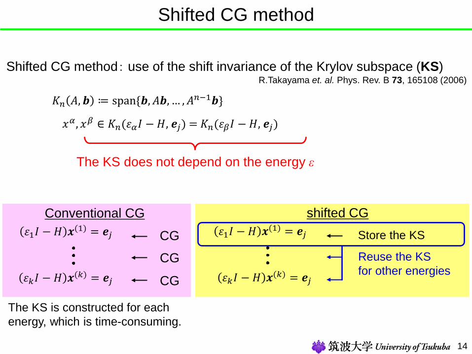
Shifted CG method
14
Shifted CG method: use of the shift invariance of the Krylov subspace (KS)
𝑥𝑥𝛼𝛼, 𝑥𝑥𝛽𝛽 ∈ 𝐾𝐾𝑛𝑛(𝜀𝜀𝛼𝛼𝑧𝑧 − 𝐻𝐻, 𝒆𝒆𝑖𝑖) = 𝐾𝐾𝑛𝑛(𝜀𝜀𝛽𝛽𝑧𝑧 − 𝐻𝐻, 𝒆𝒆𝑖𝑖)
𝐾𝐾𝑛𝑛 𝐴𝐴,𝒃𝒃 ≔ span{𝒃𝒃,𝐴𝐴𝒃𝒃, … ,𝐴𝐴𝑛𝑛−1𝒃𝒃}
The KS does not depend on the energy ε
R.Takayama et. al. Phys. Rev. B 73, 165108 (2006)
Conventional CG𝜀𝜀1𝑧𝑧 − 𝐻𝐻 𝒙𝒙(1) = 𝒆𝒆𝑖𝑖
𝜀𝜀𝑘𝑘𝑧𝑧 − 𝐻𝐻 𝒙𝒙(𝑘𝑘) = 𝒆𝒆𝑖𝑖
CGCG
CG
𝜀𝜀1𝑧𝑧 − 𝐻𝐻 𝒙𝒙(1) = 𝒆𝒆𝑖𝑖 Store the KS
Reuse the KSfor other energies
shifted CG
𝜀𝜀𝑘𝑘𝑧𝑧 − 𝐻𝐻 𝒙𝒙(𝑘𝑘) = 𝒆𝒆𝑖𝑖
The KS is constructed for each energy, which is time-consuming.

Algorithm of shifted CG method
15
𝐴𝐴𝒙𝒙 = 𝒃𝒃CG method
𝒑𝒑𝑛𝑛 = 𝒓𝒓𝑛𝑛 + 𝛽𝛽𝑛𝑛−1𝒑𝒑𝑛𝑛−1
𝛼𝛼𝑛𝑛 =𝒓𝒓𝑛𝑛𝑇𝑇𝒓𝒓𝑛𝑛𝒑𝒑𝑛𝑛𝑇𝑇𝐴𝐴𝒑𝒑𝑛𝑛
𝒙𝒙𝑛𝑛+1 = 𝒙𝒙𝑛𝑛 + 𝛼𝛼𝑛𝑛𝒑𝒑𝑛𝑛
𝒓𝒓𝑛𝑛+1 = 𝒓𝒓𝑛𝑛 − 𝛼𝛼𝑛𝑛𝐴𝐴𝒑𝒑𝑛𝑛
𝛽𝛽𝑛𝑛 =𝒓𝒓𝑛𝑛+1𝑇𝑇 𝒓𝒓𝑛𝑛+1𝒓𝒓𝑛𝑛𝑇𝑇𝒓𝒓𝑛𝑛
𝜋𝜋𝑛𝑛+1𝜎𝜎 = 𝑅𝑅𝑛𝑛+1 (−𝜎𝜎)
𝛽𝛽𝑛𝑛−1𝜎𝜎 = 𝜋𝜋𝑛𝑛−1𝜎𝜎 /𝜋𝜋𝑛𝑛𝜎𝜎 2𝛽𝛽𝑛𝑛−1
𝛼𝛼𝑛𝑛𝜎𝜎 = 𝜋𝜋𝑛𝑛𝜎𝜎/𝜋𝜋𝑛𝑛+1𝜎𝜎 𝛼𝛼𝑛𝑛
𝒑𝒑𝑛𝑛𝜎𝜎 = ⁄1 𝜋𝜋𝑛𝑛𝜎𝜎 𝒓𝒓𝑛𝑛 + 𝛽𝛽𝑛𝑛−1𝜎𝜎 𝒑𝒑𝑛𝑛−1𝜎𝜎
𝒙𝒙𝑛𝑛+1𝜎𝜎 = 𝒙𝒙𝑛𝑛𝜎𝜎 + α𝑛𝑛𝜎𝜎𝒑𝒑𝑛𝑛𝜎𝜎
𝛼𝛼,𝛽𝛽, 𝒓𝒓
(𝐴𝐴 + 𝜎𝜎𝑧𝑧)𝒙𝒙𝜎𝜎 = 𝒃𝒃
scalar-vector product
matrix-vector productvector-vector product
Computationally moderate!
Shifted CG method
But, this method is applicable only for linear equations.

Advantage of computing unperturbed Green’s functions
16
1
)(0)(
)(0)(
ˆ
1
1
0−
−−−−−
−−−−−
=
+m
m
zAEBBzAEB
BzAEBBzAE
g
†
†
†
Unperturbed Green’s function does not include electrode effect.
Shifted linear equations & fast on massively parallel computers
(𝑧𝑧𝑧𝑧 − 𝐻𝐻)𝑔𝑔 =
00
Process 0
Process 1
Process 2
Process 3
Load unbalance does not happen.

Relation between perturbed and unperturbed GFs
17
.
)(0
0)(
,11
,00
1,1,11,10,1
1,,1,0,
1,1,11,10,1
1,0,01,00,0
,1
,
,
,1
,0
Σ
Σ
=
+++++++
+
+
+
+ lmmR
lL
mmmmmm
mmmmmm
mm
mm
lm
lm
ll
l
l
Gz
I
Gz
gggggggg
gggggggg
GG
G
GG
←l th row
Dyson's equation in the standard form is
.)()()()(
,1
,0
,1
,0
1,110,1
1,000,0
−=
−ΣΣ
Σ−Σ
+++++
+
lm
l
lm
l
mRmmLm
mRmL
gg
GG
IzgzgzgIzg
gHere, is kth block line and lth block row of .lkg ,
From 0 th, l th, and m+1 th block rows, we have
By solving the above equations, we obtain the relation between perturbed Green’s function and unperturbed Green’s function .
[ ] 11,111,11,1
~)(~ −Σ−= gzIgG L [ ] 1,1
,,11,1 )()( mmRmmmRm gzgIzgg −Σ−Σ+1,1~gwith being .
Proof is in T. Ono et al., PRB 86 195406 (2012).
G g

Effect of shifted CG method
18
0 10 20 30 40 500
500
1000
1500
2000
2500
3000 Shifted CG R.Takayamaet al, PRB73, 165108 (2006)
CG
CP
U t
ime
[sec
.]
Number of sampling energy points
×6.4
×14.6
×22.1
Shifted CG becomes powerful as the number of sampling points increases!
Intel Xeon E5-2690 2.90GHz
Collaboration with Prof. Cho (Nagoya U.) and Prof. Hoshi (Tottori U.)Computational model (Na nanowire)

Power Transmission
19
10% of electronic power is lost as heat(10%=80TeraWh/year )
SiC is one of the promising candidates to replace Si!
Technological limit of Si-based power devices is approachingbecause the band gap of Si is small for power devices.
Power devicesElectronic devices for AC-DC, voltage, and frequency conversions.
Resource and energy problemloss loss
Development of low loss power conversion devices is indispensable.
loss
loss

Problems of SiC-based MOSFET
20
These problems are believed to be caused by interface defects near SiC/SiO2 interface.
Data taken from D. Okamoto et al., IEEE EDL 31 710 (2010).
Low carrier mobility Threshold voltage shift
MJ Marinella et al., APL 90 253508 (2007).
It is of importance to study the oxidation process of SiC.

Thermal oxidation of SiC
21
There may exist various C- and O-related defects at the interface, but their effect on carrier mobility is not clear.
O2
SiC
SiO2
CO desorption O2 in-diffusion
Purpose of this study is To clarify the relationship between interface atomic structures and carrier-scattering properties.

Computational method & model
22
Density Functional Theory
Optimization Transport Calculation
NEGF-Landauer method
T. Ono et al, PRB 86, 195406 (2013)S. Iwase et al, PRE 91, 063305 (2015)
Σ𝐿𝐿 Σ𝑅𝑅
𝑇𝑇(𝐸𝐸) = Tr[�Γ𝐿𝐿 �𝐺𝐺𝑟𝑟 �Γ𝑅𝑅 �𝐺𝐺𝑟𝑟† ]
𝑧𝑧(𝑉𝑉) =2𝑒𝑒ℎ�𝜇𝜇𝑅𝑅
𝜇𝜇𝐿𝐿𝑑𝑑𝐸𝐸 𝑇𝑇(𝐸𝐸)
e
O atom
Real-space finite-difference
Projector augmented wave (PAW)
Local density approximation (LDA)
T. Ono et al, PRB 82, 205115 (2010)
code is employed

Two types of surface & interface
23
4H-SiC(0001) has stacking sequence of ABCBAB…. shows two types of surface.
Cubic(K) interface
A
B
C
B
B
C
B
A A
Hexagonal(H) interface
Interface modelsAFM image
K. Arima et al, APL 90 202106 (2009)
H faceK face
H face
CBA
BA

Interface atomic structures during thermal oxidation
24
Thermal oxidation of 4H-SiC(0001) undergoes as following steps.
1. Clean 2. Oint 3. O2int 4. VCO2
Carrier scattering properties of above 4 models are examined for K and H interfaces.
O O
CO
O

I-V curve
25
K interface H interface
• C interface is more sensitive to the insertion of O atoms than H interface.• Just single inserted O atom at K interface reduces conductance!

Conduction band edge states of SiC
26
Y. Matsushita et al., PRL108 246404 (2012).
Si SiC
• Nearly free electron (NFE) like
• Accumulating at inter layer• Easily affected by stacking sequence
• sp3 anti-bonding state• Localized around Si atoms
• Stacking sequence of SiC affects the behavior of the NFE states at the interface.
• Control of the NFE states is an important issue to improve the carrier mobility of SiC-MOSFET!

Summary
27
• As the progress of parallel computers, the real-space methods for first-principles calculations are developed.
• With this stream, RSPACE has been developed.
• Electronic current in nanoscale systems is quite different from that in macroscale systems. Although it is difficult for the conventional methods toexamine this phenomena, RSPACE can investigate owing to the flexibilityof boundary conditions.
• Computation of the perturbed Green’s function is one of the bottle necks intransport calculations. We have overcome by the shifted CG method andgood scalability of the real-space method.
• Low carrier mobility at SiC/SiO2 hampers the realization of SiC-MOSFET.To improve the mobility, control of the NFE states lying the conduction bandedge is important.
Development of RSPACE code
Application(Carrier scattering property of SiC-MOS interface)