real-time adaptation to antenna impedance...
TRANSCRIPT

Real-time Adaptation to Antenna
Impedance Mismatch for CDMA
Transceivers
Dongjiang Qiao, *David Choi, Yu Zhao, **Dylan Kelly,
Tsaipi Hung, Donald Kimball, Mingyuan Li, and Peter Asbeck
University of California, San Diego*Nokia Research Center, **Peregrine Semiconductor

Outline
Introduction
Design of Tunable Matching Network
Antenna Load Impedance Measurement Using Sectioned
Transmission Line
Closed-loop Measurement Results
Conclusions
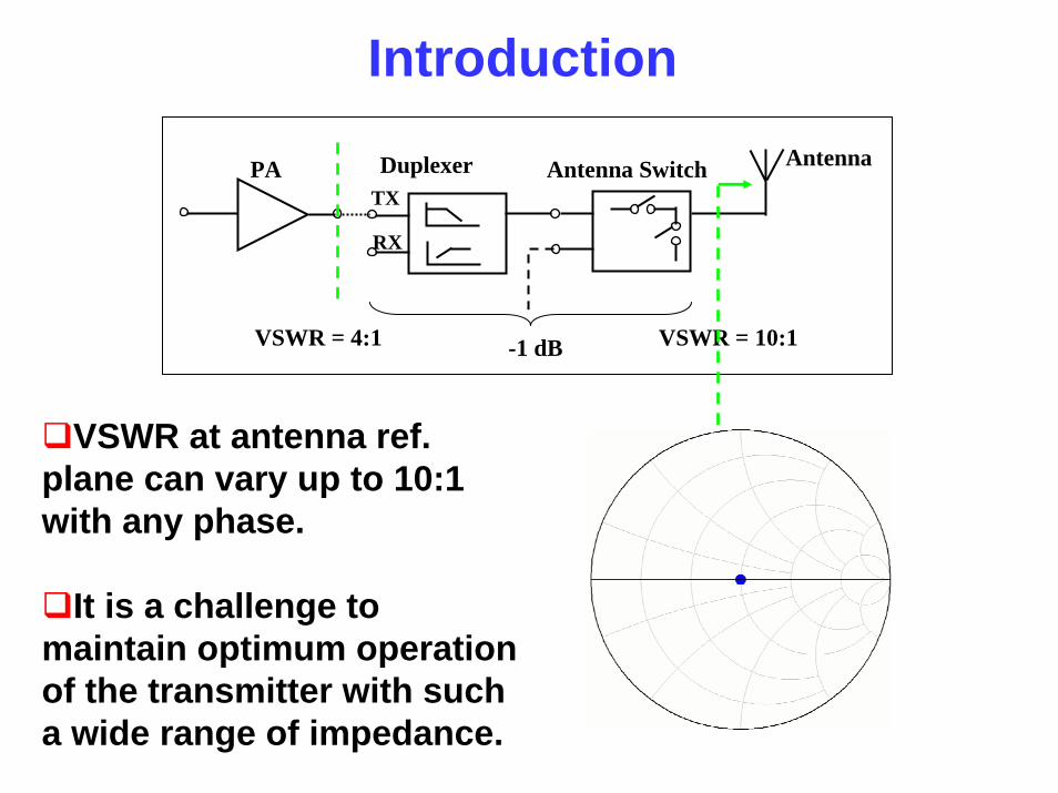
Introduction
-1 dBVSWR = 4:1 VSWR = 10:1
PA Duplexer Antenna Switch Antenna
TX
RX
VSWR at antenna ref. plane can vary up to 10:1 with any phase.
It is a challenge to maintain optimum operation of the transmitter with such a wide range of impedance.

Performance of PA with Different Load
ADS simulation results for a class AB amplifier designed for 50 ohm
Mismatch Also Impacts:Stability: Possible oscillation of power
amplifier thus damaging the amplifierDuplexer insertion loss
5 10 15 20 25 30 350
5
10
15
20
25
Gai
n (d
B)
Pout (dBm)5 10 15 20 25 30 35
0
20
40
60
80 50 ohm 12.5 ohm 200 ohm
PA
E (%
)
Pout (dBm)
5 10 15 20 25 30 35-50
-40
-30
-20
IMD
3 (d
Bc)
Pout (dBm)

Adaptive Transmitter
PA Duplexer
Antenna
Controller
TX
RXLNA
Impedance measurement
Tunable matching network

Tunable Matching Network With Silicon-on-Sapphire Switches
L1 L2
C1 C2
L1 L2
C11 C22C12 C13 C21 C23
S21 S22 S23S13S12S11
– Stack of 6×6 parallel available – W/L = 6000um/0.5um per FET– Ron and Coff scale linearly with stacking /
adding parallel devices– BVDSS (2 nA/um) = 2 V– Recommend +/- 2 to 3 V bias– Ron = 0.5 ohm (2.75 ohm-mm) @ 3 V– Coff = 1.8 pF (300 fF/mm)– Gate is ESD protected
Compared to bulk CMOS, SOS has:Reduced component-substrate
parasitic capacitanceImproved isolation between
transistors

Characteristics of Tunable Matching Network
Average VSWR Reduction by
Tunable Matching Network
0 2 4 6 81.0
1.2
1.4
1.6
1.8
2.0
VSW
R w
Cor
rect
ion
VSWR w/o Correction
Available impedance of the tuner
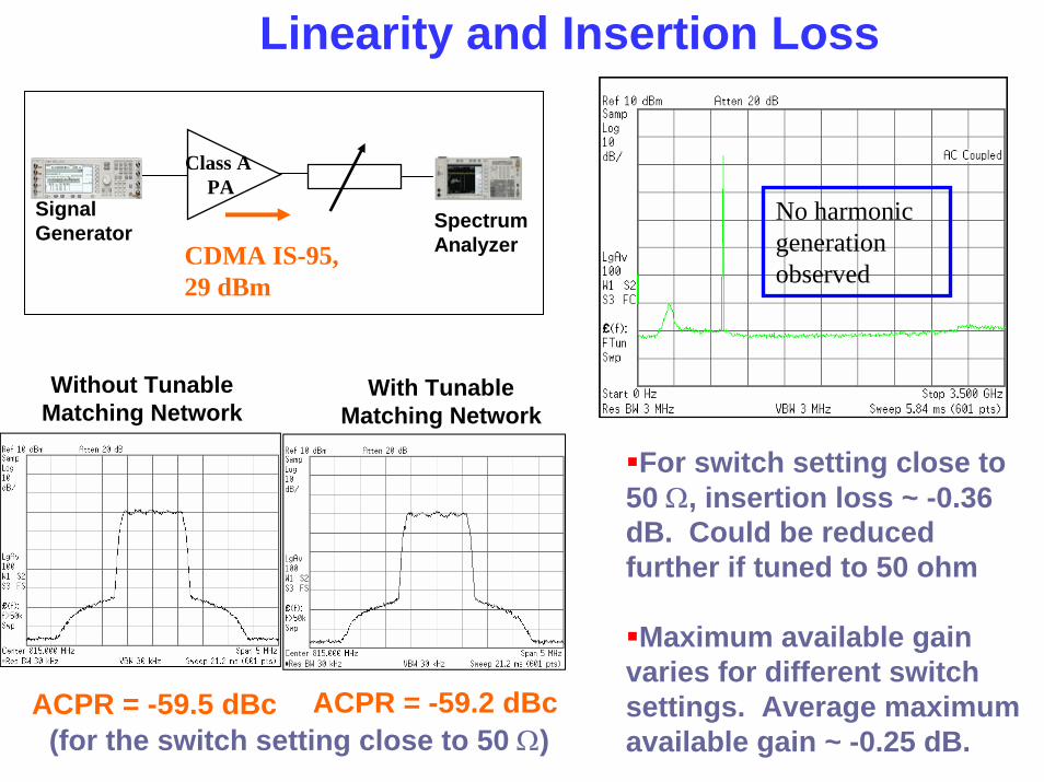
Linearity and Insertion Loss
For switch setting close to 50 Ω, insertion loss ~ -0.36 dB. Could be reduced further if tuned to 50 ohm
Maximum available gain varies for different switch settings. Average maximum available gain ~ -0.25 dB.
Without TunableMatching Network
ACPR = -59.5 dBc ACPR = -59.2 dBc
With Tunable Matching Network
No harmonic generation observed
Class A PA
CDMA IS-95, 29 dBm
Signal Generator Spectrum
Analyzer
(for the switch setting close to 50 Ω)

Measurement of Load Impedance Using Transmission Line
( ) [ ]zjzjo eeVzV ββ Γ+= −+
0.5 1.0 1.5 2.00.0 2.5
-0.5
0.0
0.5
-1.0
1.0
time, nsec
ts(V
2), V
0.5 1.0 1.5 2.00.0 2.5
-0.5
0.0
0.5
-1.0
1.0
time, nsec
ts(V
1), V
0.5 1.0 1.5 2.00.0 2.5
-0.5
0.0
0.5
-1.0
1.0
time, nsec
ts(V
out)
, V
+
-ZL
ILV(z), I(z)
Z0, β
z1z2z3
zjo eV β−+
zjo eV βΓ+
Z0 = 50 ohm, ZL = 15 ohm, 90o Transmission Line
0
0ZZZZ
L
L+−
=Γ LCw=β
22
11
2
1zjzj
zjzj
z
z
eeee
VVr ββ
ββ
Γ+Γ+
== −
−
Measurement results depend on voltage ratios, not the voltages
Independent of input power and the source impedance

Measurement Setup
Fabricated on PCB board¼ λ transmission line815 MHzSingle tone and CDMA IS-95
Measured by Network AnalyzerMeasured by Transmission Line
CDMAThree input power levels (12, 14 and 16 dBm)

Load Impedance Measured by Artificial TL
Coilcraft inductors (Q > 100)CDMA IS-95
Part of the error was caused by the fact that the lumped elements do not have the same values as calculated for the artificial transmission line
0.65 0.70 0.75 0.80 0.85 0.90 0.950.60 1.00
-0.40
-0.35
-0.30
-0.25
-0.45
-0.20
freq, GHz
dB
(S(2
,1))
m4
m4freq=dB(S(2,1))=-0.331
815.0MHz
Z0
45o 45o
LL4
R=L=6.9 nH
CC6C=1.62 pF
CC5C=1.62 pF
CC4C=3.24 pF
LL3
R=L=6.9 nH
Measured by Network AnalyzerMeasured by Transmission Line

PA with Closed-loop Control
CDMA PA
Controller
Impedance measurement
Tunable matching network
Mechanical Tuner
Feedback Path Signal Generator
SpectrumAnalyzer
Control logic: voltages ratios are tuned close to 1 by changingswitch settings (load impedance close to 50 Ω)
GPIB interface controlled by LabView
Skyworks CDMA Handset PA CX77105 (GaAs HBT)
IS-95, 824MHz, Fixed 0 dBm Pin (~ 28 dBm Pout for 50 Ω)
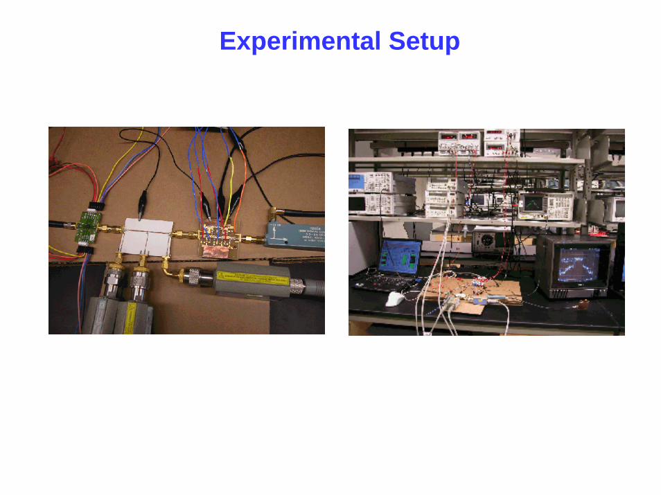
Experimental Setup

Improvement of Power Amplifier Performance
Average results for VSWRs with different phase
1 2 3 4 5 6 7 8
12
16
20
24
28
0
10
20
30
40
50
Pout
w/o correction w/ correctionPo
ut (d
Bm
)
VSWR
PAE
PA
E (%
)
w/o correction w/ correction
1 2 3 4 5 6 7 8
-50
-40
-30
-20
-10
0
AC
PR fo
r wor
st c
ase
VSWR
w/o correction w/ correction
For 8:1 VSWR
–Pout improved by 2.8 dB
–PAE improved by × 2 times
–Worst ACPR reduced 4 dB

Impact of Load Impedance Mismatch on Duplexer(EPCOS B4224 SAW Duplexer Filter: Measured Data)
ZL = 50 Ω, Receiving Band
0.75 0.80 0.85 0.90 0.950.70 1.00
-60
-40
-20
-80
0
freq, GHz
dB
(S(1
,2))
m2m3
m2freq=dB(S(1,2))=-2.973
894.0MHz
m3freq=dB(S(1,2))=-2.756
869.0MHzReceivingPort I Mechanical Tuner
TransmissionPort IIIterminated with 50 Ω
AntennaPort II
ZL
Mechanical TunerTunable Matching Network
VSWR Correction
0.8 0.90.7 1.0
-40
-20
-60
0
freq, GHz
dB(S
(1,2
))
m2
dB(u
nc..
S(1
,2))
m3m2freq=dB(S(1,2))=-4.896
869.0MHz
m3freq=dB(unc..S(1,2))=-8.453
869.0MHz
Average results for 8:1 VSWR
–S12 ↑ 2.5 dB

Summary
Antenna load impedance mismatch has been effectively reduced using a tunable matching network implemented using SOS switches.
A method has been developed to measure the antenna load impedance based on measurement of the voltages along a transmission line.
With closed loop correction of the impedance mismatch, the output power, PAE and linearity of a PA have been improved; the in-band insertion of duplexer has been reduced.