real-time diagnostics of growth of silicon-germanium alloys on hydrogen-terminated and oxidized...
TRANSCRIPT
Thin Solid Films 343-333 (1999) 477-132
Real-time diagnostics of growth of silicon-germanium alloys on hydrogen-terminated and oxidized silicon (111) surfaces by
spectroscopic ellipsometry
Abstract
Chemical vapor deposition of amorphous hydrogenated silicon-germanium alloys (a-SiGe:H) was induced by photolysis of disilane and digermane mixtures with an ArF laser at 193 nm. The gro\& behavior on hydrogen-terminated and oxide-covered SiiI 1 I) surfaces was studied in real time in the monoIayer region by spectroscopic ellipsomerry (1.24.7 eVj. One-, tlvo- and three-layer models were employed ro simuiate the ellipsometric data. For the fiat hydrogen-terminated siricon surface the slow formation of a well-defined monolayer is extracted from the analysis. On the native oxide-covered surface fast initial 3D growth ~3s observed with coalescence at a larger film thichess. A rhree-layer mode1 was needed to describe the _erowth of ultrathin films after coalescence, where a third layer, with a thickness in the nanometer range, takes into account the Lower quality of the ultrathin fiLm layer near the interface. 0 1999 EIsevier Science S.A. All rights reserved.
Keywords: Chemical vapnr deposifion; Etiipsometry; Optical properties; Semiconductors
1. Introduction
Amorphous hydrogenated silicon-germanium alloys (a- SiGe:Hj have attracted much interest for wious optoelec- tronic applications due to the possibility of adjusting their optical bandgap. Their practical use, however, is so far limited by poor photoelectric properties. The degradation of the fXm quality with ailoying is explained by the exis- tence of inhomogeneities in both composition and SCIW- we. Especially the quality of the interface becomes mofe and more important for applications using ultra-thin films. To come to a better understanding of these problems it is necessary to investigate the nature and formation of defects and the quality of the interface layer on a molecular level.
Plasma deposition is currently the technique used most commonly to produce this material [l-3]. In these studies the basic structural, optical, and electrical properties of the alloys deposited by plasma-enhanced chemical vapor deposition (CVD) were characterized. Photochemical yapor deposition was also investigated in detail using, for example, an ArF Iaser 1193 nm) to photolyze GeH$$~ mixtures [4] or Ge2HJSi2Ho mixtures [5]. The growth of
* Corresponding author. Tel,: Jr 49-6221-545205; f&x: f 49-6221- 544255.
E-maii nddress: [email protected] (P. Hess)
solid films by CVD processes is connected with a large number of gas-phase and surface reactions, which are presently not understood vety well. Considerable progress has been made recently and can be expected in the near future in elucidating these very complicated scenarios by linear and nonlinear optical probing techniques as discussed in a recent review [6].
Optical probing has the advantage that it can be applied in situ and in real time. It does not need vacuum conditions, is usually nondestructke, and provides specific information on the growing material such as the chemical bonding config- uration using FTR spectroscopy in the infrared [7] or opti- cal properties such as the refractive index or dielectric constants in the yisible and ultraviolet using spectroscopic ellipsometry [S]. Nilthough optical diagnostics is macro- scopic in nature. its resuits are Linked to the microscopic properties of the solid surface. In combination with suitable models, optical techniques provide a detailed molecular picmre of the surface and growth processes.
Here we report on the real-time diagnostics of a-SiGe:H growth by spectroscopic ellipsometry in the very first stage of surface reactions. The nucleation process is studied for a hydrogen-terminated silicon (I 11) substrate and one with its natural oxide layer. Information on the structure of the first layers is extracted from the ellipsometric measurements by fitting the data with a sui&bIe model. This reveals, for
OOQI-6090!99/$ - see front matter 0 1999 Elsevier Science S.A. .klI rights reserved PII: SOO10-6090(9SIOl685-X
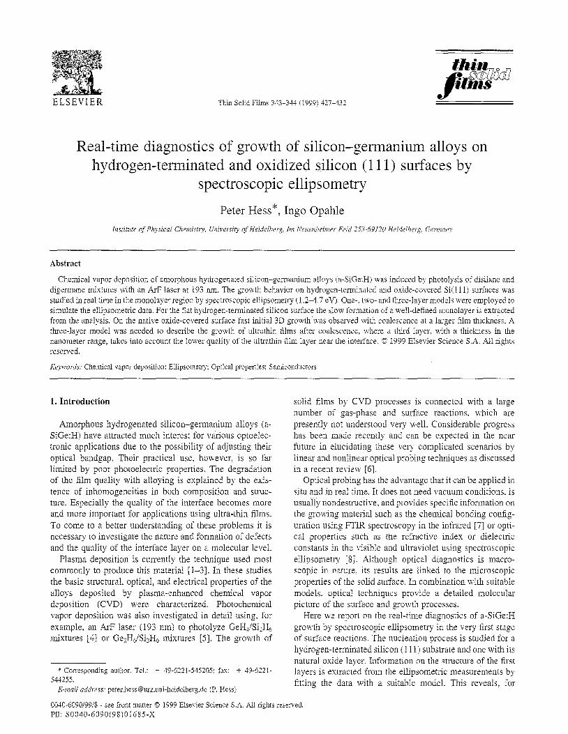
FIN. I. Experimental set-up for laser CVD and spectroscopic ellipsxnerry.
example. the strong dependence of the growth process on the nature of the substrate surface.
2. Experimental
Fig. 1 shows a scheme of the experimental set-up with the ArF laser for initiating the CVD process, the UHV chamber with the substrate. and the spectroscopic ellipsometer for real-time diagnostics of the deposition process.
The ArF laser induced the CVD process in parallel laser beam-substrate configuration. The laser power was varied between 0.5 and 3 W. At 0.5 W the hydrogen content was about 6%. the SiHJSiH ratio 0.56 and the GeH/SiH ratio 0.1-l for a substrate temperature of 290°C. With increasing laser power and decreasing substrate temperature, the hydrogen content and amount of SiHl groups increased and degraded the electronic properties of the material due to strong distortions of the solid network. All results presented here were obtained at 290°C.
The total pressure of the deposition gases and the helium buffer gas was typically 1.5 mbar. The partial pressure of the
1200 7
I Ge -Ge
800
2 600 x x kj 400 =
200
Ge -Si
0 I 1
200 300 400 500 600
Raman shift (cm ‘I)
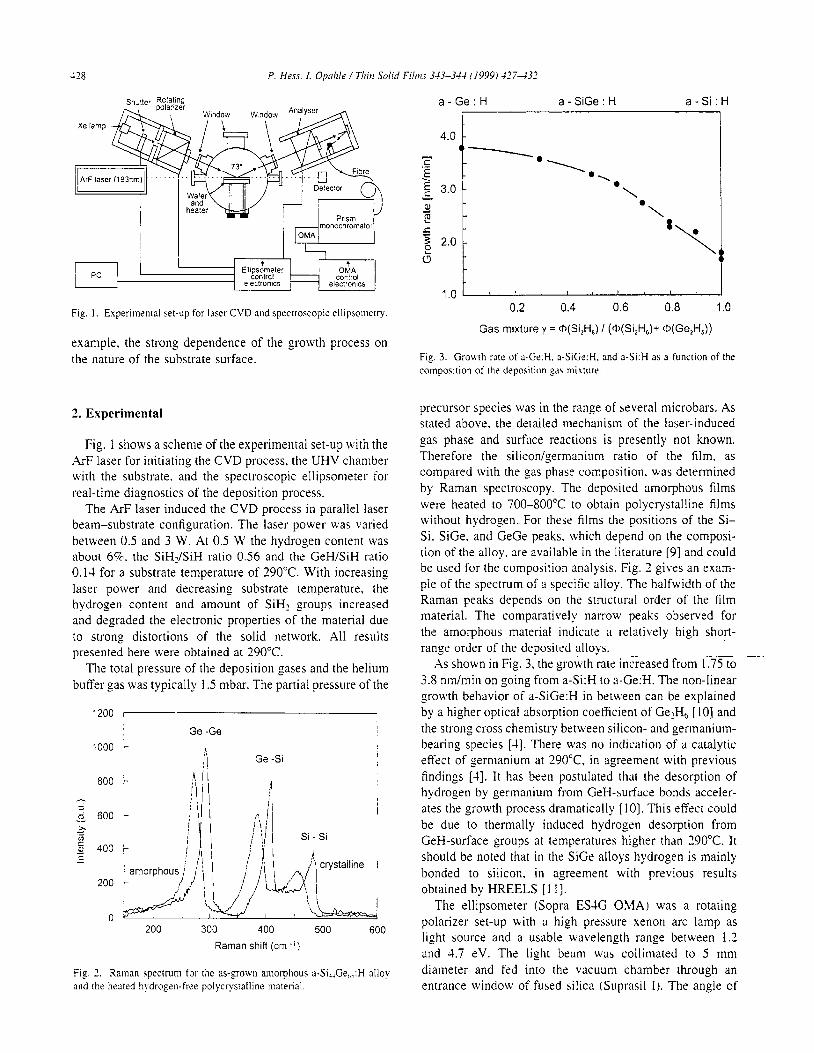
Fio 2 3. -. Raman \pecirum for rhe as-grown amorphous a-Si,,Ge,,.,:H alloy
and the heated hydrogen-free polycrysralline material.
a-Ge:H
4.0 t
a - SiGe : H a - Si : H
1
\
1.0 I , 0.2 0.4 0.6 0.8 1.0
Gas mixture y = @(S&H,) / ((I)(Si,H,)+ (P(Ge,H,))
Fi_p. 3. Grouth rafe of a-Gr:H. a-SiCkH. and a-Si:H as a funcrion of the
composirion of the deposition ga\ mixture.
precursor species was in the range of several microbars. As stated above. the detailed mechanism of the laser-induced gas phase and surface reactions is presently not known. Therefore the silicon/germanium ratio of the film. as compared with the gas phase composition. was determined by Raman spectroscopy. The deposited amorphous films were heated to 700-800°C lo obtain polycrystalline films without hydrogen- For these films the positions of the Si- Si. SiGe. and GeGe peaks. which depend on the composi- tion of the alloy. are available in the literature [9] and could be used for the composition analysis. Fig. 2 gives an exam- ple of the spectrum of a specific alloy. The halfwidth of the Raman peaks depends on the structural order of the film material. The comparatively narrow peaks observed for the amorphous material indicate a relatively high short- range order of the deposited alloys.
As shown in Fig. 3, the growth rate in&eased from I .75 to 3.8 nm/min on going from a-Si:H to a-Ge:H. The non-linear growth behavior of a-SiGe:H in between can be explained by a higher optical absorption coefficient of Ge:H, [lo] and the strong cross chemistry between silicon- and germanium- bearing species [J]. There was no indication of a catalytic effect of germanium at 290°C. in agreement with previous findings [-$I. It has been postulated that the desorption of hydrogen by germanium from GeH-surface bonds acceler- ates the growth process dramatically [IO]. This effect could be due to thermally induced hydrogen desorption from GeH-surface groups at temperatures higher than 190°C. It should be noted that in the SiGe alloys hydrogen is mainly bonded to silicon. in agreement with previous results obtained by HREELS [I 11.
The ellipsometer (Sopra ESJG O.MA) was a rotating polarizer set-up with a high pressure xenon arc lamp as light source and a usable wavelength range between I.2 and 1.7 eV. The light beam was collimated to 5 mm diameter and fed into the vacuum chamber through an entrance window of fused silica (Suprasil I). The angle of
P. Hess. 1. Opahle / Thin Solid Films 343-344 (19991 427432 ‘$29
6
0 3.0 3.5 4.0 4.5
Pf,G!On energy [evj
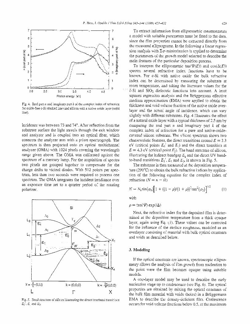
Fig. ii. Real part TZ and imaginary part k of tk complex index of refraction for oxide-free c-Si (dashed line) and silicon wit11 a native oxide layer (solid line).
incidence was between 73 and 74”. After reflection from the substrate surface the light travels through Ihe e,xit window and analyzer and is coupled into an optical fiber. which connects the analyzer arm with a prism spectrograph. The spectrum is then projected onto an optical multichannel analyzer (OMA) with 1024 pixels covering the wavelength range given above. The OMA was calibrated against the spectrum of a mercury lamp. For the acquisition of spectra two pixels are grouped together LO compensate for the charge drifts to vicinal diodes. With 512 points per spec- trum, less than two seconds were required to process one spectrum. The OLMA integrates the incident it-radiance over an exposure time set to a quarter period of the rotating polarizer.
k= (O:O,O)
r
Fig. 5. Band structure of siiicon illustrating the direct interband transitions Eo’. El and E!.
To exwact information from ellipsometric measurements a model with suitable parameters must be fitted to the dara, since the film properties cannot be extracted directly from the measured eilipsograms. In the following a linear regres- sion analysis with Ca-minimization is appIied to determine the parameters of the growth model selected to describe the main features of the particular deposition process.
To interpret the ellipsometric tan(XP(Ei) and cos(il{E)) spectra severai refractive index functions have to be known. For c-Si with native oxide the bulk refractive index can be determined by measuring the substrate at room temperature, and taking the literature values for the T-Si and SiO? dielectric functions into account. A least squares regression analysis and rhe Brtiggemann effective medium approximation (E&M) were applied to obtain the thickness and void volume fraction of the native oxide over- layer and the actual angle of incidence, which can vary slightly with different substrates. Fig. 4 iilustrates the effect of a natural oxide layer with a typical thickness of 2.5 nm by comparing the real part 71 and imaginary part X- of the complex index of refraction for a pure and native-otide- covered silicon substrate. The silicon spectrum shows two characteristic features, the direct transitions around E = 3.3 eV (criticai poinls ED’ and El) and the direct transition at E = 4.3 eV (critical point Ez), The band structure of silicon, illustrating the indirect bandgap Eg and the direct UV band- to-band transitions Eo', E, and El, is shown in Fig. 5.
The substrate is then measured at the deposition tempera- ture (29O”Cj to obtain the bulk refractive indices by applica- tion of the following equation for the complex index of refraction (N = rr - iX-)
N = :vOsin(pO)[ I + ((1 - p)/(l + ~))3tan’(~0)]1’z (1)
with
p = fan{ ?E, expiiilj
Next. the refractive indes for the deposited film is deter- mined at the deposition temperature from a thick opaque layer, again using Eq. (1). These values can be corrected for the influence of the surface roughness, modeled as an overlayer consisting of material with bulk optical constants and voids as described below.
3. Modeling
If the optical constants are tiown, spectroscopic ellipso- metry allows the analysis of film growth from nucleation to the point were the film becomes opaque using suitable models.
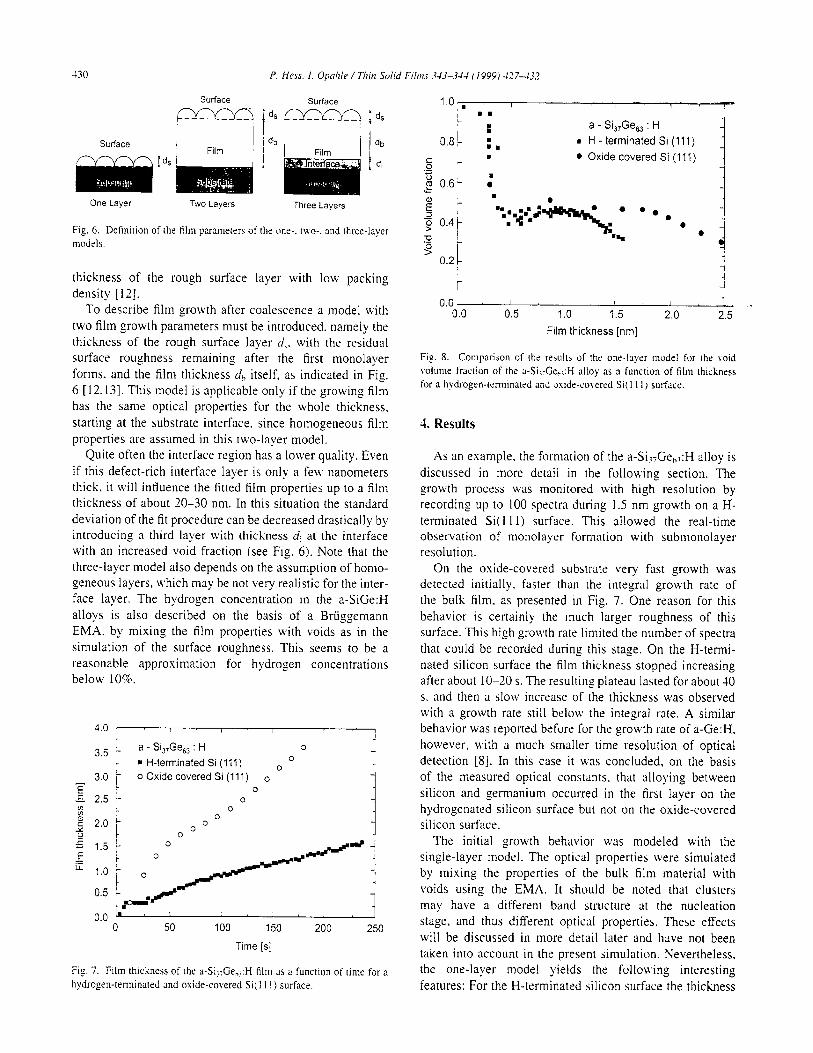
A one-layer model may be used to describe the earIJ nucleation stage up to coalescence (see Fig. 6). The optical properties are obtained by mixing the optical constants of the bulk film material with voids (holes) in a Brtiggemann EMA to describe the density-deficient film. Coalescence occurs for void volume fractions below 05, at Ihe maximum
Surface / ,
1 d,
One Layer T:vo Layers Three Layea
Fig. 6. Definition of the film pzrameterl: of the one-. MO-, nnd three-layer models.
thickness of the rough surface layer with low packing density [ 121.
To describe film growth after coalescence a model with two film growth parameters must be introduced. namely the thickness of the rough surface layer d,. with the residual surface roughness remaining after the first monolayer forms. and the film thickness ti, itself, as indicated in Fig. 6 [ 12.131. This model is applicable only if the growing film has the same optical properties for the whole thickness. starting at the substrate interface. since homogeneous film properties are assumed in this two-layer model.
Quite often the interface region has a lower quality. Even if this defect-rich interface layer is only a few nanometers thick. it will influence the fitted film properties up to a film thickness of about ‘O-30 nm. In this situation the standard deviation of the fit procedure can be decreased drastically by introducing a third layer with thickness cl: at the interface with an increased void fraction (see Fig. 6). Note that the three-layer model also depends on the assumption of homo- geneous layers, Lvhich may be not very realistic for the inter- face layer. The hydrogen concentration in the a-SiGe:H alloys is also described on the basis of a Briiggemann EMA. by mixing the film properties with voids as in the simulation of the surface roughness. This seems to be a reasonable approximation for hydrogen concentrations below 10%.
4.0 I I
- 3.5 L a Si3,Gec3 : H 3
_ n H-terminated Si (111) 0
1
3 3.0 o Oxide covered Si (111) o
F c 2.5 L
0 0
0.0 '= 0 50 100 150 200 250
Time [sj
Fif. 7. Film thickness of rhr a-Si,:Ge,,,:H film 3s i! function of rime for a hydrogen-wminated und oxide-covered SIC 11 1) surface.
1.0,. I 1 ? . .
0.8 L e a - Si,,Ge, : H
:. n H - terminated Si (111)
s - . l Oxide covered Si (111)
‘S
0.0 0.0 I 0.5 I I I ! ” 1.0 1.5 2.0 2.5
Film thickness [nm]
Fig. 8. Compnrijon of the rwlb of the one-lnyer model for the boid volume fraction of the a-Si;rCe,.l:H alloy as 3. function of film thickness for a hydrogen-wrminared and wide-covered Si( I I I) surfxc.
4. Results
As an example. the formation of the a-Si;iGe,l:H alloy is discussed in more detail in the following section. The growth process was monitored Lvith high resolution by recording up to 100 spectra during 1.5 nm growth on a H- terminated Si( 1 II) surface. This allowed the real-time observation of monolayer formation with submonolayer resolution.
On the oxide-covered substrate very fast growth was detected initially, faster than the integral growth rate of the bulk film. as presented in Fig. 7. One reason for this behavior is certainly the much larger roughness of this surface. This high growth rate limited the number of spectra that could be recorded during this stage. On the H-termi- nated silicon surface the film thickness stopped increasing after about lo-20 s. The resulting plateau lasted for about 10 s. and then a slow increase of the thickness was observed with a growth rate still below the integral rate. A similar behavior was reported before for the growth rate of a-Ge:H, however. with a much smaller time resolution of optical detection [S]. In this case it was concluded, on the basis of the measured optical constants. that alloying between silicon and germanium occurred in the first layer on the hydrogenated silicon surface but not on the oxide-covered silicon surface.
The initial growth behavior ws modeled with the single-layer model. The optical properties were simulated by mixing the properties of the bulk film material with voids using the EMA. It should be noted that clusters may have a different band structure at the nucleation stage, and thus diRerent optical properties. These effects will be discussed in more detail later and have not been taken into account in the present simulation. Nevertheless, the one-layer model yields the following interesting features: For the H-terminated silicon surface the thickness
P. Hess, I. Opahle / Thin Sdid Fiirns 343-344 11959) 427432 ii31
0.0 $ ! / , t , < 0.0 1, / , 1 ( , , j 0 20 40 60 eo 0 20 40 60 80
Flln thickness [m] F:im thickness [nn]
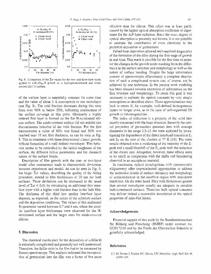
Fig. 9. Comparison of the Z~T values for the twc- and tier-layer model applied to a-Si3,G~3:H growth on a hydrogen-terminated and oxide- covered Sii 1 I 1) surface.
of the surface layer is essentially constant for some time s and the value of about 3 A corresponds to one monolayer (see Fig. 8). The void fraction decreases during this time from over 90% to below 50%, indicating coalescence of the surface coverage at this point. Obviously a highly ordered first layer is formed on the flat H-terminated sili- con surface. The oxide-covered surface did not exhibit this discontinuous behavior of the void fraction. For the first measurement a value of 60% was found and 50% was reached near 10 run film thickness, as can be seen in Fig. 8. This is consistent with three-dimensional cIuster growth, without formation of a well defined monolayer. This beha- vior seems to be controlled by the initial roughness of the surface, the different lattice parameters. and the chemical nature of the surface bonds.
Description of film growth with the one- or two-layer model after coalescence leads to characteristic deviations between experiment and model. As can be seen in Fig. 9, the larger 2g values, describing the quality of the fitting procedure. extend to film thicknesses of 20 nm for both surfaces. These deviations can be decreased to the usual level of zrr < 0.01 by introducing an additional thin inter- face layer with a higher void fraction than in the bulk film. The thickness of this third low quality interface layer depends, as expected, on the nature of the substrate surface and the deposition conditions. The vaiues of [his additional fit parameter varied between 0.7 and 4 nm, where the smal- ler interface layer thicknesses were observed for the H- terminated surface and the larger ones for oxide-covered silicon.
5. Discussion
The chemicai mechanism for the deposition of a-SiGe:H is extremely complicated and presently not well understood. Therefore, the SiiGe ratio in the film had to be measured by Raman spectroscopy. This analysis indicated thar incorpora- tion of germanium into the film was a factor of five more
effective than for silicon. This effect was at least partly caused by the higher optical absorption coefficient of diger- mane for the ArF-laser radiation. Since the exact degree of optical absorption is presently not known, it is not possible to estimate the contribution of cross chemistry to the preferred deposition of germanium.
Pulsed laser deposition allowed weil-resolved diagnostics of the formation of the alloy during the first stage of growth in real time. This made it possible for the first time to moni- tor the changes in the growth mode resulting from the differ- ences in Ihe surface structure and morphology as well as the nature of surface bonding. Despite the large information content of spectroscopic ellipsomerry a complete descrip- tion of such a complicated system can, of course, not be achieved by one technique. In the present work modeling has been oriented towards extraction of information on the film structure and morphology. To reach this goal it was necessary co estimate the optical constants by very simpIe assumptions as described above. These approximations may lead to errors if, for example, well-defined homogeneous Iayers no longer exist, as in the case of self-organized 3D growth or inhomogeneities.
The index of refraction is a property of the soIid inti- mately connected with the band structure. Recently the opti- cal properties of germanium quantum dots with alterage diameters in the range 2.5-13 nm were analyzed by inves- tigating the dependence of the direct interband transitions E, and E? on the size of the clusters at 77 K [14]. The main resuIts obtained were a weakening of the intensity of the ET peak and a small blueshift of the E? peak with the reduction of the cluster size. Altogether, however, these effects seem to be small in comparison with the shifts and broadening observed in an amorphous material.
In conclusion, opticai investigations with spectroscopic ellipsometry offer unprecedented opportunities to address the moIecular details of surface chemistry and morphology of semiconductors in the interface region with monolayer resolution. On the other hand, films with thicknesses greater than several monolayers usually are adequate to simulate bulk-terminated surfaces. Therefore bulk optical constants may deliver indeed a reasonable description of the optical properties of uitra-thin layers.
Acknowledgements
Financial support of this work by the Bundesministerium fir Bildung und Forschung (BMBF) under contract no. 0329172A9 and by rhe Fonds der Chemischen lndustrie is gratefully acknowiedged.
References
[I] 31. Zeman, I. Fe&a, M.J. Gecrts, J.W. Metselaar. Xppi. Surf. Sci. 16 (19901215.
132 P. Hess, I. 0,mlde / Tlti11 Solid Films 343-344 f 1999) 4_77,/?_7
:2] V.I. Kuznersov. M. Zeman. L.L..I\. Vosreen. B.S. Guar. J.W. Merse- hr. J. Appl. Phys. SO (1996) 6196.
[3] Y.-P. Chou. S.-C. Lee. J. Appl. Phys. 83 (1998) 11 I I. [-I] H.H. Burke. I.P. Hennan. V. Tavitirn. J.G. Ed-n. Appl. Phys. Lru. 55
l19S9) 153. [5] C. Li. S. John. S. Banerjee. J. Elecrron. Mater. 3-l I 1996) 875. [6] P. Hess, m: M.D. Allendorf. C. Bernard (Eds.). Chemical Vapor
Deposirion. Procredmgs97-25. The Electrochemical Society. Pennington. NJ. 1997, pp. 616.
[7] I. Knobloch. P. Hess, Appl. Phys. Lett. 69 (1996) 4011. 181 M. Barth. P. Hess. Appl. Phys. Len. 69 ( 1996, 1710. [9] M.A. Renucci. J.B. Rznucci. M. Cardona. in: M. Balkanski (Ed.,.
Proc. Conf. on Light Scatrcring in Solids. Rammarion. Paris, 1971, pp. 31-6.
[IO] B. Meyerson. K. L;ram. F. Lcgoucs. Appl. Phys. Lett. 53 (1968) 2.555. [Ill H. Sasaki. M. Drguchi. K. Sate. $1. Aiga. J. Non-Crysl. Solids I I4
I 19S9) 671. [I?] H.V. ?4guyen, Y. Lu, S. Kim, hl. WAgi. R.W. Collins, Phys. Rev.
Lett. 74 (1995) 3880. [ I31 Y.M. Li. I. An. H.V. Nguyen, C.R. Wrunski. R.W. CoIlin>, Phys. Rev.
Lcrt. 68 (1992) 1814. [l-l] P. Toanini, L.C. Andreani. M. G&o. A. Srcllu. P. Cheyssac. R.
Kof&n. A. Migliori, Phy,. Rev. B 53 (1996) 6992.