realization of state machine - sathyabama
TRANSCRIPT

SECX1023 Programming in HDL UNIT -5 Programming Using Verilog
PREPARED BY : T.Vino
Page 1 of 31
REALIZATION OF STATE MACHINE
A sequential circuit is also known as an Algorithmic State Machine(ASM) or simply a State
Machine. These names are often used when the sequential circuit issued to control a digital
system that carries out a step-by-step procedure or algorithm. The stategraphs are used to define
state machines for controlling digital circuits like adders, multipliers,and dividers. As an
alternative to using state graphs, a special type of flowchart, called a StateMachine flowchart or
SM Chart, is also widely used to describe the behavior of a state
machine.Flowcharts are useful in software design, similarly SM Charts are useful in thehardware
design of digital systems. This is also special type of a flow chart state machineflowchart, or SM
chart for short. SM charts are also called ASM (algorithmic state machine)charts. These SM
Charts have many advantages. It is often easier to understand the operation of adigital system
by inspection of the SM chart instead of the equivalent state graph. A given SMchart can be
converted into several equivalent forms, and each form leads directly to a hardwarerealization.
SM Charts
A State Machine chart which is similar to a flow-chart is used to describe the behavior of a
digital system or state machine.State Machine charts are also known as AlgorithmicState
Machine(ASM) Chart. The ASM chart has many advantages over state graphs.It is also easy to
understand the operation of a digital system by the inspection of the SM Chartrather than the
state graph.The basic difference between an ordinary flow chart and SM chart is that ,certain
specific rulesmust be followed to constructing the SM chart ,but no such specific rules are to
be followed inthe case of flow-chart.
A State Machine Chart can be constructed from the State Graph of a Digital system.There are
three important components in an SM Chart. They are (i)State Box (ii) Decision Boxand (iii)
Conditional output Box
State Box
The state box contains a state name followed by a slash(/) and an optional outputlist. After the
state assignment ,a state code must be placed outside the box at the top.
Decision Box
A decision box is represented by the diamond shape symbol with true and False branches.
The condition placed in the box is a Boolean expression that is evaluated to determinewhich
branch is true.

SECX1023 Programming in HDL UNIT -5 Programming Using Verilog
PREPARED BY : T.Vino
Page 2 of 31
Conditional output Box
The conditional output box , which has curved ends contains a conditional output list. The
conditional outputs depend on both the state of the system and inputs.
Fig 5.1 SM Chart Component
Specific Rules for constructing SM Chart
Certain rules must be followed while constructing an SM block. For every valid combination
ofinput variables ,there must be exactly one exit path defined .This is necessary because
,eachallowable input combination must lead to a single next state.The second rule is no internal
feedback within an SM block is allowed. This is shown in the diagram below.
Fig 5.1 SM Block

SECX1023 Programming in HDL UNIT -5 Programming Using Verilog
PREPARED BY : T.Vino
Page 3 of 31
Conversion of State graph into Equivalent SM Chart:
Let us consider a state graph with three states S0, S1 and S2 as shown below. Here Za,Zb
andZc are the Moore outputs. And Z1 ,Z2 are the Mealy outputs which change after a
state changeor input change.
Fig 5.2 State Graph
The Moore outputs change only after a state change. The equivalent state chart is shown below
Fig 5.3 Equivalent State Chart

SECX1023 Programming in HDL UNIT -5 Programming Using Verilog
PREPARED BY : T.Vino
Page 4 of 31
Realization of SM Charts :
The realization of SM charts is done using similar methods used to realize state graphs.
Therealization consists of a combinational sub network ,together with flip-flops for storing the
statesof the network. Sometimes it is possible to identify equivalent states in an SM chart
andeliminate redundant states. However, in an SM chart all inputs are not tested in
every state, makes the reduction procedure more difficult. Even if the number of states in a
SMchart can be reduced, it is not always desirable to do so because combining states may make
theSM chart more difficult to interpret.
Before deriving next-state and output equations from an SM chart, a state assignment must
bemade. The best way of making the assignment depends on how the SM chart is realized. If
gatesand flip-flops (or the equivalent PLD realization) are used, the guideline method
of stateassignment is more useful.
As an example let us consider the realization of a binary counter using one PLA and two D-Flip-
flops.The SM chart of the Multiplier is shown below.
Next, the multiplier whose SM chart is shown above is implemented using a PLA and two Dflip-
flops connected, as shown in figure below. The PLA has five inputs and six outputs.
Here binary assignment is made for states.(S0 = 00, S1 = 01,etc.). Each row in the PLA tablecorr
esponds to one of the link paths in the SM chart. Because S0 has two exit paths, the table hastwo
rows for present state S0. Because only Stis tested in S0, Mand K are don’t-cares asindicated by
dashes.

SECX1023 Programming in HDL UNIT -5 Programming Using Verilog
PREPARED BY : T.Vino
Page 5 of 31
Fig 5.4 SM chart implementation using PLA and Flip-Flop
Xilinx 3000 series FPGAs
XC3000-Series Field Programmable Gate Arrays (FPGAs) provide a group of high-performance, high-
density, digital integrated circuits. Their regular, extendable, flexible, user-programmable array
architecture is composed of a configuration program store plus three types of configurable elements: a
perimeter of I/O Blocks (IOBs), a core array of Configurable Logic Bocks (CLBs) and resources for
interconnection. The general structure of an FPGA is shown in Figure 5.5. The development system
provides schematic capture and auto place-and-route for design entry. Logic and timing simulation, and
in-circuit emulation are available as design verification alternatives. The design editor is used for
interactive design optimization, and to compile the data pattern that represents the configuration program.
The FPGA user logic functions and interconnections are determined by the configuration program data
stored in internal static memory cells. The program can be loaded in any of several modes to
accommodate various system requirements. The program data resides externally in an EEPROM,
EPROM or ROM on the application circuit board, or on a floppy disk or hard disk. On-chip initialization
logic provides for optional automatic loading of program data at power-up. The companion XC17XX
Serial Configuration PROMs provide a very simple serial configuration program storage in a one-time
programmable package. The XC3000 Field Programmable Gate Array families provide a variety of logic
capacities, package styles, temperature ranges and speed grades.

SECX1023 Programming in HDL UNIT -5 Programming Using Verilog
PREPARED BY : T.Vino
Page 6 of 31
Fig 5.5 Field Programmable Gate Array Structure.
XC3000 Series Overview
There are now four distinct family groupings within the XC3000 Series of FPGA devices:
• XC3000A Family
• XC3000L Family
• XC3100A Family
• XC3100L Family
All four families share a common architecture, development software, design and programming
methodology, and also common package pin-outs. An extensive Product Description covers these
common aspects. Detailed parametric information for the XC3000A, XC3000L, XC3100A, and
XC3100L product families is then provided. (The XC3000 and XC3100 families are not recommended
for new designs.)
Here is a simple overview of those XC3000 products currently emphasized:

SECX1023 Programming in HDL UNIT -5 Programming Using Verilog
PREPARED BY : T.Vino
Page 7 of 31
• XC3000A Family — The XC3000A is an enhanced version of the basic XC3000 family, featuring
additional interconnect resources and other user-friendly enhancements.
• XC3000L Family — The XC3000L is identical in architecture and features to the XC3000A family, but
operates at a nominal supply voltage of 3.3 V. The XC3000L is the right solution for battery-operated and
low-power applications.
• XC3100A Family — The XC3100A is a performance-optimized relative of the XC3000A family. While
both families are bit stream and footprint compatible, the XC3100A family extends toggle rates to 370
MHz and in-system performance to over 80 MHz. The XC3100A family also offers one additional array
size, the XC3195A.
• XC3100L Family — The XC3100L is identical in architectures and features to the XC3100A family,
but operates at a nominal supply voltage of 3.3V.
Fig 5.6 illustrates the relationships between the families. Compared to the original XC3000 family,
XC3000A offers additional functionality and increased speed. The XC3000L family offers the same
additional functionality, but reduced speed due to its lower supply voltage of 3.3 V. The XC3100A family
offers substantially higher speed and higher density with the XC3195A.
Fig 5.6 XC3000 FPGA Families
SECX1023 Programming in HDL UNIT -5 Programming Using Verilog
PREPARED BY : T.Vino
Page 8 of 31
Detailed Functional Description
The perimeter of configurable Input/Output Blocks (IOBs) provides a programmable interface between
the internal logic array and the device package pins. The array of Configurable Logic Blocks (CLBs)
performs user-specified logic functions. The interconnect resources are programmed to form networks,
carrying logic signals among blocks, analogous to printed circuit board traces connecting MSI/SSI
packages.
The block logic functions are implemented by programmed look-up tables. Functional options are
implemented by program-controlled multiplexers. Interconnecting networks between blocks are
implemented with metal segments joined by program-controlled pass transistors.
These FPGA functions are established by a configuration program which is loaded into an internal,
distributed array of configuration memory cells. The configuration program is loaded into the device at
power-up and may be reloaded on command. The FPGA includes logic and control signals to implement
automatic or passive configuration. Program data may be either bit serial or byte parallel. The
development system generates the configuration program bit stream used to configure the device. The
memory loading process is independent of the user logic functions.
Configuration Memory
The static memory cell used for the configuration memory in the Field Programmable Gate Array has
been designed specifically for high reliability and noise immunity. Integrity of the device configuration
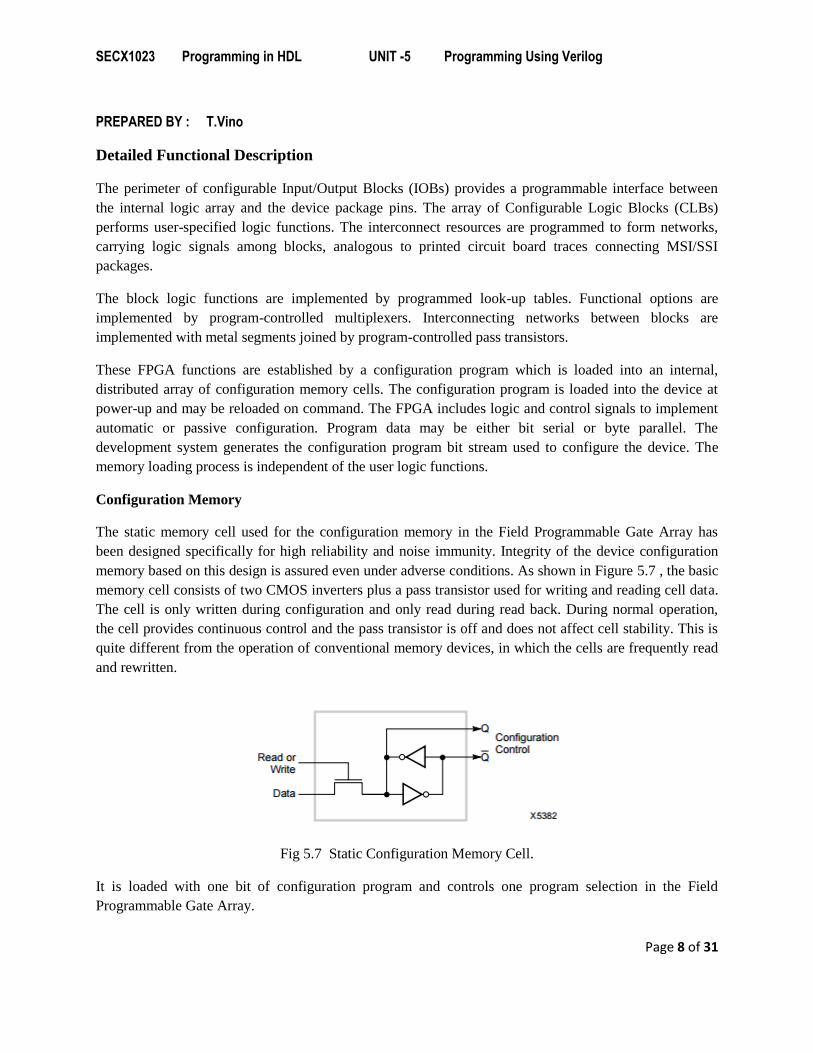
memory based on this design is assured even under adverse conditions. As shown in Figure 5.7 , the basic
memory cell consists of two CMOS inverters plus a pass transistor used for writing and reading cell data.
The cell is only written during configuration and only read during read back. During normal operation,
the cell provides continuous control and the pass transistor is off and does not affect cell stability. This is
quite different from the operation of conventional memory devices, in which the cells are frequently read
and rewritten.
Fig 5.7 Static Configuration Memory Cell.
It is loaded with one bit of configuration program and controls one program selection in the Field
Programmable Gate Array.

SECX1023 Programming in HDL UNIT -5 Programming Using Verilog
PREPARED BY : T.Vino
Page 9 of 31
The memory cell outputs Q and Q’ use ground and VCC levels and provide continuous, direct control.
The additional capacitive load together with the absence of address decoding and sense amplifiers provide
high stability to the cell. Due to the structure of the configuration memory cells, they are not affected by
extreme power-supply excursions or very high levels of alpha particle radiation. In reliability testing, no
soft errors have been observed even in the presence of very high doses of alpha radiation.
The method of loading the configuration data is selectable. Two methods use serial data, while three use
byte-wide data. The internal configuration logic utilizes framing information, embedded in the program
data by the development system, to direct memory-cell loading. The serial-data framing and length-count
preamble provide programming compatibility for mixes of various FPGA device devices in a
synchronous, serial, daisy-chain fashion.
I/O Block
Each user-configurable IOB shown in Figure 5.8 , provides an interface between the external package pin
of the device and the internal user logic. Each IOB includes both registered and direct input paths. Each
IOB provides a programmable 3-state output buffer, which may be driven by a registered or direct output
signal. Configuration options allow each IOB an inversion, a controlled slew rate and a high impedance
pull-up. Each input circuit also provides input clamping diodes to provide electrostatic protection, and
circuits to inhibit latch-up produced by input currents.

SECX1023 Programming in HDL UNIT -5 Programming Using Verilog
PREPARED BY : T.Vino
Page 10 of 31
Fig 5.8 Input/Output Block.
Each IOB includes input and output storage elements and I/O options selected by configuration memory
cells. A choice of two clocks is available on each die edge. The polarity of each clock line (not each flip-
flop or latch) is programmable. A clock line that triggers the flip-flop on the rising edge is an active Low
Latch Enable (Latch transparent) signal and vice versa. Passive pull-up can only be enabled on inputs, not
on outputs. All user inputs are programmed for TTL or CMOS thresholds.
Summary of I/O Options
• Inputs
- Direct
- Flip-flop/latch
- CMOS/TTL threshold (chip inputs)
- Pull-up resistor/open circuit
• Outputs

SECX1023 Programming in HDL UNIT -5 Programming Using Verilog
PREPARED BY : T.Vino
Page 11 of 31
- Direct/registered
- Inverted/not
- 3-state/on/off
- Full speed/slew limited
- 3-state/output enable (inverse)
Configurable Logic Block
The array of CLBs provides the functional elements from which the user’s logic is constructed. The logic
blocks are arranged in a matrix within the perimeter of IOBs. For example, the XC3020A has 64 such
blocks arranged in 8 rows and 8 columns. The development system is used to compile the configuration
data which is to be loaded into the internal configuration memory to define the operation and
interconnection of each block. User definition of CLBs and their interconnecting networks may be done
by automatic translation from a schematic-capture logic diagram or optionally by installing library or user
macros. Each CLB has a combinatorial logic section, two flip-flops, and an internal control section. In
Figure 5.9, There are: five logic inputs (A, B, C, D and E); a common clock input (K); an asynchronous
direct RESET input (RD); and an enable clock (EC). All may be driven from the interconnect resources
adjacent to the blocks. Each CLB also has two outputs (X and Y) which may drive interconnect networks.
Fig 5.9 Configurable Logic Block

SECX1023 Programming in HDL UNIT -5 Programming Using Verilog
PREPARED BY : T.Vino
Page 12 of 31
Each CLB includes a combinatorial logic section, two flip-flops and a program memory controlled
multiplexer selection of function. It has the following:
- five logic variable inputs A, B, C, D, and E
- a direct data in DI
- an enable clock EC
- a clock (invertible) K
- an asynchronous direct RESET RD
- two outputs X and Y

SECX1023 Programming in HDL UNIT -5 Programming Using Verilog
PREPARED BY : T.Vino
Page 13 of 31
Altera Complex Programmable Logic devices
Altera has developed three families of chips that fit within the CPLD category: MAX 5000, MAX 7000,
and MAX 9000. Here, the discussion will focus on the MAX 7000 series, because it is widely used and
offers state-of-the-art logic capacity and speed-performance. MAX 5000 represents an older technology
that offers a cost effective solution, and MAX 9000 is similar to MAX 7000, except that MAX 9000
offers higher logic capacity (the industry’s highest for CPLDs).
The general architecture of the Altera MAX 7000 series is depicted in Figure 5.10 . It comprises an array
of blocks called Logic Array Blocks (LABs), and interconnect wires called a Program mable Interconnect
Array (PIA). The PIA is capable of connecting any LAB input or output to any other LAB. Also, the
inputs and outputs of the chip connect directly to the PIA and to LABs. A LAB can be thought of as a
complex SPLD-like structure, and so the entire chip can be considered to be an array of SPLDs. MAX
7000 devices are available both based in EPROM and EEPROM technology. Until recently, even with
EEPROM, MAX 7000 chips could be programmable only “out-of-circuit” in a special-purpose
programming unit; however, in 1996 Altera released the 7000S series, which is reprogrammable “in-
circuit”.
Fig 5.10 Altera MAX 7000 Series.
The structure of a LAB is shown in Figure 5.11. Each LAB consists of two sets of eight macro cells
(shown in Figure 5.12 ), where a macro cell comprises a set of programmable product terms (part of an
AND-plane) that feeds an OR-gate and a flip-flop. The flip-flops can be configured as D type, JK, T, SR,
or can be transparent. As illustrated in Figure 10, the number of inputs to the OR-gate in a macro cell is
variable; the OR-gate can be fed from any or all of the five product terms within the macro cell, and in
addition can have up to 15 extra product terms from macro cells in the same LAB. This product term
flexibility makes the MAX 7000 series LAB more efficient in terms of chip area because typical logic
functions do not need more than five product terms, and the architecture supports wider functions when

SECX1023 Programming in HDL UNIT -5 Programming Using Verilog
PREPARED BY : T.Vino
Page 14 of 31
they are needed. It is interesting to note that variable sized OR-gates of this sort are not available in basic
SPLDs .
Fig 5.11 Altera MAX 7000 Logic Array Block (LAB).

SECX1023 Programming in HDL UNIT -5 Programming Using Verilog
PREPARED BY : T.Vino
Page 15 of 31
Fig 5.12 MAX 7000 Macro cell.
Altera FLASHlogic CPLDs
Altera’s FLASHlogic, previously known as Intel’s FLEXlogic, features in-system programmability and
provides on-chip SRAM blocks, a unique feature among CPLD products. The upper part of Figure 5.13
illustrates the architecture of FLASHlogic devices; it comprises a collection of PALlike blocks, called
Configurable Function Blocks (CFBs), that each represents an optimized 24V10 PAL.

SECX1023 Programming in HDL UNIT -5 Programming Using Verilog
PREPARED BY : T.Vino
Page 16 of 31
Fig 5.13 Altera FLASHlogic CPLD.
In terms of basic structure, FLASH logic is similar to other products already discussed. However, they
have one unique feature that stands them apart from all other CPLDs: each PAL-like block, instead of
being used for AND-OR logic, can be configured as a block of 10 nsec Static RAM. This concept is
illustrated in the lower part of Figure 5.13, which shows one CFB being used as a PAL and another
configured as an SRAM. In the SRAM configuration, the PAL block becomes a 128 word by 10 bit
read/write memory. Inputs that would normally feed the AND plane in the PAL in this case become
address lines, data in, and control signals for the memory. Notice that the flip-flops and tri-state buffers
are still available when the PAL block is configured as memory. In the FLASH logic device, the AND-
OR logic plane’s configuration bits are SRAM cells that are “shadowed” by EPROM or EEPROM cells.
The SRAM cells are loaded with a copy of the non-volatile EPROM or EEPROM memory when power is
applied, but it is the SRAM cells that control the configuration of the chip. It is possible to re-configure
the chips in-system by downloading new information into the SRAM cells. The SRAM cells’ contents
can be written back to the EEPROM, so that non-volatile re-programming (in-circuit) is available.

SECX1023 Programming in HDL UNIT -5 Programming Using Verilog
PREPARED BY : T.Vino
Page 17 of 31
Interfacing Memory To a Microprocessor Bus
In order to design the interface, the timing specifications for both the memory and
microprocessor must be satisfied. When writing to memory, the setup and hold time
specifications for the memory must be satisfied, and when reading from memory, the
setup and hold time specifications for the microprocessor bus must be satisfied. If the
memory is slow, it may be necessary to insert wait states in the bus cycle.
We design the interface between a 486 bus and a small static RAM memory, and
then we write code to test the interface timing. We use the static RAM and 486
bus interface models that we have already developed. Figure shows how the bus
interface is connected to the static RAM memory.
The memory consists of four static RAM chips, and each RAM chip contains
= 32,768 8-bit words. The four chips operate in parallel to give a memory that is 32 bits
wide. Data bits 31-24 are connected to the first chip, bits 23-16 to the second chip, etc.
The lower 15 bits of the address bus are connected in parallel to all four chips. The
system includes a memory controller that generates WE and CS signals for the memory
and returns a Rdy signal to the bus interface to indicate completion of a read or write
bus cycle. We will assign the address range 0 through 32,767 to the static RAM. In
general, a complete 486 system would have a large dynamic RAM memory and I/O
interface cards connected to the address and data busses. To allow for expansion to
the system, we use an address decoder, so the static RAM is selected only for the
specified address range. When an address in the range 0 to 32,767 is detected, the
decoder outputs CSI = 1, which activates the memory controller.

SECX1023 Programming in HDL UNIT -5 Programming Using Verilog
PREPARED BY : T.Vino
Page 18 of 31
Fig 5.14 Interfacing Memory to a Microprocessor Bus

SECX1023 Programming in HDL UNIT -5 Programming Using Verilog
PREPARED BY : T.Vino
Page 19 of 31
Design of a UART
A UART (Universal Asynchronous Receiver and Transmitter) is a device allowing the reception and
transmission of information, in a serial and asynchronous way
A UART allows the communication between a computer and several kinds of devices (printer, modem,
etc), interconnected via an RS-232 cable
Fig 5.15 Block Diagram
Serial transmission
Data transmission is made by the UART in a serial way, by 11-bit blocks:
• a 0 bit marks the starting point of the block
• eight bits for data
• one parity bit
• a 1 bit marking the end of the block
• The transmission and reception lines should hold a 1 when no data is transmitted
Fig 5.16 Data Transmission in UART
SECX1023 Programming in HDL UNIT -5 Programming Using Verilog
PREPARED BY : T.Vino
Page 20 of 31
The first transmitted bit is the LSB (least significant bit)
The parity bit is set to 1 or 0, depending on the number of 1's transmitted: if even parity is used,
this number should be even; if odd parity is used, this number should be odd. If the chosen parity
is not respected in the block, a transmission error should be detected
The transmission speed is fixed, measured in bauds
Implementation
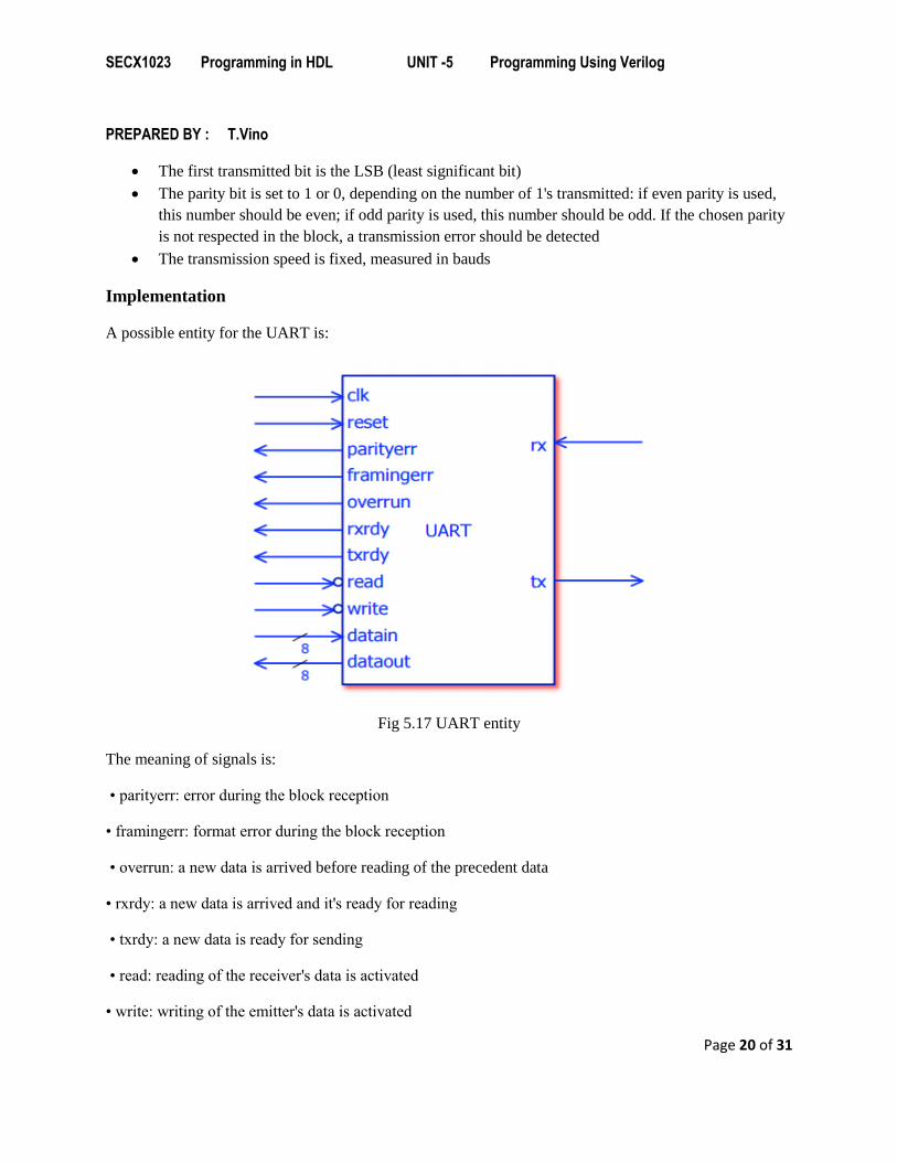
A possible entity for the UART is:
Fig 5.17 UART entity
The meaning of signals is:
• parityerr: error during the block reception
• framingerr: format error during the block reception
• overrun: a new data is arrived before reading of the precedent data
• rxrdy: a new data is arrived and it's ready for reading
• txrdy: a new data is ready for sending
• read: reading of the receiver's data is activated
• write: writing of the emitter's data is activated

SECX1023 Programming in HDL UNIT -5 Programming Using Verilog
PREPARED BY : T.Vino
Page 21 of 31
• data: 8-bit data, read or written
• tx: output bit
• rx: input bit
The UART can be divided into two modules: the receiver and the emitter
Fig 5.18 UART Module
Data emission:
• to test if signal txrdy is active. If yes, a 8-bit data can be written in the emitter
• to place the 8-bit data in the input and to active the write signal
• the UART sends the 8 bits, via the tx signal. During transmission, the txrdy signal should be inactive
• at the end of the emission, txrdy should be active again et tx set to 1
Data reception:
• the 8 bits of information arrive in a serial way, at any moment, via the rx signal. The starting point is
given par a 0 value of rx
• the UART places the 8 bits in a parallel way over dataout, and announces their availability setting rxrdy
active
• the information reading is made active with the read signal

SECX1023 Programming in HDL UNIT -5 Programming Using Verilog
PREPARED BY : T.Vino
Page 22 of 31
Static RAM Memory
Random Access Memory (RAM ) is a form of computer data storage. A random-access memory device
allows data items to be read or written in almost the same amount of time irrespective of the physical
location of data inside the memory. In contrast, with other direct-access data storage media such as hard
disks, CD-RWs, DVD-RWs and the older drum memory, the time required to read and write data items
varies significantly depending on their physical locations on the recording medium, due to mechanical
limitations such as media rotation speeds and arm movement.
RAM contains multiplexing and de-multiplexing circuitry, to connect the data lines to the addressed
storage for reading or writing the entry. Usually more than one bit of storage is accessed by the same
address, and RAM devices often have multiple data lines and are said to be '8-bit' or '16-bit' etc. devices.
In today's technology, random-access memory takes the form of integrated circuits. RAM is normally
associated with volatile types of memory (such as DRAM memory modules), where stored information is
lost if power is removed, although many efforts have been made to develop non-volatile RAM
chips. Other types of non-volatile memories exist that allow random access for read operations, but either
do not allow write operations or have other kinds of limitations on them. These include most types
of ROM and a type of flash memory called NOR-Flash.
The two widely used forms of modern RAM are static RAM (SRAM) and dynamic RAM (DRAM). In
SRAM, a bit of data is stored using the state of a six transistor memory cell. This form of RAM is more
expensive to produce, but is generally faster and requires less dynamic power than DRAM. In modern
computers, SRAM is often used as cache memory for the CPU. DRAM stores a bit of data using a
transistor and capacitor pair, which together comprise a DRAM memory cell. The capacitor holds a high
or low charge (1 or 0, respectively), and the transistor acts as a switch that lets the control circuitry on the
chip read the capacitor's state of charge or change it. As this form of memory is less expensive to produce
than static RAM, it is the predominant form of computer memory used in modern computers.
Both static and dynamic RAM are considered volatile, as their state is lost or reset when power is
removed from the system. By contrast, read-only memory (ROM) stores data by permanently enabling or
disabling selected transistors, such that the memory cannot be altered. Writeable variants of ROM (such
as EEPROM and flash memory) share properties of both ROM and RAM, enabling data to persist without

SECX1023 Programming in HDL UNIT -5 Programming Using Verilog
PREPARED BY : T.Vino
Page 23 of 31
power and to be updated without requiring special equipment. Static Random Access Memory (Static
RAM or SRAM) is a type of RAM that holds data in a static form, that is, as long as the memory has
power. Unlike dynamic RAM, it does not need to be refreshed. SRAM stores a bit of data on four
transistors using two cross-coupled inverters. The two stable states characterize 0 and 1. During read and
write operations another two access transistors are used to manage the availability to a memory cell. To
store one memory bit it requires six metal-oxide-semiconductor field- effect transistors (MOFSET). The
term static differentiates SRAM from DRAM (dynamic random access memory) which must be
periodically refreshed. SRAM is faster and more expensive than DRAM; it is typically used for CPU
cache while DRAM is used for a computer's main memory.
Verilog Code for Static RAM Memory:
Fig 5.19 Static RAM Memory
module ram(clk, wr_en, data_in, addr, data_out);
input clk;
input wr_en;
input [7:0] data_in;
input [3:0] addr;
output [7:0] data_out;
reg [7:0] data_out;
reg [7:0]mem [0:15];
always@(posedge(clk),wr_en,data_in,addr)

SECX1023 Programming in HDL UNIT -5 Programming Using Verilog
PREPARED BY : T.Vino
Page 24 of 31
if(clk)
begin
if(wr_en)
mem[addr]=data_in;
else
data_out=mem[addr];
end
endmodule
CMOS SRAM cell:
Fig 5.20 (a) Six-Transistor CMOS SRAM cell (b) Four Transistor SRAM cell.
A typical SRAM cell is made up of six MOSFETs. Each bit in an SRAM is stored on
four transistors (M1, M2, M3, M4) that form two cross-coupled inverters. This storage cell has two stable
states which are used to denote 0 and 1. Two additional access transistors serve to control the access to a
storage cell during read and write operations. In addition to such six-transistor (6T) SRAM, other kinds of
SRAM chips use 4, 8, 10 (4T, 8T, 10T SRAM), or more transistors per bit. Four-transistor SRAM is quite
common in stand-alone SRAM devices (as opposed to SRAM used for CPU caches), implemented in
special processes with an extra layer of polysilicon, allowing for very high-resistance pull-up
resistors.[8] The principal drawback of using 4T SRAM is increased static powerdue to the constant
current flow through one of the pull-down transistors. This is sometimes used to implement more than

SECX1023 Programming in HDL UNIT -5 Programming Using Verilog
PREPARED BY : T.Vino
Page 25 of 31
one (read and/or write) port, which may be useful in certain types of video memoryand register
files implemented with multi-ported SRAM circuitry.
Generally, the fewer transistors needed per cell, the smaller each cell can be. Since the cost of processing
a silicon wafer is relatively fixed, using smaller cells and so packing more bits on one wafer reduces the
cost per bit of memory.
Memory cells that use fewer than four transistors are possible – but, such 3T or 1T cells are DRAM, not
SRAM (even the so-called 1T-SRAM).
Access to the cell is enabled by the word line (WL in figure) which controls the two access transistors
M5 and M6 which, in turn, control whether the cell should be connected to the bit lines: BL and BL. They
are used to transfer data for both read and write operations. Although it is not strictly necessary to have
two bit lines, both the signal and its inverse are typically provided in order to improve noise margins.
During read accesses, the bit lines are actively driven high and low by the inverters in the SRAM cell.
This improves SRAM bandwidth compared to DRAMs – in a DRAM, the bit line is connected to storage
capacitors and charge sharing causes the bitline to swing upwards or downwards. The symmetric structure
of SRAMs also allows for differential signaling, which makes small voltage swings more easily
detectable. Another difference with DRAM that contributes to making SRAM faster is that commercial
chips accept all address bits at a time. By comparison, commodity DRAMs have the address multiplexed
in two halves, i.e. higher bits followed by lower bits, over the same package pins in order to keep their
size and cost down.
The size of an SRAM with m address lines and n data lines is 2m words, or 2m × n bits. The most common
word size is 8 bits, meaning that a single byte can be read or written to each of 2m different words within
the SRAM chip. Several common SRAM chips have 11 address lines (thus a capacity of 2m = 2,048 = 2k
words) and an 8-bit word, so they are referred to as "2k × 8 SRAM".
SRAM Operation:
An SRAM cell has three different states: standby (the circuit is idle), reading (the data has been
requested) or writing (updating the contents). SRAM operating in read mode and write modes should
have "readability" and "write stability", respectively. The three different states work as follows:

SECX1023 Programming in HDL UNIT -5 Programming Using Verilog
PREPARED BY : T.Vino
Page 26 of 31
Standby
If the word line is not asserted, the access transistors M5 and M6 disconnect the cell from the bit
lines. The two cross-coupled inverters formed by M1 – M4 will continue to reinforce each other as
long as they are connected to the supply.
Reading
In theory, reading only requires asserting the word line WL and reading the SRAM cell state by a
single access transistor and bit line, e.g. M6, BL. Nevertheless, bit lines are relatively long and
have large parasitic capacitance. To speed up reading, a more complex process is used in practice:
The read cycle is started by precharging both bit lines BL and BL, i.e., driving the bit lines to a
threshold voltage (midrange voltage between logical 1 and 0) by an external module. Then
asserting the word line WL enables both the access transistors M5 and M6, which causes the bit
line BL voltage to either slightly drop (bottom NMOS transistor M3 is ON and top PMOS
transistor M4 is off) or rise (top PMOS transistor M4 is on). It should be noted that if BL voltage
rises, the BL voltage drops, and vice versa. Then the BL and BL lines will have a small voltage
difference between them. A sense amplifier will sense which line has the higher voltage and thus
determine whether there was 1 or 0 stored. The higher the sensitivity of the sense amplifier, the
faster the read operation.
Writing
The write cycle begins by applying the value to be written to the bit lines. If we wish to write a 0,
we would apply a 0 to the bit lines, i.e. setting BL to 1 and BL to 0. This is similar to applying a
reset pulse to an SR-latch, which causes the flip flop to change state. A 1 is written by inverting
the values of the bit lines. WL is then asserted and the value that is to be stored is latched in. This
works because the bit line input-drivers are designed to be much stronger than the relatively weak
transistors in the cell itself so they can easily override the previous state of the cross-coupled
inverters. In practice, access NMOS transistors M5 and M6 have to be stronger than either bottom
NMOS (M1, M3) or top PMOS (M2, M4) transistors. This is easily obtained as PMOS transistors
are much weaker than NMOS when same sized. Consequently when one transistor pair (e.g.
M3 and M4) is only slightly overriden by the write process, the opposite transistors pair (M1 and
M2) gate voltage is also changed. This means that the M1 and M2transistors can be easier
overriden, and so on. Thus, cross-coupled inverters magnify the writing process.

SECX1023 Programming in HDL UNIT -5 Programming Using Verilog
PREPARED BY : T.Vino
Page 27 of 31
Design of Microcontroller CPU
Fig 5.21 Basic Microcontroller Block Diagram
CPU is the brain of any processing device. It monitors and controls all operations that are performed in
the Microcontroller.
8051 Internal Architecture:
ALU is main computational block of CPU of the Microcontroller. An arithmetic logic unit (ALU) is
a combinational digital electronic circuit that performs arithmetic and bitwise operations on integerbinary
numbers. This is in contrast to a floating-point unit (FPU), which operates on floating point numbers. An
ALU is a fundamental building block of many types of computing circuits, including the central
processing unit (CPU) of computers and controllers, FPUs, and graphics processing units (GPUs). A
single CPU, FPU or GPU may contain multiple ALUs.

SECX1023 Programming in HDL UNIT -5 Programming Using Verilog
PREPARED BY : T.Vino
Page 28 of 31
Fig 5.21 Intel 8051 Microcontroller Internal Architecture
An arithmetic-logic unit (ALU) is the part of a computer processor (CPU) that carries out arithmetic and
logic operations on the operands in computer instruction words. In some processors, the ALU is divided
into two units, an arithmetic unit (AU) and a logic unit (LU). Some processors contain more than one AU
- for example, one for fixed-point operations and another for floating-point operations. (In personal
computers floating point operations are sometimes done by a floating point unit on a separate chip called
a numeric coprocessor.)

SECX1023 Programming in HDL UNIT -5 Programming Using Verilog
PREPARED BY : T.Vino
Page 29 of 31
Typically, the ALU has direct input and output access to the processor controller, main memory (random
access memory or RAM in a personal computer), and input/output devices. Inputs and outputs flow along
an electronic path that is called a bus. The input consists of an instruction word (sometimes called a
machine instruction word) that contains an operation code (sometimes called an "op code"), one or more
operands, and sometimes a format code. The operation code tells the ALU what operation to perform and
the operands are used in the operation. (For example, two operands might be added together or compared
logically.) The format may be combined with the op code and tells, for example, whether this is a fixed-
point or a floating-point instruction. The output consists of a result that is placed in a storage register and
settings that indicate whether the operation was performed successfully. (If it isn't, some sort of status will
be stored in a permanent place that is sometimes called the machine status word.)
In general, the ALU includes storage places for input operands, operands that are being added, the
accumulated result (stored in an accumulator), and shifted results. The flow of bits and the operations
performed on them in the subunits of the ALU is controlled by gated circuits. The gates in these circuits
are controlled by a sequence logic unit that uses a particular algorithm or sequence for each operation
code. In the arithmetic unit, multiplication and division are done by a series of adding or subtracting and
shifting operations. There are several ways to represent negative numbers. In the logic unit, one of 16
possible logic operations can be performed - such as comparing two operands and identifying where bits
don't match.

SECX1023 Programming in HDL UNIT -5 Programming Using Verilog
PREPARED BY : T.Vino
Page 30 of 31
Verilog Code for ALU:
Fig 5.22 Arithmetic-Logic Unit
TRUTH TABLE:

SECX1023 Programming in HDL UNIT -5 Programming Using Verilog
PREPARED BY : T.Vino
Page 31 of 31
module alu(a, b, cin, s, y);
input [7:0] a;
input [7:0] b;
input cin;
input [3:0] s;
output [7:0] y;
reg [7:0]y;
always @ (a or b or s)
begin
case(s)
4'b0000: y=a;
4'b0001: y=a+1;
4'b0010: y=a-1;
4'b0011: y=b;
4'b0100: y=b+1;
4'b0101: y=b-1;
4'b0110: y=a+b;
4'b0111: y=a+b+cin;
4'b1000: y=~a;
4'b1001: y=~b;
4'b1010: y=a&b;
4'b1011: y=a|b;
4'b1100: y=~(a&b);
4'b1101: y=~(a|b);
4'b1110: y=a^b;
4'b1111: y=~(a^b);
endcase
end
endmodule
_________________________________________________________________