realtek confidential files the document authorized to confidential files the document authorized to...
TRANSCRIPT
Realtek confidential files
The document authorized to
T&W
2010-07-02 17:17:51
RTL8196C-GR
IEEE 802.11n AP/ROUTER NETWORK PROCESSOR WITH EEE
DATASHEET (CONFIDENTIAL: Development Partners Only)
Rev. 1.2 23 March 2010
Track ID: JATR-2265-11
Realtek Semiconductor Corp. No. 2, Innovation Road II, Hsinchu Science Park, Hsinchu 300, Taiwan Tel.: +886-3-578-0211. Fax: +886-3-577-6047 www.realtek.com
www.DataSheet.net/
Datasheet pdf - http://www.DataSheet4U.co.kr/
Realtek confidential files
The document authorized to
T&W
2010-07-02 17:17:51
RTL8196C Datasheet
IEEE 802.11n AP/Router Network Processor with EEE ii Track ID: JATR-2265-11 Rev. 1.2
COPYRIGHT ©2010 Realtek Semiconductor Corp. All rights reserved. No part of this document may be reproduced, transmitted, transcribed, stored in a retrieval system, or translated into any language in any form or by any means without the written permission of Realtek Semiconductor Corp.
DISCLAIMER Realtek provides this document “as is”, without warranty of any kind. Realtek may make improvements and/or changes in this document or in the product described in this document at any time. This document could include technical inaccuracies or typographical errors.
TRADEMARKS Realtek is a trademark of Realtek Semiconductor Corporation. Other names mentioned in this document are trademarks/registered trademarks of their respective owners.
USING THIS DOCUMENT This document provides detailed user guidelines to achieve the best performance when implementing the RTL8196C.
Though every effort has been made to ensure that this document is current and accurate, more information may have become available subsequent to the production of this guide.
REVISION HISTORY Revision Release Date Summary
1.1 2010/03/18 First release. 1.2 2010/03/23 Revised IEEE 802.3az draft version from Draft 2.0 to Draft 2.3.
Revised Figure 3 One 16-bit, for 1M/2M/4M/8M Bytes Flash Configuration, page 12.
www.DataSheet.net/
Datasheet pdf - http://www.DataSheet4U.co.kr/
Realtek confidential files
The document authorized to
T&W
2010-07-02 17:17:51
RTL8196C Datasheet
IEEE 802.11n AP/Router Network Processor with EEE iii Track ID: JATR-2265-11 Rev. 1.2
Table of Contents 1. GENERAL DESCRIPTION..............................................................................................................................................1 2. FEATURES.........................................................................................................................................................................2 3. BLOCK DIAGRAM...........................................................................................................................................................4 4. PIN ASSIGNMENTS .........................................................................................................................................................5
4.1. PIN ASSIGNMENTS .......................................................................................................................................................5 4.2. PACKAGE IDENTIFICATION...........................................................................................................................................5
5. PIN DESCRIPTIONS.........................................................................................................................................................6 5.1. RTL8196C CONFIGURATION UPON POWER ON STRAPPING ........................................................................................9 5.2. SHARED I/O PIN MAPPING .........................................................................................................................................10
6. MEMORY CONTROLLER............................................................................................................................................11 6.1. SDRAM CONTROL INTERFACE..................................................................................................................................11
6.1.1. Features................................................................................................................................................................11 6.2. NOR FLASH TYPE MEMORY......................................................................................................................................11
6.2.1. Features................................................................................................................................................................11 6.2.2. Bank Address Mapping.........................................................................................................................................12 6.2.3. Flash Command Sequence....................................................................................................................................12
6.3. SPI FLASH CONTROLLER ...........................................................................................................................................13 6.3.1. Features................................................................................................................................................................13
6.4. SOFTWARE REGISTER DEFINITION .............................................................................................................................13 6.4.1. Memory Control Register (MCR) (0xB800_1000) ...............................................................................................13 6.4.2. DRAM Configuration Register (DCR) (0xB800_1004)........................................................................................14 6.4.3. DRAM Timing Register (DTR) (0xB800_1008)....................................................................................................15 6.4.4. NOR Flash Configuration Register (NFCR) (0xB800_1100)...............................................................................16 6.4.5. SPI Flash Configuration Register (SFCR) (0xB800_1200)..................................................................................16 6.4.6. SPI Flash Configuration Register 2 (SFCR2) (0xB800_1204).............................................................................17 6.4.7. SPI Flash Control and Status Register (SFCSR) (0xB800_1208) ........................................................................18 6.4.8. SPI Flash Data Register (SFDR) (0xB800_120C) ...............................................................................................18 6.4.9. SPI Flash Data Register 2 (SFDR2) (0xB800_1210)...........................................................................................19
7. PERIPHERAL AND MISC CONTROL ........................................................................................................................20 7.1. GPIO CONTROL .........................................................................................................................................................20
7.1.1. GPIO Register Set (0xB800_3500).......................................................................................................................20 7.1.2. GPIO Port A, B, C, D Control Register (PABCD_CNR) (0xB800_3500)............................................................20 7.1.3. GPIO Port A, B, C, D Direction Register (PABCD_DIR) (0xB800_3508)..........................................................21 7.1.4. Port A, B, C, D Data Register (PABCD_DAT) (0xB800_350C) ..........................................................................21 7.1.5. Port A, B, C, D Interrupt Status Register (PABCD_ISR) (0xB800_3510) ...........................................................21 7.1.6. Port A, B Interrupt Mask Register (PAB_IMR) (0xB800_3514) ..........................................................................22 7.1.7. Port C, D Interrupt Mask Register (PCD_IMR) (0xB800_3518).........................................................................22
7.2. GPIO SHARED PIN MAPPING LIST .............................................................................................................................23 7.2.1. Shared Pin Register (PIN_MUX_SEL) (0xB800_0040) .......................................................................................23 7.2.2. Shared Pin Register (PIN_MUX_SEL2) (0xB800_003C) ....................................................................................24
8. GREEN ETHERNET.......................................................................................................................................................25 8.1. CABLE LENGTH POWER SAVING ................................................................................................................................25 8.2. LINK DOWN POWER SAVING......................................................................................................................................25 8.3. ENERGY EFFICIENT ETHERNET (EEE)........................................................................................................................25
www.DataSheet.net/
Datasheet pdf - http://www.DataSheet4U.co.kr/

Realtek confidential files
The document authorized to
T&W
2010-07-02 17:17:51
RTL8196C Datasheet
IEEE 802.11n AP/Router Network Processor with EEE iv Track ID: JATR-2265-11 Rev. 1.2
9. DC SPECIFICATIONS....................................................................................................................................................26 9.1. OPERATING CONDITIONS ...........................................................................................................................................26 9.2. POWER DISSIPATION ..................................................................................................................................................26 9.3. SDRAM BUS DC PARAMETERS ................................................................................................................................27 9.4. FLASH BUS DC PARAMETERS ....................................................................................................................................27 9.5. USB 1.1 DC PARAMETERS.........................................................................................................................................28 9.6. USB 2.0 DC PARAMETERS.........................................................................................................................................28 9.7. UART DC PARAMETERS ...........................................................................................................................................28 9.8. GPIO DC PARAMETERS.............................................................................................................................................29 9.9. JTAG DC PARAMETERS ............................................................................................................................................29 9.10. LED DC PARAMETERS ..............................................................................................................................................29
10. AC SPECIFICATIONS...............................................................................................................................................30 10.1. CLOCK SIGNAL TIMING..............................................................................................................................................30
10.1.1. SDRAM Clock Timing......................................................................................................................................31 10.2. BUS SIGNAL TIMING ..................................................................................................................................................32
10.2.1. SDRAM Bus .....................................................................................................................................................32 10.2.2. Flash Bus .........................................................................................................................................................34 10.2.3. Power Sequence...............................................................................................................................................34 10.2.4. Power Configuration Timing ...........................................................................................................................35
11. THERMAL CHARACTERISTICS ...........................................................................................................................36 11.1. THERMAL OPERATING RANGE ...................................................................................................................................37 11.2. RTL8196C THERMAL PARAMETERS..........................................................................................................................37
12. MECHANICAL DIMENSIONS.................................................................................................................................38 12.1. PLASTIC QUAD FLAT PACKAGE 128-PIN 14X20MM OUTLINE....................................................................................38
13. ORDERING INFORMATION...................................................................................................................................39
www.DataSheet.net/
Datasheet pdf - http://www.DataSheet4U.co.kr/

Realtek confidential files
The document authorized to
T&W
2010-07-02 17:17:51
RTL8196C Datasheet
IEEE 802.11n AP/Router Network Processor with EEE v Track ID: JATR-2265-11 Rev. 1.2
List of Tables TABLE 1. PIN DESCRIPTIONS ........................................................................................................................................................6 TABLE 2. RTL8196C CONFIGURATION UPON POWER ON STRAPPING .........................................................................................9 TABLE 3. SHARED I/O PIN MAPPING ..........................................................................................................................................10 TABLE 4. MEMORY CONTROL REGISTER (MCR) (0XB800_1000) .............................................................................................13 TABLE 5. DRAM CONFIGURATION REGISTER (DCR) (0XB800_1004)......................................................................................14 TABLE 6. DRAM TIMING REGISTER (DTR) (0XB800_1008).....................................................................................................15 TABLE 7. NOR FLASH CONFIGURATION REGISTER (NFCR) (0XB800_1100)............................................................................16 TABLE 8. SPI FLASH CONFIGURATION REGISTER (SFCR) (0XB800_1200) ...............................................................................16 TABLE 9. SPI FLASH CONFIGURATION REGISTER 2 (SPCR2) (0XB800_1204) ..........................................................................17 TABLE 10. SPI FLASH CONTROL AND STATUS REGISTER (SFCSR) (0XB800_1208) ..................................................................18 TABLE 11. SPI FLASH DATA REGISTER (SFDR) (0XB800_120C)...............................................................................................18 TABLE 12. SPI FLASH DATA REGISTER 2 (SFDR2) (0XB800_1210)...........................................................................................19 TABLE 13. GPIO REGISTER SET (0XB800_3500)........................................................................................................................20 TABLE 14. GPIO PORT A, B, C, D CONTROL REGISTER (PABCD_CNR) (0XB800_3500) .........................................................20 TABLE 15. GPIO PORT A, B, C, D DIRECTION REGISTER (PABCD_DIR) (0XB800_3508) ........................................................21 TABLE 16. PORT A, B, C, D DATA REGISTER (PABCD_DAT) (0XB800_350C).........................................................................21 TABLE 17. PORT A, B, C, D INTERRUPT STATUS REGISTER (PABCD_ISR) (0XB800_3510)......................................................21 TABLE 18. PORT A, B INTERRUPT MASK REGISTER (PAB_IMR) (0XB800_3514) .....................................................................22 TABLE 19. PORT C, D INTERRUPT MASK REGISTER (PCD_IMR) (0XB800_3518) .....................................................................22 TABLE 20. SHARED PIN REGISTER (PIN_MUX_SEL) (0XB800_0040) ......................................................................................23 TABLE 21. SHARED PIN REGISTER (PIN_MUX_SEL2) (0XB800_003C)....................................................................................24 TABLE 22. OPERATING CONDITIONS ...........................................................................................................................................26 TABLE 23. POWER DISSIPATION ..................................................................................................................................................26 TABLE 24. SDRAM BUS DC PARAMETERS ................................................................................................................................27 TABLE 25. FLASH BUS DC PARAMETERS ....................................................................................................................................27 TABLE 26. USB 1.1 DC PARAMETERS.........................................................................................................................................28 TABLE 27. USB 2.0 DC PARAMETERS.........................................................................................................................................28 TABLE 28. UART DC PARAMETERS ...........................................................................................................................................28 TABLE 29. GPIO DC PARAMETERS.............................................................................................................................................29 TABLE 30. JTAG DC PARAMETERS ............................................................................................................................................29 TABLE 31. LED DC PARAMETERS ..............................................................................................................................................29 TABLE 32. CLOCK SIGNAL TIMING..............................................................................................................................................30 TABLE 33. SDRAM CLOCK TIMING............................................................................................................................................31 TABLE 34. SDRAM INPUT TIMING .............................................................................................................................................32 TABLE 35. SDRAM OUTPUT TIMING..........................................................................................................................................32 TABLE 36. SDRAM ACCESS CONTROL TIMING ..........................................................................................................................33 TABLE 37. FLASH ACCESS TIMING VALUES ................................................................................................................................34 TABLE 38. POWER-UP TIMING PARAMETERS ..............................................................................................................................34 TABLE 39. THERMAL OPERATING RANGE ...................................................................................................................................37 TABLE 40. RTL8196C THERMAL PARAMETERS..........................................................................................................................37 TABLE 41. ORDERING INFORMATION ..........................................................................................................................................39
www.DataSheet.net/
Datasheet pdf - http://www.DataSheet4U.co.kr/

Realtek confidential files
The document authorized to
T&W
2010-07-02 17:17:51
RTL8196C Datasheet
IEEE 802.11n AP/Router Network Processor with EEE vi Track ID: JATR-2265-11 Rev. 1.2
List of Figures FIGURE 1. BLOCK DIAGRAM ........................................................................................................................................................4 FIGURE 2. PIN ASSIGNMENTS .......................................................................................................................................................5 FIGURE 3. ONE 16-BIT, FOR 1M/2M/4M/8M BYTES FLASH CONFIGURATION............................................................................12 FIGURE 4. TYPICAL CONNECTION TO A CRYSTAL ......................................................................................................................30 FIGURE 5. TYPICAL CONNECTION TO AN OSCILLATOR...............................................................................................................30 FIGURE 6. SDRAM CLOCK SPECIFICATIONS-1 ..........................................................................................................................31 FIGURE 7. SDRAM CLOCK SPECIFICATIONS-2 ..........................................................................................................................31 FIGURE 8. SDRAM INPUT TIMING.............................................................................................................................................32 FIGURE 9. SDRAM OUTPUT TIMING .........................................................................................................................................32 FIGURE 10. SDRAM ACCESS CONTROL TIMING.........................................................................................................................33 FIGURE 11. FLASH ACCESS TIMING.............................................................................................................................................34 FIGURE 12. POWER UP SEQUENCE TIMING DIAGRAM .................................................................................................................34 FIGURE 13. POWER UP CONFIGURATION TIMING DIAGRAM........................................................................................................35
www.DataSheet.net/
Datasheet pdf - http://www.DataSheet4U.co.kr/
Realtek confidential files
The document authorized to
T&W
2010-07-02 17:17:51
RTL8196C Datasheet
IEEE 802.11n AP/Router Network Processor with EEE 1 Track ID: JATR-2265-11 Rev. 1.2
1. General Description The RTL8196C is an integrated System-on-a-Chip (SoC) Application Specific Integrated Circuit (ASIC) that implements a basic L2 5-port Ethernet switch and a high performance CPU. The embedded RISC CPU is an RLX4181, and the clock rate can be up to 400MHz. To improve computational performance, a 16-Kbyte I-Cache, 8-Kbyte D-Cache, 16-K I-MEM, and 8-Kbyte D-MEM are provided. A standard 5-signal P1149.1 compliant EJTAG test interface is supported for CPU testing and software development.
The RTL8196C provides five ports (from port 0 to port 4), integrated with five MAC and five physical layer transceivers for 10Base-T and 100Base-TX. Each port of the RTL8196C may be configured as a LAN or WAN port.
The RTL8196C supports flexible IEEE 802.3x full-duplex flow control and optional half-duplex backpressure control. For full-duplex, standard IEEE 803.3x flow control will enable pause ability only when both sides of UTP have auto-negotiation ability and have enabled pause ability. The RTL8196C also provides optional forced mode IEEE 802.3x full-duplex flow control. Based on optimized packet memory management, the RTL8196C is capable of Head-Of-Line blocking prevention.
L2 Switch Features: The RTL8196C contains a 1024-entry address look-up table with a 10-bit 4-way XOR hashing algorithm for address searching and learning. Auto aging of each entry is provided and the aging time is 300~450 seconds.
The RTL8196C supports IEEE 802.3az Draft 2.3, also known as Energy Efficient Ethernet (EEE). IEEE 802.3az operates with the IEEE 802.3 Media Access Control (MAC) Sublayer to support operation in Low Power Idle mode. When the Ethernet network is in low link utilization, EEE allows systems on both sides of the link to save power. Green Ethernet power saving provides: link-on and dynamic detection of cable length, and dynamic adjustment of power required for the detected cable length. This feature provides high performance with minimum power consumption. The RTL8196C also implements link-down power saving on a per-port basis, greatly cutting power consumption when the network cable is disconnected.
For peripheral interfaces, one 16550-compatible UART is supported, and a 16-byte FIFO buffer is provided. A USB 2.0 host controller is embedded in the RTL8196C to provide EHCI and OHCI 1.1 compliant host functionality. A USB PHY is also embedded in the RTL8196C.
An MDI/MDIX auto-crossover function is supported. For accessing high-speed devices, the RTL8196C provides a PCI Express bridge to access a PCI Express interface.
The RTL8196C requires only a single 25MHz crystal or 40MHz clock input for the system PLL. The RTL8196C also has two hardware timers and one watchdog timer to provide accurate timing and watchdog functionality. For extension and flexibility, the RTL8196C has up to 22 GPIO pins.
The RTL8196C is provided in a PQFP 128-pin package. It requires only a 3.3V and 1.0V external power supply.
www.DataSheet.net/
Datasheet pdf - http://www.DataSheet4U.co.kr/
Realtek confidential files
The document authorized to
T&W
2010-07-02 17:17:51
RTL8196C Datasheet
IEEE 802.11n AP/Router Network Processor with EEE 2 Track ID: JATR-2265-11 Rev. 1.2
2. Features
SOC
Embedded RISC CPU, RLX4181 with 16K I-Cache, 8K D-Cache, 16K I-MEM, 8K D-MEM
Supports MIPS-1 ISA, MIPS16 ISA
Clock rate up to 400MHz
Provides a standard 5-signal P1149.1 EJTAG test port
Supports RLX4181 CPU suspend mode
L2 Capabilities
Five Ethernet MAC integrated switch with five 10M/100Mbps physical layers and transceivers for IEEE 802.3 10Base-T and 100Base-TX
Non-blocking wire-speed reception and transmission and non-head-of-line-blocking/forwarding
Internal 512Kbit SRAM for packet buffering
Internal 1024 entry 4-way hash L2 look-up table
Supports source and destination MAC address filtering
Supports IEEE 802.1x port-based and MAC-based Network Access Control
Complies with IEEE 802.3/802.3u/802.1q/802.1d
Flexible full-duplex 802.3x flow control and optional half-duplex backpressure flow control
MAC learning supports Shared VLAN Learning (SVL) and Independent VLAN Learning (IVL) modes
CPU Interface (NIC)
Supports BSD mbuf-like packet structure with adjustable cluster size (128-byte to 2Kbyte) to provide optimum memory utilization
Provides the ‘To-CPU reason’ in the packet header to facilitate packet processing
The NIC DMA supports multiple-descriptor-ring architecture for QoS applications (supports 6 RX descriptor rings and 2 TX descriptor rings)
Peripheral Interfaces
Supports one PCI Express Host with integrated PHY
Supports one 16550 UART
Supports up to 22 GPIO pins
Supports one-port USB 2.0 host interface
Embedded USB PHY
Memory Interfaces
NOR Flash Supports two Flash banks that can be
configured as 8/16-bit bus, 256k/512k /1M/2M/4M/8M bytes
System supports up to 16Mbyte Flash memory space
Boot up from NOR Flash is supported
SPI Flash Supports 4 channels for SPI Flash
application Boot up from SPI Flash is supported System supports up to 32Mbyte Flash
memory space
www.DataSheet.net/
Datasheet pdf - http://www.DataSheet4U.co.kr/
Realtek confidential files
The document authorized to
T&W
2010-07-02 17:17:51
RTL8196C Datasheet
IEEE 802.11n AP/Router Network Processor with EEE 3 Track ID: JATR-2265-11 Rev. 1.2
SDRAM Supports two SDRAM banks that can
be configured as 2M/4M/8M/16M/ 32M/64Mbyte
16-bit SDRAM data bus is supported. System totally supports up to 128Mbyte SDRAM memory space
Supports Green Ethernet
Cable length power saving
Power down power saving
Supports IEEE 802.3az Draft 2.3 Energy Efficient Ethernet (EEE) for 100Base-TX in full duplex operation, and 10Base-T in full/half duplex mode
Other Add-on-Value Features
Supports Link down power saving in Ethernet PHY
Supports two hardware timers and one watchdog timer
Per-port configurable auto-crossover function
Single 25MHz crystal or 40MHz clock input
PQFP 128-pin package
www.DataSheet.net/
Datasheet pdf - http://www.DataSheet4U.co.kr/

Realtek confidential files
The document authorized to
T&W
2010-07-02 17:17:51
RTL8196C Datasheet
IEEE 802.11n AP/Router Network Processor with EEE 4 Track ID: JATR-2265-11 Rev. 1.2
3. Block Diagram
Figure 1. Block Diagram
www.DataSheet.net/
Datasheet pdf - http://www.DataSheet4U.co.kr/

Realtek confidential files
The document authorized to
T&W
2010-07-02 17:17:51
RTL8196C Datasheet
IEEE 802.11n AP/Router Network Processor with EEE 5 Track ID: JATR-2265-11 Rev. 1.2
4. Pin Assignments 4.1. Pin Assignments
RESET#/GPIOB7GPIOC[0]
LED_PORT4/GPIOB6
40M_SEL40M_CLK
VDD33
LED_PORT2/GPIOB4LED_PORT3/GPIOB5
VDD10
25M_XO
VDD10_USB
25M_XI
AVDD33_25M
AGND_PCIEREFCLKPREFCLKN
AVDD10_PCIEHSOPHSON
USB_DNGND
AVDD33_BG
VDD33
MA1
MA8
103
124123122121
125
128127126
113112111110109108107106105104
114
120119118117116115
MA1155
59
56
58
60
57
6261
6364
5453
4748
5049
5152
4344
4645
3940
4241
MA3
MA9
MA12
MA2
MA0MA10MA14/BS1
MA7
MA19/SF_SDIO1/GPIOC[3]MA20/SF_SDIO0/GPIOC[4]
MA4MA21/SF_SCK/GPIOC[5]
MA5MA6
GNDMA17/SF_SDIO3/GPIOC[1]
MA18/SF_SDIO2/GPIOC[2]VDD33
VDD33
VDD10
NF_CS0#/SF_CS0#NF_CS1#/SF_CS1#/MCLKE/GPIOA1
AVDD33_USB_PCIEUSB_DP
HSINHSIP
Figure 2. Pin Assignments
4.2. Package Identification Green package is indicated by a ‘G’ in the location marked ‘T’ in Figure 2.
www.DataSheet.net/
Datasheet pdf - http://www.DataSheet4U.co.kr/

Realtek confidential files
The document authorized to
T&W
2010-07-02 17:17:51
RTL8196C Datasheet
IEEE 802.11n AP/Router Network Processor with EEE 6 Track ID: JATR-2265-11 Rev. 1.2
5. Pin Descriptions In this section the following abbreviations are used:
I: Input AI: Analog Input
O: Output AO: Analog Output
IO: Bi-Directional Input/Output AI/O: Analog Bi-Directional Input/Output
P: Digital Power AP: Analog Power
G: Digital Ground AG: Analog Ground
T/S: Tri-State Bi-Directional Input/Output S/T/S: Sustained Tri-State
IPD: Input Pin With Pull-Down Resistor OOD: Output With Open Drain
IPU: Input Pin With Pull-Up Resistor; (Typical Value = 75K Ohm)
O3S: Output With Tri-State
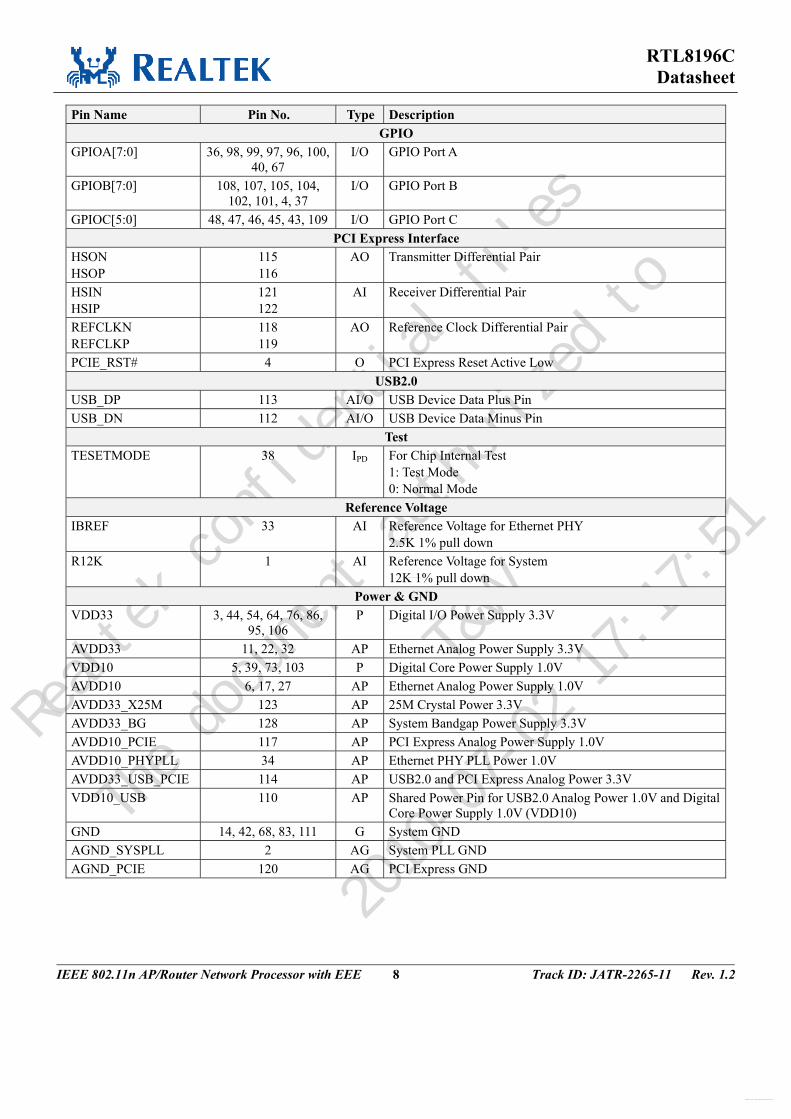
Table 1. Pin Descriptions
Pin Name Pin No. Type Description Clock & Reset
25M_XI 127 I 25MHz Crystal Clock Input 25M_XO 126 O 25MHz Crystal Clock Output 40M_CLK 125 I 40MHz Clock Input Vpeak-to-peak 1.4 Voltage 40M_SEL 124 I System Clock Source Select.
0: 25MHz 1: 40MHz
RESET# 108 I The System Reset Active Low 10M/100Mbps Physical Layer
TXOP[4:0] TXON[4:0]
28, 26, 18, 16, 7 29, 25, 19, 15, 8
AO 10/100M Ethernet Physical Layer Transmit Pair. For differential data transmission
RXIP[4:0] RXIN[4:0]
30, 24, 20, 13, 9 31, 23, 21, 12, 8
AI 10/100M Ethernet Physical Layer Receive Pair. For differential data reception
Memory Bus MD[15:0] 94, 93, 92, 91, 90, 89,
88, 87, 74, 75, 77, 78, 79, 80, 81, 82
I/O Data for SDRAM and NOR Type Flash
MA[21:0] 48, 47, 46, 45, 43, 85, 72, 63, 65, 57, 56, 62, 55, 53, 52, 51, 50, 49,
58, 59, 60, 61
O Address for SDRAM and NOR Type Flash. Shared pins: MA[13]: SDRAM BS0 MA[14]: SDRAM BS1 MA[15]: SDRAM LDQM MA[16]: SDRAM UDQM MA[17]: SPI Flash SDIO3 MA[18]: SPI Flash SDIO2 MA[19]: SPI Flash SDIO1 MA[20]: SPI Flash SDIO0 MA[21]: SPI Flash SCK
www.DataSheet.net/
Datasheet pdf - http://www.DataSheet4U.co.kr/

Realtek confidential files
The document authorized to
T&W
2010-07-02 17:17:51
RTL8196C Datasheet
IEEE 802.11n AP/Router Network Processor with EEE 7 Track ID: JATR-2265-11 Rev. 1.2
Pin Name Pin No. Type Description SDRAM Control
MCLK 84 O SDRAM Clock MCLKE 40 O SDRAM Clock Enable MCS0# 66 O SDRAM Bank 0 Chip Select MCS1# 67 O SDRAM Bank 1 Chip Select BS[1:0] 63, 65 O SDRAM Chip Bank Select [1:0]
Shared with A[14:13] RAS# 69 O Raw Address Strobe for SDRAM CAS# 70 O Column Address Strobe for SDRAM WE# 71 O Write Enable for SDRAM LDQM 72 O Lower Data Mask Output to SDRAM
Corresponds to D[7:0] Pin shared with A[15]
UDQM 85 O Upper Data Mask Output to SDRAM Corresponds to D[15:8] Pin shared with A[16]
NOR Type Flash Control NF_CS0# 41 O ROM Bank 0 Chip Select for NOR Type Flash Memory NF_CS1# 40 O ROM Bank 0 Chip Select for NOR Type Flash Memory OE# 69 O Output Enable (OE#) for NOR Type Flash.
Pin shared with SDRAM RAS# WE# 71 O Write Enable for NOR Type Flash.
Pin shared with SDRAM WE# SPI Serial Flash Control
SF_CS0# 41 O SPI Serial Flash Chip Select 0 Pin shared with NOF_CS0#
SF_CS1# 40 O SPI Serial Flash Chip Select 1 Pin shared with NOF_CS1#
SF_SDIO[3:0] 43, 45, 46, 47 I/O SPI Serial Flash Serial Data Input/Output SF_SCK 48 O SPI Serial Flash Serial Clock Output
The SF_SDI will be driven on the falling edge The SF_SDO will be latched on the rising edge
UART UART_TX 37 O UART Data Transmit Serial Output UART_RX 36 IPD UART Data Receive Serial Input
JTAG JTAG_TCK 100 IPU JTAG Test Clock JTAG_TMS 97 IPU JTAG Test Mode Select JTAG_TDO 98 O JTAG Test Data Output JTAG_TDI 99 IPU JTAG Test Data In JTAG_TRST# 96 IPU JTAG Test Reset
LED LED_PORT[4:0] 107, 105, 104, 102, 101 O Link/Activity Status of 5 Ethernet Ports
www.DataSheet.net/
Datasheet pdf - http://www.DataSheet4U.co.kr/
Realtek confidential files
The document authorized to
T&W
2010-07-02 17:17:51
RTL8196C Datasheet
IEEE 802.11n AP/Router Network Processor with EEE 8 Track ID: JATR-2265-11 Rev. 1.2
Pin Name Pin No. Type Description GPIO
GPIOA[7:0] 36, 98, 99, 97, 96, 100, 40, 67
I/O GPIO Port A
GPIOB[7:0] 108, 107, 105, 104, 102, 101, 4, 37
I/O GPIO Port B
GPIOC[5:0] 48, 47, 46, 45, 43, 109 I/O GPIO Port C PCI Express Interface
HSON HSOP
115 116
AO Transmitter Differential Pair
HSIN HSIP
121 122
AI Receiver Differential Pair
REFCLKN REFCLKP
118 119
AO Reference Clock Differential Pair
PCIE_RST# 4 O PCI Express Reset Active Low USB2.0
USB_DP 113 AI/O USB Device Data Plus Pin USB_DN 112 AI/O USB Device Data Minus Pin
Test TESETMODE 38 IPD For Chip Internal Test
1: Test Mode 0: Normal Mode
Reference Voltage IBREF 33 AI Reference Voltage for Ethernet PHY
2.5K 1% pull down R12K 1 AI Reference Voltage for System
12K 1% pull down Power & GND
VDD33 3, 44, 54, 64, 76, 86, 95, 106
P Digital I/O Power Supply 3.3V
AVDD33 11, 22, 32 AP Ethernet Analog Power Supply 3.3V VDD10 5, 39, 73, 103 P Digital Core Power Supply 1.0V AVDD10 6, 17, 27 AP Ethernet Analog Power Supply 1.0V AVDD33_X25M 123 AP 25M Crystal Power 3.3V AVDD33_BG 128 AP System Bandgap Power Supply 3.3V AVDD10_PCIE 117 AP PCI Express Analog Power Supply 1.0V AVDD10_PHYPLL 34 AP Ethernet PHY PLL Power 1.0V AVDD33_USB_PCIE 114 AP USB2.0 and PCI Express Analog Power 3.3V VDD10_USB 110 AP Shared Power Pin for USB2.0 Analog Power 1.0V and Digital
Core Power Supply 1.0V (VDD10) GND 14, 42, 68, 83, 111 G System GND AGND_SYSPLL 2 AG System PLL GND AGND_PCIE 120 AG PCI Express GND
www.DataSheet.net/
Datasheet pdf - http://www.DataSheet4U.co.kr/
Realtek confidential files
The document authorized to
T&W
2010-07-02 17:17:51
RTL8196C Datasheet
IEEE 802.11n AP/Router Network Processor with EEE 9 Track ID: JATR-2265-11 Rev. 1.2
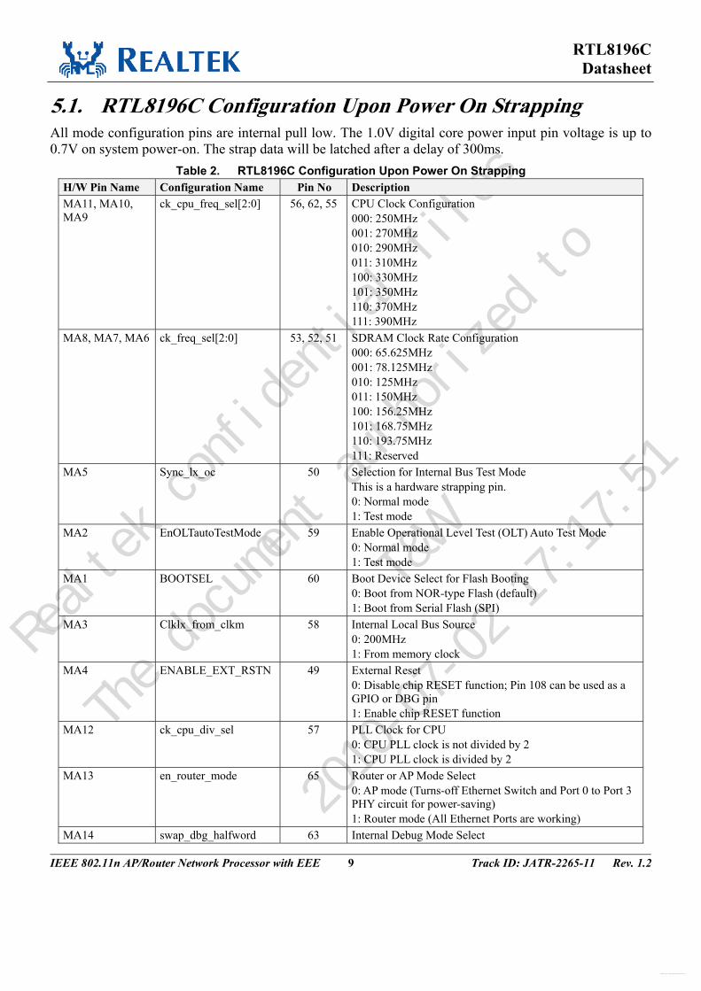
5.1. RTL8196C Configuration Upon Power On Strapping All mode configuration pins are internal pull low. The 1.0V digital core power input pin voltage is up to 0.7V on system power-on. The strap data will be latched after a delay of 300ms.
Table 2. RTL8196C Configuration Upon Power On Strapping H/W Pin Name Configuration Name Pin No Description MA11, MA10, MA9
ck_cpu_freq_sel[2:0] 56, 62, 55 CPU Clock Configuration 000: 250MHz 001: 270MHz 010: 290MHz 011: 310MHz 100: 330MHz 101: 350MHz 110: 370MHz 111: 390MHz
MA8, MA7, MA6 ck_freq_sel[2:0] 53, 52, 51 SDRAM Clock Rate Configuration 000: 65.625MHz 001: 78.125MHz 010: 125MHz 011: 150MHz 100: 156.25MHz 101: 168.75MHz 110: 193.75MHz 111: Reserved
MA5 Sync_lx_oc 50 Selection for Internal Bus Test Mode This is a hardware strapping pin. 0: Normal mode 1: Test mode
MA2 EnOLTautoTestMode 59 Enable Operational Level Test (OLT) Auto Test Mode 0: Normal mode 1: Test mode
MA1 BOOTSEL 60 Boot Device Select for Flash Booting 0: Boot from NOR-type Flash (default) 1: Boot from Serial Flash (SPI)
MA3 Clklx_from_clkm 58 Internal Local Bus Source 0: 200MHz 1: From memory clock
MA4 ENABLE_EXT_RSTN 49 External Reset 0: Disable chip RESET function; Pin 108 can be used as a GPIO or DBG pin 1: Enable chip RESET function
MA12 ck_cpu_div_sel 57 PLL Clock for CPU 0: CPU PLL clock is not divided by 2 1: CPU PLL clock is divided by 2
MA13 en_router_mode 65 Router or AP Mode Select 0: AP mode (Turns-off Ethernet Switch and Port 0 to Port 3 PHY circuit for power-saving) 1: Router mode (All Ethernet Ports are working)
MA14 swap_dbg_halfword 63 Internal Debug Mode Select
www.DataSheet.net/
Datasheet pdf - http://www.DataSheet4U.co.kr/
Realtek confidential files
The document authorized to
T&W
2010-07-02 17:17:51
RTL8196C Datasheet
IEEE 802.11n AP/Router Network Processor with EEE 10 Track ID: JATR-2265-11 Rev. 1.2
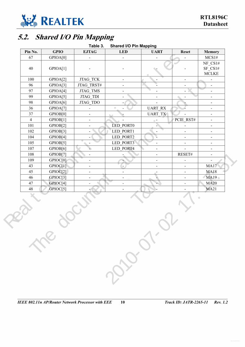
5.2. Shared I/O Pin Mapping Table 3. Shared I/O Pin Mapping
Pin No. GPIO EJTAG LED UART Reset Memory 67 GPIOA[0] - - - - MCS1#
40 GPIOA[1] - - - - NF_CS1# SF_CS1# MCLKE
100 GPIOA[2] JTAG_TCK - - - - 96 GPIOA[3] JTAG_TRST# - - - - 97 GPIOA[4] JTAG_TMS - - - - 99 GPIOA[5] JTAG_TDI - - - - 98 GPIOA[6] JTAG_TDO - - - - 36 GPIOA[7] - - UART_RX - - 37 GPIOB[0] - - UART_TX - - 4 GPIOB[1] - - - PCIE_RST# -
101 GPIOB[2] - LED_PORT0 - - - 102 GPIOB[3] - LED_PORT1 - - - 104 GPIOB[4] - LED_PORT2 - - - 105 GPIOB[5] - LED_PORT3 - - - 107 GPIOB[6] - LED_PORT4 - - - 108 GPIOB[7] - - - RESET# - 109 GPIOC[0] - - - - - 43 GPIOC[1] - - - - MA17 45 GPIOC[2] - - - - MA18 46 GPIOC[3] - - - - MA19 47 GPIOC[4] - - - - MA20 48 GPIOC[5] - - - - MA21
www.DataSheet.net/
Datasheet pdf - http://www.DataSheet4U.co.kr/
Realtek confidential files
The document authorized to
T&W
2010-07-02 17:17:51
RTL8196C Datasheet
IEEE 802.11n AP/Router Network Processor with EEE 11 Track ID: JATR-2265-11 Rev. 1.2
6. Memory Controller The RTL8196C integrates a memory control module to access external SDRAM and Flash memory.
The interface is designed for PC133 or PC166-compliant SDRAM, and supports auto-refresh mode, which requires a 4096 refresh cycle within 64ms, and the SDRAM size and timing is configurable in registers.
The RTL8196C also supports one flash memory chip (NF_CS0#). The interface supports 8/16-bit NOR-type flash memory. When NOR type is used, the system will boot from KSEG1 at virtual address 0xBFC0_0000 (physical address: 0x1FC0_0000). The flash size is configurable from 1M to 8M bytes for each chip. If the flash size is set to 4M or 8M bytes, 0xBFC0_0000 still maps the first 4M bytes of flash, and there will be a new memory mapping from 0xBD00_0000 (0xBD00_0000 maps to chip 0 byte 0).
6.1. SDRAM Control Interface PC100~PC166-compliant SDRAM is supported. The SDRAM controller supports Auto Refresh mode, which requires a 4096-cycle refresh each 64ms. The RTL8196C provides a maximum of 512Mbit address space (8Mx16x4Banks) and the SDRAM size is configurable.
6.1.1. Features • Interface (Bus Width): 16-bit
• Targeted SDR Frequency: Up to 166MHz
• Supported SDR SDRAM Chip Specification:
Bank Counts: 2, 4 Row Counts: 2K (A0~A10), 4K (A0~A11), 8K (A0~A12) Column Counts: 256 (A0~A7), 512 (A0~A8), 1K (A0~A9), 2K (A0~A9, A11)
6.2. NOR Flash Type Memory 6.2.1. Features • Interface (Bus Width): 8-bit/16-bit
• Supports NOR Flash Chip Specification:
8-bit: 256Kbyte, 512Kbyte, 1Mbyte, 2Mbyte, 4Mbyte 16-bit: 512Kbyte, 1Mbyte, 2Mbyte, 4Mbyte, 8Mbyte
www.DataSheet.net/
Datasheet pdf - http://www.DataSheet4U.co.kr/
Realtek confidential files
The document authorized to
T&W
2010-07-02 17:17:51
RTL8196C Datasheet
IEEE 802.11n AP/Router Network Processor with EEE 12 Track ID: JATR-2265-11 Rev. 1.2
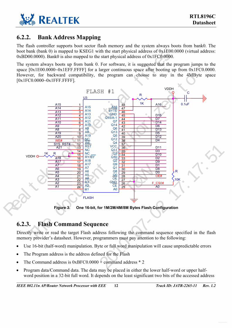
6.2.2. Bank Address Mapping The flash controller supports boot sector flash memory and the system always boots from bank0. The boot bank (bank 0) is mapped to KSEG1 with the start physical address of 0x1E00.0000 (virtual address: 0xBD00.0000). Bank0 is also mapped to the start physical address of 0x1FC0.0000.
The system always boots up from bank 0. For software, it is suggested that the program jumps to the space [0x1E00.0000~0x1EFF.FFFF] for a larger continuous space after booting up from 0x1FC0.0000. However, for backward compatibility, the program can choose to stay in the 4MByte space [0x1FC0.0000~0x1FFF.FFFF].
A4
A12
A18
SYS_RST#
R1K
A10
A16
D10
D15
A5
A3
A1
D11
D12
A7
F_CS0#
C
0.1uF
A19
R
1K
D13
A13
D3
A0
D4
VDDH
OE#
D7
D1
D2
D0
D14
D8
D9
VDDH
A21
A20
D6
A15
A9
A14
D5
R
10K
A11
A8
A2
FLASH #1
A6
WE#
U3
FLASH
123456789
10111213141516171819202122
444342414039383736353433323130292827262524
23
48474645
A15A14A13A12A11A10A9A8A19NCWERSTNCNCRY/BYA18A17A7A6A5A4A3
Q7Q14Q6
Q13Q5
Q12Q4
VCCQ11Q3
Q10Q2Q9Q1Q8Q0OE
GNDCEA0A1
A2
A16BYTEGND
Q15/A-1
A17
Figure 3. One 16-bit, for 1M/2M/4M/8M Bytes Flash Configuration
6.2.3. Flash Command Sequence Directly write or read the target Flash address following the command sequence specified in the flash memory provider’s datasheet. However, programmers must pay attention to the following:
• Use 16-bit (half-word) manipulation. Byte or full word manipulation will cause unpredictable errors
• The Program address is the address defined for the Flash
• The Command address is 0xBFC0.0000 + command address * 2
• Program data/Command data. The data may be placed in either the lower half-word or upper half-word position in a 32-bit full word. It depends on the least significant two bits of the accessed address
www.DataSheet.net/
Datasheet pdf - http://www.DataSheet4U.co.kr/
Realtek confidential files
The document authorized to
T&W
2010-07-02 17:17:51
RTL8196C Datasheet
IEEE 802.11n AP/Router Network Processor with EEE 13 Track ID: JATR-2265-11 Rev. 1.2
6.3. SPI Flash Controller The SPI flash controller is a new design and incorporates new features.
6.3.1. Features • Targeted SPI Flash Frequency: Up to 78MHz (when the SDRAM clock is 156MHz)
• In addition to a programmed I/O interface, also supports a memory-mapped I/O interface for read operations
• Supports Read and Fast Read in memory-mapped I/O mode
6.4. Software Register Definition 6.4.1. Memory Control Register (MCR) (0xB800_1000) This register does not provide byte access.
Table 4. Memory Control Register (MCR) (0xB800_1000) Bit Name Description Mode Default31 DRAMTYPE Report the Hardware Strapping Initial Value for DRAM Type
0: SDR DRAM 1: Reserved R 0B
30 BOOTSEL Report the Hardware Strapping Initial Value for Boot Flash Type 0: NOR flash 1: SPI flash
R 0B
29 IPREF Enable Instruction Prefetch Function 0: Disable prefetch (also resets buffer status) 1: Enable prefetch (4 words)
RW 0B
28 DPREF Enable Data Prefetch Function 0: Disable prefetch (also resets buffer status) 1: Enable prefetch (4 words)
RW 0B
27 IPREF_MODE Choose Instruction Prefetch Mode 0: Old prefetch mechanism 1: New prefetch mechanism
RW 0B
26 DPREF_MODE Choose Data Prefetch Mode 0: Old prefetch mechanism 1: New prefetch mechanism
RW 0B
25 BOOTSEL2 Report the Hardware Strapping Initial Value for Boot Source 0: Flash Type (NOR or SPI Flash) 1: Reserved
R 0B
24:0 Reserved Reserved R 0B
www.DataSheet.net/
Datasheet pdf - http://www.DataSheet4U.co.kr/

Realtek confidential files
The document authorized to
T&W
2010-07-02 17:17:51
RTL8196C Datasheet
IEEE 802.11n AP/Router Network Processor with EEE 14 Track ID: JATR-2265-11 Rev. 1.2
6.4.2. DRAM Configuration Register (DCR) (0xB800_1004) This register does not provide byte access.
Table 5. DRAM Configuration Register (DCR) (0xB800_1004) Bit Name Description Mode Default
31:30 T_CAS CAS Latency 00: Latency=2 01: Latency=3 10: Latency=2.5 11: Reserved
RW 01B
29:28 DBUSWID DRAM Bus Width 00: Reserved 01: 16-bit 10: Reserved 11: Reserved
RW 01B
27 DCHIPSEL DRAM Chip Select 0: Test mode 1: Normal mode
RW 1B
26:25 ROWCNT Row Counts 00: 2K (A0~A10) 01: 4K (A0~A11) 10: 8K (A0~A12) 11: 16K (A0~A13)
RW 00B
24:22 COLCNT Column Counts 000: 256 (A0~A7) 001: 512 (A0~A8) 010: 1K (A0~A9) 011: 2K (A0~A9, A11) 100: 4K (A0~A9, A11, A12) 101: Reserved 110: Reserved 111: Reserved
RW 000B
21 BSTREF Bursted 8 Auto-Refresh Commands (Used for DDR) 0: Disable 1: Enable
RW 0B
20 ARBIT Enforce Interface Arbitration to Take Effect 0: Reserved 1: Take effect
RW 0B
19 BANKCNT Bank Counts 0: 2 banks (used for SDR) 1: 4 banks (used for SDR, DDR)
RW 1B
18 FAST_RX If RX path turnaround delay is small enough, the memory controller can return read data with reduced latency within 1DRAM clock cycle (used for DDR). 0: Normal path 1: Fast path
RW 0B
17 MR_MODE Select the Memory Command that the Memory Controller Issues (Used for DDR) 0: Mode Register 1: Extended Mode Register
RW 0B
16 DRV_STR Drive Strength Setting of DRAM Chip (Used for DDR) For this option to be effective, MR_MODE must be first set to 1. 0: Normal 1: Reduced
RW 0B
15:0 Reserved Reserved - -
www.DataSheet.net/
Datasheet pdf - http://www.DataSheet4U.co.kr/
Realtek confidential files
The document authorized to
T&W
2010-07-02 17:17:51
RTL8196C Datasheet
IEEE 802.11n AP/Router Network Processor with EEE 15 Track ID: JATR-2265-11 Rev. 1.2
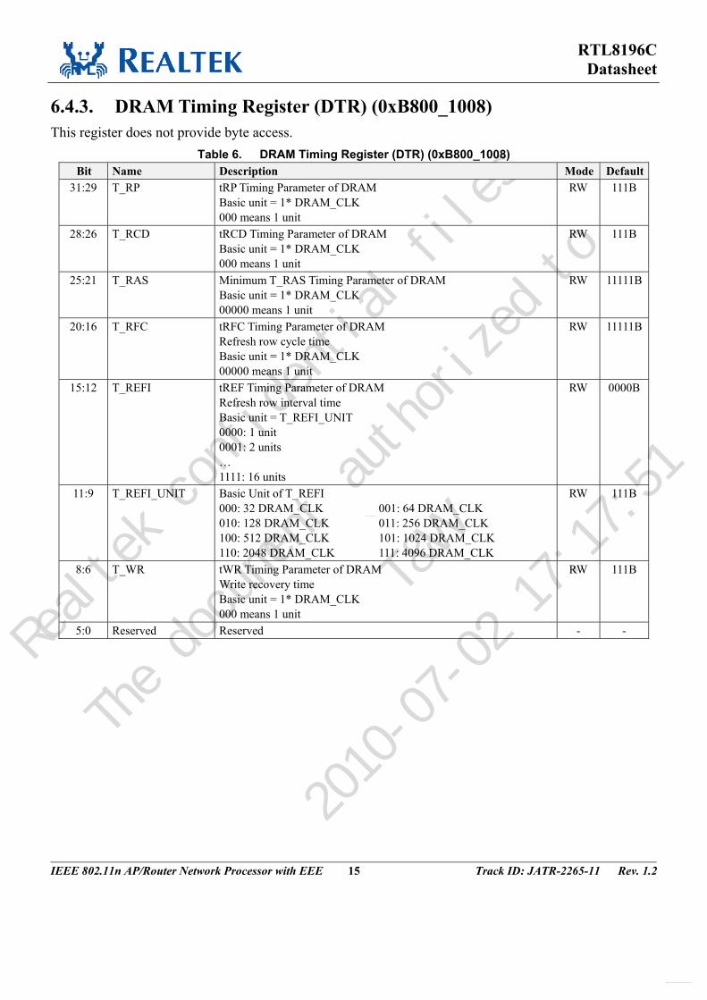
6.4.3. DRAM Timing Register (DTR) (0xB800_1008) This register does not provide byte access.
Table 6. DRAM Timing Register (DTR) (0xB800_1008) Bit Name Description Mode Default
31:29 T_RP tRP Timing Parameter of DRAM Basic unit = 1* DRAM_CLK 000 means 1 unit
RW 111B
28:26 T_RCD tRCD Timing Parameter of DRAM Basic unit = 1* DRAM_CLK 000 means 1 unit
RW 111B
25:21 T_RAS Minimum T_RAS Timing Parameter of DRAM Basic unit = 1* DRAM_CLK 00000 means 1 unit
RW 11111B
20:16 T_RFC tRFC Timing Parameter of DRAM Refresh row cycle time Basic unit = 1* DRAM_CLK 00000 means 1 unit
RW 11111B
15:12 T_REFI tREF Timing Parameter of DRAM Refresh row interval time Basic unit = T_REFI_UNIT 0000: 1 unit 0001: 2 units … 1111: 16 units
RW 0000B
11:9 T_REFI_UNIT Basic Unit of T_REFI 000: 32 DRAM_CLK 001: 64 DRAM_CLK 010: 128 DRAM_CLK 011: 256 DRAM_CLK 100: 512 DRAM_CLK 101: 1024 DRAM_CLK 110: 2048 DRAM_CLK 111: 4096 DRAM_CLK
RW 111B
8:6 T_WR tWR Timing Parameter of DRAM Write recovery time Basic unit = 1* DRAM_CLK 000 means 1 unit
RW 111B
5:0 Reserved Reserved - -
www.DataSheet.net/
Datasheet pdf - http://www.DataSheet4U.co.kr/

Realtek confidential files
The document authorized to
T&W
2010-07-02 17:17:51
RTL8196C Datasheet
IEEE 802.11n AP/Router Network Processor with EEE 16 Track ID: JATR-2265-11 Rev. 1.2
6.4.4. NOR Flash Configuration Register (NFCR) (0xB800_1100) This register does not provide byte access.
Table 7. NOR Flash Configuration Register (NFCR) (0xB800_1100) Bit Name Description Mode Default
31:28 T_CEPL The Timing Interval for CE# to be Pulled-Low before WE#/OE# is Pulled-Low Basic Unit = 1 * DRAM clock cycle 0000 means 1 unit
RW 1111B
27:23 T_WEOEPL The Timing Interval for WE#/OE# to be Pulled-Low Basic Unit = 1 * DRAM clock cycle 00000 means 1 unit
RW 11111B
22:19 T_RDOZ The Timing Interval for OE# to be Pulled-High before Read-Data Output High-Z Basic Unit = 1 * DRAM clock cycle 0000 means 1 unit
RW 1111B
18:16 NFSIZE NOR Flash Size 000: 256Kbyte 001: 512Kbyte 010: 1Mbyte 011: 2Mbyte 100: 4Mbyte 101: 8Mbyte 110: Reserved 111: Reserved
RW 110B
15 NBUSW NOR Flash Bus Width 0: 8-bit 1: 16-bit
R 1B
14:0 Reserved Reserved - -
6.4.5. SPI Flash Configuration Register (SFCR) (0xB800_1200) This register does not provide byte access.
Table 8. SPI Flash Configuration Register (SFCR) (0xB800_1200) Bit Name Description Mode Default
31:29 SPI_CLK_DIV SPI Operating Clock Rate Selection The value defines the divisor to generate the SPI clock. SPI Clock = (SDRAM Clock) / (SPI_CLK_DIV) 000: DIV = 2 001: DIV = 4 010: DIV = 6 011: DIV = 8 100: DIV = 10 101: DIV = 12 110: DIV = 14 111: DIV = 16
RW 111B
28 RBO Serial Flash Read Byte Ordering 0: The byte order is from low to high 1: The byte order is from high to low
RW 1B
27 WBO Serial Flash Write Byte Ordering 0: The byte order is from low to high 1: The byte order is from high to low
RW 1B
26-23 SPI_TCS SPI Chip Deselect Time Basic unit = 1 * DRAM clock cycle 0000 means 1 unit, 0001 means 2 units, etc.
RW 1111B
22:0 Reserved Reserved - -
www.DataSheet.net/
Datasheet pdf - http://www.DataSheet4U.co.kr/
Realtek confidential files
The document authorized to
T&W
2010-07-02 17:17:51
RTL8196C Datasheet
IEEE 802.11n AP/Router Network Processor with EEE 17 Track ID: JATR-2265-11 Rev. 1.2
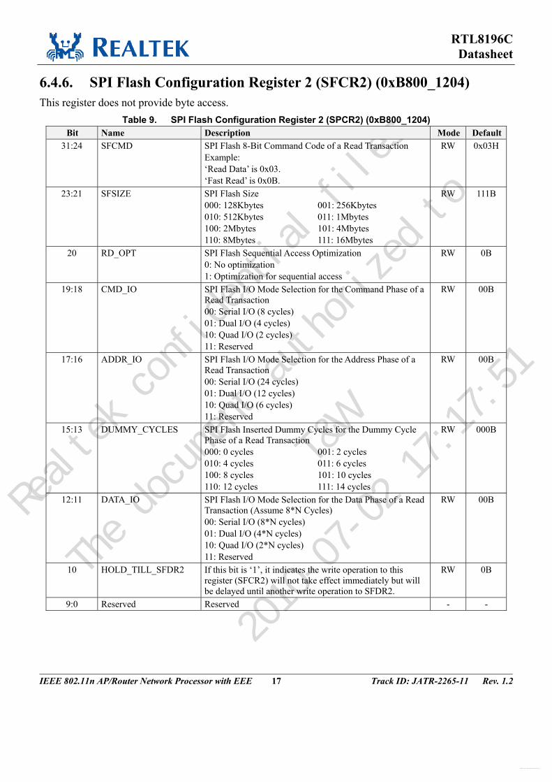
6.4.6. SPI Flash Configuration Register 2 (SFCR2) (0xB800_1204) This register does not provide byte access.
Table 9. SPI Flash Configuration Register 2 (SPCR2) (0xB800_1204) Bit Name Description Mode Default
31:24 SFCMD SPI Flash 8-Bit Command Code of a Read Transaction Example: ‘Read Data’ is 0x03. ‘Fast Read’ is 0x0B.
RW 0x03H
23:21 SFSIZE SPI Flash Size 000: 128Kbytes 001: 256Kbytes 010: 512Kbytes 011: 1Mbytes 100: 2Mbytes 101: 4Mbytes 110: 8Mbytes 111: 16Mbytes
RW 111B
20 RD_OPT SPI Flash Sequential Access Optimization 0: No optimization 1: Optimization for sequential access
RW 0B
19:18 CMD_IO SPI Flash I/O Mode Selection for the Command Phase of a Read Transaction 00: Serial I/O (8 cycles) 01: Dual I/O (4 cycles) 10: Quad I/O (2 cycles) 11: Reserved
RW 00B
17:16 ADDR_IO SPI Flash I/O Mode Selection for the Address Phase of a Read Transaction 00: Serial I/O (24 cycles) 01: Dual I/O (12 cycles) 10: Quad I/O (6 cycles) 11: Reserved
RW 00B
15:13 DUMMY_CYCLES SPI Flash Inserted Dummy Cycles for the Dummy Cycle Phase of a Read Transaction 000: 0 cycles 001: 2 cycles 010: 4 cycles 011: 6 cycles 100: 8 cycles 101: 10 cycles 110: 12 cycles 111: 14 cycles
RW 000B
12:11 DATA_IO SPI Flash I/O Mode Selection for the Data Phase of a Read Transaction (Assume 8*N Cycles) 00: Serial I/O (8*N cycles) 01: Dual I/O (4*N cycles) 10: Quad I/O (2*N cycles) 11: Reserved
RW 00B
10 HOLD_TILL_SFDR2 If this bit is ‘1’, it indicates the write operation to this register (SFCR2) will not take effect immediately but will be delayed until another write operation to SFDR2.
RW 0B
9:0 Reserved Reserved - -
www.DataSheet.net/
Datasheet pdf - http://www.DataSheet4U.co.kr/
Realtek confidential files
The document authorized to
T&W
2010-07-02 17:17:51
RTL8196C Datasheet
IEEE 802.11n AP/Router Network Processor with EEE 18 Track ID: JATR-2265-11 Rev. 1.2
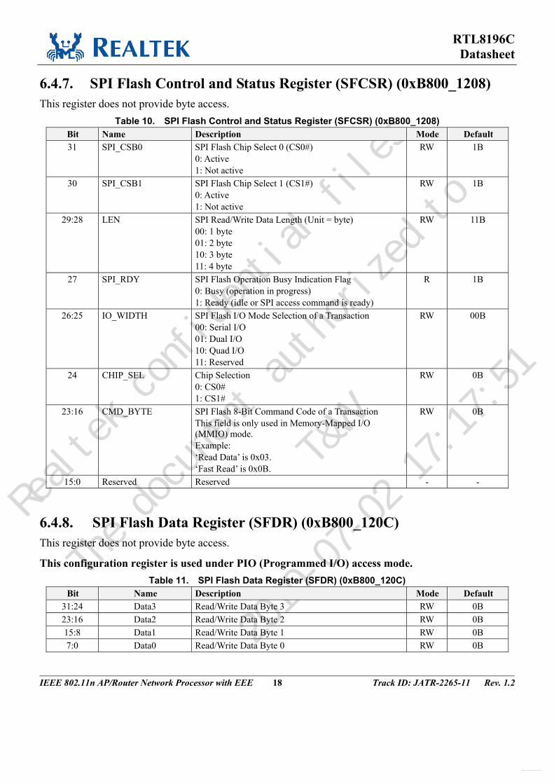
6.4.7. SPI Flash Control and Status Register (SFCSR) (0xB800_1208) This register does not provide byte access.
Table 10. SPI Flash Control and Status Register (SFCSR) (0xB800_1208) Bit Name Description Mode Default 31 SPI_CSB0 SPI Flash Chip Select 0 (CS0#)
0: Active 1: Not active
RW 1B
30 SPI_CSB1 SPI Flash Chip Select 1 (CS1#) 0: Active 1: Not active
RW 1B
29:28 LEN SPI Read/Write Data Length (Unit = byte) 00: 1 byte 01: 2 byte 10: 3 byte 11: 4 byte
RW 11B
27 SPI_RDY SPI Flash Operation Busy Indication Flag 0: Busy (operation in progress) 1: Ready (idle or SPI access command is ready)
R 1B
26:25 IO_WIDTH SPI Flash I/O Mode Selection of a Transaction 00: Serial I/O 01: Dual I/O 10: Quad I/O 11: Reserved
RW 00B
24 CHIP_SEL Chip Selection 0: CS0# 1: CS1#
RW 0B
23:16 CMD_BYTE SPI Flash 8-Bit Command Code of a Transaction This field is only used in Memory-Mapped I/O (MMIO) mode. Example: ‘Read Data’ is 0x03. ‘Fast Read’ is 0x0B.
RW 0B
15:0 Reserved Reserved - -
6.4.8. SPI Flash Data Register (SFDR) (0xB800_120C) This register does not provide byte access.
This configuration register is used under PIO (Programmed I/O) access mode. Table 11. SPI Flash Data Register (SFDR) (0xB800_120C)
Bit Name Description Mode Default 31:24 Data3 Read/Write Data Byte 3 RW 0B 23:16 Data2 Read/Write Data Byte 2 RW 0B 15:8 Data1 Read/Write Data Byte 1 RW 0B 7:0 Data0 Read/Write Data Byte 0 RW 0B
www.DataSheet.net/
Datasheet pdf - http://www.DataSheet4U.co.kr/
Realtek confidential files
The document authorized to
T&W
2010-07-02 17:17:51
RTL8196C Datasheet
IEEE 802.11n AP/Router Network Processor with EEE 19 Track ID: JATR-2265-11 Rev. 1.2
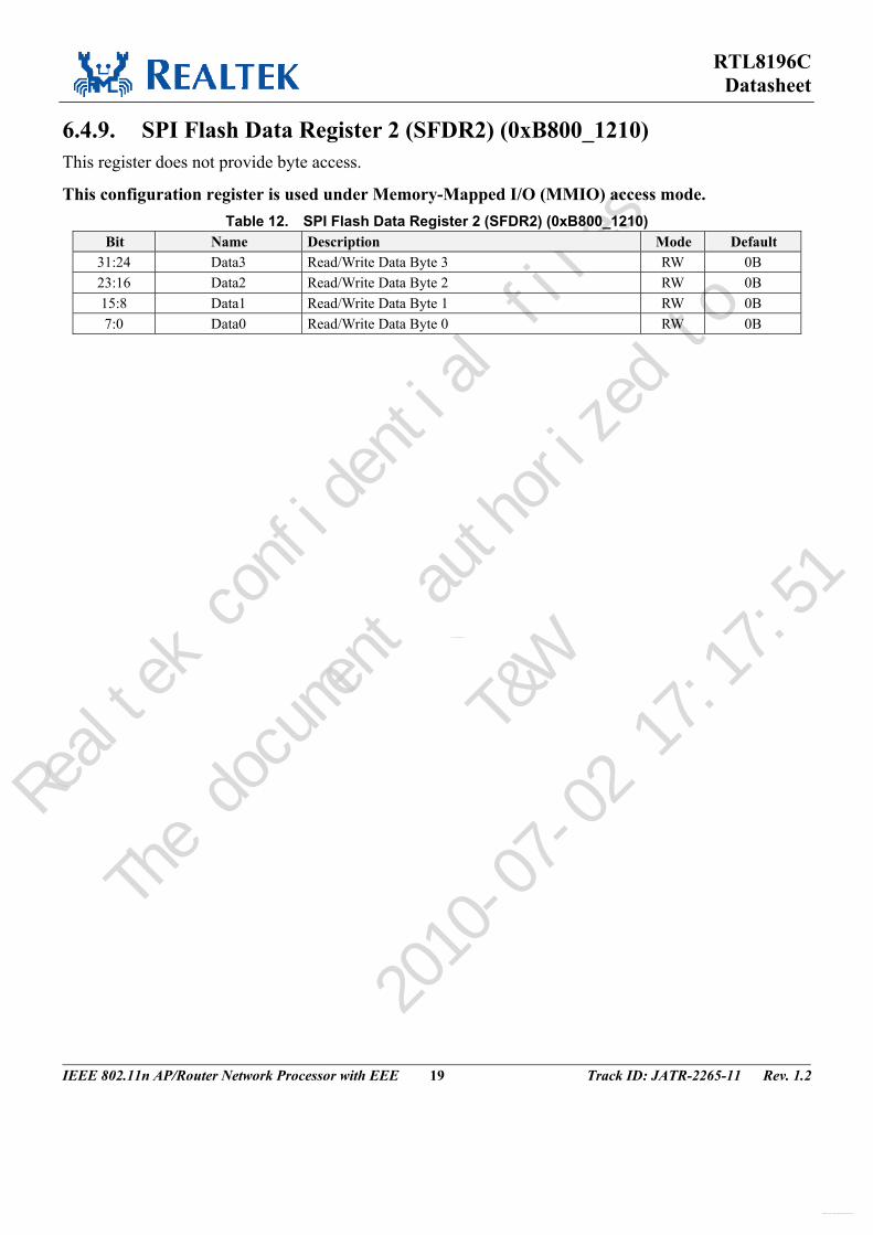
6.4.9. SPI Flash Data Register 2 (SFDR2) (0xB800_1210) This register does not provide byte access.
This configuration register is used under Memory-Mapped I/O (MMIO) access mode. Table 12. SPI Flash Data Register 2 (SFDR2) (0xB800_1210)
Bit Name Description Mode Default 31:24 Data3 Read/Write Data Byte 3 RW 0B 23:16 Data2 Read/Write Data Byte 2 RW 0B 15:8 Data1 Read/Write Data Byte 1 RW 0B 7:0 Data0 Read/Write Data Byte 0 RW 0B
www.DataSheet.net/
Datasheet pdf - http://www.DataSheet4U.co.kr/

Realtek confidential files
The document authorized to
T&W
2010-07-02 17:17:51
RTL8196C Datasheet
IEEE 802.11n AP/Router Network Processor with EEE 20 Track ID: JATR-2265-11 Rev. 1.2
7. Peripheral and MISC Control 7.1. GPIO Control The RTL8196C provides four sets of General Purpose Input/Output (GPIO) pins (GPIO A, B, C, D). Each GPIO pin may be configured as an input or output pin. The GPIO DATA register may be used to control GPIO pin signals. The GPIO pins are shared with some peripheral pins, and the type of peripheral can affect the attributes of the shared pins. All GPIO sets can be used to generate interrupts, and an interrupt mask and status register are provided. All the GPIO control registers are defined in the following tables.
7.1.1. GPIO Register Set (0xB800_3500) Table 13. GPIO Register Set (0xB800_3500)
Offset Size (byte) Name Description 0x00 4 PABCD_CNR Port A, B, C, D Control Register 0x08 4 PABCD_DIR Port A, B, C, D Direction Register 0x0C 4 PABCD_DAT Port A, B, C, D Data Register 0x10 4 PABCD_ISR Port A, B, C, D Interrupt Status Register 0x14 4 PAB_IMR Port A, B Interrupt Mask Register 0x18 4 PCD_IMR Port C, D Interrupt Mask Register
7.1.2. GPIO Port A, B, C, D Control Register (PABCD_CNR) (0xB800_3500)
Table 14. GPIO Port A, B, C, D Control Register (PABCD_CNR) (0xB800_3500) Bit Name Description RW Default
31:24 PFC_D[7:0] Pin Function Configuration of Port D RW FFH 23:16 PFC_C[7:0] Pin Function Configuration of Port C RW FFH 15:8 PFC_B[7:0] Pin Function Configuration of Port B RW FFH 7:0 PFC_A[7:0] Pin Function Configuration of Port A
Bit Value: 0: Configured as GPIO pin 1: Configured as dedicated peripheral pin
RW FFH
www.DataSheet.net/
Datasheet pdf - http://www.DataSheet4U.co.kr/

Realtek confidential files
The document authorized to
T&W
2010-07-02 17:17:51
RTL8196C Datasheet
IEEE 802.11n AP/Router Network Processor with EEE 21 Track ID: JATR-2265-11 Rev. 1.2
7.1.3. GPIO Port A, B, C, D Direction Register (PABCD_DIR) (0xB800_3508)
Table 15. GPIO Port A, B, C, D Direction Register (PABCD_DIR) (0xB800_3508) Bit Name Description RW Default
31:24 DRC_D[7:0] Pin Direction Configuration of Port D 0: Configured as input pin 1: Configured as output pin
RW 00H
23:16 DRC_C[7:0] Pin Direction Configuration of Port C 0: Configured as input pin 1: Configured as output pin
RW 00H
15:8 DRC_B[7:0] Pin Direction Configuration of Port B 0: Configured as input pin 1: Configured as output pin
RW 00H
7:0 DRC_A[7:0] Pin Direction Configuration of Port A 0: Configured as input pin 1: Configured as output pin
RW 00H
7.1.4. Port A, B, C, D Data Register (PABCD_DAT) (0xB800_350C) Table 16. Port A, B, C, D Data Register (PABCD_DAT) (0xB800_350C)
Bit Name Description RW Default 31:24 PD_D[7:0] Pin Data of Port D
0: Data=0 1: Data=1 RW 00H
23:16 PD_C[7:0] Pin Data of Port C 0: Data=0 1: Data=1
RW 00H
15:8 PD_B[7:0] Pin Data of Port B 0: Data=0 1: Data=1
RW 00H
7:0 PD_A[7:0] Pin Data of Port A 0: Data=0 1: Data=1
RW 00H
7.1.5. Port A, B, C, D Interrupt Status Register (PABCD_ISR) (0xB800_3510)
Table 17. Port A, B, C, D Interrupt Status Register (PABCD_ISR) (0xB800_3510) Bit Name Description RW Default
31:24 IPS_D[7:0] Interrupt Pending Status of Port D Write ‘1’ to clear the interrupt
RW 00H
23:16 IPS_C[7:0] Interrupt Pending Status of Port C Write ‘1’ to clear the interrupt
RW 00H
15:8 IPS_B[7:0] Interrupt Pending Status of Port B Write ‘1’ to clear the interrupt
RW 00H
7:0 IPS_A[7:0] Interrupt Pending Status of Port A Write ‘1’ to clear the interrupt
RW 00H
www.DataSheet.net/
Datasheet pdf - http://www.DataSheet4U.co.kr/

Realtek confidential files
The document authorized to
T&W
2010-07-02 17:17:51
RTL8196C Datasheet
IEEE 802.11n AP/Router Network Processor with EEE 22 Track ID: JATR-2265-11 Rev. 1.2
7.1.6. Port A, B Interrupt Mask Register (PAB_IMR) (0xB800_3514) Table 18. Port A, B Interrupt Mask Register (PAB_IMR) (0xB800_3514)
Bit Name Description RW Default 31:30 PB7_IM[1:0] PortB.7 Interrupt Mode RW 00B 29:28 PB6_IM[1:0] PortB.6 Interrupt Mode RW 00B 27:26 PB5_IM[1:0] PortB.5 Interrupt Mode RW 00B 25:24 PB4_IM[1:0] PortB.4 Interrupt Mode RW 00B 23:22 PB3_IM[1:0] PortB.3 Interrupt Mode RW 00B 21:20 PB2_IM[1:0] PortB.2 Interrupt Mode RW 00B 19:18 PB1_IM[1:0] PortB.1 Interrupt Mode RW 00B 17:16 PB0_IM[1:0] PortB.0 Interrupt Mode RW 00B 15:14 PA7_IM[1:0] PortA.7 Interrupt Mode RW 00B 13:12 PA6_IM[1:0] PortA.6 Interrupt Mode RW 00B 11:10 PA5_IM[1:0] PortA.5 Interrupt Mode RW 00B 9:8 PA4_IM[1:0] PortA.4 Interrupt Mode RW 00B 7:6 PA3_IM[1:0] PortA.3 Interrupt Mode RW 00B 5:4 PA2_IM[1:0] PortA.2 Interrupt Mode RW 00B 3:2 PA1_IM[1:0] PortA.1 Interrupt Mode RW 00B 1:0 PA0_IM[1:0] PortA.0 Interrupt Mode
00: Disable interrupt 01: Enable falling edge interrupt 10: Enable rising edge interrupt 11: Enable both falling or rising edge interrupt
RW 00B
7.1.7. Port C, D Interrupt Mask Register (PCD_IMR) (0xB800_3518) Table 19. Port C, D Interrupt Mask Register (PCD_IMR) (0xB800_3518)
Bit Name Description RW Default 31:30 PD7_IM[1:0] PortD.7 Interrupt Mode RW 00B 29:28 PD6_IM[1:0] PortD.6 Interrupt Mode RW 00B 27:26 PD5_IM[1:0] PortD.5 Interrupt Mode RW 00B 25:24 PD4_IM[1:0] PortD.4 Interrupt Mode RW 00B 23:22 PD3_IM[1:0] PortD.3 Interrupt Mode RW 00B 21:20 PD2_IM[1:0] PortD.2 Interrupt Mode RW 00B 19:18 PD1_IM[1:0] PortD.1 Interrupt Mode RW 00B 17:16 PD0_IM[1:0] PortC.0 Interrupt Mode RW 00B 15:14 PC7_IM[1:0] PortC.7 Interrupt Mode RW 00B 13:12 PC6_IM[1:0] PortC.6 Interrupt Mode RW 00B 11:10 PC5_IM[1:0] PortC.5 Interrupt Mode RW 00B 9:8 PC4_IM[1:0] PortC.4 Interrupt Mode RW 00B 7:6 PC3_IM[1:0] PortC.3 Interrupt Mode RW 00B 5:4 PC2_IM[1:0] PortC.2 Interrupt Mode RW 00B 3:2 PC1_IM[1:0] PortC.1 Interrupt Mode RW 00B 1:0 PC0_IM[1:0] PortC.0 Interrupt Mode
00: Disable interrupt 01: Enable falling edge interrupt 10: Enable rising edge interrupt 11: Enable both falling or rising edge interrupt
RW 00B
www.DataSheet.net/
Datasheet pdf - http://www.DataSheet4U.co.kr/
Realtek confidential files
The document authorized to
T&W
2010-07-02 17:17:51
RTL8196C Datasheet
IEEE 802.11n AP/Router Network Processor with EEE 23 Track ID: JATR-2265-11 Rev. 1.2
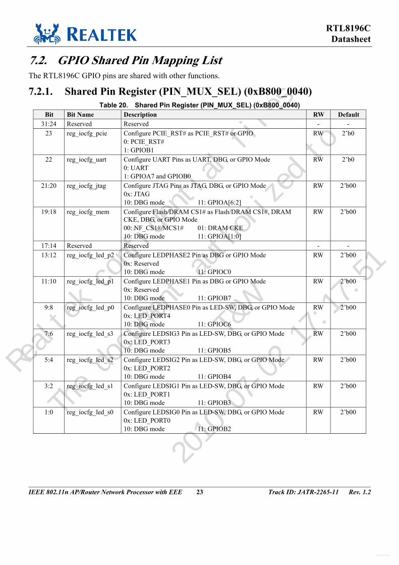
7.2. GPIO Shared Pin Mapping List The RTL8196C GPIO pins are shared with other functions.
7.2.1. Shared Pin Register (PIN_MUX_SEL) (0xB800_0040) Table 20. Shared Pin Register (PIN_MUX_SEL) (0xB800_0040)
Bit Bit Name Description RW Default 31:24 Reserved Reserved - -
23 reg_iocfg_pcie Configure PCIE_RST# as PCIE_RST# or GPIO 0: PCIE_RST# 1: GPIOB1
RW 2’b0
22 reg_iocfg_uart Configure UART Pins as UART, DBG, or GPIO Mode 0: UART 1: GPIOA7 and GPIOB0
RW 2’b0
21:20 reg_iocfg_jtag Configure JTAG Pins as JTAG, DBG, or GPIO Mode 0x: JTAG 10: DBG mode 11: GPIOA[6:2]
RW 2’b00
19:18 reg_iocfg_mem Configure Flash/DRAM CS1# as Flash/DRAM CS1#, DRAM CKE, DBG, or GPIO Mode 00: NF_CS1#/MCS1# 01: DRAM CKE 10: DBG mode 11: GPIOA[1:0]
RW 2’b00
17:14 Reserved Reserved - - 13:12 reg_iocfg_led_p2 Configure LEDPHASE2 Pin as DBG or GPIO Mode
0x: Reserved 10: DBG mode 11: GPIOC0
RW 2’b00
11:10 reg_iocfg_led_p1 Configure LEDPHASE1 Pin as DBG or GPIO Mode 0x: Reserved 10: DBG mode 11: GPIOB7
RW 2’b00
9:8 reg_iocfg_led_p0 Configure LEDPHASE0 Pin as LED-SW, DBG, or GPIO Mode 0x: LED_PORT4 10: DBG mode 11: GPIOC6
RW 2’b00
7:6 reg_iocfg_led_s3 Configure LEDSIG3 Pin as LED-SW, DBG, or GPIO Mode 0x: LED_PORT3 10: DBG mode 11: GPIOB5
RW 2’b00
5:4 reg_iocfg_led_s2 Configure LEDSIG2 Pin as LED-SW, DBG, or GPIO Mode 0x: LED_PORT2 10: DBG mode 11: GPIOB4
RW 2’b00
3:2 reg_iocfg_led_s1 Configure LEDSIG1 Pin as LED-SW, DBG, or GPIO Mode 0x: LED_PORT1 10: DBG mode 11: GPIOB3
RW 2’b00
1:0 reg_iocfg_led_s0 Configure LEDSIG0 Pin as LED-SW, DBG, or GPIO Mode 0x: LED_PORT0 10: DBG mode 11: GPIOB2
RW 2’b00
www.DataSheet.net/
Datasheet pdf - http://www.DataSheet4U.co.kr/
Realtek confidential files
The document authorized to
T&W
2010-07-02 17:17:51
RTL8196C Datasheet
IEEE 802.11n AP/Router Network Processor with EEE 24 Track ID: JATR-2265-11 Rev. 1.2
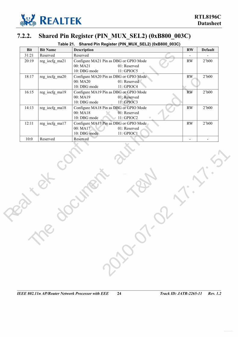
7.2.2. Shared Pin Register (PIN_MUX_SEL2) (0xB800_003C) Table 21. Shared Pin Register (PIN_MUX_SEL2) (0xB800_003C)
Bit Bit Name Description RW Default 31:21 Reserved Reserved - - 20:19 reg_iocfg_ma21 Configure MA21 Pin as DBG or GPIO Mode
00: MA21 01: Reserved 10: DBG mode 11: GPIOC5
RW 2’b00
18:17 reg_iocfg_ma20 Configure MA20 Pin as DBG or GPIO Mode 00: MA20 01: Reserved 10: DBG mode 11: GPIOC4
RW 2’b00
16:15 reg_iocfg_ma19 Configure MA19 Pin as DBG or GPIO Mode 00: MA19 01: Reserved 10: DBG mode 11: GPIOC3
RW 2’b00
14:13 reg_iocfg_ma18 Configure MA18 Pin as DBG or GPIO Mode 00: MA18 01: Reserved 10: DBG mode 11: GPIOC2
RW 2’b00
12:11 reg_iocfg_ma17 Configure MA17 Pin as DBG or GPIO Mode 00: MA17 01: Reserved 10: DBG mode 11: GPIOC1
RW 2’b00
10:0 Reserved Reserved - -
www.DataSheet.net/
Datasheet pdf - http://www.DataSheet4U.co.kr/

Realtek confidential files
The document authorized to
T&W
2010-07-02 17:17:51
RTL8196C Datasheet
IEEE 802.11n AP/Router Network Processor with EEE 25 Track ID: JATR-2265-11 Rev. 1.2
8. Green Ethernet 8.1. Cable Length Power Saving The RTL8196C provides link-on and dynamic detection of cable length, and dynamic adjustment of power required for the detected cable length. This feature provides high performance with minimum power consumption.
8.2. Link Down Power Saving The RTL8196C implements link-down power saving on a per-port basis, greatly cutting power consumption when the network cable is disconnected. A port automatically enters link down power saving mode ten seconds after the cable is disconnected from it. Once a port enters link down power saving mode, it transmits normal link pulses on its TXOP/TXON pins and continues to monitor the RXIP/RXIN pins to detect incoming signals, which might be 100Base-TX MLT-3 idle pattern, 10Base-T link pulses, or Auto-Negotiation’s FLP (Fast Link Pulse). After it detects an incoming signal, it wakes up from link down power saving mode and operates in normal mode according to the result of the connection.
8.3. Energy Efficient Ethernet (EEE) The RTL8196C supports IEEE 802.3az Draft 2.0, also known as Energy Efficient Ethernet (EEE) in 100Base-TX in full duplex operation, and 10Base-T in full/half duplex mode. This standard is being developed by the IEEE 802.3az Task Force, and should be finalized by September 2010. It provides a protocol to coordinate transitions to/from a lower power consumption level (Low Power Idle mode) based on link utilization. When no packets are being transmitted, the system goes to Low Power Idle mode to save power. Once packets need to be transmitted, the system returns to normal mode, and does this without changing the link status and without dropping/corrupting frames.
To save power, when the system is in Low Power Idle mode, most of the circuits are disabled, however, the transition time to/from Low Power Idle mode is kept small enough to be transparent to upper layer protocols and applications.
EEE also specifies a negotiation method to enable link partners to determine whether EEE is supported and to select the best set of parameters common to both devices.
• For 100Base-TX PHY: Supports Energy Efficient Ethernet with the optional function of Low Power Idle.
• For 10Base-T, EEE defines a 10Mbps PHY (10Base-Te) with reduced transmit amplitude requirements. 10Base-Te is fully interoperable with 10Base-T PHYs over 100m of class-D (Cat-5) cable.
Refer to http://ieee802.org/3/interims/index.html for more details.
www.DataSheet.net/
Datasheet pdf - http://www.DataSheet4U.co.kr/

Realtek confidential files
The document authorized to
T&W
2010-07-02 17:17:51
RTL8196C Datasheet
IEEE 802.11n AP/Router Network Processor with EEE 26 Track ID: JATR-2265-11 Rev. 1.2
9. DC Specifications 9.1. Operating Conditions
Table 22. Operating Conditions Symbol Parameter Min. Typ. Max. Units VDD33 Digital I/O Power Supply 3.3V 3.135 3.3 3.465 V AVDD33 Ethernet Analog Power Supply 3.3V 3.135 3.3 3.465 V VDD10 Core Power Supply 1.0V 0.95 1.0 1.05 V AVDD10 Ethernet Analog Power Supply 1.0V 0.95 1.0 1.05 V AVDD33_X25M 25M Crystal Power 3.3V 3.135 3.3 3.465 V VDD33_BG System Bandgap Power Supply 3.3V 3.135 3.3 3.465 V AVDD10_PCIE PCI Express Analog Power 1.0V 0.95 1.0 1.05 V AVDD10_PHYPLL Ethernet PHY PLL Power 1.0V 0.95 1.0 1.05 V AVDD33_USB_PCIE USB 2.0 Analog Power 3.3V 3.135 3.3 3.465 V VDD10_USB USB 2.0 Analog Power 1.0V 0.95 1.0 1.05 V
9.2. Power Dissipation Table 23. Power Dissipation
Parameter SYM Conditions Typ. Units Power Supply Current for VDD33 IVDD33 All LAN Ports Idle
LAN Full Load Active for Link at 10Base-T LAN Full Load Active for Link at 100Base-TX
8 25 25
mA
Power Supply Current for VDD10 IVDD10 All LAN Ports Idle and CPU Suspend All LAN Ports Idle LAN Full Load Active for Link at 10Base-T LAN Full Load Active for Link at 100Base-TX
110 210 300 300
mA
3.3V Ethernet Analog Current for AVDD33
IAVDD33 All LAN Ports Idle LAN Ports no Load Link at 10Base-T LAN Ports no Load Link at 10Base-T (EEE) LAN Ports no Load Link at 100Base-T LAN Ports no Load Link at 100Base-T (EEE) LAN Full Load Active for Link at 10Base-T LAN Full Load Active for Link at 100Base-TX
30 72 72 72 13 113 72
mA
1.0V Ethernet Analog Current for AVDD10
IAVDD10 All LAN Ports Idle LAN Ports no Load Link at 10Base-T LAN Ports no Load Link at 10Base-T (EEE) LAN Ports no Load Link at 100Base-T LAN Ports no Load Link at 100Base-T (EEE) LAN Full Load Active for Link at 10Base-T LAN Full Load Active for Link at 100Base-TX
5 5 5
48 5 5
48
mA
3.3V Current for AVDD33_X25M IAVDDX 25M Crystal 3.3V Current 2 mA 3.3V Current for AVDD33_BG IAVDDBG System Bandgap 3.3V Current 18 mA 1.0V Current for AVDD10_PCIE IPCIE PCI Express 1.0V Current 63 mA 1.0V Current for AVDD10_PHYPLL
IPHYPLL Ethernet PHY PLL Power 1.0V 4 mA
www.DataSheet.net/
Datasheet pdf - http://www.DataSheet4U.co.kr/
Realtek confidential files
The document authorized to
T&W
2010-07-02 17:17:51
RTL8196C Datasheet
IEEE 802.11n AP/Router Network Processor with EEE 27 Track ID: JATR-2265-11 Rev. 1.2
Parameter SYM Conditions Typ. Units 3.3V Current for AVDD33_USB_PCIE
IUSB_AVDD33 USB 2.0 and PCI Express Analog Power 3.3V 13 mA
1.0V Current for VDD10_USB ILV_USB_PCIE USB 2.0 Analog Power 1.0V 21 mA Total Power Consumption PS All LAN Ports Idle and CPU Suspended
All LAN Ports Idle LAN Full Load Active for Link at 10Base-T LAN Full Load Active for Link at 100Base-TX
0.34 0.51 0.92 0.83
Watt
9.3. SDRAM Bus DC Parameters Table 24. SDRAM Bus DC Parameters
Symbol Parameter Conditions Min. Typ. Max. Units Notes VIH Input-High Voltage LVTTL 2.0 - - V 1 VIL Input-Low Voltage LVTTL - - 0.8 V 2 VOH Output-High Voltage - 2.4 - - V 3 VOL Output-Low Voltage - - - 0.4 V 3 IIL Input-Leakage Current VIN=3.3V or 0 -10 ±1 10 µA - IOZ Tri-State Output-Leakage Current - -10 ±1 10 µA - RPU Input Pull-Up Resistance - - 75 - KΩ 4 RPD Input Pull-Down Resistance - - 75 - KΩ 4
Note 1: VIH overshot: VIH (MAX)=VDDH + 2V for a pulse width ≤ 3ns, and the pulse width not greater than one third of the cycle rate. Note 2: VIL undershot: VIL (MIN)=-2V for a pulse width ≤ 3ns cannot be exceeded. Note 3: The output current buffer is 16mA for SDRAM clock, address, and data bus. Note 4: These values are typical values checked in the manufacturing process and are not tested.
9.4. Flash Bus DC Parameters Table 25. Flash Bus DC Parameters
Symbol Parameter Conditions Min. Typ. Max. Units Notes VIH Input-High Voltage LVTTL 2.0 - - V 1 VIL Input-Low Voltage LVTTL - - 0.8 V 2 VOH Output-High Voltage - 2.4 - - V 3 VOL Output-Low Voltage - - - 0.4 V 3 IIL Input-Leakage Current VIN=3.3V or 0 -10 ±1 10 µA - IOZ Tri-State Output-Leakage Current - -10 ±1 10 µA - RPU Input Pull-Up Resistance - - 75 - KΩ 4 RPD Input Pull-Down Resistance - - 75 - KΩ 4
Note 1: VIH overshot: VIH (MAX)=VDDH + 2V for a pulse width ≤ 3ns. Note 2: VIL undershot: VIL (MIN)= -2V for a pulse width ≤ 3ns. Note 3: The output current buffer is 8mA for the flash address and data bus; and is 8mA for Flash control signals. Note 4: These values are typical values checked in the manufacturing process and are not tested.
www.DataSheet.net/
Datasheet pdf - http://www.DataSheet4U.co.kr/
Realtek confidential files
The document authorized to
T&W
2010-07-02 17:17:51
RTL8196C Datasheet
IEEE 802.11n AP/Router Network Processor with EEE 28 Track ID: JATR-2265-11 Rev. 1.2
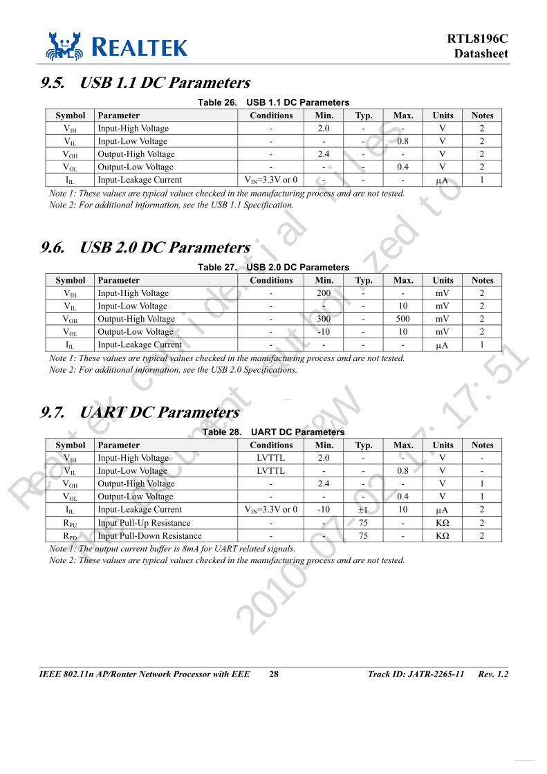
9.5. USB 1.1 DC Parameters Table 26. USB 1.1 DC Parameters
Symbol Parameter Conditions Min. Typ. Max. Units Notes VIH Input-High Voltage - 2.0 - - V 2 VIL Input-Low Voltage - - - 0.8 V 2 VOH Output-High Voltage - 2.4 - - V 2 VOL Output-Low Voltage - - - 0.4 V 2 IIL Input-Leakage Current VIN=3.3V or 0 - - - µA 1
Note 1: These values are typical values checked in the manufacturing process and are not tested. Note 2: For additional information, see the USB 1.1 Specification.
9.6. USB 2.0 DC Parameters Table 27. USB 2.0 DC Parameters
Symbol Parameter Conditions Min. Typ. Max. Units Notes VIH Input-High Voltage - 200 - - mV 2 VIL Input-Low Voltage - - - 10 mV 2 VOH Output-High Voltage - 300 - 500 mV 2 VOL Output-Low Voltage - -10 - 10 mV 2 IIL Input-Leakage Current - - - - µA 1
Note 1: These values are typical values checked in the manufacturing process and are not tested. Note 2: For additional information, see the USB 2.0 Specifications.
9.7. UART DC Parameters Table 28. UART DC Parameters
Symbol Parameter Conditions Min. Typ. Max. Units Notes VIH Input-High Voltage LVTTL 2.0 - - V - VIL Input-Low Voltage LVTTL - - 0.8 V - VOH Output-High Voltage - 2.4 - - V 1 VOL Output-Low Voltage - - - 0.4 V 1 IIL Input-Leakage Current VIN=3.3V or 0 -10 ±1 10 µA 2
RPU Input Pull-Up Resistance - - 75 - KΩ 2 RPD Input Pull-Down Resistance - - 75 - KΩ 2
Note 1: The output current buffer is 8mA for UART related signals. Note 2: These values are typical values checked in the manufacturing process and are not tested.
www.DataSheet.net/
Datasheet pdf - http://www.DataSheet4U.co.kr/

Realtek confidential files
The document authorized to
T&W
2010-07-02 17:17:51
RTL8196C Datasheet
IEEE 802.11n AP/Router Network Processor with EEE 29 Track ID: JATR-2265-11 Rev. 1.2
9.8. GPIO DC Parameters Table 29. GPIO DC Parameters
Symbol Parameter Conditions Min. Typ. Max. Units Notes VIH Input-High Voltage LVTTL 2.0 - - V - VIL Input-Low Voltage LVTTL - - 0.8 V - VOH Output-High Voltage - 2.4 - - V 1 VOL Output-Low Voltage - - - 0.4 V 1 IIL Input-Leakage Current - -10 ±1 10 µA 2
RPD Input Pull-Down Resistance - - 75 - KΩ 2 Note 1: The output current buffer is 8mA for GPIO related signals. Note 2: These values are typical values checked in the manufacturing process and are not tested.
9.9. JTAG DC Parameters Table 30. JTAG DC Parameters
Symbol Parameter Conditions Min. Typ. Max. Units Notes VIH Input-High Voltage LVTTL 2.0 - - V - VIL Input-Low Voltage LVTTL - - 0.8 V - VOH Output-High Voltage ⎢IOH⎢=2~16mA 2.4 - - V 1 VOL Output-Low Voltage ⎢IOL⎢=2~16mA - - 0.4 V 1 IIL Input-Leakage Current - -10 ±1 10 µA 2
RPD Input Pull-Down Resistance - - 75 - KΩ 2 Note 1: The output current buffer is 8mA for JTAG related signals. Note 2: These values are typical values checked in the manufacturing process and are not tested.
9.10. LED DC Parameters Table 31. LED DC Parameters
Symbol Parameter Conditions Min. Typ. Max. Units VOHED Output-High Voltage - 2.4 - - V VOLLED Output-Low Voltage - - - 0.4 V
Note: The output current buffer for LED signals is 8mA.
www.DataSheet.net/
Datasheet pdf - http://www.DataSheet4U.co.kr/

Realtek confidential files
The document authorized to
T&W
2010-07-02 17:17:51
RTL8196C Datasheet
IEEE 802.11n AP/Router Network Processor with EEE 30 Track ID: JATR-2265-11 Rev. 1.2
10. AC Specifications 10.1. Clock Signal Timing
Table 32. Clock Signal Timing Symbol Parameter Min. Typ. Max. Units Notes
VIH Input-High Voltage 2.0 - - V - VIL Input-Low Voltage - - 0.8 V -
TFREQUENCY Clock Frequency for RTL8196C Crystal or Oscillator - 25 - MHz 1 ∆FREQUENCY Clock Tolerance (between 0ºC~50ºC) -50 - 50 ppm -
CSHUNT Crystal Parameter Note: Sometimes referred to as the Holder Capacitance.
- - 7 pF 2
C1 Load Capacitance - - 30 pF 3 C2 Load Capacitance - - 30 pF 3
TDC Duty Cycle Note: This parameter applies when driving the clock input with an oscillator.
- 50 - % -
Note 1: This value could be an oscillator input or a series resonant frequency from a crystal. If used as an oscillator input, tie to the crystal input pin and leave the crystal output pin disconnected. Note 2: The 25MHz Crystal CL=16pF is used on the RTL8196C. Note 3: The RTL8196C PLL circuit requires an external 25MHz crystal with shunt capacitors. These shunt capacitors cannot be over 30pF due to chip design requirements.
Figure 4. Typical Connection to a Crystal
Figure 5. Typical Connection to an Oscillator
www.DataSheet.net/
Datasheet pdf - http://www.DataSheet4U.co.kr/
Realtek confidential files
The document authorized to
T&W
2010-07-02 17:17:51
RTL8196C Datasheet
IEEE 802.11n AP/Router Network Processor with EEE 31 Track ID: JATR-2265-11 Rev. 1.2
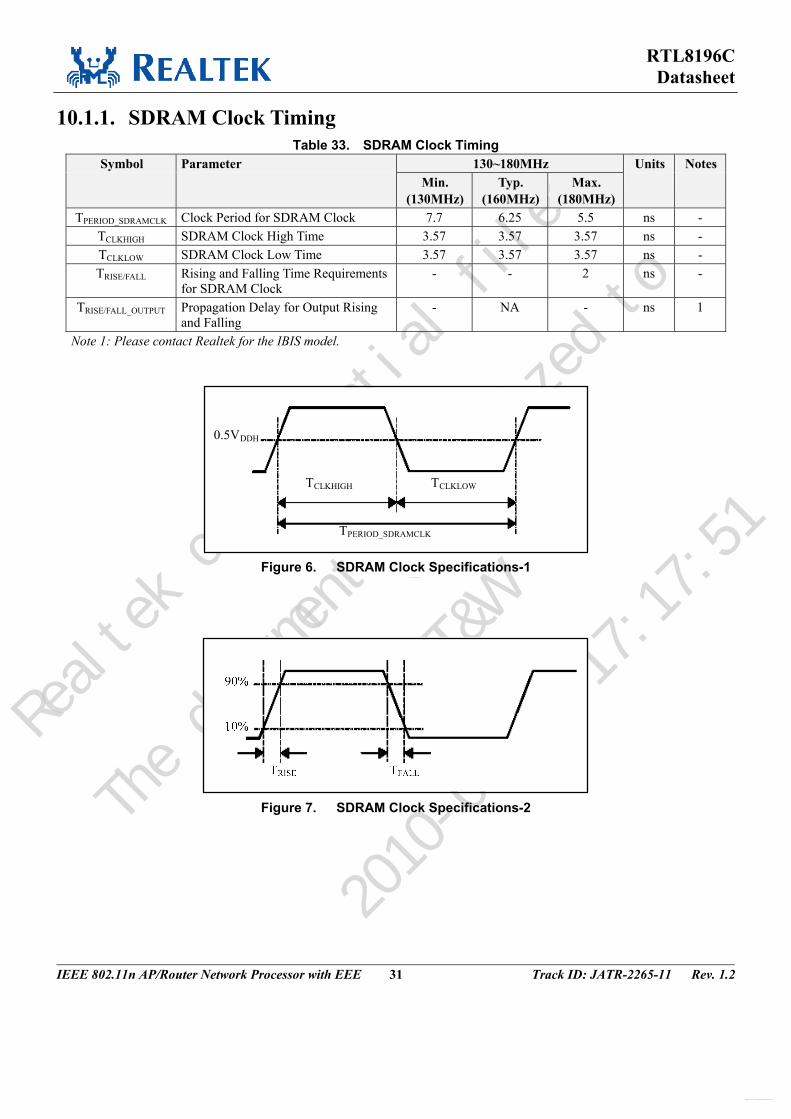
10.1.1. SDRAM Clock Timing Table 33. SDRAM Clock Timing
Symbol Parameter 130~180MHz Units Notes Min.
(130MHz) Typ.
(160MHz) Max.
(180MHz)
TPERIOD_SDRAMCLK Clock Period for SDRAM Clock 7.7 6.25 5.5 ns - TCLKHIGH SDRAM Clock High Time 3.57 3.57 3.57 ns - TCLKLOW SDRAM Clock Low Time 3.57 3.57 3.57 ns - TRISE/FALL Rising and Falling Time Requirements
for SDRAM Clock - - 2 ns -
TRISE/FALL_OUTPUT Propagation Delay for Output Rising and Falling
- NA - ns 1
Note 1: Please contact Realtek for the IBIS model.
TPERIOD_SDRAMCLK
TCLKHIGH TCLKLOW
0.5VDDH
Figure 6. SDRAM Clock Specifications-1
Figure 7. SDRAM Clock Specifications-2
www.DataSheet.net/
Datasheet pdf - http://www.DataSheet4U.co.kr/
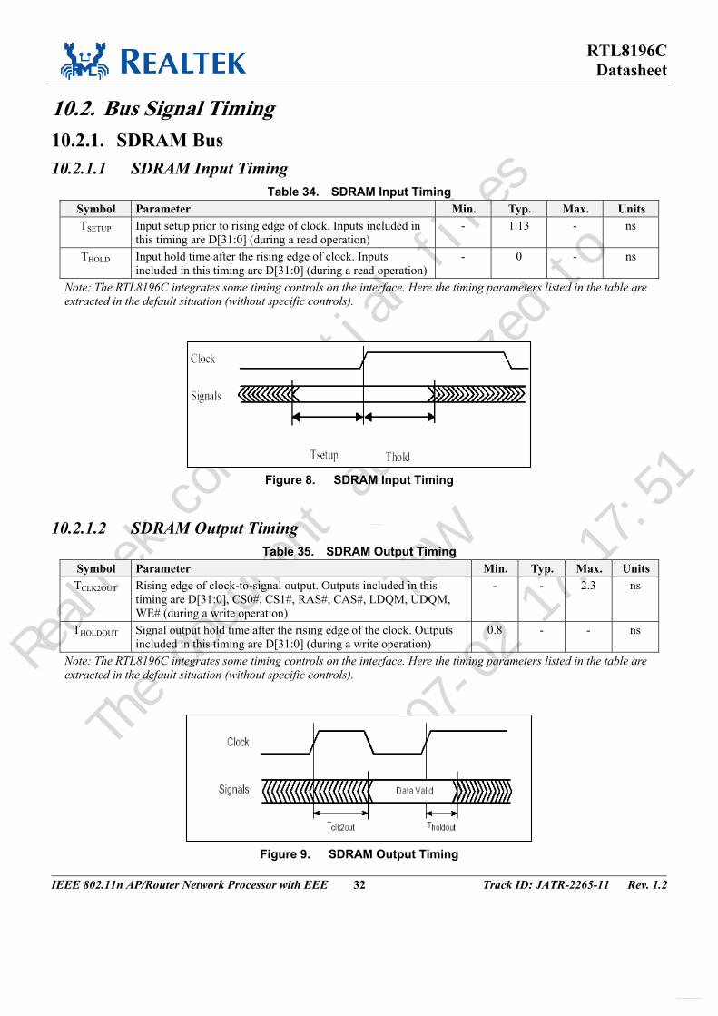
Realtek confidential files
The document authorized to
T&W
2010-07-02 17:17:51
RTL8196C Datasheet
IEEE 802.11n AP/Router Network Processor with EEE 32 Track ID: JATR-2265-11 Rev. 1.2
10.2. Bus Signal Timing 10.2.1. SDRAM Bus 10.2.1.1 SDRAM Input Timing
Table 34. SDRAM Input Timing Symbol Parameter Min. Typ. Max. Units TSETUP Input setup prior to rising edge of clock. Inputs included in
this timing are D[31:0] (during a read operation) - 1.13 - ns
THOLD Input hold time after the rising edge of clock. Inputs included in this timing are D[31:0] (during a read operation)
- 0 - ns
Note: The RTL8196C integrates some timing controls on the interface. Here the timing parameters listed in the table are extracted in the default situation (without specific controls).
Figure 8. SDRAM Input Timing
10.2.1.2 SDRAM Output Timing Table 35. SDRAM Output Timing
Symbol Parameter Min. Typ. Max. Units TCLK2OUT Rising edge of clock-to-signal output. Outputs included in this
timing are D[31:0], CS0#, CS1#, RAS#, CAS#, LDQM, UDQM, WE# (during a write operation)
- - 2.3 ns
THOLDOUT Signal output hold time after the rising edge of the clock. Outputs included in this timing are D[31:0] (during a write operation)
0.8 - - ns
Note: The RTL8196C integrates some timing controls on the interface. Here the timing parameters listed in the table are extracted in the default situation (without specific controls).
Figure 9. SDRAM Output Timing
www.DataSheet.net/
Datasheet pdf - http://www.DataSheet4U.co.kr/

Realtek confidential files
The document authorized to
T&W
2010-07-02 17:17:51
RTL8196C Datasheet
IEEE 802.11n AP/Router Network Processor with EEE 33 Track ID: JATR-2265-11 Rev. 1.2
10.2.1.3 SDRAM Access Control Timing Table 36. SDRAM Access Control Timing
Symbol Parameter Units Notes TREFRESH Auto-Refresh Timing
Controlled by Reg. 0xB8001008 (DTR) µs -
TRCD The Time Interval between RAS# Active and CAS# Active Controlled by Reg. 0xB8001008 (DTR)
ns -
TRP The Time Interval between Pre-Charge and the Next Active Controlled by Reg. 0xB8001008 (DTR)
ns -
TRAS The Time Interval between Active and Pre-Charge Controlled by Reg. 0xB8001008 (DTR)
ns -
TRC The Time Interval between Active and the Next Active Controlled by Reg. 0xB8001008 (DTR)
ns 1
TRFC The Time Interval between Auto-Refresh and Active Controlled by Reg. 0xB8001008 (DTR)
ns -
TCAS_LATENCY The Data Output Delay after CAS# Active Controlled by Reg. 0xB8001004 (DCR)
ns -
Note 1: TRC = TRAS + TRP
Figure 10. SDRAM Access Control Timing
www.DataSheet.net/
Datasheet pdf - http://www.DataSheet4U.co.kr/
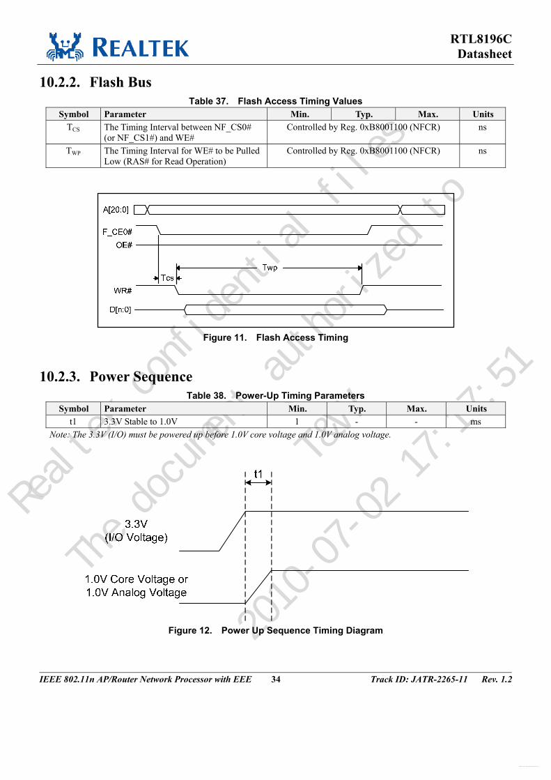
Realtek confidential files
The document authorized to
T&W
2010-07-02 17:17:51
RTL8196C Datasheet
IEEE 802.11n AP/Router Network Processor with EEE 34 Track ID: JATR-2265-11 Rev. 1.2
10.2.2. Flash Bus Table 37. Flash Access Timing Values
Symbol Parameter Min. Typ. Max. Units TCS The Timing Interval between NF_CS0#
(or NF_CS1#) and WE# Controlled by Reg. 0xB8001100 (NFCR) ns
TWP The Timing Interval for WE# to be Pulled Low (RAS# for Read Operation)
Controlled by Reg. 0xB8001100 (NFCR) ns
Figure 11. Flash Access Timing
10.2.3. Power Sequence Table 38. Power-Up Timing Parameters
Symbol Parameter Min. Typ. Max. Units t1 3.3V Stable to 1.0V 1 - - ms
Note: The 3.3V (I/O) must be powered up before 1.0V core voltage and 1.0V analog voltage.
Figure 12. Power Up Sequence Timing Diagram
www.DataSheet.net/
Datasheet pdf - http://www.DataSheet4U.co.kr/

Realtek confidential files
The document authorized to
T&W
2010-07-02 17:17:51
RTL8196C Datasheet
IEEE 802.11n AP/Router Network Processor with EEE 35 Track ID: JATR-2265-11 Rev. 1.2
10.2.4. Power Configuration Timing Power up configuration only relates to internal timing. The external hardware pin reset is irrelevant with regard to power up configuration. The Hardware reset pin is valid when an internal reset ends the active state.
300ms
~
The Latest Stable Power
(1.0V)
CLK (25MHz Crystal)
Config Data(Strapping Pin)
Latch Config Data
Internal Reset200µs
~~ ~
Figure 13. Power Up Configuration Timing Diagram
www.DataSheet.net/
Datasheet pdf - http://www.DataSheet4U.co.kr/

Realtek confidential files
The document authorized to
T&W
2010-07-02 17:17:51
RTL8196C Datasheet
IEEE 802.11n AP/Router Network Processor with EEE 36 Track ID: JATR-2265-11 Rev. 1.2
11. Thermal Characteristics Heat generated by the chip causes a temperature rise of the package. If the temperature of the chip (Tj, junction temperature) is beyond the design limits, there will be negative effects on operation and the life of the IC package. Heat dissipation, either through a heat sink or electrical fan, is necessary to provide a reasonable environment (Ta, ambient temperature) in a closed case. As power density increases, thermal management becomes more critical. A method to estimate the possible Ta is outlined below.
Thermal parameters are defined as below according to JEDEC standard JESD 51-2, 51-6:
(1) θja (Thermal resistance from junction to ambient), represents resistance to heat flow from the chip to ambient air. This is an index of heat dissipation capability. A lower θja means better thermal performance.
θja=(Tj - Ta) / P
Where Tj is the die junction temperature, Ta is the ambient air temperature
P is the power dissipation by device (Watts)
(2) θjc (Thermal Resistance Junction-to-Case, °C/W), measures the heat flow resistance between the die surface and the surface of the package (case). This data is relevant for packages used with external heat sinks.
θjc=(Tj - Tc) / P
Where Tj is the die junction temperature, Tc is the package case temperature
P is the power dissipation by device (Watts)
(3) Ψjt (Thermal Characterization Parameter: Junction to package top), represents the correlation between the temperature of the chip and the package top.
Ψjt=(Tj - Tt) / P
Where Tj is the die junction temperature, Tt is the top of package temperature
P is the power dissipation by device (Watts)
www.DataSheet.net/
Datasheet pdf - http://www.DataSheet4U.co.kr/

Realtek confidential files
The document authorized to
T&W
2010-07-02 17:17:51
RTL8196C Datasheet
IEEE 802.11n AP/Router Network Processor with EEE 37 Track ID: JATR-2265-11 Rev. 1.2
Thermal Terminology The major thermal dissipation paths can be illustrated as follows:
Tj: The maximum junction temperature
Ta: The ambient or environment temperature
Tc: The maximum compound surface temperature
Tb: The maximum surface temperature of PCB bottom
P: Total input power
PQFP Junction to ambient thermal resistance, θja, defined as:
θJA = TJ - TA
P
11.1. Thermal Operating Range Table 39. Thermal Operating Range
Parameter SYM Condition Min Typical Max Units Junction Operating Temperature Tj - 0 - 125 °C Ambient Operating Temperature Ta 4-layer FR4 PCB (without head sink) 0 25 65 °C Note: PCB conditions (JEDEC JESD51-7). Dimensions: 76.2mm x 114.3mm; Thickness: 1.6mm.
11.2. Thermal Parameters Table 40. Thermal Parameters
Parameter SYM Condition Air Flow 0 m/s
Air Flow 1 m/s
Air Flow 2 m/s
Air Flow 3 m/s
Units
Thermal Resistance: Junction to ambient θja 2-layer FR4 PCB 42.7 39.1 37.7 37.1 °C/W Thermal Resistance: Junction to ambient θja 4-layer FR4 PCB 35.4 34 33.4 32.9 °C/W Thermal Characterization: Junction to package top
Ψjt 2-layer FR4 PCB 6.8 7.8 8.3 8.8 °C/W
Thermal Characterization: Junction to package top
Ψjt 4-layer FR4 PCB 4.6 5.3 5.7 5.9 °C/W
Note: PCB conditions (JEDEC JESD51-7): Dimensions: 76.2mm x 114.3mm; Thickness: 1.6mm.
Tj
Tc
Tb •
•
• Ta
Ta
P
Thermal Dissipation of PQFP Package
www.DataSheet.net/
Datasheet pdf - http://www.DataSheet4U.co.kr/

Realtek confidential files
The document authorized to
T&W
2010-07-02 17:17:51
RTL8196C Datasheet
IEEE 802.11n AP/Router Network Processor with EEE 38 Track ID: JATR-2265-11 Rev. 1.2
12. Mechanical Dimensions 12.1. Plastic Quad Flat Package 128-Pin 14x20mm Outline
Symbol Dimension in mm Dimension in inch Min Nom Max Min Nom Max
A - - 3.40 - - 0.134 A1 0.25 - - 0.010 - - A2 2.50 2.70 2.90 0.100 0.106 0.114 b 0.17 0.22 0.27 0.007 0.009 0.011 D 23.2BSC 0.913BSC D1 20.00BSC 0.787BSC E 17.20BSC 0.677BSC E1 14.00BSC 0.551BSC e 0.50BSC 0.020BSC L 0.73 0.88 1.03 0.029 0.035 0.041
L1 1.60REF 0.063REF Notes: CONTROLLING DIMENSION: MILLIMETER (mm).
www.DataSheet.net/
Datasheet pdf - http://www.DataSheet4U.co.kr/
Realtek confidential files
The document authorized to
T&W
2010-07-02 17:17:51
RTL8196C Datasheet
IEEE 802.11n AP/Router Network Processor with EEE 39 Track ID: JATR-2265-11 Rev. 1.2
13. Ordering Information Table 41. Ordering Information
Part Number Package Status RTL8196C-GR 128-Pin PQFP, ‘Green’ Package Mass Production
Note: See page 5 for package and version identification.
Realtek Semiconductor Corp. Headquarters No. 2, Innovation Road II Hsinchu Science Park, Hsinchu, 300, Taiwan, R.O.C. Tel.: +886-3-578-0211. Fax: +886-3-577-6047 www.realtek.com
www.DataSheet.net/
Datasheet pdf - http://www.DataSheet4U.co.kr/