realview platform baseboard for arm1176jzf-s user...
TRANSCRIPT

RealView® Platform Baseboard forARM1176JZF-S
HBI-0147
User Guide
Copyright © 2007-2011 ARM Limited. All rights reserved.ARM DUI 0425F
RealView Platform Baseboard for ARM1176JZF-SUser Guide
Copyright © 2007-2011 ARM Limited. All rights reserved.
Release Information
Proprietary Notice
Words and logos marked with ® or ™ are registered trademarks or trademarks owned by ARM Limited, except as otherwise stated below in this proprietary notice. Other brands and names mentioned herein may be the trademarks of their respective owners.
Neither the whole nor any part of the information contained in, or the product described in, this document may be adapted or reproduced in any material form except with the prior written permission of the copyright holder.
The product described in this document is subject to continuous developments and improvements. All particulars of the product and its use contained in this document are given by ARM in good faith. However, all warranties implied or expressed, including but not limited to implied warranties of merchantability, or fitness for purpose, are excluded.
This document is intended only to assist the reader in the use of the product. ARM Limited shall not be liable for any loss or damage arising from the use of any information in this document, or any error or omission in such information, or any incorrect use of the product.
Confidentiality Status
This document is Non-Confidential. The right to use, copy and disclose this document may be subject to license restrictions in accordance with the terms of the agreement entered into by ARM and the party that ARM delivered this document to.
Unrestricted Access is an ARM internal classification.
Product Status
The information in this document is final, that is for a developed product.
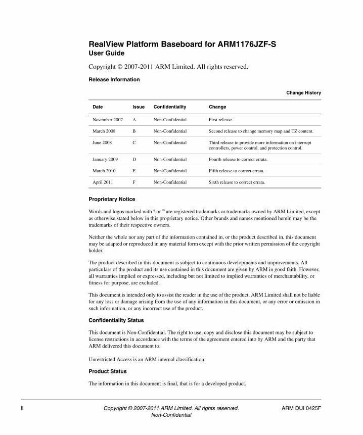
Change History
Date Issue Confidentiality Change
November 2007 A Non-Confidential First release.
March 2008 B Non-Confidential Second release to change memory map and TZ content.
June 2008 C Non-Confidential Third release to provide more information on interrupt controllers, power control, and protection control.
January 2009 D Non-Confidential Fourth release to correct errata.
March 2010 E Non-Confidential Fifth release to correct errata.
April 2011 F Non-Confidential Sixth release to correct errata.
ii Copyright © 2007-2011 ARM Limited. All rights reserved. ARM DUI 0425FNon-Confidential

Web Address
http://www.arm.com
ARM DUI 0425F Copyright © 2007-2011 ARM Limited. All rights reserved. iiiNon-Confidential

Conformance Notices
This section contains conformance notices.
Federal Communications Commission Notice
This device is test equipment and consequently is exempt from part 15 of the FCC Rules under section 15.103 (c).
CE Declaration of Conformity
The system should be powered down when not in use.
The ARM1176JZF-S generates, uses, and can radiate radio frequency energy and may cause harmful interference to radio communications. However, there is no guarantee that interference will not occur in a particular installation. If this equipment causes harmful interference to radio or television reception, which can be determined by turning the equipment off or on, you are encouraged to try to correct the interference by one or more of the following measures:
• ensure attached cables do not lie across the card
• reorient the receiving antenna
• increase the distance between the equipment and the receiver
• connect the equipment into an outlet on a circuit different from that to which the receiver is connected
• consult the dealer or an experienced radio/TV technician for help
Note It is recommended that wherever possible shielded interface cables be used.
iv Copyright © 2007-2011 ARM Limited. All rights reserved. ARM DUI 0425FNon-Confidential
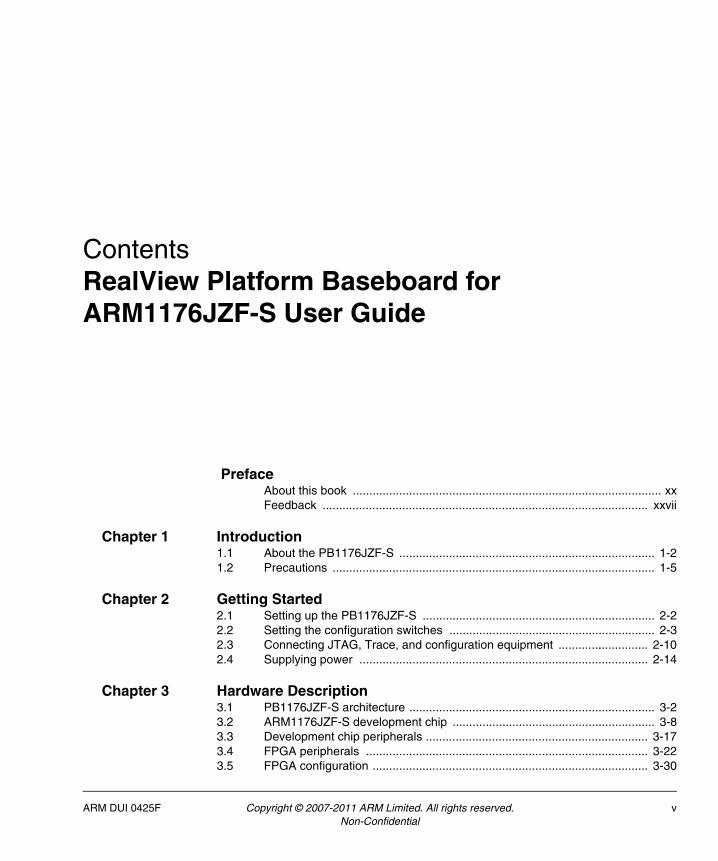
ContentsRealView Platform Baseboard for ARM1176JZF-S User Guide
PrefaceAbout this book ............................................................................................. xxFeedback .................................................................................................. xxvii
Chapter 1 Introduction1.1 About the PB1176JZF-S ............................................................................. 1-21.2 Precautions ................................................................................................. 1-5
Chapter 2 Getting Started2.1 Setting up the PB1176JZF-S ...................................................................... 2-22.2 Setting the configuration switches .............................................................. 2-32.3 Connecting JTAG, Trace, and configuration equipment ........................... 2-102.4 Supplying power ....................................................................................... 2-14
Chapter 3 Hardware Description3.1 PB1176JZF-S architecture .......................................................................... 3-23.2 ARM1176JZF-S development chip ............................................................. 3-83.3 Development chip peripherals ................................................................... 3-173.4 FPGA peripherals ..................................................................................... 3-223.5 FPGA configuration ................................................................................... 3-30
ARM DUI 0425F Copyright © 2007-2011 ARM Limited. All rights reserved. vNon-Confidential

Contents
3.6 Reset controller ........................................................................................ 3-323.7 Power supply ............................................................................................ 3-353.8 Clock architecture ..................................................................................... 3-383.9 Test, configuration, and debug interfaces ................................................ 3-51
Chapter 4 Programmer’s Reference4.1 Memory map ............................................................................................... 4-34.2 ARM1176JZF-S development chip system controller .............................. 4-124.3 Advanced Power Controller and Power Management Interface ............... 4-224.4 Advanced Audio CODEC Interface, AACI ................................................ 4-274.5 Character LCD display ............................................................................. 4-294.6 Color LCD Controller, CLCDC .................................................................. 4-324.7 Dynamic Memory Controller, DMC ........................................................... 4-344.8 Ethernet .................................................................................................... 4-364.9 FPGA status and system control registers ............................................... 4-374.10 General Purpose Input/Output, GPIO ....................................................... 4-574.11 Interrupt controllers in the ARM1176JZF-S development chip ................. 4-584.12 Interrupt controllers in the FPGA .............................................................. 4-744.13 Level 2 Cache Controller ........................................................................ 4-1064.14 Keyboard and Mouse Interface, KMI ...................................................... 4-1074.15 MultiMedia Card Interfaces, MCI ............................................................ 4-1084.16 PCI controller .......................................................................................... 4-1094.17 Real Time Clock, RTC ............................................................................ 4-1204.18 Serial bus interface ................................................................................. 4-1214.19 Smart Card Interface, SCI ...................................................................... 4-1234.20 Synchronous Serial Port, SSP ................................................................ 4-1244.21 Synchronous Static Memory Controller, SSMC ...................................... 4-1264.22 System Controller ................................................................................... 4-1304.23 Timers ..................................................................................................... 4-1314.24 TrustZone Protection Controller ............................................................. 4-1324.25 UART ...................................................................................................... 4-1404.26 USB interface ......................................................................................... 4-1424.27 Watchdog ............................................................................................... 4-143
Appendix A Signal DescriptionsA.1 Synchronous Serial Port interface .............................................................. A-2A.2 Smart Card interface .................................................................................. A-3A.3 UART interface ........................................................................................... A-5A.4 USB interface ............................................................................................. A-6A.5 Audio CODEC interface .............................................................................. A-7A.6 MMC and SD flash card interface ............................................................... A-9A.7 CLCD DVI display interface ...................................................................... A-11A.8 GPIO interface .......................................................................................... A-12A.9 Keyboard and mouse interface ................................................................. A-13A.10 Ethernet interface ..................................................................................... A-14A.11 RealView Logic Tile header connectors ................................................... A-15A.12 Test and debug connections .................................................................... A-16
vi Copyright © 2007-2011 ARM Limited. All rights reserved. ARM DUI 0425FNon-Confidential

Contents
Appendix B SpecificationsB.1 Electrical specification ................................................................................. B-2B.2 Clock rate restrictions .................................................................................. B-4B.3 Mechanical details ...................................................................................... B-5
Appendix C RealView Logic TileC.1 About the RealView Logic Tile ................................................................... C-2C.2 Signals on the tile header connectors ........................................................ C-7
Appendix D PCI Backplane and EnclosureD.1 Connecting the PB1176JZF-S to the PCI enclosure .................................. D-2D.2 Backplane hardware .................................................................................. D-6D.3 Connectors ............................................................................................... D-10
Appendix E Memory Expansion BoardsE.1 About memory expansion ........................................................................... E-2E.2 Fitting a memory board ............................................................................... E-4E.3 Connector pinout ......................................................................................... E-5
Appendix F Boot Monitor and platform libraryF.1 About the Boot Monitor ............................................................................... F-2F.2 About the platform library ............................................................................ F-3F.3 Using the baseboard Boot Monitor and platform library .............................. F-4
Appendix G Boot Monitor CommandsG.1 About Boot Monitor commands .................................................................. G-2G.2 Boot Monitor command set ........................................................................ G-3
Appendix H Loading FPGA ImagesH.1 General procedure ..................................................................................... H-2H.2 Board files .................................................................................................. H-3H.3 The progcards utilities ................................................................................ H-5H.4 Upgrading your hardware .......................................................................... H-6
Glossary
ARM DUI 0425F Copyright © 2007-2011 ARM Limited. All rights reserved. viiNon-Confidential

Contents
viii Copyright © 2007-2011 ARM Limited. All rights reserved. ARM DUI 0425FNon-Confidential

List of TablesRealView Platform Baseboard for ARM1176JZF-S User Guide
Change History ............................................................................................................. iiTable 2-1 Selecting the boot device .......................................................................................... 2-4Table 2-2 Selecting secure debug ............................................................................................. 2-4Table 2-3 Clock frequency selection ......................................................................................... 2-5Table 2-4 FPGA image selection .............................................................................................. 2-5Table 2-5 Default switch position .............................................................................................. 2-6Table 2-6 LED Indicators ........................................................................................................... 2-6Table 2-7 STDIO redirection ..................................................................................................... 2-9Table 3-1 Serial interface signal assignment .......................................................................... 3-21Table 3-2 Serial interface device addresses ........................................................................... 3-26Table 3-3 Reset sources and effects ....................................................................................... 3-33Table 3-4 CFGREMAP signals ................................................................................................ 3-34Table 3-5 FPGA clocks ........................................................................................................... 3-39Table 3-6 ARM1176JZF-S development chip clocks .............................................................. 3-41Table 3-7 ACLKEXTDIVSLV divisor values ............................................................................ 3-45Table 3-8 ACLKEXTDIVMSTR divisor values ......................................................................... 3-46Table 3-9 SMCMEMCLKDIV divisor values ............................................................................ 3-46Table 3-10 JTAG related signals ............................................................................................... 3-55Table 4-1 Memory map ............................................................................................................. 4-4Table 4-2 Development chip system controller registers ......................................................... 4-12Table 4-3 Configuration signals register .................................................................................. 4-14
ARM DUI 0425F Copyright © 2007-2011 ARM Limited. All rights reserved. ixNon-Confidential

List of Tables
Table 4-4 Configuration signals .............................................................................................. 4-15Table 4-5 System Control register .......................................................................................... 4-16Table 4-6 System Status register ............................................................................................ 4-17Table 4-7 PLL Configuration Settings register ........................................................................ 4-19Table 4-8 Example formulas for PLLCFGPERFx registers ..................................................... 4-19Table 4-9 AXIPriority register .................................................................................................. 4-20Table 4-10 SMC Exclusive Access Monitor ID register ............................................................ 4-21Table 4-11 DLL Calibrate Outputs register ............................................................................... 4-21Table 4-12 Power Management Interface and IEM Interface implementation .......................... 4-22Table 4-13 Power Management Interface registers in the FPGA ............................................. 4-23Table 4-14 PWR_CONTROL .................................................................................................... 4-24Table 4-15 PWR_READx registers ........................................................................................... 4-24Table 4-16 PWR_READx content ............................................................................................. 4-24Table 4-17 PWR_AVGx registers ............................................................................................. 4-25Table 4-18 PWR_AVGx content ............................................................................................... 4-25Table 4-19 PWR_MEMx registers ............................................................................................ 4-26Table 4-20 PWR_MEMx content .............................................................................................. 4-26Table 4-21 AACI implementation .............................................................................................. 4-27Table 4-22 Modified AACI PeriphID3 register ........................................................................... 4-28Table 4-23 Character LCD display implementation .................................................................. 4-29Table 4-24 Character LCD control and data registers .............................................................. 4-30Table 4-25 Character LCD display commands ......................................................................... 4-31Table 4-26 CLCDC implementation .......................................................................................... 4-32Table 4-27 PrimeCell CLCDC register differences ................................................................... 4-33Table 4-28 Values for different display resolutions ................................................................... 4-33Table 4-29 DMC implementation .............................................................................................. 4-34Table 4-30 SDRAM register values .......................................................................................... 4-34Table 4-31 Ethernet implementation ......................................................................................... 4-36Table 4-32 Register map for FPGA System Controller registers .............................................. 4-37Table 4-33 ID Register, SYS_ID bit assignment ....................................................................... 4-41Table 4-34 Oscillator Register, SYS_OSCx bit assignment ..................................................... 4-42Table 4-35 Default values for oscillators ................................................................................... 4-43Table 4-36 Lock Register, SYS_LOCK bit assignment ............................................................. 4-44Table 4-37 SYS-CFGDATA 1 register ...................................................................................... 4-45Table 4-38 SYS-CFGDATA 2 register ...................................................................................... 4-47Table 4-39 Flag registers .......................................................................................................... 4-48Table 4-40 Reset level control .................................................................................................. 4-49Table 4-41 PCI bus status ........................................................................................................ 4-50Table 4-42 Flash control ........................................................................................................... 4-50Table 4-43 SYS_CLCD register ................................................................................................ 4-51Table 4-44 BOOT configuration switches ................................................................................. 4-51Table 4-45 SYS_MISC .............................................................................................................. 4-52Table 4-46 SYS_BUSID ............................................................................................................ 4-53Table 4-47 System status registers .......................................................................................... 4-54Table 4-48 Oscillator test registers ........................................................................................... 4-56Table 4-49 GPIO implementation ............................................................................................. 4-57Table 4-50 TZIC implementation in development chip ............................................................. 4-58
x Copyright © 2007-2011 ARM Limited. All rights reserved. ARM DUI 0425FNon-Confidential

List of Tables
Table 4-51 TZIC register summary ........................................................................................... 4-59Table 4-52 TZICFIQStatus Register bit assignments ................................................................ 4-60Table 4-53 TZICRawIntr Register bit assignments ................................................................... 4-60Table 4-54 TZICIntSelect Register bit assignments .................................................................. 4-61Table 4-55 TZICFIQEnable Register bit assignments ............................................................... 4-61Table 4-56 TZICFIQEnClear Register bit assignments ............................................................. 4-62Table 4-57 TZICFIQBypass Register bit assignments .............................................................. 4-63Table 4-58 TZICProtection Register bit assignments ................................................................ 4-64Table 4-59 TZICLock Register bit assignments ........................................................................ 4-64Table 4-60 TZICLockStatus Register bit assignments .............................................................. 4-65Table 4-61 TZICPeriphlD0-3 Register bit assignments ............................................................. 4-65Table 4-62 TZICPeriphID0 Register bit assignments ................................................................ 4-66Table 4-63 TZICPeriphID1 Register bit assignments ................................................................ 4-67Table 4-64 TZICPeriphID2 Register bit assignments ................................................................ 4-67Table 4-65 TZICPeriphID3 Register bit assignments ................................................................ 4-68Table 4-66 TZICPCellID0 Register bit assignments .................................................................. 4-68Table 4-67 TZICPCellID1 Register bit assignments .................................................................. 4-69Table 4-68 TZICPCellID2 Register bit assignments .................................................................. 4-69Table 4-69 TZICPCellID3 Register bit assignments .................................................................. 4-69Table 4-70 GIC implementation in development chip ............................................................... 4-70Table 4-71 Interrupt signals to development chip interrupt controllers ...................................... 4-72Table 4-72 GIC implementation in FPGA .................................................................................. 4-74Table 4-73 Interrupt signals to FPGA primary and secondary GICs ......................................... 4-75Table 4-74 FPGA Register summary ........................................................................................ 4-77Table 4-75 Distributor Register Control Register bit assignments ............................................. 4-79Table 4-76 Interrupt Controller Type Register bit assignments ................................................. 4-79Table 4-77 Interrupt Set-Enable Register 0 bit assignments ..................................................... 4-80Table 4-78 Interrupt Set-Enable Register 1 bit assignments ..................................................... 4-81Table 4-79 Interrupt Clear-Enable Register 0 bit assignments ................................................. 4-82Table 4-80 Interrupt Clear-Enable Register 1 bit assignments ................................................. 4-82Table 4-81 Interrupt Set-Pending Register 0 bit assignments ................................................... 4-83Table 4-82 Interrupt Set-Pending Register 1 bit assignments ................................................... 4-84Table 4-83 Interrupt Clear-Pending Register 0 bit assignments ............................................... 4-85Table 4-84 Interrupt Clear-Pending Register 1 bit assignments ............................................... 4-85Table 4-85 Active Bit Register 0 and 1 bit assignments ............................................................ 4-86Table 4-86 Interrupt Priority Register 0-3 bit assignments ........................................................ 4-88Table 4-87 Interrupt Priority Register 4-6 bit assignments ........................................................ 4-89Table 4-88 Interrupt Priority 7-15 Register bit assignments ...................................................... 4-90Table 4-89 Interrupt CPU Target Registers 0-6 bit assignments ............................................... 4-91Table 4-90 Interrupt CPU Target Register 7 bit assignments ................................................... 4-91Table 4-91 Interrupt CPU Target Register 8-15 bit assignments .............................................. 4-93Table 4-92 Interrupt Configuration Register 0 bit definition ....................................................... 4-94Table 4-93 IT[0] interrupt definition encoding ............................................................................ 4-95Table 4-94 IT[1] interrupt definition encoding ............................................................................ 4-95Table 4-95 Interrupt Configuration Register 1 bit assignments ................................................. 4-97Table 4-96 Interrupt Configuration Register 2-3 bit definition .................................................... 4-98Table 4-97 Software Interrupt Register bit definition ................................................................. 4-99
ARM DUI 0425F Copyright © 2007-2011 ARM Limited. All rights reserved. xiNon-Confidential

List of Tables
Table 4-98 CPU interface registers ......................................................................................... 4-101Table 4-99 CPU Interface Control register bit assignments .................................................... 4-101Table 4-100 Priority Mask Register bit assignments ................................................................. 4-102Table 4-101 Binary Pointer Register bit assignments ............................................................... 4-102Table 4-102 Binary Point value meanings ................................................................................ 4-102Table 4-103 Interrupt Acknowledge Register bit assignments .................................................. 4-103Table 4-104 End of Interrupt Register bit assignments ............................................................. 4-104Table 4-105 Running interrupt Register bit assignments .......................................................... 4-104Table 4-106 Highest Pending interrupt Register bit assignments ............................................. 4-105Table 4-107 L2CC implementation in development chip .......................................................... 4-106Table 4-108 KMI implementation .............................................................................................. 4-107Table 4-109 MCI implementation .............................................................................................. 4-108Table 4-110 PCI controller implementation ............................................................................... 4-109Table 4-111 PCI bus memory map for AXI M bridge ................................................................ 4-110Table 4-112 PCI controller registers ......................................................................................... 4-110Table 4-113 PCI_IMAP0 register format ................................................................................... 4-111Table 4-114 PCI_IMAP1 register format ................................................................................... 4-111Table 4-115 PCI_IMAP2 register format ................................................................................... 4-112Table 4-116 PCI_SELFID register format ................................................................................. 4-112Table 4-117 PCI_FLAGS register format .................................................................................. 4-113Table 4-118 PCI_SMAPx register format .................................................................................. 4-114Table 4-119 PCI backplane configuration header addresses (self-config) ............................... 4-115Table 4-120 PCI backplane configuration header addresses (normal configuration) ............... 4-115Table 4-121 PCI configuration space header ........................................................................... 4-116Table 4-122 PCI bus commands supported ............................................................................. 4-119Table 4-123 RTC implementation ............................................................................................. 4-120Table 4-124 Serial bus implementation .................................................................................... 4-121Table 4-125 Serial bus register ................................................................................................. 4-121Table 4-126 Serial bus device addresses ................................................................................. 4-122Table 4-127 SCI implementation .............................................................................................. 4-123Table 4-128 SSP implementation ............................................................................................. 4-124Table 4-129 SSMC implementation .......................................................................................... 4-126Table 4-130 Register values for NOR2 ..................................................................................... 4-127Table 4-131 Register values for Intel flash, standard async read mode, no bursts .................. 4-127Table 4-132 Register values for Intel flash, async page mode ................................................. 4-128Table 4-133 Register values for Samsung SRAM .................................................................... 4-128Table 4-134 Register values for Spansion BDS640 ................................................................. 4-128Table 4-135 Register values for Spansion LV256 .................................................................... 4-129Table 4-136 System controller implementation ......................................................................... 4-130Table 4-137 Timer implementation ........................................................................................... 4-131Table 4-138 TrustZone Protection Controller implementation .................................................. 4-132Table 4-139 FPGA TrustZone Protection Controller registers .................................................. 4-133Table 4-140 FPGA TZPCDECPROT0x bit assignment ............................................................ 4-134Table 4-141 FPGA TZPCDECPROT1x bit assignment ............................................................ 4-134Table 4-142 FPGA TZPCDECPROT2 register ......................................................................... 4-135Table 4-143 Development chip TrustZone Protection Controller registers ............................... 4-135Table 4-144 Development chip TZPCDECPROT0x bit assignment ......................................... 4-137
xii Copyright © 2007-2011 ARM Limited. All rights reserved. ARM DUI 0425FNon-Confidential

List of Tables
Table 4-145 Development chip TZPCDECPROT1x bit assignment .......................................... 4-138Table 4-146 Development chip TZPCDECPROT2 ................................................................... 4-139Table 4-147 UART implementation ........................................................................................... 4-140Table 4-148 USB implementation ............................................................................................. 4-142Table 4-149 USB controller base address ................................................................................ 4-142Table 4-150 Watchdog implementation ..................................................................................... 4-143Table A-1 SSP signal assignment ............................................................................................. A-2Table A-2 Smartcard connector signal assignment ................................................................... A-3Table A-3 Signals on SCI expansion connector ........................................................................ A-4Table A-4 Serial plug signal assignment ................................................................................... A-5Table A-5 USB signals ............................................................................................................... A-6Table A-6 Audio CODEC expansion connector signals ............................................................. A-7Table A-7 Multimedia Card interface signals ........................................................................... A-10Table A-8 DVI Digital/Analog connector signals ...................................................................... A-11Table A-9 Mouse and keyboard port signal descriptions ......................................................... A-13Table A-10 Ethernet signals ...................................................................................................... A-14Table A-11 Trace connector J2 ................................................................................................. A-18Table A-12 Trace connector J3 ................................................................................................. A-19Table A-13 Logic Tile trace connector J7 .................................................................................. A-20Table B-1 PB1176JZF-S electrical characteristics .................................................................... B-2Table B-2 Current requirements from DC IN (12V) .................................................................... B-2Table B-3 Current requirements from terminal connector .......................................................... B-3Table B-4 Maximum current load on supply voltage rails .......................................................... B-3Table C-1 RealView Logic Tile clock signals ............................................................................ C-5Table C-2 Reset signal descriptions ......................................................................................... C-6Table C-3 HDRX signals ........................................................................................................... C-8Table C-4 HDRY signals ......................................................................................................... C-14Table C-5 HDRZ signals ......................................................................................................... C-20Table D-1 LED indicators .......................................................................................................... D-7Table D-2 Configuration switches ............................................................................................. D-8Table D-3 Power and reset switches ........................................................................................ D-8Table D-4 Test points ................................................................................................................ D-8Table D-5 ATX power connector ............................................................................................. D-10Table D-6 Mictor connector pinout .......................................................................................... D-11Table E-1 Static memory connector signals .............................................................................. E-5Table F-1 STDIO redirection ..................................................................................................... F-5Table F-2 platform library options ............................................................................................ F-11Table F-3 NFU commands ...................................................................................................... F-16Table F-4 NFU MANAGE commands ...................................................................................... F-17Table G-1 Standard Boot Monitor command set ....................................................................... G-3Table G-2 MMC and SD card sub-menu commands ................................................................ G-4Table G-3 Boot Monitor Configure commands .......................................................................... G-5Table G-4 Boot Monitor Debug commands ............................................................................... G-6Table G-5 Boot Monitor NOR flash commands ......................................................................... G-7
ARM DUI 0425F Copyright © 2007-2011 ARM Limited. All rights reserved. xiiiNon-Confidential

List of Tables
xiv Copyright © 2007-2011 ARM Limited. All rights reserved. ARM DUI 0425FNon-Confidential

List of FiguresRealView Platform Baseboard for ARM1176JZF-S User Guide
Key to timing diagram conventions ........................................................................... xxiiFigure 2-1 Location of S7, S1 and S6 ........................................................................................ 2-3Figure 2-2 JTAG, Trace, and config connectors ....................................................................... 2-10Figure 2-3 Power connectors ................................................................................................... 2-14Figure 3-1 PB1176JZF-S layout ................................................................................................. 3-3Figure 3-2 PB1176JZF-S block diagram .................................................................................... 3-4Figure 3-3 ARM1176JZF-S development chip block diagram .................................................... 3-9Figure 3-4 AXI master bus multiplexing .................................................................................... 3-14Figure 3-5 Memory devices ...................................................................................................... 3-18Figure 3-6 Interrupt controller block diagram ............................................................................ 3-19Figure 3-7 FPGA block diagram ............................................................................................... 3-23Figure 3-8 PCI bridge ............................................................................................................... 3-28Figure 3-9 Voltage control and voltage and current monitoring ................................................ 3-37Figure 3-10 Clock architecture for PB1176JZF-S ....................................................................... 3-38Figure 3-11 Development chip clocks ........................................................................................ 3-40Figure 3-12 DCG clock selection and divider logic ..................................................................... 3-43Figure 3-13 Serial data and SYS_OSCx register format ............................................................ 3-49Figure 3-14 JTAG data paths in debug mode ............................................................................ 3-52Figure 3-15 JTAG data paths in debug mode with ILA ............................................................... 3-52Figure 3-16 JTAG data paths in config mode ............................................................................. 3-53Figure 4-1 Memory map ........................................................................................................... 4-11
ARM DUI 0425F Copyright © 2007-2011 ARM Limited. All rights reserved. xvNon-Confidential

List of Figures
Figure 4-2 PLLCFGPERFx registers ........................................................................................ 4-19Figure 4-3 AACI ID register ...................................................................................................... 4-27Figure 4-4 ID Register, SYS_ID ............................................................................................... 4-40Figure 4-5 SYS_SW ................................................................................................................. 4-41Figure 4-6 SYS_LED ................................................................................................................ 4-41Figure 4-7 Oscillator Register, SYS_OSCx .............................................................................. 4-42Figure 4-8 Lock Register, SYS_LOCK ..................................................................................... 4-43Figure 4-9 SYS_RESETCTL .................................................................................................... 4-49Figure 4-10 SYS_CLCD ............................................................................................................. 4-51Figure 4-11 SYS_BOOTCS ....................................................................................................... 4-51Figure 4-12 SYS_MISC .............................................................................................................. 4-52Figure 4-13 Oscillator Register, SYS_OSCRESETx .................................................................. 4-55Figure 4-14 TZICFIQBypass Register bit assignments .............................................................. 4-63Figure 4-15 TZICProtection Register bit assignments ............................................................... 4-63Figure 4-16 TZICLockStatus Register bit assignments .............................................................. 4-64Figure 4-17 TZICPeriphlD0-3 registers bit assignments ............................................................ 4-65Figure 4-18 TZICPeriphlDO Register bit assignments ............................................................... 4-66Figure 4-19 TZICPeriphlD1 Register bit assignments ................................................................ 4-66Figure 4-20 TZICPeriphlD2 Register bit assignments ................................................................ 4-67Figure 4-21 TZICPeriphlD3 Register bit assignments ................................................................ 4-68Figure 4-22 TZICPCelllD0-3 Registers bit assignments ............................................................ 4-68Figure 4-23 Distributor Register Control Register bit assignments ............................................ 4-78Figure 4-24 Interrupt Controller Type Register bit assignments ................................................ 4-79Figure 4-25 Interrupt Set-Enable Register 0 bit assignments .................................................... 4-80Figure 4-26 Interrupt Set-Enable Register 1 bit assignments .................................................... 4-81Figure 4-27 Interrupt Clear-Enable Register 0 bit assignments ................................................. 4-81Figure 4-28 Interrupt Clear-Enable Register 1 bit assignments ................................................. 4-82Figure 4-29 Interrupt Set-Pending Register 0 bit assignments .................................................. 4-83Figure 4-30 Interrupt Set-Pending Register 1 bit assignments .................................................. 4-83Figure 4-31 Interrupt Clear-Pending Register 0 bit assignments ............................................... 4-85Figure 4-32 Interrupt Clear-Pending Register 1 bit assignments ............................................... 4-85Figure 4-33 Active Bit Register 0 and 1 bit assignments ........................................................... 4-86Figure 4-34 Interrupt Priority Register 0-3 bit assignments ........................................................ 4-87Figure 4-35 Interrupt Priority Register 4-6 bit assignments ........................................................ 4-88Figure 4-36 Interrupt Priority Register 7-15 bit assignments ...................................................... 4-89Figure 4-37 Interrupt CPU Target Registers 0-6 bit assignments .............................................. 4-90Figure 4-38 Interrupt CPU Target Register 7 bit assignments ................................................... 4-91Figure 4-39 Interrupt CPU Target Register 8-15 ........................................................................ 4-92Figure 4-40 Interrupt Configuration Register 0 bit assignments ................................................. 4-94Figure 4-41 Interrupt Configuration Register 1 bit assignments ................................................. 4-96Figure 4-42 Interrupt Configuration Register 2-3 bit assignments ............................................. 4-98Figure 4-43 Software Interrupt Register bit assignments ........................................................... 4-99Figure 4-44 AXI M to PCI mapping .......................................................................................... 4-111Figure 4-45 PCI_SELFID register ............................................................................................ 4-112Figure 4-46 PCI_FLAGS register ............................................................................................. 4-113Figure 4-47 PCI to AXI S mapping ........................................................................................... 4-114Figure 4-48 PCI_SMAPx register ............................................................................................. 4-114
xvi Copyright © 2007-2011 ARM Limited. All rights reserved. ARM DUI 0425FNon-Confidential

List of Figures
Figure 4-49 Secure and non-secure internal RAM ................................................................... 4-137Figure A-1 SSP expansion interface ........................................................................................... A-2Figure A-2 Smartcard contacts assignment ................................................................................ A-3Figure A-3 SCI expansion connector J29 ................................................................................... A-4Figure A-4 Serial connector for J26A, J26B, J27A, and J27B .................................................... A-5Figure A-5 USB interfaces .......................................................................................................... A-6Figure A-6 Audio connectors ...................................................................................................... A-7Figure A-7 AACI expansion connector ........................................................................................ A-8Figure A-8 MMC/SD card socket pin numbering ........................................................................ A-9Figure A-9 MMC card .................................................................................................................. A-9Figure A-10 DVI Digital/Analog connector .................................................................................. A-11Figure A-11 GPIO connector ...................................................................................................... A-12Figure A-12 KMI connector ......................................................................................................... A-13Figure A-13 Ethernet connector J5 ............................................................................................. A-14Figure A-14 RealView Logic Tile HDRX, HDRY, and HDRZ pin numbering ............................... A-15Figure A-15 Test points and debug connectors .......................................................................... A-16Figure A-16 JTAG connector J12 ............................................................................................... A-17Figure A-17 USB debug connector J15 ...................................................................................... A-18Figure A-18 AMP Mictor connector ............................................................................................. A-18Figure A-19 Integrated logic analyzer connector J11 ................................................................. A-21Figure B-1 Baseboard mechanical details .................................................................................. B-5Figure C-1 AXI busses on Logic Tile .......................................................................................... C-3Figure C-2 JTAG signals to Logic Tiles ...................................................................................... C-4Figure C-3 Power-on reset and configuration timing .................................................................. C-6Figure C-4 HDRX, HDRY, and HDRZ pin numbering ................................................................ C-7Figure D-1 Installing the platform board into the PCI enclosure ................................................ D-3Figure D-2 Multiple boards on PCI bus ...................................................................................... D-5Figure D-3 PCI backplane .......................................................................................................... D-6Figure D-4 JTAG signal flow on the PCI backplane ................................................................... D-9Figure D-5 AMP Mictor connector J4 ....................................................................................... D-11Figure D-6 PCI expansion board JTAG connector J5 .............................................................. D-12Figure E-1 Static memory board block diagram .......................................................................... E-2Figure E-2 Samtec QSH 120-way static expansion connector ................................................... E-5
ARM DUI 0425F Copyright © 2007-2011 ARM Limited. All rights reserved. xviiNon-Confidential

List of Figures
xviii Copyright © 2007-2011 ARM Limited. All rights reserved. ARM DUI 0425FNon-Confidential

Preface
This preface introduces the RealView® Platform Baseboard for ARM1176JZF-S User Guide. It contains the following sections:
• About this book on page xx
• Feedback on page xxvii.
ARM DUI 0425F Copyright © 2007-2011 ARM Limited. All rights reserved. xixNon-Confidential

Preface
About this book
This book describes how to set up and use the RealView Platform Baseboard for ARM1176JZF-S (PB1176JZF-S).
Intended audience
This document has been written for experienced hardware and software developers to aid the development of ARM-based products using the PB1176JZF-S as part of a development system.
Using this book
This book is organized into the following chapters:
Chapter 1 Introduction
Read this chapter for an introduction to the PB1176JZF-S. This chapter shows the physical layout of the board and identifies the main components.
Chapter 2 Getting Started
Read this chapter for a description of how to set up and start using the PB1176JZF-S. This chapter describes how to connect the add-on boards and how to apply power.
Chapter 3 Hardware Description
Read this chapter for a description of the hardware architecture of the PB1176JZF-S. This chapter describes the peripherals, clocks, resets, and debug hardware provided by the board.
Chapter 4 Programmer’s Reference
Read this chapter for a description of the PB1176JZF-S memory map and registers. There is also basic information on the peripherals and controllers present on the Platform Baseboard.
Appendix A Signal Descriptions
See this appendix for a description of the signals on the connectors.
Appendix B Specifications
See this appendix for electrical, timing, and mechanical specifications.
Appendix C RealView Logic Tile
See this appendix for information about the optional Logic Tile.
xx Copyright © 2007-2011 ARM Limited. All rights reserved. ARM DUI 0425FNon-Confidential

Preface
Appendix D PCI Backplane and Enclosure
See this appendix for details of the PCI backplane board.
Appendix E Memory Expansion Boards
See this appendix for details of the memory expansion boards.
Appendix F Boot Monitor and platform library
See this appendix for details on using the supplied Boot Monitor utilities.
Appendix G Boot Monitor Commands
See this appendix for a list of Boot Monitor commands.
Appendix H Loading FPGA Images
See this appendix for details on loading new FPGA images.
Product revision status
The rnpnvn identifier indicates the revision status of products, such as PrimeCells, described in this document, where:
rn Identifies the major revision of the product.
pn Identifies the minor revision or modification status of the product.
vn Identifies a version that does not affect the external functionality of the product.
Typographical conventions
The following typographical conventions are used in this book:
italic Highlights important notes, introduces special terminology, denotes internal cross-references, and citations.
bold Highlights interface elements, such as menu names. Denotes ARM processor signal names. Also used for terms in descriptive lists, where appropriate.
monospace Denotes text that can be entered at the keyboard, such as commands, file and program names, and source code.
monospace Denotes a permitted abbreviation for a command or option. The underlined text can be entered instead of the full command or option name.
ARM DUI 0425F Copyright © 2007-2011 ARM Limited. All rights reserved. xxiNon-Confidential

Preface
monospace italic Denotes arguments to commands and functions where the argument is to be replaced by a specific value.
monospace bold Denotes language keywords when used outside example code.
Other conventions
This document uses other conventions. They are described in the following sections:
• Timing diagrams
• Signals on page xxiii
• Bytes, Halfwords, and Words on page xxiii
• Bits, bytes, k, and M on page xxiii
• Register fields on page xxiv.
• Numbering on page xxiv.
Timing diagrams
The figure named Key to timing diagram conventions explains the components used in timing diagrams. Variations, when they occur, have clear labels. You must not assume any timing information that is not explicit in the diagrams.
Shaded bus and signal areas are undefined, so the bus or signal can assume any value within the shaded area at that time. The actual level is unimportant and does not affect normal operation.
Key to timing diagram conventions
Clock
HIGH to LOW
Transient
HIGH/LOW to HIGH
Bus stable
Bus to high impedance
Bus change
High impedance to stable bus
xxii Copyright © 2007-2011 ARM Limited. All rights reserved. ARM DUI 0425FNon-Confidential
Preface
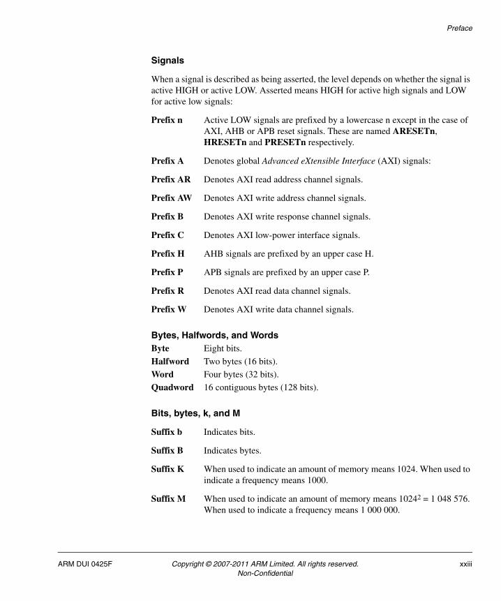
Signals
When a signal is described as being asserted, the level depends on whether the signal is active HIGH or active LOW. Asserted means HIGH for active high signals and LOW for active low signals:
Prefix n Active LOW signals are prefixed by a lowercase n except in the case of AXI, AHB or APB reset signals. These are named ARESETn, HRESETn and PRESETn respectively.
Prefix A Denotes global Advanced eXtensible Interface (AXI) signals:
Prefix AR Denotes AXI read address channel signals.
Prefix AW Denotes AXI write address channel signals.
Prefix B Denotes AXI write response channel signals.
Prefix C Denotes AXI low-power interface signals.
Prefix H AHB signals are prefixed by an upper case H.
Prefix P APB signals are prefixed by an upper case P.
Prefix R Denotes AXI read data channel signals.
Prefix W Denotes AXI write data channel signals.
Bytes, Halfwords, and WordsByte Eight bits.
Halfword Two bytes (16 bits).
Word Four bytes (32 bits).
Quadword 16 contiguous bytes (128 bits).
Bits, bytes, k, and M
Suffix b Indicates bits.
Suffix B Indicates bytes.
Suffix K When used to indicate an amount of memory means 1024. When used to indicate a frequency means 1000.
Suffix M When used to indicate an amount of memory means 10242 = 1 048 576. When used to indicate a frequency means 1 000 000.
ARM DUI 0425F Copyright © 2007-2011 ARM Limited. All rights reserved. xxiiiNon-Confidential
Preface
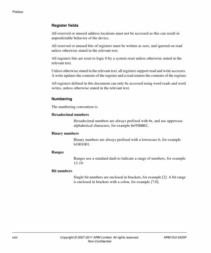
Register fields
All reserved or unused address locations must not be accessed as this can result in unpredictable behavior of the device.
All reserved or unused bits of registers must be written as zero, and ignored on read unless otherwise stated in the relevant text.
All registers bits are reset to logic 0 by a system reset unless otherwise stated in the relevant text.
Unless otherwise stated in the relevant text, all registers support read and write accesses. A write updates the contents of the register and a read returns the contents of the register.
All registers defined in this document can only be accessed using word reads and word writes, unless otherwise stated in the relevant text.
Numbering
The numbering convention is:
Hexadecimal numbers
Hexadecimal numbers are always prefixed with 0x, and use uppercase alphabetical characters, for example 0xFFDD00CC.
Binary numbers
Binary numbers are always prefixed with a lowercase b, for example b1001001.
Ranges
Ranges use a standard dash to indicate a range of numbers, for example 12-19.
Bit numbers
Single bit numbers are enclosed in brackets, for example [2]. A bit range is enclosed in brackets with a colon, for example [7:0].
xxiv Copyright © 2007-2011 ARM Limited. All rights reserved. ARM DUI 0425FNon-Confidential

Preface
Further reading
This section lists related publications by ARM and third parties.
See http://infocenter.arm.com.help/index.jsp for access to ARM documentation.
This book contains information that is specific to this product. See the following documents for other relevant information:
• ARM1176JZF-S Technical Reference Manual (ARM DDI 0301)
• AMBA® Specification (ARM IHI 0011)
• AMBA AXI Protocol (ARM IHI 0022)
• ARM Architecture Reference Manual (ARM DDI 0100)
• ARM PrimeCell Color LCD Controller (PL111) Technical Reference Manual (ARM DDI 0293)
• ARM CoreSight Technology System Design Guide (ARM DGI 0012)
• ARM CoreSight ETM11 Technical Reference Manual (ARM DDI 0318)
• ARM Dual-Timer Module (SP804) Technical Reference Manual (ARM DDI 0271)
• ARM ETB11 Technical Reference Manual (ARM DDI 0275)
• ARM Intelligent Energy Controller Technical Overview (ARM DTO 0005)
• ARM L220 Cache Controller Technical Reference Manual (ARM DDI 0329)
• ARM PrimeCell Advanced Audio CODEC Interface (PL041) Technical Reference Manual (ARM DDI 0173)
• ARM PrimeCell AXI Configurable Interconnect (PL300) Technical Reference Manual (ARM DDI 0354)
• ARM PrimeCell Dynamic Memory Controller (PL340) Technical Reference Manual (ARM DDI 0331)
• ARM PrimeCell General Purpose Input/Output (PL061) Technical Reference Manual (ARM DDI 0190)
• ARM PrimeCell Infrastructure AMBA 3 TrustZone Protection Controller (BP147) Technical Overview (ARM DTO 0015)
• ARM PrimeCell PS2 Keyboard/Mouse Interface (PL050) Technical Reference Manual (ARM DDI 0143)
• ARM PrimeCell Multimedia Card Interface (PL180) Technical Reference Manual (ARM DDI 0172)
• ARM PrimeCell Real Time Clock (PL031) Technical Reference Manual (ARM DDI 0224)
• ARM PrimeCell Smart Card Interface (PL131) Technical Reference Manual (ARM DDI 0228)
• ARM PrimeCell Synchronous Serial Port (PL022) Technical Reference Manual (ARM DDI 0194)
ARM DUI 0425F Copyright © 2007-2011 ARM Limited. All rights reserved. xxvNon-Confidential

Preface
• ARM PrimeCell Synchronous Static Memory Controller (PL093) Technical Reference Manual (ARM DDI 0236)
• ARM PrimeCell UART (PL011) Technical Reference Manual (ARM DDI 0183)
• ARM VFP11 Vector Floating-point Coprocessor Technical Reference Manual (ARM DDI 0274)
• ARM Watchdog Module (SP805) Technical Reference Manual (ARM DDI 0270)
• ARM PrimeCell Infrastructure AMBA 3 AXI to AMBA 2 AHB Bridges (BP137) Technical Overview (ARM DTO 0010).
The following publications provide information about related ARM products and toolkits:
• RealView® ICE and RealView Trace User Guide (ARM DUI 0155)
• Trace Debug Tools User Guide (ARM DUI 0118)
• ARM Versatile/LT-XC2V4000+ User Guide (ARM DUI 0186)
• RealView Debugger User Guide (ARM DUI 0153)
• RealView Compilation Tools Compiler and Libraries Guide (ARM DUI 0205)
• RealView Compilation Tools Developer Guide (ARM DUI 0203)
• RealView Compilation Tools Linker and Utilities Guide (ARM DUI 0206).
xxvi Copyright © 2007-2011 ARM Limited. All rights reserved. ARM DUI 0425FNon-Confidential

Preface
Feedback
ARM® Limited welcomes feedback both on the PB1176JZF-S and on the documentation.
Feedback on this product
If you have any comments or suggestions about this product, contact your supplier giving:
• the product name
• a concise explanation of your comments.
Feedback on this manual
If you have any comments about this document, send email to [email protected] giving:
• the title
• the number
• the relevant page number(s) to which your comments apply
• a concise explanation of your comments.
ARM® Limited also welcomes general suggestions for additions and improvements.
ARM DUI 0425F Copyright © 2007-2011 ARM Limited. All rights reserved. xxviiNon-Confidential

Preface
xxviii Copyright © 2007-2011 ARM Limited. All rights reserved. ARM DUI 0425FNon-Confidential

Chapter 1 Introduction
This chapter introduces the PB1176JZF-S. It contains the following sections:
• About the PB1176JZF-S on page 1-2
• Precautions on page 1-5.
ARM DUI 0425F Copyright © 2007-2011 ARM Limited. All rights reserved. 1-1Non-Confidential

Introduction
1.1 About the PB1176JZF-S
The Platform Baseboard for ARM1176JZF-S is a software and hardware development board based on ARM architecture v6:
• If the baseboard is used on its own, it is a fast software development platform with an ARM1176JZF processor and a memory system running at ASIC speed.
The basic system provides a good platform for developing systems supporting ARM11 processors that feature TrustZone® Technology, CoreSight™, and Intelligent Energy Management (IEM™). The ARM1176JZF-S development chip is much faster than a software simulator or a core implemented in RealView Logic Tiles.
• If FPGA-based RealView Logic Tiles are stacked on the Platform Baseboard, custom AMBA v3 peripherals, processors and DSPs can be added to the ARM subsystem provided by the baseboard.
The expanded system can be used to develop Advanced Microprocessor Bus Architecture (AMBA®) compatible peripherals and to test ASIC designs. The fast processor core and the peripherals present in the ARM1176JZF-S development chip, PB1176JZF-S FPGA, and RealView Logic Tile FPGA enable you to develop and test complex systems operating at, or near, their target operating frequency.
The major components in the PB1176JZF-S are:
• the ARM1176JZF-S development chip
• an FPGA containing additional peripherals and controllers
• 128MB of 32-bit wide Mobile DDR RAM
• 8MB of 32-bit wide static PSRAM
• 2 x 64MB of 32-bit wide NOR flash
• up to 320MB of static memory in an optional PISMO™static memory expansion board
• programmable clock generators
• Time-Of-Year (TOY) clock with backup battery
• connectors for VGA, color LCD display(CLCD) interface board, PCI, UART, GPIO, keyboard/mouse, Smart Card, USB, audio, MMC, SSP, and Ethernet
• RealView Logic Tile connector for one or more optional RealView Logic Tiles to develop custom IP
• debug and test connectors for JTAG, ChipScope, and CoreSight Trace port
• DIP switches and LEDs
• 2 row by 16 character LCD display
• power conversion and voltage control circuitry
1-2 Copyright © 2007-2011 ARM Limited. All rights reserved. ARM DUI 0425FNon-Confidential

Introduction
1.1.1 Baseboard expansion
You can expand the PB1176JZF-S by adding:
• RealView® Logic Tiles containing custom IP
• RealView Core Tiles containing ARM processor test chips
• a PCI expansion enclosure
• static memory expansion board (PISMO)
• VGA monitor or CLCD adaptor and CLCD display
• MMC, SD, or SIM cards
• custom devices to the 16-bit GPIO
• USB devices to the single OTG port and the two standard Host USB ports
• serial devices to the synchronous serial port and the five UARTs (two with full handshake)
• keyboard and mouse
• audio devices to the onboard Audio CODEC
• an Ethernet network to the onboard Ethernet controller.
1.1.2 About the ARM1176JZF-S development chip
The ARM1176JZF-S processor includes an integer core that implements the ARM11 ARM architecture v6. The processor supports:
• the ARM and Thumb® instruction sets
• Jazelle® technology to enable direct execution of Java bytecodes
• Single Instruction Multiple Data (SIMD) DSP instructions
• Vector Floating Point coprocessor (VFP), supporting the ARM VFPv2 floating point coprocessor instruction set
• TrustZone security extensions and TrustZone interrupt controller
• Intelligent Energy Management (IEM)
Note Some features of the IEM subsystem require a separate license for the APC
component.
• Tightly-Coupled Memory (TCM) for code (8KB) and data (8KB)
• AXI secure memory (512KB)
• Memory Management Unit (MMU)
ARM DUI 0425F Copyright © 2007-2011 ARM Limited. All rights reserved. 1-3Non-Confidential

Introduction
• System Controller
• Vectored Interrupt Port
• Embedded-ICE-RT logic for JTAG debugging
• Level 2 Cache and Controller with 128KB unified cache
• Dynamic Memory Controller (DMC) supporting 32-bit Mobile DDR memory
• Synchronous Static Memory Controller (SSMC) 32-bit for direct connection to static (SRAM or flash) memory
• interface to onboard SMSC LAN9118 Ethernet controller
• interface to onboard USB controller NXP ISP1761 with support for one On-the-Go (OTG) and two standard USB ports
• Color LCD Controller (CLCD)
• Four UARTs, one SSP and eight GPIO pins
• RTC, six timers and watchdog
• System controller
• Generic Interrupt Controller (GIC)
• Configurable AXI Interconnect (CAI).
1.1.3 About the PB1176JZF-S FPGA
The Field Programmable Gate-Array (FPGA) implements:
• secondary Generic Interrupt Controller (GIC)
• Character LCD Controller
• Peripheral Component Interconnect (PCI) using the Xilinx PCI Core
• Advanced Audio Codec Interface (AACI)
• Smart Card Interface (SCI)
• Multimedia Card Interface (MCI) with support for Secure Digital Card (SDC)
• one additional UART (four inside development chip)
• Keyboard/Mouse Interface (KMI) and shared keyboard mouse connector
• configuration registers
• interface to onboard audio CODEC and power amplifier
• registers for status, ID, onboard switches, LEDs, and clock control.
1-4 Copyright © 2007-2011 ARM Limited. All rights reserved. ARM DUI 0425FNon-Confidential

Introduction
1.2 Precautions
This section contains safety information and advice on how to avoid damage to the PB1176JZF-S.
1.2.1 Ensuring safety
The PB1176JZF-S can be powered from one of the following sources:
• the supplied power supply connected to the 12V power connector J44
• a bench power supply connected to the screw terminals on header J46
• an external PCI bus.
Warning Do not supply more than one power source. If you are using the baseboard with the PCI enclosure for example, do not connect a power source to J44 or J46.
To avoid a safety hazard, only connect Safety Extra Low Voltage (SELV) equipment to the connectors on the PB1176JZF-S.
1.2.2 Preventing damage
The PB1176JZF-S is intended for use in a laboratory or engineering development environment. If operated without an enclosure, the board is sensitive to electrostatic discharges and generates electromagnetic emissions.
Caution To avoid damage to the board, observe the following precautions.
• never subject the board to high electrostatic potentials
• always wear a grounding strap when handling the board
• only hold the board by the edges
• avoid touching the component pins or any other metallic element
• do not connect more than one power source to the platform
• always power down the board when connecting RealView Logic Tiles, Core Tiles, or expansion boards.
Caution Do not use the board near equipment that is:
• sensitive to electromagnetic emissions (such as medical equipment)
• a transmitter of electromagnetic emissions.
ARM DUI 0425F Copyright © 2007-2011 ARM Limited. All rights reserved. 1-5Non-Confidential

Introduction
1-6 Copyright © 2007-2011 ARM Limited. All rights reserved. ARM DUI 0425FNon-Confidential

Chapter 2 Getting Started
This chapter describes how to set up and prepare the PB1176JZF-S for use. It contains the following sections:
• Setting up the PB1176JZF-S on page 2-2
• Setting the configuration switches on page 2-3
• Connecting JTAG, Trace, and configuration equipment on page 2-10
• Supplying power on page 2-14.
ARM DUI 0425F Copyright © 2007-2011 ARM Limited. All rights reserved. 2-1Non-Confidential
Getting Started
2.1 Setting up the PB1176JZF-S
The following items are supplied with the PB1176JZF-S:
• the PB1176JZF-S printed-circuit board mounted on a metal tray
• an AC power supply that provides a 12VDC output
• a CD containing sample programs, Boot Monitor code, FPGA and PLD images, and additional documentation
• this user guide.
To set up the PB1176JZF-S as a standalone development system:
1. Set the configuration switches to select the boot memory device, operating frequency, and FPGA image. See Setting the configuration switches on page 2-3.
2. If you are using memory expansion boards, connect them to the PB1176JZF-S. See Appendix E Memory Expansion Boards.
3. If you are using an external display, connect the CLCD cable to the PB1176JZF-S DVI Digital/Analog connector.
4. If you are using expansion Logic Tiles, mount the tile on the tile expansion site. See Appendix C RealView Logic Tile and the manual for your Logic Tile.
5. If you are using a debugger, connect to the JTAG debug port on the board. See Connecting JTAG, Trace, and configuration equipment on page 2-10.
6. If you are using a Trace Port Analyzer (TPA), connect the Trace Port interface buffer board. See Connecting the Trace Port Analyzer on page 2-13.
7. Apply power to the PB1176JZF-S. See Supplying power on page 2-14.
8. If you are using the supplied Boot Monitor software to select and run an application, see Appendix F Boot Monitor and platform library.
Note If you are using the PB1176JZF-S with the PCI backplane, see also Appendix D PCI Backplane and Enclosure.
2-2 Copyright © 2007-2011 ARM Limited. All rights reserved. ARM DUI 0425FNon-Confidential

Getting Started
2.2 Setting the configuration switches
Configuration switch banks S7 (4-way) and S1 (2-way) are shown in Figure 2-1:
• Switch bank S7 selects the boot device type, secure debug, and the initial clock frequency.
• Switch bank S1 selects the FPGA image to be used by the PB1176JZF-S.
If a Logic Tile is fitted, this switch also selects the FPGA image to be used by the Logic Tile.
Switch bank S6 is not used for hardware configuration but they can be used to configure the Boot Monitor software if it is running on the system (see Boot Monitor configuration on page 2-8). The status of these user switches can be read by an application running on the baseboard.
Figure 2-1 Location of S7, S1 and S6
The following section describes:
• Boot memory selection on page 2-4
• Secure debug selection on page 2-4
1 8
1 2 3 4
2 3 4 5 6 7
1 2
OnConfiguration switches
User switchesS6
S7 S1
ARM DUI 0425F Copyright © 2007-2011 ARM Limited. All rights reserved. 2-3Non-Confidential

Getting Started
• Clock frequency selection on page 2-5
• FPGA image selection on page 2-5
• Default switch positions on page 2-6
• LED indicators on page 2-6
• Boot Monitor configuration on page 2-8.
2.2.1 Boot memory selection
The configuration switches S7-1 and S7-2 determine boot device type. Table 2-1 lists the boot device selected for each switch setting.
2.2.2 Secure debug selection
Configuration switch S7-3 determines whether secure debug is used. Table 2-2 lists the switch settings.
Table 2-1 Selecting the boot device
S7-1 S7-2 Device
OFF OFF Boot from NOR flash (normal boot mode) located in CS7 at 0x3C000000.
(Secure NOR flash is mapped to be located in CS4 at 0x30000000.)
OFF ON Boot from AXI expansion memory
ON OFF Boot from Secure NOR flash located in CS7 at 0x3C000000.
(NOR flash is mapped to be located in CS4 at 0x30000000.)
ON ON Boot from Static expansion memory (PISMO memory)
Table 2-2 Selecting secure debug
S7-3 Device
OFF Secure Privilege Invasive Debug ENable (SPIDEN) and Secure Privilege Non-Invasive Debug ENable (SPNIDEN) are both 1 and are enabled.
ON Secure Privilege Invasive Debug ENable (SPIDEN) and Secure Privilege Non-Invasive Debug ENable (SPNIDEN) are both 0 and are disabled.
2-4 Copyright © 2007-2011 ARM Limited. All rights reserved. ARM DUI 0425FNon-Confidential

Getting Started
Note Non-Invasive Debug Enable (NIDEN) and DeBuG ENable (DBGEN) are always active and is not controlled by configuration switches. The SYS_MISC register described in Miscellaneous System Control Register, SYS_MISC on page 4-52 can, however, override the switch settings and the NIDEN and DBGEN states.
2.2.3 Clock frequency selection
The configuration switch S7-4 selects the start-up frequency of the external AXI bus. The start up frequency is set to either the highest supported AXI bus frequency of the PB1176JZF-S or a lower frequency to enable slower Logic Tile based custom FPGA designs to start-up without error. Table 2-3 lists the frequency options.
2.2.4 FPGA image selection
The configuration switches S1-1 and S1-2 select the FPGA image to be used by the PB1176JZF-S. If a Logic Tile is attached to the PB1176JZF-S, S1-1 also selects the Logic Tile FPGA image by controlling FPGA_IMAGE at the tile stack. The default position for both switches is OFF and image 0 located at address 0x0 is loaded. For more information on loading new FPGA images see Appendix H Loading FPGA Images.
Table 2-3 Clock frequency selection
S7-4 Clock frequency Description
OFF 35MHz Highest supported external AXI bus frequency
ON 20MHz Alternative lower AXI bus start-up frequency
Table 2-4 FPGA image selection
S1-2 S1-1 PB1176JZF-S FPGA imageLogic Tile FPGA image
PB1176JZF-S FPGA image address
OFF OFF FPGA image 1 (this is the image supplied with the board)
0 0x0
OFF ON FPGA image 2 (not supplied) 1 0x200000
ON OFF FPGA image 3 (not supplied) 0 0x400000
ON ON FPGA image 4 (not supplied) 1 0x600000
ARM DUI 0425F Copyright © 2007-2011 ARM Limited. All rights reserved. 2-5Non-Confidential

Getting Started
2.2.5 Default switch positions
Configuration switches S7 and S1 are not normally changed from their factory default positions listed in Table 2-5. For more information on configuration switches, see Configuration control on page 3-13.
Note For information on other configuration links and status LEDs, see Test, configuration, and debug interfaces on page 3-51 and LED Indicators,
2.2.6 LED indicators
Table 2-6 lists the PB1176JZF-S LED indicators and their function.
Table 2-5 Default switch position
Switch Default Function in default position
S7-1, S7-2 OFF Selects non-secure NOR flash as boot memory
S7-3 OFF Secure Privilege Invasive Debug ENable (SPIDEN) and Secure Privilege Non-Invasive Debug ENable (SPNIDEN) are both enabled.
S7-4 OFF Selects highest supported clock frequency
S1-1, S1-2 OFF Selects PB1176JZF-S FPGA image 0 and, if fitted, Logic Tile FPGA image 0
Table 2-6 LED Indicators
LED ID Color Device Function
5V OK Green D31 Indicates that the 5V power supply is on.
3V3 OK Green D32 Indicates that the 3V3 power supply is on.
FUSED 5V OK Green D34 Indicates that the FUSED 5V power supply is on.
Standby Red D35 Indicates that the PB1176JZF-S is in standby mode and the power is off. This LED only functions when power is supplied to the board through connector J44.
Config Amber D6 Indicates that the PB1176JZF-S is in configuration mode. Configuration mode is entered by setting the CONFIG slide-switch S9 to ON and powering-up.
Image Green D11 Indicates that FPGA_IMAGE to the tile stack is HIGH and that Tile Image 1 is selected.
2-6 Copyright © 2007-2011 ARM Limited. All rights reserved. ARM DUI 0425FNon-Confidential

Getting Started
Tile Site Detection
Blue D1, D2 Indicates that nTILE_DET is LOW and that a Logic Tile is present in the tile site.
TZ-LED Amber D4 This is an indication of external AXI master transactions from the development chip or Tile Site that are secure into the FPGA.
FPGA Config Yellow D25 Directly indicates the status of the FPGA Config pushswitch S4. LED is off when the switch is pressed.
Dev Chip Reconfig
Blue D27 Directly indicates the status of the DEV CHIP Reconfig pushswitch S5. LED is off when the switch is pressed.
Reset Amber D19 Directly indicates the status of the Reset pushswitch S2. LED is off when the switch is pressed.
User Green D22 Directly indicates the status of the general purpose pushswitch S3. LED is off when the switch is pressed.
GP (User) LEDs
Green D16-18, D20-D21, D23-D24, D26
Eight general purpose LEDs. These LEDs are controlled individually by the lower eight bits of the SYS_LED register. See User switches and LEDs on page 3-26 for more details.
Ethernet Green, Yellow
J5 Ethernet activity indicators. These LEDs are integral to the Ethernet connector J5 and are configured by writing to a register in the LAN9118 fast Ethernet controller. See Ethernet interface on page 3-29 for more details
Global Done Green D9 Indicates that all the FPGA devices on the Logic Tiles and the PB1176JZF-S have been configured.
Local Done Green D10 Indicates that the PB1176JZF-S FPGA device has been configured
USB Port 1 Power
Green D13 Indicates that USB Port 1 is powered up.
USB Port 2 Power
Green D14 Indicates that USB Port 2 is powered up.
Table 2-6 LED Indicators (continued)
LED ID Color Device Function
ARM DUI 0425F Copyright © 2007-2011 ARM Limited. All rights reserved. 2-7Non-Confidential

Getting Started
2.2.7 Boot Monitor configuration
The Boot Monitor application is typically loaded into the NOR flash memory and selected to run at power on. Follow the instructions in Loading Boot Monitor into NOR flash on page F-7 for details of loading the boot flash with the image from the supplied CD. How the Boot Monitor runs is determined by the setting of User Switches.
The Boot Monitor reads switches S6-1 and S6-3 to determine start-up settings after reset. See Figure 2-1 on page 2-3 for the location of S6 on the PB1176JZF-S.
Note If S6 switch lever is down, the switch is ON. The default is OFF, switch lever up.
User Switches 4 to 8 (S6-4 to S6-8) are not used by the Boot Monitor and are available for user applications. If a different loader program is present at the boot location, the function of the entire User Switch bank becomes implementation dependent.
The setting of S6-1 determines whether the Boot Monitor starts after a reset:
S6-1 OFF A prompt is displayed enabling you to enter Boot Monitor commands.
S6-1 ON The Boot Monitor executes a boot script that has been loaded into flash.
The boot script can execute any Boot Monitor commands. It typically selects and runs an image in application flash. You can store one or more code images in flash memory and use the boot script to start an image at reset. Use the SET BOOTSCRIPT command to enter a boot script from the Boot Monitor (see Appendix F Boot Monitor and platform library).
USB Port 3 Power
Green D15 Indicates that USB Port 3 is powered up.
USB Debug Busy
Amber D7 Indicates that the on-board USB debugger hardware is active.
USB Debug On Green D8 Indicates that the on-board USB debugger hardware is enabled and can be used to load FPGA images.
Table 2-6 LED Indicators (continued)
LED ID Color Device Function
2-8 Copyright © 2007-2011 ARM Limited. All rights reserved. ARM DUI 0425FNon-Confidential
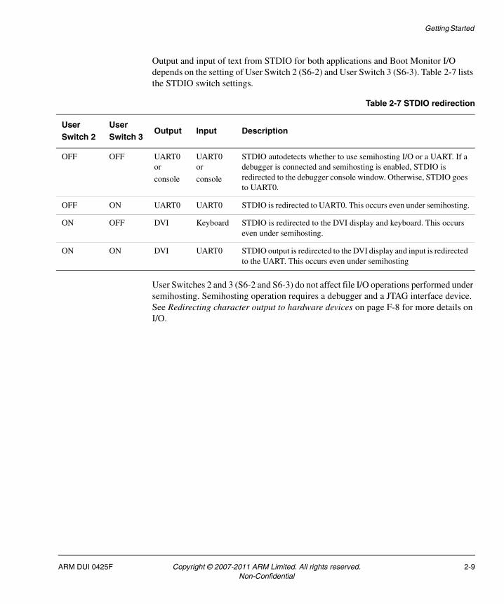
Getting Started
Output and input of text from STDIO for both applications and Boot Monitor I/O depends on the setting of User Switch 2 (S6-2) and User Switch 3 (S6-3). Table 2-7 lists the STDIO switch settings.
User Switches 2 and 3 (S6-2 and S6-3) do not affect file I/O operations performed under semihosting. Semihosting operation requires a debugger and a JTAG interface device. See Redirecting character output to hardware devices on page F-8 for more details on I/O.
Table 2-7 STDIO redirection
UserSwitch 2
UserSwitch 3
Output Input Description
OFF OFF UART0 or
console
UART0 or
console
STDIO autodetects whether to use semihosting I/O or a UART. If a debugger is connected and semihosting is enabled, STDIO is redirected to the debugger console window. Otherwise, STDIO goes to UART0.
OFF ON UART0 UART0 STDIO is redirected to UART0. This occurs even under semihosting.
ON OFF DVI Keyboard STDIO is redirected to the DVI display and keyboard. This occurs even under semihosting.
ON ON DVI UART0 STDIO output is redirected to the DVI display and input is redirected to the UART. This occurs even under semihosting
ARM DUI 0425F Copyright © 2007-2011 ARM Limited. All rights reserved. 2-9Non-Confidential

Getting Started
2.3 Connecting JTAG, Trace, and configuration equipment
You can use JTAG debugging equipment and the JTAG connector to:
• connect a debugger to the ARM1176JZF-S core and download programs to memory and debug them
• program new configuration images into the configuration flash, FPGA, and PLDs on the board. (You cannot program the normal flash from configuration mode.)
The JTAG connector is shown in Figure 2-2.
Figure 2-2 JTAG, Trace, and config connectors
Note The debug mode is selected by default and the JTAG port can be used to debug applications running on the processor.
If the CONFIG switch is ON, the JTAG or USB config port can be used to load FPGA images. For more details on JTAG debugging see JTAG debug port and USB config port support on page 3-51.
The following section describes:
• ARM CoreSight on page 2-11
• Connecting to the USB config port on page 2-13
• Connecting the Trace Port Analyzer on page 2-13.
Testchip
FPGA
JTAG
USB Config
Trace A
Trace B
2-10 Copyright © 2007-2011 ARM Limited. All rights reserved. ARM DUI 0425FNon-Confidential

Getting Started
2.3.1 ARM CoreSight
The ARM1176JZF-S development chip includes ARM CoreSight technology. See CoreSight Technology System Design Guide (DGI 0012) for background information on the CoreSight components and interconnect.
Trace capture
The main components used for trace capture are:
CoreSight ETM11, ETB, TPIU and DAP
• The CoreSight Embedded Trace Macrocell (ETM11) monitors the ARM core buses and outputs compressed information.
• The Embedded Trace Buffer (ETB), buffers the information using 8KB of on chip RAM.
• The Trace Port Interface Unit (TPIU) acts as a bridge between the on-chip trace data and the data stream that is captured by an external Trace Port Analyzer (TPA).
• The Debug Access Port (DAP) provides a dedicated JTAG Debug Port (JTAG-DP) for the debug tools and provides access to the CoreSight Debug APB through an APB-Mux. The ETM11, ETB and TPIU are configured and accessed over the Debug APB bus.
Trace connector and adaptor board
The trace connectors enable you to connect a TPA to the PB1176JZF-S. The connector is a high-density AMP Mictor connector. The pinout for these connectors is provided in Test and debug connections on page A-16.
The adaptor board buffers the high-speed signals between the Trace connectors and the Trace Port Analyzer.
Trace Port Analyzer
The TPA is an external device (such as RealView Trace) that connects to the trace connector (through the adaptor board) and stores information sent from the TPIU.
Debugger and Trace software
The debugger and trace software controls the JTAG unit, CoreSight ETM11, and TPA. The trace software reconstructs program flow from the information captured in the Trace Port Analyzer.
ARM DUI 0425F Copyright © 2007-2011 ARM Limited. All rights reserved. 2-11Non-Confidential

Getting Started
Note The trace and debug components must match the debugger you are using. ARM RealView Debugger (RVD) is a component of RealView Compilation Tools (RVCT) and supports RealView ICE and RealView Trace.
Always check with the manufacturer of the debug equipment what level of support is provided for CoreSight Technology.
System level debug
The CoreSight subsystem implemented in the ARM1176JZF-S development chip enables system level debug. The main CoreSight components are:
• ARM11 CoreSight Embedded Trace Macrocell (CoreSight ETM11)
• ARM11 Embedded Trace Buffer (ETB11) with 8KB memory
• Trace Port Interface Unit (TPIU)
• Debug Access Port (DAP)
• Cross Trigger Interfaces (CTI)
• Cross Trigger Matrix (CTM)
• Synchronous ATB Bridge.
The CoreSight subsystem enables real-time system level debug and trace of the ARM1176JZF-S development chip and external components. The internal AMBA Trace Bus (ATB) is accessible at the device pins through a Synchronous 1:1 ATB Bridge. On the PB1176JZF-S, the ATB connects to the tile site HDRZ connector. This enables CoreSight system debug to be extended to the tile site when this is supported by an attached tile and debug software.
Debug modes
For system level debug, fit jumper J1, (DAP ENABLE) on the PB1176JZF-S. This connects the DAP JTAG Debug Port (JTAG-DP) to the PB1176JZF-S JTAG debug scan-chain.
Note There is no JTAG connection to the CoreSight ETM11. Trace is only supported when using the DAP.
For legacy debug of the ARM1176JZF-S, remove jumper J1, (DAP ENABLE) on the PB1176JZF-S. This bypasses the DAP and connects the PB1176JZF-S JTAG debug scan-chain directly to the DBGTAP port on the ARM1176JZF-S.
2-12 Copyright © 2007-2011 ARM Limited. All rights reserved. ARM DUI 0425FNon-Confidential
Getting Started
2.3.2 Connecting to the USB config port
The USB config port on the PB1176JZF-S is shown in Figure 2-2 on page 2-10. Use a USB cable to connect the baseboard to a USB port on your workstation.
The USB config port does not connect to the onboard JTAG debug signals, but it does connect to the JTAG configuration signals and can be used to load new FPGA images.
Note • You must remove other JTAG devices, for example, the RVI from the JTAG
connector for the USB config port to work.
• You must set the CONFIG switch to ON to reprogram the FPGA images.
2.3.3 Connecting the Trace Port Analyzer
The ARM1176JZF-S development chip incorporates an ARM11 CoreSight Embedded Trace Macrocell (CoreSight ETM11). This enables you to carry out real-time debugging by connecting external trace equipment to the PB1176JZF-S. The ETM11 monitors the program execution and sends a compressed trace to the Trace Port Analyzer (TPA). The TPA buffers this information and transmits it to the debugger where it is decompressed and used to reconstruct the complete instruction flow. The trace size implemented by the Trace Port Interface Unit (TPIU) is large, (32-bit packets).
Note The ARM1176JZF-S development chip includes a Debug Access Port (DAP). When supported by CoreSight enabled hardware and software the DAP enables system-wide debug and trace.
Connect the Trace Port Analyzer (TPA) to the adaptor board and plug the adaptors into the PB1176JZF-S trace ports shown in Figure 2-2 on page 2-10. RealView Trace requires a RealView ICE JTAG unit. The Ethernet and power supply cables connect to the RealView ICE unit.
Note The high-density cable from the RealView ICE box requires a buffer board to connect to the JTAG connector on the PB1176JZF-S.
The low-density cable can be used to connect the RealView ICE box directly to the JTAG connector, but this interface operates at lower speed.
ARM DUI 0425F Copyright © 2007-2011 ARM Limited. All rights reserved. 2-13Non-Confidential

Getting Started
2.4 Supplying power
When using the PB1176JZF-S as a standalone development system, you must connect the supplied brick power supply to power socket J44 or an external bench power supply to the screw-terminal connector J46. See Figure 2-3.
Figure 2-3 Power connectors
Note If you are using the supplied brick power supply connected to J44, the Standby/power pushbutton S8 toggles the power on and off.
If you are using an external power supply connected to J46, or you are powering the board from the PCI backplane, the Standby/power switch is not used. You control the power by shutting down the external power source.
Caution You can use only one power source for the system. Use only the PCI connector, J46, or J44. Do not, for example, use the PCI connector and J46 at the same time.
Dev.Chip
FPGA
User push
buttons
PWR terminal
12V powerconnector
12V0V (GND)3V35V
3V3 OK LED
5V OK LED
Standby LED
Power switch
Force on link
Power link(paralled with power switch)
2-14 Copyright © 2007-2011 ARM Limited. All rights reserved. ARM DUI 0425FNon-Confidential

Chapter 3 Hardware Description
This chapter describes the on-board hardware. It contains the following sections:
• PB1176JZF-S architecture on page 3-2
• ARM1176JZF-S development chip on page 3-8
• Development chip peripherals on page 3-17
• FPGA peripherals on page 3-22
• FPGA configuration on page 3-30
• Reset controller on page 3-32
• Power supply on page 3-35
• Clock architecture on page 3-38
• Test, configuration, and debug interfaces on page 3-51.
ARM DUI 0425F Copyright © 2007-2011 ARM Limited. All rights reserved. 3-1Non-Confidential

Hardware Description
3.1 PB1176JZF-S architecture
The following sections describe the major architectural blocks in the PB1176JZF-S:
• PCB layout on page 3-3
• System architecture on page 3-4
• ARM1176JZF-S development chip on page 3-5
• PB1176JZF-S FPGA on page 3-5
• Displays on page 3-5
• RealView Logic Tile expansion on page 3-5
• Memory on page 3-6
• Clock generators on page 3-7
• Debug and test interfaces on page 3-7.
3-2 Copyright © 2007-2011 ARM Limited. All rights reserved. ARM DUI 0425FNon-Confidential

Hardware Description
3.1.1 PCB layout
Figure 3-1 shows the layout of the PB1176JZF-S.
Figure 3-1 PB1176JZF-S layout
Testchip
FPGA
12
34
56
78
ConfigurationDIP switches
GPIOJ39
PWR terminal
J46
12V power
J44
DVIJ21
KeyboardJ36
MouseJ35
User DIP switches
S6
User LEDs
Line in and out
J23Mic inJ24
MMC cardJ32
Mini SCIJ33
Logic Tile connectors
Memory expansion connector
J16
EthernetJ17 USB config
J15
JTAGJ12
User push button
Power button
SSP expansion
J31
PCI
Trace BJ3
Trace AJ2
OTG USBJ18
Dual USBJ19
Dual UARTJ26
Dual UARTJ27
UARTJ28
CODECJ25
1 21 2 3 4
S7 S1Character
LCD displayJ37
Reset
DC config
ILA interface
J11
FPGA BATT
SCI expansion
J29
J4
J5 J6
S3
S2
S4
S5
FPGA config
Configswitch
J41J40J42J43
UserReset
FPGA config
J47J45
DC config
Force onPower
Trace Tilestack J7
LEDD6
ARM DUI 0425F Copyright © 2007-2011 ARM Limited. All rights reserved. 3-3Non-Confidential
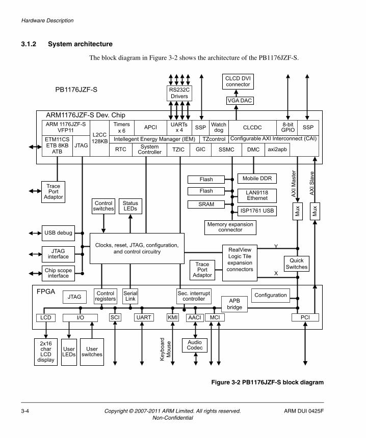
Hardware Description
3.1.2 System architecture
The block diagram in Figure 3-2 shows the architecture of the PB1176JZF-S.
Figure 3-2 PB1176JZF-S block diagram
Configurable AXI Interconnect (CAI)
MCIAACI
SSP
GIC
UARTsx 4
RTC
Timersx 6
User switches
Audio Codec
LAN9118 Ethernet
User LEDs
FPGA
ARM1176JZF-S Dev. Chip
TZcontrol
CLCD DVI connector
ISP1761 USB
2x16 char LCD
display
VGA DAC
KMI
SerialLink
Sec. interrupt controller
I/OLCD SCI PCIUART
Control registers
Clocks, reset, JTAG, configuration, and control circuitry
Mobile DDR
Flash
SRAM
Memory expansion connector
SSMC DMCTZIC axi2apb
CLCDC 8-bitGPIO SSPWatch
dogAPCI
System Controller
Trace Port
Adaptor
ARM 1176JZF-SVFP11
USB debug
JTAG interface
Chip scope interface
Status LEDs
Control switches
JTAG
ETM11CSETB 8KB
ATBJTAG
RealView Logic Tile expansion connectors
Flash
PB1176JZF-S
APB bridge
AX
I Mas
ter
AX
I Sla
ve
Configuration
Key
boar
dM
ouse
RS232CDrivers
L2CC128KB Intellegent Energy Manager (IEM)
Mux
Y
Mux
X
QuickSwitchesTrace
Port Adaptor
3-4 Copyright © 2007-2011 ARM Limited. All rights reserved. ARM DUI 0425FNon-Confidential

Hardware Description
3.1.3 ARM1176JZF-S development chip
For details on the ARM1176JZF-S development chip, see ARM1176JZF-S development chip on page 3-8.
3.1.4 PB1176JZF-S FPGA
The FPGA provides system control and configuration functions for the PB1176JZF-S that enable it to operate as a standalone development system or with expansion RealView Logic Tiles or as a PCI card. See FPGA configuration on page 3-30.
The FPGA also implements additional peripherals, for example audio CODEC and PCI interface.
3.1.5 Displays
The ARM1176JZF-S development chip outputs signals for a color LCD display.
The CLCD signals from the ARM1176JZF-S development chip are converted on the PB1176JZF-S to a VGA signal and a DVI signal and output to a DVI Digital/Analog connector. The resolution of the VGA signal is configurable. See ARM PrimeCell Color LCD Controller (PL111) Technical Reference Manual.
There is also a two row by sixteen character display mounted on the PB1176JZF-S. This display is accessed using a controller implemented in the FPGA and can be used for debugging or as the output from applications.
Note The memory controller bandwidth limits the resolution and color depth options, for example:
• 640 x 480 at 32-bit
• 800 x 600 at 16-bit.
3.1.6 RealView Logic Tile expansion
The ARM RealView Logic Tiles, such as the LT-XC2V6000, enable the development of AMBA 3 AXI peripherals, or custom logic, for use with the PB1176JZF-S.
You can place standard or custom peripherals in the FPGA on the RealView Logic Tile. Two multiplexed AXI buses are brought out to the RealView Logic Tile connectors HDRX and HDRY. See Appendix C RealView Logic Tile.
ARM DUI 0425F Copyright © 2007-2011 ARM Limited. All rights reserved. 3-5Non-Confidential

Hardware Description
Note The bus on the tile X header is the master interface and the bus on the tile Y header is the slave interface. If a Logic Tile is not fitted, quick switches on the PB1176JZF-S connect the PB1176JZF-S AXI master directly to the PB1176JZF-S slave interface.
3.1.7 Memory
The volatile memory includes SRAM and DDR memory:
• The development chip contains 512KB of on-chip SRAM. This memory can be partitioned using the development chip TrustZone protection controller into secure or non-secure blocks. The loading of secure memory can be performed through the debugger. The system is then reset to run from the secure memory.
• The PB1176JZF-S has 8MB of 32-bit asynchronous SRAM memory on board. This memory is controlled directly by the PL093 Synchronous Static Memory Controller in the ARM1176JZF-S development chip and can be secured by the TrustZone Protection Controller (TZPC).
• You can expand the SRAM memory by installing an external PISMO static memory expansion board. See Appendix E Memory Expansion Boards.
• The PB1176JZF-S has 128MB of 32-bit Mobile DDR memory on board. This memory is controlled directly by the PL340 Dynamic Memory Controller in the ARM1176JZF-S development chip.
Note So that the Dynamic Memory interface can be operated at high frequency without
any potential signal integrity or timing problems, no provision is made for expansion of the SDRAM memory.
The nonvolatile memory system consists of:
• Two banks of 64MB 32-bit NOR flash.
• The development chip contains 16KB of on-chip SRAM that can be configured as a pseudo-ROM that can selected as boot memory. It is not actually nonvolatile because the contents do not survive power cycling, but the contents do remain valid after reset.
• There is also 16MB of flash memory dedicated to holding the FPGA image. You must not program this flash memory in user mode because it contains FPGA configuration.
3-6 Copyright © 2007-2011 ARM Limited. All rights reserved. ARM DUI 0425FNon-Confidential

Hardware Description
The NOR flash memory is managed by the PL093 Synchronous Static Memory Controller in the ARM1176JZF-S development chip.
3.1.8 Clock generators
The PB1176JZF-S has the following clock sources:
• 24MHz Reference clock for configuration and PLLs.
• Five ICS307 programmable clock generators. These clocks are connected to the system FPGA. System control registers in the FPGA translate the clock settings to a serial stream that is output to the clock generators to select the clock division ratios.
• 32,768Hz Reference Clock for RTC.
• If fitted, clocks from the PCI backplane, RealView Logic Tiles or Core Tiles can be selected as the reference clocks for the PB1176JZF-S.
See Clock architecture on page 3-38.
3.1.9 Debug and test interfaces
The JTAG connector enables JTAG hardware debugging equipment, such as RealView ICE®, to be connected to the PB1176JZF-S. See JTAG debug port and USB config port support on page 3-51. (The JTAG config chain signals can also be controlled by the on-board USB config port controller and used to load FPGA images.)
Two Mictor connectors on the PB1176JZF-S enable monitoring of the ARM1176JZF-S development chip Embedded Trace Macrocell® (ETM11) signals by a Trace Port Analyzer (TPA). The trace port supports a trace packet size of 16-bit (medium) and 32-bit (large). See Trace connector pinout on page A-18 for connection information.
A single trace port connector is also provided for some of the Logic Tile HDRY signals. See also Table C-4 on page C-14.
ARM DUI 0425F Copyright © 2007-2011 ARM Limited. All rights reserved. 3-7Non-Confidential

Hardware Description
3.2 ARM1176JZF-S development chip
The ARM1176JZF-S development chip and its interfaces are described in the following sections:
• ARM1176JZF-S development chip overview on page 3-9
• Configuration control on page 3-13
• AXI buses on page 3-14
• Intelligent Energy Management on page 3-15.
For more information on using the ARM1176JZF-S development chip components, see also:
• Development chip peripherals on page 3-17
• ARM1176JZF-S development chip clocks on page 3-40
• Reset controller on page 3-32
• Chapter 4 Programmer’s Reference.
3-8 Copyright © 2007-2011 ARM Limited. All rights reserved. ARM DUI 0425FNon-Confidential

Hardware Description
3.2.1 ARM1176JZF-S development chip overview
Figure 3-3 shows the main blocks of the ARM1176JZF-S development chip.
Figure 3-3 ARM1176JZF-S development chip block diagram
ARM1176JZF-S Dev. Chip
GIC
CLCDC (PL110)
DMC(PL340)
IEM
VFP11
SSMC(PL093)
CoreSightETM11, DAP
AX
I2A
PB
Con
figur
able
AX
I Int
erco
nnec
t (P
L300
)
TrustZoneinterrupt controller
JTAG
IEC(SY750)
TZPC(BP147)
System Controller
RTC (PL031)
UART x4 (PL011)
Watchdog (SP805)
SSP1 (PL022)
GPIO (PL061)
Dual Timer (SP804) x3
32KB I cache32KB D cache
ARM1176JZFcore
AXI master port
AXI slave port
ATB
Configuration,reset, PLL ratio and clock select
8KB I TCM8KB D TCM
16KB boot RAM
128KB unified cache
512KB RAM
L2CC
ARM DUI 0425F Copyright © 2007-2011 ARM Limited. All rights reserved. 3-9Non-Confidential

Hardware Description
The ARM1176JZF-S development chip incorporates the following features:
ARM1176JZF-S
The ARM1176JZF-S CPU is a member of the ARM11 Thumb® family. The ARM1176JZF-S macrocell is a 32-bit cached processor with ARM architecture v6 that supports the ARM and Thumb instruction sets and includes features for direct execution of Java byte codes. Executing Java byte codes requires the Java Technology Enabling Kit (JTEK). The development chip also contains:
Cache Cache memory for instruction (32KB) and data (32KB).
Level 2 Cache Controller (L2CC) with 128KB unified cache.
DSP A range of Single Instruction Multiple Data (SIMD) DSP instructions that operate on 16-bit or 8-bit data values in 32-bit registers
MMU The ARM1176JF-S contains a Memory Management Unit (MMU).
TCM 8KB of data and instruction Tightly Coupled Memory (TCM). The TCM operates with a single wait-state and provides higher data rates than external memory.
VFP Vector Floating Point coprocessor (VFP), supporting the ARM VFPv2 floating point coprocessor instruction set.
TrustZone TrustZone security extensions:
• TrustZone Interrupt Controller (TZIC)
• TrustZone Protection Controller (TZPC).
IEM Provision for Intelligent Energy Management (IEM):
• ARM Intelligent Energy Controller (IEC)
• National Semiconductor Advanced Power Controller (APCI)
• National Semiconductor Hardware Performance Monitor (HPM).
AXI RAM AXI RAM (512KB) and boot ROM emulation (16KB).
AXI buses The ARM1176JF processor uses the Configurable AXI Interconnect to connect the processor core to the on-chip AXI controllers and peripherals. An AXI to APB bridge provides the interface to the APB-based peripherals in the development chip.
One external AXI master bus and one external AXI slave bus provide the interface to the FPGA peripherals and the optional Logic Tile.
CAI Configurable AXI Interconnect (CAI).
3-10 Copyright © 2007-2011 ARM Limited. All rights reserved. ARM DUI 0425FNon-Confidential

Hardware Description
CoreSight CoreSight components include:
• CoreSight Embedded Trace Module (ETM11)
The Embedded Trace Macrocell (ETM) provides signals for off-chip trace. The ETM transmits a 16-bit packet to an external trace port analyzer where the signals can be stored and later analyzed to reconstruct the code flow.
• CoreSight Embedded Trace Buffer (ETB11), 8KB memory.
VFP11 This high-performance, low-power Vector Floating-Point (VFP) coprocessor implements the VFPv2 vector floating-point architecture.
Clock control
The ARM1176JZF-S development chip contains deskew PLLs that use an external reference clock to generate internal clocks for the CPU, AHB bus, memory, and off-chip peripherals. Dividers in the chip are programmable and give flexibility in setting clock rates for the CPU, bridges, and memory.
Memory controllers
The ARM1176JZF-S development chip includes an AXI memory controller (for dynamic memory) and a single port static memory controller AHB device. Both controllers have 32-bit interfaces to external memory. See Memory interface on page 3-17.
Interrupt controller
The PrimeCell GIC provides an interface to the interrupt system and provides vectored interrupt support for high-priority interrupt sources from:
• peripherals in the ARM1176JZF-S development chip
• peripherals in the FPGA (a secondary interrupt controller is present in the FPGA). These are routed through the TZIC in the development chip.
See Interrupt controllers on page 3-19.
CLCD controller
The CLCDC provides a flexible display interface that supports a VGA monitor and digital LCD displays (external interface circuitry connects the CLCD output to a DVI Digital/Analog connector on the board). See CLCDC interface on page 3-18.
ARM DUI 0425F Copyright © 2007-2011 ARM Limited. All rights reserved. 3-11Non-Confidential

Hardware Description
UART The four UARTs perform serial-to-parallel conversion on data received from a peripheral device and parallel-to-serial conversion on data transmitted to the peripheral device. (An additional UART is provided by the FPGA.) See UART interface on page 3-20.
Timers There are six 32-bit down counters that can be used to generate interrupts at programmable intervals. A Real-Time-Clock is fed with an external 1Hz signal.
Synchronous serial port
The SSP provides a master or slave interface for synchronous serial communications using Motorola SPI, TI, or National Semiconductor Microwire devices.
Smart Card interface
The Smart Card interface signals are programmable to enable support for a Smart Card, Security Identity Module (SIM) card, or similar module.
GPIO Eight bits of GPIO are provided by the on-chip interface. (An additional GPIO is provided by the FPGA.)
Watchdog A Watchdog module can be used to trigger an interrupt or system reset in the event of software failure.
3-12 Copyright © 2007-2011 ARM Limited. All rights reserved. ARM DUI 0425FNon-Confidential

Hardware Description
3.2.2 Configuration control
The PB1176JZF-S uses configuration switches and the SYS_CFGDATAx registers in the FPGA to control configuration of the ARM1176JZF-S development chip at power-up.
After reset, configuration can be modified by the system controller and the configuration registers in the FPGA. For example, you can simulate a system that boots with the vector table located at address 0xFFFF0000 by changing the value of bits 0 and 1 in the SYS_CFGDATA2 register and pressing the DC RECONFIG button.
See FPGA status and system control registers on page 4-37 and Configuration registers SYS_CFGDATAx on page 4-45.
Configuration switches
The S1 switches select boot memory and the startup clock frequency. For more information on setting boot memory options, see Setting the configuration switches on page 2-3 and Memory map on page 4-3.
Changing the ARM1176JZF-S development chip configuration at runtime
The ARM1176JZF-S development chip has many configuration options (clock selection for example) that are configured by loading configuration values onto the data bus when a chip reconfigure signal is received.
To change the configuration of the ARM1176JZF-S development chip:
1. Program the appropriate values in the SYS_CFGDATAx registers, see Configuration registers SYS_CFGDATAx on page 4-45.
2. Perform a configuration reset of the PB1176JZF-S, but do not power-cycle, by either:
• pressing the DEV CHIP RECONFIG pushbutton (next to the blue LED)
• programming the reset-depth register to level 2 (see Reset Control Register, SYS_RESETCTL on page 4-49) and then performing a normal reset from software, the reset pushbutton, or JTAG.
Restoring the default configuration
To restore the default processor configuration, power-cycle the PB1176JZF-S or press the FPGA CONFIG pushbutton.
ARM DUI 0425F Copyright © 2007-2011 ARM Limited. All rights reserved. 3-13Non-Confidential
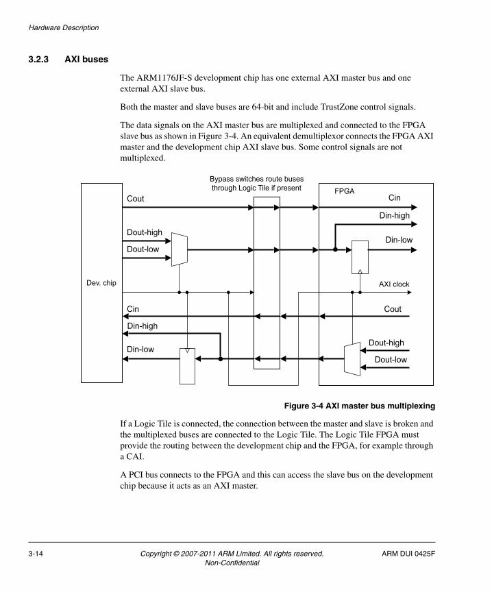
Hardware Description
3.2.3 AXI buses
The ARM1176JF-S development chip has one external AXI master bus and one external AXI slave bus.
Both the master and slave buses are 64-bit and include TrustZone control signals.
The data signals on the AXI master bus are multiplexed and connected to the FPGA slave bus as shown in Figure 3-4. An equivalent demultiplexor connects the FPGA AXI master and the development chip AXI slave bus. Some control signals are not multiplexed.
Figure 3-4 AXI master bus multiplexing
If a Logic Tile is connected, the connection between the master and slave is broken and the multiplexed buses are connected to the Logic Tile. The Logic Tile FPGA must provide the routing between the development chip and the FPGA, for example through a CAI.
A PCI bus connects to the FPGA and this can access the slave bus on the development chip because it acts as an AXI master.
Dev. chip
Dout-high
Dout-low
Din-high
Din-low
Cin
Cout
Dout-high
Dout-low
Din-high
Din-low
Cin
Cout
FPGABypass switches route buses through Logic Tile if present
AXI clock
3-14 Copyright © 2007-2011 ARM Limited. All rights reserved. ARM DUI 0425FNon-Confidential

Hardware Description
3.2.4 Intelligent Energy Management
Note The Intelligent Energy Management (IEM) subsystem uses an Advanced Power Controller (APC) provided by a third-party. The APC requires a separate license for the controller and the documentation on the controller registers.
Contact ARM for more information on licensing the APC component and obtaining the documentation required to use the APC with the IEM subsystem.
The development chip has several mechanisms for reducing system power usage:
• reducing the core and RAM supply voltages
• turing off sections of the core that are not used
• changing the operating frequency of the core.
The IEM performance level and PLL controller is responsible for:
• receiving performance requests from the IEC
• sending and monitoring performance requests to the APC and DCG
• configuring the PLLs
• instructing the clock selection block to select a PLL.
The IEM subsystem consists of the:
• Intelligent Energy Controller (IEC)
• Dynamic Clock Generator (DCG)
• System controller
• Dynamic Voltage Controller (DVC).
The IEM block also controls the safe entry and exit from low power modes including StandbyWFI, shutdown and dormant modes. The IEM PLL controller consists of the performance level controller state machine and PLL configuration select blocks (see also Development chip Dynamic Clock Generator on page 3-47).
User software running on the ARM1176JZF core, requests the required performance level through the IEC. The IEC communicates with the DCG and DVC to provide the required combination of voltage and clock frequency to satisfy the performance requirements. The IEC, system controller, and DVC, are all APB memory-mapped peripherals.
See also DCG Fractional Performance Level Mapping Registers on page 4-18, Processor Frequency Configuration Register on page 4-18 and Advanced Power Controller and Power Management Interface on page 4-22.
ARM DUI 0425F Copyright © 2007-2011 ARM Limited. All rights reserved. 3-15Non-Confidential

Hardware Description
Run mode
This is the normal mode after reset. IEM software only operates in this mode.
The Run Mode Performance Level Controller State Machine receives performance level requests from the IEC and ensures safe movement between performance levels. A state machine ensures that when moving between performance levels, the required PLL has locked, and the IEM subsystem voltage level is adequate.
This state machine controls IEM through all active performance levels. If 0% performance is selected, the system either enters StandbyWFI, Shutdown or Dormant mode depending on system settings.
StandbyWFI mode
StandbyWFI mode is entered whenever the IEC selects 0% performance, and neither SHUTDOWNNXT nor DORMANTNXT flags are set. When entering StandbyWFI mode, no new voltage requests are made to the APC. Voltage is therefore held at the current level prior to requesting 0% performance. For closed loop, the clock to the HPM is not interrupted and closed loop voltage control continues to operate as normal.
Dormant and shutdown modes
In shutdown mode, the whole IEM subsystem is powered down. This includes the ARM1176JZF, L2CC, and ETM11. Shutdown and dormant modes are controlled by setting the SHUTDOWNNXT or DORMANTNXT flag in the system controller.
IEM subsystem permanent shutdown mode
An external master can have full control of the chip because the configuration option is available to completely disable the IEM subsystem. This includes the ARM1176JZF, CoreSight ETM11, and L2CC. Enable permanent IEM subsystem shutdown by setting CFGIEMSHUTDOWN bit (see Table 4-37 on page 4-45). If permanent shutdown is selected, the IEM subsystem is held in reset and input and output clamps are enabled. You can therefore safely power-down the IEM subsystem.
3-16 Copyright © 2007-2011 ARM Limited. All rights reserved. ARM DUI 0425FNon-Confidential

Hardware Description
3.3 Development chip peripherals
This section describes peripherals and controllers located in the development chip. It contains the following sections:
• Memory interface
• CLCDC interface on page 3-18
• GPIO interface on page 3-18
• Interrupt controllers on page 3-19
• Synchronous Serial Port, SSP on page 3-19
• UART interface on page 3-20.
3.3.1 Memory interface
Memory access is provided by a Dynamic Memory Controller (DMC) and a Synchronous Static Memory Controller (SSMC) located in the ARM1176JZF-S development chip. One or more static expansion memory boards can be connected to the memory expansion connector.
Memory (or memory-mapped peripherals) can also be accessed on an optional Logic Tile or PCI card.
Note The memory at 0x00000000 and 0x3C000000 at boot time is determined by the boot select switches and the remap signals (see Memory aliasing at reset on page 3-33).
The region at 0x80000000–0xFFFFFFFF is recommended for accesses to a Logic Tile.
PCI cards must be initialized before use (see PCI configuration on page 4-115).
ARM DUI 0425F Copyright © 2007-2011 ARM Limited. All rights reserved. 3-17Non-Confidential

Hardware Description
Figure 3-5 Memory devices
3.3.2 CLCDC interface
A PrimeCell Color LCD controller (CLCDC) is present in the ARM1176JZF-S development chip.
The PB1176JZF-S provides a display interface with outputs to a DVI Digital/Analog connector for connecting to a CLCD monitor
A DAC converts the rearranged CLCD signals into VGA analog signals.
See Color LCD Controller, CLCDC on page 4-32 for interface details.
3.3.3 GPIO interface
The GPIO signals GPx_[7:0] from the ARM1176JZF-S development chip are connected to the GPIO connectors.
128MBMobile DDR
0x00000000-0x07FFFFFF
Dynamic memory address, data, and control signals
64MB NOR flashCS7
0x3C000000-0x3FFFFFFF
8MB Cellular RAM
CS5
0x34000000-0x37FFFFFF
Staticexpansion
socketCS[0:3]
0x20000000-0x2FFFFFFF
64MB Secure NOR flash
CS4
0x30000000-0x33FFFFFF
Chip select, multiplex, and decode logic
Bootselect switches
ARM1176JZF Dev. Chip
SMC (PL093)
DMC (PL340)
Static memory address, data and control signals
Memory or memory-mapped peripherals on PCI cards
0x60000000-0x6FFFFFFF
AXI master
Memory or memory-mapped peripherals on customized
RealView Logic Tiles
0x80000000-0xFFFFFFFF
EthernetandUSB
0x3A000000-0x3BFFFFFF
3-18 Copyright © 2007-2011 ARM Limited. All rights reserved. ARM DUI 0425FNon-Confidential

Hardware Description
See also General Purpose Input/Output, GPIO on page 4-57 and the ARM PrimeCell GPIO (PL061) Technical Reference Manual. See GPIO interface on page A-12 for connector pinout information.
3.3.4 Interrupt controllers
The ARM1176JZF-S development chip contains a Generic Interrupt Controller (GIC) and a TrustZone Interrupt Controller (TZIC). Two additional GICs are in the FPGA. Figure 3-6 shows the interconnections between the peripherals and the interrupt controllers.
Figure 3-6 Interrupt controller block diagram
For details on the programming model for the interrupt controllers, see Interrupt controllers in the ARM1176JZF-S development chip on page 4-58.
3.3.5 Synchronous Serial Port, SSP
The ARM1176JZF-S development chip contains a PrimeCell SSP controller. Use expansion connector J31 to connect to the SSP. The FPGA controls the SSP peripheral chip select.
ARM1176JF-S development chip
PISMO
Ethernet
USB
PCI bus
FPGA peripherals Dev. chip
peripherals(23 interrupts)
Logic Tile HDRZ
FPGA
TZICARM1176JZF-S
IRQINT[31:0]
nIRQ
nFIQ
nIRQnFIQ
GIC
GIC1GIC0
Inactive (reserved)
Interrupts from tile site
ARM DUI 0425F Copyright © 2007-2011 ARM Limited. All rights reserved. 3-19Non-Confidential
Hardware Description
The SSP functions as a master or slave interface that enables synchronous serial communication with slave or master peripherals having one of the following:
• a Motorola SPI-compatible interface
• a Texas Instruments synchronous serial interface
• a National Semiconductor Microwire interface.
See also Synchronous Serial Port, SSP on page 4-124 and the ARM PrimeCell Synchronous Serial Port Controller (PL022) Technical Reference Manual.
3.3.6 UART interface
Four UARTs (SER0, SER1, SER2, and SER3) are provided by the ARM1176JZF-S development chip.
A fifth UART, SER4, is implemented with a PrimeCell UART incorporated in the FPGA.
The UARTs have the following features:
• functionally similar to standard 16C550 devices
• port function corresponds to the DTE configuration
• SER0 and SER4 (UART0 and UART4) have full CTS, RTS, DCD, DSR, DTR, and RI modem control signals
• SER1, SER2, and SER3 (UART1, UART2, and UART3) have simple modem control signals CTS and RTS
• programmable baud rates of up to 1.5Mbits per second (the line drivers however, are only guaranteed to 250kbps)
• 16-byte transmit FIFO
• 16-byte receive FIFO
• programmable interrupt.
The signals from the ARM1176JZF-S development chip UARTs and the FPGA UART are converted from logic level to RS232 level by MAX3243E buffers.
See also UART on page 4-140 and the ARM PrimeCell UART (PL011) Technical Reference Manual.
3-20 Copyright © 2007-2011 ARM Limited. All rights reserved. ARM DUI 0425FNon-Confidential
Hardware Description
The signals associated with the UART interface are shown in Table 3-1.
Table 3-1 Serial interface signal assignment
Signal Description
SERx_TXD Transmit data
SERx_RTS Ready to send
SERx_DTRa
a. For UART1, UART2, and UART3, the DTR and DSR signals are connected together and are not input to the ARM1176JZF-S development chip or FPGA.
Data terminal ready
SERx_CTS Clear to send
SERx_DSRa Data set ready
SERx_DCDb
b. For UART1, UART2, and UART3, the DCD and RI signals are not connected to the ARM1176JZF-S development chip or FPGA.
Data carrier detect
SERx_RXD Receive data
SERx_RIb Ring indicator
ARM DUI 0425F Copyright © 2007-2011 ARM Limited. All rights reserved. 3-21Non-Confidential

Hardware Description
3.4 FPGA peripherals
This section describes the peripherals present in the FPGA. It contains the following sections:
• FPGA architecture on page 3-23
• Character LCD controller on page 3-24
• Advanced Audio Codec Interface, AACI on page 3-24
• Keyboard/Mouse Interface, KMI on page 3-24
• Memory Card Interface, MCI on page 3-25
• Smart Card interface, SCI on page 3-25
• Serial bus interface on page 3-26
• User switches and LEDs on page 3-26
• USB interface on page 3-27
• PCI interface on page 3-27
• Ethernet interface on page 3-29.
3-22 Copyright © 2007-2011 ARM Limited. All rights reserved. ARM DUI 0425FNon-Confidential

Hardware Description
3.4.1 FPGA architecture
Figure 3-7 shows the architecture of the FPGA on the PB1176JZF-S.
Figure 3-7 FPGA block diagram
MCI
AACI interface
UART4
AXI/APB bridge
System registers
Smart card interface
Ethernet interface
PCI interface
Char LCD interface
Switch and LED
FPGA
AXI M
ARM1176JZF Dev. Chip
Serial bus interface
AXI S
PCI edge connector
LM549BAC97 CODEC
16x2Character LCD
display
JTAG
Config PLD and flash
Con
figur
atio
n lo
gic
Programmable clock
generators
2 x KMI
Reset and configuration
signals
GIC TZIC
Secondary GICs
USB interface
GPIO
PCICTRL
RTC
PWRMGR
DAP ROM
APB GIC
SYSCTRL
CAIAXI matrix
Downsize
SBCon
TZPC
ARM DUI 0425F Copyright © 2007-2011 ARM Limited. All rights reserved. 3-23Non-Confidential
Hardware Description
3.4.2 Character LCD controller
The FPGA contains a simple controller that provides an interface to a standard HD44780 16 x 2 character LCD alphanumeric display module. See Character LCD display on page 4-29 for details of the control registers for the display.
The character display has an 8-bit interface.
LK10 is installed at the factory to match the voltage requirement of the particular display module installed on the board.
3.4.3 Advanced Audio Codec Interface, AACI
The FPGA contains an ARM PrimeCell Advanced Audio CODEC Interface (AACI) that provides communication with a CODEC using the AC-link protocol. This section provides a brief overview of the AACI. For detailed information, see PrimeCell Advanced Audio CODEC Interface (PL041) Technical Reference Manual.
Note For a description of the audio CODEC signals, see the LM4549 datasheet available from the National Semiconductor website. See also Advanced Audio CODEC Interface, AACI on page 4-27.
The AACI on the PB1176JZF-S connects to a National Semiconductor LM4549 audio CODEC that is compatible with AC’97 Rev 2.1.
Two microphone inputs are present on J4. Only monophonic sound is supported, but microphone channel CODEC_MIC1 or CODEC_MIC2 can be selected in software. Solder link LK1 selects passive or active (electret) microphones:
Link AB Active microphone with power on CODEC_MIC1 (tip). Passive microphone on CODEC_MIC2 (not powered).
This is the default configuration.
Link BC Active microphone with power on CODEC_MIC2 (ring). Passive microphone on CODEC_MIC1 (not powered).
No link Passive microphone on CODEC_MIC1 and CODEC_MIC2.
3.4.4 Keyboard/Mouse Interface, KMI
The Keyboard and Mouse Interfaces (KMI) are implemented with two PrimeCells incorporated into the FPGA.
See also Keyboard and Mouse Interface, KMI on page 4-107 and the ARM PrimeCell PS2 Keyboard Mouse Controller (PL050) Technical Reference Manual.
3-24 Copyright © 2007-2011 ARM Limited. All rights reserved. ARM DUI 0425FNon-Confidential

Hardware Description
3.4.5 Memory Card Interface, MCI
The ARM PrimeCell Multimedia Card Interface (MCI) PL180 is an Advanced Microcontroller Bus Architecture (AMBA) slave block that connects to the Advanced Peripheral Bus (APB).
The PrimeCell MCI provides all functions specific to the multimedia and secure digital memory card such as the clock generation unit, power management control, and command a data transfer. The interface conforms to Multimedia Card Specification v2.11 and Secure Digital Memory Card Physical Layer Specification v0.96.
See MultiMedia Card Interfaces, MCI on page 4-108 and the ARM PrimeCell Multimedia Card Interface (PL180) Technical Reference Manual (ARM DDI 0172) for full programming details.
The signals on the PB1176JZF-S connector are shown in MMC and SD flash card interface on page A-9.
3.4.6 Smart Card interface, SCI
The ARM PrimeCell Smart Card Interface (SCI) PL131 is an Advanced Microcontroller Bus Architecture (AMBA) slave block that connects to the Advanced Peripheral Bus (APB).
The PrimeCell Smart Card Interface (SCI) interfaces to an external Smart Card reader. The SCI can autonomously control data transfer to and from the smart card. Transmit and receive data FIFOs are provided to reduce the required interaction between the host system and the peripheral.
You can set the Smart Card interface voltage to operate at 5V, 3.3V or 1.8V by setting jumpers on J34:
• Connect pins AB for 3.3V operation
• Connect pins CB for 5V operation
• omit the link for 1.8V operation.
The default setting is linking pins AB. Both 3.3V and 5V cards function with this setting.
Note The Smart Card VCC is switched on and off by the SCIVCCENx signal from the PrimeCell.
ARM DUI 0425F Copyright © 2007-2011 ARM Limited. All rights reserved. 3-25Non-Confidential

Hardware Description
See also Smart Card Interface, SCI on page 4-123, the SCI PrimeCell PL131 Technical Reference Manual. The signals on the Smart Card connector and expansion connector are described in Smart Card interface on page A-3.
3.4.7 Serial bus interface
The FPGA implements a serial bus interface that identifies the memory expansion modules, read and set the time-of-year clock, and identify displays connected to the DVI Digital/Analog connector.
Each device on the serial bus has its own slave address. The unique address for each slave on the serial bus is shown in Table 3-2.
3.4.8 User switches and LEDs
The FPGA provides a switch and LED register that enables you to read the general-purpose pushbutton switch and the user switches (S6) and light the user LEDs (located next to switch S6). See Figure 2-1 on page 2-3 for the location of the switches and LEDs.
Note The Boot Monitor reads switches S6-1 and S6-3 to determine start-up settings after reset. See Boot Monitor configuration on page 2-8.
Set bits [7:0] in the SYS_LED register at 0x10000008 to illuminate LEDs 7–0. The state of the user switches S6[8:1] is present on bits [7:0] of the SYS_SW register at 0x10000004.
Table 3-2 Serial interface device addresses
DeviceWrite address
Read address
Description
PISMO (static memory module)
0xA2 0xA3 Identifies the type of memory on the board and how it is configured.
TOY (DS1338 RTC) 0xD0 0xD1 Reads time data and writes control data to the RTC.
DVI Digital/Analog (external display)
display dependant
display dependant
Reads the capabilities of the external display connected to the DVI Digital/Analog connector. Can control display settings of E-DDC displays.
3-26 Copyright © 2007-2011 ARM Limited. All rights reserved. ARM DUI 0425FNon-Confidential
Hardware Description
The state of the general-purpose pushbutton S3 can be read from bit 4 of the SYS_MISC register at 0x10000060. Setting bit 3 of SYS_MISC causes a S3 depression to generate a PWRFAIL interrupt. The interrupt can be used to test auto-shutdown code or to awaken the processor from sleep mode. See Miscellaneous System Control Register, SYS_MISC on page 4-52.
3.4.9 USB interface
The FPGA provides the bus interface to an external ISP1761 USB controller. Three USB interfaces are provided on the PB1176JZF-S:
• ISP1761 USB port 1 provides an OTG device interface and connects to J18.
• ISP1761 USB ports 2 and 3 can function in either master or slave mode and connect to the dual type A connector J19 (USB2 is the top connector).
The signals on the USB interfaces are listed in USB interface on page A-6.
Note For a full description of the USB controller, see the datasheet for the NXP ISP1761. See USB interface on page 4-142 for details of the control register addresses.
Note The USB Debug interface has a dedicated USB controller and connects to the USB B-Type connector. It is only used for downloading new FPGA images and is not accessible from software running in the development chip.
3.4.10 PCI interface
The PCI subsystem enables you to use PCI expansion cards with the PB1176JZF-S when plugged into the PCI enclosure, or plug into a PC as a card.
PCI bridges pass valid accesses between the PB1176JZF-S and the PCI bus.
The slave bridge connected to the AHB M2 bus recognizes addresses 0x46000000 to 0x6FFFFFFF as being intended for a target within the PCI address space of the memory map, and passes accesses within this region to the PCI bus. The PCI_IMAPx registers define the address translation values for the PCI I/O, PCI configuration, and PCI memory windows.
The PCI_SMAPx registers define the address translation values for PCI accesses to the AHB S bus.
ARM DUI 0425F Copyright © 2007-2011 ARM Limited. All rights reserved. 3-27Non-Confidential

Hardware Description
The AHB to PCI bridge supports read and write accesses in both directions, as shown in Figure 3-8.
Figure 3-8 PCI bridge
See also and Appendix D PCI Backplane and Enclosure and PCI controller on page 4-109.
Arbiter
PCI Backplane
OutboundFIFO
Addresstransactionwindows
SlaveAXI
PCI_IMAPxregisters
PCI_SMAPxregisters
Addresstranslation windows
InboundFIFO
MasterAXI
AXImaster
AXIslave
CAI AXI matrix
PB1176JZF-S FPGA
AXI MuxAXI DeMux
AXI DeMux
AXI Mux
ARM1176JZF-S Development Chip
Slot 1Slot 2
Slot 3
Xilinx PCI to AMBA bridge
3-28 Copyright © 2007-2011 ARM Limited. All rights reserved. ARM DUI 0425FNon-Confidential
Hardware Description
3.4.11 Ethernet interface
The Ethernet interface is implemented with a SMC LAN9118 10/100 Ethernet single-chip MAC and PHY. The device is attached to the static memory bus from the development chip.
The isolating RJ45 connector incorporates two network status LEDs. The function of the LEDs can be set to indicate link, activity, transmit, receive, full duplex, or 10/100 selection. See the data sheet for the LAN9118 for more details on programming the registers.
The SMCS LAN9118 is a fast Ethernet controller that incorporates a Media ACcess (MAC) Layer, a PHYsical (PHY) layer, and an 8KB dynamically configurable transmit and receive FIFO.
The controller supports dual-speed 100Mbps or 10Mbps and auto configuration. When auto configuration is enabled, the chip is automatically configured for network speed and for full or half-duplex operation.
The controller connects to the ARM1176JZF-S development chip SMC using CS6, which is shared with the USB port.
The LAN9118 is a little-endian device. The default configuration for the system bus is also little-endian.
A serial EEPROM provides the following parameters to the LAN9118 at reset:
• the individual MAC address, that is, the Ethernet MAC address
• Media Independent Interface (MII) interface configuration
• register base address.
When the PB1176JZF-S is manufactured, an ARM value for the Ethernet MAC address and the register base address are loaded into the EEPROM. A unique MAC address is programmed at manufacture, but the address can be reprogrammed if required. Reprogramming of the EEPROM is done through LAN9118 Bank 1 (general and control registers).
ARM DUI 0425F Copyright © 2007-2011 ARM Limited. All rights reserved. 3-29Non-Confidential

Hardware Description
3.5 FPGA configuration
This section describes how the FPGA image is selected and loaded.
Caution The 1.5V cell battery provides the VBATT backup voltage to the external DS1338 time-of-year clock and FPGA encryption key circuitry within the FPGA. Removing the battery erases the encryption key.
Each board is provided with an encryption key that is unique to the board. The standard image supplied with the board is not encrypted. However, encrypted images might be supplied by ARM in the future. If you are using encrypted images and the key is erased, you must return the board to ARM to have the key reloaded.
The battery is expected to last for approximately 10 years from manufacture of the PB1176JZF-S. To replace the battery:
1. Power on the PB1176JZF-S. If the battery is removed while the board is powered down, the encryption key is erased.
2. Remove the old battery.
3. Insert the new battery and ensure that the positive terminal is facing upwards in the holder.
For details on FPGA components, see FPGA peripherals on page 3-22.
Note The ARM1176JZF-S development chip and FPGA AXI buses on the PB1176JZF-S are shared with the Logic Tile headers. If you are using a Logic Tile, ensure that the tile manages the bus signals correctly.
3-30 Copyright © 2007-2011 ARM Limited. All rights reserved. ARM DUI 0425FNon-Confidential

Hardware Description
At power-up the FPGA loads its configuration data from a flash memory device. Parallel data from the flash memory is streamed by the configuration PLD into the configuration ports of the FPGA.
The image loaded into the FPGA is determined by configuration switches S1-6 and S1-7 as described in FPGA image selection on page 2-5.
Note The configuration flash can hold four FPGA images. However, only one FPGA image is provided.
The configuration flash is a separate device and not part of the user flash.
You can use a JTAG debugger or the USB config port and the Progcards utility to reprogram the PLDs, FPGA, and flash if the PB1176JZF-S is placed in configuration mode.
See Appendix H Loading FPGA Images and JTAG debug port and USB config port support on page 3-51. The PB1176JZF-S is supplied with the configuration PLD and flash image already programmed. The information in the section is provided, however, in case of accidental erasure of the configuration PLD or flash image.
ARM DUI 0425F Copyright © 2007-2011 ARM Limited. All rights reserved. 3-31Non-Confidential

Hardware Description
3.6 Reset controller
The reset controller initializes the ARM1176JZF-S development chip, the FPGA, and external controllers as a result of a reset. The PB1176JZF-S can be reset from the following sources:
• power failure
• reset button
• PCI backplane
• Logic Tiles
• JTAG
• software.
Note Use the RESET pushbutton (nPBRESET), the JTAG reset signal (nSRST), the PCI backplane reset signal (P_nRST), the Logic Tile reset signal (nSYSPOR or nSRST from the tile), or a software reset to reset the ARM1176JZF-S core. The current ARM1176JZF-S development chip configuration settings are retained. (The effect of these reset sources pushbutton can be modified by setting the reset level flags, see Reset level on page 3-33.)
Use the DEV CHIP RECONFIG pushbutton to reset the processor and reload the chip configuration settings from the FPGA configuration registers.
Use the FPGA CONFIG pushbutton to reload the FPGA image without repowering the entire system. The FPGA configuration registers are reloaded with their default values. (Pressing FPGA CONFIG also resets the core and reloads the Logic Tile images.)
3-32 Copyright © 2007-2011 ARM Limited. All rights reserved. ARM DUI 0425FNon-Confidential

Hardware Description
3.6.1 Reset level
Table 3-3 lists the default levels of reset that results from external sources.
See Reset signals on page C-6 for a description of the reset signals on the Logic Tile headers.
3.6.2 Memory aliasing at reset
Under normal operation, the PB1176JZF-S has dynamic memory located at 0x0. To load the boot code however, non-volatile memory must be remapped to the boot address.
Table 3-3 Reset sources and effects
External sourceReset level
Hardware nBOARDPOR generated
FPGA reloaded and Dev. Chip configured with default values
Dev. Chip reconfigured from SYS_CFGDATA registers
Reset generated for CPU, memory and peripherals
Power on 0 Yes Yes Yes Yes
FPGA CONFIG pushbutton
1 No Yes Yes Yes
DEV CHIP RECONFIG pushbutton
2 No No Yes Yes
RESET pushbutton or software reset
3 No No No Yes
ARM DUI 0425F Copyright © 2007-2011 ARM Limited. All rights reserved. 3-33Non-Confidential

Hardware Description
The CFGREMAP[1:0] signals control the development chip remapping, as listed in Table 3-4. The remap signals can be indirectly set by writing to the SYS_CONFIG registers. The value in the registers is applied to the development chip configuration pins if there is a Dev Chip reset signal. See Configuration registers SYS_CFGDATAx on page 4-45.
See also Boot memory selection on page 2-4 for a description of using the configuration switches to remap memory at reset.
Table 3-4 CFGREMAP signals
CFGREMAP[1:0] Description
00 No remaps are active. This is the normal run-time memory map.
01 The AXI pseudo ROM, 16KB, is aliased to address 0x0. For simplicity of address decoding, it is aliased over the bottom 64MB of DMC bank 0. The AXI pseudo ROM is present to emulate the typical hardware configuration of target systems.
Note The AXI ROM is always visible at its higher non-aliased address location. This is development-chip specific, and is not the case in a true TZ SoC.
The AXI pseudo ROM is loaded from the Debug tools. A reset then boots from it.
10 SMC bank 7 (SC7) is aliased to address 0x0, over the bottom 64MB of DMC bank 0.
Note SC7 is always visible at its higher, non-aliased, address location.
SC7 can be NOR flash or Secure NOR flash, depending on the position of the configuration switches S7-1 and S7-2. See Boot memory selection on page 2-4.
11 When active, accesses to the bottom 64MB of memory space are directed to the AXI master port. There is no alias.
3-34 Copyright © 2007-2011 ARM Limited. All rights reserved. ARM DUI 0425FNon-Confidential

Hardware Description
3.7 Power supply
Warning The low-voltage regulators become very hot during normal operation.
A heat shield covers the regulators to prevent accidentally touching the regulators.
Do not remove the heat shield.
The PB1176JZF-S can be powered from:
The 12V brick power supply
If used, a nominal 12V level (VSMP) is supplied to the low-voltage regulators. The power supply can be toggled on and off by pressing the Power pushbutton. If a link is placed across J47 (FORCE ON), the power is forced on and the Power pushbutton switch has no effect.
Note A jumper must not be placed across connector J45 (POWER). You can,
however, use this connector to attach an external pushbutton if the Power pushbutton is blocked by an attached tile or if the baseboard is mounted inside an enclosure.
The POWER and FORCE ON signals are deactivated if the baseboard is not powered from the 12V input.
If the external voltage is not between 10.8 and 13.2V, the supply is automatically disconnected from the regulators.
The PCI expansion connector
The PCI expansion connector supplies 12V, 5V, and 3.3V.
The external power terminal block
The external power terminal block has connections for 12V, 5V, and 3.3V. The correct voltage must be connected to the corresponding labeled connector on the block.
See Figure 3-1 on page 3-3 for locations of the connectors, jumpers, and pushbuttons.
The following voltage regulators are present on the PB1176JZF-S:
5V The 5V regulator can supply 6A to the board.
ARM DUI 0425F Copyright © 2007-2011 ARM Limited. All rights reserved. 3-35Non-Confidential

Hardware Description
The FUSED1A_5V supply is taken from the 5V supply after passing through a 1A fuse. This supply is powers devices connected to the keyboard, mouse, USB, and LCD connectors.
A separate 5V analog supply is generated directly from 12V to minimize interference from the digital logic on the 5V supply.
3V3 The 3.3V regulator can supply 6A to the board.
IEM/VDDCORE
The IEM subsystem in the development chip controls an LP5550 IEM programmable power supply that outputs 1.08 to 1.32 volts for IEM/VDDCORE.
Caution The programmable power supply can supply between 1.08 to 1.32 volts,
but ARM recommends that the operating voltage should be set at 1.2V.
The IEM subsystem uses a third-party controller that requires a separate license. Contact ARM for more information on licensing if you require that the core voltage is adjustable.
1V2 The 1.2V regulator can supply up to 2A to the development chip peripherals.
The voltage and current for the core, DRAM, and on-chip peripherals can be read by a ADC connected to the PLD.
3-36 Copyright © 2007-2011 ARM Limited. All rights reserved. ARM DUI 0425FNon-Confidential
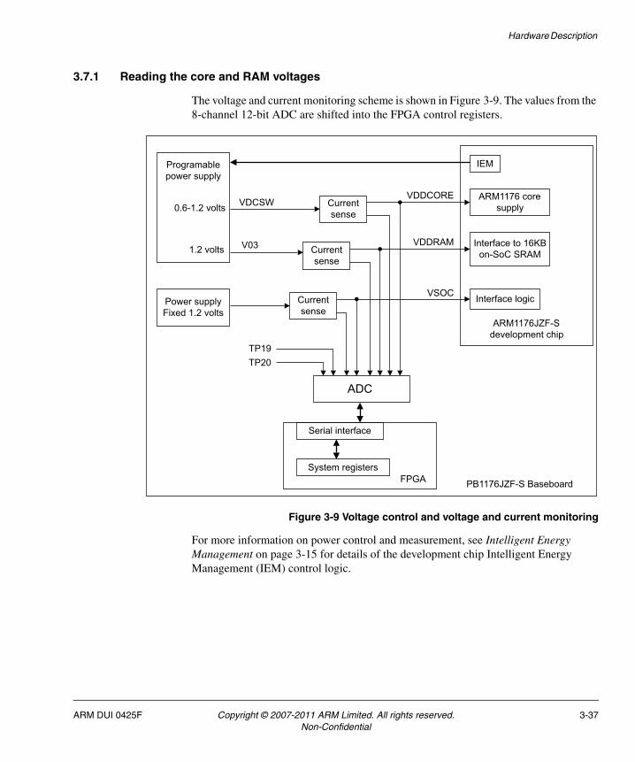
Hardware Description
3.7.1 Reading the core and RAM voltages
The voltage and current monitoring scheme is shown in Figure 3-9. The values from the 8-channel 12-bit ADC are shifted into the FPGA control registers.
Figure 3-9 Voltage control and voltage and current monitoring
For more information on power control and measurement, see Intelligent Energy Management on page 3-15 for details of the development chip Intelligent Energy Management (IEM) control logic.
VDDCORE
Programable power supply
VDDRAM
TP19
PB1176JZF-S Baseboard
ADC
FPGASystem registers
Current sense
Current sense
Serial interface
Current sense
VSOC
TP20
IEM
ARM1176JZF-S development chip
ARM1176 core supply
Interface to 16KB on-SoC SRAM
Interface logicPower supplyFixed 1.2 volts
0.6-1.2 volts
1.2 volts
VDCSW
V03
ARM DUI 0425F Copyright © 2007-2011 ARM Limited. All rights reserved. 3-37Non-Confidential

Hardware Description
3.8 Clock architecture
The clock domains for the PB1176JZF-S are shown in Figure 3-10.
Figure 3-10 Clock architecture for PB1176JZF-S
Ethernet
ARM1176JZF-S Dev. Chip
USB
PCI connector
Versatile Logic Tile expansion connectors SRAM Cellular
DRAM
25MHz xtal
Audio CODEC
24.576MHz xtal
24MHz reference
24MHz xtal
FPGA
PCI controller
Memory clocks
AXI bus clocks
AACIC
lock
sel
ectio
n an
d co
ntro
lUART,
KMI, SSP, SCI,
MMC, and serial bus
clocks
Programable oscillators
OSC0-OSC4
RTC
Clock selection and
dividers
PB1176JZF-S
USB config
6MHz xtal
JTAG
TimersDivide by 24
32kHz oscillator
Control signals
OSCCLK[4:0]
Configuration signals
PCI clock
AACI clock
AXI Mux and Demux
master
SCI
UARTs
SSP
ARM1176JZF-S core
1Hz clockRTC
PLLREFCLK2
CLCDOSCCLK[0]
OSCCLK2
ISP clock
masterISP
clock slave
AXI Mux and Demux
slaveOSCCLK3
24MHz
24MHz
24MHz
1MHz
PLLREFCLK
OSCCLK1 PLLREFCLK1
3-38 Copyright © 2007-2011 ARM Limited. All rights reserved. ARM DUI 0425FNon-Confidential

Hardware Description
The following sections describe:
• FPGA Peripheral clocks
• ARM1176JZF-S development chip clocks on page 3-40
• ICS307 programmable clock generators on page 3-48
For details on Logic Tile clocks, see Appendix C RealView Logic Tile.
3.8.1 FPGA Peripheral clocks
Table 3-5 lists the memory and peripheral clocks for the PB1176JZF-S FPGA.
Note OSCCLK[4] connects to the FPGA, but is not used by the system.
Table 3-5 FPGA clocks
Clock signal Frequency Description Source
OSCCLK[3:0] 6–75MHz References for development chip clocks and FPGA peripherals. (See also ARM1176JZF-S development chip clocks on page 3-40.)
The clock values are set by configuration registers in the FPGA. The register contents are automatically sent to the oscillators over a dedicated serial link (see ICS307 programmable clock generators on page 3-48).
Crystal oscillator
AACIBITCLK 12.288MHz This is the synchronization clock from the audio CODEC. The clock is an input to the AACI PrimeCell.
Crystal oscillator
ETHLCLK 24MHz ETHLCLK synchronizes data transfers between the external controller and the FPGA. (The Ethernet controller uses a 25MHz crystal for clocking signals to and from the Ethernet connector.)
24MHz reference
REFCLK32K 32.768kHz (fixed)
A 1Hz clock is generated from this signal. 32.768kHz crystal
PCICLK 33MHz This is the clock from the PCI backplane. PCI
ARM DUI 0425F Copyright © 2007-2011 ARM Limited. All rights reserved. 3-39Non-Confidential

Hardware Description
3.8.2 ARM1176JZF-S development chip clocks
This section describes the clocks used by the ARM1176JZF-S development chip (see Figure 3-11).
Figure 3-11 Development chip clocks
Table 3-6 on page 3-41 lists the major development chip clock signals.
DCG clock selection and divider logic
AXI subsystem
APB subsystem
ACLKEXT
ACLK_MSTOff-chip AXI masterto multiplexer
OSCCLK[3]OSCCLK[1]OSCCLK[2]
IEM and DVC
OSCCLK[0] CLCD controller
RTC
Timers
SCI
UARTS
SSP
1Hz clock1MHz clock
24MHZ clock
Values in SYS_CFGDATAx
registers
System controller
PL340 DMC
PL093 SMC
ARM1176JZF core
ACLK
ACLK_MST
ACLKX2 DDR_CLK[1:0]
CLK_POS_UP_OUTOff-chip AXI slave
CORECLK
APCCLCDCLK
APC_REFCLK_C
SCICLKIN
UARTCLK
PLLREFCLK
PLLREFCLK1
PLLREFCLK2
SSPCLKIN
TIMCLK
CLK1HZ
SMCLK[5:0]
PCLK
SMCCLK
24MHZ clock24MHZ clock
SMCMEMCLK
24MHZ clock
Configuration block signals
3-40 Copyright © 2007-2011 ARM Limited. All rights reserved. ARM DUI 0425FNon-Confidential

Hardware Description
Table 3-6 ARM1176JZF-S development chip clocks
Clock signal Frequency Description Source
PLLREFCLK 6–75MHz Reference for the master PLL. ICS307 OSC3
PLLREFCLK1 6–50MHz Reference clock for PLL1. ICS307 OSC1
PLLREFCLK2 6–40MHz Reference clock for PLL2. ICS307 OSC2
PLLFIXEDCLK 6–320MHz Reference clock for internal clock dividers.
PLLFIXEDCLK is an internal clock that has a frequency equal to PLLREFCLK times the divider values in ACLKEXTDIVSLV and ACLKDIV.
Internal (PLLREFCLK)
CORECLK 6–320MHz Core CPU clock. The operating frequency is PLLFIXEDCLK for 100% performance mode.
PLLREFCLK1 or PLLREFCLK2 are used by the IEM as the reference in power saving mode.
Internal (PLLREFCLK)
ACLK_MST 1–320MHz External AXI master clock that drives the AXIM multiplexor and is fed to the FPGA for timing the AXIS demultiplexor. (A programmable divider in the development chip determines the ratio between this clock and ACLK.)
ICS307 OSC3 (PLLREFCLK)
ACLK 3–160MHz Internal AXI master clock to the on-chip peripherals. (A programmable divider in the development chip determines the ratio between this clock and PLLFIXEDCLK.)
ICS307 OSC3 (PLLREFCLK)
ACLKEXT (CLK_POS_UP_OUT)
6–75MHz External AXI slave clock to Logic Tile. (Because of the PLL feedback circuit, this clock is at the same frequency as PLLREFCLK.)
ICS307 OSC3 (PLLREFCLK)
DDR_CLK[1:0] 3–320MHz The dynamic memory clocks from the DMC in the development chip. (ACLKX2 is the internal reference for the memory clocks)
DMC controller
SMCLK[5:0] 3–320MHz The static memory clocks from the SSMC in the development chip. (SMCMEMCLK is reference for the external static memory clocks)
SSMC controller
TIMCLK 1MHz The timers use the external 1MHZ clock as reference. (The FPGA contains a divider that generates this from 24MHz.)
24MHz reference clock
CLCDCLK 6–75MHz Reference for the CLCD controller. ICS307 OSC0
ARM DUI 0425F Copyright © 2007-2011 ARM Limited. All rights reserved. 3-41Non-Confidential

Hardware Description
CLK1HZ 1Hz The Real Time Clock uses this signal. 24MHz reference clock
UARTCLK 24MHz The UART reference clock. 24MHz reference clock
SCIREFCLKEXT 24MHz The clock for PL131 SCI in the development chip can be derived from this input.
24MHz reference clock
SCICLKIN 24MHz The SCI reference clock. 24MHz reference clock
SSPCLKIN 24MHz The SSP reference clock. 24MHz reference clock
APC_REFCLK_C 24MHz Power Management clock reference 24MHz reference clock
Table 3-6 ARM1176JZF-S development chip clocks (continued)
Clock signal Frequency Description Source
3-42 Copyright © 2007-2011 ARM Limited. All rights reserved. ARM DUI 0425FNon-Confidential
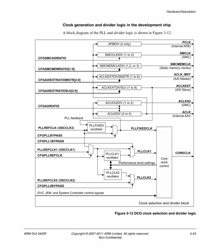
Hardware Description
Clock generation and divider logic in the development chip
A block diagram of the PLL and divider logic is shown in Figure 3-12.
Figure 3-12 DCG clock selection and divider logic
ACLKDIV (2 or 4)
PLLFIXED oscillatorPLLREFCLK (OSCCLK3)
CFGAXIEXTRATIOMSTR[2:0]
CFGAXIRATIO
CORECLK
ACLK
ACLKEXT
APBDIV (2 only) PCLK
ACLKEXTDIVSMSTR (1 to 8)ACLK_MST
CFGAXIEXTRATIOSLV[2:0]
SMCMEMCLKDIV (1,2, or 3) SMCMEMCLK
SMCCLKDIV (1 or 2) SMCLK
ACLKEXTDIVSLV (1 to 8)
CFGSMCAXIRATIO
CFGSMCMEMRATIO[1:0]
ACLKX2DIV (1 or 2) ACLKX2
PLLREFCLK1 (OSCCLK1)
PLLREFCLK2 (OSCCLK2)
CFGPLLBYPASS
CFGPLLREFCLK PLLCLK1oscillator
PLLCLK2oscillator
CFGPLL2BYPASS
CFGPLL1BYPASS
Performance level settingsCore clock
control
PLLFIXEDCLK
PLLCLK1
PLLCLK2
PLL feedback
DVC, IEM, and System Controller control signals
Clock selection and divider block
(AXI Slave)
(AXI Master)
(DMC)
(Internal AXI)
(Internal APB)
(SMC)
(Static memory clocks)
ARM DUI 0425F Copyright © 2007-2011 ARM Limited. All rights reserved. 3-43Non-Confidential

Hardware Description
The PLL block contains the three PLLs as shown in Figure 3-12 on page 3-43:
• PLLFIXED is configured at reset through the Configuration Block, and generates all fixed clocks in the design. PLLFIXED also clocks the IEM subsystem when running in 100% performance mode or when IEM is disabled. PLLREFCLK is the fixed reference to the PLLFIXED and ACLKEXT is the feedback clock.
• PLL1 and PLL2 generate clocks for sub-100% performance levels when IEM is enabled. The reference clock for PLL1 and PLL2 is determined by the configuration input CFGPLLREFCLK. If it is set LOW, the reference clock for PLL1 and PLL2 is PLLREFCLK. If HIGH, PLLREFCLK1 is the reference. The PLL frequency is based on a lookup table that contains divider values and voltage ranges for the different performance level settings.
The development chip contains programmable dividers that generate clock frequencies required by the various subsystems on the chip. The divisors are set by the external configuration signals that are controlled by the chip configuration registers (see Configuration registers SYS_CFGDATAx on page 4-45).
Note The frequency of ACLKEXT is always equal to PLLREFCLK if the PLL is not bypassed.
The feedback route to the PLL goes through both the ACLKEXTDIVSLV and ACLKDIV dividers as shown in Figure 3-12 on page 3-43, so increasing the divisor value for ACLKEXTDIVSLV or ACLKDIV increases the frequency of PLLFIXEDCLK rather than lowering the frequency of ACLKEXT.
The frequency of PLLFIXEDCLK is therefore:
PLLREFCLK * (ACLKEXTDIVSLV divisor) * (ACLKDIV divisor)
If a high clock rate is used for PLLREFCLK and high divisor values are loaded into ACLKEXTDIVSLV and ACLKDIV, the resulting high core clock speed might cause unreliable operation.
If CFGPLLBYPASS is HIGH, the PLLFIXED oscillator is bypassed and:
• PLLFIXEDCLK is equal to the PLLREFCLK input frequency
• the ACLK frequency is PLLREFCLK divided by the ACLKDIV divisor
• the ACLKEXT frequency is ACLK divided by the ACLKEXTDIVSLV divisor.
3-44 Copyright © 2007-2011 ARM Limited. All rights reserved. ARM DUI 0425FNon-Confidential

Hardware Description
The clock dividers for the AXI subsystem and memory controllers are:
ACLKDIV This block generates the ACLK that provides the clocks and enables for the internal AXI subsystem. The frequency of ACLK is:
• PLLFIXEDCLK / 2 if CFGAXIRATIO = 0
• PLLFIXEDCLK / 4 if CFGAXIRATIO = 1.
ACLKX2DIV
This block generates the double-rate ACLKX2 clock required for the PL340 dynamic memory controller. The frequency of ACLKX2 is:
• PLLFIXEDCLK if CFGAXIRATIO = 0
• PLLFIXEDCLK / 2 if CFGAXIRATIO = 1.
The PL340 divides this clock by two internally to regenerate a local AXI clock. Both ACLKX2DIV and ACLKDIV are controlled by the CFGAXIRATIO input so the DMC controller clock is always twice ACLK.
APBDIV The APB divide ratio is fixed. The APB PCLK frequency is always ACLK/2.
ACLKEXTDIVSLV
Generates the ACLKEXT clock for the off-chip AXI slave port. It also generates the PLL feedback clock that de-skews the system clock and enables the AXI slave ports to operate synchronously with off-chip devices.
ACLKEXT = ACLK / (ACLKEXTDIVSLV divisor)
but since ACLKEXT is always equal to PLLREFCLK,
ACLK = PLLREFCLK * (ACLKEXTDIVSLV divisor)
ACLKEXTDIVSMSTR
Generates the clock and enable for the off-chip AXI master port.
Table 3-7 ACLKEXTDIVSLV divisor values
CFGAXIEXTRATIOSLV[2:0] input b000 b001 b010 b011 b100 b101 b110 b111
ACLKEXTDIVSLV divisor 1 2 3 4 5 6 7 8
ARM DUI 0425F Copyright © 2007-2011 ARM Limited. All rights reserved. 3-45Non-Confidential

Hardware Description
ACLK_MST = ACLK / (ACLKEXTDIVMSTR divisor)
Caution The same divisor must be used for both ACLKEXTDIVMSTR and
ACLKEXTDIVSLV.
The external slave and master buses must operate at the same frequency. If different values are used for the divisors, the system will not function until the baseboard is power cycled and the default divisors are reloaded.
SMCCLKDIV
This block generates the AXI clock for the SMC PL093. The frequency of SMCCLK is:
• ACLK if CFGSMCAXIRATIO = 0
• ACLK / 2 if CFGSMCAXIRATIO = 1.
SMCMEMCLKDIV
This block generates the external memory clock for the SMC PL093:
SMCMEMCLK = ACLK / (SMCMEMCLKDIV divisor)
Default clock divider settings
The default configuration options are:
• PLLREFCLK is 35MHz
(This the default frequency for OSCCLK[3], see ICS307 programmable clock generators on page 3-48 and Oscillator registers, SYS_OSCx on page 4-42.)
• ACLKEXTDIVSLV divisor is 3
(See Configuration registers SYS_CFGDATAx on page 4-45f or more information on system configuration options and defaults.)
Table 3-8 ACLKEXTDIVMSTR divisor values
CFGAXIEXTRATIOMSTR[2:0] input b000 b001 b010 b011 b100 b101 b110 b111
ACLKEXTDIVMSTR divisor 1 2 3 4 5 6 7 8
Table 3-9 SMCMEMCLKDIV divisor values
CFGSMCMEMRATIO[1:0] input b00 b01 b10
SMCMEMCLKDIV divisor 1 2 3
3-46 Copyright © 2007-2011 ARM Limited. All rights reserved. ARM DUI 0425FNon-Confidential

Hardware Description
• ACLKDIV divisor is 2
(ACLKX2DIV is automatically set to 1 it shares the CFGAXIRATIO signal.)
• ACLKEXTDIVSMSTR divisor is 3
• SMCCLKDIV divisor is 1
• SMCMEMCLKDIV divisor is 3.
The default configuration results in the following frequencies:
• ACLKEXT=35MHz
(The slave clock frequency is always equal to the frequency of PLLREFCLK.)
• PLLFIXEDCLK=210MHz which is 3 * 2 * 35MHz
(For normal operation, the clock control selects PLLFIXEDCLK as CORECLK so this is the frequency of the ARM1176JZF-S core.)
• ACLK=105MHz which is PLLFIXEDCLK / 2
• ACLKX2=210MHz
(ACLKX2 is always two times ACLK, but the signal is divided by two inside the DMC to provide an internal AXI reference clock.)
• ACLK_MST=35MHz which is ACLK / 3
(This is the frequency of the external AXI master.)
• SMCCLK=105MHz which is ACLK / 1
• SMCMEMCLK=35MHz which is ACLK / 3
(This is buffered and provides SMCLK[5:0] to the external static memory.)
• PCLK=52.5MHz which is ACLK / 2 (this is a fixed-ratio divider).
Development chip Dynamic Clock Generator
The DCG generates all clocks, resets, power and clamp signals, and sequencing for the chip. You can use it for IEM or for performance measurements. The DCG consists of three PLLs as shown in Figure 3-12 on page 3-43. One PLL has a fixed frequency at reset, and the other two are variable. The fixed PLL clocks the processor at the 100% performance level, and the variable PLLs are used for all sub 100% performance levels. The fixed PLL is also used for the AXI, APB, and other fixed system clocks.
Two variable PLLs are required to enable the most efficient method of switching between two sub-100% performance levels. For example, if the performance level is currently set at 95%, the system runs on one of the variable PLLs. A request is then
ARM DUI 0425F Copyright © 2007-2011 ARM Limited. All rights reserved. 3-47Non-Confidential
Hardware Description
issued to drop to 90%. If there was only one variable PLL, it must be reconfigured to provide the 90% clock. The system must therefore switch to the fixed PLL while waiting for the variable PLL to lock at the new 90% performance frequency. However, the current voltage might not be sufficient to support the fixed PLL 100% performance frequency. Therefore using two variable PLLs allows the system to run at the current performance on one PLL, while the other PLL locks to the new performance level.
The DCG operates in open loop mode and uses fixed supply voltages based on a pre-defined voltage table programmed in the APC1 Open-loop VDD Core Registers.
Note The DCG IP block typically has both open loop and closed loop operating modes, but only the open loop mode is implemented in the development chip.
The DCG can operate with or without Performance Requirement Optimization. If Performance Requirement Optimization is enabled, the current voltage from the DVC, IECCRNTDVCIDX, and IEC configuration mapping IECCFGDVCIDXMAP, determine if the target frequency on IECTGTDCGIDX can be achieved at the current voltage. If the performance level is achievable, the PLL controller can immediately prepare the PLLs and switch when ready. If the required voltage is not available for the target frequency, the PLL controller switches to the highest available frequency for the current voltage. However, if the current frequency is at the maximum for the current voltage, the PLL controller prepares to switch to the maximum frequency for the next voltage step. This enables maximum performance to be achieved as the voltage level rises.
When switching to a lower performance level, the DCG can switch to the lower performance clock as soon as the PLL is ready. If a new performance target is issued by the IEC before the current target has successfully completed, the new target always overrides the current target.
3.8.3 ICS307 programmable clock generators
Five programmable (6–200 MHz) clocks are supplied to the FPGA by the programmable MicroClock ICS307 clock generators (OSC0–OSC4):
OSCCLK0 This is the reference clock for the CLCDC.
OSC0 uses a 24MHz crystal as its reference. A fixed-frequency 24MHz signal, REFCLK24MHZ, is output from OSC0 and used as a reference signal for:
• The input for programmable oscillators OSC1–OSC4.
• the Ethernet controller clock (the Ethernet serial data clock is generated from a 25MHz crystal on the Ethernet controller).
3-48 Copyright © 2007-2011 ARM Limited. All rights reserved. ARM DUI 0425FNon-Confidential

Hardware Description
• the USB controller clock
• the USB debug controller clock
• the external peripheral clocks for the SCI, UART, and SSP in the ARM1176JZF-S development chip.
• the input to divide-by-24 logic in the FPGA that produces the 1MHz reference clock for the timers.
OSCCLK1 This is the reference for the ARM1176JZF-S development chip PLLREFCLK1. (This clock can be selected by the IEM system to reduce power consumption.)
OSCCLK2 This is the reference for the ARM1176JZF-S development chip PLLREFCLK2. (This clock can be selected by the IEM system to reduce power consumption.)
OSCCLK3 This is the reference for the ARM1176JZF-S development chip PLLREFCLK. This is the master reference clock used to generate the AXI clocks, APB clock, and the memory controller clocks. (If operating in 100% power mode with IEM off, this is also the reference for the core clock PLL.)
OSCCLK4 This is the reference to the FPGA. (It is not used in the reference implementation.)
The output frequencies of the ICS307s are controlled by divider values loaded into the serial data input pins on the oscillators. The divider values are defined by the SYS_OSCx and SYS_OSCRESETx registers. The data stream and register format is shown in Figure 3-13. See Oscillator registers, SYS_OSCx on page 4-42 for details on the clock control registers.
Figure 3-13 Serial data and SYS_OSCx register format
Note Bit 23 is loaded into the shift register first and bit 0 is loaded last. Data is clocked into the ICS307DATA pins of the oscillators on the rising edge of ICS307CLK. One of the ICS307STRB[4:0] signals is pulsed HIGH to latch the serial data into the divider control register.
ARM DUI 0425F Copyright © 2007-2011 ARM Limited. All rights reserved. 3-49Non-Confidential

Hardware Description
You can calculate the oscillator output frequency from the formula:
where:
VDW Is the VCO divider word (4 – 511) from SYS_OSCx[8:0]
RDW Is the reference divider word (1 – 127) from SYS_OSCx[15:9]
DIVIDE Is the divide ratio (2 to 10) selected from SYS_OSCx[18:16]:
• b000 selects divide by 10
• b001 selects divide by 2
• b010 selects divide by 8
• b011 selects divide by 4
• b100 selects divide by 5
• b101 selects divide by 7
• b110 selects divide by 3
• b111 selects divide by 6.
For more information on the ICS clock generator and a frequency calculator, see the ICS web site at www.icst.com. For details of the clock control registers, see FPGA status and system control registers on page 4-37.
CLKx = 48 * (VDW + 8)
(RDW + 2) * DIVIDEMHz
3-50 Copyright © 2007-2011 ARM Limited. All rights reserved. ARM DUI 0425FNon-Confidential

Hardware Description
3.9 Test, configuration, and debug interfaces
The following test and configuration interfaces are located on the PB1176JZF-S:
• JTAG, see JTAG debug port and USB config port support
• Logic analyzer, see Integrated logic analyzer on page 3-57
• Trace, see Embedded trace support on page 3-58
• Configuration switches and status indicators, see Configuration control on page 3-13 and User switches and LEDs on page 3-26
• Boot Monitor, see Appendix F Boot Monitor and platform library.
Note There are also test points and debug connectors for individual interface circuits. See Test and debug connections on page A-16.
3.9.1 JTAG debug port and USB config port support
The PB1176JZF-S supports debugging using embedded or external hardware. The debugging interface can be controlled by:
JTAG hardware
The RealView Debugger for example, use an external interface box, such as RealView ICE to connect to the JTAG connector. If you are using an external JTAG debug tool, the USB config port is disabled.
USB config port
The USB config port is embedded on the PB1176JZF-S and can be used for loading FPGA or PLD images. It cannot, however, be used to debug applications running in the processor core. The PC and the PB1176JZF-S are connected by a standard USB cable.
Note With reference to the ground pin 20 of the JTAG connector. On the PB1176JZF-S, pin 20 connects to a pull-up resistor and the nICEDETECT signal. The USB config port is automatically disabled if a JTAG emulator is connected and nICEDETECT is LOW. If you are using third-party debugging hardware, ensure that a ground is present on pin 20 of the JTAG connector.
ARM DUI 0425F Copyright © 2007-2011 ARM Limited. All rights reserved. 3-51Non-Confidential
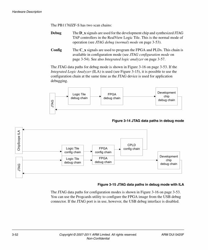
Hardware Description
The PB1176JZF-S has two scan chains:
Debug The D_x signals are used for the development chip and synthesized JTAG TAP controllers in the RealView Logic Tile. This is the normal mode of operation (see JTAG debug (normal) mode on page 3-53).
Config The C_x signals are used to program the FPGA and PLDs. This chain is available in configuration mode (see JTAG configuration mode on page 3-54). See also Integrated logic analyzer on page 3-57.
The JTAG data paths for debug mode is shown in Figure 3-16 on page 3-53. If the Integrated Logic Analyzer (ILA) is used (see Figure 3-15), it is possible to use the configuration chain at the same time as the JTAG device is used for application debugging.
Figure 3-14 JTAG data paths in debug mode
Figure 3-15 JTAG data paths in debug mode with ILA
The JTAG data paths for configuration modes is shown in Figure 3-16 on page 3-53. You can use the Progcards utility to configure the FPGA image from the USB debug connector. If the JTAG port is in use, however, the USB debug interface is disabled.
JTA
G
Logic Tiledebug chain
FPGAdebug chain
Development chip
debug chain
JTA
G
Logic Tiledebug chain
FPGAconfig chain
Chi
pSco
pe IL
A
Development chip
debug chain
CPLDconfig chainLogic Tile
config chain
FPGAdebug chain
3-52 Copyright © 2007-2011 ARM Limited. All rights reserved. ARM DUI 0425FNon-Confidential

Hardware Description
Note You can use the ILA to debug a user design in the Logic Tile, using chipscope or other FPGA debug tools.
Figure 3-16 JTAG data paths in config mode
JTAG debug (normal) mode
During normal operation and software development, the PB1176JZF-S operates in debug mode. (The CONFIG switch is in the default OFF position, see Connecting JTAG, Trace, and configuration equipment on page 2-10.) In debug mode:
• The signal nCFGEN to the Logic Tile connector is HIGH
• The CONFIG LED is off on the PB1176JZF-S (and on each tile in the stack)
• The JTAG signals are routed through the ARM1176JZF-S development chip
• The JTAG scan path is rerouted sequentially to:
— Logic Tile debug scan chain (D_x signals) if a tile is connected
— FPGA debug scan chain (D_x signals)
— ARM1176JZF-S debug unit scan chain.
• A debugger, RealView Debugger for example, controls the scan chain
• The FPGAs are not visible on the scan chain unless they contain debuggable devices. If an ILA is used, the FPGA can be configured at the same time as the JTAG debugger is used with the ARM cores.
• If RealView Logic Tiles are present and have debuggable devices, the D_x signals are part of their JTAG scan chain.
• The FPGAs in the system load their images from configuration flash.
JTA
G
Logic Tileconfig chain
FPGAconfig chainUSB
debug switches
US
B
debu
g USB debug controller
Development chip
config chain
CPLDconfig chain
ARM DUI 0425F Copyright © 2007-2011 ARM Limited. All rights reserved. 3-53Non-Confidential

Hardware Description
JTAG configuration mode
This mode is selected if the CONFIG switch is ON. (See Connecting JTAG, Trace, and configuration equipment on page 2-10.) In configuration mode:
• The signal nCFGEN to the Logic Tile connector is LOW.
• The CONFIG LED is lit on the PB1176JZF-S (and on each tile in the stack).
• The JTAG scan path is rerouted sequentially to:
— Logic Tile configuration scan chain (C_x signals) if a tile is connected
— FPGA configuration scan chain (C_x signals)
— Configuration CPLD scan chain
— ARM1176JZF-S test chip boundary scan chain.
• A configuration utility, ProgCards for example, controls the scan chain.
• If RealView Logic Tiles are present, the C_x signals are part of the JTAG scan chain.
• All FPGAs and PLDs in the system (including any devices in a RealView Logic Tile if present) are added into the scan chain.
• The TAP controller in the ARM1176JZF-S development chip is not visible and is replaced by a Boundary Scan TAP controller that is used for board-level production testing.
• This enables the board to be configured or upgraded in the field using JTAG equipment or the onboard USB config port.
• The nonvolatile PLDs devices can be reprogrammed directly by JTAG.
• FPGA images can be loaded from the scan chain.
The FPGAs are volatile. In normal mode, they load their configuration from nonvolatile flash memory. In configuration mode, they can be loaded from either JTAG or the configuration flash memory.
Note The configuration flash memory does not have a JTAG port, but it can be
programmed using JTAG by loading a flash-loader design into the FPGAs and PLDs. The flash-loader can then transfer data from the JTAG programming utility to the configuration flash.
3-54 Copyright © 2007-2011 ARM Limited. All rights reserved. ARM DUI 0425FNon-Confidential

Hardware Description
Caution Third party JTAG debug equipment may not support this method of programming
configuration flash, where possible, you must use ARM RealView ICE or the USB config port.
After configuration you must:
1. switch OFF the CONFIG switch
2. power cycle the development system.
JTAG signals
Table 3-10 provides a description of the JTAG and related signals.
Note In the description in Table 3-10, the term JTAG equipment refers to any hardware that can drive the JTAG signals to devices in the scan chain. Typically this is RealView ICE, or the embedded USB debug logic.
Table 3-10 JTAG related signals
Name Description Function
TDI Test data in
(from JTAG equipment)
TDI and TDO connect each component in the scan chain.
TDO Test data out
(to JTAG equipment)
TDO is the return path of the data input signal TDI. The JTAG components are connected in the return path so that the length of track driven by the last component in the chain is kept as short as possible.
TMS Test mode select
(from JTAG equipment)
TMS controls transitions in the TAP controller state machine.
TCK Test clock
(from JTAG equipment)
TCK synchronizes all JTAG transactions. TCK connects to all JTAG components in the scan chain. Series termination resistors are used to reduce reflections and maintain good signal integrity.
ARM DUI 0425F Copyright © 2007-2011 ARM Limited. All rights reserved. 3-55Non-Confidential
Hardware Description
RTCK Return TCK
(to JTAG equipment)
Some devices sample TCK and delay the time at which a component actually captures data. Using a mechanism called adaptive clocking, the RTCK signal is returned by the core to the JTAG equipment, and the TCK is not advanced until the core has captured the data. In adaptive clocking mode, RealView ICE waits for an edge on RTCK before changing TCK. In a multiple device JTAG chain, the RTCK output from a component connects to the TCK input of the next device in the chain.
nCFGEN Configuration enable
nCFGEN is an active LOW signal used to put the boards into configuration mode. In configuration mode all FPGAs and PLDs are connected to the scan chain so that they can be configured by the JTAG equipment. (The TAP controller in the PB1176JZF-S is not accessible.)
nSRST System reset
(bidirectional)
nSRST is an active LOW open-collector signal that can be driven by the JTAG equipment to reset the target board. Some JTAG equipment senses this line to determine when a board has been reset by the engineer.
This is also used in configuration mode to control the initialization pin (nINIT) on the FPGAs.
Though not a JTAG signal, nSRST is described because it can be controlled by JTAG equipment.
nTRST Test reset
(from JTAG equipment)
This active LOW open-collector signal resets the JTAG port and the associated debug circuitry on the ARM1176JZF-S development chip. It is asserted at power-up, and can be driven by the JTAG equipment. This signal is also used in configuration mode to control the programming pin, nPROG, on FPGAs.
DBGRQ Debug request
(from JTAG equipment)
DBGRQ is a request for the processor core to enter the debug state. It is provided for compatibility with third-party JTAG equipment.
Table 3-10 JTAG related signals (continued)
Name Description Function
3-56 Copyright © 2007-2011 ARM Limited. All rights reserved. ARM DUI 0425FNon-Confidential

Hardware Description
The JTAG path chosen depends on whether the system is in configuration mode or debug mode. The CONFIG link controls the nCFGEN signal that is routed through the PB1176JZF-S and tile connectors.
3.9.2 Integrated logic analyzer
The ILA connector (J11) enables you to connect a ChipScope compatible analyzer to the configuration scan chain while a JTAG debugger connects to the debug scan chain. This enables you to debug the FPGAs on stacked tiles while examining code on the CPU.
Note In debug mode:
• the ILA connector is enabled
• the FPGA on the baseboard is excluded from the configuration scan chain.
In configuration mode:
• the ILA connector is disabled
• the FPGA on the baseboard is included in the configuration scan chain.
For more details on the integrated logic analyzer, see the ChipScope details on the Xilinx website (www.xilinx.com).
DBGACK Debug acknowledge
(to JTAG equipment)
DBGACK indicates to the debugger that the processor core has entered debug mode. It is provided for compatibility with third-party JTAG equipment.
GLOBAL_DONE FPGA configured GLOBAL_DONE is an open-collector signal that indicates when FPGA configuration is complete. Although this signal is not a JTAG signal, it does affect nSRST. The GLOBAL_DONE signal is routed between all RealView boards.
nRTCKEN Return TCK enable
nRTCKEN is an active LOW signal driven by any tile that requires RTCK to be routed back to the JTAG equipment. If nRTCKEN is HIGH, the baseboard drives RTCK LOW. If nRTCKEN is LOW, the baseboard drives the TCK signal back to the JTAG equipment.
Table 3-10 JTAG related signals (continued)
Name Description Function
ARM DUI 0425F Copyright © 2007-2011 ARM Limited. All rights reserved. 3-57Non-Confidential

Hardware Description
3.9.3 Embedded trace support
The ARM1176JZF-S development chip incorporates an ARM11 Embedded Trace Macrocell (ETM11). This enables you to carry out real-time debugging by connecting external trace equipment to the Trace connectors on the PB1176JZF-S. To trace program flow, the ETM broadcasts branch addresses, data accesses, and status information through the trace port. Later in the debug process, the complete instruction flow can be reconstructed by the RealView Debugger.
Note Connection of the trace port analyzer is described in Connecting the Trace Port Analyzer on page 2-13.
A trace connector is also provided for the Logic Tile. Use the Logic Tile trace connector to either:
• monitor trace activity in a processor implemented in the Logic Tile FPGA
• monitor signal activity on the header connector.
3-58 Copyright © 2007-2011 ARM Limited. All rights reserved. ARM DUI 0425FNon-Confidential

Chapter 4 Programmer’s Reference
This chapter describes the memory map and the configuration registers for the peripherals in the ARM1176JZF-S development chip. It contains the following sections:
• Memory map on page 4-3
• ARM1176JZF-S development chip system controller on page 4-12
• Advanced Power Controller and Power Management Interface on page 4-22
• Advanced Audio CODEC Interface, AACI on page 4-27
• Character LCD display on page 4-29
• Color LCD Controller, CLCDC on page 4-32
• Dynamic Memory Controller, DMC on page 4-34
• Ethernet on page 4-36
• FPGA status and system control registers on page 4-37
• General Purpose Input/Output, GPIO on page 4-57
• Interrupt controllers in the ARM1176JZF-S development chip on page 4-58
• Interrupt controllers in the FPGA on page 4-74
• Level 2 Cache Controller on page 4-106
• Keyboard and Mouse Interface, KMI on page 4-107
• MultiMedia Card Interfaces, MCI on page 4-108
ARM DUI 0425F Copyright © 2007-2011 ARM Limited. All rights reserved. 4-1Non-Confidential

Programmer’s Reference
• PCI controller on page 4-109
• Real Time Clock, RTC on page 4-120
• Serial bus interface on page 4-121
• Smart Card Interface, SCI on page 4-123
• Synchronous Serial Port, SSP on page 4-124
• Synchronous Static Memory Controller, SSMC on page 4-126
• System Controller on page 4-130
• Timers on page 4-131
• TrustZone Protection Controller on page 4-132
• USB interface on page 4-142
• UART on page 4-140
• Watchdog on page 4-143.
For detailed information on the programming interface for ARM PrimeCell peripherals and controllers, see the appropriate technical reference manual. For the interrupt signals and release versions of ARM IP, see the section of this chapter that describes the peripheral.
4-2 Copyright © 2007-2011 ARM Limited. All rights reserved. ARM DUI 0425FNon-Confidential

Programmer’s Reference
4.1 Memory map
The locations for memory, peripherals, and controllers are listed in Table 4-1 on page 4-4 and Figure 4-1 on page 4-11.
There are multiple buses in the ARM1176JZF-S development chip. Not all of the buses can access all of the memory regions.
Note The VFP coprocessors is not memory-mapped peripherals so it does not appear in the memory map listed in Table 4-1 on page 4-4. See the appropriate technical reference manual for more details.
See FPGA status and system control registers on page 4-37 and Boot Select Register, SYS_BOOTCS on page 4-51 for details on configuration operations that can be performed after the system has started. See also Configuration control on page 3-13 and Configuration registers SYS_CFGDATAx on page 4-45 for a description of how the development chip is configured at reset.
On reset, the ARM1176JZF-S development chip begins executing code at address 0x0. This address is normally volatile SDRAM. Remapping enables non-volatile static memory to be decoded for accesses to low memory.
Configuration switch S1 modifies the memory map of static memory at reset. See Boot memory selection on page 2-4.
Note There are two GIC interrupt controllers in the FPGA and a GIC and TrustZone interrupt controller in the development chip. Unless otherwise specified, the interrupt numbers in Table 4-1 on page 4-4 refer to inputs to the GICS in the FPGA. For more information on the interrupt signals, see Interrupt controllers in the ARM1176JZF-S development chip on page 4-58.
ARM DUI 0425F Copyright © 2007-2011 ARM Limited. All rights reserved. 4-3Non-Confidential

Programmer’s Reference
Table 4-1 Memory map
Peripheral Location Interrupta Address Size
Dynamic memory controller chip select 0
Note This is an alias of the memory at 0x08000000-0x0BFFFFFF.
Dev. chip - 0x00000000–
0x03FFFFFF
64MB
Dynamic memory controller chip select 1
Note This is an alias of the memory at 0x0C000000-0x0FFFFFFF.
Dev. chip - 0x04000000–
0x07FFFFFF
64MB
Dynamic memory controller chip select 2 Dev. chip - 0x08000000-0x0BFFFFFF
64MB
Dynamic memory controller chip select 3 Dev. chip - 0x0C000000-0x0FFFFFFF
64MB
System registers FPGA APB
- 0x10000000–
0x10000FFF
4KB
System controller FPGA APB
- 0x10001000–
0x10001FFF
4KB
Reserved (I2C serial bus control) - - 0x10002000– 0x10002FFF
4KB
FPGA TrustZone Protection Controller FPGA APB
- 0x10003000–
0x10003FFF
4KB
Advanced Audio CODEC Interface FPGA - 0x10004000–
0x10004FFF
4KB
MCI FPGA 33 0x10005000–
0x10005FFF
4KB
Keyboard/Mouse Interface 0 FPGA 35 0x10006000–
0x10006FFF
4KB
Keyboard/Mouse Interface 1 FPGA 36 0x10007000–
0x10007FFF
4KB
Character LCD Interface FPGA 39 0x10008000–
0x10008FFF
4KB
4-4 Copyright © 2007-2011 ARM Limited. All rights reserved. ARM DUI 0425FNon-Confidential
Programmer’s Reference
UART 4 FPGA 38 0x10009000–
0x10009FFF
4KB
Reserved for future use - - 0x1000A000–
0x1000DFFF
16KB
Smart Card Interface FPGA 37 0x1000E000–
0x1000EFFF
4KB
Serial Bus Interface FPGA - 0x1000F000–
0x1000FFFF
4KB
Reserved - - 0x10010000–
0x10010FFF
4KB
Reserved (FPGA timers 0 and 1) - - 0x10011000–
0x10011FFF
4KB
Reserved (FPGA timers 2 and 3) - - 0x10012000–
0x10012FFF
4KB
Reserved - - 0x10013000–
0x10013FFF
4KB
FPGA GPIO 1 FPGA 40 0x10014000–
0x10014FFF
4KB
Reserved (FPGA GPIO 2) FPGA 41 0x10015000–
0x10015FFF
4KB
Reserved - - 0x10016000–
0x10016FFF
4KB
Real Time Clock FPGA 57 0x10017000–
0x10017FFF
4KB
Reserved - - 0x10018000–
0x10018FFF
4KB
PCI controller configuration registers FPGA - 0x10019000–
0x10019FFF
4KB
Reserved - - 0x1001A000–
0x1001BFFF
8KB
Power Manager FPGA - 0x1001C000–
0x1001FFFF
16MB
Table 4-1 Memory map (continued)
Peripheral Location Interrupta Address Size
ARM DUI 0425F Copyright © 2007-2011 ARM Limited. All rights reserved. 4-5Non-Confidential
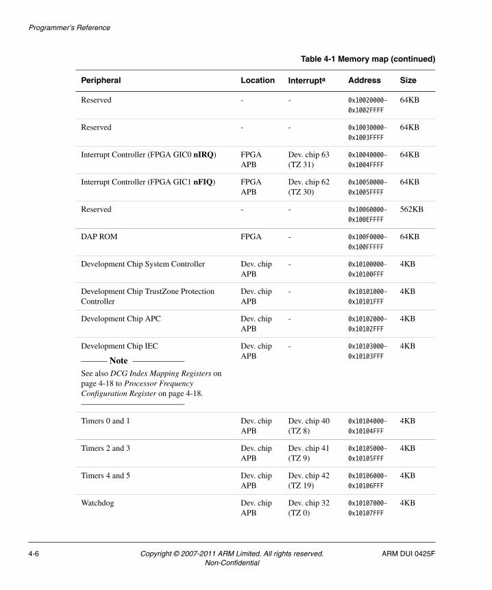
Programmer’s Reference
Reserved - - 0x10020000–
0x1002FFFF
64KB
Reserved - - 0x10030000–
0x1003FFFF
64KB
Interrupt Controller (FPGA GIC0 nIRQ) FPGA APB
Dev. chip 63 (TZ 31)
0x10040000–
0x1004FFFF
64KB
Interrupt Controller (FPGA GIC1 nFIQ) FPGA APB
Dev. chip 62 (TZ 30)
0x10050000–
0x1005FFFF
64KB
Reserved - - 0x10060000–
0x100EFFFF
562KB
DAP ROM FPGA - 0x100F0000–
0x100FFFFF
64KB
Development Chip System Controller Dev. chip APB
- 0x10100000–
0x10100FFF
4KB
Development Chip TrustZone Protection Controller
Dev. chip APB
- 0x10101000–
0x10101FFF
4KB
Development Chip APC Dev. chip APB
- 0x10102000–
0x10102FFF
4KB
Development Chip IEC
Note See also DCG Index Mapping Registers on page 4-18 to Processor Frequency Configuration Register on page 4-18.
Dev. chip APB
- 0x10103000–
0x10103FFF
4KB
Timers 0 and 1 Dev. chip APB
Dev. chip 40 (TZ 8)
0x10104000–
0x10104FFF
4KB
Timers 2 and 3 Dev. chip APB
Dev. chip 41 (TZ 9)
0x10105000–
0x10105FFF
4KB
Timers 4 and 5 Dev. chip APB
Dev. chip 42 (TZ 19)
0x10106000–
0x10106FFF
4KB
Watchdog Dev. chip APB
Dev. chip 32 (TZ 0)
0x10107000–
0x10107FFF
4KB
Table 4-1 Memory map (continued)
Peripheral Location Interrupta Address Size
4-6 Copyright © 2007-2011 ARM Limited. All rights reserved. ARM DUI 0425FNon-Confidential

Programmer’s Reference
Real Time Clock Dev. chip APB
Dev. chip 46 (TZ 14)
0x10108000–
0x10108FFF
4KB
DMC configuration registers Dev. chip APB
- 0x10109000–
0x10109FFF
4KB
Development chip GPIO 0 Dev. chip APB
Dev. chip 48 (TZ 16)
0x1010A000–
0x1010AFFF
4KB
SSP Interface Dev. chip APB
Dev. chip 49 (TZ 17)
0x1010B000–
0x1010BFFF
4KB
UART 0 Interface Dev. chip APB
Dev. chip 50 (TZ 18)
0x1010C000–
0x1010CFFF
4KB
UART 1 Interface Dev. chip APB
Dev. chip 51 (TZ 19)
0x1010D000–
0x1010DFFF
4KB
UART 2 Interface Dev. chip APB
Dev. chip 52 (TZ 20)
0x1010E000–
0x1010EFFF
4KB
UART 3 Interface Dev. chip APB
Dev. chip 53 (TZ 21)
0x1010F000–
0x1010FFFF
4KB
Level 2 Cache Controller configuration registers
Dev. chip Dev. chip 45 (TZ 13)
0x10110000–
0x10110FFF
4KB
Static Memory Controller configuration registers
Dev. chip - 0x10111000–
0x10111FFF
4KB
CLCD configuration registers Dev. chip Dev. chip 47 (TZ 15)
0x10112000–
0x10112FFF
4KB
Reserved - - 0x10113000–
0x1011EFFF
48KB
TZIC Dev. chip Dev. chip nFIQ
0x1011F000–
0x1011FFFF
4KB
GIC CPU interface Dev. chip Dev. chip nIRQ
0x10120000–
0x10120FFF
4KB
GIC distributor Dev. chip - 0x10121000–
0x10121FFF
4KB
Reserved Dev. chip - 0x10122000–
0x1012FFFF
56KB
Table 4-1 Memory map (continued)
Peripheral Location Interrupta Address Size
ARM DUI 0425F Copyright © 2007-2011 ARM Limited. All rights reserved. 4-7Non-Confidential

Programmer’s Reference
CoreSight ROM Table Dev. chip - 0x10130000–
0x10130FFF
4KB
CoreSight ETB Dev. chip - 0x10131000–
0x10131FFF
4KB
CoreSight ETM11 Dev. chip - 0x10132000–
0x10132FFF
4KB
CoreSight CTI0 Dev. chip - 0x10133000–
0x10133FFF
4KB
CoreSight CTI1 Dev. chip - 0x10134000–
0x10134FFF
4KB
CoreSight TPIU Dev. chip - 0x10135000–
0x10135FFF
4KB
Reserved Dev. chip - 0x10136000–
0x101FFFFF
79KB
RAM/ROM
Note 16KB on-SoC SRAM (NVRAM/Pseudo boot-ROM)
Dev. chip - 0x10200000–
0x10203FFF
16KB
Reserved - - 0x10204000–
0x102FFFFF
1MB
RAM (development chip)
512KB on-SoC SRAM (L3 RAM configurable secure region)
Dev. chip - 0x10300000–
0x1037FFFF
512KB
Reserved - - 0x10380000–
0x1FFFFFFF
252MB
SSMC Chip Select 0/7 PISMO Memory expansion
48 0x20000000–
0x23FFFFFF
64MB
SSMC Chip Select 1 PISMO Memory expansion
48 0x24000000–
0x27FFFFFF
64MB
Table 4-1 Memory map (continued)
Peripheral Location Interrupta Address Size
4-8 Copyright © 2007-2011 ARM Limited. All rights reserved. ARM DUI 0425FNon-Confidential

Programmer’s Reference
SSMC Chip Select 2 PISMO Memory expansion
48 0x28000000–
0x2BFFFFFF
64MB
SSMC Chip Select 3 PISMO Memory expansion
48 0x2C000000–
0x2FFFFFFF
64MB
SSMC Chip Select 4 NOR flash 2 Board - 0x30000000–
0x33FFFFFF
64MB
SSMC Chip Select 5 Cellular RAM (8MB fitted)
Board - 0x34000000–
0x37FFFFFF
64MB
SSMC Chip Select 6 FPGA Configuration flash
Board - 0x38000000–
0x39FFFFFF
32MB
SSMC Chip Select 6 Ethernet Board 32 0x3A000000–
0x3AFFFFFF
16MB
SSMC Chip Select 6 USB Board 33 0x3B000000–
0x3BFFFFFF
16MB
SSMC Chip Select 7 Secure NOR flash 1 Board - 0x3C000000–
0x3FFFFFFF
64MB
Internal RAM and ROM
Note 8KB FPGA AXI BOOTROM is available before the system has booted (hard-coded program in FPGA to setup system when no boot monitor present).
256KB FPGA SRAM is available after the system has booted.
FPGA - 0x40000000– 0x40001FFF
or
0x40000000– 0x4003FFFF
8KB
or
256KB
Reserved (Static memory)
Note The development chip has internal static memory at 0x10300000–0x1037FFFF and 0x40000000–0x4003FFFF.
The SSMC addresses external static memory at 0x20000000–0x37FFFFFF.
- - 0x40040000– 0x5FFFFFFF
512MB
Table 4-1 Memory map (continued)
Peripheral Location Interrupta Address Size
ARM DUI 0425F Copyright © 2007-2011 ARM Limited. All rights reserved. 4-9Non-Confidential

Programmer’s Reference
PCI interface Expansion PCI bus
44 PCI0
45 PCI1
46 PCI2
47 PCI3
0x60000000–
0x6FFFFFFF
256MB
Reserved - - 0x70000000–
0x7FFFFFFF
256MB
RealView Logic Tile expansion (AXI master bus)
Note If a RealView Logic Tile is installed, accesses in this range must be decoded by the tile. This is the recommended address range for placing memory-mapped peripherals in a RealView Logic Tile.
Board (RealView Logic Tile headers)
- 0x80000000–
0xFFFFFFFF
2GB
a. Interrupt numbers refer to the FPGA GICs unless otherwise specified. For interrupts to the development chip, the corresponding interrupt to the TZIC is given in parentheses. Interrupt numbers 0–31 are reserved for processor use on all GICs.
Table 4-1 Memory map (continued)
Peripheral Location Interrupta Address Size
4-10 Copyright © 2007-2011 ARM Limited. All rights reserved. ARM DUI 0425FNon-Confidential

Programmer’s Reference
Figure 4-1 shows the mem ory map. Configuration switch S7 modifies the memory map of static memory at reset. The memory map shown is with switches S7-1 and S7-2 set to OFF. (See Boot memory selection on page 2-4.)
Figure 4-1 Memory map
Power manager
DAP ROM
USB(CS6 0x3B000000)
Development ChipStatic memory(SSMC CSx)
FPGARegisters
FPGAPCI bus
Reserved
0x80000000
0xFFFFFFFF
0x60000000
0x10100000
0x40000000
Logic Tile expansion (AXI M)
8MB Cellular RAM (CS5 0x34000000)
64MB NOR flash (CS7 0x3C000000)
64MB Secure NOR flash
(CS4 0x30000000)
Static expansion(CS3 0x2C000000)
Static expansion (CS2 0x28000000)Static expansion
(CS1 0x24000000)Static expansion
(CS0 0x20000000)
0x10000000
0x00000000
Mobile DDR (DMC CS0)
0x10110000
0x70000000
Ethernet(CS6 0x3A000000)
SCI 0
UART 4Character LCD
KMI 1
AACI
KMI 0MCI 0
GIC0
PCI control
System registers
GPIO 1
RTC
Reserved
Memory is remapped at reset
to cover low memory address
Reserved
Reserved0x44000000
Reserved
System controller
TZ protection controller
Reserved
Serial Bus
Reserved
Reserved
Reserved
GIC1Reserved
Dev chip APB
0x20000000
APCIEC
System controller
TZ protection controller Dev Chip
peripherals
Timer01
WatchdogRTC
Timer23Timer45
DMC configGPIOSSP
UART0UART1UART2UART3
CoreSight ROM table
Reserved
CoreSight ETM11CoreSight CTI0
L2CCSMC config
Dev chip peripherals
CLCD config
TZICReserved
GIC CPU interfaceGIC distributor
Reserved
CoreSight ETB
CoreSight CTI1CoreSight TPIU
Dev chip reserved
Reserved
32MB config flash(CS6 0x38000000)
Remapped Static
Development Chip
FPGA
ARM DUI 0425F Copyright © 2007-2011 ARM Limited. All rights reserved. 4-11Non-Confidential

Programmer’s Reference
4.2 ARM1176JZF-S development chip system controller
This section describes the system controller registers located in the development chip. The registers are reset by power-on or by pressing the reset pushbutton.
Table 4-2 Development chip system controller registers
Register Address Access Reset Description
CoreID 0x10100000 Read only Variable Core identification register (the lower four bits are set by the values on the configuration pins)
SoCConfig1 0x10100004 Read/Write Variable SoC configuration register (set by values present on the configuration input pins when the chip is reconfigured)
SoCConfig2 0x10100008 Read only Variable SoC configuration register (set by values present on the configuration input pins when the chip is reconfigured)
SysControl 0x1010000C Read/Write Variable System controller control register
SysStatus 0x10100010 Read only Variable System status register
DCGIDXMAP0 0x10100014 Read/Write 0x00924924 IEC configuration index mapping configuration level 1-8
DCGIDXMAP1 0x10100018 Read/Write 0x00924924 IEC configuration index mapping configuration level 9-16
DCGIDXMAP2 0x1010001C Read/Write 0x00DADB6D IEC configuration index mapping configuration level 17-24
DCGIDXMAP3 0x10100020 Read/Write 0x00FFFFB6 IEC configuration index mapping configuration level 25-32
DCGPERFMAP0 0x10100024 Read/Write 0x00000000 Performance level mapping index 1-4
DCGPERFMAP1 0x10100028 Read/Write 0x806A5640 Performance level mapping index 5-8
DVCIDXMAP 0x1010002C Read/Write 0xFAC688 IEC configuration DVC index map levels 1-8
CFGFREQCPU 0x10100030 Read/Write 0x0004E200 Maximum CPU clock speed, 320MHz
CFGFREQDPM 0x10100034 Read/Write 0x00001D4C DPM frequency
PLLCFGPERF1 0x10100038 Read/Write 0x00000000 PLL configuration setting for performance level 1
PLLCFGPERF2 0x1010003C Read/Write 0x00000000 PLL configuration setting for performance level 2
4-12 Copyright © 2007-2011 ARM Limited. All rights reserved. ARM DUI 0425FNon-Confidential

Programmer’s Reference
The following sections describe:
• System Control register on page 4-16
• System Status register on page 4-17
PLLCFGPERF3 0x10100040 Read/Write 0x00000000 PLL configuration setting for performance level 3.
PLLCFGPERF4 0x10100044 Read/Write 0x00000000 PLL configuration setting for performance level 4.
PLLCFGPERF5 0x10100048 Read/Write 0x00000294 PLL configuration setting for performance level 5. The default is 50% of maximum performance.
PLLCFGPERF6 0x1010004C Read/Write 0x000002B0 PLL Configuration setting for performance level 6. The default is 67% of maximum performance.
PLLCFGPERF7 0x10100050 Read/Write 0x000002AD PLL Configuration setting for performance level 7. The default is 81% of maximum performance.
DCGSTATUS 0x10100054 Read only - Current DCG system status.
AXIPRIORITY 0x10100060 Read/Write 0x00543210 64-bit AXI arbitration priority.
SMCEXTACMONID 0x10100064 Read/Write 0x812 ID0=010010 ID1=001000
SMC exclusive access monitor ID value.
DLLCalibrate 0x10100068 Read/Write 0x34 DLL update period, in mclk/32 increments.
SCPeriphID0 0x10100FE0 Read only 0x10 Peripheral ID part number LOW 8 bits.
SCPeriphID1 0x10100FE4 Read only 0x18 Peripheral ID part number HIGH 8 bits.
SCPeriphID2 0x10100FE8 Read only 0x04 Peripheral ID designer.
SCPeriphID3 0x10100FEC Read only 0x00 Peripheral ID configuration.
SCPCellID0 0x10100FF0 Read only 0x0D Standard PrimeCell ID coding.
SCPCellID1 0x10100FF4 Read only 0xF0 Standard PrimeCell ID coding.
SCPCellID2 0x10100FF8 Read only 0x05 Standard PrimeCell ID coding.
SCPCellID3 0x10100FFC Read only 0xB1 Standard PrimeCell ID coding.
Table 4-2 Development chip system controller registers (continued)
Register Address Access Reset Description
ARM DUI 0425F Copyright © 2007-2011 ARM Limited. All rights reserved. 4-13Non-Confidential

Programmer’s Reference
• DCG Index Mapping Registers on page 4-18
• DCG Fractional Performance Level Mapping Registers on page 4-18
• DVC Index Level Mapping Registers on page 4-18
• Processor Frequency Configuration Register on page 4-18
• PLLCFGPERFx, PLL Configuration Settings Registers on page 4-18
• DCG System Status Register on page 4-19
• AXI Priority Register on page 4-20
• SMC Exclusive Access Monitor ID Register on page 4-21
• DLL Calibrate Register on page 4-21.
4.2.1 SoCConfig1
The SoCConfig1 register (at 0x10100004) holds the values of the remap and PLL configuration signals that are captured at reset from the SoC pins.
Table 4-3 Configuration signals register
Bit Configuration signal Description
[31:9] - Undefined, SBZ
[8] CFGCLKSTOPSBWFI Selects whether the Clock is stopped to the L2CC and ETM during CPU STANDBYWFI State
[7] CFGIEMSHUTDOWN Selects the IEM subsystem to be powered down from reset
[6] CFGIRQSOURCE Selects the nIRQ, nFIQ source: 0 = external 1 = internal.
[5] CFGPLLFIXEDDESKEW Selects external clock feedback path for on chip clock deskew
[4] CFGPLLFIXEDPLLEN PLL Enable
[3] CFGPLLFIXEDBYPASSEN Bypasses VCO
[2:0] CFGPLLFIXEDN PLL input divider
4-14 Copyright © 2007-2011 ARM Limited. All rights reserved. ARM DUI 0425FNon-Confidential

Programmer’s Reference
4.2.2 SoCConfig2
The SoCConfig2 register (at 0x10100008) holds the values of the PLL configuration signals that are captured at reset from the SoC pins.
Table 4-4 Configuration signals
Bit Configuration signal Description
[31:28] CFGPLLFIXEDM PLL feedback divider
[27] CFGPLLFIXEDVCORANGE Selects VCO range
[26] CFGPLL2BYPASS Bypass PLL input
[25] CFGPLL1BYPASS Bypass PLL input
[24] CFGPLLBYPASS Bypass PLL input
[23] CFGPLLREFCLK1 Bypass PLL input
[22:21] CFGSMMWCS7[1:0] SMC bank 7 data width
[20:19] CFGSMCMEMRATIO[1:0] SMC AXI to external memory clock ratio
[18] CFGSMCAXIRATIO SMC AXI sync down clock ratio
[17:15] CFGAXIEXTRATIOMSTR[2:0] AXI external master clock ratio
[14:12] CFGAXIEXTRATIOSLV[2:0] AXI external slave clock ratio
[11] CFGAXIRATIO AXI: Core clock ratio
[10] CFGCP15SDISABLE TZ write access disable
[9] CFGUBITINIT ARMv6 unaligned behavior
[8] CFGBIGENDINIT ARMv5 big endian behavior
[7] CFGVINITHI High exception vector location
[6] CFGINITRAM ITCM at 0x0 for data and instructions at reset
[5:4] CFGREMAP[1:0] Defines boot memory map
[3:2] REMAPSTATUSARM ARM I and RW remap status
[1] - Undefined, SBZ
[0] REMAPCLR Remap clear
ARM DUI 0425F Copyright © 2007-2011 ARM Limited. All rights reserved. 4-15Non-Confidential

Programmer’s Reference
4.2.3 System Control register
The System Control register (at 0x1010000C) controls system power and performance settings.
USERMAXPERF holds the IEM subsystem at maximum performance after a rising edge on the WAKEUP input. After a user maximum performance request, software can program a new IEC performance level before it clears USERMAXPERF. If a new IEC performance level is not programmed before USERMAXPERF is cleared, the IEC selects the previous performance level prior to WAKEUP.
Note The Intelligent Energy Management (IEM) subsystem uses an Advanced Power Controller (APC) provided by a third-party. The APC requires a separate license for the controller and the documentation on the controller registers. Contact ARM for more information on licensing the APC component and obtaining the documentation required to use the APC with the IEM subsystem.
It is important that when returning from shutdown, dormant or standbyWFI power down modes, to write a greater than 0% performance level to the IEC before clearing USERMAXPERF. This is to prevent the IEC trying to re-enter 0% by asserting its sleep interrupt when USERMACPERF is cleared.
Table 4-5 System Control register
Bit Name Description
[31:7] SYSCONTROL Undefined, SBZ
[6] DAPMAXPERF DAP maximum performance request.
[5] DAPMAXPERFEN DAP maximum performance request enable.
[4] USERMAXPERF Indicates that an external maximum performance request occurred. A rising edge on the SoC WAKEUP input sets this bit, and writing a zero clears it. You cannot set it.
[3] USERMAXPERFEN Bit set enables user maximum performance from WAKEUPinput, default. Bit clear disables user maximum performance from WAKEUP input.
[2] DORMANTNXT Bit set indicates that dormant mode is entered on next power down.
[1] SHUTDOWN Bit set indicates that shutdown mode is entered on next powerdown.
[0] Closed Loop Enable Bit set indicates IEM closed loop mode. Bit clear indicates IEMopen loop mode, default.
4-16 Copyright © 2007-2011 ARM Limited. All rights reserved. ARM DUI 0425FNon-Confidential

Programmer’s Reference
Note To enable USERMAXPERF register bit [3], you must set USERMAXPERFEN HIGH. If re-enabled, USERMAXPERF is not asserted until a rising edge occurs on WAKEUP.
At reset, SHUTDOWNNXT = 0, and DORMANTNXT = 0. This indicates that STANDBYWFI is entered if 0% performance is requested.
Note It is not possible to set both the SHUTDOWNNXT and DORMANTNXT bits. If you attempt to do this, both SHUTDOWNNXT and DORMANTNXT default to their reset values of 0.
4.2.4 System Status register
The System Status Register (at 0x10100010) generate software resets and returns status on debug and power modes.
Table 4-6 System Status register
Bit Name Description
[31:12] - Undefined, SBZ
[11] LOCKED Indicates that software reset request is locked when HIGH, write 0xA05FA05F to unlock
[10] CSRST CoreSight reset flag, warm reset
[9] SOFTRST Software reset flag, warm reset
[8] WDOGRST Watchdog reset flag, warm reset
[7] EXTRST External reset
[6] POR Power-on reset flag
[5] DORMANT Dormant mode flag, indicates previous power down mode was dormant
[4] SHUTDOWN Shutdown mode flag, indicates previous power down mode was shutdown
[3] SPIDEN Secure privilege invasive debug enable
ARM DUI 0425F Copyright © 2007-2011 ARM Limited. All rights reserved. 4-17Non-Confidential

Programmer’s Reference
To issue a software reset, you must first unlock the register by writing 0xA05FA05F. You can then issue a software reset request by writing 0x76543210.
The register is automatically locked when a software reset has been performed, or the incorrect software reset request value is written.
4.2.5 DCG Index Mapping Registers
Four 32-bit registers (at 0x10100014 to 0x10100020) specify the IEC DCG index mappings and are mapped to the IECCFGDCGIDXMAP configuration input.
4.2.6 DCG Fractional Performance Level Mapping Registers
Two 32-bit registers (at 0x10100024 and 0x10100028) specify the IEC fractional performance level mapping and are mapped to the IECCFGDCGPERFMAP configuration input.
4.2.7 DVC Index Level Mapping Registers
The 24-bit DVCIDXMAP register (at 0x1010002C) is directly mapped to the IECCFGDVCIDXMAP configuration input on the IEC.
4.2.8 Processor Frequency Configuration Register
The 24-bit CFGFREQCPU register (at 0x10100030) is directly mapped to the IECCFGFRQCPU configuration input on the IEC.
4.2.9 PLLCFGPERFx, PLL Configuration Settings Registers
The system controller contains seven PLL configuration registers (at 0x10100038 to 0x10100050) to define the PLL configuration settings for performance levels 1-7.
[2] SPNIDEN Secure privilege non-invasive debug enable
[1] NIDEN Non-invasive debug enable to ETM11
[0] DBGEN Debug enable (IDEN)
Table 4-6 System Status register (continued)
Bit Name Description
4-18 Copyright © 2007-2011 ARM Limited. All rights reserved. ARM DUI 0425FNon-Confidential
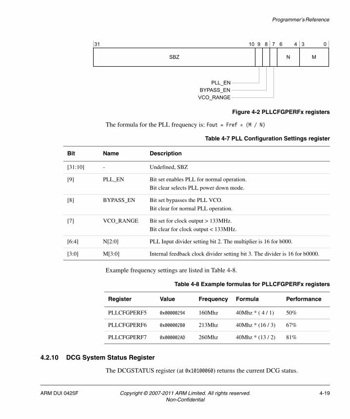
Programmer’s Reference
Figure 4-2 PLLCFGPERFx registers
The formula for the PLL frequency is: Fout = Fref * (M / N)
Example frequency settings are listed in Table 4-8.
4.2.10 DCG System Status Register
The DCGSTATUS register (at 0x10100060) returns the current DCG status.
SBZ
31 10 9 8 7 6 4 3 0
N M
PLL_ENBYPASS_EN
VCO_RANGE
Table 4-7 PLL Configuration Settings register
Bit Name Description
[31:10] - Undefined, SBZ
[9] PLL_EN Bit set enables PLL for normal operation.
Bit clear selects PLL power down mode.
[8] BYPASS_EN Bit set bypasses the PLL VCO.
Bit clear for normal PLL operation.
[7] VCO_RANGE Bit set for clock output > 133MHz.
Bit clear for clock output < 133MHz.
[6:4] N[2:0] PLL Input divider setting bit 2. The multiplier is 16 for b000.
[3:0] M[3:0] Internal feedback clock divider setting bit 3. The divider is 16 for b0000.
Table 4-8 Example formulas for PLLCFGPERFx registers
Register Value Frequency Formula Performance
PLLCFGPERF5 0x00000294 160Mhz 40Mhz * ( 4 / 1) 50%
PLLCFGPERF6 0x000002B0 213Mhz 40Mhz * (16 / 3) 67%
PLLCFGPERF7 0x000002AD 260Mhz 40Mhz * (13 / 2) 81%
ARM DUI 0425F Copyright © 2007-2011 ARM Limited. All rights reserved. 4-19Non-Confidential
Programmer’s Reference
Note Reading 0x10100060 returns the DCG status and writing sets the AXI priority.
4.2.11 AXI Priority Register
The AXIPRIORITY register (at 0x10100060) sets the 64-bit AXI arbitration priority.
Table 4-9 AXIPriority register
Bit Name Description
[31:23] - Undefined, SBZ
[22:20] AXIPRIORITY CAI lowest priority slave interface.
Reset value is b101.
[19] - Undefined, SBZ
[18:16] - CAI next highest priority slave interface.
Reset value is b100.
[15] - Undefined, SBZ
[14:12] - CAI next highest priority slave interface.
Reset value is b011.
[11] - Undefined, SBZ
[10:8] - CAI next highest priority slave interface.
Reset value is b010.
[7] - Undefined, SBZ
[6:4] - CAI next highest priority slave interface.
Reset value is b001.
[3] - Undefined, SBZ
[2:0] - CAI highest priority slave interface.
Reset value is b000.
4-20 Copyright © 2007-2011 ARM Limited. All rights reserved. ARM DUI 0425FNon-Confidential
Programmer’s Reference
4.2.12 SMC Exclusive Access Monitor ID Register
The SMCEXTACMONID register (at 0x10100064) returns the static memory controller exclusive access monitor ID value.
4.2.13 DLL Calibrate Register
The read-only DLL Calibrate register (at 0x10100068) returns the DLL update period.
Table 4-10 SMC Exclusive Access Monitor ID register
Bit Name Description
[31:14] - Undefined, SBZ
[13:8] SMCEXACMONID SMC Exclusive Access Monitor ID 1
[7:6] - Undefined, SBZ
[5:0] - SMC Exclusive Access Monitor ID 0
Table 4-11 DLL Calibrate Outputs register
Bit Name Description
[31:8] - Undefined, SBZ
[7:0] DLLCALIBRATE DLL calibrate settings
ARM DUI 0425F Copyright © 2007-2011 ARM Limited. All rights reserved. 4-21Non-Confidential

Programmer’s Reference
4.3 Advanced Power Controller and Power Management Interface
Control and monitoring of the ARM1176JZF-S development chip voltages are provided by the Advanced Power Controller and the Power Management Interface:
• The interface to the Advanced Power Controller is provided by the APC registers in the development chip. The IEM performance level controller can send commands to the APC to control the voltages supplied to the development chip.
Note The APC requires a separate license for the controller and the documentation on
the controller registers. Contact ARM for more information on licensing the APC component and obtaining the documentation required to use the APC with the IEM subsystem.
• The Power Management Interface is a custom peripheral in the FPGA that extends the IEM capabilities of the development chip. It is used as a basic data logger for recording voltage, current, power levels for the development chip and SDRAM.
Note For details of the other IEM subsystem components, see:
• ARM1176JZF-S development chip system controller on page 4-12
• Intelligent Energy Management on page 3-15.
Table 4-12 Power Management Interface and IEM Interface implementation
Property Value
Location IEM controller in development chip and power monitoring registers in FPGA.
Memory base address 0x1001C000 for PMI in FPGA
0x10102000 for APC in development chip.
Interrupt -
Release version PMI and APC are custom implementations.
Reference documentation Power Management Interface registers in the FPGA on page 4-23.
4-22 Copyright © 2007-2011 ARM Limited. All rights reserved. ARM DUI 0425FNon-Confidential

Programmer’s Reference
4.3.1 Power Management Interface registers in the FPGA
The Power Management Interface consists of the memory locations and registers listed in Table 4-13. All registers except PWR_CONTROL are read-only.
Table 4-13 Power Management Interface registers in the FPGA
Register Address Description
PWR_CONTROL 0x1001C000 Enables RAM recording of voltage, current, and power.
PWR_VOLTAGE_CTL0 0x1001C010 Present VDDCORE reading
PWR_VOLTAGE_CTL1 0x1001C014 Present VSOC reading
PWR_VOLTAGE_CTL2 0x1001C018 Present VDDRAM reading
PWR_VOLTAGE_CTL3 0x1001C01C Present TPSENSE reading
PWR_VOLTAGE_CTL4 0x1001C020 Present PWROK reading
PWR_VOLTAGE_AVG0 0x1001C030 Average of VDDCORE over last 1024 readings
PWR_VOLTAGE_AVG1 0x1001C034 Average of VSOC over last 1024 readings
PWR_VOLTAGE_AVG2 0x1001C038 Average of VDDRAM over last 1024 readings
PWR_VOLTAGE_AVG3 0x1001C03C Average of TPSENSE over last 1024 readings
PWR_MEMA 0x1001C800–0x1001C8FF Last 512 IEM memreq and corereqs
PWR_MEMB 0x1001C900–0x1001C9FF Last 512 VDDCORE readings
PWR_MEMC 0x1001CA00–0x1001CAFF Last 512 VDDCORE power readings
PWR_MEMD 0x1001CB00–0x1001CBFF Last 512 VSOC readings
PWR_MEME 0x1001CC00–0x1001CEFF Last 512 VSOC power readings
PWR_MEMF 0x1001CD00–0x1001CDFF Last 512 VDDRAM readings
PWR_MEMG 0x1001CE00–0x1001CEFF Last 512 VDDRAM power readings
APC control 0x10102000–0x10102FFF Reserved
ARM DUI 0425F Copyright © 2007-2011 ARM Limited. All rights reserved. 4-23Non-Confidential

Programmer’s Reference
PWR_CONTROL
Setting the RAM Enable bit to 0 stops more data being recorded to the memories. This enables software to fix the history buffers for software analysis.
PWR_VOLTAGE_CTLx
Read the voltage and current for the supplies listed in Table 4-15:
Note The reading from the register is relative and must be converted to an absolute value by the formula:
Voltage = (PWR_VOLTAGE_CTLx *18) / 655200
Table 4-14 PWR_CONTROL
Bits Access Description
[31:1] - Reserved. Use read-modify-write to preserve value.
[0] Read/write Enables cyclic recording of data to mem areas. (power-on reset state is 1)
Table 4-15 PWR_READx registers
Register Address Description
PWR_VOLTAGE_CTL0 0x10010010 Present VDDCORE reading
PWR_VOLTAGE_CTL1 0x10010014 Present VSOC reading
PWR_VOLTAGE_CTL2 0x10010018 Present VDDRAM reading
PWR_VOLTAGE_CTL3 0x1001001C Present TPSENSE reading
PWR_VOLTAGE_CTL4 0x10010020 Present PWROK reading
Table 4-16 PWR_READx content
Bits Access Description
[31:16] Read only Present current level (or TPSENSA voltage if PWR_VOLTAGE_CTL3)
[15:0] Read only Present voltage level (or TPSENSB voltage if PWR_VOLTAGE_CTL3)
4-24 Copyright © 2007-2011 ARM Limited. All rights reserved. ARM DUI 0425FNon-Confidential

Programmer’s Reference
PWR_VOLTAGE_AVGx
Read the average voltage and current for the supplies listed in Table 4-15 on page 4-24:
Note The reading from the register is relative and must be converted to an absolute value by the formula:
Voltage = (PWR_VOLTAGE_AVGx *18) / 655200
PWR_MEMx
There are seven 512x32bit block RAMs embedded into the power monitor that enable reading the last 512 values. It also records the relative power consumed (voltage * current). This enables very fast software analysis of historical power use.
Table 4-17 PWR_AVGx registers
Register Address Description
PWR_VOLTAGE_AVG0 0x10010030 Average of VDDCORE over last 1024 readings
PWR_VOLTAGE_AVG1 0x10010034 Average of VSOC over last 1024 readings
PWR_VOLTAGE_AVG2 0x10010038 Average of VDDRAM over last 1024 readings
PWR_VOLTAGE_AVG3 0x1001003C Average of TPSENSE over last 1024 readings
Table 4-18 PWR_AVGx content
Bits Access Description
[31:16] Read only Read average current level (or TPSENSA voltage if PWR_VOLTAGE_AVG3)
[15:0] Read only Read average voltage level (or TPSENSB voltage if PWR_VOLTAGE_AVG3)
ARM DUI 0425F Copyright © 2007-2011 ARM Limited. All rights reserved. 4-25Non-Confidential

Programmer’s Reference
The RAM at 0x1001C800 records the history of requests from the PowerWise Interface. This enables the additional comparison of historical power use against requests from the IEM (and consequently the correlation between the two). See Table 4-15 on page 4-24:
Note The reading from the register is relative and must be converted to an absolute value by Voltage = (PWR_MEMx *18) / 655200
Table 4-19 PWR_MEMx registers
Register Address Description
PWR_MEMA 0x1001C800–
0x1001CFFF
Requests from the PowerWise Interface
PWR_MEMB 0x1001D000–
0x1001D7FF
Last 512 VDDCORE readings
PWR_MEMC 0x1001D800–
0x1001DFFF
Last 512 VDDCORE power readings
PWR_MEMD 0x1001E000–
0x1001E7FF
Last 512 VSOC readings
PWR_MEME 0x1001E800–
0x1001EFFF
Last 512 VSOC power readings
PWR_MEMF 0x1001F000–
0x1001F7FF
Last 512 VDDRAM readings
PWR_MEMG 0x1001F800–
0x1001FFFF
Last 512 VDDRAM power readings
Table 4-20 PWR_MEMx content
Bits Access Description
[31:16] Read only Reserved.
[15:0] Read only Voltage or power level
4-26 Copyright © 2007-2011 ARM Limited. All rights reserved. ARM DUI 0425FNon-Confidential

Programmer’s Reference
4.4 Advanced Audio CODEC Interface, AACI
The PrimeCell Advanced Audio CODEC Interface (AACI) is an AMBA compliant SoC peripheral that is developed, tested, and licensed by ARM Limited.
4.4.1 PrimeCell Modifications
The AACI PrimeCell in the PB1176JZF-S has a different FIFO depth than the standard PL041. Therefore, the AACIPeriphID3 register contains the values listed in Table 4-22 on page 4-28.
Figure 4-3 AACI ID register
Table 4-21 AACI implementation
Property Value
Location FPGA (the CODEC is an external LM4549)
Memory base address 0x10004000
Interrupt 41 on FPGA GICs
Release version ARM AACI PL041 r1p0 (modified to one channel and 256 FIFO depth in compact mode and 512 in non-compact mode)
Reference documentation ARM PrimeCell Advanced Audio CODEC Interface (PL041) Technical Reference Manual and National Semiconductor LM4549 Data Sheet. (See also changed PrimeCell ID listed in Table 4-22 on page 4-28 and Advanced Audio Codec Interface, AACI on page 3-24. on page 3-24)
ARM DUI 0425F Copyright © 2007-2011 ARM Limited. All rights reserved. 4-27Non-Confidential
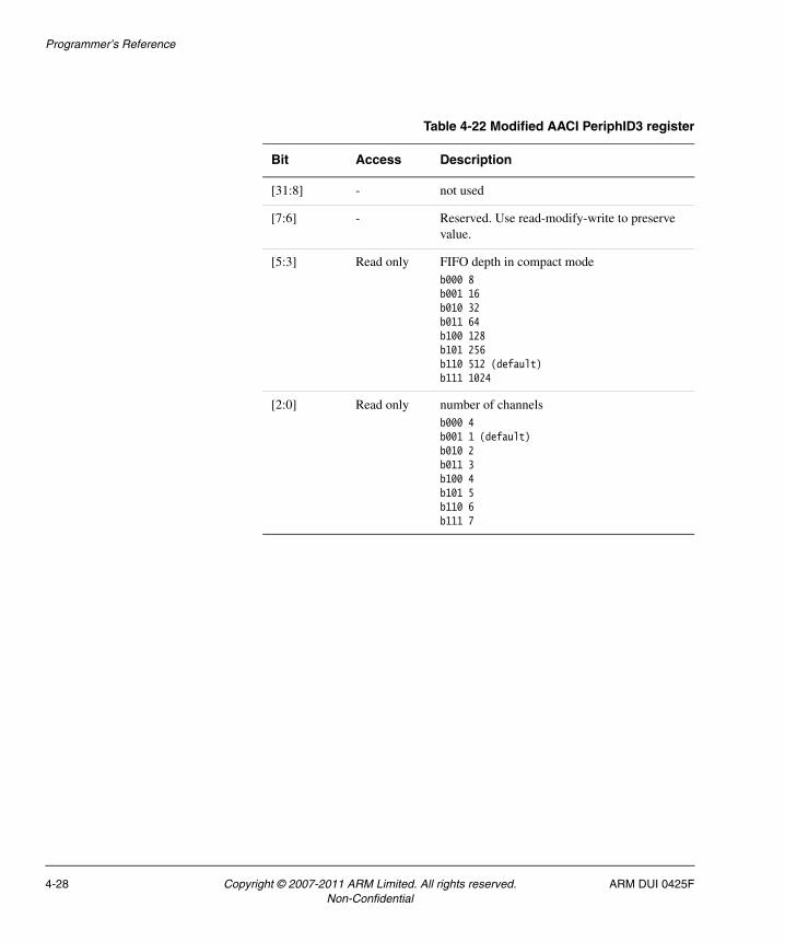
Programmer’s Reference
Table 4-22 Modified AACI PeriphID3 register
Bit Access Description
[31:8] - not used
[7:6] - Reserved. Use read-modify-write to preserve value.
[5:3] Read only FIFO depth in compact modeb000 8b001 16b010 32b011 64b100 128b101 256b110 512 (default)b111 1024
[2:0] Read only number of channelsb000 4b001 1 (default)b010 2b011 3b100 4b101 5b110 6b111 7
4-28 Copyright © 2007-2011 ARM Limited. All rights reserved. ARM DUI 0425FNon-Confidential

Programmer’s Reference
4.5 Character LCD display
This is a custom peripheral that provides an interface to a standard HD44780 16 x 2 character LCD module.
Note The HD44780 display interface is very slow.
Requests to read or write data or a command to the character LCD are captured and executed later. It is not until 500ns later that the access is completed. Poll access complete flag (bit 0 of CHAR_RAW) or wait for a Char LCD interrupt on SIC7 to check that the last access has completed.
After accepting a command, the character LCD typically requires 37μs to finish processing. Some commands, Return Home for example, take substantially longer (20ms). Poll the busy signal to determine when the display is ready for a new data or command write.
An interrupt signal is generated by the character LCD controller a short time after the raw data is valid. However this interrupt signal is reserved for future use and you must use a polling routine instead of an interrupt service routine.
Table 4-23 Character LCD display implementation
Property Value
Location FPGA
Memory base address 0x10008000
Interrupt 39 on FPGA GICs
Release version Custom logic
Reference documentation datasheet for the Hitachi HD44780 display (see also Character LCD controller on page 3-24)
ARM DUI 0425F Copyright © 2007-2011 ARM Limited. All rights reserved. 4-29Non-Confidential

Programmer’s Reference
The control and data registers for the character LCD interface are listed in Table 4-24.
Table 4-24 Character LCD control and data registers
Address Name Type Description
0x10008000 CHAR_COM Write command, read busy status
A write to this address causes a write to the HD44780 command register some cycles later.A read from this address causes a read from the HD44780 busy register some cycles later.
Note The data read from this address is not valid LCD register data. Use the CHAR_RAW and CHAR_RD registers to return LCD register data.
0x10008004 CHAR_DAT Write data RAM, read data RAM
A write to this address causes a write to the HD44780 data register some cycles later.A read to this address causes a read to the HD44780 data register some cycles later. The data read from this address is not valid LCD register data. Use the CHAR_RAW and CHAR_RD registers to return LCD register data.
0x10008008 CHAR_RD Read captured data from an earlier read command
Bits [7:0] contain the data from last request read, valid only when bit 0 is set in CHAR_RAW. Bits [31:8] must be ignored.
0x1000800C CHAR_RAW Write to reset access complete flag, read to determine if data in CHAR_RD is valid
Bit 8 indicates AccessComplete (write 0 to clear). The bit is set if read data is valid. Bits [31:9] and [7:0] must be ignored.
0x10008010 CHAR_MASK Write interrupt mask Set bit 0 to 1 to enable AccessComplete to generate an interrupt on SIC 7.
0x10008014 CHAR_STAT Read status Bit 0 is the state of AccessComplete ANDed with the CHAR_MASK
4-30 Copyright © 2007-2011 ARM Limited. All rights reserved. ARM DUI 0425FNon-Confidential

Programmer’s Reference
An overview of the commands available is listed in Table 4-25.
For more details on the character display, see the Hitachi HD44780 datasheet. Example code for accessing the character LCD is provided on the CD as part of the Boot Monitor and Selftest applications. This code is copied to your hard disk during installation, see:
• install_dir\software\firmware\Platform\source\lcd_dbg.c
• install_dir\software\projects\selftest\apcharlcd\apcharldc.c.
Table 4-25 Character LCD display commands
Command Bit pattern
Description
Clear display b00000001 Clears entire display and sets display RAM address counter to zero.
Return home b0000001x Sets display RAM address counter to zero and returns the cursor to the first character position. Display RAM contents are not erased.
Entry mode set b000001DS Sets cursor move direction to increment (D HIGH) or decrement (D LOW).
Specifies display shift (S HIGH).
This setting affects future display RAM read or write operation.
Display on/off control
b00001DCB Sets entire display on /off (D HIGH for on)
Sets cursor on/off (C HIGH for on)
Sets cursor position character blinking on/off (B HIGH for on).
Cursor or display shift
b0001CDxx Moves cursor (C LOW) or shifts display (C HIGH) right (D HIGH) or left (D LOW) without changing display RAM contents.
Function set b001LNFxx Sets interface data length to 8 (L HIGH, the default) or 4 (L LOW).
Sets number of display lines to two (N HIGH, the default) or Sets one (N LOW).
Sets character font to 5x10 (F HIGH, the default) or 5x8 (F LOW).
Set CGRAM address
b01AAAAAA Sets character generator RAM address to bAAAAAA. Character generator RAM data is sent and received after this setting.
Set DDRAM address
b1AAAAAAA Sets display RAM address to bAAAAAAA. Display RAM data is sent and received after this setting.
ARM DUI 0425F Copyright © 2007-2011 ARM Limited. All rights reserved. 4-31Non-Confidential

Programmer’s Reference
4.6 Color LCD Controller, CLCDC
The PrimeCell Color LCD Controller (CLCDC) is an AMBA compliant SoC peripheral that is developed, tested, and licensed by ARM Limited.
The following locations are reserved, and must not be used during normal operation:
• locations at offsets 0x030 to 0x1FE are reserved for possible future extensions
• locations at offsets 0x400 to 0x7FF are reserved for test purposes.
Table 4-26 CLCDC implementation
Property Value
Location ARM1176JZF-S development chip
Memory base address 0x10112000
Interrupt 47 on development chip GIC
(15 on TZIC)
Release version ARM CLCDC PL111 r0p0-00alp0 (extended to include the hardware cursor from ARM CLCDC PL110 r0p0)
Reference documentation ARM PrimeCell Color LCD Controller (PL111) Technical Reference Manual For details on the hardware cursor registers, see the ARM926EJ-S Technical Reference Manual. See also address modifications listed in PrimeCell Modifications on page 4-33, Display resolutions and display memory organization on page 4-33, and CLCDC interface on page 3-18)
4-32 Copyright © 2007-2011 ARM Limited. All rights reserved. ARM DUI 0425FNon-Confidential

Programmer’s Reference
4.6.1 PrimeCell Modifications
The register map for the variant of the PL111 used in the ARM1176JZF-S development chip is not the same as the obsolete PL110. The differences are listed in Table 4-27.
4.6.2 Display resolutions and display memory organization
Different display resolutions require different data and synchronization timing. Use registers CLCD_TIM0, CLCD_TIM1, CLCD_TIM2, and SYS_OSCCLK0 to define the display timings as listed in Table 4-28.
Note The mapping of the 32 bits of pixel data in memory to the RGB display signals depends on the resolution and display mode. Resolutions based on 16 bits per pixel encode two pixels in one 32-bit word.
Table 4-27 PrimeCell CLCDC register differences
Address (Dev. Chip)
Reset value (Dev. Chip)
Description in PL110 TRM
Difference
0x10110018 0x0 LCDControl, LCD panel pixel parameters
CLCDC TRM lists address as 0x1011001C
0x1011001C 0x0 LCDIMSC, interrupt mask set and clear
CLCDC TRM lists address as 0x10110018
0x10110800–
0x10110C2C
0x0 Not present Hardware cursor registers from PL111 (see the ARM926EJ-S Technical Reference Manual for details)
0x10110FE0 0x11 CLCDPeriphID0 CLCDC TRM lists value as 0x10
0x10110FE4 0x11 CLCDPeriphID1 CLCDC TRM lists value as 0x11
Table 4-28 Values for different display resolutions
Display resolutionCLCDCLK frequency and SYS_OSCCLK0 register value
CLCD_TIM0 register at 0x10112000
CLCD_TIM1 register 0x10112004
CLCD_TIM2 register at 0x10112008
VGA (640x480) on VGA 25MHz, 0x35C57 0x3F0F4F9C 0x0D030DDF 0x067F3800
SVGA (800x600) on SVGA 36MHz, 0x35C91 0x6F1F4FC4 0x11030E57 0x071F3800
XVGA(1024x768) on XVGA 64MHz, 0x35CF6 0x972F67FC 0x17030EFF 0x07FF3800
ARM DUI 0425F Copyright © 2007-2011 ARM Limited. All rights reserved. 4-33Non-Confidential

Programmer’s Reference
4.7 Dynamic Memory Controller, DMC
The Dynamic Memory Controller (DMC) is an AMBA compliant SoC peripheral that is developed, tested, and licensed by ARM Limited.
The DMC controls the dynamic memory on the PB1176JZF-S.
4.7.1 Register values
Table 4-30 lists the register values for typical operation with 133MHz SDRAM. The HCLK frequency is 105MHz and the SDRAM is organized as four banks of 8MB x 16bit.
Note The platform.a library contains memory setup routines. See Appendix F Boot Monitor and platform library.
Table 4-29 DMC implementation
Property Value
Location ARM1176JZF-S development chip
Memory base address 0x10109000 (for configuration)
Interrupt NA
Release version ARM DMC PL340
Reference documentation ARM PrimeCell Dynamic Memory Controller (PL340) Technical Reference Manual (see also Memory interface on page 3-17)
Table 4-30 SDRAM register values
Address Register name Access Value Description
0x10109000 DMC_memc_status Read/write - -
0x10109004 DMC_memc_cmd Write only - -
0x10109008 DMC_direct_cmd Write only - -
0x1010900C DMC_memory_cfg Read/write 0x19112 -
4-34 Copyright © 2007-2011 ARM Limited. All rights reserved. ARM DUI 0425FNon-Confidential

Programmer’s Reference
0x10109010 DMC_refresh_prd Read/write 0x01C2 -
0x10109014 DMC_cas_latency Read/write 0x0006 -
0x10109018 DMC_t_dqss Read/write 0x0001 -
0x1010901C DMC_t_mrd Read/write 0x0002 -
0x10109020 DMC_t_ras Read/write 0x0007 -
0x10109024 DMC_t_rc Read/write 0x0009 -
0x10109028 DMC_t_rcd Read/write 0x0003 -
0x1010902C DMC_t_rfc Read/write 0x00C9 -
0x10109030 DMC_t_rp Read/write 0x0003 -
0x10109034 DMC_t_rrd Read/write 0x0002 -
0x10109038 DMC_t_wt Read/write 0x0002 -
0x1010903C DMC_t_wtr Read/write 0x0001 -
0x10109040 DMC_t_xp Read/write 0x0003 -
0x10109044 DMC_t_xsr Read/write 0x000F -
0x10109048 DMC_t_esr Read/write 0x0014 -
0x10109100 DMC_id_n_ncfg Read/write 0x0 -
0x10109200 DMC_chip_n_ncfg Read/write 0x00F8 -
0x10109300 DMC_user_status Read only - -
0x10109304 DMC_user_config Write only - -
0x10109FE0 DMC_periph_id_n Read only - -
0x10109FF0 DMC_comp_id_n Read only - -
Table 4-30 SDRAM register values (continued)
Address Register name Access Value Description
ARM DUI 0425F Copyright © 2007-2011 ARM Limited. All rights reserved. 4-35Non-Confidential

Programmer’s Reference
4.8 Ethernet
The Ethernet interface is implemented in an external SMC LAN9118 10/100 Ethernet single-chip MAC and PHY. The internal registers of the LAN9118 are memory-mapped onto the AHB M2 bus and occupy 16 word locations at 0x3A000000.
To access the PHY MII registers, you must implement a synchronous serial connection in software to control the management register in Bank 3. By default, the PHY is set to isolate in the control register. This disables the external interface. See the LAN91C111 application note or to the self test program supplied on the CD for additional information.
When manufactured, an ARM value for the Ethernet MAC address and the register base address are loaded into the EEPROM. The register base address is 0. The MAC address is unique, but can be reprogrammed if required. Reprogramming of the EEPROM is done through Bank 1 (general and control registers).
Table 4-31 Ethernet implementation
Property Value
Location Board (LAN9118 chip)
Memory base address 0x3A000000 on SMC CS 6
Interrupt 42 on FPGA GICs
Release version The FPGA contains a custom interface to the LAN9118 chip
Reference documentation LAN9118 Data Sheet (see also Ethernet interface on page 3-29).
4-36 Copyright © 2007-2011 ARM Limited. All rights reserved. ARM DUI 0425FNon-Confidential

Programmer’s Reference
4.9 FPGA status and system control registers
The PB1176JZF-S status and system control registers enable the processor to determine its environment and to control some on-board operations. The registers, listed in Table 4-32, are located from 0x10000000.
See also Reset controller on page 3-32 for a description of the reset logic.
Note All registers are 32 bits wide and do not support byte writes. Write operations must be word-wide. Bits marked as reserved in the following sections must be preserved using read-modify-write operations.
In Table 4-32, the entry for Reset Level indicates the highest reset level that modifies its contents:
Level 1 Pressing the FPGA CONFIG initiates reconfiguration of the FPGA. Registers that have a reset level of 0 are not affected.
Level 0 The system power on reset (nSYSPOR) is a level 0 reset and initializes all registers to their default value. This level reset also resets all registers that have reset level of 1.
Table 4-32 Register map for FPGA System Controller registers
Name Address Accessa Reset level
Description
SYS_ID 0x10000000 Read only - System Identity. See ID Register, SYS_ID on page 4-40.
SYS_SW 0x10000004 Read only - Bits [7:0] map to S6 (user switches)
SYS_LED 0x10000008 Read/Write 1 Bits [7:0] map to user LEDs (located next to S6)
SYS_OSC0 0x1000000C Read/Write Lockable
1 Settings for the ICS307 programmable oscillator chip OSC0. This oscillator provides the CLCDCLKEXT signal source. See Oscillator registers, SYS_OSCx on page 4-42 and ARM1176JZF-S development chip clocks on page 3-40.
SYS_OSC1 0x10000010 Read/Write Lockable
1 Settings for the ICS307 programmable oscillator chip OSC1. This oscillator provides the signal source PLLREFCLK1.
ARM DUI 0425F Copyright © 2007-2011 ARM Limited. All rights reserved. 4-37Non-Confidential

Programmer’s Reference
SYS_OSC2 0x10000014 Read/Write Lockable
1 Settings for the ICS307 programmable oscillator chip OSC2. This oscillator provides the reference to the AXI bus multiplexer and the signal source PLLREFCLK2.
SYS_OSC3 0x10000018 Read/Write Lockable
1 Settings for the ICS307 programmable oscillator chip OSC3. This oscillator provides the signal source PLLREFCLK.
SYS_OSC4 0x1000001C Read/Write Lockable
1 Settings for the ICS307 programmable oscillator chip OSC4. This clock is not used.
SYS_LOCK 0x10000020 Read/Write 1 Write 0xA05F to unlock. See Lock Register, SYS_LOCK on page 4-43.
SYS_100HZ 0x10000024 Read only 0 100Hz counter.
SYS_CFGDATA1 0x10000028 Read/Write Lockable
0 Configuration data to be applied to HDATAM1 pins at power on or when the SDC CONFIG pushbutton is pressed.
SYS_CFGDATA2 0x1000002C Read/Write Lockable
0 Configuration data to be applied to HDATAM2 pins at power on or when the SDC CONFIG pushbutton is pressed.
SYS_FLAGS 0x10000030 Read only 1 General-purpose flags (reset by any reset). See Flag registers, SYS_FLAGx and SYS_NVFLAGx on page 4-48.
SYS_FLAGSSET 0x10000030 Write 1 Set bits in general-purpose flags.
SYS_FLAGSCLR 0x10000034 Write 1 Clear bits in general-purpose flags.
SYS_NVFLAGS 0x10000038 Read only 0 General-purpose nonvolatile flags (reset only on power up).
SYS_NVFLAGSSET 0x10000038 Write 0 Set bits in general-purpose nonvolatile flags.
SYS_NVFLAGSCLR 0x1000003C Write 0 Clear bits in general-purpose nonvolatile flags.
SYS_RESETCTL 0x10000040 Read/Write Lockable
0 The reset control register sets reset depth and programmable soft reset.
SYS_PCICTL 0x10000044 Read only - Read returns a HIGH in bit [0] if a PCI board is present in the expansion backplane.
Table 4-32 Register map for FPGA System Controller registers (continued)
Name Address Accessa Reset level
Description
4-38 Copyright © 2007-2011 ARM Limited. All rights reserved. ARM DUI 0425FNon-Confidential

Programmer’s Reference
Reserved 0x10000048 Read only - Was SYS_MCI on PB926.
SYS_FLASH 0x1000004C Read/Write 1 Controls write protection of flash devices.
SYS_CLCD 0x10000050 Read/Write 1 Controls LCD power and multiplexing.
Reserved 0x10000054 Read/Write 1 -
SYS_BOOTCS 0x10000058 Read only - Contains the settings of the boot switch S1.
SYS_24MHz 0x1000005C Read only 1 32-bit counter clocked at 24MHz.
SYS_MISC 0x10000060 Read only 1 See Miscellaneous System Control Register, SYS_MISC on page 4-52 for details.
SYS_BUSID 0x10000080 Read/only 1 Shows the BUSID of transaction, indicates master no.
See Bus status registers, SYS_BUSID on page 4-53.
SYS_PROCID1 0x10000084 Read/only 1 Shows that the primary processor is an ARM11
See System status registers, SYS_PROCIDx on page 4-54.
SYS_PROCID2 0x10000088 Read/only 1 Shows that there is no directly connected Core Tile.
See System status registers, SYS_PROCIDx on page 4-54.
SYS_OSCRESET0 0x1000008C Read/Write Lockable
0 Value to load into the SYS_OSC0 register if the DEV CHIP RECONFIGURE pushbutton is pressed (APPLYCFGWORD active).
At power-on reset, the SYS_OSCRESET0 is loaded with the same default value as used for SYS_OSC0.
SYS_OSCRESET1 0x10000090 Read/Write Lockable
0 Value to load into the SYS_OSC1 register if the DEV CHIP RECONFIGURE pushbutton is pressed (APPLYCFGWORD active).
At power-on reset, the SYS_OSCRESET1 is loaded with the same default value as used for SYS_OSC1.
SYS_OSCRESET2 0x10000094 Read/Write Lockable
0 Value to load into the SYS_OSC2 register if the DEV CHIP RECONFIGURE pushbutton is pressed (APPLYCFGWORD active).
At power-on reset, the SYS_OSCRESET2 is loaded with the same default value as used for SYS_OSC2.
Table 4-32 Register map for FPGA System Controller registers (continued)
Name Address Accessa Reset level
Description
ARM DUI 0425F Copyright © 2007-2011 ARM Limited. All rights reserved. 4-39Non-Confidential

Programmer’s Reference
4.9.1 ID Register, SYS_ID
The SYS_ID register at 0x10000000 is a read-only register that identifies the board manufacturer, board type, and revision. Figure 4-4 shows the bit assignment of the register.
Figure 4-4 ID Register, SYS_ID
SYS_OSCRESET3 0x10000098 Read/Write Lockable
0 Value to load into the SYS_OSC3 register if the DEV CHIP RECONFIGURE pushbutton is pressed (APPLYCFGWORD active).
At power-on reset, the SYS_OSCRESET3 is loaded with the same default value as used for SYS_OSC3.
SYS_OSCRESET4 0x1000009C Read/Write Lockable
0 Value to load into the SYS_OSC4 register if the DEV CHIP RECONFIGURE pushbutton is pressed (APPLYCFGWORD active).
At power-on reset, the SYS_OSCRESET4 is loaded with the same default value as used for SYS_OSC4.
SYS_TEST_OSC0 0x100000C0 Read only 1 32-bit counter clocked from ISC307 clock 0.
SYS_TEST_OSC1 0x100000C4 Read only 1 32-bit counter clocked from ISC307 clock 1.
SYS_TEST_OSC2 0x100000C8 Read only 1 32-bit counter clocked from ISC307 clock 2.
SYS_TEST_OSC3 0x100000CC Read only 1 32-bit counter clocked from ISC307 clock 3.
SYS_TEST_OSC4 0x100000D0 Read only 1 32-bit counter clocked from ISC307 clock 4.
a. If Access is lockable, the register can only be written if SYS_LOCK is unlocked (see Lock Register, SYS_LOCK on page 4-43).
Table 4-32 Register map for FPGA System Controller registers (continued)
Name Address Accessa Reset level
Description
BOARD VAR ARCH
831 28 27 16 15 12 11 7
REV
0
FPGA
4-40 Copyright © 2007-2011 ARM Limited. All rights reserved. ARM DUI 0425FNon-Confidential

Programmer’s Reference
Table 4-33 describes the PB1176JZF-S ID Register assignment.
4.9.2 Switch Register, SYS_SW
Use the SYS_SW register at 0x10000004 to read the general purpose (user) switch S6. A value of 1 indicates that the switch is on.
Figure 4-5 SYS_SW
4.9.3 LED Register, SYS_LED
Use the SYS_LED register at 0x10000008 to set the user LEDs. (The LEDs are located next to user switch S6.) Set the corresponding bit to 1 to illuminate the LED.
Figure 4-6 SYS_LED
Table 4-33 ID Register, SYS_ID bit assignment
Bits Access Name Description
[31:28] Read REV FPGA revision: 0 = A, F=ALL
[27:16] Read BOARD HBI board design: 0x147 = HBI-0147
[15:12] Read VAR System variant: 0 = A, F=ALL
[11:8] Read ARCH Architecture: 5=Multi-layer AXI
[7:0] Read FPGA FPGA build number
ARM DUI 0425F Copyright © 2007-2011 ARM Limited. All rights reserved. 4-41Non-Confidential

Programmer’s Reference
4.9.4 Oscillator registers, SYS_OSCx
The oscillator registers, SYS_OSC0 to SYS_OSC4 at 0x1000000C–0x1000001C, are read/write registers that control the frequency of the clocks generated by the ICS307 programmable oscillators. A serial interface transfers the values in the registers to the programmable oscillators when a reset occurs.
Note If the DEV CHIP RECONFIG pushbutton is pressed, the contents of the SYS_OSCRESETx registers are copied into the SYS_OSCx registers before the contents are transmitted to the programmable oscillators. This enables the clock frequencies and the clock divider ratios to be changed at the same time.
Figure 4-7 shows the bit assignment of the registers.
Figure 4-7 Oscillator Register, SYS_OSCx
Table 4-34 lists the details of the SYS_OSCx registers.
Table 4-34 Oscillator Register, SYS_OSCx bit assignment
Bits Access Description
[31:19] Reserved, Use read-modify-write to preserve value.
[18:16] Read/write DIVIDE[2:0], output divider select
[15:9] Read/write RDW[6:0], reference divider word
[8:0] Read/write VDW[8:0], VCO divider word
4-42 Copyright © 2007-2011 ARM Limited. All rights reserved. ARM DUI 0425FNon-Confidential

Programmer’s Reference
For more information on bit values, see ICS307 programmable clock generators on page 3-48 and Clock rate restrictions on page B-4.
Note Before writing to a SYS_OSC register, unlock it by writing the value 0x0000A05F to the SYS_LOCK register. After writing the SYS_OSC register, relock it by writing any value other than 0x0000A05F to the SYS_LOCK register.
4.9.5 Lock Register, SYS_LOCK
The SYS_LOCK register at 0x10000020 locks or unlocks access to the following registers:
• Oscillator registers, SYS_OSCx
• Reset values for oscillators, SYS_OSCRESETx.
• Configuration registers, SYS_CFGDATAx
• Reset control register, SYS_RESETCTL
The control registers cannot be modified while they are locked. This mechanism prevents the registers from being overwritten accidently. The registers are locked by default after a reset. Figure 4-8 shows the bit assignment of the register.
Figure 4-8 Lock Register, SYS_LOCK
Table 4-35 Default values for oscillators
Address Signal Default value Reference for
0x1000000C OSC_CLK[0] 0x00002C8E CLCDCLKEXT
0x10000010 OSC_CLK[1] 0x00002CA7 PLLREFCLK1
0x10000014 OSC_CLK[2] 0x00002CA7 PLLREFCLK2
0x10000018 OSC_CLK[3] 0x00002CA7 PLLREFCLK
0x1000001C OSC_CLK[4] 0x00002C2A not used
ARM DUI 0425F Copyright © 2007-2011 ARM Limited. All rights reserved. 4-43Non-Confidential
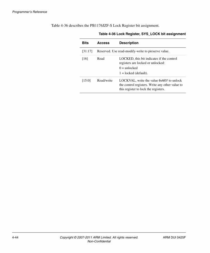
Programmer’s Reference
Table 4-36 describes the PB1176JZF-S Lock Register bit assignment.
Table 4-36 Lock Register, SYS_LOCK bit assignment
Bits Access Description
[31:17] Reserved. Use read-modify-write to preserve value.
[16] Read LOCKED, this bit indicates if the control registers are locked or unlocked:
0 = unlocked
1 = locked (default).
[15:0] Read/write LOCKVAL, write the value 0xA05F to unlock the control registers. Write any other value to this register to lock the registers.
4-44 Copyright © 2007-2011 ARM Limited. All rights reserved. ARM DUI 0425FNon-Confidential

Programmer’s Reference
4.9.6 100Hz Counter, SYS_100HZ
The SYS_100HZ register at 0x10000024 is a 32-bit counter incremented at 100Hz. The 100Hz reference is derived from the 32.768KHz crystal oscillator. The register is set to zero by a reset.
4.9.7 Configuration registers SYS_CFGDATAx
The read/write registers SYS_CFGDATA1 (at 0x10000028) and SYS_CFGDATA2 (at 0x1000002C) contain configuration data. See Table 4-37 and Table 4-38 on page 4-47 for the function associated with the register bits.
Note The values of SYS_GFGDATA1 and SYS_CFGDATA2 are loaded at reset (DEVCHIPRECONFIG) into the SoC Config registers of the processor.
In a production ASIC, the configuration signals would be tied HIGH or LOW, but they are configurable in the ARM1176JZF-S development chip. This enables you to test different build options.
Table 4-37 SYS-CFGDATA 1 register
Bits Configuration signalResetValue
Description
[31:23] Not used - Reserved for future use.
[22:21] CFGSMMWCS7[1:0] b10 SMC bank 7 data width:00 = 8-bit01 = 16-bit10 = 32-bit11 = undefined.
[20:19] CFGSMCMEMRATIO[1:0] b10 SMC AXI to external memory clock ratio:00 = 1:101 = 2:110 = 3:111 = undefined.
[18] CFGSMCAXIRATIO 0 SMC AXI sync down clock ratio:0 = 1:11 = 2:1.
ARM DUI 0425F Copyright © 2007-2011 ARM Limited. All rights reserved. 4-45Non-Confidential

Programmer’s Reference
[17:15] CFGAXIEXTRATIOMSTR[2:0] b010 AXI external master clock ratio:000 = 1:1001 = 2:1010 = 3:1011 = 4:1100 = 5:1101 = 6:1110 = 7:1111 = 8:1.
[14:12] CFGAXIEXTRATIOSLV[2:0] b010 AXI external slave clock ratio:000 = 1:1001 = 2:1010 = 3:1011 = 4:1100 = 5:1101 = 6:1110 = 7:1111 = 8:1.
[11] CFGAXIRATIO 0 AXI: Core clock ratio:0 = 2:11 = 4:1.
[10] CFGCP15SDISABLE 0 TZ write access disable
[9] CFGUBITINIT 0 ARMv6 unaligned behavior
[8] CFGBIGENDINIT 0 ARMv5 big endian behavior
[7] CFGVINITHI 0 High exception vector location
[6] CFGINITRAM 0 ITCM at 0x0 for data and instructions at reset
[5:4] CFGREMAP[1:0] b10 Defines boot memory map:00 = normal memory01 = AXI ROM10 = SMC11 = AXI master port.
[3:0] CFGCOREID[3:0] b0000 LS nibble of core ID[7:0]
Table 4-37 SYS-CFGDATA 1 register (continued)
Bits Configuration signalResetValue
Description
4-46 Copyright © 2007-2011 ARM Limited. All rights reserved. ARM DUI 0425FNon-Confidential
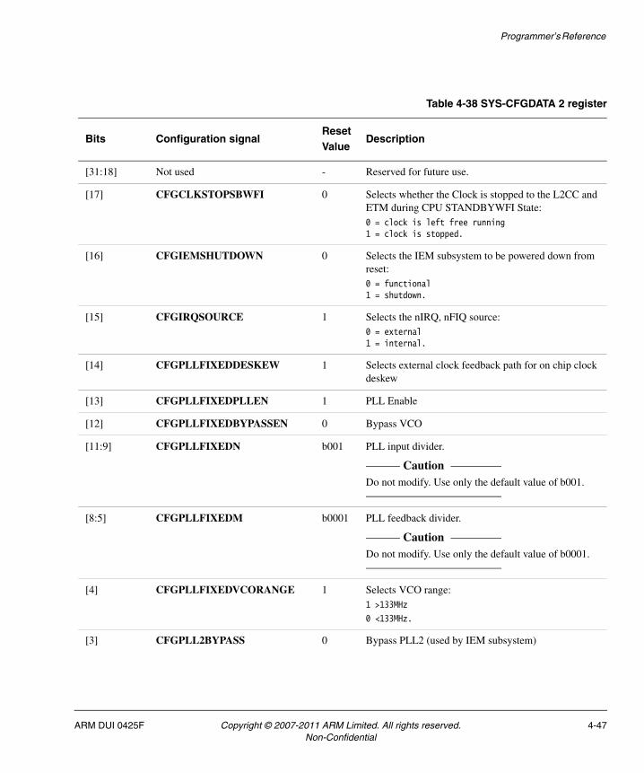
Programmer’s Reference
Table 4-38 SYS-CFGDATA 2 register
Bits Configuration signalResetValue
Description
[31:18] Not used - Reserved for future use.
[17] CFGCLKSTOPSBWFI 0 Selects whether the Clock is stopped to the L2CC and ETM during CPU STANDBYWFI State:0 = clock is left free running1 = clock is stopped.
[16] CFGIEMSHUTDOWN 0 Selects the IEM subsystem to be powered down from reset:0 = functional1 = shutdown.
[15] CFGIRQSOURCE 1 Selects the nIRQ, nFIQ source:0 = external 1 = internal.
[14] CFGPLLFIXEDDESKEW 1 Selects external clock feedback path for on chip clock deskew
[13] CFGPLLFIXEDPLLEN 1 PLL Enable
[12] CFGPLLFIXEDBYPASSEN 0 Bypass VCO
[11:9] CFGPLLFIXEDN b001 PLL input divider.
Caution Do not modify. Use only the default value of b001.
[8:5] CFGPLLFIXEDM b0001 PLL feedback divider.
Caution Do not modify. Use only the default value of b0001.
[4] CFGPLLFIXEDVCORANGE 1 Selects VCO range:1 >133MHz
0 <133MHz.
[3] CFGPLL2BYPASS 0 Bypass PLL2 (used by IEM subsystem)
ARM DUI 0425F Copyright © 2007-2011 ARM Limited. All rights reserved. 4-47Non-Confidential

Programmer’s Reference
4.9.8 Flag registers, SYS_FLAGx and SYS_NVFLAGx
The registers shown in Table 4-39 provide two 32-bit register locations containing general-purpose flags. You can assign any meaning to the flags.
The PB1176JZF-S provides two distinct types of flag registers:
• The SYS_FLAGS Register is cleared by a normal reset, such as a reset caused by pressing the reset button.
• The SYS_NVFLAGS Register retains its contents after a normal reset and is only cleared by a Power-On Reset (POR).
Flag and Nonvolatile Flag Registers
The SYS_FLAGS and SYS_NVFLAGS registers contain the current state of the flags.
[2] CFGPLL1BYPASS 0 Bypass PLL1 (used by IEM subsystem)
[1] CFGPLLBYPASS 0 Bypass PLLFIXED (typically the main reference generator, PLLREFCLK is used directly for the core clock instead of the PLL output PLLFIXEDCLK.)
[0] CFGPLLREFCLK 0 Use PLLREFCLK as the input reference for PLL1 and PLL2
Table 4-38 SYS-CFGDATA 2 register (continued)
Bits Configuration signalResetValue
Description
Table 4-39 Flag registers
Register name Address Access Reset by Description
SYS_FLAGS 0x10000030 Read Reset Flag register
SYS_FLAGSSET 0x10000030 Write Reset Flag Set register
SYS_FLAGSCLR 0x10000034 Write Reset Flag Clear register
SYS_NVFLAGS 0x10000038 Read POR Nonvolatile Flag register
SYS_NVFLAGSSET 0x10000038 Write POR Nonvolatile Flag Set register
SYS_NVFLAGSCLR 0x1000003C Write POR Nonvolatile Flag Clear register
4-48 Copyright © 2007-2011 ARM Limited. All rights reserved. ARM DUI 0425FNon-Confidential

Programmer’s Reference
Flag and Nonvolatile Flag Set Registers
The SYS_FLAGSSET and SYS_NVFLAGSSET registers are used to set bits in the SYS_FLAGS and SYS_NVFLAGS registers:
• write 1 to SET the associated flag
• write 0 to leave the associated flag unchanged.
Flag and Nonvolatile Flag Clear Registers
Use the SYS_FLAGSCLR and SYS_NVFLAGSCLR registers to clear bits in SYS_FLAGS and SYS_NVFLAGS:
• write 1 to CLEAR the associated flag
• write 0 to leave the associated flag unchanged.
4.9.9 Reset Control Register, SYS_RESETCTL
The SYS_RESETCTL register at 0x10000040 sets reset depth and programmable soft reset, see Reset controller on page 3-32 and Reset level on page 3-33. The register bits are shown in Figure 4-9 and the function of the register bits are listed in Table 4-40. You must unlock the register (see Lock Register, SYS_LOCK on page 4-43) before the register contents can be modified.
Figure 4-9 SYS_RESETCTL
Table 4-40 Reset level control
Bits Access Description
[31:9] - Reserved.
[8] Read/Write Set to 1 to force a soft reset.
[7:3] - Reserved.
[2:0] Read/Write Sets the depth of a soft reset:1=SYSRST (reset Logic Tile)2=PLLLOCK (reset PLL)4=PBRESET (board reset, same as pressing reset button)
ARM DUI 0425F Copyright © 2007-2011 ARM Limited. All rights reserved. 4-49Non-Confidential

Programmer’s Reference
4.9.10 PCI Control Register, SYS_PCICTL
The SYS_PCICTL register at 0x10000044 returns status on the PCI bus as listed in Table 4-41:
See Appendix D PCI Backplane and Enclosure, PCI controller on page 4-109, and PCI interface on page 3-27 for more information on the PCI backplane.
4.9.11 Flash Control Register, SYS_FLASH
Bit 0 of the SYS_FLASH register at 0x1000004C controls write protection of NOR flash devices. The function of the register bits are shown in Table 4-42.
4.9.12 CLCD Control Register, SYS_CLCD
The SYS_CLCD register at 0x10000050 controls LCD power and multiplexing and controls the interface to the touchscreen.
Table 4-41 PCI bus status
Bits Access Description
[31:2] Read only Reserved.
[1] Read only Reserved.
Note On the RealView Platform Baseboard for ARM926EJ-S, this bit was PCICONTROLIN signal and indicated that 66MHz mode was enabled. The PB1176JZF-S only supports 33MHz operation.
[0] Read only Status of P_DETECT pin.
Table 4-42 Flash control
Bits Access Description
[31:1] - Reserved. Use read-modify-write to preserve value.
[0] Read/write Disables writing to flash if LOW (power-on reset state is LOW)
4-50 Copyright © 2007-2011 ARM Limited. All rights reserved. ARM DUI 0425FNon-Confidential
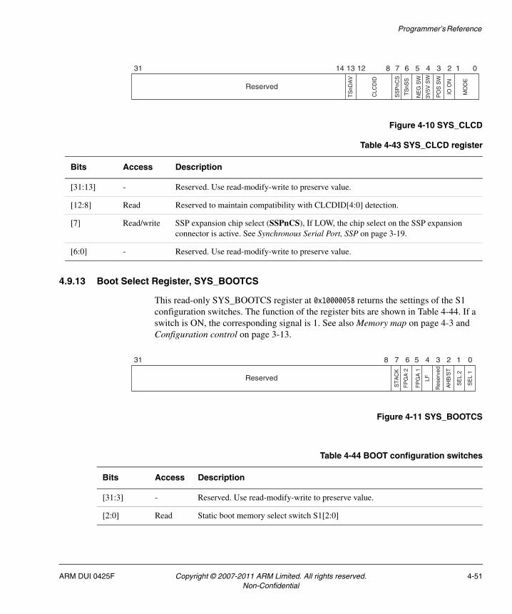
Programmer’s Reference
Figure 4-10 SYS_CLCD
4.9.13 Boot Select Register, SYS_BOOTCS
This read-only SYS_BOOTCS register at 0x10000058 returns the settings of the S1 configuration switches. The function of the register bits are shown in Table 4-44. If a switch is ON, the corresponding signal is 1. See also Memory map on page 4-3 and Configuration control on page 3-13.
Figure 4-11 SYS_BOOTCS
Table 4-43 SYS_CLCD register
Bits Access Description
[31:13] - Reserved. Use read-modify-write to preserve value.
[12:8] Read Reserved to maintain compatibility with CLCDID[4:0] detection.
[7] Read/write SSP expansion chip select (SSPnCS), If LOW, the chip select on the SSP expansion connector is active. See Synchronous Serial Port, SSP on page 3-19.
[6:0] - Reserved. Use read-modify-write to preserve value.
Table 4-44 BOOT configuration switches
Bits Access Description
[31:3] - Reserved. Use read-modify-write to preserve value.
[2:0] Read Static boot memory select switch S1[2:0]
ARM DUI 0425F Copyright © 2007-2011 ARM Limited. All rights reserved. 4-51Non-Confidential
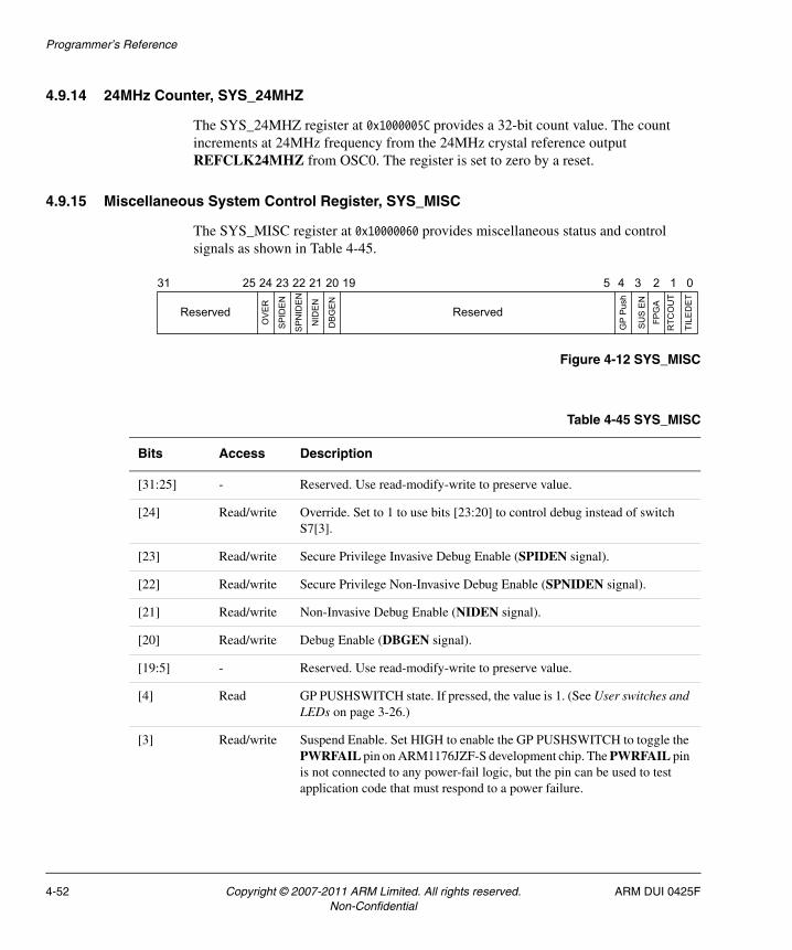
Programmer’s Reference
4.9.14 24MHz Counter, SYS_24MHZ
The SYS_24MHZ register at 0x1000005C provides a 32-bit count value. The count increments at 24MHz frequency from the 24MHz crystal reference output REFCLK24MHZ from OSC0. The register is set to zero by a reset.
4.9.15 Miscellaneous System Control Register, SYS_MISC
The SYS_MISC register at 0x10000060 provides miscellaneous status and control signals as shown in Table 4-45.
Figure 4-12 SYS_MISC
Reserved
2531 0124
TILE
DE
T
RTC
OU
TFP
GA
SU
S E
N
GP
Pus
h
324 23 22 21 20 19 5
ReservedD
BG
EN
NID
EN
SP
NID
EN
SP
IDE
N
OV
ER
Table 4-45 SYS_MISC
Bits Access Description
[31:25] - Reserved. Use read-modify-write to preserve value.
[24] Read/write Override. Set to 1 to use bits [23:20] to control debug instead of switch S7[3].
[23] Read/write Secure Privilege Invasive Debug Enable (SPIDEN signal).
[22] Read/write Secure Privilege Non-Invasive Debug Enable (SPNIDEN signal).
[21] Read/write Non-Invasive Debug Enable (NIDEN signal).
[20] Read/write Debug Enable (DBGEN signal).
[19:5] - Reserved. Use read-modify-write to preserve value.
[4] Read GP PUSHSWITCH state. If pressed, the value is 1. (See User switches and LEDs on page 3-26.)
[3] Read/write Suspend Enable. Set HIGH to enable the GP PUSHSWITCH to toggle the PWRFAIL pin on ARM1176JZF-S development chip. The PWRFAIL pin is not connected to any power-fail logic, but the pin can be used to test application code that must respond to a power failure.
4-52 Copyright © 2007-2011 ARM Limited. All rights reserved. ARM DUI 0425FNon-Confidential

Programmer’s Reference
4.9.16 Bus status registers, SYS_BUSID
The bus status register at 0x10000080 returns the ID of the bus the access was made with.
For AXI busses the AXI port used to create the read appends its own ID bits for forwarded accesses from the matrix. This value is returned on a read. This enables you to determine through software which master the software is executing on, as each bus matrix that the access passes through adds additional ID information. If the top bits are 0, then the master must be either the only master, or the primary master through any bus matrices. A non-zero value indicates that some other masters are in the system that must instead be considered the primary master.
This register returning the RID bits onto the RDATA bus. Because there is a bus matrix inside the FPGA between the HDRX bus (six ID bits), and a local master (PCI), there are usually seven ID bits in use inside the FPGA.
Although this board typically only runs software on the ARM1176JZF-S, this register is maintained to enable software compatibility with the Emulation Baseboard and to enable operating multi-core systems without the requirement to change the baseboard FPGA image.
[2] Read/write FPGA remap control (FPGA_REMAP). Default is 1.
When set to 1, AXI FPGA BOOTROM/SRAM at physical address 0x40000000 is mapped in the FPGA to address 0x00000000.
When set to 0, the ARM1176JZF-S development chip at physical address 0x00000000 is mapped in the FPGA to address 0x00000000. This allows transfers from the Logic Tile to the FPGA at address 0x00000000 to pass through the FPGA into the ARM1176JZF-S development chip SDRAM.
[1] Read RTCOUT signal from the external DS1338 real-time clock. This 32kHz signal can be used as a timer.
[0] Read nTILEDET signal. Pulled LOW if a RealView Logic Tile connects to the expansion headers.
Table 4-45 SYS_MISC (continued)
Bits Access Description
Table 4-46 SYS_BUSID
Bits Access Description
[31:7] Read only Reserved. Use read-modify-write to preserve value.
[6:0] Read only Returns bus ID.
ARM DUI 0425F Copyright © 2007-2011 ARM Limited. All rights reserved. 4-53Non-Confidential

Programmer’s Reference
4.9.17 System status registers, SYS_PROCIDx
The system status registers, SYS_PROCID1 and SYS_PROCID2, return information about the configuration of the baseboard.
Table 4-47 System status registers
Name Address Access Description
SYS_PROCID1 0x10000084 Read only Indicates that the processor is an ARM11
SYS_PROCID2 0x10000088 Read only Indicates that there is no directly connected Core Tile
4-54 Copyright © 2007-2011 ARM Limited. All rights reserved. ARM DUI 0425FNon-Confidential

Programmer’s Reference
4.9.18 Oscillator reset registers, SYS_OSCRESETx
The oscillator reset registers, SYS_OSCRESET0 to SYS_OSCRESET4, at 0x1000008C–0x1000009C, are read/write registers that control the frequency of the clocks generated by clock generators OSC0, OSC1, OSC2, OSC3, and OSC4 if the DEV CHIP RECONFIG pushbutton is pressed.
Figure 4-13 shows the bit assignment of the registers.
Figure 4-13 Oscillator Register, SYS_OSCRESETx
Note Before writing to a SYS_OSCRESETx register, unlock it by writing the value 0x0000A05F to the SYS_LOCK register (see Lock Register, SYS_LOCK on page 4-43). After writing the SYS_OSCRESETx register, relock it by writing any value other than 0x0000A05F to the SYS_LOCK register.
For more information on bit values, see ICS307 programmable clock generators on page 3-48 and Oscillator registers, SYS_OSCx on page 4-42.
Note At power-on reset (nSYSPOR), the SYS_OSCRESETx are loaded with the same default values used for SYS_OSCx.
The values of the SYS_OSCRESETx values can be changed after powering on. Pushing the DEV CHIP RECONFIG pushbutton loads the values of the SYS_OSCRESETx registers into the SYS_OSCx registers and loads the programmable oscillators with the new values.
ARM DUI 0425F Copyright © 2007-2011 ARM Limited. All rights reserved. 4-55Non-Confidential

Programmer’s Reference
4.9.19 Oscillator test registers, SYS_TEST_OSCx
The oscillator test registers, SYS_TEST_OSC0 to SYS_TEST_OSC4, provide 32-bit count values. The count increments at frequency of the corresponding ICS307 programmable oscillator. The registers are set to zero by a reset.
Table 4-48 Oscillator test registers
Name Address Access Description
SYS_TEST_OSC0 0x100000C0 Read only Counter clocked from clock 0
SYS_TEST_OSC1 0x100000C4 Read only Counter clocked from clock 1
SYS_TEST_OSC2 0x100000C8 Read only Counter clocked from clock 2
SYS_TEST_OSC3 0x100000CC Read only Counter clocked from clock 3
SYS_TEST_OSC4 0x100000D0 Read only Counter clocked from clock 4
4-56 Copyright © 2007-2011 ARM Limited. All rights reserved. ARM DUI 0425FNon-Confidential

Programmer’s Reference
4.10 General Purpose Input/Output, GPIO
The PrimeCell General Purpose Input/Output (GPIO) is an AMBA compliant SoC peripheral that is developed, tested, and licensed by ARM Limited.
Table 4-49 GPIO implementation
Property Value
Location ARM1176JZF-S development chip and FPGA
Memory base address 0x1010A000 for GPIO 0 (development chip)
0x10014000 for GPIO 1 (FPGA)
0x10015000 for GPIO 2 (FPGA)a
a. The signals from GPIO 2 in the FPGA are not connected to the expansion connector. This GPIO is reserved for future use.
Interrupt 48 on dev. chip GIC for GPIO 0 (16 on TZIC)
40 on FPGA GICs for GPIO 1
41 on FPGA GICs for GPIO 2 a
Release version ARM GPIO PL061 r1p0
Reference documentation ARM PrimeCell GPIO (PL061) Technical Reference Manual (see also GPIO interface on page 3-18)
ARM DUI 0425F Copyright © 2007-2011 ARM Limited. All rights reserved. 4-57Non-Confidential
Programmer’s Reference
4.11 Interrupt controllers in the ARM1176JZF-S development chip
The development chip has the following interrupt controllers:
TrustZone Interrupt Controller (TZIC)
The TrustZone Interrupt Controller (TZIC) is an AMBA3 compliant SoC peripheral that is developed, tested, and licensed by ARM Limited. The TZIC is located in the development chip. See Development chip TrustZone Interrupt Controller.
Generic Interrupt Controllers (GIC)
The GIC used on the PB11J6JZF-S are pre-release versions of the PL390 Generic Interrupt Controller (GIC). The GICs are AMBA compliant SoC peripherals.
The GIC in the ARM1176JZF-S development chip accepts interrupts from peripherals located in the development chip and generates the nIRQ signal to the processor. See Development chip GIC on page 4-70.
For details on the registers in the GIC, see GIC Distribution register on page 4-77, GIC CPU Interface on page 4-100, and GIC reserved register addresses on page 4-105.
Note There also two GICs in the FPGA that accept interrupts from peripherals
located in the FPGA and generate interrupts to inputs 31 and 30 of the TZIC in the ARM1176JZF-S development chip. See Interrupt controllers in the FPGA on page 4-74.
4.11.1 Development chip TrustZone Interrupt Controller
This section describes the registers in the ARM1176JZF-S development chip TrustZone Interrupt controller.
Table 4-50 TZIC implementation in development chip
Property Value
Location ARM1176JZF-S development chip
Memory base addresses 0x1011F000
Interrupt inputs See Table 4-71 on page 4-72.
4-58 Copyright © 2007-2011 ARM Limited. All rights reserved. ARM DUI 0425FNon-Confidential
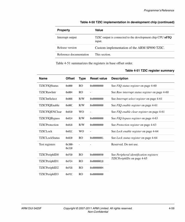
Programmer’s Reference
Table 4-51 summarizes the registers in base offset order.
Interrupt output TZIC output is connected to the development chip CPU nFIQ input.
Release version Custom implementation of the ARM SP890 TZIC.
Reference documentation This section.
Table 4-50 TZIC implementation in development chip (continued)
Property Value
Table 4-51 TZIC register summary
Name Offset Type Reset value Description
TZICFIQStatus 0x000 RO 0x00000000 See FIQ status register on page 4-60
TZICRawIntr 0x004 RO - See Raw interrupt status register on page 4-60
TZICIntSelect 0x008 R/W 0x00000000 See Interrupt select register on page 4-61
TZICFIQEnable 0x00C R/W 0x00000000 See FIQ enable register on page 4-61
TZICFIQENClear 0x010 WO - See FIQ enable clear register on page 4-61
TZICFIQBypass 0x014 R/W 0x00000000 See FIQ bypass register on page 4-63
TZICProtection 0x018 R/W 0x00000000 See Protection register on page 4-63
TZICLock 0x01C WO - See Lock enable register on page 4-64
TZICLockStatus 0x020 RO 0x00000001 See Lock status register on page 4-64
Test registers 0x300-0x310
- - Reserved. Do not use.
TZICPeriphID0 0xFE0 RO 0x00000090 See Peripheral identification registers TZICPeriphlDx on page 4-65
TZICPeriphID1 0xFE4 RO 0x00000018
TZICPeriphID2 0xFE8 RO 0x00000004
TZICPeriphID3 0xFEC RO 0x00000000
ARM DUI 0425F Copyright © 2007-2011 ARM Limited. All rights reserved. 4-59Non-Confidential

Programmer’s Reference
FIQ status register
The read-only TZICFIQStatus Register has a reset value of 0x00000000. It provides the status of the interrupts after FIQ masking. Table 4-52 lists the register bit assignments.
Raw interrupt status register
The read-only TZICRawIntr Register provides the status of the source interrupts, and software interrupts, to the interrupt controller. Table 4-53 lists the register bit assignments.
TZICPCellID0 0xFF0 RO 0x0000000D See TZICPCellID0 Register on page 4-68
TZICPCellID1 0xFF4 RO 0x000000F0
TZICPCellID2 0xFF8 RO 0x00000005
TZICPCellID3 0xFFC RO 0x000000B1
Table 4-51 TZIC register summary (continued)
Name Offset Type Reset value Description
Table 4-52 TZICFIQStatus Register bit assignments
Bits Name Function
[31:0] FIQStatus Shows the status of the interrupts after masking by the TZICFIQIntEnable and TZICFIQIntEnClear Registers.
A HIGH bit indicates that the interrupt is active, and generates an nFIQ interrupt to the processor.
Table 4-53 TZICRawIntr Register bit assignments
Bits Name Function
[31:0] RawIntr Shows the status of the interrupts before masking by the TZICFIQIntEnable and TZICFIQIntEnClear Registers.
A HIGH bit indicates that the interrupt is active before masking.
4-60 Copyright © 2007-2011 ARM Limited. All rights reserved. ARM DUI 0425FNon-Confidential

Programmer’s Reference
Interrupt select register
The read-write TZICIntSelect Register has a reset value of 0x00000000. It selects whether you can use the corresponding input source to generate a FIQ interrupt or whether it passes through to TZICIRQOUT. Table 4-54 lists the register bit assignments.
FIQ enable register
The read/write TZICFIQEnable Register has a reset value of 0x00000000. It enables the corresponding FIQ-selected input source. This interrupt source can then generate an FIQ interrupt. Table 4-55 lists the register bit assignments.
FIQ enable clear register
The write-only TZICFIQEnClear Register clears bits in the TZICFIQEnable Register. See FIQ enable register. Table 4-56 on page 4-62 lists the register bit assignments.
Table 4-54 TZICIntSelect Register bit assignments
Bits Name Function
[31:0] IntSelect Selects whether the interrupt source generates an FIQ interrupt or passes straight through to TZICIRQOUT.
0 = interrupt passes through to TZICIRQOUT1 = interrupt is available for FIQ generation.
Table 4-55 TZICFIQEnable Register bit assignments
Bits Name Function
[31:0] FIQEnable Enables the FIQ-selected interrupt lines, allowing the interrupts to reach the processor. Read:
0 = interrupt disabled
1 = interrupt enabled.
You can only enable the interrupt using this register. You must use the TZICFIQEnClear Register to disable the interrupt enable.
Write:
0 = no effect
1 = interrupt enabled.
Resetting disables all interrupts. There is 1 bit of the register for each interrupt source.
ARM DUI 0425F Copyright © 2007-2011 ARM Limited. All rights reserved. 4-61Non-Confidential

Programmer’s Reference
Table 4-56 TZICFIQEnClear Register bit assignments
Bits Name Function
[31:0] FIQEnClear Clears bits in the TZICFIQEnable Register.
Writing a HIGH clears the corresponding bit in the TZICFIQEnable Register.
Writing a LOW has no effect.
4-62 Copyright © 2007-2011 ARM Limited. All rights reserved. ARM DUI 0425FNon-Confidential

Programmer’s Reference
FIQ bypass register
The read/write TZICFIQBypass Register has a reset value of 0x00000000. It enables nNSFIQIN to be routed directly to nFIQ. By doing this, it bypasses all internal TZIC logic.
Figure 4-14 shows the register bit assignments.
Figure 4-14 TZICFIQBypass Register bit assignments
Table 4-57 lists the register bit assignments.
Protection register
The read/write TZICProtection Register has a reset value of 0x00000000. It enables or disables protected register access, stopping register accesses when the processor is in user-mode.
Figure 4-15 shows the register bit assignments.
Figure 4-15 TZICProtection Register bit assignments
31 1 0
Undefined
FIQBypass
Table 4-57 TZICFIQBypass Register bit assignments
Bits Name Function
[31:1] - Read undefined. Write as zero.
[0] FIQBypass Enables nNSFIQIN to route directly to nFIQ.
0=No Bypass
1=Bypass.
31 1 0
Undefined
Protection
ARM DUI 0425F Copyright © 2007-2011 ARM Limited. All rights reserved. 4-63Non-Confidential

Programmer’s Reference
Table 4-58 lists the register bit assignments.
Lock enable register
The write-only TZICLock Register enables or disables all other register write access. You must write the access code to this register before you can modify any other register. To disable access, you must write any other value to the register. The register protects the TZIC from spurious writes. The Lock bit in the TZICLockStatus Register indicates the status of the lock. See FIQ status register on page 4-60. Table 4-59 lists the register bit assignments.
Lock status register
The read-only TZICLockStatus Register provides the lock status of the TZIC registers.
Figure 4-16 shows the register bit assignments.
Figure 4-16 TZICLockStatus Register bit assignments
Table 4-58 TZICProtection Register bit assignments
Bits Name Function
[31:1] - Read undefined. Write as zero.
[0] Protection Enables or disables protected register access:
0 = protection mode disabled
1 = protection mode enabled.
When enabled, you can only make privileged mode accesses (reads and writes) to the TZIC. You can only access this register in privileged mode, even when protection mode is disabled.
Table 4-59 TZICLock Register bit assignments
Bits Name Function
[31:0] Lock To enable access to the other registers in the TZIC, you must write the correct access code of 0x0ACCE550 to this register. To disable access to the other TZIC registers, you must write any other value than 0x0ACCE550 to this register.
31 1 0
Undefined
Locked
4-64 Copyright © 2007-2011 ARM Limited. All rights reserved. ARM DUI 0425FNon-Confidential

Programmer’s Reference
Table 4-60 lists the register bit assignments.
Peripheral identification registers TZICPeriphlDx
The read-only TZICPeriphlD0-3 Registers are four 8-bit registers that span address locations 0xFE0 to 0xFEC. You can treat the registers conceptually as a single 32-bit register.
Figure 4-17 shows the register bit assignments of the TZICPeriphlD0-3 registers.
Figure 4-17 TZICPeriphlD0-3 registers bit assignments
Table 4-61 lists the peripheral identification registers bit assignments.
Table 4-60 TZICLockStatus Register bit assignments
Bits Name Function
[31:1] - Read undefined.
[0] Locked Shows the locked status of the TZIC:
0 = Access to the TZIC is not locked
1 = Access to the TZIC is locked (reset).
You can unlock the access using the TZICLock Register.
Part number
Part number 1
Part number 0
Designer0
Designer
Revision numberConfiguration
Configuration Revision number
Conceptual register bit assignment
Actual register bit assignment
7 0 7 4 3 0 7 4 3 0 7 0
Designer1
31 24 23 20 19 16 15 12 11 8 7 0
Table 4-61 TZICPeriphlD0-3 Register bit assignments
Bits Name Function
[31:24] Configuration Configuration option of the peripheral. The configuration value is 0.
[23:20] Revision number Revision number of the peripheral. The revision number starts from 0, and the value is revision independent.
[19:12] Designer Identification of the designer. ARM Limited is 0x41 (ASCII A).
[11:0] Part number Identification of the peripheral. Use the three-digit product code 0x890 for TZIC.
ARM DUI 0425F Copyright © 2007-2011 ARM Limited. All rights reserved. 4-65Non-Confidential

Programmer’s Reference
The read-only TZICPeriphID0 Register is hard-coded and the register fields register determine the reset value.
Figure 4-18 shows the register bit assignments.
Figure 4-18 TZICPeriphlDO Register bit assignments
Table 4-62 lists the register bit assignments.
See also:
• TZICPeriphlD1 Register
• TZICPeriphlD2 Register on page 4-67
• TZICPeriphlD3 Register on page 4-67.
TZICPeriphlD1 Register
The read-only TZICPeriphID1 Register is hard-coded and the fields within the register determine the reset value.
Figure 4-19 shows the register bit assignments.
Figure 4-19 TZICPeriphlD1 Register bit assignments
31 8 7 0
Undefined Partnumber0
7
Table 4-62 TZICPeriphID0 Register bit assignments
Bits Name Function
[31:8] - Read undefined
[7:0] Partnumber0 These bits read back as 0x90
31 8 7 4 3 0
Undefined Designer0
Partnumber1
4-66 Copyright © 2007-2011 ARM Limited. All rights reserved. ARM DUI 0425FNon-Confidential

Programmer’s Reference
Table 4-63 lists the register bit assignments.
TZICPeriphlD2 Register
The read-only TZICPeriphID2 Register is hard-coded and the fields within the register determine the reset value.
Figure 4-20 shows the register bit assignments.
Figure 4-20 TZICPeriphlD2 Register bit assignments
Table 4-64 lists the register bit assignments.
TZICPeriphlD3 Register
The read-only TZICPeriphID3 Register is hard-coded and the fields within the register determine the reset value.
Figure 4-21 on page 4-68 shows the register bit assignments.
Table 4-63 TZICPeriphID1 Register bit assignments
Bits Name Function
[31:8] - Read undefined
[7:4] Designer0 These bits read back as 0x1
[3:0] Partnumber1 These bits read back as 0x8
31 8 7 4 3 0
Undefined Revision Designer1
Table 4-64 TZICPeriphID2 Register bit assignments
Bits Name Function
[31:8] - Read undefined
[7:4] Revision These bits read back as the revision number and can be between 0 and 15
[3:0] Designer1 These bits read back as 0x4
ARM DUI 0425F Copyright © 2007-2011 ARM Limited. All rights reserved. 4-67Non-Confidential

Programmer’s Reference
Figure 4-21 TZICPeriphlD3 Register bit assignments
Table 4-65 lists the register bit assignments.
TZICPCellID0 Register
The read-only TZICPCelllD0-3 registers are four 8-bit registers that span address locations 0xFF0 to 0xFFC. You can treat the registers conceptually as a single 32-bit register. This register acts as a standard cross-peripheral identification system. Figure 4-22 shows the register bit assignments.
Figure 4-22 TZICPCelllD0-3 Registers bit assignments
The read-only TZICPCellID0 Register is hard-coded and the fields within the register determine the reset value. Table 4-66 lists the register bit assignments.
31 8 7 0
Undefined Configuration
Table 4-65 TZICPeriphID3 Register bit assignments
Bits Name Function
[31:8] - Read undefined
[7:0] Configuration These bits read back as 0x00
TZICPCellID3
Conceptual register bit assignment
Actual register bit assignment7 0 7 0 7 0 7 0
31 24 23 16 15 8
TZICPCellID2 TZICPCellID1 TZICPCellID0
TZICPCellID0TZICPCellID1TZICPCellID2TZICPCellID3
7 0
Table 4-66 TZICPCellID0 Register bit assignments
Bits Name Function
[31:8] - Read undefined
[7:0] TZICPCellID0 These bits read back as 0x0D
4-68 Copyright © 2007-2011 ARM Limited. All rights reserved. ARM DUI 0425FNon-Confidential

Programmer’s Reference
See also:
• TZICPCellID1 Register
• TZICPCellID2 Register
• TZICPCellID3 Register.
TZICPCellID1 Register
The read-only TZICPCellID1 Register is hard-coded and the fields within the register determine the reset value. Table 4-67 lists the register bit assignments.
TZICPCellID2 Register
The read-only TZICPCellID2 Register is hard-coded and the fields within the register determine the reset value. Table 4-68 lists the register bit assignments.
TZICPCellID3 Register
The read-only TZICPCellID3 Register is hard-coded and the fields within the register determine the reset value. Table 4-69 lists the register bit assignments.
Table 4-67 TZICPCellID1 Register bit assignments
Bits Name Function
[31:8] - Read undefined
[7:0] TZICPCellID1 These bits read back as 0xF0
Table 4-68 TZICPCellID2 Register bit assignments
Bits Name Function
[31:8] - Read undefined
[7:0] TZICPCellID2 These bits read back as 0x05
Table 4-69 TZICPCellID3 Register bit assignments
Bits Name Function
[31:8] - Read undefined
[7:0] TZICPCellID3 These bits read back as 0xB1
ARM DUI 0425F Copyright © 2007-2011 ARM Limited. All rights reserved. 4-69Non-Confidential

Programmer’s Reference
4.11.2 Development chip GIC
There is one GIC in the development chip. Table 4-70 lists the details for the GIC in the development chip.
4.11.3 Development chip interrupt signals
In the development chip, Secure interrupt sources can be routed to the nFIQ input on the core, and non-secure sources can be routed to the nIRQ input on the core. To enable the routing, a TZIC is implemented to control routing to the TZIC or non-secure-IC logic as appropriate for the application.
All interrupt sources, on-chip and off-chip, are routed to the TZIC, enabling an entirely dynamic interrupt configuration to be defined as part of the secure boot process. It is the responsibility of the end user to ensure that a secure interrupt is generated only by a securely decoded peripheral in a secure system design.
By default, the majority of PB1176JZF-S interrupts trigger nIRQ events through the GIC chain. However, in a TrustZone aware system implementation, the nFIQ can be considered a security interrupt, and consequently very flexible interrupt handling is available.
Table 4-70 GIC implementation in development chip
Property Value
Location ARM1176JZF-S development chip
Memory base addresses 0x10120000 (GIC CPU interface)
0x10121000 (GIC distribution interface)
Interrupt inputs See Table 4-71 on page 4-72.
Interrupt output Development chip GIC nIRQ output is connected to the development chip CPU nIRQ input
Note The development chip TZIC nFIQ output is connected to the development chip CPU nFIQ input.
Release version Pre-release implementation of the ARM PL390 GIC.
Reference documentation For more information on the GIC registers, see GIC Distribution register on page 4-77, GIC CPU Interface on page 4-100, and GIC reserved register addresses on page 4-105.
4-70 Copyright © 2007-2011 ARM Limited. All rights reserved. ARM DUI 0425FNon-Confidential

Programmer’s Reference
The TZIC on the ARM1176JZF-S development chip is capable of overriding designated interrupt source(s) from reaching the GIC, and generating an nFIQ instead of the nIRQ for the overridden interrupt source.
When an interrupt, either nIRQ or nFIQ, occurs in a TrustZone aware software system, it is handled in one of three vector tables:
• one is associated with the Normal World exception vector usage
• one is associated with the Secure World exception vector usage
• one is associated with the Secure World Monitor Mode exception vector usage.
To a non-TrustZone aware software system, this handling defaults to the previous ARM exception handling setup and capabilities.
A CP15 security control register can designate whether a given nFIQ or nIRQ is handled in the current operating world, or causes the exception to be handled by the Monitor Mode exception table. This enables Monitor Mode code to control routing of nFIQ and nIRQ to the correct operating World, either Secure or Normal.
Normally you use nFIQ as the Secure interrupt, because it is possible for the Secure World to block masking of the nFIQ by the Normal World. The Secure World cannot do the same for the nIRQ.
Note This routing is under software control, a system might choose to deploy the nFIQ for its own purposes, rather than as a secure world interrupt.
Examples of interrupt handling are:
An interrupt occurs while the core is in the correct world.
• nIRQ or nFIQ occurs while core is running in World A
• nIRQ or nFIQ is designated for handling by World A
• Exception vectors through that World A exception table
• World A ISR handles interrupt.
An interrupt occurs while the core is in the wrong world.
• nIRQ or nFIQ occurs while core is running in World A
• nIRQ or nFIQ is designated for handling by World B
• Exception uses the Monitor mode exception table
• Monitor Mode code transfers state information so core can start safely in world B
• Monitor code returns to execution in World B
• Exception vectors through that World B exception table
• World B ISR handles interrupt.
ARM DUI 0425F Copyright © 2007-2011 ARM Limited. All rights reserved. 4-71Non-Confidential
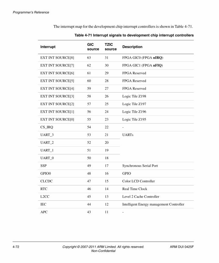
Programmer’s Reference
The interrupt map for the development chip interrupt controllers is shown in Table 4-71.
Table 4-71 Interrupt signals to development chip interrupt controllers
InterruptGIC source
TZIC source
Description
EXT INT SOURCE[8] 63 31 FPGA GIC0 (FPGA nIRQ)
EXT INT SOURCE[7] 62 30 FPGA GIC1 (FPGA nFIQ)
EXT INT SOURCE[6] 61 29 FPGA Reserved
EXT INT SOURCE[5] 60 28 FPGA Reserved
EXT INT SOURCE[4] 59 27 FPGA Reserved
EXT INT SOURCE[3] 58 26 Logic Tile Z198
EXT INT SOURCE[2] 57 25 Logic Tile Z197
EXT INT SOURCE[1] 56 24 Logic Tile Z196
EXT INT SOURCE[0] 55 23 Logic Tile Z195
CS_IRQ 54 22 -
UART_3 53 21 UARTs
UART_2 52 20
UART_1 51 19
UART_0 50 18
SSP 49 17 Synchronous Serial Port
GPIO0 48 16 GPIO
CLCDC 47 15 Color LCD Controller
RTC 46 14 Real Time Clock
L2CC 45 13 Level 2 Cache Controller
IEC 44 12 Intelligent Energy management Controller
APC 43 11 -
4-72 Copyright © 2007-2011 ARM Limited. All rights reserved. ARM DUI 0425FNon-Confidential
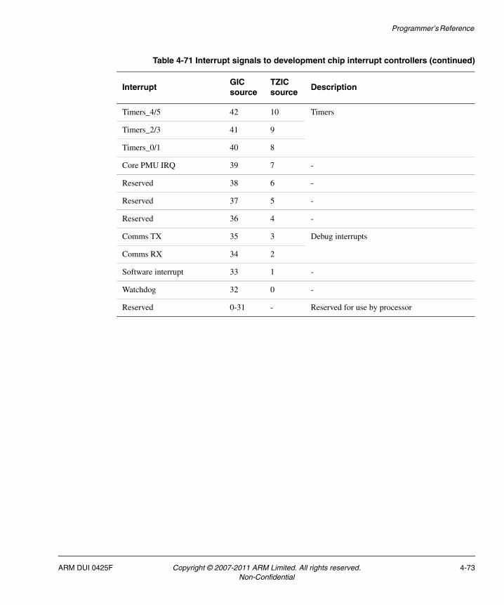
Programmer’s Reference
Timers_4/5 42 10 Timers
Timers_2/3 41 9
Timers_0/1 40 8
Core PMU IRQ 39 7 -
Reserved 38 6 -
Reserved 37 5 -
Reserved 36 4 -
Comms TX 35 3 Debug interrupts
Comms RX 34 2
Software interrupt 33 1 -
Watchdog 32 0 -
Reserved 0-31 - Reserved for use by processor
Table 4-71 Interrupt signals to development chip interrupt controllers (continued)
InterruptGIC source
TZIC source
Description
ARM DUI 0425F Copyright © 2007-2011 ARM Limited. All rights reserved. 4-73Non-Confidential

Programmer’s Reference
4.12 Interrupt controllers in the FPGA
There are two GICs in the FPGA. Table 4-72 lists the details of the GICs in the FPGA.
See the following sections for more information on the interrupt signals and the GIC controllers:
• FPGA interrupt signals
• GIC Distribution register on page 4-77
• GIC CPU Interface on page 4-100
• GIC reserved register addresses on page 4-105.
Table 4-72 GIC implementation in FPGA
Property Value
Location FPGA
Memory base addresses GIC0 CPU interface 0x10040000
GIC0 Distributor 0x10041000
GIC1 CPU interface 0x10050000
GIC1 Distributor 0x10051000
Interrupt inputs See Table 4-73 on page 4-75.
Interrupt output GIC0 nIRQ to input 31 and GIC1 nFIQ to input 30 of the TZIC on the development chip
Release version Pre-release implementation of the ARM PL390 GIC
Reference documentation See FPGA interrupt signals and Development chip interrupt signals on page 4-70
The GICs in the FPGA are the same as the GICs in the development chip except that the development chip GIC has 64 interrupt sources and the FPGA GICs have 32 interrupt sources. A summary of the registers in the FPGA GICs is provided in Table 4-74 on page 4-77.
For more information on the GIC registers, see GIC Distribution register on page 4-77, GIC CPU Interface on page 4-100, and GIC reserved register addresses on page 4-105.
4-74 Copyright © 2007-2011 ARM Limited. All rights reserved. ARM DUI 0425FNon-Confidential

Programmer’s Reference
4.12.1 FPGA interrupt signals
The bit assignments for the two GIC interrupt controllers in the FPGA are listed in Table 4-73 on page 4-75. Each bit corresponds to an interrupt source. Use the bit to enable or disable the interrupt or to check the interrupt status.
Note The primary and secondary interrupt controllers in the FPGA (GIC0 and GIC1) share interrupt inputs, but the interrupt outputs are routed differently:
• GIC0 generates an nIRQ which corresponds to development chip EXT INT SOURCE[8] and TZIC Source 31.
• GIC1 generates an nFIQ which corresponds to development chip EXT INT SOURCE[7] and TZIC Source 30.
Table 4-73 Interrupt signals to FPGA primary and secondary GICs
Interrupt Interrupt source Description
63 Reserved Logic Tile
62 Reserved Logic Tile
61 Reserved FPGA
60 Reserved FPGA
59 Reserved FPGA
58 Reserved FPGA
57 RTC Real Time Clock
56 Reserved FPGA
55 Reserved FPGA
54 Reserved FPGA
53 Reserved FPGA
52 DoC IRQ (Reserved) FPGA
51 AACI Audio CODEC controller
50 Reserved FPGA
49 Reserved FPGA
ARM DUI 0425F Copyright © 2007-2011 ARM Limited. All rights reserved. 4-75Non-Confidential

Programmer’s Reference
48 PISMO Reserved for memory expansion. (Not driven by standard static memory expansion board.)
47 PCI3 Interrupt 3 triggered from external PCI bus
46 PCI2 Interrupt 2 triggered from external PCI bus
45 PCI1 Interrupt 1 triggered from external PCI bus
44 PCI0 Interrupt 0 triggered from external PCI bus
43 USB USB controller
42 ETHERNET Ethernet controller
41 GPIO2 GPIO controller
40 GPIO1 GPIO controller
39 Character LCD Character LCD
38 UART4 UART in FPGA
37 SCI Smart Card Interface
36 KMI1 Activity on mouse port
35 KMI0 Activity on keyboard port
34 Reserved Unused. This was MCI[1] on the Emulation Baseboard
33 MCI Multimedia Card Interface
32 Reserved FPGA
Table 4-73 Interrupt signals to FPGA primary and secondary GICs (continued)
Interrupt Interrupt source Description
4-76 Copyright © 2007-2011 ARM Limited. All rights reserved. ARM DUI 0425FNon-Confidential

Programmer’s Reference
4.12.2 GIC Distribution register
This section describes the GIC Distributor registers:
• Summary of GIC Distribution registers
• Distributor Register Control Register on page 4-78
• Interrupt Controller Type Register on page 4-79
• Interrupt Set-Enable Registers on page 4-80
• Interrupt Clear-Enable Registers on page 4-81
• Interrupt Set-Pending Registers on page 4-83
• Interrupt Clear-Pending Registers on page 4-84
• Active Bit Registers on page 4-86
• Interrupt Priority Registers on page 4-86
• Interrupt CPU Target Registers on page 4-90
• Interrupt Configuration Registers on page 4-93
• Software Interrupt Register on page 4-99.
See Interrupt controllers on page 3-19 for a description of interrupt signal routing.
Note The GIC in the development chip has 64 interrupt source inputs, but interrupts 0–31 are reserved for use by the processor.
The GICs in the FPGA each have only 32 interrupt source inputs (32–64). Interrupt inputs 0–31 are not used. The interrupt inputs are shared by both FPGA GICs.
Summary of GIC Distribution registers
Table 4-74 lists the Distribution registers in the FPGA GICs.
Table 4-74 FPGA Register summary
Register name Base offset Type Width Reset Description
IrqControllerType 0x004 Read/Write 8 00000001 Interrupt controller type register
IrqEnSet0 0x100 Read/Write 32 0000FFFF Irq 0 to 31 set-enable register (reserved)
IrqEnSet1 0x104 Read/Write 32 00000000 Irq 32 to 63 set-enable register
IrqEnClr0 0x180 Read/Write 32 0000FFFF Irq 0 to 31 clear-enable register (reserved)
IrqEnClr1 0x184 Read/Write 32 00000000 Irq 32 to 63 clear-enable register
IrqPenSet0 0x200 Read/Write 32 00000000 Irq 0 to 31 set-pending register (reserved)
ARM DUI 0425F Copyright © 2007-2011 ARM Limited. All rights reserved. 4-77Non-Confidential

Programmer’s Reference
Distributor Register Control Register
Figure 4-23 shows the bit assignments for this register.
Figure 4-23 Distributor Register Control Register bit assignments
IrqPenSet1 0x204 Read/Write 32 00000000 Irq 32 to 63 set-pending register
IrqPenClr0 0x280 Read/Write 32 00000000 Irq 0 to 31 clear-pending register (reserved)
IrqPenClr1 0x284 Read/Write 32 00000000 Irq 32 to 63 clear-pending register
IrqActiveBit0 0x300 Read Only 32 00000000 Irq 0 to 31 active bit register (reserved)
IrqActiveBit1 0x304 Read Only 32 00000000 Irq 32 to 63 active bit register
IrqPriority0 0x400 Read/Write 16 00000000 Irq 0 to 3 priority register (reserved)
IrqPriority1 0x404 Read/Write 16 00000000 Irq 4 to 7 priority register (reserved)
IrqPriority2 0x408 Read/Write 16 00000000 Irq 8 to 11 priority register (reserved)
IrqPriority3 0x40C Read/Write 16 00000000 Irq 12 to 15 priority register (reserved)
IrqPriority4 0x410 Read Only 16 00000000 Irq 16 to 19 priority register (reserved)
IrqPriority5 0x414 Read Only 16 00000000 Irq 20 to 23 priority register (reserved)
IrqPriority6 0x418 Read Only 16 00000000 Irq 24 to 27 priority register (reserved)
IrqPriority7 0x41C Read Only 16 00000000 Irq 28 to 31 priority register (reserved)
IrqPriority8 0x420 Read/Write 16 00000000 Irq 32 to 35 priority register
IrqPriority9 0x424 Read/Write 16 00000000 Irq 36 to 39 priority register
IrqPriority10 0x428 Read/Write 16 00000000 Irq 40 to 43 priority register
IrqPriority11 0x42C Read/Write 16 00000000 Irq 44 to 47 priority register
Table 4-74 FPGA Register summary (continued)
Register name Base offset Type Width Reset Description
31 8 0
Undefined
1
Enable
4-78 Copyright © 2007-2011 ARM Limited. All rights reserved. ARM DUI 0425FNon-Confidential

Programmer’s Reference
Table 4-75 lists the bit assignments for the register at offset 0x000.
Interrupt Controller Type Register
Figure 4-24 shows the bit assignments for this register.
Figure 4-24 Interrupt Controller Type Register bit assignments
Table 4-76 lists the bit assignments for the register at offset 0x004.
You can use the number of IT lines to determine which sets of registers in the Distributor register map are populated. In the ARM1176JZF core, IT lines is hard-coded to 5'b00001, indicating 64 interrupt sources.
The CPU number is encoded as:
000 System contains 1 CPU.
Table 4-75 Distributor Register Control Register bit assignments
Bits Name Type Function
[31:1] - Read/Write Undefined, SBZ.
[0] Enable Read/Write Distributor enable. If this bit is 0, no interrupts are sent out of the distributor. Disabling the distributor while there are pending interrupts might give rise to spurious interrupts as a result of the inherent timing race between the disabling of the interrupt and the CPU response to pending interrupts.
Undefined
31 8 5 4 0
CPU numberIT lines number
7
Table 4-76 Interrupt Controller Type Register bit assignments
Bits Name Type Function
[31:8] Read/Write Undefined, SBZ
[7:5] CPU number Read/Write CPU number encoding for the ARM1176 development chip is:000: System contains 1 CPU.
[4:0] IT lines number Read/Write IT lines number encoding for the GIC in the ARM1176 development chip is as follows:00001: 64 interrupts support, 32 interrupt lines support.
ARM DUI 0425F Copyright © 2007-2011 ARM Limited. All rights reserved. 4-79Non-Confidential

Programmer’s Reference
001 System contains 2 CPUs.
010 System contains 3 CPUs.
011 System contains 4 CPUs.
0xx Reserved for future extension.
Note The CPU number indicates the number of CPUs in the system. The CPU number for the ARM 1176JZF development chip is always 1.
Interrupt Set-Enable Registers
These registers control an enable bit for each interrupt in the interrupt distributor.
The GIC in the development chip supports 64 interrupts:
• 32 software interrupts
• 32 hardware interrupts.
Figure 4-25 shows the bit assignments for Interrupt Set-Enable Register 0.
Figure 4-25 Interrupt Set-Enable Register 0 bit assignments
Table 4-77 lists the bit assignments for Interrupt Set-Enable Register 0 at offset 0x100.
31 29 28 16 15 0
Interrupt enable (RO) Interrupt enable (RO)
Interrupt enable (RW)
Table 4-77 Interrupt Set-Enable Register 0 bit assignments
Bits Name Type Function
[31:29] Interrupt enable Read/Write Bit 31 is for the legacy nIRQ pin. Bit 30 is for a private watchdog in an MPCore system and is not used in this SoC. Bit 29 is for a private timer in an MPCore system and is not used in this SoC.
[28:16] Interrupt enable Read Only Undefined interrupts, read as 0.
[15:0] Interrupt enable Read Only Interrupts 0 to 15 are inter-processor, or reserved for software use. Read as 1.
4-80 Copyright © 2007-2011 ARM Limited. All rights reserved. ARM DUI 0425FNon-Confidential

Programmer’s Reference
Figure 4-26 shows the bit assignments for Interrupt Set-Enable Register 1.
Figure 4-26 Interrupt Set-Enable Register 1 bit assignments
Table 4-78 lists the bit assignments for Interrupt Set-Enable Register 1 at offset 0x104.
In these registers, writing a 1 sets the corresponding interrupt enable bit, and a read reads back a 1. When this is set, you can only clear it by using the Enable-Clear Register. In other words, writing a 0 to the Set-Enable Register does not write a 0 to the corresponding interrupt enable bit.
The values read in the Set-Enable Registers, for a particular range of interrupts, represent currently enabled interrupts. Non-present interrupts, depending on the Interrupt Number field of the Interrupt Controller Type Register related fields are read as zero, and writing to these fields has no effect.
Interrupt Clear-Enable Registers
These registers control an enable bit for each interrupt in the interrupt distributor. There can be up to eight Clear-Enable registers. Because the GIC in the ARM1176JZF Development Chip only supports 64 interrupts, it has two such registers and the rest are unused.
Figure 4-27 shows the bit assignments for this register.
Figure 4-27 Interrupt Clear-Enable Register 0 bit assignments
31 0
Interrupt enable (RW)
Table 4-78 Interrupt Set-Enable Register 1 bit assignments
Bits Name Type Function
[31:0] Interrupt enable Read/Write Writing a 1 sets the interrupt enable bit and so, the interrupt is transmitted to the targeted CPU.
31 29 28 16 15 0
Interrupt enable (RO) Interrupt enable (RO)
Interrupt enable (RW)
ARM DUI 0425F Copyright © 2007-2011 ARM Limited. All rights reserved. 4-81Non-Confidential

Programmer’s Reference
Table 4-79 lists the bit assignments for the register at offset 0x180.
Figure 4-28 shows the bit assignments for Interrupt Clear-Enable Register 1.
Figure 4-28 Interrupt Clear-Enable Register 1 bit assignments
Table 4-80 lists the bit assignments for the Interrupt Clear-Enable Register 1 at offset 0x184.
Writing a 1 clears the corresponding interrupt enable bit and a read reads back a 0. When cleared, you can only set this bit by using the Set-Enable Register. In other words, writing a 1 to the Clear-Enable Register does not write a 1 to the corresponding interrupt enable bit.
The values read in the Clear-Enable Registers, for a particular range of interrupts, represent currently enabled interrupts. Non-present interrupts, depending on the Interrupt number field of the Interrupt Controller Type Register, related fields are read as zero and writing to these fields has no effect.
Table 4-79 Interrupt Clear-Enable Register 0 bit assignments
Bits Name Type Function
[31:29] Interrupt enable Read/Write Writing a 1 clears the interrupt enable bit and it reads a 0.
Bit 31 is for the legacy nIRQ pin.
Bit 30 is for a private watchdog in an MPCore system and is not used in this SoC.
Bit 29 is for a private timer in an MPCore system and is not used in this SoC.
[28:16] Interrupt enable Read Only Undefined interrupts, read as 0.
[15:0] Interrupt enable Read Only Interrupts 0 to 15 are inter-processor or reserved for software use. Read as 0.
31 0
Interrupt enable (RW)
Table 4-80 Interrupt Clear-Enable Register 1 bit assignments
Bits Name Type Function
[31:0] Interrupt enable Read/Write Writing a 1 clears the interrupt enable bit and it reads a 0.
4-82 Copyright © 2007-2011 ARM Limited. All rights reserved. ARM DUI 0425FNon-Confidential

Programmer’s Reference
Interrupt Set-Pending Registers
These registers indicate the interrupts that are currently in pending state, bit read as 1, or to force some interrupts to enter pending state by overriding event detection on interrupt lines. Each set register is used for 32 interrupts therefore, the ARM1176 development chip uses two such registers.
Figure 4-41 on page 4-96 shows the bit assignments for Interrupt Set-Pending Register 0.
Figure 4-29 Interrupt Set-Pending Register 0 bit assignments
Table 4-81 lists the bit assignments for the Interrupt Set-Pending Register 0 at offset 0x200.
Figure 4-30 shows the bit assignments for Interrupt Set-Pending Register 1.
Figure 4-30 Interrupt Set-Pending Register 1 bit assignments
31 29 28 16 15 0
Interrupt pending (RO) Interrupt pending (RO)
Interrupt pending (RW)
Table 4-81 Interrupt Set-Pending Register 0 bit assignments
Bits Name Type Function
[31:29] Interrupt pending Read/Write Writing 1 sets the interrupt pending bit and the corresponding interrupt enters pending state.
Bit 31 is for the legacy nIRQ pin.
Bit 30 is for private watchdog in an MPCore system and is not used in this SoC.
Bit 29 is for private timer in an MPCore system and is not used in this SoC.
[28:16] Interrupt pending Read Only Undefined interrupts, read as 0.
[15:0] Interrupt pending Read Only Writing to IT0 to IT15 has not effect. Only the Software Interrupt Register can trigger these interrupts.
31 0
Interrupt pending (RW)
ARM DUI 0425F Copyright © 2007-2011 ARM Limited. All rights reserved. 4-83Non-Confidential

Programmer’s Reference
Table 4-82 lists the bit assignments for Interrupt Set-Pending Register 1 at offset 0x204.
Note • You can only perform reads and writes by enabling the distributor through the
distributor control register. described in Distributor Register Control Register on page 4-78.
• For read status, you must set interrupt targets in the CPU targets registers, corresponding to hardware IRQs 32-63.
Writing a 1 to a bit through the Set-Pending Register means that the corresponding interrupt enters pending state. Writing a 1 sets the corresponding interrupt pending bit and a read reads back a 1. When set, you can only clear this bit using the Clear-Pending Register. Writing a 0 to the Set-Pending Register does not write a 0 to the corresponding interrupt pending bit.
Note All RESERVED interrupts, spurious interrupts, and non-present interrupts, depending on the Interrupt Number field of the Interrupt Controller Type Register, and related fields are read as zero and writing to these fields has no effect.
The values read in the Set-Pending and Clear-Pending registers for the same interrupts range are the same. They both represent current pending interrupts. If a bit is read as 1, it implies that the interrupt is pending for at least one CPU.
Interrupt Clear-Pending Registers
These registers either determine that the registers that are currently in pending state and the bit is read as 1, or they force pending interrupts to return to the inactive state. Each set register is used for 32 interrupts. The ARM1176 Development Chip uses two such registers. The remaining ones are unused.
Figure 4-31 on page 4-85 shows the bit assignments for Interrupt Clear-Pending Register 0.
Table 4-82 Interrupt Set-Pending Register 1 bit assignments
Bits Name Type Function
[31:0] Interrupt pending Read/Write Writing 1 sets the interrupt pending bit and the corresponding interrupt enters pending state
4-84 Copyright © 2007-2011 ARM Limited. All rights reserved. ARM DUI 0425FNon-Confidential

Programmer’s Reference
Figure 4-31 Interrupt Clear-Pending Register 0 bit assignments
Table 4-83 lists the bit assignments for Interrupt Clear-Pending Register 0 at offset 0x280.
Figure 4-32 shows the bit assignments for Interrupt Clear-Pending Register 1.
Figure 4-32 Interrupt Clear-Pending Register 1 bit assignments
Table 4-84 lists the bit assignments for Interrupt Clear-Pending Register 1 at offset 0x284.
31 29 28 16 15 0
Interrupt pending (RO) Interrupt pending (RO)
Interrupt pending (RW)
Table 4-83 Interrupt Clear-Pending Register 0 bit assignments
Bits Name Type Function
[31:29] Interrupt pending Read/Write Writing a 1 clears the interrupt enable bit and the corresponding interrupt enters pending state. A read returns a 0.
Bit 31 is for the legacy nIRQ pin.
Bit 30 is for private watchdog in an MPCore system and is not used in this SoC.
Bit 29 is for private timer in an MPCore system and is not used in this SoC.
[28:16] Interrupt pending Read Only Undefined interrupts, read as 0.
[15:0] Interrupt pending Read Only Writing to bits corresponding to IT0 to IT15 has no effect. Only the Software Interrupt Register can trigger these interrupts.
31 0
Interrupt pending
Table 4-84 Interrupt Clear-Pending Register 1 bit assignments
Bits Name Type Function
[31:0] Interrupt pending Read/Write Writing a 1 clears the interrupt enable bit and the corresponding interrupt enters pending state. A read returns a 0.
ARM DUI 0425F Copyright © 2007-2011 ARM Limited. All rights reserved. 4-85Non-Confidential

Programmer’s Reference
Writing a 1 clears the corresponding interrupt pending bit and a read reads back a 0. When cleared, you can only set this bit by using the Enable-Set Register. In other words, writing a 1 to the Enable-Clear Register does not write a 1 to the corresponding interrupt enable bit.
Note All RESERVED interrupts, spurious interrupts, and non-present interrupts, depending on the Interrupt number field of the Interrupt Controller Type Register, and related fields are read as zero and writing to these fields has no effect.
The values read in the Pending-Set and Pending-Clear registers for the same interrupts range are the same, and represent current pending interrupts. If a bit is read as 1, it implies that the interrupt is pending.
Active Bit Registers
The Active Bit Register enables the software to find out the interrupts that are currently active, bit read as 1. They are read-only registers and writes to these registers are ignored. Because each register only handles 32 interrupts, there are two such registers in the chip.
Figure 4-33 Active Bit Register 0 and 1 bit assignments
Table 4-85 lists the bit assignments for the registers at offset 0x200–0x304.
Interrupt Priority Registers
These registers store the individual interrupt priority and16 levels of priority are supported.
31 0
Interrupt active bit
Table 4-85 Active Bit Register 0 and 1 bit assignments
Bits Name Type Function
[31:0] Interrupt active bit Read Only Bit reads as 1: Corresponding interrupt is active
Bit reads as 0: Corresponding interrupt is inactive
4-86 Copyright © 2007-2011 ARM Limited. All rights reserved. ARM DUI 0425FNon-Confidential

Programmer’s Reference
Because each register sets the priority of four interrupts, there are 16 such registers in the ARM1176 Development Chip. You can set the priority for each interrupt by writing a value between 0x0-0xF to the corresponding bits for the interrupts in the registers described in this section. An interrupt with priority 0x0 has the highest priority, and an interrupt with priority 0xF is the lowest priority.
Note You must never set the priority for an interrupt equal to the Priority Mask Register under normal operation. This is because the CPU interface does a strict comparison between the pending interrupt priority and the priority mask set in the Priority Mask Register. See GIC reserved register addresses on page 4-105. Because of this, if the priority mask is set to 0xF, interrupts of priority 0xF are not executed.
For interrupts with equal priority, the interrupt with the lowest ID is handled first, the interrupt with the second lowest ID is handled second, and the interrupt with the third lowest ID is handled third. If the two interrupts have the same ID, this can be the case for software interrupts, the lowest CPU source ID is executed first.
Figure 4-34 shows the bit assignments for Interrupt Priority Register 0-3.
Figure 4-34 Interrupt Priority Register 0-3 bit assignments
31 28 27 24 23 20 16 15 12 11 8 7 4 3 019
Priority N+3 Priority N+2 Priority N+1 Priority N SBZSBZSBZ SBZ
ARM DUI 0425F Copyright © 2007-2011 ARM Limited. All rights reserved. 4-87Non-Confidential

Programmer’s Reference
Table 4-86 lists the bit assignments for Interrupt Priority Register 0-3 at offset 0x400–0x40C.
Figure 4-35 shows the bit assignments for the Interrupt Priority Register 4-6 registers.
Figure 4-35 Interrupt Priority Register 4-6 bit assignments
Table 4-86 Interrupt Priority Register 0-3 bit assignments
Bits Name Type Function
[31:28] Priority N+3 Read/Write Interrupt priority
[27:24] SBZ
[23:20] Priority N+2
[19:16] SBZ
[15:12] Priority N+1
[11:8] SBZ
[7:4] Priority N
[3:0] SBZ
31 28 27 24 23 20 16 15 12 11 8 7 4 3 019
Priority N+3 Priority N+2 Priority N+1 Priority N SBZSBZSBZ SBZ
4-88 Copyright © 2007-2011 ARM Limited. All rights reserved. ARM DUI 0425FNon-Confidential

Programmer’s Reference
Table 4-87 lists the bit assignments for the Interrupt Priority Register 4-6 registers at offset 0x410–0x418.
Figure 4-36 shows the bit assignments for the Interrupt Priority Register 7-15 registers.
Figure 4-36 Interrupt Priority Register 7-15 bit assignments
Table 4-87 Interrupt Priority Register 4-6 bit assignments
Bits Name Type Function
[31:28] Priority N+3 Read Only Interrupt priority
[27:24] SBZ
[23:20] Priority N+2
[19:16] SBZ
[15:12] Priority N+1
[11:8] SBZ Read Only Interrupt priority
[7:4] Priority N
[3:0] SBZ
31 28 27 24 23 20 16 15 12 11 8 7 4 3 019
Priority N+3 Priority N+2 Priority N+1 Priority N SBZSBZSBZ SBZ
ARM DUI 0425F Copyright © 2007-2011 ARM Limited. All rights reserved. 4-89Non-Confidential

Programmer’s Reference
Table 4-88 lists the bit assignments for the Interrupt Priority Register 7-15 registers at offset 0x41C–0x43C.
Interrupt CPU Target Registers
These registers store the list of CPUs that each interrupt is sent to if the event defined by the Interrupt Controller Type Register occurs. Each bit in the Interrupt CPU Targets Register refers to one CPU. For the ARM1176JZF Development Chip, only one core is relevant. These registers are ignored in the case of software triggered interrupts.
This section describes the format of interrupt Interrupt CPU Targets Registers. Because each register is used for four interrupts, there are 16 registers in the development chip.
Figure 4-37 shows the bit assignments for the Interrupt CPU Target Registers 0-6 registers.
Figure 4-37 Interrupt CPU Target Registers 0-6 bit assignments
Table 4-88 Interrupt Priority 7-15 Register bit assignments
Bits Name Type Function
[31:28] Priority N+3 Read/Write Interrupt priority
[27:24] SBZ
[23:20] Priority N+2
[19:16] SBZ
[15:12] Priority N+1
[11:8] SBZ
[7:4] Priority N
[3:0] SBZ
31 24 23 16 15 8 7 0
CPU targets NCPU targets N+1CPU targets N+2CPU targets N+3
4-90 Copyright © 2007-2011 ARM Limited. All rights reserved. ARM DUI 0425FNon-Confidential

Programmer’s Reference
Table 4-89 lists the bit assignments for the Interrupt CPU Target Registers 0-6 registers at 0x800–0x818.
Figure 4-38 shows the bit assignments for the Interrupt CPU Target Register 7 at 0x81C.
Figure 4-38 Interrupt CPU Target Register 7 bit assignments
Table 4-90 lists the Interrupt CPU Target Register 7 bit assignments.
This register is for interrupts IT28, IT29, IT30, and IT31.
Table 4-89 Interrupt CPU Target Registers 0-6 bit assignments
Bits Name Type Function
[31:24] CPU targets N+3a
a. Only one cpu is active and it is always CPU0.
Read Only Store list of CPUs that are sent interrupts
[23:16] CPU targets N+2
[15:8] CPU targets N+1
[7:0] CPU targets N
31 24 23 16 15 8 7 0
CPU targets NCPU targets N+1CPU targets N+2CPU targets N+3
Table 4-90 Interrupt CPU Target Register 7 bit assignments
Bits Name Type Function
[31:24] CPU targets N+3a Read Only Store list of CPUs that are sent interrupts
[23:16] CPU targets N+2
[15:8] CPU targets N+1
[7:0] CPU targets N
a. Only one cpu is active and it is always CPU0.
ARM DUI 0425F Copyright © 2007-2011 ARM Limited. All rights reserved. 4-91Non-Confidential

Programmer’s Reference
Note For IT29, IT30 and IT31, values read in corresponding fields depend on the accessing CPU because these interrupt sources are private:
• For CPU 0: CPU targets 29, 30 and 31 are read as 0x1. Writes are ignored.
In the particular implementation of the GIC in the ARM1176JZF Development Chip, there is only one CPU, CPU 0. The reset value of the CPU Target Register 8 is 0x01010100.
Figure 4-39 shows the bit assignments for the Interrupt CPU Target Register 8-15 registers.
Figure 4-39 Interrupt CPU Target Register 8-15
31 28 27 24 23 20 16 15 12 11 8 7 4 3 0
CPU targets N
19
CPU targets N+1CPU targets N+2CPU targets N+3
4-92 Copyright © 2007-2011 ARM Limited. All rights reserved. ARM DUI 0425FNon-Confidential
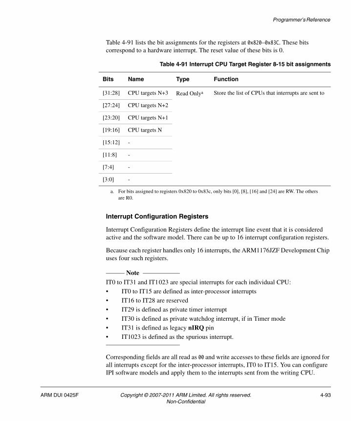
Programmer’s Reference
Table 4-91 lists the bit assignments for the registers at 0x820–0x83C. These bits correspond to a hardware interrupt. The reset value of these bits is 0.
Interrupt Configuration Registers
Interrupt Configuration Registers define the interrupt line event that it is considered active and the software model. There can be up to 16 interrupt configuration registers.
Because each register handles only 16 interrupts, the ARM1176JZF Development Chip uses four such registers.
Note IT0 to IT31 and IT1023 are special interrupts for each individual CPU:
• IT0 to IT15 are defined as inter-processor interrupts
• IT16 to IT28 are reserved
• IT29 is defined as private timer interrupt
• IT30 is defined as private watchdog interrupt, if in Timer mode
• IT31 is defined as legacy nIRQ pin
• IT1023 is defined as the spurious interrupt.
Corresponding fields are all read as 00 and write accesses to these fields are ignored for all interrupts except for the inter-processor interrupts, IT0 to IT15. You can configure IPI software models and apply them to the interrupts sent from the writing CPU.
Table 4-91 Interrupt CPU Target Register 8-15 bit assignments
Bits Name Type Function
[31:28] CPU targets N+3 Read Onlya
a. For bits assigned to registers 0x820 to 0x83c, only bits [0], [8], [16] and [24] are RW. The others are R0.
Store the list of CPUs that interrupts are sent to
[27:24] CPU targets N+2
[23:20] CPU targets N+1
[19:16] CPU targets N
[15:12] -
[11:8] -
[7:4] -
[3:0] -
ARM DUI 0425F Copyright © 2007-2011 ARM Limited. All rights reserved. 4-93Non-Confidential

Programmer’s Reference
These interrupts are aliased. An additional field in the Interrupt Acknowledge Register specifies the requesting processor.
Figure 4-40 shows the bit assignments for the Interrupt Configuration Register 0.
Figure 4-40 Interrupt Configuration Register 0 bit assignments
Table 4-92 lists the bit definition for the register at 0xC00.
31 30 29 28 27 26 25 24 23 22 21 20 19 18 17 16 15 14 13 12 11 10 9 8 7 6 5 4 3 2 1 0
ITnITn+1ITn+2ITn+3ITn+4ITn+5ITn+6ITn+7ITn+8ITn+9
ITn+10ITn+11ITn+12ITn+13ITn+14ITn+15
Table 4-92 Interrupt Configuration Register 0 bit definition
Bits Name Type Function
[31:30] ITn+15 Read/Write Configure software model for all 16 IPIs
[29:28] ITn+14
[27:26] ITn+13
[25:24] ITn+12
[23:22] ITn+11
4-94 Copyright © 2007-2011 ARM Limited. All rights reserved. ARM DUI 0425FNon-Confidential

Programmer’s Reference
You can configure the software model of the interrupts applied to in this register, but not the edge and level configuration. The testmask of this register, for example, for PMAP testing, is 0x55555555.
Table 4-94 and Table 4-94 list the encoding for the individual ITn bits.
[21:20] ITn+10 Read/Write Configure software model for all 16 IPIs
[19:18] ITn+9
[17:16] ITn+8
[15:14] ITn+7
[13:12] ITn+6
[11:10] ITn+5
[9:8] ITn+4
[7:6] ITn+3
[5:4] ITn+2
[3:2] ITn+1
[1:0] ITn
Table 4-93 IT[0] interrupt definition encoding
ITn[0] Description
0 Interrupt line uses the N-NN software model
1 Interrupt line uses the 1-N software model
Table 4-94 IT[1] interrupt definition encoding
ITn[1] Description
0 Interrupt line is considered as level HIGH active
1 Interrupt line is considered as rising edge sensitive
Table 4-92 Interrupt Configuration Register 0 bit definition (continued)
Bits Name Type Function
ARM DUI 0425F Copyright © 2007-2011 ARM Limited. All rights reserved. 4-95Non-Confidential

Programmer’s Reference
Figure 4-41 on page 4-96 shows the bit assignments for the Interrupt Configuration Register 1.
Figure 4-41 Interrupt Configuration Register 1 bit assignments
31 30 29 28 27 26 25 24 23 22 21 20 19 18 17 16 15 14 13 12 11 10 9 8 7 6 5 4 3 2 1 0
ITnITn+1ITn+2ITn+3ITn+4ITn+5ITn+6ITn+7ITn+8ITn+9
ITn+10ITn+11ITn+12ITn+13ITn+14ITn+15
4-96 Copyright © 2007-2011 ARM Limited. All rights reserved. ARM DUI 0425FNon-Confidential
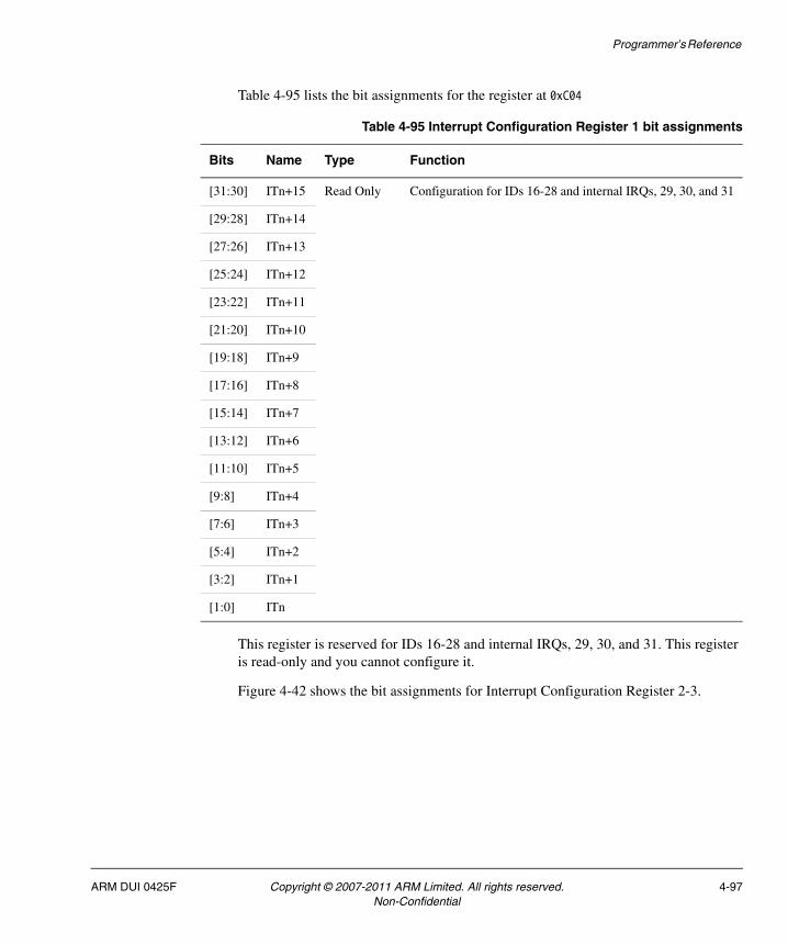
Programmer’s Reference
Table 4-95 lists the bit assignments for the register at 0xC04
This register is reserved for IDs 16-28 and internal IRQs, 29, 30, and 31. This register is read-only and you cannot configure it.
Figure 4-42 shows the bit assignments for Interrupt Configuration Register 2-3.
Table 4-95 Interrupt Configuration Register 1 bit assignments
Bits Name Type Function
[31:30] ITn+15 Read Only Configuration for IDs 16-28 and internal IRQs, 29, 30, and 31
[29:28] ITn+14
[27:26] ITn+13
[25:24] ITn+12
[23:22] ITn+11
[21:20] ITn+10
[19:18] ITn+9
[17:16] ITn+8
[15:14] ITn+7
[13:12] ITn+6
[11:10] ITn+5
[9:8] ITn+4
[7:6] ITn+3
[5:4] ITn+2
[3:2] ITn+1
[1:0] ITn
ARM DUI 0425F Copyright © 2007-2011 ARM Limited. All rights reserved. 4-97Non-Confidential

Programmer’s Reference
Figure 4-42 Interrupt Configuration Register 2-3 bit assignments
Table 4-96 lists the bit definition for the registers at 0xC08–0xC1C.
31 30 29 28 27 26 25 24 23 22 21 20 19 18 17 16 15 14 13 12 11 10 9 8 7 6 5 4 3 2 1 0
ITnITn+1ITn+2ITn+3ITn+4ITn+5ITn+6ITn+7ITn+8ITn+9
ITn+10ITn+11ITn+12ITn+13ITn+14ITn+15
Table 4-96 Interrupt Configuration Register 2-3 bit definition
Bits Name Type Function
[31:30] ITn+15 Read/Write Configure software model and edge and level for IDs 32-47, and 48-63
[29:28] ITn+14
[27:26] ITn+13
[25:24] ITn+12
[23:22] ITn+11
[21:20] ITn+10
[19:18] ITn+9
[17:16] ITn+8
[15:14] ITn+7
[13:12] ITn+6
[11:10] ITn+5
[9:8] ITn+4
[7:6] ITn+3 RW Configure software model and edge and level for IDs 32-47, and 48-63
[5:4] ITn+2
[3:2] ITn+1
[1:0] ITn
4-98 Copyright © 2007-2011 ARM Limited. All rights reserved. ARM DUI 0425FNon-Confidential

Programmer’s Reference
These two registers support hardware IRQs of ID 32-47, and 48-63. You can fully configure them.
Software Interrupt Register
The Software Interrupt Register is a write-only register that triggers an interrupt, identified by its own ID, to a list of CPUs. Figure 4-43 shows the bit assignments for this register.
Figure 4-43 Software Interrupt Register bit assignments
Table 4-97 lists the bit definition for the registers at 0xF00.
The CPU target list can be different from the one defined in the CPU Target List Register for the specified interrupt ID.
The Target List filter definition is:
• 00: Interrupt sent to CPUs listed in CPU Target List
• 01: CPU target list is ignored, interrupt is sent to all but the requesting CPU
• 10: CPU target list is ignored, interrupt is sent to the requesting CPU only
• 11: Reserved.
31 26 25 24 23 16 15 10 9 0
SBZ SBZ Interrupt IDCPU target list
Target list filter
Table 4-97 Software Interrupt Register bit definition
Bits Name Type Function
[31:26] SBZ Write Only Trigger specific interrupt---
[25:24] Target list filtera
a. Allowed values that trigger an interrupt on CPU0 are:target list filter = 0x00 and bit [0] of CPU target settarget list filter = 0x10.
[23:16] CPU target lista
[15:10] SBZ
[9:0] Interrupt ID Interrupt identifier
ARM DUI 0425F Copyright © 2007-2011 ARM Limited. All rights reserved. 4-99Non-Confidential

Programmer’s Reference
Note If you attempt to trigger an interrupt with an ID larger than the number of supported interrupts, or that references a CPU that is not present, there can be unpredictable effects in the interrupt distributor.
4.12.3 GIC CPU Interface
The CPU Interface registers are described in this section:
• GIC CPU Interface register summary on page 4-101
• Control register on page 4-101
• Priority Mask register on page 4-101
• Binary Point register on page 4-102
• Interrupt Acknowledge Register on page 4-103
• End of Interrupt (EOI) Register on page 4-104
• Running Interrupt Register on page 4-104
• Highest Pending Interrupt Register on page 4-104.
Note For the GIC in the development chip, the interrupt controller output goes to the nIRQ input of the CPU.
For the GICs in the FPGA, the output does not connect directly to the CPU:
• The nIRQ output of FPGA GIC0 goes to development chip GIC input 63 and TZIC input 31.
• The nFIQ output of FPGA GIC1 goes to development chip GIC input 62 and TZIC input 30.
4-100 Copyright © 2007-2011 ARM Limited. All rights reserved. ARM DUI 0425FNon-Confidential

Programmer’s Reference
GIC CPU Interface register summary
Table 4-98 shows the CPU interface registers.
Control register
Table 4-99 shows bit assignments for the CPU Interface Control register.
Priority Mask register
Use the Priority Mask to prevent interrupts from being sent to the CPU. The CPU interface asserts an interrupt request to the CPU if, and only if, the priority of the highest pending interrupt sent by the interrupt distributor is strictly higher than the mask value set in the Priority Mask Register.
Note The GICs in theFPGA do not connect directly to the CPU. The Mask register for FPGA GICs controls whether or not the interrupt inputs on the development chip TZIC and GIC are active.
Table 4-98 CPU interface registers
Name Offset Type Width Reset Description
Control 0x000 Read/Write 1 0x00000000 Control register
PriorityMask 0x004 Read/Write 4 0x00000000 Priority Mask register
BinaryPoint 0x008 Read/Write 3 0x00000003 Binary Point register
IrqAck 0x00C Read Only 13 0x000003FF Interrupt Ack register
EndIrq 0x010 Write Only 13 - End of Interrupt (EOI) register
RunningPriority 0x014 Read Only 4 0x000000FF Running Priority register
HighestPendingIrq 0x018 Read Only 13 0x000003FF Highest Pending Interrupt register
Table 4-99 CPU Interface Control register bit assignments
Bits Name Type Function
31:1 - Read/Write Reserved. SBZ
0 Enable Read/Write Enable
ARM DUI 0425F Copyright © 2007-2011 ARM Limited. All rights reserved. 4-101Non-Confidential

Programmer’s Reference
One consequence of the strict comparison is that lowest priority interrupt will never cause the assertion of interrupt request to the CPU. This allows an extra level of interrupt enabling. Although an interrupt can be pending, it will never be seen by the CPU. Table 4-100 shows bit assignments for the Priority Mask register.
Binary Point register
Binary point register is used to specify a certain number of bits to ignore in the priority comparison made in the CPU interface for pre-emption stack. Table 4-101 shows bit assignments for the Binary Pointer register.
Table 4-102 shows the meanings for Binary Point values:
Table 4-100 Priority Mask Register bit assignments
Bits Name Type Function
7:4 Priority Mask Read/Write Used to determine if the CPU interface asserts an interrupt request to CPU, if and only if the priority of the highest pending interrupt sent by the interrupt distributor is strictly higher than the mask set in this register.
Table 4-101 Binary Pointer Register bit assignments
Bits Name Type Function
31:3 SBZ/UNP Read/Write -
2:0 Binary Point Read/Write If this is set, ignore bits in priority comparison made in CPU interface for pre-emption stack.
Table 4-102 Binary Point value meanings
Value Meaning
000 Bits [7:1] of the priority are used to determine pre-emption
001 Bits [7:2] of the priority are compared for pre-emption.
010 Bits [7:3] of the priority are compared for pre-emption.
011 Bits [7:4] of the priority are compared for pre-emption.
100 Bits [7:5] of the priority are compared for pre-emption.
4-102 Copyright © 2007-2011 ARM Limited. All rights reserved. ARM DUI 0425FNon-Confidential

Programmer’s Reference
You can restrict the lowest value to any value from 0 to 4. If you attempt to specify a value less than the set minimum, the minimum value is used. This value can be read back to enable software discovery. At reset, the register takes its minimum supported value.
Interrupt Acknowledge Register
The Interrupt Acknowledge Register is a read-only register used by the CPU to determine the ID of the interrupt asserted by the CPU interface. Table 4-103 shows bit assignments for the Interrupt Acknowledge Register.
101 Bits [7:6] of the priority are compared for pre-emption.
110 Bits [7:7] of the priority are compared for pre-emption.
111 No pre-emption is performed. All bits of the priority are used for prioritization.
Table 4-102 Binary Point value meanings (continued)
Value Meaning
Table 4-103 Interrupt Acknowledge Register bit assignments
Bits Name Type Function
31:13 SBZ/RAZ Read Only -
12:10 CPU source ID CPU source ID value.
Depends on Interrupt ID field:
• If Interrupt ID field is 0 to 15, contains ID of the CPU that requested the IPI.
• In all other cases, CPU source ID field is read as zero. This can be ignored.
9:0 Interrupt ID Interrupt identifier
ARM DUI 0425F Copyright © 2007-2011 ARM Limited. All rights reserved. 4-103Non-Confidential

Programmer’s Reference
End of Interrupt (EOI) Register
This write-only register is used when the software finishes handling an interrupt. Table 4-104 shows bit assignments for the EOI Register.
Running Interrupt Register
This read-only register contains the priority level of the currently running interrupts on the CPU. Table 4-105 shows bit assignments for the Running Interrupt Register.
When no interrupt is running, defined as acknowledged by reading acknowledge register but not ended by writing to EOI register, the priority value read is 0xFF.
Highest Pending Interrupt Register
The Highest Pending Interrupt Register contains the Interrupt ID and CPU ID of the Highest Pending Interrupt for this CPU. If no interrupt is pending, the Interrupt ID returned is 0x3FF. This indicates a spurious interrupt.
Table 4-104 End of Interrupt Register bit assignments
Bits Name Type Function
31:13 SBZ/RAZ Write Only -
12:10 CPU source ID CPU source ID value.
Depends on Interrupt ID field:
• If Interrupt ID field is 0 to 15, contains ID of the CPU that requested the IPI.
• In all other cases, CPU source ID field is read as zero. This can be ignored.
9:0 Interrupt ID Interrupt identifier
Table 4-105 Running interrupt Register bit assignments
Bits Name Type Function
31:8 SBZ/UNP Read Only -
7:4 Priority Indicates priority level of the current running interrupt.
3:0 SBZ -
4-104 Copyright © 2007-2011 ARM Limited. All rights reserved. ARM DUI 0425FNon-Confidential

Programmer’s Reference
The format of the register is the same as the Interrupt Acknowledge Register. Table 4-106 shows bit assignments for the Highest Pending Interrupt Register.
4.12.4 GIC reserved register addresses
The offset of any particular register from the base address is fixed. Some register locations are reserved, and you must not used them during normal operation.
Registers corresponding to interrupts 0–31 are reserved for use by the processor.
Registers at the following locations are not used in this implementation of the GIC distributor:
• 0x008
• 0x0FF
• 0x108- 0x17C
• 0x188 - 0x1FF
• 0x208 - 27C
• 0x288 - 0x2FF
• 0x308 - 0x3FF
• 0x440 - 0x7FF
• 0x840 - 0xBFF
• 0xC10 - 0xDFF.
Table 4-106 Highest Pending interrupt Register bit assignments
Bits Name Type Function
31:13 SBZ/RAZ Write Only -
12:10 CPU Source ID CPU source ID value.
Depends on Interrupt ID field:
• If Interrupt ID field is 0 to 15, contains ID of the CPU that requested the IPI.
• In all other cases, CPU source ID field is read as zero. This can be ignored.
9:0 Interrupt ID Interrupt identifier
ARM DUI 0425F Copyright © 2007-2011 ARM Limited. All rights reserved. 4-105Non-Confidential

Programmer’s Reference
4.13 Level 2 Cache Controller
The L2CC has 128KB of unified cache that is clocked 1:1 with the core I and R/D buses.
Table 4-107 L2CC implementation in development chip
Property Value
Location ARM1176JZF-S development chip
Memory base address 0x10110000
Interrupt 45 on development chip GIC (13 TZIC)
Release version ARM L220 (pre-release version)
Reference documentation L220 Cache Controller Technical Reference Manual
4-106 Copyright © 2007-2011 ARM Limited. All rights reserved. ARM DUI 0425FNon-Confidential
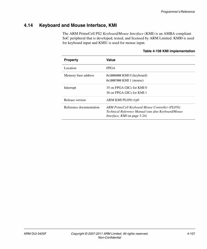
Programmer’s Reference
4.14 Keyboard and Mouse Interface, KMI
The ARM PrimeCell PS2 Keyboard/Mouse Interface (KMI) is an AMBA compliant SoC peripheral that is developed, tested, and licensed by ARM Limited. KMI0 is used for keyboard input and KMI1 is used for mouse input.
Table 4-108 KMI implementation
Property Value
Location FPGA
Memory base address 0x10006000 KMI 0 (keyboard)
0x10007000 KMI 1 (mouse)
Interrupt 35 on FPGA GICs for KMI 0
36 on FPGA GICs for KMI 1
Release version ARM KMI PL050 r1p0
Reference documentation ARM PrimeCell Keyboard Mouse Controller (PL050) Technical Reference Manual (see also Keyboard/Mouse Interface, KMI on page 3-24)
ARM DUI 0425F Copyright © 2007-2011 ARM Limited. All rights reserved. 4-107Non-Confidential
Programmer’s Reference
4.15 MultiMedia Card Interfaces, MCI
The PrimeCell Multimedia Card Interface (MCI) is an AMBA compliant SoC peripheral that is developed, tested, and licensed by ARM Limited.
Table 4-109 MCI implementation
Property Value
Location FPGA
Memory base address 0x10005000
Interrupt 33 on FPGA GICs for MCI
Release version ARM MCI PL180 r1p0
Reference documentation ARM PrimeCell Multimedia Card Interface (PL180) Technical Reference Manual.
4-108 Copyright © 2007-2011 ARM Limited. All rights reserved. ARM DUI 0425FNon-Confidential

Programmer’s Reference
4.16 PCI controller
The PCI controller is implemented in the FPGA and controls the interface to the PCI bus.
The PCI slave bridge connected to AXI M recognizes addresses 0x60000000 to 0x6FFFFFFF as being intended for a target within the PCI address space of the memory map, and passes accesses within this region to the PCI bus. The PCI master bridge connected to the PCI bus passes accesses to the AXI S bus.
Table 4-110 PCI controller implementation
Property Value
Location FPGA
Memory base address • 0x10019000 map and control registers
• 0x60000000–0x60FFFFFF Self configuration region
• 0x61000000–0x61FFFFFF PCI configuration region
• 0x62000000–0x62FFFFFF PCI I/O
• 0x63000000–0x63FFFFFF PCI memory region 0
• 0x64000000–0x67FFFFFF PCI memory region 1
• 0x68000000–0x6FFFFFFF PCI memory region 2
Interrupt No interrupts from PCI controller
47on FPGA GICs for external PCI slot number 3
46 on FPGA GICs for external PCI slot number 2
45 on FPGA GICs for external PCI slot number 1
44 on FPGA GICs for external PCI slot number 0
Note The PB1176JZF-S cannot generate an interrupt to the PCI bus.
This is a departure from the PCI bus specification.
Release version Custom logic (Xilinx)
Reference documentation PCI v2.2 Specification (see the PCI SIG web site at www.pcisig.com) See also Table 4-112 on page 4-110, PCI interface on page 3-27, and Appendix D PCI Backplane and Enclosure)
ARM DUI 0425F Copyright © 2007-2011 ARM Limited. All rights reserved. 4-109Non-Confidential

Programmer’s Reference
There are windows that provide access from the AXI master bus to the PCI expansion bus are listed in Table 4-111.
4.16.1 Control registers
The SYS_PCICTL, PCI_SELFID, and PCI_FLAGS control the operation of the PCI bus and provide status information. The PCI_IMAPx and PCI_SMAPx registers define the address translation values for the PCI I/O, PCI configuration, and PCI memory windows. See Table 4-112.
Table 4-111 PCI bus memory map for AXI M bridge
Usage Size AXI master address
PCI self config 16MB 0x60000000–0x60FFFFFF
PCI config 16MB 0x61000000–0x61FFFFFF
PCI I/O 16MB 0x62000000–0x62FFFFFF
PCI memory region 0 16MB 0x63000000–0x63FFFFFF
PCI memory region 1 256MB 0x64000000–0x67FFFFFF
PCI memory region 2 256MB 0x68000000–0x6FFFFFFF
Table 4-112 PCI controller registers
Address Name Access Description
0x10000044 SYS_PCICTL R/W Read returns a HIGH in bit 0 if a PCI board is present in the expansion backplane. (See PCI Control Register, SYS_PCICTL on page 4-50.)
0x10019000 PCI_IMAP0 R/W Translates address bits [31:24] from baseboard to PCI region 0.
0x10019004 PCI_IMAP1 R/W Translates address bits [31:26] from baseboard to PCI region 1.
0x10019008 PCI_IMAP2 R/W Translates address bits [31:27] from baseboard to PCI region 2.
0x1001900C PCI_SELFID R/W Slot location of the PB1176JZF-S.
0x10019010 PCI_FLAGS R/W Master and target abort flags
0x10019014 PCI_SMAP0 R/W Translates address bits [31:28] from PCI to baseboard region 0.
0x10019018 PCI_SMAP1 R/W Translates address bits [31:28] from PCI to baseboard region 1.
0x1001901C PCI_SMAP2 R/W Translates address bits [31:28] from PCI to baseboard region 2.
4-110 Copyright © 2007-2011 ARM Limited. All rights reserved. ARM DUI 0425FNon-Confidential

Programmer’s Reference
PCI_IMAPx registers
The registers remap high-order memory address bits for the PCI regions. Figure 4-44. shows the PCI_IMAP2 register contains 0x8 and this is used for the four high bits of the PCI address bus.
Figure 4-44 AXI M to PCI mapping
The map register formats are listed in Table 4-118 on page 4-114, Table 4-114, and Table 4-115 on page 4-112.
PCI bus address
PCI_IMAP0 register
AXI M address
61
PCI decode
Address bits [27:0]
87 Address bits [27:0]
0x61234567
0x87234567
87
Table 4-113 PCI_IMAP0 register format
Bits Description
[31:10] Reserved. Use read-modify-write to preserve value.
[9:0] Contains the value to use for bits [31:24] of the PCI address for accesses to this region.
Table 4-114 PCI_IMAP1 register format
Bits Description
[31:7] Reserved. Use read-modify-write to preserve value.
[6:0] Contains the value to use for bits [31:26] of the PCI address for accesses to this region.
ARM DUI 0425F Copyright © 2007-2011 ARM Limited. All rights reserved. 4-111Non-Confidential

Programmer’s Reference
PCI_SELFID register
Writing the slot location of the PB1176JZF-S into this register enables normal configuration accesses to return information on the PB1176JZF-S. That is, normal configuration accesses to this slot position are converted automatically into self configuration accesses.
Figure 4-45 shows the register bit assignments.
Figure 4-45 PCI_SELFID register
Table 4-116 lists the register bit assignments.
Table 4-115 PCI_IMAP2 register format
Bits Description
[31:6] Reserved. Use read-modify-write to preserve value.
[5:0] Contains the value to use for bits [31:27] of the PCI address for accesses to this region.
Table 4-116 PCI_SELFID register format
Bits Description
[31:5] Reserved. Use read-modify-write to preserve value.
[4:0] Contains the slot location of the PB1176JZF-S on the PCI backplane.
4-112 Copyright © 2007-2011 ARM Limited. All rights reserved. ARM DUI 0425FNon-Confidential

Programmer’s Reference
PCI_FLAGS register
This read-only register returns status information about abort conditions on the PCI bus. Figure 4-47 on page 4-114 shows the register bit assignments.
Figure 4-46 PCI_FLAGS register
Table 4-42 on page 4-50 lists the register bit assignments.
Table 4-117 PCI_FLAGS register format
Bits Description
[31:2] Reserved.
[1] Target abort flag. The bit value is the same as bit 38 of the Command Status Register in the Xilinx PCI controller. This bit position is reserved for future use.
[0] Master abort flag. The bit value is the same as bit 39 of the Command Status Register in the Xilinx PCI controller. This bit is HIGH if an error occurred while the PB1176JZF-S was operating as a master.
ARM DUI 0425F Copyright © 2007-2011 ARM Limited. All rights reserved. 4-113Non-Confidential
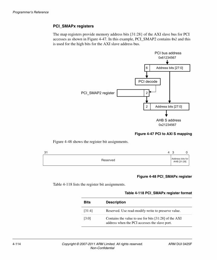
Programmer’s Reference
PCI_SMAPx registers
The map registers provide memory address bits [31:28} of the AXI slave bus for PCI accesses as shown in Figure 4-47. In this example, PCI_SMAP2 contains 0x2 and this is used for the high bits for the AXI slave address bus.
Figure 4-47 PCI to AXI S mapping
Figure 4-48 shows the register bit assignments.
Figure 4-48 PCI_SMAPx register
Table 4-118 lists the register bit assignments.
PCI bus address
PCI_SMAP2 register
AHB S address
PCI decode
2
Address bits [27:0]
6 Address bits [27:0]
0x21234567
0x61234567
2
Table 4-118 PCI_SMAPx register format
Bits Description
[31:4] Reserved. Use read-modify-write to preserve value.
[3:0] Contains the value to use for bits [31:28] of the AXI address when the PCI accesses the slave port.
4-114 Copyright © 2007-2011 ARM Limited. All rights reserved. ARM DUI 0425FNon-Confidential
Programmer’s Reference
4.16.2 PCI configuration
This section describes how to configure the PCI controllers on the PB1176JZF-S and any PCI cards attached to the PCI backplane.
Locating the self-config header table
The slot positions for PCI cards are numbered from 11 to 31. The numbering is based on the address bit that connects to the IDSEL line. The base address for the PCI configuration header is determined as follows:
0x60000000 + ((slot position)<<11)
For example, if the PB1176JZF-S is put into slot C where PCI address bit 29 is connected to the IDSEL signal, then the base address for the PB1176JZF-S header table is at memory location:
0x60000000 + (29<<11) = 0x6000E800
The self-configuration addresses for the slot A, B, and C in the PCI backplane are listed in Table 4-119.
The base address for normal configuration is 0x61000000. The normal configuration addresses for the slot A, B, and C in the PCI backplane are listed in Table 4-119.
Table 4-119 PCI backplane configuration header addresses (self-config)
SlotAddress connected to IDSEL
Configuration header memory
C 29 0x6000E800–0x6000E83F
B 30 0x6000F000–0x6000F03F
A 31 0x6000F800–0x6000F83F
Table 4-120 PCI backplane configuration header addresses (normalconfiguration)
SlotAddress connected to IDSEL
Configuration header memory
C 29 0x6100E800–0x6100E83F
B 30 0x6100F000–0x6100F03F
A 31 0x6100F800–0x6100F83F
ARM DUI 0425F Copyright © 2007-2011 ARM Limited. All rights reserved. 4-115Non-Confidential

Programmer’s Reference
The contents of the PCI configuration header is listed in Table 4-121. The default values are those of the PB1176JZF-S.
The PCI backplane uses the top 3 bits of PCI address to determine whether that slot must respond to configuration cycles. When the PB1176JZF-S generates PCI configuration cycles by accessing the 0x60000000 or 0x61000000 region, the only one of the PCI cards responds.
Table 4-121 PCI configuration space header
Address offset
Configuration word functionDefault value
+0x00 Device ID Vendor ID 0x0300 0x10EE
+0x04 Status Command 0x0220 0x0000
+0x08 Class Code Rev ID 0x0B40 0x0000
+0x0C BIST (Reserved in PB1176JZF-S) Header Type Lat. timer Line Size (Reserved in PB1176JZF-S)
0x00 0x00 0x00 0x00
+0x10 Base Address Register 0 (I/O bytes) 0x00000001
+0x14 Base Address Register 1 (memory) 0x00000008
+0x18 Base Address Register 2 (memory) 0x00000008
+0x1C Base Address Register 3 (reserved in PB1176JZF-S) -
+0x20 Base Address Register 4 (reserved in PB1176JZF-S) -
+0x24 Base Address Register 5 (reserved in PB1176JZF-S) -
+0x28 Cardbus CIS Pointer (reserved in PB1176JZF-S) -
+0x2C Subsystem ID Subsystem Vendor ID 0x0000 0x0000
+0x30 Expansion ROM Base Address (Reserved in PB1176JZF-S) -
+0x34 Unused (Reserved in PB1176JZF-S) CapPtr 0x0000 0x0000
+0x38 (Reserved in PB1176JZF-S) -
+0x3C Max_Lat Min_Gnt Interrupt PinInterrupt line 0x00 0x00 0x01 0xFF
4-116 Copyright © 2007-2011 ARM Limited. All rights reserved. ARM DUI 0425FNon-Confidential
Programmer’s Reference
See the PCI v2.2 specification for more information on the configuration space header.
Configuring the PCI interface
To configure a PCI card in the expansion bus, first find the memory location that maps the PB1176JZF-S into the system:
1. Scan addresses 0x60000000 + (n<<11) to locate the PCI slot holding the PB1176JZF-S. The slot range for n is 11 to 31. If you are using the horizontal slot on the PCI expansion backplane, n is 29.
2. Write the value of n that indicates the slot position into the PCI_SELFID register.
3. Set bit 2 of the Command/Status Register (at offset +0x04) to enable the PB1176JZF-S to be initiator on the system. This enables initiator transfers.
4. Because the PCI_SELFID register now holds the slot number for the PB1176JZF-S, scanning the normal configuration space at 0x61000000 reveals all PCI cards in the backplane.
Perform normal configuration cycles on other slot positions to see what else is on the bus. Instead of the self config area at 0x60000000, use memory locations in Config area 0x61000000 + (n<<11), where n is 11 to 31. That is, scan:
0x61005800, 0x61006000, 0x61006800, and the next address until 0x6100f800.
5. The accesses return 0xFFFFFFFF if the slot is empty, or the device and vendor id for card present. (For the PB1176JZF-S, the device/vendor id is 0x030010EE.)
If a card is present, read the base address registers to determine how much and what type of memory is required by each of target boards found in the system.
6. Write to the base address registers in the header table to setup the PCI memory map and tell each target the PCI memory addresses they must respond to (see Table 4-121 on page 4-116).
7. Set the PCI control registers at 0x10019000 appropriately so an access to one of the three memory regions causes a PCI access to the correct PCI memory location.
Note An example of PCI scanning and configuration is provided as an example on the CD.
ARM DUI 0425F Copyright © 2007-2011 ARM Limited. All rights reserved. 4-117Non-Confidential

Programmer’s Reference
Limitations of the PCI interface
The following limitations apply to the PCI interface present on the PB1176JZF-S:
• The interface is 32-bit only.
• The initiator creates only single reads and writes. This is quite inefficient and results in low performance. It does, however, simplify the logic in the FPGA and enables 66MHz performance.
• The target issues a retry response for reads until the data is ready.
• The target issues a retry response for reads or writes when the fifo is full (target has a 512 deep FIFO, initiator fifo is 16 deep)
• If another master accesses the PB1176JZF-S and it responds with 'retry' or 'disconnect without data', then this access must repeated before any other master accesses to the PB1176JZF-S.
• The PB1176JZF-S breaks up burst transfers. It typically completes the first cycle and then responds with 'disconnect without data'. The initiator must then retry with the address that responded with the disconnect.
• The AXI to AHB bridge that is used on the FPGA does not support sparse burst transfers. That is, bursts where the WSTRB[7:0] lines are not all 1 for every beat in the burst. See, PrimeCell Infrastructure AMBA 3 AXI to AMBA 2 AHB Bridges (BP137) Technical Overview.
• Only three out of five configuration base registers are usable.
• Cardbus CIS Pointer and Expansion ROM configuration registers are not implemented.
• There is no support for BIST.
• The PB1176JZF-S cannot generate an interrupt to the PCI bus.
Note This is a departure from the PCI bus specification.
• The target only responds to some of the sixteen PCI bus commands, and initiator only creates six of the cycle types (see Table 4-122 on page 4-119).
4-118 Copyright © 2007-2011 ARM Limited. All rights reserved. ARM DUI 0425FNon-Confidential
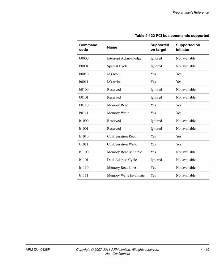
Programmer’s Reference
Table 4-122 PCI bus commands supported
Command code
NameSupported on target
Supported on initiator
b0000 Interrupt Acknowledge Ignored Not available
b0001 Special Cycle Ignored Not available
b0010 I/O read Yes Yes
b0011 I/O write Yes Yes
b0100 Reserved Ignored Not available
b0101 Reserved Ignored Not available
b0110 Memory Read Yes Yes
b0111 Memory Write Yes Yes
b1000 Reserved Ignored Not available
b1001 Reserved Ignored Not available
b1010 Configuration Read Yes Yes
b1011 Configuration Write Yes Yes
b1100 Memory Read Multiple Yes Not available
b1101 Dual Address Cycle Ignored Not available
b1110 Memory Read Line Yes Not available
b1111 Memory Write Invalidate Yes Not available
ARM DUI 0425F Copyright © 2007-2011 ARM Limited. All rights reserved. 4-119Non-Confidential
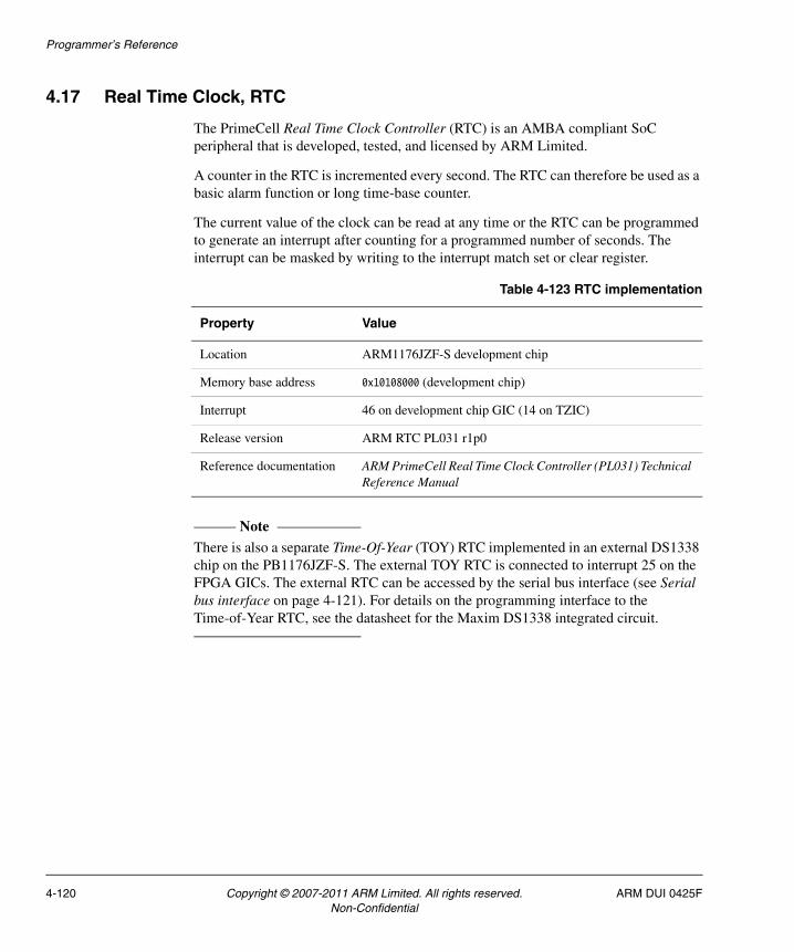
Programmer’s Reference
4.17 Real Time Clock, RTC
The PrimeCell Real Time Clock Controller (RTC) is an AMBA compliant SoC peripheral that is developed, tested, and licensed by ARM Limited.
A counter in the RTC is incremented every second. The RTC can therefore be used as a basic alarm function or long time-base counter.
The current value of the clock can be read at any time or the RTC can be programmed to generate an interrupt after counting for a programmed number of seconds. The interrupt can be masked by writing to the interrupt match set or clear register.
Note There is also a separate Time-Of-Year (TOY) RTC implemented in an external DS1338 chip on the PB1176JZF-S. The external TOY RTC is connected to interrupt 25 on the FPGA GICs. The external RTC can be accessed by the serial bus interface (see Serial bus interface on page 4-121). For details on the programming interface to the Time-of-Year RTC, see the datasheet for the Maxim DS1338 integrated circuit.
Table 4-123 RTC implementation
Property Value
Location ARM1176JZF-S development chip
Memory base address 0x10108000 (development chip)
Interrupt 46 on development chip GIC (14 on TZIC)
Release version ARM RTC PL031 r1p0
Reference documentation ARM PrimeCell Real Time Clock Controller (PL031) Technical Reference Manual
4-120 Copyright © 2007-2011 ARM Limited. All rights reserved. ARM DUI 0425FNon-Confidential

Programmer’s Reference
4.18 Serial bus interface
A serial bus interface is implemented in the FPGA. The registers shown in Table 4-125 control the serial bus and provides access to control signals on the two memory expansion boards and to the time-of-year clock.
Note SDA is an open-collector signal that is used for sending and receiving data. Set the output value HIGH before reading the current value.
Table 4-124 Serial bus implementation
Property Value
Location FPGA
Memory base address 0x10002000
Interrupt NA
Release version Custom logic
Reference documentation Serial bus interface on page 3-26, Appendix E Memory Expansion Boards, and the datasheet for the Dallas Maxim DS1338 Real Time Clock.
Table 4-125 Serial bus register
Address Name Access Description
0x10002000 SB_CONTROL Read only Read serial control bits:
Bit [0] is SCL
Bit [1] is SDA
0x10002000 SB_CONTROLS Write Set serial control bits:
Bit [0] is SCL
Bit [1] is SDA
0x10002004 SB_CONTROLC Write Clear serial control bits:
Bit [0] is SCL
Bit [1] is SDA
ARM DUI 0425F Copyright © 2007-2011 ARM Limited. All rights reserved. 4-121Non-Confidential

Programmer’s Reference
Software must manipulate the SCL and SDA bits directly to access the data in the three devices. The pre-defined eight-bit device addresses are listed in Table 4-126. See the \firmware\examples directory on the CD for example code for reading the memory expansion EEPROM.
Table 4-126 Serial bus device addresses
Device Write address Read address
Dynamic expansion E2PROM 0xA0 0xA1
Static expansion E2PROM 0xA2 0xA3
Time-of-year clock 0xD0 0xD1
4-122 Copyright © 2007-2011 ARM Limited. All rights reserved. ARM DUI 0425FNon-Confidential

Programmer’s Reference
4.19 Smart Card Interface, SCI
The PrimeCell Smart Card Interface (SCI) is an AMBA compliant SoC peripheral that is developed, tested, and licensed by ARM Limited.
The following key parameters are programmable:
• Smart Card clock frequency and communication baud rate
• protocol convention
• card activation and deactivation time
• check for maximum time for first character of Answer To Reset (ATR) reception
• check for maximum duration of ATR character stream
• check for maximum time for receipt of first character of data stream
• check for maximum time permitted ed between characters
• character and block guard time
• transmit and receive character retry and FIFO level
• clock start and stop time and inactive level.
See the self-test software that is supplied on the CD accompanying the PB1176JZF-S for a example of detecting a SIM card response to a reset.
Table 4-127 SCI implementation
Property Value
Location FPGA
Memory base address 0x1000E0000
Interrupt 37 on FPGA GICs
Release version ARM SCI PL131 r1p0
Reference documentation SCI PrimeCell PL131 Technical Reference Manual (see also Smart Card interface, SCI on page 3-25)
ARM DUI 0425F Copyright © 2007-2011 ARM Limited. All rights reserved. 4-123Non-Confidential

Programmer’s Reference
4.20 Synchronous Serial Port, SSP
The PrimeCell Synchronous Serial Port (SSP) is an AMBA compliant SoC peripheral that is developed, tested, and licensed by ARM Limited.
The SSP functions as a master or slave interface that enables synchronous serial communication with slave or master peripherals having one of the following:
• a Motorola SPI-compatible interface
• a Texas Instruments synchronous serial interface
• a National Semiconductor Microwire interface.
In both master and slave configurations, the PrimeCell SSP performs:
• parallel-to-serial conversion on data written to a transmit FIFO
• serial-to-parallel conversion and FIFO buffering of received data.
Interrupts are generated to:
• request servicing of the transmit and receive FIFO
• inform the system that a receive FIFO over-run has occurred
• inform the system that data is present in the receive FIFO.
The SSP controller can be shared with the following resources:
• If the LCD adaptor board is fitted with a touch screen, the controller interfaces to the SSP port to provide touch screen, keypad, LCD bias and analogue inputs. See the LCD adaptor board TSCI appendix for more details.
Note Use the SYS_CLCD register to control the SSP chip selects. See CLCD Control
Register, SYS_CLCD on page 4-50.
Table 4-128 SSP implementation
Property Value
Location ARM1176JZF-S development chip
Memory base address 0x1010B000.
Interrupt 49 on dev. chip GIC (17 on TZIC)
Release version ARM SSP PL022 r1p2
Reference documentation ARM PrimeCell Synchronous Serial Port Controller (PL022) Technical Reference Manual (see also Synchronous Serial Port, SSP on page 3-19)
4-124 Copyright © 2007-2011 ARM Limited. All rights reserved. ARM DUI 0425FNon-Confidential

Programmer’s Reference
• An offboard SSP device, such as an EEPROM, can be connected to expansion header J29. If you connect both the LCD adaptor board and the off board SSP device at the same time, ensure the correct SSP interface protocol is used when communicating with each device.
• Synthesized SSP peripherals in a RealView Logic Tile FPGA can be connected using the RealView Logic Tile expansion connectors. Disable the buffer with the RealView Logic Tile HDRY signal YL62 (nDRVINEN1) to avoid conflicts with the LCD adaptor board and expansion header.
ARM DUI 0425F Copyright © 2007-2011 ARM Limited. All rights reserved. 4-125Non-Confidential

Programmer’s Reference
4.21 Synchronous Static Memory Controller, SSMC
The PrimeCell Synchronous Static Memory Controller (SSMC) is an AMBA compliant SoC peripheral that is developed, tested, and licensed by ARM Limited.
The following key parameters are programmable for each SSMC memory bank:
• external memory width, 8, 16, or 32-bit
• burst mode operation
• write protection
• external wait control enable
• external wait polarity
• write WAIT states for static RAM devices
• read WAIT states for static RAM and ROM devices
• initial burst read WAIT state for burst devices
• subsequent burst read WAIT state for burst devices
• read byte lane enable control
• bus turn-around (idle) cycles
• output enable and write enable output delays.
Note To enable write access to the NOR flash (static chip select 1), set bit 0 of SYS_FLASH to HIGH. The default at power-on reset is LOW.
Table 4-129 SSMC implementation
Property Value
Location ARM1176JZF-S development chip
Memory base address 0x10111000
Interrupt NA
Release version ARM SSMC PL093 r0p4
Reference documentation ARM PrimeCell Static Memory Controller (PL093) Technical Reference Manual, Memory map on page 4-3, and Memory interface on page 3-17
4-126 Copyright © 2007-2011 ARM Limited. All rights reserved. ARM DUI 0425FNon-Confidential

Programmer’s Reference
4.21.1 Register values
Table 4-130 to Table 4-134 on page 4-128 lists the register values for the SSMC for typical operation of static memory devices and with a 35MHz system clock.
Note The platform.a library contains memory setup routines. See Building an application with the platform library on page F-10.
Table 4-130 Register values for NOR2
AddressName of SSMC register
Value Description
0x10111000 SMBIDCYR0 0x0 Idle Cycle Control Register for bank 0
0x10111004 SMBWSTRDR0 0x4 Read Wait State Control Reg bank 0
0x10111008 SMBWSTWRR0 0x2 Write Wait State Control Reg Bank 0
0x1011100C SMBWSTOENR0 0x1 Output Enable Assertion Delay 0
0x10111010 SMBWSTWENR0 0x1 Write Enable Assertion Delay 0
0x10111014 SMBCR0 0x303011 Control Register for memory bank 0
0x1011101C SMBWSTBRDR0 0x0 Burst Read Wait state Control Reg 0
Table 4-131 Register values for Intel flash, standard async read mode, no bursts
AddressName of SSMC register
Value Description
0x101110E0 SMBIDCYR7 0x0 Idle Cycle Control Register for bank 1
0x101110E4 SMBWSTRDR7 0x4 Read Wait State Control Reg bank 1
0x101110E8 SMBWSTWRR7 0x3 Write Wait State Control Reg Bank 1
0x101110EC SMBWSTOENR7 0x0 Output Enable Assertion Delay 1
0x101110F0 SMBWSTWENR7 0x1 Write Enable Assertion Delay 1
0x101110F4 SMBCR7 0x303021 Control Register for memory bank 1
0x101110FC SMBWSTBRDR7 0x0 Burst Read Wait state Control Reg 1
ARM DUI 0425F Copyright © 2007-2011 ARM Limited. All rights reserved. 4-127Non-Confidential

Programmer’s Reference
Table 4-132 Register values for Intel flash, async page mode
AddressName of SSMC register
Value Description
0x101110E0 SMBIDCYR7 0x0 Idle Cycle Control Register for bank 1
0x101110E4 SMBWSTRDR7 0x4 Read Wait State Control Reg bank 1
0x101110E8 SMBWSTWRR7 0x3 Write Wait State Control Reg Bank 1
0x101110EC SMBWSTOENR7 0x0 Output Enable Assertion Delay 1
0x101110F0 SMBWSTWENR7 0x1 Write Enable Assertion Delay 1
0x101110F4 SMBCR7 0x303521 Control Register for memory bank 1
0x101110FC SMBWSTBRDR7 0x0 Burst Read Wait state Control Reg 1
Table 4-133 Register values for Samsung SRAM
AddressName of SSMC register
Value Description
0x10111040 SMBIDCYR2 0x0 Idle Cycle Control Register for bank 2
0x10111044 SMBWSTRDR2 0x2 Read Wait State Control Reg bank 2
0x10111048 SMBWSTWRR2 0x2 Write Wait State Control Reg Bank 2
0x1011104C SMBWSTOENR2 0x0 Output Enable Assertion Delay 2
0x10111050 SMBWSTWENR2 0x1 Write Enable Assertion Delay 2
0x10111054 SMBCR2 0x303021 Control Register for memory bank 2
0x1011105C SMBWSTBRDR2 0x0 Burst Read Wait state Control Reg 2
Table 4-134 Register values for Spansion BDS640
AddressName of SSMC register
Value Description
0x10111060 SMBIDCYR3 0x0 Idle Cycle Control Register for bank 3
0x10111064 SMBWSTRDR3 0x3 Read Wait State Control Reg bank 3
0x10111068 SMBWSTWRR3 0x2 Write Wait State Control Reg Bank 3
4-128 Copyright © 2007-2011 ARM Limited. All rights reserved. ARM DUI 0425FNon-Confidential

Programmer’s Reference
0x1011106C SMBWSTOENR3 0x0 Output Enable Assertion Delay 3
0x10111070 SMBWSTWENR3 0x1 Write Enable Assertion Delay 3
0x10111074 SMBCR3 0x303021 Control Register for memory bank 3
0x1011107C SMBWSTBRDR3 0x0 Burst Read Wait state Control Reg 3
Table 4-135 Register values for Spansion LV256
AddressName of SSMC register
Value Description
0x10111080 SMBIDCYR4 0x0 Idle Cycle Control Register for bank 4
0x10111084 SMBWSTRDR4 0x4 Read Wait State Control Reg bank 4
0x10111088 SMBWSTWRR4 0x3 Write Wait State Control Reg Bank 4
0x1011108C SMBWSTOENR4 0x1 Output Enable Assertion Delay 4
0x10111090 SMBWSTWENR4 0x1 Write Enable Assertion Delay 4
0x10111094 SMBCR4 0x303121 Control Register for memory bank 4
0x1011109C SMBWSTBRDR4 0x1 Burst Read Wait state Control Reg 4
Table 4-134 Register values for Spansion BDS640 (continued)
AddressName of SSMC register
Value Description
ARM DUI 0425F Copyright © 2007-2011 ARM Limited. All rights reserved. 4-129Non-Confidential

Programmer’s Reference
4.22 System Controller
The system controller is an AMBA compliant SoC peripheral that is developed, tested, and licensed by ARM Limited.
The system controller in the ARM1176JZF-S development chip provides an interface to control the operation of the chip.
The system controller supports the following functionality:
• a system mode control state machine
• crystal and PLL control, system/peripheral clock control and status
• definition of system response to interrupts
• reset status capture and soft reset generation
• Watchdog and timer module clock enable generation
• remap control
• general purpose peripheral control registers.
Note There are also system control registers in the FPGA. See FPGA status and system control registers on page 4-37.
Table 4-136 System controller implementation
Property Value
Location ARM1176JZF-S development chip
Memory base address 0x10100000
Interrupt NA
Release version Custom implementation
Reference documentation See FPGA status and system control registers on page 4-37.
Note Bit 8 of the System controller register at 0x101E000 controls remapping of static memory devices to address 0x0. See also Memory map on page 4-3.
4-130 Copyright © 2007-2011 ARM Limited. All rights reserved. ARM DUI 0425FNon-Confidential
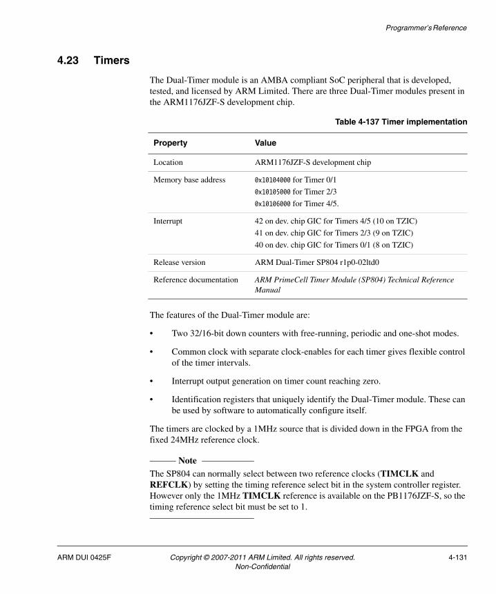
Programmer’s Reference
4.23 Timers
The Dual-Timer module is an AMBA compliant SoC peripheral that is developed, tested, and licensed by ARM Limited. There are three Dual-Timer modules present in the ARM1176JZF-S development chip.
The features of the Dual-Timer module are:
• Two 32/16-bit down counters with free-running, periodic and one-shot modes.
• Common clock with separate clock-enables for each timer gives flexible control of the timer intervals.
• Interrupt output generation on timer count reaching zero.
• Identification registers that uniquely identify the Dual-Timer module. These can be used by software to automatically configure itself.
The timers are clocked by a 1MHz source that is divided down in the FPGA from the fixed 24MHz reference clock.
Note The SP804 can normally select between two reference clocks (TIMCLK and REFCLK) by setting the timing reference select bit in the system controller register. However only the 1MHz TIMCLK reference is available on the PB1176JZF-S, so the timing reference select bit must be set to 1.
Table 4-137 Timer implementation
Property Value
Location ARM1176JZF-S development chip
Memory base address 0x10104000 for Timer 0/1
0x10105000 for Timer 2/3
0x10106000 for Timer 4/5.
Interrupt 42 on dev. chip GIC for Timers 4/5 (10 on TZIC)
41 on dev. chip GIC for Timers 2/3 (9 on TZIC)
40 on dev. chip GIC for Timers 0/1 (8 on TZIC)
Release version ARM Dual-Timer SP804 r1p0-02ltd0
Reference documentation ARM PrimeCell Timer Module (SP804) Technical Reference Manual
ARM DUI 0425F Copyright © 2007-2011 ARM Limited. All rights reserved. 4-131Non-Confidential
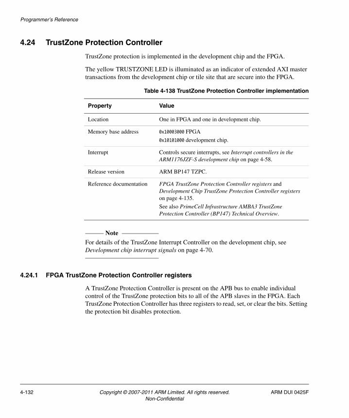
Programmer’s Reference
4.24 TrustZone Protection Controller
TrustZone protection is implemented in the development chip and the FPGA.
The yellow TRUSTZONE LED is illuminated as an indicator of extended AXI master transactions from the development chip or tile site that are secure into the FPGA.
Note For details of the TrustZone Interrupt Controller on the development chip, see Development chip interrupt signals on page 4-70.
4.24.1 FPGA TrustZone Protection Controller registers
A TrustZone Protection Controller is present on the APB bus to enable individual control of the TrustZone protection bits to all of the APB slaves in the FPGA. Each TrustZone Protection Controller has three registers to read, set, or clear the bits. Setting the protection bit disables protection.
Table 4-138 TrustZone Protection Controller implementation
Property Value
Location One in FPGA and one in development chip.
Memory base address 0x10003000 FPGA
0x10101000 development chip.
Interrupt Controls secure interrupts, see Interrupt controllers in the ARM1176JZF-S development chip on page 4-58.
Release version ARM BP147 TZPC.
Reference documentation FPGA TrustZone Protection Controller registers and Development Chip TrustZone Protection Controller registers on page 4-135.
See also PrimeCell Infrastructure AMBA3 TrustZone Protection Controller (BP147) Technical Overview.
4-132 Copyright © 2007-2011 ARM Limited. All rights reserved. ARM DUI 0425FNon-Confidential

Programmer’s Reference
The TZPCDECPROTx registers in the FPGA TrustZone Protection Controller are listed in Table 4-139.
Table 4-139 FPGA TrustZone Protection Controller registers
Register Address Access Description
TZPCDECPROT0Stat 0x10003800 Read-only Read status bits for devices listed in Table 4-140 on page 4-134.
TZPCDECPROT0Set 0x10003804 Write Set status bits and disable protection for devices listed in Table 4-140 on page 4-134.
If a bit is set to 1 in this register, the corresponding bit in the security status is set and non-secure access is enabled. Bits set to 0 do not affect the status.
TZPCDECPROT0Clr 0x10003808 Write Clear bits and enable protection. If a bit is set to 1 in this register, the corresponding bit in the security status is cleared and non-secure access is blocked. Bits set to 0 do not affect the status.
TZPCDECPROT1Stat 0x1000380C Read-only Read status bits for devices listed in Table 4-141 on page 4-134.
TZPCDECPROT1Set 0x10003810 Write Set status bits and disable protection. Bit values have the same effect as described for TZPCDECPROT0Set.
TZPCDECPROT1Clr 0x10003814 Write Clear bits and enable protection. Bit values have the same effect as described for TZPCDECPROT0Clr.
TZPCDECPROT2Stat 0x10003818 Read-only Read security status for devices listed in Table 4-142 on page 4-135.
TZPCDECPROT2Set 0x1000381C Write Set status bits and disable protection. Bit values have the same effect as described for TZPCDECPROT0Set.
TZPCDECPROT2Clr 0x10003820 Write Clear bits and enable protection. Bit values have the same effect as described for TZPCDECPROT0Clr.
TZPCDECPROT3Stat 0x10003824 Read-only Reserved.
TZPCDECPROT3Set 0x10003828 Write Reserved.
TZPCDECPROT3Clr 0x1000382C Write Reserved.
ARM DUI 0425F Copyright © 2007-2011 ARM Limited. All rights reserved. 4-133Non-Confidential

Programmer’s Reference
FPGA TZPCDECPROT0 register
The peripherals controlled by TZPCDECPROT0 are listed in Table 4-140:
FPGA TZPCDECPROT1 register
The peripherals controlled by TZPCDECPROT1 are listed in Table 4-141:
Table 4-140 FPGA TZPCDECPROT0x bit assignment
Bits Access Description
[31:8] Read/write Reserved
[7] Read/write KMI1
[6] Read/write KMI0
[5] Read/write MMCI
[4] Read/write AACI
[3] Read/write TZ Protection Controller on FPGA.
[2] Read/write Serial bus
[1] Read/write Sys Control
[0] Read/write Sys Registers
Table 4-141 FPGA TZPCDECPROT1x bit assignment
Bits Access Description
[31:8] Read/write Reserved
[7] Read/write RTC
[6] Read/write GPIO2
[5] Read/write GPIO1
[4] Read/write TIMER23
[3] Read/write TIMER01
[2] Read/write SCI
[1] Read/write UART4
[0] Read/write CHARLCD
4-134 Copyright © 2007-2011 ARM Limited. All rights reserved. ARM DUI 0425FNon-Confidential
Programmer’s Reference
FPGA TZPCDECPROT2 register
The peripherals controlled by TZPCDECPROT2 are listed in Table 4-142:
4.24.2 Development Chip TrustZone Protection Controller registers
A TrustZone Protection Controller implemented inside the development chip controls secure or non-secure access for internal RAM and the slaves and masters on the PL300 interconnect. The development chip TZPC registers are listed in Table 4-143:
Table 4-142 FPGA TZPCDECPROT2 register
Bits Access Description
[31:4] Read/write Reserved
[3] Read/write DAP ROM Table. Not implemented.
[2] Read/write GIC0
[1] Read/write Power Monitor
[0] Read/write PCI Controller
Table 4-143 Development chip TrustZone Protection Controller registers
Register Access Address Description
TZPCR0SIZE Read/Write 0x10101000 Protection for internal RAM on dev. chip.
TZPCDECPROT0Stat Read-only 0x10101800 Security status for slaves and masters listed in Table 4-144 on page 4-137.
TZPCDECPROT0Set Write 0x10101804 Set status bits and disable protection. If a bit is set to 1 in this register, the corresponding bit in the security status is set and non-secure access is allowed. Bits set to 0 do not affect the status.
TZPCDECPROT0Clr Write 0x10101808 Clear bits and enable protection. If a bit is set to 1 in this register, the corresponding bit in the security status is cleared and non-secure access is blocked. Bits set to 0 do not affect the status.
TZPCDECPROT1Stat Read-only 0x1010180C Read security status for slaves and masters listed in Table 4-145 on page 4-138.
ARM DUI 0425F Copyright © 2007-2011 ARM Limited. All rights reserved. 4-135Non-Confidential

Programmer’s Reference
TZPCR0SIZE register
Security for the internal RAM in the development chip is managed by the TZPCR0SIZE register.
The R0SIZE signals from the TZPC are connected directly to the TrustZone Memory Adapter for the on-chip 512KB RAM and define the secure RAM regions in 4KB increments from the RAM base address of 0x10300000:
• there is no secure region if all of the TZPCR0SIZE bits are clear
• the first 4KB of RAM is secure if you set TZPCR0SIZE to 0x00000001.
• the entire 512KB RAM is secure if you set bits[9:0] of TZPCR0SIZE to a value greater than or equal to 0x000000FF.
At reset, the entire RAM space is defined as secure.
Region R0 in Figure 4-49 on page 4-137 is the secure region for the internal RAM. Region R1 is non-secure and exists in the remaining region to the end of the memory block.
TZPCDECPROT1Set Write 0x10101810 Set status bits and disable protection. Bit values have the same effect as described for TZPCDECPROT0Set.
TZPCDECPROT1Clr Write 0x10101814 Clear bits and enable protection. Bit values have the same effect as described for TZPCDECPROT0Clr.
TZPCDECPROT2Stat Read-only 0x10101818 Read security status for slaves and masters listed in Table 4-146 on page 4-139.
TZPCDECPROT2Set Write 0x1010181C Set status bits and disable protection. Bit values have the same effect as described for TZPCDECPROT0Set.
TZPCDECPROT2Clr Write 0x10101820 Clear bits and enable protection. Bit values have the same effect as described for TZPCDECPROT0Clr.
Table 4-143 Development chip TrustZone Protection Controller registers (continued)
Register Access Address Description
4-136 Copyright © 2007-2011 ARM Limited. All rights reserved. ARM DUI 0425FNon-Confidential

Programmer’s Reference
Figure 4-49 Secure and non-secure internal RAM
TZPCDECPROT0x registers
The peripherals controlled by the TZPCDECPROT0x registers are listed in Table 4-144:
Size is equal to value in TZPCR0SIZE * 4K
Region R0Secure RAM
Region R1Non-secure RAM
Size is any memory left after defining the secure area:
512KB – R0
0x10300000
0x1037FFFF
Table 4-144 Development chip TZPCDECPROT0x bit assignment
Bits Access Description
[15] Read/write UART3
[14] Read/write UART2
[13] Read/write UART1
[12] Read/write UART0
[11] Read/write SSP
[10] Read/write GPIO
[9] Read/write DMC Configuration Port
[8] Read/write RTC
[7] Read/write Watchdog
[6] Read/write Timers 4/5
[5] Read/write Timers 2/3
[4] Read/write Timers 0/1
ARM DUI 0425F Copyright © 2007-2011 ARM Limited. All rights reserved. 4-137Non-Confidential

Programmer’s Reference
TZPCDECPROT1x registers
The peripherals controlled by the TZPCDECPROT1x registers are listed in Table 4-145:
Set the corresponding bit to disable protection for the associated peripheral or bus.
[3] Read/write IEC
[2] Read/write APC
[1] Read/write SBZ (unused)
[0] Read/write System Controller
Table 4-145 Development chip TZPCDECPROT1x bit assignment
Bits Access Description
[15:4] Read/write SBZ (Reserved)
[13] Read/write AXI ROM
[12] Read/write AXI Master Port
[11:8] Read/write DMC Chip Select 3–0
Note Because the DMC chip select pins are aliased, securing a block of the dynamic memory requires clearing both the chip select and the aliased chip select.
For example, clear both bit 10 and bit 8 to 1 to secure the lower block of memory.
[7:0] Read/write SMC Chip Select 7–0
Table 4-144 Development chip TZPCDECPROT0x bit assignment (continued)
Bits Access Description
4-138 Copyright © 2007-2011 ARM Limited. All rights reserved. ARM DUI 0425FNon-Confidential

Programmer’s Reference
TZPCDECPROT2x registers
The peripherals controlled by the TZPCDECPROT2x registers are listed in Table 4-146:
Table 4-146 Development chip TZPCDECPROT2
Bits Access Description
[15:5] Read/write SBZ (Reserved)
[7] Read/write Trust Zone Interrupt Controller
[6] Read/write CLCD Configuration Port
[5] Read/write CLCD Master Port
[4] Read/write AXI Slave Port
[3:0] Read/write AXI Master Port 3–0. Exported off chip
ARM DUI 0425F Copyright © 2007-2011 ARM Limited. All rights reserved. 4-139Non-Confidential

Programmer’s Reference
4.25 UART
The PrimeCell UART is an AMBA compliant SoC peripheral that is developed, tested, and licensed by ARM Limited. There are three UARTs in the ARM1176JZF-S development chip and one UART is in FPGA. The 24MHz reference clock to the UARTs come from the crystal oscillator that is part of OSC0.
You can program the following key parameters:
• communication baud rate, integer, and fractional parts
• number of data and stop bits
• parity mode
• FIFO enable and FIFO trigger levels
• UART or IrDA protocol
• hardware flow control.
Table 4-147 UART implementation
Property Value
Location ARM1176JZF-S development chip for UART 0-3
FPGA for UART4.
Memory base address 0x1010C000 for UART0
0x1010D000 for UART1
0x1010E000 for UART2
0x1010F000 for UART3
0x10009000 for UART4
Interrupt 50 on dev. chip GIC for UART0 (18 on TZIC)
51 on dev. chip GIC for UART1 (19 on TZIC)
52 on dev. chip GIC for UART2 (20 on TZIC)
53 on dev. chip GIC for UART3 (21 on TZIC)
38 on FPGA GICs for UART4
Release version ARM UART PL011 r1p3
Reference documentation ARM PrimeCell UART (PL011) Technical Reference Manual (see also UART interface on page 3-20).
4-140 Copyright © 2007-2011 ARM Limited. All rights reserved. ARM DUI 0425FNon-Confidential

Programmer’s Reference
4.25.1 PrimeCell Modifications
The PrimeCell UART varies from the industry-standard 16C550 UART device as follows:
• receive FIFO trigger levels are 1/8, 1/4, 1/2, 3/4, and 7/8
• the internal register map address space, and the bit function of each register differ
• the deltas of the modem status signals are not available
• 1.5 stop bits not available (1 or 2 stop bits only are supported)
• no independent receive clock.
ARM DUI 0425F Copyright © 2007-2011 ARM Limited. All rights reserved. 4-141Non-Confidential

Programmer’s Reference
4.26 USB interface
The USB interface is provided by an external NXP ISP1761 USB 2.0 controller that provides a standard USB host controller and an On-The-Go (OTG) dual role device controller. The USB host has one or two downstream ports. The OTG can function as either a host or slave device.
The ISP1761 has the following features:
• fully compliant to the USG On-The-Go specification
• configurable number of downstream and upstream hosts or functions
• USB host is USB 2.0 compliant and supports 12Mb/s and 1.5Mb/s
• programmable interrupts
• 4KB on-chip RAM.
The ISP1761 register base addresses are shown in Table 4-149.
Table 4-148 USB implementation
Property Value
Location Board (an ISP1761 chip).
Memory base address 0x3B000000 on static CS6, the registers in the ISP1761 are memory-mapped into the static memory area.
Interrupt 43 on FPGA GICs
Release version Custom interface in FPGA to external ISP1761 controller
Reference documentation NXP ISP1761 Data Sheet (see also USB interface on page 3-27 and test program supplied on the CD).
Table 4-149 USB controller base address
Address Description
0x3B020000 Chip-level register bank
0x3B020080 Host controller register bank
0x3B020100 Function controller register bank
4-142 Copyright © 2007-2011 ARM Limited. All rights reserved. ARM DUI 0425FNon-Confidential

Programmer’s Reference
4.27 Watchdog
The PrimeCell Watchdog module is an AMBA compliant SoC peripheral developed, tested and licensed by ARM Limited. The Watchdog module consists of a 32-bit down counter with a programmable timeout interval that has the capability to generate an interrupt and a reset signal on timing out. It is intended to be used to apply a reset to a system in the event of a software failure.
Note The Watchdog counter is disabled if the core is in debug state.
The following Watchdog module parameters are programmable:
• interrupt generation enable/disable
• interrupt masking
• reset signal generation enable/disable
• interrupt interval.
Table 4-150 Watchdog implementation
Property Value
Location ARM1176JZF-S development chip
Memory base address 0x10107000
Interrupt 32 on dev. chip GIC (0 on TZIC)
Release version ARM WDOG SP805 r2p0
Reference documentation ARM PrimeCell Watchdog Controller (SP805) Technical Reference Manual
ARM DUI 0425F Copyright © 2007-2011 ARM Limited. All rights reserved. 4-143Non-Confidential

Programmer’s Reference
4-144 Copyright © 2007-2011 ARM Limited. All rights reserved. ARM DUI 0425FNon-Confidential
Appendix A Signal Descriptions
This appendix provides a summary of signals present on the PB1176JZF-S connectors. It contains the following sections:
• Synchronous Serial Port interface on page A-2
• Smart Card interface on page A-3
• UART interface on page A-5
• USB interface on page A-6
• Audio CODEC interface on page A-7
• MMC and SD flash card interface on page A-9
• CLCD DVI display interface on page A-11
• GPIO interface on page A-12
• Keyboard and mouse interface on page A-13
• Ethernet interface on page A-14
• RealView Logic Tile header connectors on page A-15
• Test and debug connections on page A-16.
For more information on connectors used on the PB1176JZF-S, see the parts list spreadsheet in the CD schematics directory.
ARM DUI 0425F Copyright © 2007-2011 ARM Limited. All rights reserved. A-1Non-Confidential

Signal Descriptions
A.1 Synchronous Serial Port interface
Figure A-1 shows the signals on the expansion SSP interface connector J29.
Figure A-1 SSP expansion interface
The signals associated with the SSP are shown in Table A-1.
Table A-1 SSP signal assignment
Signal name Description
SSPCLKOUT Clock output from controller
SSPCLKIN Clock input to controller
nSSPCTLOE Control output enable control
nSSPOE Data output enable control
SSPFSSOUT Frame sync output
SSPFSSIN Frame sync input
SSPTXD Data output
SSPRXD Data input
SSPnCS Chip select
A-2 Copyright © 2007-2011 ARM Limited. All rights reserved. ARM DUI 0425FNon-Confidential

Signal Descriptions
A.2 Smart Card interface
The PB1176JZF-S contains a Smart Card SIM socket.
The signals associated with the SCI connector J33 are listed in Table A-2.
Figure A-2 Smartcard contacts assignment
Figure A-2 shows the signal assignment of a Smart Card. Pins 4 and 8 are not connected and are omitted on some cards.
The SIM card is inserted into the SIM card socket with the contacts face down.
Table A-2 Smartcard connector signal assignment
Pin Signal Description
1 SC_VCC Card power (1.8V, 3.3V, or 5V)
2 SC_RST Reset to card
3 SC_CLK Clock to or from card
4 NC -
5 GND Ground
6 SC_VCC Card power (1.8V, 3.3V, or 5V)
7 SC_IO Serial data to or from the card
8 NC -
SW1 nSCIDETECT Card detect signal from switch in socket (not present on J25 and J26)
SC_IOnSC_RSTSC_CLK
SC_VCC (1.8, 3.3 or 5V) GND1234
5678
SC_VCC
ARM DUI 0425F Copyright © 2007-2011 ARM Limited. All rights reserved. A-3Non-Confidential

Signal Descriptions
Table A-3 lists the signals on the SCI expansion connector. The signals on the expansion connector are use 3.3V logic levels. The SCIVCCEN signal disables the signals and power supply to SCI connector J33.
Figure A-3 SCI expansion connector J29
Table A-3 Signals on SCI expansion connector
Pin Signal name
1 Ground
2 SCIFCB
3 SCIDATA
4 nSCIDETECT
5 SC_VCC (card power)
6 nSCICARDRST (reset)
7 SCICLK (clock)
8 NC
SCICLK
SCIFCB
SCIDATA
NC
GND SC_VCC
nSCICARDRST
nSCIDETECT
51
2
3
4
6
7
8
A-4 Copyright © 2007-2011 ARM Limited. All rights reserved. ARM DUI 0425FNon-Confidential

Signal Descriptions
A.3 UART interface
The PB1176JZF-S provides five serial transceivers. All use 9-pin D-type male connectors except for UART3 (J28) that uses a standard 10-pin 2.54mm header connector.
Figure A-4 shows the D-type connector and Table A-4 shows the signal assignment for the D-type and header connectors. The pinout shown in Figure A-4 is configured as a Data Communications Equipment (DCE) device.
Figure A-4 Serial connector for J26A, J26B, J27A, and J27B
1 26 7 8 9
3 4 5
Table A-4 Serial plug signal assignment
PinUART0 J26A (top)
UART1 J26B (bottom)
UART2 J27A (top)
UART3 J28 (10-pin header)
UART4 J27B (bottom)
1 SER0_DCD NC NC NC NC
2 SER0_RX SER1_RX SER2_RX SER3_DSR SER4_RX
3 SER0_TX SER1_TX SER2_TX SER3_RX SER4_TX
4 SER0_DTR SER1_DTRa SER2_DTRa SER3_RTSa SER4_DTR
5 SER0_GND SER1_GND SER2_GND SER3_TX SER4_GND
6 SER0_DSR SER1_DSR SER2_DSR SER3_CTS SER4_DSR
7 SER0_RTS SER1_RTSa SER2_RTSa SER3_DTRa SER4_RTS
8 SER0_CTS SER1_CTS SER2_CTS NC SER4_CTS
9 SER0_RI NC NC GND NC
10 - - - NC -
a. The signals SER1_DTR, SER2_DTR, and SER3_DTR are connected to the corresponding SER1_DSR, SER2_DSR, and SER3_DSR signals. These signals cannot be set or read under program control.
ARM DUI 0425F Copyright © 2007-2011 ARM Limited. All rights reserved. A-5Non-Confidential

Signal Descriptions
A.4 USB interface
USB2 and USB3 provide USB host interfaces and connect through the type A connector J19.
USB1 provides an OTG interface and connects through the OTG connector J18.
Note For a full description of the USB signals see the datasheet for the TransDimension ISP1761 USB controller.
Figure A-5 shows the USB connectors.
Figure A-5 USB interfaces
Table A-5 USB signals
Pin J18 USB OTG J19 dual USB
1 VBUSP1 (power) VBUSP2 (power)
2 DM1 DM3
3 DP1 DP3
4 ID GND2
5 GND1 VBUSP3
6 - DM2
7 - DP2
8 - GND3
USB11 2 3 4 5
1 2 3 4
5 6 7 8
USB3
USB2
A-6 Copyright © 2007-2011 ARM Limited. All rights reserved. ARM DUI 0425FNon-Confidential

Signal Descriptions
A.5 Audio CODEC interface
The PB1176JZF-S provides three jack connectors that enable you to connect to the microphone and auxiliary inputs, and line level output on the CODEC. Figure A-6 shows the pinouts of the sockets.
Note A link on the board enables bias voltage to be applied to the microphone (see Advanced Audio Codec Interface, AACI on page 3-24).
Figure A-6 Audio connectors
The signals associated with the audio CODEC interface are also assigned to connector J45, the AACI expansion socket pins, as shown in Table A-6.
6 AGND5 AMP_L
4 AMP_R
7 CODEC_LINE_IN_L
1 CODEC_LINE_IN_R
3 AGND
5 CODEC_MIC11 AGND
2 CODEC_MIC2
Microphone(J4)
Line in(J3 bottom)
Line out(J3 top)
2 AGND8 AGND
Table A-6 Audio CODEC expansion connector signals
Pin number
Signal name Description
1 AACIBITCLK Clock from the CODEC to the AACI
2 AACISYNC Frame synchronization signal from the AACI
3 AACISDATAIN Serial data from the CODEC to the AACI
ARM DUI 0425F Copyright © 2007-2011 ARM Limited. All rights reserved. A-7Non-Confidential

Signal Descriptions
Figure A-7 shows the pinouts of the AACI expansion connector.
Figure A-7 AACI expansion connector
4 AACI_RESET Reset signal from the AACI to the CODEC
5 AACISDATAOUT Serial data from the AACI to the CODEC
6 GND Signal ground
Table A-6 Audio CODEC expansion connector signals (continued)
Pin number
Signal name Description
AACISDATAIN
AACIRESET
AACISDATAOUT
GND5
6
3
4
AACIBITCLK2
AACISYNC1
2
A-8 Copyright © 2007-2011 ARM Limited. All rights reserved. ARM DUI 0425FNon-Confidential

Signal Descriptions
A.6 MMC and SD flash card interface
The MMC/SD card sockets provides nine pins that connect to the card when it is inserted into the socket. Figure A-8 shows the pin numbering and signal assignment. In addition, the socket contains switches that are operated by card insertion and provide signaling on the nCARDIN and WPROT signals.
Figure A-8 MMC/SD card socket pin numbering
The MMC card uses seven pins, but the SD card uses all nine pins. The additional pins are located as shown in Figure A-8 with pin 9 next to pin 1 and pins 7 and 8 spaced more closely together than the other pins. Figure A-9 shows an MCI card, with the contacts face up.
Figure A-9 MMC card
DATA3CMD
Ground
VDDClock
DATA0DATA1
DATA2
Card in
Write protect
876543219
Ground
Ground
Ground
1 2 3 4 5 6 7
ARM DUI 0425F Copyright © 2007-2011 ARM Limited. All rights reserved. A-9Non-Confidential

Signal Descriptions
Table A-7 lists the signal assignments.
Insert and remove the card as follows:
Insertion Insert the card into the socket with the contacts face down. Cards are normally labeled on the top surface with an arrow to indicate correct insertion.
Removal Remove the card by gently pressing it into the socket. It springs back and can be removed. Removing the card in this way ensures that the card detection switches within the socket operate correctly.
Table A-7 Multimedia Card interface signals
Pin SignalFunction SD widebus mode
Function MCI
1 MCIDATA3 Data Chip select
2 MCICMD Command/response Data in
3 GND Ground Ground
4 MCIVDD Supply voltage Supply voltage
5 MCICLK Clock Clock
6 GND Ground Ground
7 MCIDATA0 Data 0 Data out
8 MCIDATA1 Data 1 NC
9 MCIDATA2 Data 2 NC
10 (DET A) CARDIN Card insertion detect Card insertion detect
11 (DET B) WPROT Write protect status Write protect status
A-10 Copyright © 2007-2011 ARM Limited. All rights reserved. ARM DUI 0425FNon-Confidential
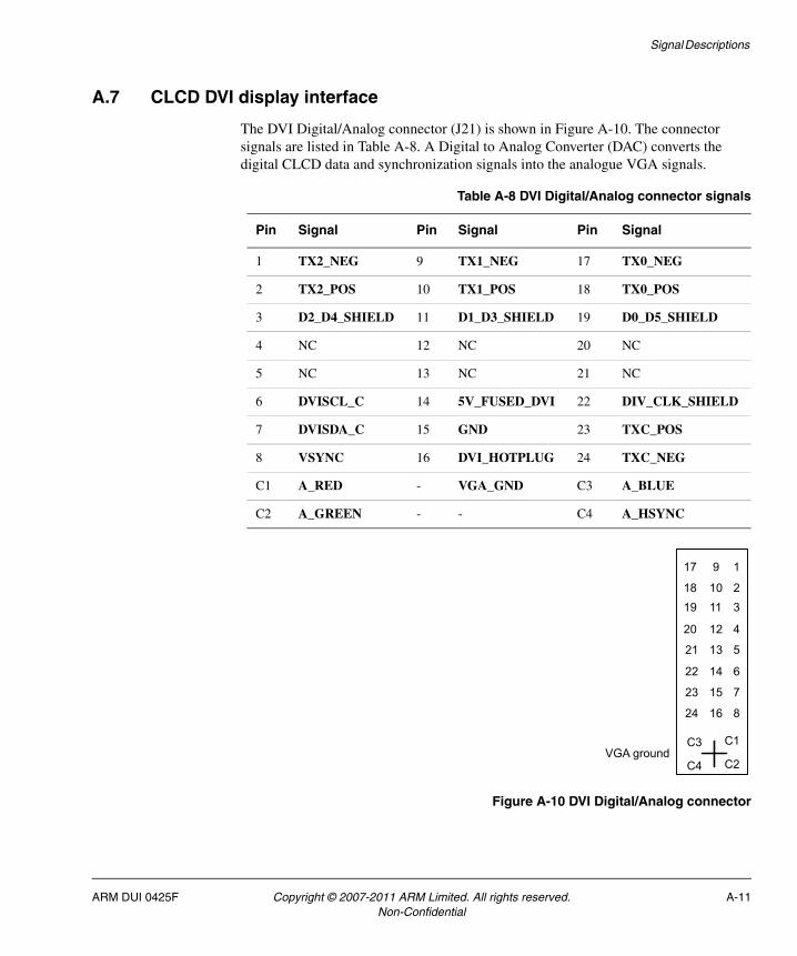
Signal Descriptions
A.7 CLCD DVI display interface
The DVI Digital/Analog connector (J21) is shown in Figure A-10. The connector signals are listed in Table A-8. A Digital to Analog Converter (DAC) converts the digital CLCD data and synchronization signals into the analogue VGA signals.
Figure A-10 DVI Digital/Analog connector
Table A-8 DVI Digital/Analog connector signals
Pin Signal Pin Signal Pin Signal
1 TX2_NEG 9 TX1_NEG 17 TX0_NEG
2 TX2_POS 10 TX1_POS 18 TX0_POS
3 D2_D4_SHIELD 11 D1_D3_SHIELD 19 D0_D5_SHIELD
4 NC 12 NC 20 NC
5 NC 13 NC 21 NC
6 DVISCL_C 14 5V_FUSED_DVI 22 DIV_CLK_SHIELD
7 DVISDA_C 15 GND 23 TXC_POS
8 VSYNC 16 DVI_HOTPLUG 24 TXC_NEG
C1 A_RED - VGA_GND C3 A_BLUE
C2 A_GREEN - - C4 A_HSYNC
5
1
23
4
6
7
8
13
9
1011
12
14
15
16
21
17
1819
20
22
23
24
C3
C4
C1
C2VGA ground
ARM DUI 0425F Copyright © 2007-2011 ARM Limited. All rights reserved. A-11Non-Confidential

Signal Descriptions
A.8 GPIO interface
One eight-bit General Purpose Input/Output (GPIO) controller is incorporated into the ARM1176JZF-S development chip and one is implemented in the FPGA. The signals on the GPIO connector are shown in Figure A-11.
Figure A-11 GPIO connector
Note Each data pin has an on-board 10KΩ pullup resistor to 3.3V.
3V3
GP0_0
GP0_1
GP0_2
GP0_3
GP0_4
GP0_5
GP0_6
GP0_7
3V3
GND
GND
GND
GND
GND
GND
GND
GND
GND
1
33
2
34
GND
GND
GND
GND
GND
GND
GND
GP1_0
GP1_1
GP1_2
GP1_3
GP1_4
GP1_5
GP1_6
GP1_7
A-12 Copyright © 2007-2011 ARM Limited. All rights reserved. ARM DUI 0425FNon-Confidential

Signal Descriptions
A.9 Keyboard and mouse interface
The pinout of the KMI connectors J35 and J36 is shown in Figure A-12.
Figure A-12 KMI connector
Table A-9 shows signals on the KMI connectors.
12
34
56
Table A-9 Mouse and keyboard port signal descriptions
PinKeyboard (KMI0, J36) Mouse (KMI1, J35)
Signal Function Signal Function
1 KDATA Keyboard data MDATA Mouse Data
2 NC Not connected NC Not connected
3 GND Ground GND Ground
4 5V Fused 5V 5V Fused 5V
5 KCLK Keyboard clock MCLK Mouse clock
6 NC Not connected NC Not connected
ARM DUI 0425F Copyright © 2007-2011 ARM Limited. All rights reserved. A-13Non-Confidential
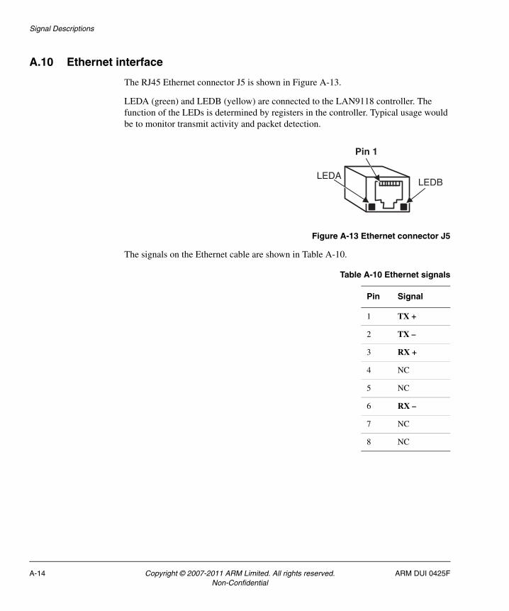
Signal Descriptions
A.10 Ethernet interface
The RJ45 Ethernet connector J5 is shown in Figure A-13.
LEDA (green) and LEDB (yellow) are connected to the LAN9118 controller. The function of the LEDs is determined by registers in the controller. Typical usage would be to monitor transmit activity and packet detection.
Figure A-13 Ethernet connector J5
The signals on the Ethernet cable are shown in Table A-10.
LEDB
Pin 1
LEDA
Table A-10 Ethernet signals
Pin Signal
1 TX +
2 TX –
3 RX +
4 NC
5 NC
6 RX –
7 NC
8 NC
A-14 Copyright © 2007-2011 ARM Limited. All rights reserved. ARM DUI 0425FNon-Confidential

Signal Descriptions
A.11 RealView Logic Tile header connectors
These headers enable the connection of a RealView Logic Tile to the PB1176JZF-S. Figure A-14 shows the pin numbers and power-blade usage of the HDRX, HDRY, and HDRZ headers. See Appendix C RealView Logic Tile for details of the RealView Logic Tile connectors.
Figure A-14 RealView Logic Tile HDRX, HDRY, and HDRZ pin numbering
ARM DUI 0425F Copyright © 2007-2011 ARM Limited. All rights reserved. A-15Non-Confidential
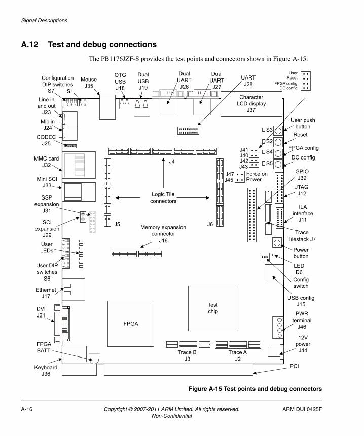
Signal Descriptions
A.12 Test and debug connections
The PB1176JZF-S provides the test points and connectors shown in Figure A-15.
Figure A-15 Test points and debug connectors
Testchip
FPGA
12
34
56
78
ConfigurationDIP switches
GPIOJ39
PWR terminal
J46
12V power
J44
DVIJ21
KeyboardJ36
MouseJ35
User DIP switches
S6
User LEDs
Line in and out
J23Mic inJ24
MMC cardJ32
Mini SCIJ33
Logic Tile connectors
Memory expansion connector
J16
EthernetJ17 USB config
J15
JTAGJ12
User push button
Power button
SSP expansion
J31
PCI
Trace BJ3
Trace AJ2
OTG USBJ18
Dual USBJ19
Dual UARTJ26
Dual UARTJ27
UARTJ28
CODECJ25
1 21 2 3 4
S7 S1Character
LCD displayJ37
Reset
DC config
ILA interface
J11
FPGA BATT
SCI expansion
J29
J4
J5 J6
S3
S2
S4
S5
FPGA config
Configswitch
J41J40J42J43
UserReset
FPGA config
J47J45
DC config
Force onPower
Trace Tilestack J7
LEDD6
A-16 Copyright © 2007-2011 ARM Limited. All rights reserved. ARM DUI 0425FNon-Confidential

Signal Descriptions
This section contains the following subsections:
• JTAG
• USB debug port
• Trace connector pinout on page A-18
• Integrated logic analyzer on page A-21.
A.12.1 JTAG
Figure A-16 shows the pinout of the JTAG connector J12 and Table 3-10 on page 3-55 provides a description of the JTAG and related signals. All JTAG active HIGH input signals have pull-up resistors (DGBRQ is active LOW and has a pull-down resistor).
Note The term JTAG equipment refers to any hardware that can drive the JTAG signals to devices in the scan chain. Typically this is RealView ICE, although hardware from other suppliers can also be used to debug ARM processors.
Figure A-16 JTAG connector J12
A.12.2 USB debug port
Figure A-17 on page A-18 shows the signals on the USB debug connector J15. USBDP and USBDM are the positive and negative USB data signals. The USB debug port can be used to load new images into the PB1176JZF-S FPGA or into FPGAs on attached Logic Tiles.
3V33V3GNDGNDGNDGNDGNDGNDGNDGNDGND
nTRSTTDI
TMSTCK
RTCKTDO
nSRSTDBGRQ
DBGACK
1
19
2
20
ARM DUI 0425F Copyright © 2007-2011 ARM Limited. All rights reserved. A-17Non-Confidential

Signal Descriptions
Figure A-17 USB debug connector J15
A.12.3 Trace connector pinout
The Mictor connector that is used for trace signals is shown in Figure A-18.
Figure A-18 AMP Mictor connector
Table A-11 and Table A-12 on page A-19 lists the pinouts of the development chip trace connectors.
2 USBDM
3 USBDP
VCC 1
GND 4
1
2
37
38
Table A-11 Trace connector J2
Channel Pin Pin Channel
5VDC 1 2 Not connected
GND 3 4 Not connected
GND 5 6 TRACECLK
NC 7 8 NC
NC 9 10 NC
NC 11 12 3V3
NC 13 14 3V3
NC 15 16 TRACEDATA7
NC 17 18 TRACEDATA6
NC 19 20 TRACEDATA5
A-18 Copyright © 2007-2011 ARM Limited. All rights reserved. ARM DUI 0425FNon-Confidential

Signal Descriptions
NC 21 22 TRACEDATA4
TRACEDATA15 23 24 TRACEDATA3
TRACEDATA14 25 26 TRACEDATA2
TRACEDATA13 27 28 TRACEDATA1
TRACEDATA12 29 30 GND
TRACEDATA11 31 32 GND
TRACEDATA10 33 34 3V3
TRACEDATA9 35 36 TRACECTL
TRACEDATA8 37 38 TRACEDATA0
Table A-12 Trace connector J3
Channel Pin Pin Channel
5VDC 1 2 Not connected
GND 3 4 Not connected
GND 5 6 TRACECLK
NC 7 8 NC
NC 9 10 NC
NC 11 12 3V3
NC 13 14 3V3
NC 15 16 TRACEDATA23
NC 17 18 TRACEDATA22
NC 19 20 TRACEDATA21
NC 21 22 TRACEDATA20
TRACEDATA31 23 24 TRACEDATA19
TRACEDATA30 25 26 TRACEDATA18
Table A-11 Trace connector J2 (continued)
Channel Pin Pin Channel
ARM DUI 0425F Copyright © 2007-2011 ARM Limited. All rights reserved. A-19Non-Confidential

Signal Descriptions
Table A-13 lists the pinouts of the Logic Tile trace connector J7. The Logic Tile trace connector is not restricted to use only as a trace connector. The connector can be used to monitor any signals that are implemented on the specified header pins.
TRACEDATA29 27 28 TRACEDATA17
TRACEDATA28 29 30 GND
TRACEDATA27 31 32 GND
TRACEDATA26 33 34 3V3
TRACEDATA25 35 36 GND
TRACEDATA24 37 38 TRACEDATA16
Table A-13 Logic Tile trace connector J7
Channel Pin Pin Channel
NC 1 2 Not connected
GND 3 4 Not connected
Y178 5 6 Y179
Y177 7 8 Y168
Y152 9 10 Y167
Y151 11 12 Y166
Y150 13 14 Y165
Y149 15 16 Y164
Y148 17 18 Y163
Y147 19 20 Y162
Y146 21 22 Y161
Y176 23 24 Y160
Y175 25 26 Y159
Y174 27 28 Y158
Table A-12 Trace connector J3 (continued)
Channel Pin Pin Channel
A-20 Copyright © 2007-2011 ARM Limited. All rights reserved. ARM DUI 0425FNon-Confidential

Signal Descriptions
A.12.4 Integrated logic analyzer
Figure A-19 shows the signals on the integrated logic analyzer connector J11. Use an embedded logic analyzer to debug FPGA designs and software at the same time. For more information, see the documentation supplied with your analyzer. (The ChipScope product is described on the Xilinx web site at www.xilinx.com.)
Figure A-19 Integrated logic analyzer connector J11
Y173 29 30 Y157
Y172 31 32 Y156
Y171 33 34 Y155
Y170 35 36 Y154
Y169 37 38 Y153
Table A-13 Logic Tile trace connector J7 (continued)
Channel Pin Pin Channel
8 ILA_TDO
SS
P c
onne
ctor
3
11
4 ILA_TMS
6 ILATCK
2 3V3
5
10 ILATDI
12 NC
14 NC
7
9
13
10K
ARM DUI 0425F Copyright © 2007-2011 ARM Limited. All rights reserved. A-21Non-Confidential

Signal Descriptions
A-22 Copyright © 2007-2011 ARM Limited. All rights reserved. ARM DUI 0425FNon-Confidential

Appendix B Specifications
This appendix contains the specification for the PB1176JZF-S. It contains the following sections:
• Electrical specification on page B-2
• Clock rate restrictions on page B-4
• Mechanical details on page B-5.
ARM DUI 0425F Copyright © 2007-2011 ARM Limited. All rights reserved. B-1Non-Confidential
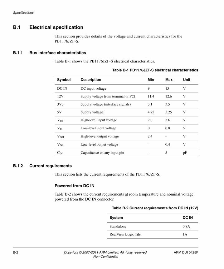
Specifications
B.1 Electrical specification
This section provides details of the voltage and current characteristics for the PB1176JZF-S.
B.1.1 Bus interface characteristics
Table B-1 shows the PB1176JZF-S electrical characteristics.
B.1.2 Current requirements
This section lists the current requirements of the PB1176JZF-S.
Powered from DC IN
Table B-2 shows the current requirements at room temperature and nominal voltage powered from the DC IN connector.
Table B-1 PB1176JZF-S electrical characteristics
Symbol Description Min Max Unit
DC IN DC input voltage 9 15 V
12V Supply voltage from terminal or PCI 11.4 12.6 V
3V3 Supply voltage (interface signals) 3.1 3.5 V
5V Supply voltage 4.75 5.25 V
VIH High-level input voltage 2.0 3.6 V
VIL Low-level input voltage 0 0.8 V
VOH High-level output voltage 2.4 - V
VOL Low-level output voltage - 0.4 V
CIN Capacitance on any input pin - 5 pF
Table B-2 Current requirements from DC IN (12V)
System DC IN
Standalone 0.8A
RealView Logic Tile 1A
B-2 Copyright © 2007-2011 ARM Limited. All rights reserved. ARM DUI 0425FNon-Confidential
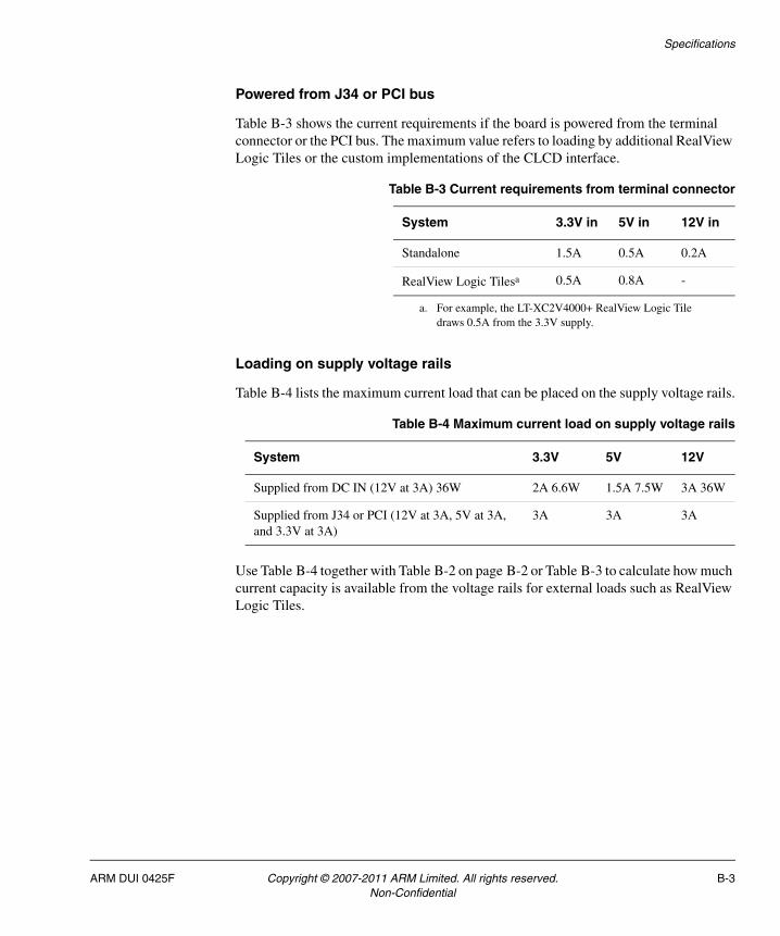
Specifications
Powered from J34 or PCI bus
Table B-3 shows the current requirements if the board is powered from the terminal connector or the PCI bus. The maximum value refers to loading by additional RealView Logic Tiles or the custom implementations of the CLCD interface.
Loading on supply voltage rails
Table B-4 lists the maximum current load that can be placed on the supply voltage rails.
Use Table B-4 together with Table B-2 on page B-2 or Table B-3 to calculate how much current capacity is available from the voltage rails for external loads such as RealView Logic Tiles.
Table B-3 Current requirements from terminal connector
System 3.3V in 5V in 12V in
Standalone 1.5A 0.5A 0.2A
RealView Logic Tilesa
a. For example, the LT-XC2V4000+ RealView Logic Tile draws 0.5A from the 3.3V supply.
0.5A 0.8A -
Table B-4 Maximum current load on supply voltage rails
System 3.3V 5V 12V
Supplied from DC IN (12V at 3A) 36W 2A 6.6W 1.5A 7.5W 3A 36W
Supplied from J34 or PCI (12V at 3A, 5V at 3A, and 3.3V at 3A)
3A 3A 3A
ARM DUI 0425F Copyright © 2007-2011 ARM Limited. All rights reserved. B-3Non-Confidential

Specifications
B.2 Clock rate restrictions
The default clock rates for reliable operation are:
CPU 210MHz
AXI/MDDR 105MHz
External AXI 35MHz
If you have added one or more RealView Logic Tiles, you might discover that you have to reduce these clock rates.
Caution The ICS307 programmable oscillators OSC0, OSC1, OSC2, OSC3, and OSC4 can be programmed to deliver very high clock signals (200MHZ). The only ARM1176JZF-S development chip clock input that can function at this frequency is PLLCLKEXT.
Also, the settings for VCO divider, output divider, and output select values are interrelated and must be set correctly. Some combinations of settings do not result in stable operation. For more information on the ICS clock generator and a frequency calculator, see the ICS web site at www.icst.com.
B-4 Copyright © 2007-2011 ARM Limited. All rights reserved. ARM DUI 0425FNon-Confidential
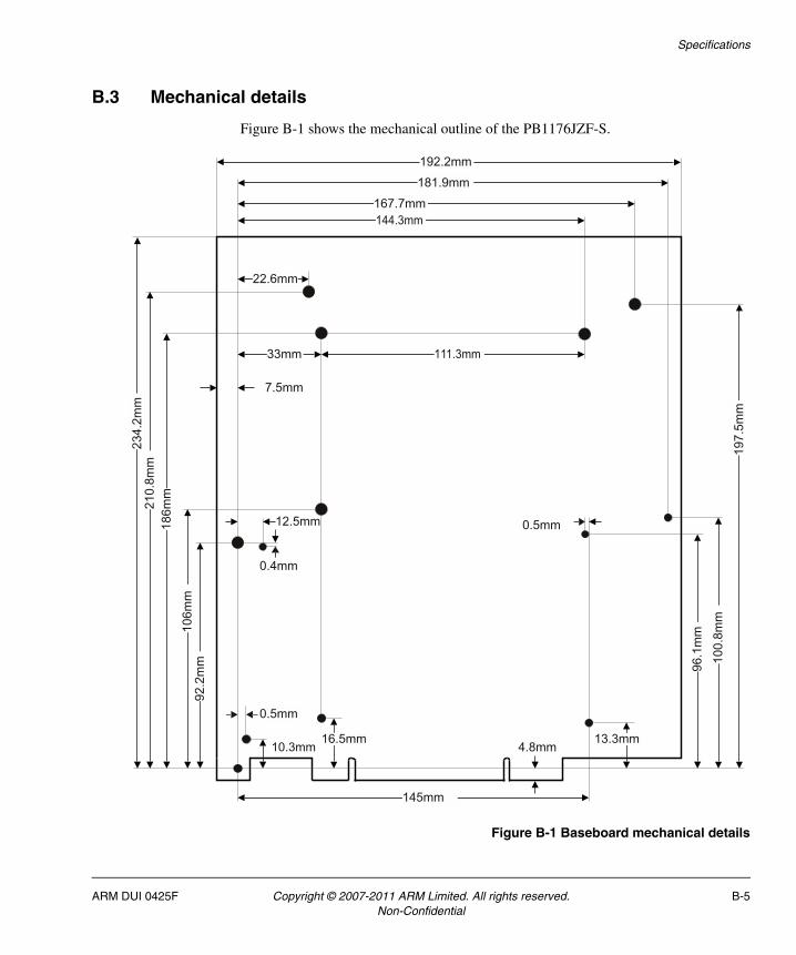
Specifications
B.3 Mechanical details
Figure B-1 shows the mechanical outline of the PB1176JZF-S.
Figure B-1 Baseboard mechanical details
0.5mm
7.5mm
10.3mm 4.8mm
0.4mm
12.5mm
234.
2mm
210.
8mm
186m
m
106m
m92
.2m
m
145mm
96.1
mm
100.
8mm
181.9mm
197.
5mm
167.7mm
192.2mm
22.6mm
111.3mm
13.3mm16.5mm
33mm
0.5mm
144.3mm
ARM DUI 0425F Copyright © 2007-2011 ARM Limited. All rights reserved. B-5Non-Confidential

Specifications
B-6 Copyright © 2007-2011 ARM Limited. All rights reserved. ARM DUI 0425FNon-Confidential

Appendix C RealView Logic Tile
This appendix describes the signals present on the RealView Logic Tile expansion headers. It contains the following sections:
• About the RealView Logic Tile on page C-2
• Signals on the tile header connectors on page C-7.
Note For more information on using the RealView Logic Tile, see the user guide for your tile.
ARM DUI 0425F Copyright © 2007-2011 ARM Limited. All rights reserved. C-1Non-Confidential
RealView Logic Tile
C.1 About the RealView Logic Tile
The ARM RealView Logic Tiles, for example the LT-XC2V6000 and LTXC4V160, enable developing AMBA AXI peripherals or custom logic.
Caution The PB1176JZF-S or attached RealView Logic Tile can be damaged by improper use:
• The PB1176JZF-S recommended limit is two.
When stacking tiles ensure that the power source can maintain the required voltage at the top tile when supplying maximum current to the system. If necessary, use a separate bench supply or power the system from a PCI backplane. See Current requirements from terminal connector on page B-3 for more details.
• The FPGA signals on a RealView Logic Tile and the PB1176JZF-S are fully programmable. Ensure that there are no clashes between the signals on the tiles or with the signals from the PB1176JZF-S.
The FPGA can be damaged if several pins configured as outputs are connected together and attempt to output different logic levels.
• The RealView Logic Tile mounted on the PB1176JZF-S must use the default 3.3V signal levels.
The following section describes:
• Variable I/O levels
• AXI buses on page C-3
• JTAG on page C-4.
C.1.1 Variable I/O levels
All HDRX, HDRY, and HDRZ connector signals on the PB1176JZF-S are fixed at 3.3V I/O signalling level.
The I/O voltage on a RealView Logic Tile (VCCO1 and VCC02) can be changed by removing resistors on the tile and supplying the I/O voltage from either the tile above or the tile below in a tile stack. However, all signals from the PB1176JZF-S to a RealView Logic Tile use 3.3V I/O levels and all signals from a RealView Logic Tile to the PB1176JZF-S must use 3.3V I/O levels.
The 5V supply on the headers is to power voltage converters that might be present on the Logic Tile.
C-2 Copyright © 2007-2011 ARM Limited. All rights reserved. ARM DUI 0425FNon-Confidential

RealView Logic Tile
C.1.2 AXI buses
The AXI master and slave data signals are multiplexed to reduce the number of pins used on the tile headers:
• The PB1176JZF-S development chip AXI master connects to HDR Y.
• The PB1176JZF-S FPGA AXI slave bus connects to HDR X.
Note If a Logic Tile is not fitted, the multiplexed PB1176JZF-S development chip
master connects directly to the FPGA slave by smart switches.
If a Logic Tile is fitted, the direct connection is disabled and an AXI master and slave interface must be implemented in the tile FPGA to pass accesses from the development chip to the PB1176JZF-S FPGA slave.
• The PB1176JZF-S development chip AXI sideband bus signals are connected to HDR Z.
Figure C-1 AXI busses on Logic Tile
Logic Tile
HD
RX
HDRZ
HD
RY
Demux
nTIL
ED
ET
ARM1176JZF-S development chipFPGA
AXI S AXI M
Mux
Sideband
ARM DUI 0425F Copyright © 2007-2011 ARM Limited. All rights reserved. C-3Non-Confidential

RealView Logic Tile
C.1.3 JTAG
The JTAG signals for the FPGA on the RealView Logic Tile are shown in Figure C-2. If a tile is connected to the baseboard, the nTILE_DET signal is grounded and the JTAG signals and AXI bus are routed through the tile.
There is not a JTAG connector on the RealView Logic Tile. Use the JTAG or USB debug connector on the baseboard to program the configuration flash in the RealView Logic Tile to directly load the RealView Logic Tile FPGA image.
The nCFGEN signal is controlled by the CONFIG jumper on the baseboard and selects debug or configuration mode for the tile FPGA and PLD. If the Logic Tile does not implement a debuggable core, the FPGA must interconnect the input and output D_ signals. For more information on JTAG signals and the difference between debug and configuration mode, see JTAG debug port and USB config port support on page 3-51.
Figure C-2 JTAG signals to Logic Tiles
FPGA
Logic Tile
Baseboard
C_T
DO
nSR
STC
_nSR
ST
D_n
SRST
C_n
TRST
nTR
ST
D_n
TRST
nCFG
EN
C_T
MS
nTIL
E_D
ET
D_T
DO
_OU
T
C_T
DI
D_T
DI
C_T
CK
_IN
C_T
CK
D_T
CK
D_T
DO
D_R
TCK
D_T
MS
PLD
ARM
C_T
DO
_OU
T
To A
XI b
us
switc
hes
Con
fig
Mode control
Reset signals
C-4 Copyright © 2007-2011 ARM Limited. All rights reserved. ARM DUI 0425FNon-Confidential

RealView Logic Tile
C.1.4 RealView Logic Tile clocks
Table C-1 lists the RealView Logic Tile clocks. See the user guide for your Logic Tile for more information on using clocks.
Each tile can receive or generate the shared CLK_GLOBAL signal depending on the state of the tile signal CLK_GLOBAL_EN:
• If LOW, the local tile signal CLK_GLOBAL_OUT is driven onto CLK_GLOBAL and to the CLK_GLOBAL_IN input of the FPGAs on the tile.
• If HIGH, the external CLK_GLOBAL signal goes to the CLK_GLOBAL_INinput of the FPGAs on the tile.
Note Some of the standard RealView Logic Tile clocks, CLK_NEG_DN_IN for example, are not used. Ensure that your RealView Logic Tile configuration is compatible with the clock sources you are using from the PB1176JZF-S.
Table C-1 RealView Logic Tile clock signals
Tile signal Direction Description
CLK_UP_THRU To tile From PB1176JZF-S AXI Master multiplexor logic
CLK_OUT_PLUS1 To tile From PB1176JZF-S AXI Slave multiplexor to RealView Logic Tile.
CLK_OUT_PLUS2 To tile From PB1176JZF-S AXI Slave multiplexor to RealView Logic Tile.
CLK_GLOBAL I/O Global clock connected to all RealView Logic Tiles (reserved for future use).
CLK_NEG_DN_IN From tile To PB1176JZF-S FPGA (reserved for future use).
CLK_POS_DN_IN From tile To PB1176JZF-S FPGA (reserved for future use).
CLK_NEG_UP_OUT To tile FPGA clock to RealView Logic Tile (reserved for future use).
CLK_POS_UP_OUT To tile development chip clock to RealView Logic Tile (reserved for future use).
CLK_IN_PLUS1 From tile To PB1176JZF-S FPGA (reserved for future use).
CLK_IN_PLUS2 From tile To PB1176JZF-S FPGA (reserved for future use).
CLK_DN_THRU - Not connected
ARM DUI 0425F Copyright © 2007-2011 ARM Limited. All rights reserved. C-5Non-Confidential

RealView Logic Tile
C.1.5 Reset signals
Table C-2 describes reset signals.
Reset timing
Figure C-3 shows the power-on reset sequence.
Figure C-3 Power-on reset and configuration timing
Table C-2 Reset signal descriptions
Name Function
nBOARDPOR This signal is generated on the baseboard and initiates the configuration of the baseboard FPGA, development chip, and PLDs.
This signal is also used to generate the JTAG reset signals at power on.
Logic Tile LOCAL_DONE
This signal is generated on the Logic Tile and indicates that FPGA on the Logic Tile has been configured.
GLOBAL_DONE This is an open-collector configuration signal that goes HIGH when the baseboard and all attached Logic Tiles have finished configuring and released their LOCAL_DONE signal. The system is held in reset until this signal goes HIGH. The length of time GLOBAL_DONE is LOW depends on the system configuration.
nSYSPOR Power-on reset signal from the baseboard that initializes the reset level state machine after GLOBAL_DONE goes HIGH.
Shared GLOBAL_DONE signal
Baseboard nSYSPOR
Logic Tile LOCAL_DONE
Baseboard local reset signal nBOARDPOR
Baseboard JTAG reset signals
7μs
Released by baseboard and other Logic Tiles2.6μs
Baseboard power supply voltage
200ms
C-6 Copyright © 2007-2011 ARM Limited. All rights reserved. ARM DUI 0425FNon-Confidential

RealView Logic Tile
C.2 Signals on the tile header connectors
This section gives an detailed listing of the RealView Logic Tile header connectors on the PB1176JZF-S.
There are three headers on the top and bottom of the tile. The HDRX and HDRY headers are 180-way and the HDRZ connectors are 300-way.
Figure C-4 shows the pin numbers and power-blade usage of the HDRX, HDRY, and HDRZ headers on the PB1176JZF-S tile headers. See RealView Logic Tile header connectors on page A-15 for details of the signals on the PB1176JZF-S header connectors.
Figure C-4 HDRX, HDRY, and HDRZ pin numbering
The following section describes:
• HDRX signals
• HDRY signals on page C-14
• HDRZ on page C-20.
C.2.1 HDRX signals
Table C-3 on page C-8 describes the signals on the HDRX header pins. For a description of the signals see the AMBA 3 AXI Protocol (ARM IHI 0022).i
ARM DUI 0425F Copyright © 2007-2011 ARM Limited. All rights reserved. C-7Non-Confidential
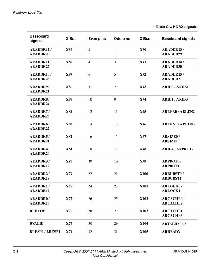
RealView Logic Tile
Table C-3 HDRX signals
Baseboard signals
X Bus Even pins Odd pins X Bus Baseboard signals
ARADDR12 / ARADDR28
X89 2 1 X90 ARADDR13 / ARADDR29
ARADDR11 / ARADDR27
X88 4 3 X91 ARADDR14 / ARADDR30
ARADDR10 / ARADDR26
X87 6 5 X92 ARADDR15 / ARADDR31
ARADDR9 / ARADDR25
X86 8 7 X93 ARID0 / ARID2
ARADDR8 / ARADDR24
X85 10 9 X94 ARID1 / ARID3
ARADDR7 / ARADDR23
X84 12 11 X95 ARLEN0 / ARLEN2
ARADDR6 / ARADDR22
X83 14 13 X96 ARLEN1 / ARLEN3
ARADDR5 / ARADDR21
X82 16 15 X97 ARSIZE0 / ARSIZE1
ARADDR4 / ARADDR20
X81 18 17 X98 ARID4 / ARPROT2
ARADDR3 / ARADDR19
X80 20 19 X99 ARPROT0 / ARPROT1
ARADDR2 / ARADDR18
X79 22 21 X100 ARBURST0 / ARBURST1
ARADDR1 / ARADDR17
X78 24 23 X101 ARLOCK0 / ARLOCK1
ARADDR0 / ARADDR16
X77 26 25 X102 ARCACHE0 / ARCACHE2
BREADY X76 28 27 X103 ARCACHE1 / ARCACHE3
BVALID X75 30 29 X104 ARVALID / b0a
BRESP0 / BRESP1 X74 32 31 X105 ARREADY
C-8 Copyright © 2007-2011 ARM Limited. All rights reserved. ARM DUI 0425FNon-Confidential

RealView Logic Tile
BID4 / (not connected)
X73 34 33 X106 RDATA0 / RDATA32
BID1 / BID3 X72 36 35 X107 RDATA1 / RDATA33
BID0 / BID2 X71 38 37 X108 RDATA2 / RDATA34
AWREADY X70 40 39 X109 RDATA3 / RDATA35
AWVALID / b0b X69 42 41 X110 RDATA4 / RDATA36
AWCACHE1 / AWCACHE3
X68 44 43 X111 RDATA5 / RDATA37
AWCACHE0 / AWCACHE2
X67 46 45 X112 RDATA6 / RDATA38
AWLOCK0 / AWLOCK1
X66 48 47 X113 RDATA7 / RDATA39
AWBURST0 / AWBURST1
X65 50 49 X114 RDATA8 / RDATA40
AWPROT0 / AWPROT1
X64 52 51 X115 RDATA9 / RDATA41
ARM_nRESET (not connected)
X63 54 53 X116 RDATA10 / RDATA42
AWID4 / AWPROT2
X62 56 55 X117 RDATA11 / RDATA43
AWSIZE0 / AWSIZE1
X61 58 57 X118 RDATA12 / RDATA44
AWLEN1 / AWLEN3
X60 60 59 X119 RDATA13 / RDATA45
AWLEN0 / AWLEN2
X59 62 61 X120 RDATA14 / RDATA46
Table C-3 HDRX signals (continued)
Baseboard signals
X Bus Even pins Odd pins X Bus Baseboard signals
ARM DUI 0425F Copyright © 2007-2011 ARM Limited. All rights reserved. C-9Non-Confidential
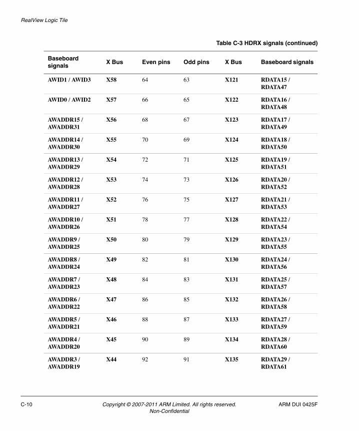
RealView Logic Tile
AWID1 / AWID3 X58 64 63 X121 RDATA15 / RDATA47
AWID0 / AWID2 X57 66 65 X122 RDATA16 / RDATA48
AWADDR15 / AWADDR31
X56 68 67 X123 RDATA17 / RDATA49
AWADDR14 / AWADDR30
X55 70 69 X124 RDATA18 / RDATA50
AWADDR13 / AWADDR29
X54 72 71 X125 RDATA19 / RDATA51
AWADDR12 / AWADDR28
X53 74 73 X126 RDATA20 / RDATA52
AWADDR11 / AWADDR27
X52 76 75 X127 RDATA21 / RDATA53
AWADDR10 / AWADDR26
X51 78 77 X128 RDATA22 / RDATA54
AWADDR9 / AWADDR25
X50 80 79 X129 RDATA23 / RDATA55
AWADDR8 / AWADDR24
X49 82 81 X130 RDATA24 / RDATA56
AWADDR7 / AWADDR23
X48 84 83 X131 RDATA25 / RDATA57
AWADDR6 / AWADDR22
X47 86 85 X132 RDATA26 / RDATA58
AWADDR5 / AWADDR21
X46 88 87 X133 RDATA27 / RDATA59
AWADDR4 / AWADDR20
X45 90 89 X134 RDATA28 / RDATA60
AWADDR3 / AWADDR19
X44 92 91 X135 RDATA29 / RDATA61
Table C-3 HDRX signals (continued)
Baseboard signals
X Bus Even pins Odd pins X Bus Baseboard signals
C-10 Copyright © 2007-2011 ARM Limited. All rights reserved. ARM DUI 0425FNon-Confidential

RealView Logic Tile
AWADDR2 / AWADDR18
X43 94 93 X136 RDATA30 / RDATA62
AWADDR1 / AWADDR17
X42 96 95 X137 RDATA31 / RDATA63
AWADDR0 / AWADDR16
X41 98 97 X138 RID0 / RID2
WREADY X40 100 99 X139 RID1 / RID3
WVALID / b0c X39 102 101 X140 RRESP0 / RRESP1
WLAST / WID4 X38 104 103 X141 RLAST / RID4
WSTRB3 / WSTRB7
X37 106 105 X142 RVALID / (not connected)
WSTRB2 / WSTRB6
X36 108 107 X143 RREADY
WSTRB1 / WSTRB5
X35 110 109 X144 X144
WSTRB0 / WSTRB4
X34 112 111 X145 X145
WID1 / WID3 X33 114 113 X146 X146
WID0 / WID2 X32 116 115 X147 X147
WDATA31 / WDATA63
X31 118 117 X148 X148
WDATA30 / WDATA62
X30 120 119 X149 X149
WDATA29 / WDATA61
X29 122 121 X150 X150
WDATA28 / WDATA60
X28 124 123 X151 X151
WDATA27 / WDATA59
X27 126 125 X152 X152
Table C-3 HDRX signals (continued)
Baseboard signals
X Bus Even pins Odd pins X Bus Baseboard signals
ARM DUI 0425F Copyright © 2007-2011 ARM Limited. All rights reserved. C-11Non-Confidential

RealView Logic Tile
WDATA26 / WDATA58
X26 128 127 X153 X153
WDATA25 / WDATA57
X25 130 129 X154 X154
WDATA24 / WDATA56
X24 132 131 X155 X155
WDATA23 / WDATA55
X23 134 133 X156 X156
WDATA22 / WDATA54
X22 136 135 X157 X157
WDATA21 / WDATA53
X21 138 137 X158 X158
WDATA20 / WDATA52
X20 140 139 X159 X159
WDATA19 / WDATA51
X19 142 141 X160 X160
WDATA18 / WDATA50
X18 144 143 X161 X161
WDATA17 / WDATA49
X17 146 145 X162 X162
WDATA16 / WDATA48
X16 148 147 X163 X163
WDATA15 / WDATA47
X15 150 149 X164 X164
WDATA14 / WDATA46
X14 152 151 X165 X165
WDATA13 / WDATA45
X13 154 153 X166 X166
WDATA12 / WDATA44
X12 156 155 X167 X167
Table C-3 HDRX signals (continued)
Baseboard signals
X Bus Even pins Odd pins X Bus Baseboard signals
C-12 Copyright © 2007-2011 ARM Limited. All rights reserved. ARM DUI 0425FNon-Confidential

RealView Logic Tile
WDATA11 / WDATA43
X11 158 157 X168 X168
WDATA10 / WDATA42
X10 160 159 X169 X169
WDATA9 / WDATA41
X9 162 161 X170 X170
WDATA8 / WDATA40
X8 164 163 X171 X171
WDATA7 / WDATA39
X7 166 165 X172 X172
WDATA6 / WDATA38
X6 168 167 X173 X173
WDATA5 / WDATA37
X5 170 169 X174 X174
WDATA4 / WDATA36
X4 172 171 X175 X175
WDATA3 / WDATA35
X3 174 173 X176 X176
WDATA2 / WDATA34
X2 176 175 X177 X177
WDATA1 / WDATA33
X1 178 177 X178 X178
WDATA0 / WDATA32
X0 180 179 X179 X179
a. These are AXI ARVALID/ARID5 signals. b0 indicates that for the ARID5 phase of the controlling clock signal, ARID5 is always set to logic level zero.
b. These are AXI AWVALID/AWID5 signals. b0 indicates that for the AWID5 phase of the controlling clock signal, AWID5 is always set to logic level zero.
c. These are AXI WVALID/WID5 signals. b0 indicates that for the WID5 phase of the controlling clock signal, WID5 is always set to logic level zero.
Table C-3 HDRX signals (continued)
Baseboard signals
X Bus Even pins Odd pins X Bus Baseboard signals
ARM DUI 0425F Copyright © 2007-2011 ARM Limited. All rights reserved. C-13Non-Confidential
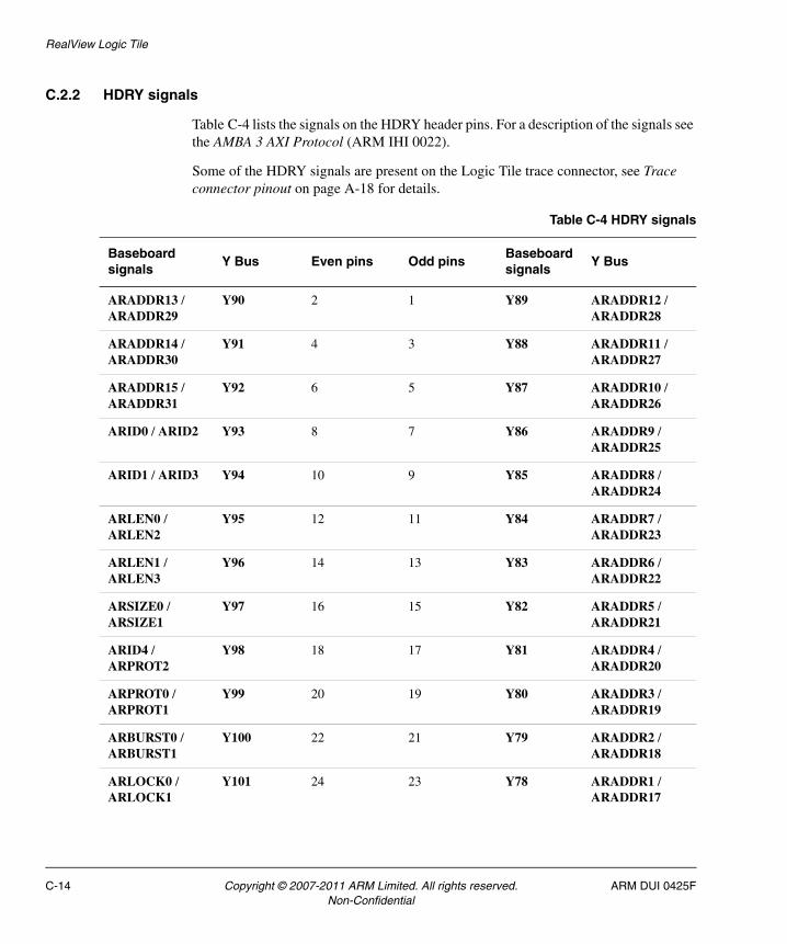
RealView Logic Tile
C.2.2 HDRY signals
Table C-4 lists the signals on the HDRY header pins. For a description of the signals see the AMBA 3 AXI Protocol (ARM IHI 0022).
Some of the HDRY signals are present on the Logic Tile trace connector, see Trace connector pinout on page A-18 for details.
Table C-4 HDRY signals
Baseboard signals
Y Bus Even pins Odd pinsBaseboard signals
Y Bus
ARADDR13 / ARADDR29
Y90 2 1 Y89 ARADDR12 / ARADDR28
ARADDR14 / ARADDR30
Y91 4 3 Y88 ARADDR11 / ARADDR27
ARADDR15 / ARADDR31
Y92 6 5 Y87 ARADDR10 / ARADDR26
ARID0 / ARID2 Y93 8 7 Y86 ARADDR9 / ARADDR25
ARID1 / ARID3 Y94 10 9 Y85 ARADDR8 / ARADDR24
ARLEN0 / ARLEN2
Y95 12 11 Y84 ARADDR7 / ARADDR23
ARLEN1 / ARLEN3
Y96 14 13 Y83 ARADDR6 / ARADDR22
ARSIZE0 / ARSIZE1
Y97 16 15 Y82 ARADDR5 / ARADDR21
ARID4 / ARPROT2
Y98 18 17 Y81 ARADDR4 / ARADDR20
ARPROT0 / ARPROT1
Y99 20 19 Y80 ARADDR3 / ARADDR19
ARBURST0 / ARBURST1
Y100 22 21 Y79 ARADDR2 / ARADDR18
ARLOCK0 / ARLOCK1
Y101 24 23 Y78 ARADDR1 / ARADDR17
C-14 Copyright © 2007-2011 ARM Limited. All rights reserved. ARM DUI 0425FNon-Confidential
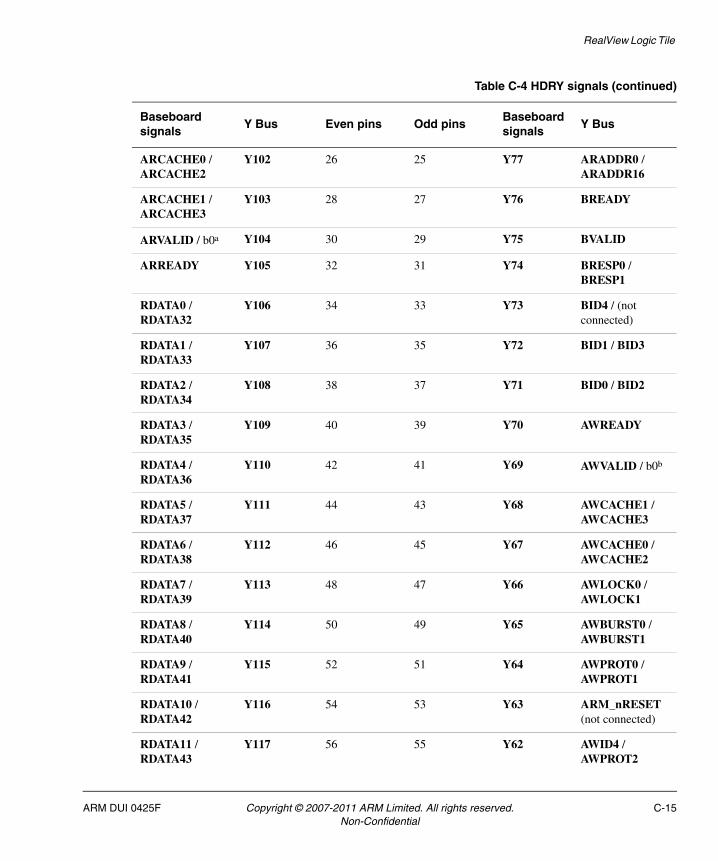
RealView Logic Tile
ARCACHE0 / ARCACHE2
Y102 26 25 Y77 ARADDR0 / ARADDR16
ARCACHE1 / ARCACHE3
Y103 28 27 Y76 BREADY
ARVALID / b0a Y104 30 29 Y75 BVALID
ARREADY Y105 32 31 Y74 BRESP0 / BRESP1
RDATA0 / RDATA32
Y106 34 33 Y73 BID4 / (not connected)
RDATA1 / RDATA33
Y107 36 35 Y72 BID1 / BID3
RDATA2 / RDATA34
Y108 38 37 Y71 BID0 / BID2
RDATA3 / RDATA35
Y109 40 39 Y70 AWREADY
RDATA4 / RDATA36
Y110 42 41 Y69 AWVALID / b0b
RDATA5 / RDATA37
Y111 44 43 Y68 AWCACHE1 / AWCACHE3
RDATA6 / RDATA38
Y112 46 45 Y67 AWCACHE0 / AWCACHE2
RDATA7 / RDATA39
Y113 48 47 Y66 AWLOCK0 / AWLOCK1
RDATA8 / RDATA40
Y114 50 49 Y65 AWBURST0 / AWBURST1
RDATA9 / RDATA41
Y115 52 51 Y64 AWPROT0 / AWPROT1
RDATA10 / RDATA42
Y116 54 53 Y63 ARM_nRESET (not connected)
RDATA11 / RDATA43
Y117 56 55 Y62 AWID4 / AWPROT2
Table C-4 HDRY signals (continued)
Baseboard signals
Y Bus Even pins Odd pinsBaseboard signals
Y Bus
ARM DUI 0425F Copyright © 2007-2011 ARM Limited. All rights reserved. C-15Non-Confidential
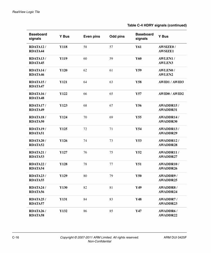
RealView Logic Tile
RDATA12 / RDATA44
Y118 58 57 Y61 AWSIZE0 / AWSIZE1
RDATA13 / RDATA45
Y119 60 59 Y60 AWLEN1 / AWLEN3
RDATA14 / RDATA46
Y120 62 61 Y59 AWLEN0 / AWLEN2
RDATA15 / RDATA47
Y121 64 63 Y58 AWID1 / AWID3
RDATA16 / RDATA48
Y122 66 65 Y57 AWID0 / AWID2
RDATA17 / RDATA49
Y123 68 67 Y56 AWADDR15 / AWADDR31
RDATA18 / RDATA50
Y124 70 69 Y55 AWADDR14 / AWADDR30
RDATA19 / RDATA51
Y125 72 71 Y54 AWADDR13 / AWADDR29
RDATA20 / RDATA52
Y126 74 73 Y53 AWADDR12 / AWADDR28
RDATA21 / RDATA53
Y127 76 75 Y52 AWADDR11 / AWADDR27
RDATA22 / RDATA54
Y128 78 77 Y51 AWADDR10 / AWADDR26
RDATA23 / RDATA55
Y129 80 79 Y50 AWADDR9 / AWADDR25
RDATA24 / RDATA56
Y130 82 81 Y49 AWADDR8 / AWADDR24
RDATA25 / RDATA57
Y131 84 83 Y48 AWADDR7 / AWADDR23
RDATA26 / RDATA58
Y132 86 85 Y47 AWADDR6 / AWADDR22
Table C-4 HDRY signals (continued)
Baseboard signals
Y Bus Even pins Odd pinsBaseboard signals
Y Bus
C-16 Copyright © 2007-2011 ARM Limited. All rights reserved. ARM DUI 0425FNon-Confidential

RealView Logic Tile
RDATA27 / RDATA59
Y133 88 87 Y46 AWADDR5 / AWADDR21
RDATA28 / RDATA60
Y134 90 89 Y45 AWADDR4 / AWADDR20
RDATA29 / RDATA61
Y135 92 91 Y44 AWADDR3 / AWADDR19
RDATA30 / RDATA62
Y136 94 93 Y43 AWADDR2 / AWADDR18
RDATA31 / RDATA63
Y137 96 95 Y42 AWADDR1 / AWADDR17
RID0 / RID2 Y138 98 97 Y41 AWADDR0 / AWADDR16
RID1 / RID3 Y139 100 99 Y40 WREADY
RRESP0 / RRESP1
Y140 102 101 Y39 WVALID / b0c
RLAST / RID4 Y141 104 103 Y38 WLAST / WID4
RVALID / (not connected)
Y142 106 105 Y37 WSTRB3 / WSTRB7
RREADY Y143 108 107 Y36 WSTRB2 / WSTRB6
Y144 Y144 110 109 Y35 WSTRB1 / WSTRB5
Y145 Y145 112 111 Y34 WSTRB0 / WSTRB4
Y146 Y146 114 113 Y33 WID1 / WID3
Y147 Y147 116 115 Y32 WID0 / WID2
Y148 Y148 118 117 Y31 WDATA31 / WDATA63
Y149 Y149 120 119 Y30 WDATA30 / WDATA62
Table C-4 HDRY signals (continued)
Baseboard signals
Y Bus Even pins Odd pinsBaseboard signals
Y Bus
ARM DUI 0425F Copyright © 2007-2011 ARM Limited. All rights reserved. C-17Non-Confidential

RealView Logic Tile
Y150 Y150 122 121 Y29 WDATA29 / WDATA61
Y151 Y151 124 123 Y28 WDATA28 / WDATA60
Y152 Y152 126 125 Y27 WDATA27 / WDATA59
Y153 Y153 128 127 Y26 WDATA26 / WDATA58
Y154 Y154 130 129 Y25 WDATA25 / WDATA57
Y155 Y155 132 131 Y24 WDATA24 / WDATA56
Y156 Y156 134 133 Y23 WDATA23 / WDATA55
Y157 Y157 136 135 Y22 WDATA22 / WDATA54
Y158 Y158 138 137 Y21 WDATA21 / WDATA53
Y159 Y159 140 139 Y20 WDATA20 / WDATA52
Y160 Y160 142 141 Y19 WDATA19 / WDATA51
Y161 Y161 144 143 Y18 WDATA18 / WDATA50
Y162 Y162 146 145 Y17 WDATA17 / WDATA49
Y163 Y163 148 147 Y16 WDATA16 / WDATA48
Y164 Y164 150 149 Y15 WDATA15 / WDATA47
Table C-4 HDRY signals (continued)
Baseboard signals
Y Bus Even pins Odd pinsBaseboard signals
Y Bus
C-18 Copyright © 2007-2011 ARM Limited. All rights reserved. ARM DUI 0425FNon-Confidential

RealView Logic Tile
Y165 Y165 152 151 Y14 WDATA14 / WDATA46
Y166 Y166 154 153 Y13 WDATA13 / WDATA45
Y167 Y167 156 155 Y12 WDATA12 / WDATA44
Y168 Y168 158 157 Y11 WDATA11 / WDATA43
Y169 Y169 160 159 Y10 WDATA10 / WDATA42
Y160 Y170 162 161 Y9 WDATA9 / WDATA41
Y171 Y171 164 163 Y8 WDATA8 / WDATA40
Y172 Y172 166 165 Y7 WDATA7 / WDATA39
Y173 Y173 168 167 Y6 WDATA6 / WDATA38
Y174 Y174 170 169 Y5 WDATA5 / WDATA37
Y175 Y175 172 171 Y4 WDATA4 / WDATA36
Y176 Y176 174 173 Y3 WDATA3 / WDATA35
Y177 Y177 176 175 Y2 WDATA2 / WDATA34
Y178 Y178 178 177 Y1 WDATA1 / WDATA33
Y179 Y179 180 179 Y0 WDATA0 / WDATA32
Table C-4 HDRY signals (continued)
Baseboard signals
Y Bus Even pins Odd pinsBaseboard signals
Y Bus
ARM DUI 0425F Copyright © 2007-2011 ARM Limited. All rights reserved. C-19Non-Confidential

RealView Logic Tile
C.2.3 HDRZ
Table C-5 lists the signals on the HDRZ header pins. See the user guide for the fitted Logic Tile for the tile-specific HDRZ upper (U) and HDRZ lower (L) signal listing.
Signals on HDRZ that are not connected to the baseboard are indicated by NC in Table C-5 (for example Z[255:224]).
Signals Z[233:199] are connected to the FPGA and are reserved for future expansion and must not be driven by the Logic Tile.)
Signals Z[198:128] are connected to the ARM1176JZF-S development chip. (Z[128:172] are test signal outputs and must not be driven by the Logic Tile. Z[198:173] are interrupt inputs.)
a. These are AXI ARVALID/ARID5 signals. b0 indicates that for the ARID5 phase of the controlling clock signal, ARID5 it is always set to logic level zero.
b. These are AXI AWVALID/AWID5 signals. b0 indicates that for the AWID5 phase of the controlling clock signal, AWID5 it is always set to logic level zero.
c. These are AXI WVALID/WID5 signals. b0 indicates that for the WID5 phase of the controlling clock signal, WID5 it is always set to logic level zero.
Table C-5 HDRZ signals
Baseboard signalsEven pins
Odd pins
Baseboard signals
NC (Z255) 2 1 Reserved (Z128)
NC (Z254) 4 3 Reserved (Z129)
NC (Z253) 6 5 Reserved (Z130)
NC (Z252) 8 7 Reserved (Z131)
NC (Z251) 10 9 Reserved (Z132)
NC (Z250) 12 11 Reserved (Z133)
NC (Z249) 14 13 Reserved (Z134)
NC (Z248) 16 15 Reserved (Z135)
NC (Z247) 18 17 Reserved (Z136)
NC (Z246) 20 19 Reserved (Z137)
NC (Z245) 22 21 Reserved (Z138)
NC (Z244) 24 23 Reserved (Z139)
C-20 Copyright © 2007-2011 ARM Limited. All rights reserved. ARM DUI 0425FNon-Confidential
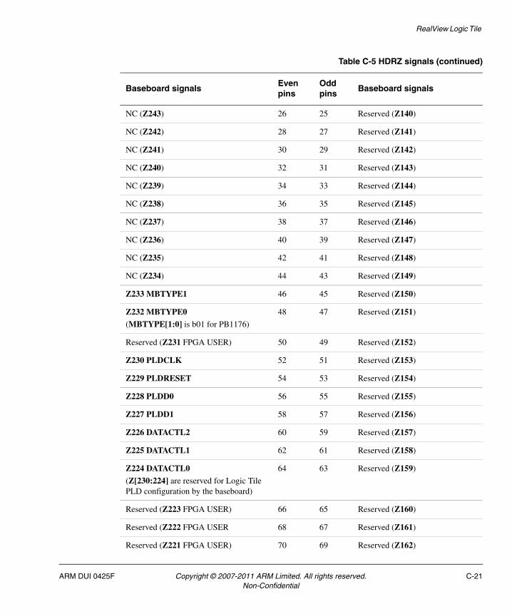
RealView Logic Tile
NC (Z243) 26 25 Reserved (Z140)
NC (Z242) 28 27 Reserved (Z141)
NC (Z241) 30 29 Reserved (Z142)
NC (Z240) 32 31 Reserved (Z143)
NC (Z239) 34 33 Reserved (Z144)
NC (Z238) 36 35 Reserved (Z145)
NC (Z237) 38 37 Reserved (Z146)
NC (Z236) 40 39 Reserved (Z147)
NC (Z235) 42 41 Reserved (Z148)
NC (Z234) 44 43 Reserved (Z149)
Z233 MBTYPE1 46 45 Reserved (Z150)
Z232 MBTYPE0
(MBTYPE[1:0] is b01 for PB1176)
48 47 Reserved (Z151)
Reserved (Z231 FPGA USER) 50 49 Reserved (Z152)
Z230 PLDCLK 52 51 Reserved (Z153)
Z229 PLDRESET 54 53 Reserved (Z154)
Z228 PLDD0 56 55 Reserved (Z155)
Z227 PLDD1 58 57 Reserved (Z156)
Z226 DATACTL2 60 59 Reserved (Z157)
Z225 DATACTL1 62 61 Reserved (Z158)
Z224 DATACTL0
(Z[230:224] are reserved for Logic Tile PLD configuration by the baseboard)
64 63 Reserved (Z159)
Reserved (Z223 FPGA USER) 66 65 Reserved (Z160)
Reserved (Z222 FPGA USER 68 67 Reserved (Z161)
Reserved (Z221 FPGA USER) 70 69 Reserved (Z162)
Table C-5 HDRZ signals (continued)
Baseboard signalsEven pins
Odd pins
Baseboard signals
ARM DUI 0425F Copyright © 2007-2011 ARM Limited. All rights reserved. C-21Non-Confidential

RealView Logic Tile
Reserved (Z220 FPGA USER) 72 71 Reserved (Z163)
Reserved (Z219 FPGA USER) 74 73 Reserved (Z164)
Reserved (Z218 FPGA USER) 76 75 Reserved (Z165)
Reserved (Z217 FPGA USER) 78 77 Reserved (Z166)
Reserved (Z216 FPGA USER) 80 79 Reserved (Z167)
Reserved (Z215 FPGA USER) 82 81 Reserved (Z168)
Reserved (Z214 FPGA USER) 84 83 Reserved (Z169)
Reserved (Z213 FPGA USER) 86 85 Reserved (Z170)
Reserved (Z212 FPGA USER) 88 87 Reserved (Z171)
Reserved (Z211 FPGA USER) 90 89 Reserved (Z172)
Reserved (Z210 FPGA USER) 92 91 Z173 INTSOURCE0
Reserved (Z209 FPGA USER) 94 93 Z174 INTSOURCE1
Reserved (Z208 FPGA USER) 96 95 Z175 INTSOURCE2
Reserved (Z207 FPGA USER) 98 97 Z176 INTSOURCE3
Reserved (Z206 FPGA USER) 100 99 Z177 INTSOURCE4
Reserved (Z205 FPGA USER) 102 101 Z178 INTSOURCE5
Reserved (Z204 FPGA USER) 104 103 Z179 INTSOURCE6
Reserved (Z203 FPGA USER) 106 105 Z180 INTSOURCE7
Reserved (Z202 FPGA USER) 108 107 Z181 INTSOURCE8
Reserved (Z201 FPGA USER) 110 109 Z182 INTSOURCE9
Reserved (Z200 FPGA USER) 112 111 Z183 INTSOURCE10
Reserved (Z199 FPGA USER) 114 113 Z184 INTSOURCE11
Z198 EXTINTSOURCE3 116 115 Z185 INTSOURCE12
Z197 EXTINTSOURCE2 118 117 Z186 INTSOURCE13
Table C-5 HDRZ signals (continued)
Baseboard signalsEven pins
Odd pins
Baseboard signals
C-22 Copyright © 2007-2011 ARM Limited. All rights reserved. ARM DUI 0425FNon-Confidential

RealView Logic Tile
Z196 EXTINTSOURCE1 120 119 Z187 INTSOURCE14
Z195 EXTINTSOURCE0 122 121 Z188 INTSOURCE15
Z194 INTSOURCE21 124 123 Z189 INTSOURCE16
Z193 INTSOURCE20 126 125 Z190 INTSOURCE17
Z192 INTSOURCE19 128 127 Z191 INTSOURCE18
CLK_POS_DN_IN 130 129 nSRST
CLK_NEG_DN_IN 132 131 D_nTRST
CLK_POS_UP_OUT 134 133 D_TDO_IN
CLK_NEG_UP 136 135 D_TDI
GND (CLK_UP_THRU) 138 137 D_TCK_OUT
CLK_OUT_PLUS1 140 139 D_TMS_OUT
CLK_OUT_PLUS2 142 141 D_RTCK
CLK_IN_PLUS2 144 143 C_nSRST
CLK_IN_PLUS1 146 145 C_nTRST
Z182 (CLK_DN_THRU) 148 147 C_TDO_IN
CLK_GLOBAL 150 149 C_TDI
FPGA_IMAGE 152 151 C_TCK_OUT
nSYSPOR 154 153 C_TMS_OUT
nSYSRST 156 155 nTILE_DET
NC (nRTCKEN) 158 157 nCFGEN
NC (SPARE12 reserved) 160 159 GLOBAL_DONE
NC (SPARE10 reserved) 162 161 NC (SPARE11 reserved)
NC (SPARE8 reserved) 164 163 NC (SPARE9 reserved)
NC (SPARE6 reserved) 166 165 NC (SPARE7 reserved)
Table C-5 HDRZ signals (continued)
Baseboard signalsEven pins
Odd pins
Baseboard signals
ARM DUI 0425F Copyright © 2007-2011 ARM Limited. All rights reserved. C-23Non-Confidential

RealView Logic Tile
NC (SPARE4 reserved) 168 167 NC (SPARE5 reserved)
NC (SPARE2 reserved) 170 169 NC (SPARE3 reserved)
NC (SPARE0 reserved) 172 171 NC (SPARE1 reserved)
NC (Z64) 174 173 NC (Z63)
NC (Z65) 176 175 NC (Z62)
NC (Z66) 178 177 NC (Z61)
NC (Z67) 180 179 NC (Z60)
NC (Z68) 182 181 NC (Z59)
NC (Z69) 184 183 NC (Z58)
NC (Z70) 186 185 NC (Z57)
NC (Z71) 188 187 NC (Z56)
NC (Z72) 190 189 NC (Z55)
NC (Z73) 192 191 NC (Z54)
NC (Z74) 194 193 NC (Z53)
NC (Z75) 196 195 NC (Z52)
NC (Z76) 198 197 NC (Z51)
NC (Z77) 200 199 NC (Z50)
NC (Z78) 202 201 NC (Z49)
NC (Z79) 204 203 NC (Z48)
NC (Z80) 206 205 NC (Z47)
NC (Z81) 208 207 NC (Z46)
NC (Z82) 210 209 NC (Z45)
NC (Z83) 212 211 NC (Z44)
NC (Z84) 214 213 NC (Z43)
Table C-5 HDRZ signals (continued)
Baseboard signalsEven pins
Odd pins
Baseboard signals
C-24 Copyright © 2007-2011 ARM Limited. All rights reserved. ARM DUI 0425FNon-Confidential

RealView Logic Tile
NC (Z85) 216 215 NC (Z42)
NC (Z86) 218 217 NC (Z41)
NC (Z87) 220 219 NC (Z40)
NC (Z88) 222 221 NC (Z39)
NC (Z89) 224 223 NC (Z38)
NC (Z90) 226 225 NC (Z37)
NC (Z91) 228 227 NC (Z36)
NC (Z92) 230 229 NC (Z35)
NC (Z93) 232 231 NC (Z34)
NC (Z94) 234 233 NC (Z33)
NC (Z95) 236 235 NC (Z32)
NC (Z96) 238 237 NC (Z31)
NC (Z97) 240 239 NC (Z30)
NC (Z98) 242 241 NC (Z29)
NC (Z99) 244 243 NC (Z28)
NC (Z100) 246 245 NC (Z27)
NC (Z101) 248 247 NC (Z26)
NC (Z102) 250 249 NC (Z25)
NC (Z103) 252 251 NC (Z24)
NC (Z104) 254 253 NC (Z23)
NC (Z105) 256 255 NC (Z22)
NC (Z106) 258 257 NC (Z21)
NC (Z107) 260 259 NC (Z20)
NC (Z108) 262 261 NC (Z19)
Table C-5 HDRZ signals (continued)
Baseboard signalsEven pins
Odd pins
Baseboard signals
ARM DUI 0425F Copyright © 2007-2011 ARM Limited. All rights reserved. C-25Non-Confidential

RealView Logic Tile
NC (Z109) 264 263 NC (Z18)
NC (Z110) 266 265 NC (Z17)
NC (Z111) 268 267 NC (Z16)
NC (Z112) 270 269 NC (Z15)
NC (Z113) 272 271 NC (Z14)
NC (Z114) 274 273 NC (Z13)
NC (Z115) 276 275 NC (Z12)
NC (Z116) 278 277 NC (Z11)
NC (Z117) 280 279 NC (Z10)
NC (Z118) 282 281 NC (Z9)
NC (Z119) 284 283 NC (Z8)
NC (Z120) 286 285 NC (Z7)
NC (Z121) 288 287 NC (Z6)
NC (Z122) 290 289 NC (Z5)
NC (Z123) 292 291 NC (Z4)
NC (Z124) 294 293 NC (Z3)
NC (Z125) 296 295 NC (Z2)
NC (Z126) 298 297 NC (Z1)
NC (Z127) 300 299 NC (Z0)
Table C-5 HDRZ signals (continued)
Baseboard signalsEven pins
Odd pins
Baseboard signals
C-26 Copyright © 2007-2011 ARM Limited. All rights reserved. ARM DUI 0425FNon-Confidential

Appendix D PCI Backplane and Enclosure
This appendix describes the PCI backplane and enclosure. It contains the following sections:
• Connecting the PB1176JZF-S to the PCI enclosure on page D-2
• Backplane hardware on page D-6
• Connectors on page D-10.
For details on configuring the PCI controller and PCI expansion cards, see PCI controller on page 4-109.
ARM DUI 0425F Copyright © 2007-2011 ARM Limited. All rights reserved. D-1Non-Confidential

PCI Backplane and Enclosure
D.1 Connecting the PB1176JZF-S to the PCI enclosure
This section describes how to configure the PCI backplane and connect the PB1176JZF-S to the PCI enclosure.
To use the PB1176JZF-S with the PCI backplane and enclosure:
1. Configure the PB1176JZF-S as described in Setting up the PB1176JZF-S on page 2-2.
Caution Do not connect power to the PB1176JZF-S yet.
2. Connect RVI to the board, or use the USB debug port. See Connecting JTAG, Trace, and configuration equipment on page 2-10.
Note The JTAG connection on the PB1176JZF-S does not connect to the PCI
backplane. Use the PB1176JZF-S JTAG for debugging applications.
There is also a JTAG socket on the PCI backplane. Only use this connector if you are reprogramming the PAL on the PCI backplane.
3. Set the configuration switches on the PCI backplane. See Setting the backplane configuration switches on page D-4.
4. If you are using an external display, either:
• Connect the cable from the display to the DVI Digital/Analog connector on the PB1176JZF-S.
• If you are using a VGA card in the PCI bus, connect the VGA display to the VGA connector on the PCI card. You must provide the interface code for the PCI display card.
5. Slide the PB1176JZF-S into the PCI connector on the side of the enclosure. Figure D-1 on page D-3 illustrates an PB1176JZF-S mounted in the PCI backplane in the supplied enclosure.
6. Apply power to the PCI enclosure.
Caution Do not connect power to the screw terminals or to the power socket on the
PB1176JZF-S.
D-2 Copyright © 2007-2011 ARM Limited. All rights reserved. ARM DUI 0425FNon-Confidential

PCI Backplane and Enclosure
7. Execute the initialization code to setup the PCI address-mapping registers (see PCI controller on page 4-109)
Figure D-1 Installing the platform board into the PCI enclosure
Switch SW1-1
Switch SW2-1
Po
we
r
Re
set
SW3 Power
SW4 Reset
Baseboard
Baseboard tray
ATX PSU(inside PCI enclosure)
Insert the platform boardinto PCI connector on theside of the PCI enclosure
Mounting platefor PCI cards
PCI backplane
PCI connector
ARM DUI 0425F Copyright © 2007-2011 ARM Limited. All rights reserved. D-3Non-Confidential

PCI Backplane and Enclosure
D.1.1 Setting the backplane configuration switches
There are four control switches on the PCI backplane board as shown in Figure D-3 on page D-6. The switches are arranged into two switch blocks, SW1 and SW2.
SW1-1 and SW1-2 control clock rate:
SW1-1 SW1-1 positions are labeled Manual and Auto and select between manual or automatic clock selection:
• In Manual position, the clock is determined by the settings of the manual clock select switch SW1-2.
• In Auto position, the clock rate is determined by the capabilities of the PCI cards installed. The default rate is 33MHz. If however all PCI cards are capable of functioning at 66MHz, the clock rate automatically increases to 66MHz.
SW1-2 SW1-2 positions are labeled Man1 and Man2 and determine the clock rate when SW1-1 is in the Manual position. Man1 selects low frequency (10MHz) and Man2 selects high frequency (50MHz).
Switches SW2-1 and SW2-2 control the PCI backplane JTAG scan chain:
SW2-1 Switch positions for SW2-1 are labeled omitPLD and incPLD and omits or includes the PLD on the PCI backplane from the PCI scan chain.
SW2-2 Switch positions for SW2-2 are labeled omitPCI and incPCI and omit or include the PCI sockets in the PCI scan chain. If a PCI card is not present in a socket, the socket is bypassed by an automatic switch.
If a PCI card does not support JTAG, place a jumper across the TDI and TDO signals for that card or place insulating tape over the nPRSNT pins on the socket.
The JTAG scan chain on the PB1176JZF-S does not extend to the PCI backplane.
There are also two connectors on the board that can be connected to external switches:
J6 This connector is paralleled with SW3 and permits control of the power from a front-panel switch.
J7 This connector is paralleled with SW4 and enables a front-panel switch to reset the PCI arbiter on the backplane and reset all of the PCI cards.
Note Front panel switches are not provided as part of the PCI enclosure.
D-4 Copyright © 2007-2011 ARM Limited. All rights reserved. ARM DUI 0425FNon-Confidential

PCI Backplane and Enclosure
D.1.2 Connecting two PB1176JZF-S boards
Figure D-2 shows two PB1176JZF-S boards and a VGA controller connected to the PCI backplane. The PCI controller in the top PB1176JZF-S is operating as a PCI bus slave and the PCI controller in the bottom PB1176JZF-S is operating as a PCI bus master. The VGA card is also operating as a slave.
Figure D-2 Multiple boards on PCI bus
Note You can only plug the PB1176JZF-S into a PC PCI motherboard that uses 64-bit sockets (3.3V signal levels).
Only 32-bit PCI expansion cards, however, can be used in the PCI enclosure.
AXI slave port
AXI bus
FPGA
ARM1176JZF-S Dev. Chip
Add
ress
tra
nsla
tion
PCI controller
PCI controlPCI
registers
AXI M
port
AXI bus
FPGA
Add
ress
tra
nsla
tion
PCI controller
VGA card
PCI_SMAP[2:0]
PCI control
PCI registers
PCI_IMAP[2:0]
PC
I busPB1176JZF-S
AX
I m
aste
rA
XI
slav
e
PCI slave
PCI slave
PCI masterARM1176JZF-S
Dev. Chip
PB1176JZF-S
ARM DUI 0425F Copyright © 2007-2011 ARM Limited. All rights reserved. D-5Non-Confidential

PCI Backplane and Enclosure
D.2 Backplane hardware
The mechanical layout for the PCI backplane is shown in Figure D-3.
Figure D-3 PCI backplane
The PCI backplane mechanical layout complies to PCI Specification v2.3 for a two slot short card system board.
AT
X pow
er connector
91mm
171m
m
J5 JTA
G IC
E
DIP
SW
2D
IPS
W1
Slot A
Slot C
Slot B
J4 Mictor
46mm
20mm
34m
m
18.3mm20.3mm
155m
m
LED 9
SW3power
SW4reset
LED 13
LED 12
LED 11
LED 10
LED 16
LED 15LED 14LED 7LED 6LED 5LED 2LED 1
10mm
50.6
mm
10m
m
6mm
1
2
1
2
TP2
TP4
TP3
TP1
J7
J6
D-6 Copyright © 2007-2011 ARM Limited. All rights reserved. ARM DUI 0425FNon-Confidential
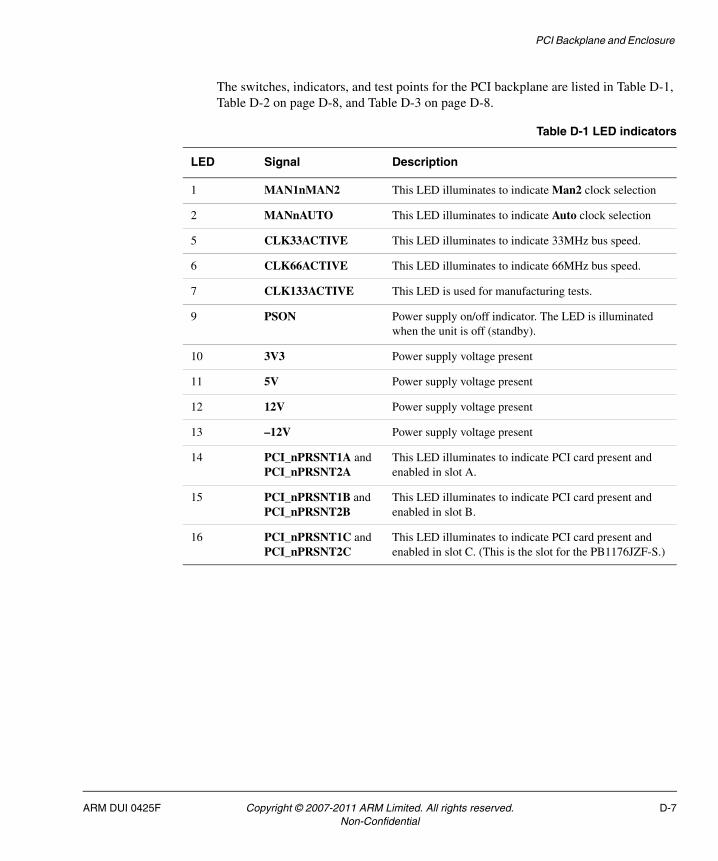
PCI Backplane and Enclosure
The switches, indicators, and test points for the PCI backplane are listed in Table D-1, Table D-2 on page D-8, and Table D-3 on page D-8.
Table D-1 LED indicators
LED Signal Description
1 MAN1nMAN2 This LED illuminates to indicate Man2 clock selection
2 MANnAUTO This LED illuminates to indicate Auto clock selection
5 CLK33ACTIVE This LED illuminates to indicate 33MHz bus speed.
6 CLK66ACTIVE This LED illuminates to indicate 66MHz bus speed.
7 CLK133ACTIVE This LED is used for manufacturing tests.
9 PSON Power supply on/off indicator. The LED is illuminated when the unit is off (standby).
10 3V3 Power supply voltage present
11 5V Power supply voltage present
12 12V Power supply voltage present
13 –12V Power supply voltage present
14 PCI_nPRSNT1A and PCI_nPRSNT2A
This LED illuminates to indicate PCI card present and enabled in slot A.
15 PCI_nPRSNT1B and PCI_nPRSNT2B
This LED illuminates to indicate PCI card present and enabled in slot B.
16 PCI_nPRSNT1C and PCI_nPRSNT2C
This LED illuminates to indicate PCI card present and enabled in slot C. (This is the slot for the PB1176JZF-S.)
ARM DUI 0425F Copyright © 2007-2011 ARM Limited. All rights reserved. D-7Non-Confidential

PCI Backplane and Enclosure
Table D-2 Configuration switches
Switch Signal Description
SW1-1 MAN1nMAN2 Determines the clock rate when SW1[1] is in the Manual position. See Setting the backplane configuration switches on page D-4.
SW1-2 MANnAUTO Selects between manual (ON) or automatic (OFF) clock selection
SW2-1 nINCPLD Omits (ON) or includes (OFF) the PLD in the scan chain.
SW2-2 TESTnEN Omits (ON) or includes (OFF) the PCI sockets in the scan chain.
Table D-3 Power and reset switches
Switch Signal Description
SW3 PSON Power on/off pushbutton. Pressing the switch toggles the power between on and standby. SW3 signals are also connected to J6 and this enables the use of an external front-panel switch.
SW4 SYSTEM_nRESET System reset pushbutton. Pressing the switch generates a reset to the PCI arbiter on the backplane and all of the PCI cards. SW4 signals are also connected to J7 and this enables the use of an external front-panel switch.
Table D-4 Test points
Test point Signal Description
TP1 GND Ground
TP2 GND Ground
TP3 TCLK JTAG clock
TP4 PCI CLK PCI clock
D-8 Copyright © 2007-2011 ARM Limited. All rights reserved. ARM DUI 0425FNon-Confidential
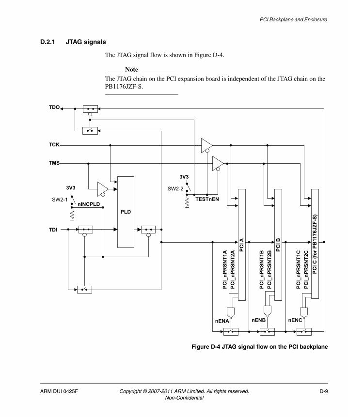
PCI Backplane and Enclosure
D.2.1 JTAG signals
The JTAG signal flow is shown in Figure D-4.
Note The JTAG chain on the PCI expansion board is independent of the JTAG chain on the PB1176JZF-S.
Figure D-4 JTAG signal flow on the PCI backplane
PLD
TESTnEN
TMS
TDO
TDI
TCK
PCI C
(for
PB
1176
JZF-
S)
PCI B
PCI A
nENA nENB nENC
nINCPLD
3V3
SW2-23V3
PCI_
nPR
SNT2
BPC
I_nP
RSN
T1B
PCI_
nPR
SNT2
CPC
I_nP
RSN
T1C
PCI_
nPR
SNT2
APC
I_nP
RSN
T1A
SW2-1
ARM DUI 0425F Copyright © 2007-2011 ARM Limited. All rights reserved. D-9Non-Confidential
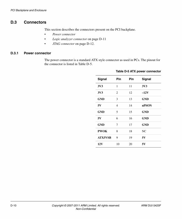
PCI Backplane and Enclosure
D.3 Connectors
This section describes the connectors present on the PCI backplane.
• Power connector
• Logic analyzer connector on page D-11
• JTAG connector on page D-12.
D.3.1 Power connector
The power connector is a standard ATX style connector as used in PCs. The pinout for the connector is listed in Table D-5.
Table D-5 ATX power connector
Signal Pin Pin Signal
3V3 1 11 3V3
3V3 2 12 –12V
GND 3 13 GND
5V 4 14 nPSON
GND 5 15 GND
5V 6 16 GND
GND 7 17 GND
PWOK 8 18 NC
ATX5VSB 9 19 5V
12V 10 20 5V
D-10 Copyright © 2007-2011 ARM Limited. All rights reserved. ARM DUI 0425FNon-Confidential

PCI Backplane and Enclosure
D.3.2 Logic analyzer connector
Figure D-5 and Table D-6 show the pinout of the Mictor connector J4. You can use this connector to monitor PCI signals on the backplane.
Note Agilent (formerly HP) and Tektronix label these connectors differently, but the assignments of signals to physical pins is appropriate for both systems and pin 1 is always in the same place.
Figure D-5 AMP Mictor connector J4
Table D-6 Mictor connector pinout
Channel Pin Pin Channel
No connect 1 2 No connect
GND 3 4 No connect
PCI_CLKE 5 6 No connect
PCI_nIRDY 7 8 No connect
PCI_nTDRY 9 10 No connect
PCI_nINTD 11 12 No connect
PCI_nINTC 13 14 SYSTEM_nRESET
PCI_nINTB 15 16 PCI_PAR64
PCI_nINTA 17 18 PCI_nSERR
PCI_nGNTC 19 20 PCI_nPERR
PCI_nGNTB 21 22 PCI_nACK64
PCI_nGNTA 23 24 PCI_nREQ64
PCI_nREQC 25 26 PCI_M66EN
1
2
37
38
ARM DUI 0425F Copyright © 2007-2011 ARM Limited. All rights reserved. D-11Non-Confidential
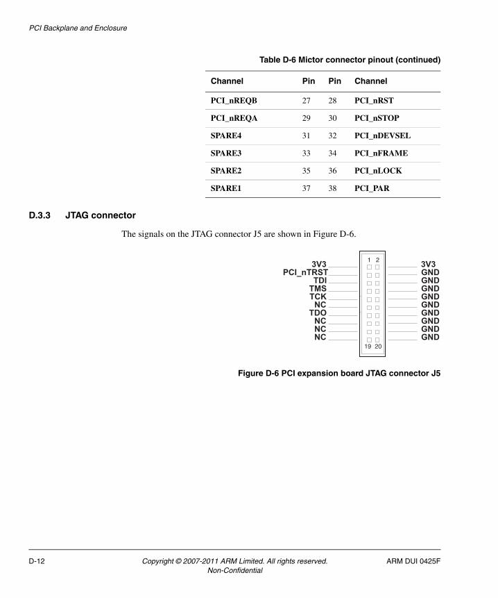
PCI Backplane and Enclosure
D.3.3 JTAG connector
The signals on the JTAG connector J5 are shown in Figure D-6.
Figure D-6 PCI expansion board JTAG connector J5
PCI_nREQB 27 28 PCI_nRST
PCI_nREQA 29 30 PCI_nSTOP
SPARE4 31 32 PCI_nDEVSEL
SPARE3 33 34 PCI_nFRAME
SPARE2 35 36 PCI_nLOCK
SPARE1 37 38 PCI_PAR
Table D-6 Mictor connector pinout (continued)
Channel Pin Pin Channel
3V33V3GNDGNDGNDGNDGNDGNDGNDGNDGND
PCI_nTRSTTDI
TMSTCK
NCTDO
NCNCNC
1
19
2
20
D-12 Copyright © 2007-2011 ARM Limited. All rights reserved. ARM DUI 0425FNon-Confidential

Appendix E Memory Expansion Boards
This appendix describes expansion memory modules for the PB1176JZF-S. It contains the following sections:
• About memory expansion on page E-2
• Fitting a memory board on page E-4
• Connector pinout on page E-5.
ARM DUI 0425F Copyright © 2007-2011 ARM Limited. All rights reserved. E-1Non-Confidential

Memory Expansion Boards
E.1 About memory expansion
Only static memory expansion is supported by the PB1176JZF-S. You can stack static memory expansion boards on the PB1176JZF-S using the PISMO™ connector provided. There are five chip select signals available on the PISMO connector, each of these can select 64MB of SRAM. The distribution of the chip select signals is determined by the expansion memory boards themselves.
The block diagram for typical memory board is shown in Figure E-1.
Figure E-1 Static memory board block diagram
Exp
ansi
on c
onne
ctor
PISMO expansion module
SMAADD[25:0] and control signals
SMDATA[31:0]
CSWIDTH1
CSWIDTH0
SBSCLSBSDA EEPROM
3V3
GND
CSWIDTHselect link
Static memory
Chip select links
nCS0
nCS4
nCS3
nCS2
nCS1
Reserved
E-2 Copyright © 2007-2011 ARM Limited. All rights reserved. ARM DUI 0425FNon-Confidential

Memory Expansion Boards
Note Figure E-1 on page E-2 is only a typical example of a PISMO static memory expansion board, different expansion boards might have different features.
See the documentation provided with your memory board for details on specific signals and link options.
The PB1176JZF-S supports static memory modules compliant to the Platform Independent Storage MOdule (PISMO) specification Version 1.0. General information and specifications are available from the PISMO website: www.pismoworld.org.
E.1.1 Operation without expansion memory
You can operate the PB1176JZF-S without a memory expansion board connected because it has 8MB of pseudo SRAM, 128MB of SDRAM, and 128MB of NOR flash permanently fitted.
E.1.2 Memory board configuration
The PISMO memory module includes a configuration EEPROM that can be read from the PB1176JZF-S to identify the type of memory on the board and how it is configured. This information can be used by the application or operating system to initialize the memory space. For details of the EEPROM data structure and information elements see the PISMO Specification Version 1.0.
Note 1V8 to 3V3 cards are supported.
ARM DUI 0425F Copyright © 2007-2011 ARM Limited. All rights reserved. E-3Non-Confidential

Memory Expansion Boards
E.2 Fitting a memory board
To install a memory expansion board:
1. Ensure that the PB1176JZF-S is powered down.
2. Align the memory expansion board with the PISMO connector on the PB1176JZF-S. See About the PB1176JZF-S on page 1-2 for the location of the PISMO connector.
3. Press the module into the connector.
4. Stack additional modules as required (up to five modules may be stacked) using the mating connectors on the PISMO memory modules.
E-4 Copyright © 2007-2011 ARM Limited. All rights reserved. ARM DUI 0425FNon-Confidential

Memory Expansion Boards
E.3 Connector pinout
This section describes the connector present on the expansion memory board.
Caution The pinout and naming in Table E-1 are valid for the PISMO Version 1.0 specification.
The PB1176JZF-S memory expansion port is not compatible with the PISMO2 Version 1.0 specification.
E.3.1 Expansion connector
The static memory expansion board uses 120-way Samtec connector as shown in Figure E-2. The connector pinout is shown in Table E-1.
Note The numbering of pins on the connector is for the connector as viewed from below.
Figure E-2 Samtec QSH 120-way static expansion connector
2
1 59
60
61
62 120
119
Table E-1 Static memory connector signals
Pin No. Signal Pin No. Signal
1 DATA[0] 2 3V3
3 DATA[1] 4 3V3
5 DATA[2] 6 3V3
7 DATA[3] 8 3V3
9 DATA[4] 10 VDDIOa
11 DATA[5] 12 VDDIOa
ARM DUI 0425F Copyright © 2007-2011 ARM Limited. All rights reserved. E-5Non-Confidential

Memory Expansion Boards
13 DATA[6] 14 VDDIOa
15 DATA[7] 16 VDDIOa
17 DATA[8] 18 1V8
19 DATA[9] 20 1V8
21 DATA[10] 22 1V8
23 DATA[11] 24 1V8
25 DATA[12] 26 NC
27 DATA[13] 28 Reserved, not driven
29 DATA[14] 30 Reserved, not driven
31 DATA[15] 32 Reserved, not driven
33 DATA[16] 34 5V
35 DATA[17] 36 5V
37 DATA[18] 38 5V
39 DATA[19] 40 5V
41 DATA[20] 42 Reserved, not driven
43 DATA[21] 44 Reserved, not driven
45 DATA[22] 46 Reserved, not driven
47 DATA[23] 48 Reserved, not driven
49 DATA[24] 50 Reserved, not driven
51 DATA[25] 52 Reserved, not driven
53 DATA[26] 54 Reserved, not driven
55 DATA[27] 56 Reserved, not driven
57 DATA[28] 58 Reserved, not driven
59 DATA[29] 60 Reserved, not driven
Table E-1 Static memory connector signals (continued)
Pin No. Signal Pin No. Signal
E-6 Copyright © 2007-2011 ARM Limited. All rights reserved. ARM DUI 0425FNon-Confidential

Memory Expansion Boards
61 DATA[30] 62 SBSCL, E2PROM serial interface clock (3.3V signal level)
63 DATA[31] 64 SBSDA, E2PROM serial interface data (3.3V signal level)
65 ADDR[0] 66 nRESET
67 ADDR[1] 68 nBOARDPOR, asserted on hardware power cycle
69 ADDR[2] 70 nFLWP, flash write protect. Drive HIGH to write to flash.
71 ADDR[3] 72 nEARLYRESET, Reset signal. Differs from nRESET in that it is not delayed by nWAIT.
73 ADDR[4] 74 nWAIT, Wait mode input from external memory controller. Pulled HIGH if not used.
75 ADDR[5] 76 nBURSTWAIT, Synchronous burst wait input. The external device uses this to delay a synchronous burst transfer if LOW. Pulled HIGH if not used.
77 ADDR[6] 78 CANCELWAIT, If HIGH, this signal enables the system to recover from an externally waited transfer that has taken longer than expected to finish. Pulled LOW if not used.
79 ADDR[7] 80 nCS[4]
81 ADDR[8] 82 nCS[3]
83 ADDR[9] 84 nCS[2]
85 ADDR[10] 86 nCS[1]
87 ADDR[11] 88 Reserved, not driven
89 ADDR[12] 90 Reserved, not driven
91 ADDR[13] 92 Reserved, not driven
Table E-1 Static memory connector signals (continued)
Pin No. Signal Pin No. Signal
ARM DUI 0425F Copyright © 2007-2011 ARM Limited. All rights reserved. E-7Non-Confidential

Memory Expansion Boards
93 ADDR[14] 94 Reserved, not driven
95 ADDR[15] 96 nCS[0]
97 ADDR[16] 98 nBUSY, Indicates that memory is not ready to be released from reset. If LOW, this signal holds nRESET active.
99 ADDR[17] 100 nIRQ
101 ADDR[18] 102 nWEN
103 ADDR[19] 104 nOEN
105 ADDR[20] 106 nBLS[3], Byte Lane Select for bits [31:24]
107 ADDR[21] 108 nBLS[2], Byte Lane Select for bits [23:16]
109 ADDR[22] 110 nBLS[1], Byte Lane Select for bits [15:8]
111 ADDR[23] 111 nBLS[0], Byte Lane Select for bits [7:0]
113 ADDR[24] 114 CSWIDTH[0], Indicates bus width for fitted part. Not routed through stackable boards.
115 ADDR[25] 116 CSWIDTH[1], Indicates bus width for fitted part. Not routed through stackable boards.
117 ADDRVALID, Indicates that the address output is stable during synchronous burst transfers
118 CLK[1]
119 BAA, Burst Address Advance. Used to advance the address count in the memory device
120 CLK[0]
a. VDDIO is the data voltage to host. This is not routed through stackable boards
Table E-1 Static memory connector signals (continued)
Pin No. Signal Pin No. Signal
E-8 Copyright © 2007-2011 ARM Limited. All rights reserved. ARM DUI 0425FNon-Confidential
Appendix F Boot Monitor and platform library
This appendix describes using the Boot Monitor and platform library provided with the PB1176JZF-S. It contains the following sections:
• About the Boot Monitor on page F-2
• About the platform library on page F-3
• Using the baseboard Boot Monitor and platform library on page F-4.
ARM DUI 0425F Copyright © 2007-2011 ARM Limited. All rights reserved. F-1Non-Confidential
Boot Monitor and platform library
F.1 About the Boot Monitor
This is the standard ARM application that runs when the system is booted. It is built with the ARM platform library.
Note Any application that is built using the ARM platform library (or handles its own initialization) can replace the Boot Monitor.
The Boot Monitor supports the following functions:
• general file operations
• MMC and SD card utilities. This performs FAT16 format up to 2GB.
• board configuration
• programming images into flash memory
• loading and running another application
• a semihost server that handles standard ARM semihosting SVC calls.
F-2 Copyright © 2007-2011 ARM Limited. All rights reserved. ARM DUI 0425FNon-Confidential

Boot Monitor and platform library
F.2 About the platform library
The ARM platform library handles the system initialization and re-targets the standard C library. To achieve this, it provides a basic I/O subsystem that supports simple device drivers.
Included with the platform library there is a simple terminal driver, UART, PS/2 keyboard and LCD drivers and support for semihosting I/O.
ARM DUI 0425F Copyright © 2007-2011 ARM Limited. All rights reserved. F-3Non-Confidential
Boot Monitor and platform library
F.3 Using the baseboard Boot Monitor and platform library
The baseboard Boot Monitor is a collection of tools and utilities designed as an aid to developing applications on the baseboard.
When the Boot Monitor starts on reset, the following actions are performed:
• the memory controllers are initialized
• a stack is set up in memory
• Boot Monitor code is copied into DRAM
• Boot memory remapping is reset
• C library I/O routines are remapped and redirected depending on the settings of User Switches 2 and 3 (S6-2 and S6-3 on the baseboard).
• if Boot Monitor configuration switch User Switch 1 (S6-1 on the baseboard) is ON, the current boot script, if any, is run.
Note The boot monitor defaults to booting in secure mode after reset.
Caution The firmware must match the system configuration or the results might be unpredictable. See the application note for your configuration for details of software or firmware that is specific to the combination of baseboard and tiles that you are using.
The following section describes:
• Boot Monitor configuration switches on page F-5
• Running the Boot Monitor on page F-6
• Loading Boot Monitor into NOR flash on page F-7
• Redirecting character output to hardware devices on page F-8
• Using a boot script to run an image automatically on page F-8
• Rebuilding the Boot Monitor or platform library on page F-9
• Building an application with the platform library on page F-10
• Building an application that uses semihosting on page F-13
• Loading and running an application from NOR flash on page F-13
• Running an image from MMC or SD card on page F-15
• Using the Network Flash Utility on page F-15.
F-4 Copyright © 2007-2011 ARM Limited. All rights reserved. ARM DUI 0425FNon-Confidential
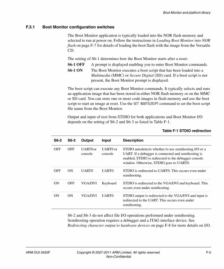
Boot Monitor and platform library
F.3.1 Boot Monitor configuration switches
The Boot Monitor application is typically loaded into the NOR flash memory and selected to run at power on. Follow the instructions in Loading Boot Monitor into NOR flash on page F-7 for details of loading the boot flash with the image from the Versatile CD.
The setting of S6-1 determines how the Boot Monitor starts after a reset:
S6-1 OFF A prompt is displayed enabling you to enter Boot Monitor commands.
S6-1 ON The Boot Monitor executes a boot script that has been loaded into a Multimedia (MMC) or Secure Digital (SD) card. If a boot script is not present, the Boot Monitor prompt is displayed.
The boot script can execute any Boot Monitor commands. It typically selects and runs an application image that has been stored in either NOR flash memory or on the MMC or SD card. You can store one or more code images in flash memory and use the boot script to start an image at reset. Use the SET BOOTSCRIPT command to set the boot script file name from the Boot Monitor.
Output and input of text from STDIO for both applications and Boot Monitor I/O depends on the setting of S6-2 and S6-3 as listed in Table F-1.
S6-2 and S6-3 do not affect file I/O operations performed under semihosting. Semihosting operation requires a debugger and a JTAG interface device. See Redirecting character output to hardware devices on page F-8 for more details on I/O.
Table F-1 STDIO redirection
S6-2 S6-3 Output Input Description
OFF OFF UART0 or console
UART0 or console
STDIO autodetects whether to use semihosting I/O or a UART. If a debugger is connected and semihosting is enabled, STDIO is redirected to the debugger console window. Otherwise, STDIO goes to UART0.
OFF ON UART0 UART0 STDIO is redirected to UART0. This occurs even under semihosting.
ON OFF VGA/DVI Keyboard STDIO is redirected to the VGA/DVI and keyboard. This occurs even under semihosting.
ON ON VGA/DVI UART0 STDIO output is redirected to the VGA/DVI and input is redirected to the UART. This occurs even under semihosting.
ARM DUI 0425F Copyright © 2007-2011 ARM Limited. All rights reserved. F-5Non-Confidential

Boot Monitor and platform library
Note Switches S6-4 to S6-8 are not used by the Boot Monitor and are available for user applications.
If a different loader program is present at the boot location, the function of the entire S6 switch bank is implementation dependent.
F.3.2 Running the Boot Monitor
To run Boot Monitor and have it display a prompt to a terminal connected to UART0, set switches S6-1 to S6-3 to OFF and reset the system. Standard input and output functions use UART0 by default. The default setting for UART0 is 38400 baud, 8 data bits, no parity, 1 stop bit. There is no hardware or software flow control. Use these values to configure a terminal application on your PC to communicate with the Boot Monitor.
Note If the Boot Monitor has been accidently deleted from flash memory, see Rebuilding the Boot Monitor or platform library on page F-9 for information on loading the monitor.
Boot Monitor commands
See Appendix G Boot Monitor Commands for details of the available commands in Version 4 of the Boot Monitor.
Commands are accepted in uppercase or lowercase. The Boot Monitor accepts abbreviations of commands if the meaning is not ambiguous. For example, for QUIT, you can type QUIT, QUI, QU, Q, quit, qui, qu, or q.
Optional parameters for commands are indicated by []. For example DIRECTORY [directory] indicates that the DIRECTORY command can take an optional parameter to specify which directory to list the contents of. If no parameter is supplied, the default is used (in this case, the current directory).
Type HELP at the Boot Monitor prompt to display a full list of the available commands.
F-6 Copyright © 2007-2011 ARM Limited. All rights reserved. ARM DUI 0425FNon-Confidential

Boot Monitor and platform library
F.3.3 Loading Boot Monitor into NOR flash
If the flash becomes corrupt and the board no longer runs the Boot Monitor, the Boot Monitor must be reprogrammed into flash.
Because the debugger does not initialize DRAM, the Boot Monitor image cannot be loaded and run directly. Boot from the AXI expansion memory as described in Table 2-1 on page 2-4. This procedure automatically configures the DRAM:
1. Power off the board.
2. Set the configuration switches:
• Set all S6 switches to OFF
• Set S7-2 switch to ON
• Set S7-1, 3, and 4 to OFF.
3. Connect a cable from the JTAG device (RealView ICE for example) to the JTAG box header.
4. Power on the board.
5. DRAM is now initialized by booting from AXI expansion memory and the memory is remapped. To load Boot Monitor into flash:
a. From the debugger, load and execute the file Boot_Monitor.axf
b. at the Boot Monitor prompt enter:>FLASH
Erase any images already in Flash using the ERASE IMAGE command.Flash> WRITE IMAGE path\Boot_Monitor_platform.axf
where path is the path to the version of the Boot Monitor that is being loaded and platform is the name of the target system.
6. Loading the image into flash takes a few minutes to complete. Wait until the prompt is displayed again before proceeding.
7. Turn the board off.
8. Set S7-2 to OFF.
9. Turn the board back on.
Boot Monitor starts automatically.
ARM DUI 0425F Copyright © 2007-2011 ARM Limited. All rights reserved. F-7Non-Confidential

Boot Monitor and platform library
F.3.4 Redirecting character output to hardware devices
The redirection of character I/O is carried out within the Boot Monitor platform library routines in retarget.c and boot.s. During startup, the platform library executes a SuperVisor Call (SVC). If the image is being executed without a debugger (or the debugger is not capturing semihosting calls) the value returned by this SVC is –1, otherwise the value returned is positive. The platform library uses the return value to determine the hardware device used for outputting from the C library I/O functions. (Redirection is through a SVC to the debugger console or directly to a hardware device)
Supported devices for character output are:
• :UART-0 (default destination if debugger is not capturing semihosting calls)
• :UART-1
• :UART-2
• :UART-3
• :CHARLCD.
The STDIO calls are redirected within retarget.c. Redirection depends on the setting of switches S6-2 and S6-3, see Boot Monitor configuration switches on page F-5 for details.
F.3.5 Using a boot script to run an image automatically
Use a boot script to run an image automatically after power-on:
1. Create a boot script in a MMC or SD Card from the Boot Monitor by typing:
• if your image is in MMC or SD Card:M:\> CREATE myscript.txt; put any startup code here RUN path\file_name
• if your image is in NOR flash:M:\> CREATE myscript.txt; put any startup code here FLASH RUN file_name.
2. Press Ctrl-Z to indicate the end of the boot script and return to the Boot Monitor prompt.
Note RVD does not support Ctrl-Z when creating a boot script using the debugger. You
must instead type +++ on a new line to indicate the end of a boot script.
3. Verify the file was entered correctly by typing:
M:\>TYPE myscript.txt
The contents of the file is displayed to the currently selected output device.
F-8 Copyright © 2007-2011 ARM Limited. All rights reserved. ARM DUI 0425FNon-Confidential

Boot Monitor and platform library
4. Specify the boot script to use at reset from the Boot Monitor by typing:
M:\>SET BOOTSCRIPT myscript.txt
5. Set S6-1 ON to instruct the Boot Monitor to run the boot script at power on.
6. Reset the platform. The Boot Monitor runs and executes the boot script myscript.txt. In this case, it relocates the image file_name and executes it.
F.3.6 Rebuilding the Boot Monitor or platform library
All firmware components are built using either RVDS running under either Windows or Unix/Linux:
• For Windows, ARM RVDS can be used to rebuild the library.
Use a CodeWarrior project file to rebuild the library. The RVDS make utility is not supported.
• GNUmake is available for UNIX and Linux.
If you are using GNUmake to rebuild the Boot Monitor, set your default directory to install_directory/Firmware/Boot_Monitor and type make from a command shell.
To rebuild the platform library component, set your default directory to install_directory/Firmware/platform and type make from a command shell.
After rebuilding the Boot Monitor, load it into NOR flash, see Loading Boot Monitor into NOR flash on page F-7.
After rebuilding the platform library, you can link platform.a from the target build subdirectories with your application (see Building an application with the platform library on page F-10).
Build options
You can specify the following build options after the make command:
• BIG_ENDIAN=1/0, defining image endianness (Default 0, little endian)
• THUMB=1/0, defining image state (Default 0, ARM)
• DEBUG=1/0, defining optimization level (Default 0, optimized code)
• VFP=1/0, defines VFP support (Default 0, no VFP support).
Note The Boot Monitor must be built as a simple image. Scatter loading is not supported.
ARM DUI 0425F Copyright © 2007-2011 ARM Limited. All rights reserved. F-9Non-Confidential

Boot Monitor and platform library
The build options define the subdirectory in the Builds directory that contains the compile and link output:
<Debug>_<State>_<Endianness>_Endian + more component specific options
For example, Release_ARM_Little_Endian or Debug_Thumb_Big_Endian.
The makefile creates a directory called Builds if it is not already present. The Builds directory contains subdirectories for the specified make options (for example, Debug_ARM_Little_Endian). To delete the objects and images for all targets and delete the Builds directory, type make clean all.
F.3.7 Building an application with the platform library
The platform library on the CD provides all required initialization code to bring the baseboard up from reset. The library is used by the Boot Monitor, but it can be used by an application independent of the other code in the Boot Monitor.
Note It is not necessary to build your application with the platform library. You can instead let the boot monitor run at power on and remap the memory. After the remap has finished, you can load a typical application built with RVDS that is linked at address 0x8000 and uses semihosting.
The platform library supports:
• remapping of boot memory
• DRAM initialization
• UARTs
• Time-of-Year clock
• output to the character LCD display
• C library system calls.
To build an image that uses the I/O and memory control features present in the platform library:
1. Write the application as normal. There must be a main() routine in the application.
Linking an application with the platform requires that the application is built using RVCT V2.1 or greater. If you are using RVCT V2.0 or ADS it is not possible to link the application with the platform library, however an application can still utilize the hardware on the board through semihosting.
F-10 Copyright © 2007-2011 ARM Limited. All rights reserved. ARM DUI 0425FNon-Confidential

Boot Monitor and platform library
2. Link the application against the Boot Monitor platform library file platform.a. The file platform.a is in one of the target build subdirectories (install_dir\software\firmware\Platform\Builds\target_build).
Choose the Builds subdirectory that matches your application. For example, Release_ARM_Little_Endian for ARM code. If the subdirectory does not exist, see Rebuilding the Boot Monitor or platform library on page F-9 for details on rebuilding platform.a.
Note If you are not using the platform.a library, you must provide your own
initialization and I/O routines.
You can also build the platform library functionality directly into your application without building the platform code as a separate library. This might be useful, for example, if you are using an IDE to develop your application.
See the filelist.txt file in the software directory for more details on software included on the CD. The selftest directory, for example, contains source files that can be used as a starting point for your own application.
3. If required, select the link time selection for the platform library options.
Platform selection uses special symbols in your application:
From C #pragma import(_platform_option_xxxxx)
From assembler IMPORT _platform_option_xxxxx
The platform options are listed in Table F-2.
4. Scatter loading is supported for applications using the platform library, however the scatter file must follow Example F-1 on page F-12. The execution regions INIT and SDRAM must be present, the execution regions ITCM and DTCM are optional, if they are present, the relevant Tightly Coupled Memory (TCM) is enabled and the base address is set to the address supplied in the scatter file. The
Table F-2 platform library options
Option Description
_platform_option_no_cache Stops the cache from being enabled by default
_platform_option_no_lcd_kbd Disables LCD & Keyboard support and stops the driver code from being loaded
_platform_option_no_mmu Stops the MMU from being initialized by default.
ARM DUI 0425F Copyright © 2007-2011 ARM Limited. All rights reserved. F-11Non-Confidential

Boot Monitor and platform library
sys_vectors.o object must be located at address zero. Additional execution regions, such as one for the SSRAM, can be added. An example scatter loading application can be found in the examples directory.
Example F-1 Scatter loading
LR_ROOT 0x8000{ INIT +0 FIXED { sys_boot.o (!!!_platform_area_boot, +FIRST) *(+RO) } SDRAM +0 { *(+RW,+ZI) } ITCM 0x0 { sys_vectors.o(_platform_area_vectors, +FIRST) ‘application code’.o(+RO) } DTCM 0x08000000 { ‘application code’.o(+RW,+ZI) }}
5. To run the image from RAM, load the image with a debugger and execute as normal. The image uses the procedure described in Redirecting character output to hardware devices on page F-8 to redirect standard I/O either to the debugger or to be handled by the application itself.
See Loading and running an application from NOR flash on page F-13 for more information on running from flash.
Note If the platform library encounters a fatal error, all the user LEDs flash at a one-second interval and an error message is output on UART-0.
F-12 Copyright © 2007-2011 ARM Limited. All rights reserved. ARM DUI 0425FNon-Confidential

Boot Monitor and platform library
F.3.8 Building an application that uses semihosting
The boot monitor handles semihosting SWIs the same as a debugger handles SWIs. This enables an image that is not linked against with the platform library to be loaded into flash memory and have the boot monitor manage the I/O.
All I/O using stdio(), for example printf(), uses the same devices as the boot monitor console (either UART-0 or the Keyboard/LCD depending on the Boot Monitor configuration switch settings). File functions access the flash and character I/O devices using the mechanisms described in Redirecting character output to hardware devices on page F-8. For example, open the character LCD by using the special file name: CHARLCD.
There are no specific tools requirements. Images built with RealView tools must run if they are built to use semihosting. This means that an image built using the tool kit defaults can be loaded onto the baseboard and run.
F.3.9 Loading and running an application from NOR flash
To run an image from NOR flash:
1. Build the application as described in Building an application with the platform library on page F-10 and specify a link address suitable for flash. There are the following options for selecting the address:
Load region in flash The image is linked so that its load region, though not necessarily its execution region, is in flash. The load region specified when the image was linked is used as the location in flash and the FLASH_ADDRESS option is ignored. If the blocks in flash are not free, the command fails. Use the FLASH RUN command to run the image.
Load region not in flash and image location not specified The image is programmed into the first available contiguous set of blocks in flash that is large enough to hold the image. Use the FLASH LOAD and then the FLASH RUN commands to load and run the image.
Load region not in flash, but image stored at a specified flash address Use the FLASH_ADDRESS option to specify the location of the image in flash. If the option is not used, the image is programmed into the first available contiguous set of blocks in flash that is large enough to hold the image. Use the FLASH LOAD or FLASH RUN commands to load and run the image.
ARM DUI 0425F Copyright © 2007-2011 ARM Limited. All rights reserved. F-13Non-Confidential

Boot Monitor and platform library
Note Images with multiple load regions are not supported.
If the image is loaded into flash, but the FLASH RUN command relocates code to DRAM for execution, the execution address must not be in the top 4MBytes of DRAM because the Boot Monitor uses this.
2. The image must be programmed into flash using the Boot Monitor. Flash support is implemented in the Boot Monitor image.
Run the Boot Monitor image from the debugger and enter the flash subsystem, type FLASH at the prompt:
>FLASHflash>
3. The command used to program the image depends on the type of image:
• The entry point and load address for ELF images are taken from the image itself. To program the ELF image into flash, use the following command line:flash> WRITE IMAGE elf_file_name NAME name FLASH_ADDRESS address
• The entry point and load address for ELF images are taken from the command line options. To program a binary image into flash, use the following command line:flash> WRITE BINARY image_file_name NAME name FLASH_ADDRESS address1LOAD_ADDRESS address2 ENTRY_POINT address3
Note name is a short name for the image. If the NAME option is not used at the command
prompt, then name is derived from the file name.
4. The image is now in flash and can be run by the Boot Monitor. At the prompt, type:
flash> RUN name
F-14 Copyright © 2007-2011 ARM Limited. All rights reserved. ARM DUI 0425FNon-Confidential

Boot Monitor and platform library
F.3.10 Running an image from MMC or SD card
To run an image from the MMC or SD card:
1. Build and link the application as described in Loading and running an application from NOR flash on page F-13.
Note Images with multiple load regions are not supported.
The image must have an execution region in RAM or DRAM.
The execution address must not be in the top 4MBytes of DRAM because the Boot Monitor uses this area.
2. The image must be programmed into MMC or SD card using the Boot Monitor.
Connect a debugger and use semihosting to load the file:
>COPY C:\software\elf_file_name file_name
3. To run the image manually, from the debugger, or terminal connected to UART0, type:
>RUN file_name
F.3.11 Using the Network Flash Utility
This utility uses the TFTP protocol to access files over the Ethernet network. You can use this utility to program files into flash.
To connect to a server and program a file to flash:
1. Start the NFU utility from the debugger console:
a. Set the on setting the Boot Monitor configuration switches to force the console to use either UART-0 or the LCD and keyboard. (See Boot Monitor configuration switches on page F-5 for details.)
Note The debugger console cannot be used because the semihosted console I/O
is blocking.
b. Start the NFU utility.
Note It typically takes several seconds for NFU start. Do not enter any commands
until the prompt is displayed.
ARM DUI 0425F Copyright © 2007-2011 ARM Limited. All rights reserved. F-15Non-Confidential

Boot Monitor and platform library
2. Use the DHCP protocol to get an IP address by entering:
manage dhcpc start
3. Use the map command to map a drive letter to the TFTP server. For example to access a file on a TFTP server with the IP address 192.168.0.1, use:
manage map n: 192.168.0.1
4. After the drive letter has been mapped, use the normal Boot Monitor command on the remote file by specifying the drive letter. For example, to write a file to DOC, enter:
flash write image n:/hello.axf
NFU commands
The NFU supports a subset of the standard Boot Monitor commands and adds a new MANAGE sub-menu.
The NFU commands are listed in Table F-3.
Table F-3 NFU commands
Command Action
CD directory path Change directory
CONVERT BINARY binary_file LOAD_ADDRESS address [ENTRY_POINT address]
Provides information to the system that is required by the RUN command to execute a binary file. A new file with name binary_file is produced, but with an.exe file extension.
COPY file1 file2 Copy file1 to file2. For example, to copy the leds code from the PC to the flash enter: COPY C:\software\projects\examples\rvds2.0\leds.axf leds.axf
Note Remote file access requires semihosting. Use a debugger connection to provide semihosting.
CREATE filename Create a new file in the flash by inputting text. Press Ctrl-Z to end the file.
DELETE filename Delete file from flash.
DIRECTORY [directory] List the files in a directory.
Files that only accessible from semihosting cannot be listed.
F-16 Copyright © 2007-2011 ARM Limited. All rights reserved. ARM DUI 0425FNon-Confidential
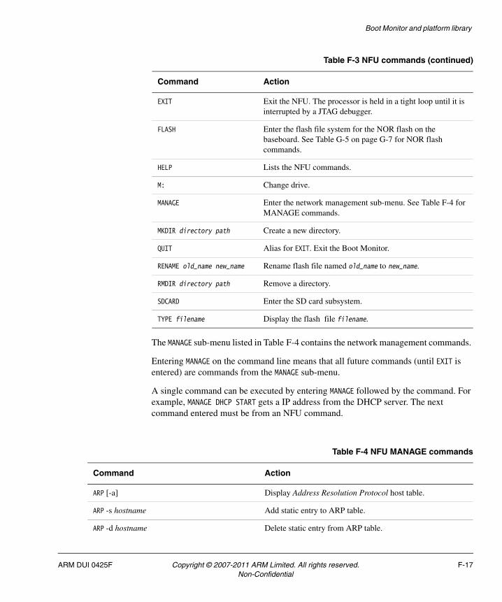
Boot Monitor and platform library
The MANAGE sub-menu listed in Table F-4 contains the network management commands.
Entering MANAGE on the command line means that all future commands (until EXIT is entered) are commands from the MANAGE sub-menu.
A single command can be executed by entering MANAGE followed by the command. For example, MANAGE DHCP START gets a IP address from the DHCP server. The next command entered must be from an NFU command.
EXIT Exit the NFU. The processor is held in a tight loop until it is interrupted by a JTAG debugger.
FLASH Enter the flash file system for the NOR flash on the baseboard. See Table G-5 on page G-7 for NOR flash commands.
HELP Lists the NFU commands.
M: Change drive.
MANAGE Enter the network management sub-menu. See Table F-4 for MANAGE commands.
MKDIR directory path Create a new directory.
QUIT Alias for EXIT. Exit the Boot Monitor.
RENAME old_name new_name Rename flash file named old_name to new_name.
RMDIR directory path Remove a directory.
SDCARD Enter the SD card subsystem.
TYPE filename Display the flash file filename.
Table F-3 NFU commands (continued)
Command Action
Table F-4 NFU MANAGE commands
Command Action
ARP [-a] Display Address Resolution Protocol host table.
ARP -s hostname Add static entry to ARP table.
ARP -d hostname Delete static entry from ARP table.
ARM DUI 0425F Copyright © 2007-2011 ARM Limited. All rights reserved. F-17Non-Confidential

Boot Monitor and platform library
DHCPC START ifname Use Dynamic Host Configuration Protocol (DHCP) to start a connection with the network interface ifname.
DHCPC RELEASE ifname Use DHCP to release the connection with the network interface ifname.
DHCPC SIZEOF Returns information on the size of the DHCP packet.
DHCP INFORM ifname ip_address Uses the DHCP protocol send information to the server located at ip_address with the network interface ifname.
EXIT Exit the MANAGE sub-menu. The commands listed in Table F-3 on page F-16 can be entered at the NFU prompt.
HELP Lists the NFU MANAGE commands.
IFCONFIG Displays the IP settings that are used for communications with the server.
IFCONFIG [ifname [ip_address]] Displays the current IP address if ip_address is not suppled. Otherwise, the current IP address for the interface ifname is set to ip_address.
IFCONFIG [ifname [option]] Configures the IP interface ifname. The value for option can be:
netmask maskvalue set the netmask
dstaddr address set the destination IP address
mtu n set the maximum transfer unit
up activate the interface
down shutdown the interface
MAP drive address Maps the IP address specified in address to drive.
NETSTAT [-option] Displays active network connections. The value for option can be:
a display all connections
m display all multicast connections
i display interface information
im display interface information for multicast
r display routing table
s display statistics
b display buffer usage
Table F-4 NFU MANAGE commands (continued)
Command Action
F-18 Copyright © 2007-2011 ARM Limited. All rights reserved. ARM DUI 0425FNon-Confidential

Boot Monitor and platform library
Using a script file with NFU
When NFU starts, it attempts to run the NETSTART.BAT file in the MMC or SD card. If the script does not exist, a prompt is displayed on the console. For example, to map a drive and write a file to flash, create the following script file:
manage map n: 192.168.0.1flash write image n:/hello.axf
After the file is executed, you can enter additional NFU commands. To run the file, reset the board and use the RUN command from Boot Monitor.
PING ip_address Send ICMP ECHO_REQUEST packets to the network host. The data in the packet is returned by the host. Reception of the return packet indicates that the TCP/IP connection is functioning.
QUIT Alias for EXIT. Exit the MANAGE sub-menu.
ROUTE ADD type target [NETMASK mask] gateway Adds a static route to the network address specified by target. The gateway address is specified by gateway.
type can be either -net or -host.
If NETMASK is used, mask is the netmask for the target network address.
ROUTE DEL target Deletes the static route to the network address specified by target.
SHOW DNS Displays Domain Name System (DNS) configuration details received from DHCP.
Table F-4 NFU MANAGE commands (continued)
Command Action
ARM DUI 0425F Copyright © 2007-2011 ARM Limited. All rights reserved. F-19Non-Confidential

Boot Monitor and platform library
F-20 Copyright © 2007-2011 ARM Limited. All rights reserved. ARM DUI 0425FNon-Confidential

Appendix G Boot Monitor Commands
This appendix describes Version 4 of the Boot Monitor command set. It contains the following section:
• About Boot Monitor commands on page G-2
• Boot Monitor command set on page G-3.
ARM DUI 0425F Copyright © 2007-2011 ARM Limited. All rights reserved. G-1Non-Confidential

Boot Monitor Commands
G.1 About Boot Monitor commands
The Boot Monitor is the standard ARM application that runs when the system is booted.
The Boot Monitor accepts user commands from the debugger console window or an attached terminal. A command interpreter carries out the necessary actions to complete the user commands.
Note Commands are accepted in uppercase or lowercase. The Boot Monitor accepts abbreviations of commands if the meaning is not ambiguous. For example, for QUIT, you can type QUIT, QUI, QU, Q, quit, qui, qu, or q.
Optional parameters for commands are indicated by []. For example DIRECTORY [directory] indicates that the DIRECTORY command can take an optional parameter to specify which directory to list the contents of. If no parameter is supplied, the default is used (in this case, the current directory).
Type HELP at the Boot Monitor prompt to display a full list of the available commands.
G-2 Copyright © 2007-2011 ARM Limited. All rights reserved. ARM DUI 0425FNon-Confidential

Boot Monitor Commands
G.2 Boot Monitor command set
Table G-1 Standard Boot Monitor command set
Command Action
@ script_file Runs a script file.
ALIAS alias commands Create an alias command alias for the string of commands contained in commands.
CD directory path Change directory.
CLEAR BOOTSCRIPT Clear the current boot script. The Boot Monitor prompts for input on reset even if the S6-1 is set to ON to indicate that a boot script must be run.
CONFIGURE Enter Configure subsystem. Commands listed in Table G-2 on page G-4 can now be executed.
CONVERT BINARY binary_file LOAD_ADDRESS address [ENTRY_POINT address]
Provides information to the system that is required by the RUN command to execute a binary file. A new file with name binary_file is produced, but with an.exe file extension.
COPY file1 file2 Copy file1 to file2. For example, to copy the leds code from the PC to the MMC or SD card enter: COPY C:\software\projects\examples\rvds2.0\leds.axf leds.axf
Note Remote file access requires semihosting. Use a debugger connection to provide semihosting.
CREATE filename Create a new file by inputting text. Press Ctrl-Z to end the file.
DEBUG Enter the debug subsystem. Commands listed in Table G-4 on page G-6 can now be executed.
DELETE filename Delete file from MMC or SD card.
DIRECTORY [directory] List the files in a MMC or SD card directory. Files that are only accessible from semihosting cannot be listed.
DISPLAY BOOTSCRIPT Display the current boot script.
ECHO text Echo text to the current output device.
EXIT Exit the Boot Monitor. The processor is held in a tight loop until it is interrupted by a JTAG debugger.
FLASH Enter the flash file system for the NOR flash on the baseboard. See Table G-5 on page G-7 for flash commands.
ARM DUI 0425F Copyright © 2007-2011 ARM Limited. All rights reserved. G-3Non-Confidential

Boot Monitor Commands
The Boot Monitor (version 4) includes a set of MMC or SD card commands (SDCARD). The SDCARD commands are provided in a separate sub-menu.
Table G-2 lists the commands for the SDCARD sub-menu.
HELP [command] List the Boot Monitor commands. Entering HELP followed by a command displays help for that command.
LOAD name Load the image name into memory.
QUIT Alias for EXIT. Exit the Boot Monitor.
RENAME old_name new_name Rename file named old_name to new_name.
RUN image_name Load the image image_name into memory and run it.
SET BOOTSCRIPT script_file Specify script_file as the boot script. If the run boot script switch S4-1 is ON, script_file is run at system reset.
TYPE filename Display the text file filename.
Table G-1 Standard Boot Monitor command set (continued)
Command Action
Table G-2 MMC and SD card sub-menu commands
Command Action
EXIT Exit the SDCARD commands and return to executing standard Boot Monitor commands.
[VOLUME label] Formats the card for use:
QUICK − Performs a quick format by overwriting the FAT.
VOLUME label − Sets the disk label.
Note FAT16 8.3 format is supported up to 2GB.
HELP [command] List the SDCARD sub-menu commands. Entering HELP followed by a command displays help for that command.
G-4 Copyright © 2007-2011 ARM Limited. All rights reserved. ARM DUI 0425FNon-Confidential

Boot Monitor Commands
Table G-3 lists the commands for the Configure sub-menu.
[CSD|CID|SCR|SDS] Displays card information:
CSD − Returns information from CSD register.
CID − Returns information from CID register.
SCR − Returns information from SCR register.
SDS − Issues SD_STATUS command and returns results.
INITIALISE If the card has been changed, call INITIALISE to initialize the card and the file system before using any commands, otherwise the behavior is unpredictable and the card can be corrupted.
0 − selects MCI0
1 − reserved (was for MCI1on the Emulation Baseboard)
QUIT Alias for EXIT. Exit the SDCARD commands and return to executing standard Boot Monitor commands.
Table G-2 MMC and SD card sub-menu commands (continued)
Command Action
Table G-3 Boot Monitor Configure commands
Command Action
DISABLE DATA CACHE Disables the D cache.
DISABLE I CACHE Disables the I cache.
DISABLE MMU Disables the MMU.
DISPLAY CLOCKS Display system clocks.
DISPLAY DATE Display date.
DISPLAY HARDWARE Display hardware information, for example, the FPGA revisions.
DISPLAY TIME Display time.
ENABLE DATA CACHE Enables the D cache.
ENABLE I CACHE Enable the I cache.
ENABLE MMU Enable the MMU.
EXIT Exit the configure commands and return to executing standard Boot Monitor commands.
HELP [command] List the configure commands. Entering HELP followed by a command displays help for that command.
ARM DUI 0425F Copyright © 2007-2011 ARM Limited. All rights reserved. G-5Non-Confidential

Boot Monitor Commands
Table G-4 lists the commands for the Debug sub-menu.
QUIT Alias for EXIT. Exit the Configure commands and return to standard Boot Monitor commands.
SET BAUD port rate Set the baud rate of the UART port specified. Valid port numbers are 0, 1, 2, 3.
SET CLOCK n FREQUENCY
frequency
Set the frequency in MHz of the requested CLOCK n.
Caution CLOCK 3 is the reference for the test chip and can only be directly modified if the PLL on the test chip is bypassed. See the application note for your product for more information on setting the system clock.
Note The Boot Monitor does not set any of the clocks on startup. The clock values are determined by the default values in the FPGA image.
SET DATE dd/mm/yy Set date. The date can also be entered as dd-mm-yy.
SET TIME hh:mm:ss Set time. The time can also be entered as hh-mm-ss.
Table G-3 Boot Monitor Configure commands (continued)
Command Action
Table G-4 Boot Monitor Debug commands
Command Action
DEPOSIT address value [size] Load memory specified by address with value. The size parameter is optional. If used, it can be BYTE, HALFWORD, or WORD. The default is WORD.
DISABLE MESSAGES Disable debug messages.
ENABLE MESSAGES Enable debug messages.
EXAMINE address Examine memory at address.
EXIT Exit the debug commands and return to executing standard Boot Monitor commands.
GO address Run the code starting at address.
HELP [command] List the debug commands.
Entering HELP followed by a command displays help for that command.
G-6 Copyright © 2007-2011 ARM Limited. All rights reserved. ARM DUI 0425FNon-Confidential
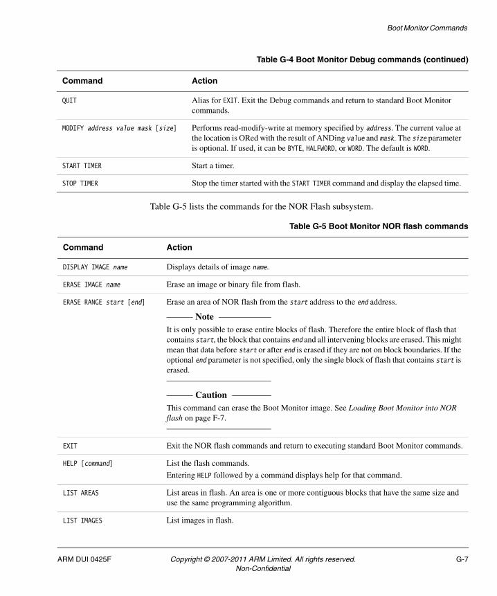
Boot Monitor Commands
Table G-5 lists the commands for the NOR Flash subsystem.
QUIT Alias for EXIT. Exit the Debug commands and return to standard Boot Monitor commands.
MODIFY address value mask [size] Performs read-modify-write at memory specified by address. The current value at the location is ORed with the result of ANDing value and mask. The size parameter is optional. If used, it can be BYTE, HALFWORD, or WORD. The default is WORD.
START TIMER Start a timer.
STOP TIMER Stop the timer started with the START TIMER command and display the elapsed time.
Table G-4 Boot Monitor Debug commands (continued)
Command Action
Table G-5 Boot Monitor NOR flash commands
Command Action
DISPLAY IMAGE name Displays details of image name.
ERASE IMAGE name Erase an image or binary file from flash.
ERASE RANGE start [end] Erase an area of NOR flash from the start address to the end address.
Note It is only possible to erase entire blocks of flash. Therefore the entire block of flash that contains start, the block that contains end and all intervening blocks are erased. This might mean that data before start or after end is erased if they are not on block boundaries. If the optional end parameter is not specified, only the single block of flash that contains start is erased.
Caution This command can erase the Boot Monitor image. See Loading Boot Monitor into NOR flash on page F-7.
EXIT Exit the NOR flash commands and return to executing standard Boot Monitor commands.
HELP [command] List the flash commands.
Entering HELP followed by a command displays help for that command.
LIST AREAS List areas in flash. An area is one or more contiguous blocks that have the same size and use the same programming algorithm.
LIST IMAGES List images in flash.
ARM DUI 0425F Copyright © 2007-2011 ARM Limited. All rights reserved. G-7Non-Confidential

Boot Monitor Commands
LOAD name Load the image image_name into memory.
QUIT Alias for EXIT. Exit the NOR flash commands and return to standard Boot Monitor commands.
RESERVE SPACE address size Reserve space in NOR flash. This space is not be used by the Boot Monitor. address is the start of the area and size is the size of the reserved area.
RUN name Load the image name from flash and run it.
UNRESERVE SPACE address Free the space starting at address in NOR flash. This space can be used by the Boot Monitor.
WRITE BINARY file [NAME new_name] [FLASH_ADDRESS address] [LOAD_ADDRESS address] [ENTRY_POINT address]
Write a binary file to flash. By default, the image is identified by its file name. Use NAME new_name to specify a name instead of using the default name.
Use FLASH_ADDRESS address to specify where in flash the image is to be located. The optional LOAD_ADDRESS and ENTRY_POINT arguments enable you to specify the load address and the entry point.
If an entry point is not specified, the load address is used as the entry point.
Note Remote file access requires semihosting. Use a debugger connection to provide semihosting.
WRITE IMAGE file [NAME new_name] [FLASH_ADDRESS address]
Write an ELF image file to flash. By default, the image is identified by its file name. For example, t:\images\boot_monitor.axf is identified as boot_monitor. Use NAME new_name to specify a name instead of using the default name.
Use FLASH_ADDRESS address to specify where in flash the image is to be located. If the image is linked to run from flash, the link address is used and address is ignored.
Note Remote file access requires semihosting. Use a debugger connection to provide semihosting.
Table G-5 Boot Monitor NOR flash commands (continued)
Command Action
G-8 Copyright © 2007-2011 ARM Limited. All rights reserved. ARM DUI 0425FNon-Confidential

Appendix H Loading FPGA Images
This section describes the format of the board files and how to use the progcards utilities to load images from the supplied CD into the baseboard and Logic Tile FPGAs and PLDs. It contains the following sections:
• General procedure on page H-2
• Board files on page H-3
• The progcards utilities on page H-5
• Upgrading your hardware on page H-6.
ARM DUI 0425F Copyright © 2007-2011 ARM Limited. All rights reserved. H-1Non-Confidential

Loading FPGA Images
H.1 General procedure
The general procedure to load an image is:
1. Follow the instructions in the Versatile CD Installation Guide to install the software and data files on your hard disk.
2. Set up the baseboard and Logic Tile as described in Setting up the PB1176JZF-S on page 2-2.
3. Connect RealView ICE to the JTAG connector or use a USB cable to connect a PC to the USB Config port as described in Connecting JTAG, Trace, and configuration equipment on page 2-10.
4. Place the baseboard in configuration mode (FPGA Config switch ON) and power on the development system.
5. Run progcards and select the configuration that matches your board setup. See Board files on page H-3.
6. Run the progcards utility and load the image files into the FPGAs. See Upgrading your hardware on page H-6). The board file selects the image files to load. Board files have a.brd extension.
Caution You are advised not to reprogram these devices with any images other than those
provided by ARM Limited.
7. After loading new images, set the FPGA images switches to select the appropriate image. See Chapter 2 Getting Started.
H-2 Copyright © 2007-2011 ARM Limited. All rights reserved. ARM DUI 0425FNon-Confidential

Loading FPGA Images
H.2 Board files
The CD includes both the progcards programming utilities and the images to load into the FPGAs and PLDs. See the Application Notes on the CD for the combination of baseboard and Logic Tile that you are using.
H.2.1 Naming conventions for board files
The file name of a board file identifies the PCB, Logic Tile, all programmable devices, and revision. Using the board file eliminates the requirement to load several individual image files. All file names are in lower case with an underscore character separating the fields:
appnote_boardname_number_core_endian_build_devicelist.brd
where:
appnote The Application Note related to this board file.
boardname_number The name and number identify a specific development board. For example, eb_140c is for the baseboard that uses PCB board HBI-140C.
Note The full board number is HBI-XXXXR, this is abbreviated to the
significant digits and revision, for example, HBI-0140C becomes 140C.
core The name of the core that is used with this configuration. For example, mpcore_li identifies the ARM11 MPCore operating in little-endian mode.
Caution Ensure that you use the board file that matches your system
configuration.
buildn The build number. The number n increments from 0
devicelist The name of the programmable devices that are specified in this file.
ARM DUI 0425F Copyright © 2007-2011 ARM Limited. All rights reserved. H-3Non-Confidential
Loading FPGA Images
H.2.2 Naming conventions for image files
The image files contain the image for a single FPGA, PLD, or programmable memory device. The file name of an FPGA or PLD image file identifies the PCB, device and revision. All file names are in lower case with an underscore character separating the fields:
boardname_number_devicename_device_buildn.extension
where:
boardname_number The name and number identify a specific development board. For example, eb_140c is for the baseboard that uses PCB board HBI-140C.
devicename_device
The name of the programmable devices that match this file. For example, cfg_xc2c128 identifies the Xilinx XC2C128 configuration PLD.
buildn The build number. The number n increments from 0
extension The type of device used by this file. For example .svf is used for PLD programming and .bit is used for FPGA programming.
Caution The baseboard is supplied with the PLD images already programmed. The information in this section is provided, however, in case of accidental erasure of the PLDs.You are advised not to reprogram the PLDs with any images other than those provided by ARM Limited.
Using the board file to control image file loading minimizes the risk of incorrectly programming the board. The board files contains a list of correct image files and eliminates the requirement to select individual image files for the programmable devices on the baseboard or attached Logic Tile.
H-4 Copyright © 2007-2011 ARM Limited. All rights reserved. ARM DUI 0425FNon-Confidential

Loading FPGA Images
H.3 The progcards utilities
The progcards utilities are the primary method for programming FPGAs, configuration flash memory, and non-volatile PLDs. These utilities are used during board manufacture and to carry out field upgrades.
progcards reads a description of the board JTAG scan chain and a list of operations from a board description (*.brd) file. The file describes which bitstream and configuration files (*.bit, *.svf) must be downloaded to devices on the board.
The upgrade package for a board contains the new files and all previously released versions. This enables you to return to the original configuration.
Example H-1 Board file
[General]Name = Emulation Board HPI-0140 B build 7 MPCore build working interruptsPriority = 1Board = Emulation_Board[ScanChain]TAPs = 3TAP0 = XC2V6000TAP1 = XC2C128TAP2 = XC2C128[Program]SequenceLength = 4Step1File = an151_eb_140b_cfg_xc2c128_build1.svfStep1Method = PLDStep1Tap = 1Step2Method = Virtex2Step2Tap = 0Step2File = an151_eb_140b_xc2v6000_via_build1.bitStep3Method = IntelFlashStep3Tap = 0Step3Address = 400000Step3File = an151_eb_140b_ctmpcore_li_build7.bitStep4File = an151_eb_140b_mux_xc2c128_build1.svfStep4Method = PLDStep4Tap = 2
ARM DUI 0425F Copyright © 2007-2011 ARM Limited. All rights reserved. H-5Non-Confidential

Loading FPGA Images
H.4 Upgrading your hardware
Use one of the progcards utilities and the board description (*.brd) files to load configuration images to the FPGA:
progcards_rvi.exe
progcards_rvi.exe uses RealView ICE and the JTAG interface. It runs on a PC host in a DOS window and communicates with the RealView ICE interface box.
See Procedure for progcards_rvi.exe for detailed instructions.
progcards_usb.exe
progcards_usb.exe uses the built-in USB Config port (USB to JTAG interface logic) on the baseboard. A standard USB cable connects the baseboard to the PC running progcards_usb.exe.
See Procedure for progcards_usb.exe on page H-8 for detailed instructions.
Note The latest version of the RVI firmware can be downloaded from the Technical Support area of the ARM web site.
H.4.1 Procedure for progcards_rvi.exe
1. Ensure that the RealView ICE firmware is version 1.4.1 (or later) and has the additional patch required for running progcards_rvi. The patch can be downloaded from the downloads page on the Technical Support section of the ARM web site. See the readme file supplied with progcards_rvi for information on updating the firmware.
2. Connect the 20-way JTAG cable from the RealView ICE JTAG interface to the JTAG connector on the rear panel of the micro ATX enclosure. See About the PB1176JZF-S on page 1-2.
3. Set the CONFIG switch to ON.
4. Turn on the power, the orange Config indicator D6.
5. Start a command window by selecting Run from the Start menu and entering command in the text box.
6. Change directory to the directory that contains board description (*.brd) files for the design to be programmed.
H-6 Copyright © 2007-2011 ARM Limited. All rights reserved. ARM DUI 0425FNon-Confidential

Loading FPGA Images
7. Start the programming utility by entering progcards_rvi at the command prompt.
8. A menu is displayed asking which interface box you want to connect to. Select the interface that connects to the baseboard.
Note See the documentation supplied with progcards_rvi for information on
connecting directly to a specified interface that connects to either the network or the local USB connection on the PC.
9. RVI attempts to autoconfigure. If auto-configuration fails, see the documentation supplied with procards_rvi.
10. progcards_rvi searches for board description files that match the JTAG scan chain. All board descriptions matching the first part of the chain are presented as a menu and you can select the file to use.
progcards_rvi runs through the steps required to completely reprogram the boards.
11. To bypass programming a Logic Tile or the baseboard select the Skip option from the menu. progcards_rvi then looks for board description files that match the next segment of scan chain and then the next segment until the procedure is completed.
Typically one menu is displayed for the Logic Tile and one menu is displayed for the baseboard. If only one board description matches your hardware, it is automatically selected and no menu is displayed.
Caution Ensure that the image file you are loading matches your system configuration. If
the incorrect files are loaded, the baseboard and tiles might not function or might be unreliable.
12. After downloading the image completes, turn the power off and move the Config switch.
13. Set the configuration switches to match the boot option you are using. See Setting the configuration switches on page 2-3).
14. Power on and use the Boot Monitor to load your application. See Appendix F Boot Monitor and platform library.
If you are not using the Boot Monitor, use a JTAG debugger to load and run an application. See the documentation supplied with your debugger for details.
ARM DUI 0425F Copyright © 2007-2011 ARM Limited. All rights reserved. H-7Non-Confidential

Loading FPGA Images
H.4.2 Procedure for progcards_usb.exe
1. If it is not already installed, install the USB Config Direct Control software.
Note Windows USB Config drivers must be installed before using the progcards_usb
utility. Information on installing the USB drivers can be found in \boardfiles\USB_Config_driver\readme.txt.
2. Connect the USB cable from the host PC to the USB Config port on the front panel of the micro ATX enclosure. See About the PB1176JZF-S on page 1-2.
3. Set the CONFIG switch to ON.
4. Turn on the power. The orange Config LED lights.
5. Start a command window by selecting Run from the start menu and entering command in the text box.
6. Change directory to the directory that contains board description (*.brd) files for the design to be programmed.
7. Start the programming utility by entering progcards_usb at the command prompt.
Note If progcards_usb.exe is not in the current working directory, set your PATH
environment variable to point to the directory that contains progcards_usb.exe.
8. Progcards_usb searches for board description files that match the scan chain. All board descriptions matching the first part of the chain are presented as a menu and you can select the file to use.
progcards_usb runs through the steps required to completely reprogram the boards.
9. To bypass programming a Logic Tile or the baseboard select the Skip option from the menu. progcards_usb then looks for board description files that match the next segment of scan chain and then the next until the process is completed.
Typically one menu is displayed for the Logic Tile and one menu is displayed for the baseboard. If only one board description matches your hardware, it is automatically selected and no menu is displayed.
10. After downloading the image completes, turn the power off and move the Config switch to the OFF position.
H-8 Copyright © 2007-2011 ARM Limited. All rights reserved. ARM DUI 0425FNon-Confidential

Loading FPGA Images
11. Set the configuration switches to match the boot option you are using. See Setting the configuration switches on page 2-3.
12. Power on the board and use the Boot Monitor to load your application. See Appendix F Boot Monitor and platform library.
If you are not using the Boot Monitor, use a JTAG debugger to load and run an application. See the documentation supplied with your debugger for details.
H.4.3 Troubleshooting
If the upgrade process fails at any time, or the progcards utility reports an error, then check the following:
1. The Config switch is ON and the orange Config LED is on.
2. If you are using progcards_rvi.exe, see the documentation supplied with progcards_rvi.
3. If you are using progcards_usb.exe ensure that:
a. the USB cable is plugged into the USB Config port.
b. the USB Config drivers are installed on your machine.
4. Ensure that any Logic Tiles are correctly stacked on the baseboard. If necessary, push them firmly to ensure a proper connection.
5. Look for any readme.txt files that might be present in the directory that contains the board description (*.brd) files. Follow the instructions provided for new or updated software or engineering changes.
Caution The 1.5V cell battery provides the VBATT backup voltage to the external DS1338 time-of-year clock and FPGA encryption key circuitry within the FPGA. Removing the battery erases the encryption key.
See FPGA configuration on page 3-30 for details safely replacing the battery.
ARM DUI 0425F Copyright © 2007-2011 ARM Limited. All rights reserved. H-9Non-Confidential

Loading FPGA Images
H-10 Copyright © 2007-2011 ARM Limited. All rights reserved. ARM DUI 0425FNon-Confidential
Glossary
This glossary lists abbreviations used in this guide.
ADC Analog to Digital Converter. A device that converts an analog signal into digital data.
AACI Advanced Audio CODEC Interface.
AHB Advanced High-performance Bus. The ARM open standard for on-chip buses.
AMBA Advanced Microcontroller Bus Architecture.
APB Advanced Peripheral Bus. The ARM open standard for peripheral buses. This design is optimized for low power and minimal interface complexity.
APC Advanced Power Controller. National Semiconductor device used to monitor and control power. This is used by the IEM subsystem.
AXD ARM eXtended Debugger.
AXI Advanced eXtensible Interface. The ARM open standard for high-performance and high-frequency buses.
BOM Bill Of Materials. A list of all the parts used on the printed circuit board and any specific build instructions for board variants.
ARM DUI 0425F Copyright © 2007-2011 ARM Limited. All rights reserved. Glossary-1Non-Confidential

Glossary
CLCD Color Liquid-Crystal Display.
CODEC COder DECoder for converting between analog and digital audio signals.
DAC Digital to Analog Converter. A device that converts digital data into analog level signals.
DCC Debug Communications Channel.
DDR Double Data Rate, DRAM with high-speed data access.
DOC Disk-On-Chip. A non-volatile flash memory device with an interface that simplifies file accesses. Also called NAND flash referring to the logic gates used internally. The memory can only be accessed sequentially in blocks.
DMC Dynamic Memory Controller.
DRAM Dynamic Random Access Memory.
DSR Data Set Ready, a UART flow-control signal.
DTR Data Terminal Ready, a UART flow-control signal.
ETB Embedded Trace Buffer.
ETM Embedded Trace Macrocell.
FET Field Effect Transistor.
FPGA Field Programmable Gate Array.
GIC Generic Interrupt Controller.
GPIO General Purpose Input/Output.
GTC Generic Test Chip. A packaging and signal assignment specification for test chips.
ICE In Circuit Emulator. A interface device for configuring and debugging processor cores.
IEM Intelligent Energy Management. A system for monitoring and controlling chip voltages and frequencies to reduce power consumption.
I/O Input/Output.
IP Intellectual Property.
JTAG Joint Test Action Group. The committee which defined the IEEE test access port and boundary-scan standard.
KMI Keyboard/Mouse Interface.
LCD Liquid Crystal Display.
Glossary-2 Copyright © 2007-2011 ARM Limited. All rights reserved. ARM DUI 0425FNon-Confidential
Glossary
LED Light Emitting Diode.
MAC Media Access Control. A layer in the Ethernet specification.
MCI MultiMedia Card Interface.
MMC MultiMedia Card.
Multi-ICE Multi-ICE is a system for debugging embedded processor cores using a JTAG interface. See ICE.
NAND flash Non-volatile memory. NAND refers to the type of logic gate used internally. See DOC.
NOR flash Non-volatile memory. NOR refers to the type of logic gate used internally. Any memory address can be accessed randomly.
OTG On-The-Go, a USB specification.
PCB Printed Circuit Board.
PCI Peripheral Component Interconnect. A computer bus for attaching peripherals.
PHY PHYsical layer. The layer in the Ethernet specification that describes the physical interface.
PISMO Platform Independent Storage Module. Memory specification for plug in memory modules.
PLD Programmable Logic Device.
PLL Phase-Locked Loop, a type of programmable oscillator.
POR Power On Reset.
RAM Random Access Memory.
RVI RealView ICE. A system for debugging embedded processor cores using a JTAG interface. See also ICE.
RTC Real-Time Clock.
RVD RealView Debugger.
SRAM Static Random Access Memory.
SBZ Should be Zero. Indicates that the bit in the register is reserved and must be set to zero.
SCI Smart Card Interface.
SD Secure Digital memory card specification.
SMC Static Memory Controller.
ARM DUI 0425F Copyright © 2007-2011 ARM Limited. All rights reserved. Glossary-3Non-Confidential

Glossary
SMM Soft Macrocell Model of a CPU core.
SSP Synchronous Serial Port.
TCM Tightly Coupled Memory. Memory present inside the test chip that typically runs at or near the processor speed.
TPA Trace Port Analyzer.
TrustZone ARM TrustZone technology is a key enabling technology for securing consumer products such as mobile phones, PDAs, set top boxes or other systems running open Operating Systems.
UART Universal Asynchronous Receiver/Transmitter.
USB Universal Serial Bus.
VGA Video Graphics Array.
Glossary-4 Copyright © 2007-2011 ARM Limited. All rights reserved. ARM DUI 0425FNon-Confidential