recent activities of the actinic inspection using the euv ... · recent activities of the actinic...
TRANSCRIPT

Recent Activities of the Actinic Mask Inspection using the EUV microscope at Center for EUVL
Takeo Watanabe, Tetsuo Harada, and Hiroo Kinoshita
Center for EUVL, University of Hyogo

Outline
1) EUV actinic mask inspection using EUV Microscope
2) EUV Microscope using a high‐magnification objective with three multilayer mirrors

EUV actinic mask inspection using EUV Microscope
Takeo Watanabe, Tetsuo Harada, Hiroo Kinoshita,Center for EUVL, LASTI, University of Hyogo
Tsuyoshi Amano, Osamu Suga, Selete** Present affiliation: EIDEC

Outline
1) EUV microscope2) Phase defect observation3) Defect repairing using FIB and its
observation4) Conclusions

5
Background
Total 11 sets of the commercial steppers for EUV Lithographywill be delivered in 2013 ~ 2014.
EUV mask repairand
the mask inspection for the repaired maskis required
Mask pattern defect Electric circuit error Device error

New SUBARU SRBeamLine 3
X線ズーミング管(10~200X)
Schwarzschild光学系(NA0.3 倍率30X)
ロードロック サンプル
CCD
除振台
New SUBARU SRBeamLine 3
X線ズーミング管(10~200X)
Schwarzschild光学系(NA0.3 倍率30X)
ロードロック サンプル
CCD
除振台
Glass
Amplitude defect Phase defect
Affected with Intensity profile
Affected withthe phaseprofile
(pit defect)
Glass
EUV Mask Defect
Inspection by exposure wavelength
Pit and bump defects of 1‐nm‐depth are printable.
Mask inspection method
EUV mask defect inspection tool
ALSZone Plate型
NewSUBARUSchwarzschild型
hp100 nm
hp150 nm
Difficult to inspect using DUV and SEM.
EUV顕微鏡

Specification of EUV Microscope
Schwarzschild optics(Multilayer mirror, NA 0.3, 30X)
New SUBARU SRBeamLine 3
Load-lock chamber
Vibration isolator
front-end turning mirror(Multilayer mirror)
back-end turning mirror(Multilayer mirror)
(c) CCD camera
X-Y-Z sample stage
X-ray zooming tube(10~200X)Schwarzschild optics
Magnification : 30XNumerical aperture: 0.3
・Light source Bending magnet・Total magnification 300~6000x・Resolution 10 nm・Method Bright field・Defect observation Amplitude and phase defects

Mask defect inspection by EUVM
Dark area
150nm L/S
Amplitude Phase
Mo/Si ML
ULE Substrate
Absorber
500nm 3um
600X
Contamination 1um Dot
Finished mask Blanks

0
2000
4000
6000
8000
10000
12000
0 20 40 60 80 100 120 140
50 nm
pixels
Inte
nsity
(arb
. uni
ts)
0
2000
4000
6000
8000
10000
12000
0 20 40 60 80 100 120 140
50 nm50 nm
pixels
Inte
nsity
(arb
. uni
ts)
By 25% and 75% of maximum light intensity light for the absorber edge pattern, the resolution of 50nm is obtained.
Isolated line of 300 nm width
Resolution of mask defect by EUVM
1200X
Pattern edge profile of lightintenisty

Printability of phase defect under the absorber pattern
400 nm L/S,programmed defect height of 12 nm
Printability of Mask Defect
0
1
2
3
4
5
0 10 20 30 40 50 60 70 80 90 100 110 120 130 140 150
Printable area
Non-printable area
Width (nm)
Dep
th (n
m)
Line-pit defects Resolved Not resolved
Line-pit defects Resolved Not resolved
Hole-pit defects Resolved Not resolved
Hole-pit defects Resolved Not resolved
Printability of point and line programmed defects
Controlled the width and height of the programmed defect.
Depth: 1~4 nmWidth: 20~140 nmThe printability criteria was clarified using EUVM.
The printability depends on the position of the programmed defect.
Printability
Hp 400 nm

11
Repair of clear defect
Resist image
Lack of circuit pattern
EUVM image
Clear defect
Clear defect(Reflected region)
ML
SEM image
Lack of absorberAbsorber

Conventional repairing method of clear defect by CVD
Demerrit:• CVD layer contains carbon.
Thickness loss by cleaning.• CVD layer has to be large height.
Affected with shadowing effect

Abs.
ML
Mask defect repair using FIB
By removing of the ML under the Clear defect by the Ga ion beam of FIB, the EUV light will not be reflected.

14
Pattern inspection by EUVM for the repaired clear defect by FIB
225 nm L/S
500nm
ML removal area
FIB irradiation areaNarrow width Wide width
SEM image
EUVM像
Not completely removed Completely removedClear defectNarrow width for repairing

128 nm L/SFIB irradiation area
The clear defect which was repaired by FIB was observed using EUVM.
EUVM image
500 nm
Pattern inspection by EUVM for the repaired clear defect by FIB
Narrow width Wide width

1) Printability criteria of the programmed defect width and height was obtained using EUVM mask defect inspection.
2) It is confirmed that the clear defect repairing by FIB is found to be usable using the EUVM observation.
Conclusions

Acknowledgement
This research was supported by NEDO.
And the mask sample was prepared by Selete.
EUV Microscope using a high‐magnification objective with three multilayer mirrors
M. Toyoda, K. Yamasoe, T. Hatano, M. YanagiharaLab. of Soft X-ray microscopy, IMRAM, Tohoku University
A. Tokimasa, T. Harada, T. Watanabe, H. KinoshitaLASTI, University of Hyogo

Outline
1. MotivationEarly studies and technical issues
2. ExperimentalInnovative optics utilizing high‐magnification
3. Highlight dataEUVL mask images with improved resolution
4. Summary and future plans

1. Motivation

Benefit of using high-magnification mirror as an objective
In the x-ray zooming tube, CsI thin film was utilizedas the photoelectric conversion element.
However, the grain size of the CsI affected with the resolution of the EUVM imaging.
Thus the high-magnification-mirror objective is selected for the EUVM imaging.

At‐wavelength inspection of EUVL mask
absorber
defects
Mo/Sisubstrate
<100nm
Requirements for an inspection toolAt‐wavelength observation (λ=13.5nm)High spatial resolution (δ<40nm)Wide field of view for a rapid whole mask inspection
defects

SR EUV light EUV zooming tube(200x)
Schwarzschildobjective(30x)NA=0.3
EUV⇒electronBright field image at λ=13.5 nmRayleigh’s limit δ=30 nmField of view Φ=20μmActual resolution δ>100 nm
H. Kinoshita Jpn. J. Appl. Phys. 49(2010)06GD07.
Line width 480nm(120nm on wafer)
mask sample
Early study: EUV Microscope on NewSUBARU
electron lens
photo cathode

Aim of this work
Degraded resolution resulting from aberrations of Schwarzschild objective.
Small field of viewlimited by an electron lens of the zooming tube.
Innovative EUV imaging facility realizing bothhigh spatial resolution for 22-nm node mask,wider field of view for practical inspection time.
Technical issues of the EUV Microscope
2. Experimental
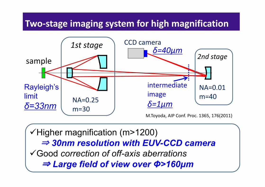
1st stage
sample
NA=0.25m=30
Rayleigh’slimitδ=33nm
M.Toyoda, AIP Conf. Proc. 1365, 176(2011)
Two‐stage imaging system for high magnification
2nd stage
NA=0.01m=40
CCD camera
intermediateimageδ=1μm
δ=40μm
Higher magnification (m>1200)⇒ 30nm resolution with EUV-CCD camera
Good correction of off-axis aberrations⇒ Large field of view over Φ>160μm

NewSUBARU BL3
Schwarzschildobjective
CCD camera
EUVL mask
turning mirror
intermediateimage
load‐lock system
600mm
Experimental setup of the novel facility
Schwarzschildobjective
illumination optics 2nd stagemirror
2nd stagemirrorSR EUV

9.3nm‐5.5nm
Instrumentation of the imaging optics
Concave mirror
Convex mirror50mm
Substrates (5 sets) were polished in IMRAM.Mo/Si multilayer was coated with IBS.Mirrors were aligned using Zygo interferometer.⇒ Wavefront error W=2.2 nm rms. (on-axis)

3. Highlight data

Intermediate image (m=30)
EUV‐CCD camera: pixel size 13.5μm, 2048×2048 pixels
5μm
50μm
Exp. time: 0.25 sec. Line width: 240nm (60nm)Exp. time: 36 sec.
Confirmation of the magnification enhancement
Final image (m=1460)

5μm
Line width: 225nm (56nm)Exp. time: 10s
Resolution measurement with L/S patterns High magnification images (m=1460)
Line width: 88nm (22nm)Exp. time:100s
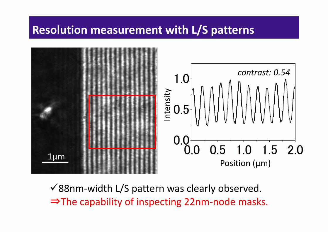
5μm
88nm‐width L/S pattern was clearly observed.⇒The capability of inspecting 22nm‐node masks.
Intensity
contrast: 0.54
Position (μm)1μm
Resolution measurement with L/S patterns

1) High‐magnification of 1460x was achieved using three‐mirror objective.
2) High‐magnification enhancement was confirmed by the observation of the actinic EUV mask.
3) 88 nm mask pattern was observed using high‐magnification objective in EUVM.
Conclusions

1) Printability criteria of the programmed defect was confirmed by EUVM.
2) The benefit of the clear defect repairing method using FIB was confirmed by EUVM.
3) 88 nm mask pattern was observed using high‐magnification objective in EUVM.
Summaries