recent advances in rebco coated conductors via …sang...electronic materials & devices...
TRANSCRIPT

Electronic Materials & Devices LaboratorySeoul National UniversityDepartment of Material Science & Engineering
Recent Advances in REBCO Coated Conductors
via the RCE-DR process
Sang-Im Yoo
Department of Materials Science & Engineering & Research Institute
of Advanced materials (RIAM), Seoul National University,
Seoul 151-744, Korea
ALCA-JST International Workshop Mar. 7-9, 2016 @ Osaka, Japan

Seoul National UniversityDepartment of Material Science & EngineeringElectronic Materials & Devices Laboratory
CollaboratorsGraduate Students in SNU (Seoul National University)
Dr. Jung-Woo Lee
(postdoc @ Univ. of Wisconsin)
Dr. Soon-Mi Choi
(Samsung Display Co.)
Mr. Tae-Hyun Seok
(SK Hynix)
Mr. Won-jae Oh
Dr. Hunju Lee
Researchers in SuNAM (Superconductor, Nano & Advanced Materials) Co.
Dr. Jae-Hun LeeDr. Seung-Hyun Moon
(CEO)
Researchers in KERI (Korea Electrotechnology Research Institute)
Dr. Hong-Soo Ha Dr. Sang-Soo Oh
New Graduate Students:Mr. In-Sung ParkMr. Jae-Eun KimMr. Duho Lee
Electronic Materials & Devices Laboratory Seoul National UniversityDepartment of Materials Science & Engineering
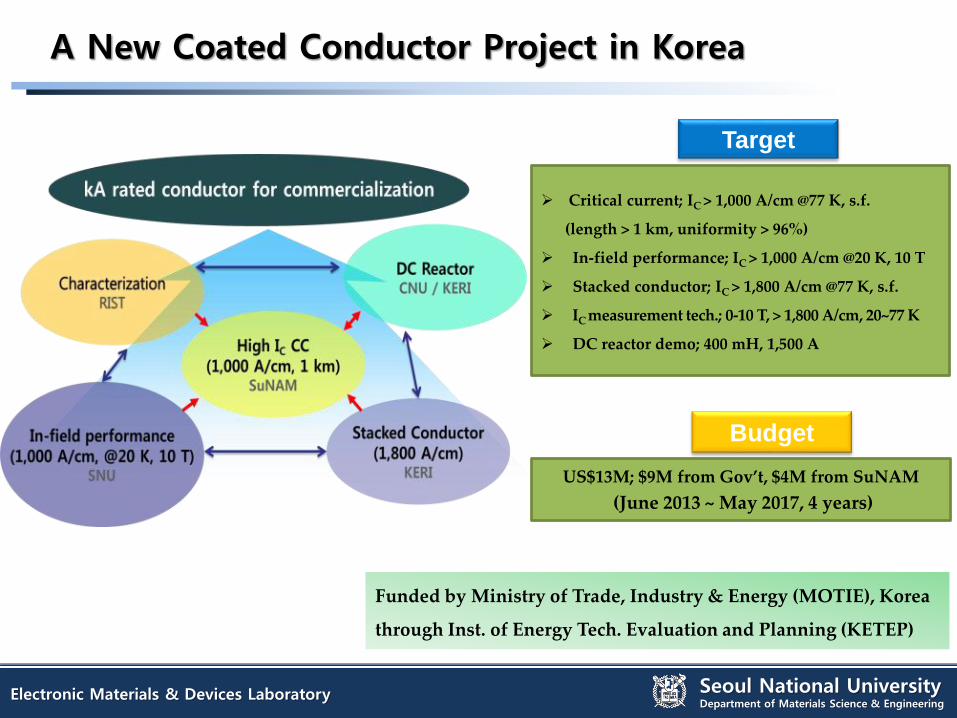
A New Coated Conductor Project in Korea
Funded by Ministry of Trade, Industry & Energy (MOTIE), Korea
through Inst. of Energy Tech. Evaluation and Planning (KETEP)
Critical current; IC > 1,000 A/cm @77 K, s.f.
(length > 1 km, uniformity > 96%)
In-field performance; IC > 1,000 A/cm @20 K, 10 T
Stacked conductor; IC > 1,800 A/cm @77 K, s.f.
IC measurement tech.; 0-10 T, > 1,800 A/cm, 20~77 K
DC reactor demo; 400 mH, 1,500 A
US$13M; $9M from Gov’t, $4M from SuNAM
(June 2013 ~ May 2017, 4 years)
Target
Budget
Seoul National UniversityDepartment of Material Science & EngineeringElectronic Materials & Devices Laboratory
Outline
I. Introduction
SuNAM : Superconductor, Nano & Advanced Materials (瑞藍)
RCE-DR (Reactive Co-Evaporation Deposition & Reaction)
II. Recent Advances in REBCO CC
Optimization of conversion processing from an amorphous precursor to
REBCO film on the basis of phase stability diagrams in low PO2
Pinning improvement in GdBCO CCs by the RCE-DR process
III. Summary

Seoul National UniversityDepartment of Material Science & EngineeringElectronic Materials & Devices Laboratory
Production Facilities of SuNAM Co.
Site area : 5,500 m2,
Building area : 1,750 m2,
Gross floor area : 3,050 m2.
Class < 10,000 clean
room area : 1,000 m2 .
Production capacity ~ 60 km/month(4 mm width) considering the yield(~ 70 %)
Introduction

Seoul National UniversityDepartment of Material Science & EngineeringElectronic Materials & Devices Laboratory
Hastelloy C276 (Ni-alloy tape)
or
SUS-tape
Seed layer (Y2O
3)
~ 7 nm
IBAD-MgO layer ~ 10 nm
Homoepi-MgO layer ~ 20 nm
Diffusion barrier (Al2O3)
~ 40 nm
Hastelloy
or SUS
Al2O3
Y2O3
IBAD-MgO
Epi-MgO
LaMnO3
REBCO
Ag
Buffer layer ~20 nm
Superconducting layer (1 ~ 3 μm)
Protecting layer (1.5 mm)
IBAD(Sputter & E-beam)
Sputter
RCE-DR
DC sputter
Electro-polishing
( + Cu electroplating (+ lamination))
SuNAM HTS 2G Wire ArchitectureIntroduction

Electronic Materials & Devices Laboratory Seoul National UniversityDepartment of Materials Science & Engineering
<Schematic of the RCE-DR process>
High rate deposition at low temperature & low oxygen pressure to a target thickness
(> 1 μm) at once in the deposition zone (6 ~ 10 nm/s)
Fast conversion by RCE-DR from an amorphous phase to superconductor at high
temperature and relatively higher oxygen pressure in the reaction zone
Simple, low system cost, easy to scale up (high deposition rate & large deposition area)
MOCVD (Superpower) : ~ 180 m/h 1)
PLD (Fujikura) : 20 m/h 2)
MOD (AMSC) : ~ 100 m/h 3)
RCE-DR (SuNAM) > 360 m/h 4)
1) 2008 DOE Superconductivity Peer Review, Superpower, Inc.
2) 2009 “RE123 Coated Conductors”, Fujikura Annual reports
3) 2009 DOE Superconductivity Peer Review, AMSC Co.
4) 2010 ISS S.H. Moon (SuNAM) invited talk,
2011 MRS spring meeting S.I. Yoo (SNU) invited talk
<Throughput of each processing
method – 4mm width equivalent >
RCE-DR : Reactive Co-Evaporation Deposition & Reaction
Introduction
RCE DR : ~ 100 nm/sec or faster (SuNAM)
PLD, MOCVD ~ 10 nm/sec, MOD ~ 1 nm/sec

Seoul National UniversityDepartment of Material Science & EngineeringElectronic Materials & Devices Laboratory
IntroductionRecent report from SuNAM
J.H. Lee et al., Supercond. Sci. Technol. 27 (2014) 044018
Seoul National UniversityDepartment of Material Science & EngineeringElectronic Materials & Devices Laboratory
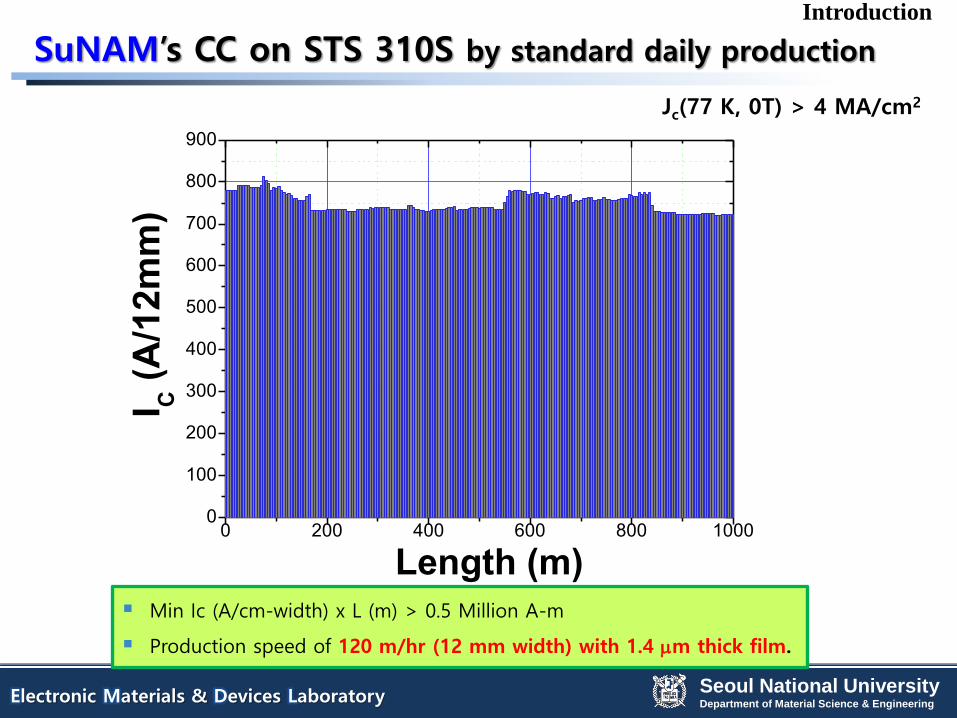
SuNAM’s CC on STS 310S by standard daily production
Introduction
0 200 400 600 800 10000
100
200
300
400
500
600
700
800
900
Length (m)
I C (
A/1
2m
m)
Jc(77 K, 0T) > 4 MA/cm2
Min Ic (A/cm-width) x L (m) > 0.5 Million A-m
Production speed of 120 m/hr (12 mm width) with 1.4 mm thick film.
Introduction

[ Specification Table ]
Model AN CN LB/LS K
DescriptionSilver(+Cu…)Dry coating
CopperWet Coating
Brass/ Stainless steelLamination
Polyimide tape(+)Insulation
Substrate Hastelloy or Non-magnetic Stainless Steel
Width[ mm ]
Commercial : 4 mm, 12 mm.Special Order : 2 ~ 10 mm multi width is available
Thickness[ mm ]
HAS : 0.06~0.07SS* : 0.11~0.12
HAS : 0.09~0.11SS* : 0.14~0.16
HAS : 0.18~0.22SS* : 0.23~0.27
+ 0.1
FinalProcess
SilverSputter
CopperPlating
Brass or SS*Lamination
Wrapping
PieceLength
Above 100 m , 200 m , 300 m + without Splice
Min. Ic@ 77 k S.F.
(100 ) / 150 / 200 A + @ 4 mm (300 / 400) / 500 / 600 / 700 A + @ 12 mm
SuNAM’s 2G HTS Wire
(From Dr. Moon, CEO of SuNAM)

0 100 200 300 400 500 600 700 800 900 1000 11000
100
200
300
400
500
600
700
800
900
1000
Ic (
A/c
m-w
) @
77 K
Length (m)
●
10kAm
100kAm
200kAm
300kAm
Ic x L :
400kAm
500kAm
600kAm
700kAm
●
Development of HTS 2G Wire
(2009.8)
1065mx282A
(2008.10)
500mx300A
(2006.7)
100mx253A
(2010.10)
540mx466A
(2011.2)
816mx572A
(2014.03)
978mx579A
(2013.12)
860mx600A
2017 Goal
(2014.02)
270mx370A
(2016 Target)
500mx400A
(2014.11)
997mx601A
Introduction

Seoul National UniversityDepartment of Material Science & EngineeringElectronic Materials & Devices Laboratory
Optimization of conversion processing from an amorphous
precursor to REBCO film on the basis of phase stability
diagrams in low PO2
Pinning improvement in GdBCO CCs by the RCE-DR process
II. Recent Advances in REBCO CC via RCE-DR

Seoul National UniversityDepartment of Material Science & EngineeringElectronic Materials & Devices Laboratory
Objectives
To achieve higher performance GdBCO CC through the optimization of
RCE-DR processing
Development of a new pinning site applicable to the RCE-DR process
Motivation
A routine RCE-DR process of SuNAM should be improved for producing
higher performance GdBCO CCs and also developed for other REBCO CCs.
0.5 um1 0 0 n m
S.M. Choi et al., IEEE Trans. on Appl. Supercond. 23 (2013) 8001004
Motivation & Objectives
Seoul National UniversityDepartment of Material Science & EngineeringElectronic Materials & Devices Laboratory
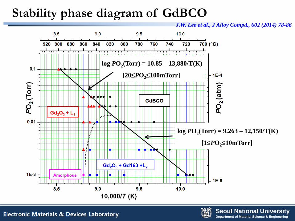
Stability phase diagram of GdBCO
log PO2(Torr) = 10.85 – 13,880/T(K)
[20PO2100mTorr]
log PO2(Torr) = 9.263 – 12,150/T(K)
[1PO210mTorr]
J.W. Lee et al., J Alloy Compd., 602 (2014) 78-86

Seoul National UniversityDepartment of Material Science & EngineeringElectronic Materials & Devices Laboratory
500 nm
Gd
Ba
Cu
O
Cu
Cu
Cu
CuGd
Ba
Cu
O
O
CuCu
Gd
BaO
O
Gd2O3
GdBCO
Cu-O
• Very low PO2 zone (~ 10-5 Torr): Amorphous Film
• Lower PO2 zone (~30 mTorr): Gd2O3 + Liquid (< 5 sec)
• Higher PO2 zone (~100 mTorr): GdBCO Film (< 1min)
GdBCO growth mechanism: a seeded melt-textured growth!!!
Growth mechanism of the GdBCO film by RCE-DR

Seoul National UniversityDepartment of Material Science & EngineeringElectronic Materials & Devices Laboratory
Production rate ≥ 360 m(4 mm width) / h
Control of conversion processing conditions
Processing routes for GdBCO CCs
880ºC 860ºC 840ºC
10000/T (K)
150mTorr
Gd : Ba : Cu ≈ 1 : 1 : 2.5
Precursor composition
Electronic Materials & Devices Laboratory Seoul National UniversityDepartment of Material Science & Engineering
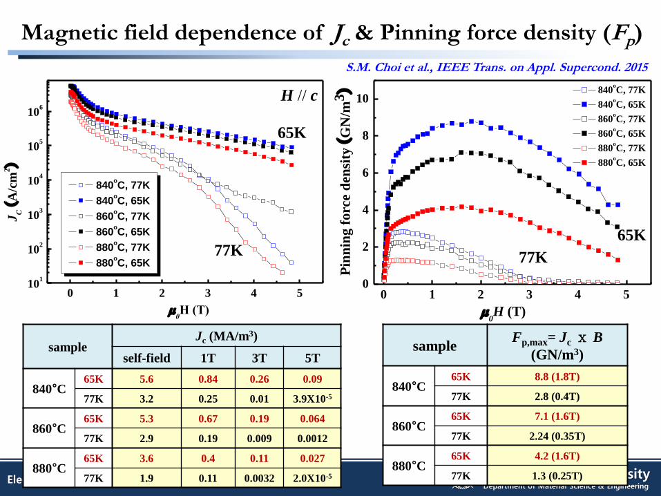
sampleJc (MA/m3)
self-field 1T 3T 5T
840°C65K 5.6 0.84 0.26 0.09
77K 3.2 0.25 0.01 3.9X10⁻⁵
860°C65K 5.3 0.67 0.19 0.064
77K 2.9 0.19 0.009 0.0012
880°C65K 3.6 0.4 0.11 0.027
77K 1.9 0.11 0.0032 2.0X10⁻⁵
0 1 2 3 4 510
1
102
103
104
105
106
840oC, 77K
840oC, 65K
860oC, 77K
860oC, 65K
880oC, 77K
880oC, 65K
77K
65K
JC (
A/c
m2)
m0H (T)
H // c
Magnetic field dependence of Jc & Pinning force density (Fp)
0 1 2 3 4 50
2
4
6
8
10 840
oC, 77K
840oC, 65K
860oC, 77K
860oC, 65K
880oC, 77K
880oC, 65K
77K
65K
Pin
nin
g f
orc
e d
en
sity
(G
N/m
3)
m0H (T)
sampleFp,max= Jc ⅹ B
(GN/m3)
840°C65K 8.8 (1.8T)
77K 2.8 (0.4T)
860°C65K 7.1 (1.6T)
77K 2.24 (0.35T)
880°C65K 4.2 (1.6T)
77K 1.3 (0.25T)
S.M. Choi et al., IEEE Trans. on Appl. Supercond. 2015

Electronic Materials & Devices Laboratory Seoul National UniversityDepartment of Material Science & Engineering
0 30 60 90 120 150 180 210 240
0.2
0.4
0.6
0.8
1.0
1.2
1.4
1.6
1.8
2.0 840
oC
860oC
880oC
H//ab77K, 1T
Angle (deg.)
Jc (
MA
/cm
2)
0 30 60 90 120 150 180 210 2400.0
0.5
1.0
1.5
2.0
2.5
840oC
860oC
880oC
H//ab65K, 3T
Angle (deg.)
Jc (
MA
/cm
2)
Angular dependence of Jc
The GdBCO CCs by RCE-DR show a sharp Jc peak at θ = 90° (H//ab).
A small broad peak of Jc near θ = 180° (H//c) is also observed.
The sample grown at 840°C shows higher Jc values compared with those of samples
grown at higher temperatures.
S.M. Choi et al., IEEE Trans. on Appl. Supercond. 2015

Electronic Materials & Devices Laboratory Seoul National UniversityDepartment of Material Science & Engineering
20 25 30 35 40 45 50 55 60 65 70
(00
8)
(10
3)
Ba
Cu
O2
2 (Cu K)
Gd
2O
3(6
22
)
Gd
2O
3(4
40
)
840oC
(150mTorr)
880oC
(150mTorr)
Gd
2O
3(4
00
)
Gd
2O
3(2
22
) (00
7)(0
06
)
(00
5)
(00
4)
Ni
(11
1)
Ni
(00
2)
Cu
O(2
02
)
Mg
O(2
00
)
Cu
O (
-11
1)
(00
3)
Inte
nsi
ty (
Arb
.un
it)
860oC
(150mTorr)
XRD θ-2θ scans and texture analysis of GdBCO CCs
840 860 880
1
2
32
3
4
5
Temperature (oC)
(
deg
.)(
deg
.)
Δ () Δω ()
840 C 4.28 2.53
860 C 3.37 1.54
880 C 2.6 1.04
The GdBCO (00l) reflections indicate that the GdBCO films are highly c-axis oriented. The
second phases such as Gd2O3 and CuO peaks are also observed in addition to the substrate peaks.
A small GdBCO (103) peak is observed for the film prepared at 840 °C, suggesting that a small
amount of randomly oriented GdBCO grains exist in the film.
S.M. Choi et al., IEEE Trans. on Appl. Supercond. (accepted)

Electronic Materials & Devices Laboratory Seoul National UniversityDepartment of Material Science & Engineering
0 . 2 µ m0 . 2 µ m 0 . 2 µ m
840C 860C 880C
Cross-sectional TEM images
The average particle sizes of Gd2O3 are 126.5 ± 42.6 nm in the 840°C sample, 171.4
± 53.1 nm in the 860°C sample, and 217.8 ± 49.4 nm in the 880°C sample.
S.M. Choi et al., IEEE Trans. on Appl. Supercond. 2015

Electronic Materials & Devices Laboratory Seoul National UniversityDepartment of Material Science & Engineering
20mm 20mm
20mm 20mm 20mm
20mm
840 ºC sample
Polarized light microscope images
S.M. Choi et al., IEEE Trans. on Appl. Supercon. (accepted)

Electronic Materials & Devices Laboratory Seoul National UniversityDepartment of Material Science & Engineering
EBSD analysis data of 840 °C sample
4μm
Image quality map Inverse pole figure image
5μm
Image quality map Inverse pole figure image
S.M. Choi et al., IEEE Trans. on Appl. Supercon. (accepted)

Seoul National UniversityDepartment of Material Science & EngineeringElectronic Materials & Devices Laboratory
For the nominal composition of Gd:Ba:Cu = 1:1:2.5
Decreased intermediate
PO2 zone below 800oC!!!

Seoul National UniversityDepartment of Material Science & EngineeringElectronic Materials & Devices Laboratory
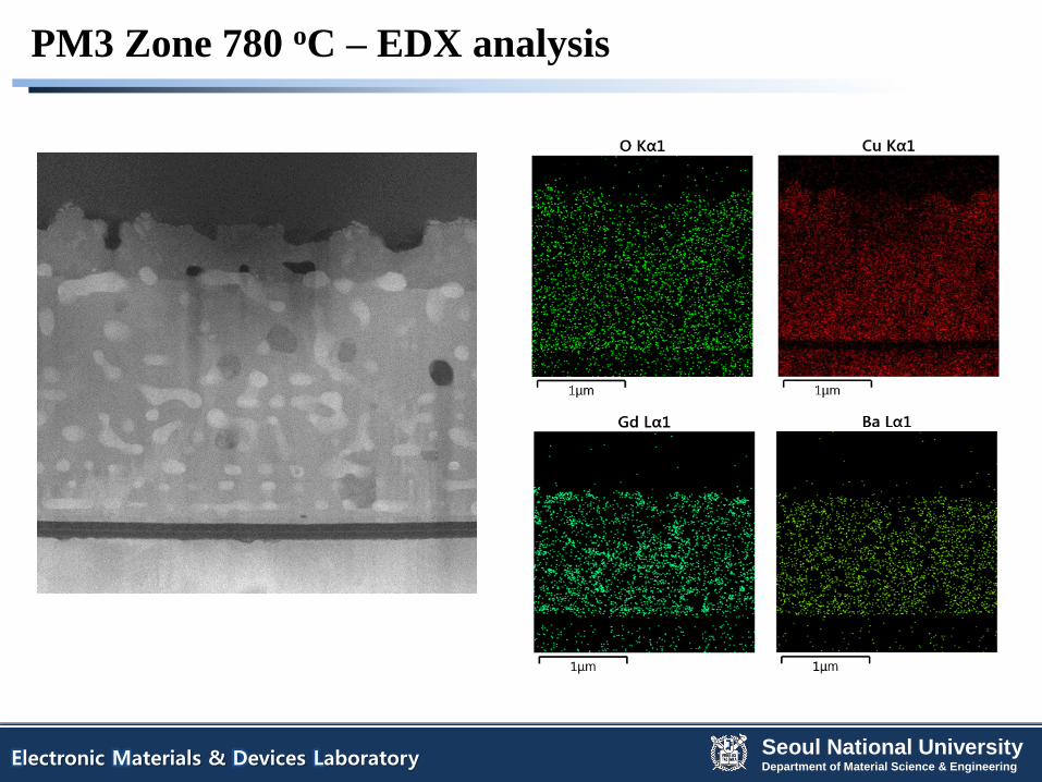
PM3 Zone 780 oC
SEM micrographs of the surface morphology
X 5k X 10k
Normal process

Seoul National UniversityDepartment of Material Science & EngineeringElectronic Materials & Devices Laboratory
PM3 Zone 780 oC – TEM analysis
1 um1 um 0.5 um0.5 um
Particle size (Gd2O3) : 105.1 ± 95.6 nm
Seoul National UniversityDepartment of Material Science & EngineeringElectronic Materials & Devices Laboratory
PM3 Zone 780 oC – EDX analysis

Increased pinning properties by composition control
(1.0 1.4 3.6)
Compositions studied here give a more
Cu-rich liquid which influences growth
kinetics and pinning
There will be Gd2O3 particles in all GdBCO samples but a
specific precursor composition, PO2, and T are key factors
determining their performance. It is clear that very fine Gd2O3
nanoparticles result in the highest performance.
Driscoll et al., AIP Materials 2, 086103 (2014)
(From Dr. Moon, CEO of SuNAM)

In-field Performance (77 K)
(By Dr. Izumi, ISS2012(Japan))
RCE-DR GdBCO w/o APC (C,D composition)
SuNAM’s
present
: 1.4 um
Only with composition control in RCE-
DR process, we can achieve strong
pinnings without APCs.
Driscoll et al., AIP Materials 2, 086103 (2014)
(From Dr. Moon, CEO of SuNAM)

Electronic Materials & Devices Laboratory Seoul National UniversityDepartment of Materials Science & Engineering
Stability phase diagrams of REBCO (RE: Y, Gd, Sm)
(a) T.B. Lindemer et al.,
Physica C 178 (1991)
93-104.
(b) J.L. MacManus-Driscoll et
al., Physica C 241 (1995)
401-413.
(c) K. Iida et al., Supercond.
Sci. Technol. 19 (2006)
S478-S485.
(d) J.W. Lee et al.,
J. Alloys Compd. 602,
(2014) 78-86.
(e) C. Wende et al.,
J. Alloys Compd. 381
(2004) 320–326.
(f) J.H. Song, Master thesis,
Seoul National University
(2014)
Seoul National UniversityDepartment of Material Science & EngineeringElectronic Materials & Devices Laboratory
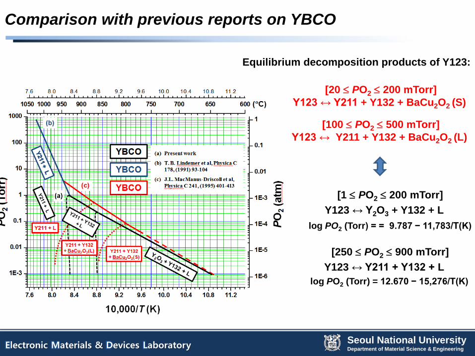
[1 PO2 200 mTorr]
Y123 ↔ Y2O3 + Y132 + L
log PO2 (Torr) = = 9.787 − 11,783/T(K)
[250 PO2 900 mTorr]
Y123 ↔ Y211 + Y132 + L
log PO2 (Torr) = 12.670 − 15,276/T(K)
[20 PO2 200 mTorr]
Y123 ↔ Y211 + Y132 + BaCu2O2 (S)
[100 PO2 500 mTorr]
Y123 ↔ Y211 + Y132 + BaCu2O2 (L)
Equilibrium decomposition products of Y123:
Comparison with previous reports on YBCO

Seoul National UniversityDepartment of Material Science & EngineeringElectronic Materials & Devices Laboratory
Optimization of conversion processing from an amorphous
precursor to REBCO film on the basis of phase stability
diagrams in low PO2
Pinning improvement in GdBCO CCs by the RCE-DR process
Defect generation by the post-annealing process
Defect generation by employing the dopants
II. Recent Advances in REBCO CC via RCE-DR

Seoul National UniversityDepartment of Material Science & EngineeringElectronic Materials & Devices Laboratory
Why post-annealing?

Seoul National UniversityDepartment of Material Science & EngineeringElectronic Materials & Devices Laboratory
34
34
x
The post-annealing conditions

Seoul National UniversityDepartment of Material Science & EngineeringElectronic Materials & Devices Laboratory
Holding
time
Tc, zero
(K)
Ref. 89.9
5 min 93.7
10 min 89.1
30 min 88.4
120 min 87.0
80 82 84 86 88 90 92 94 96 98 100 102 1040
100
200
300
400
500
600
700
800
900
0 50 100 150 200 250 3000
100
200
300
400
500
600
700
800
900
1000
1100
1200
1300
1400
1500
1600
1700
1800
1900
2000
Resi
stiv
ity (mcm
)
Temperature (K)
Res
isti
vit
y (m
cm)
Temperature (K)
reference
5min
10min
30min
120min
The Tc, zero value of the sample annealed for 5 min is increased to ~ 94 K.
ρ-T curves & magnetic Jc-B curves
Annealed @800C in the PO2 of 300 mTorr
J.W. Lee et al. (submitted to IEEE Trans. on Appl. Supercond.)

Seoul National UniversityDepartment of Material Science & EngineeringElectronic Materials & Devices Laboratory
Magnetic Jc-B curvesJ.W. Lee et al. (submitted to IEEE Trans. on Appl. Supercond.)
Seoul National UniversityDepartment of Material Science & EngineeringElectronic Materials & Devices Laboratory
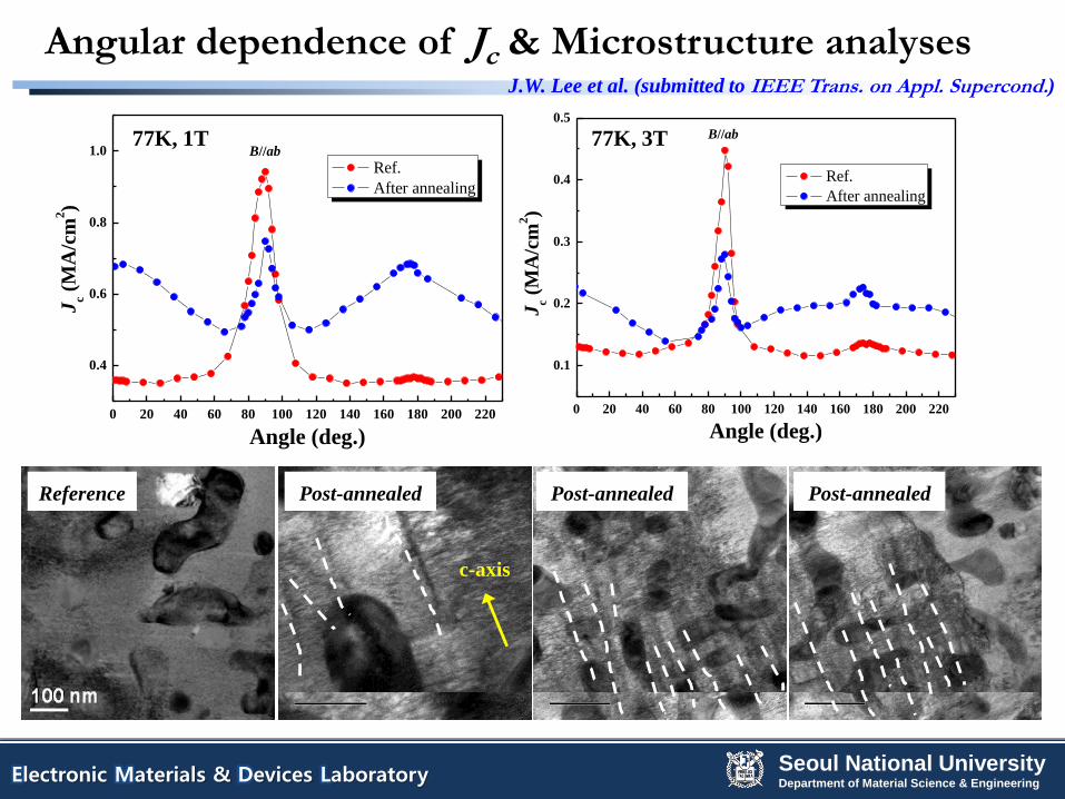
Angular dependence of Jc & Microstructure analyses
0 20 40 60 80 100 120 140 160 180 200 220
0.4
0.6
0.8
1.0 B//ab
Jc (
MA
/cm
2)
Angle (deg.)
Ref.
After annealing
0 20 40 60 80 100 120 140 160 180 200 220
0.1
0.2
0.3
0.4
0.5
Ref.
After annealing
B//ab
Jc (
MA
/cm
2)
Angle (deg.)
77K, 1T 77K, 3T
2 0 0 n m2 0 0 n m
Reference Post-annealed
2 0 0 n m2 0 0 n m
Post-annealed
1 0 0 n m1 0 0 n m
Post-annealed
c-axis
J.W. Lee et al. (submitted to IEEE Trans. on Appl. Supercond.)
Seoul National UniversityDepartment of Material Science & EngineeringElectronic Materials & Devices Laboratory
Optimization of conversion processing from an amorphous
precursor to REBCO film on the basis of phase stability
diagrams in low PO2
Pinning improvement in GdBCO CCs by the RCE-DR process
Defect generation by the post-annealing process
Defect generation by employing the dopants
II. Recent Advances in REBCO CC via RCE-DR

BaSnO3 addition
0 20 40 60 80 1000
100
200
300
400
500
600
700@ 77 K, self-field
10 wt% Sn doped GdBCO
I C
(A
/12m
m)
Length (m)
(From SuNAM)

BaSnO3 addition
In-field performance
0 30 60 900
100
200
300
400
B//cB//ab
10 wt% Sn doped GdBCO (IC,S.F.
=547 A/12mm)
20 wt% Sn doped GdBCO (IC,S.F.
=275 A/12mm)
Undoped GdBCO (IC,S.F.
=720 A/12mm)
I C
(A
/12m
m)
Angle (degree)
@ 77 K, 6300 G
(From SuNAM)

Seoul National UniversityDepartment of Material Science & EngineeringElectronic Materials & Devices Laboratory
41
41
IV. Summary
• The flux pinning properties of GdBCO CCs could be improved by
controlling the conversion temperature of the amorphous precursor film
from Gd2O3 + liquid to the GdBCO phase due to the refinement of Gd2O3
particles trapped in the GdBCO matrix.
• Both Jc-B curves and the angular dependence of Jc of GdBCO CCs reveal
that the flux pinning can be improved by the post-annealing process and
also by the dopant like Sn.
• Further R&D is under progress to develop higher performance REBCO CCs
exceeding GdBCO, which include Y or other RE elements and their binary
or ternary mixture, in addition to a strong effort to improve the pinning
properties of GdBCO CC.
• Our group started R&D on a multicore REBCO tape similar to the BiSCCO
tape (Industry Fund from POSCO).

Seoul National UniversityDepartment of Material Science & EngineeringElectronic Materials & Devices Laboratory
Thank you very much for your kind attention