recent progress in the patterned media
TRANSCRIPT
1 Workshop at U. AL Toshiba Kikitsu1
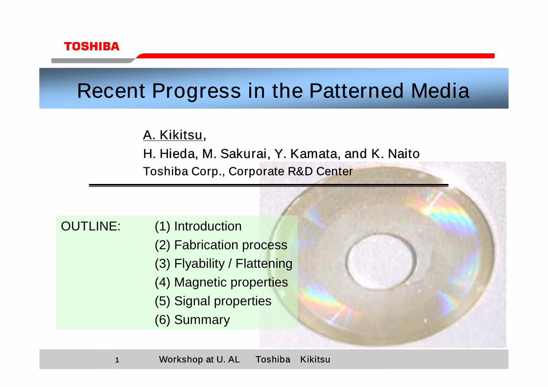
Recent Progress in the Patterned Media
A. Kikitsu,H. Hieda, M. Sakurai, Y. Kamata, and K. NaitoToshiba Corp., Corporate R&D Center
OUTLINE: (1) Introduction(2) Fabrication process(3) Flyability / Flattening(4) Magnetic properties(5) Signal properties(6) Summary

2 Workshop at U. AL Toshiba Kikitsu2
Introduction: concept of the patterned media
20 x 100 nm
patterned media:no thermal fluctuation
current medium:thermal fluctuation ofsmall magnetic grains
recording head
track
NS
NS
NS
NS
SN
SN
SN
NS
NS
NS
NS
SN
SN
SN
NS
NS
NS
NS
SN
SN
SN
NS
NS
NS
NS
SN
SN
SN
NS
NS
NS
NS
SN
SN
SN
NS
NS
NS
NS
SN
SN
SN
data track
recording head
recording medium
magnetic dot;one-bit / dot
<8nm
3 Workshop at U. AL Toshiba Kikitsu3
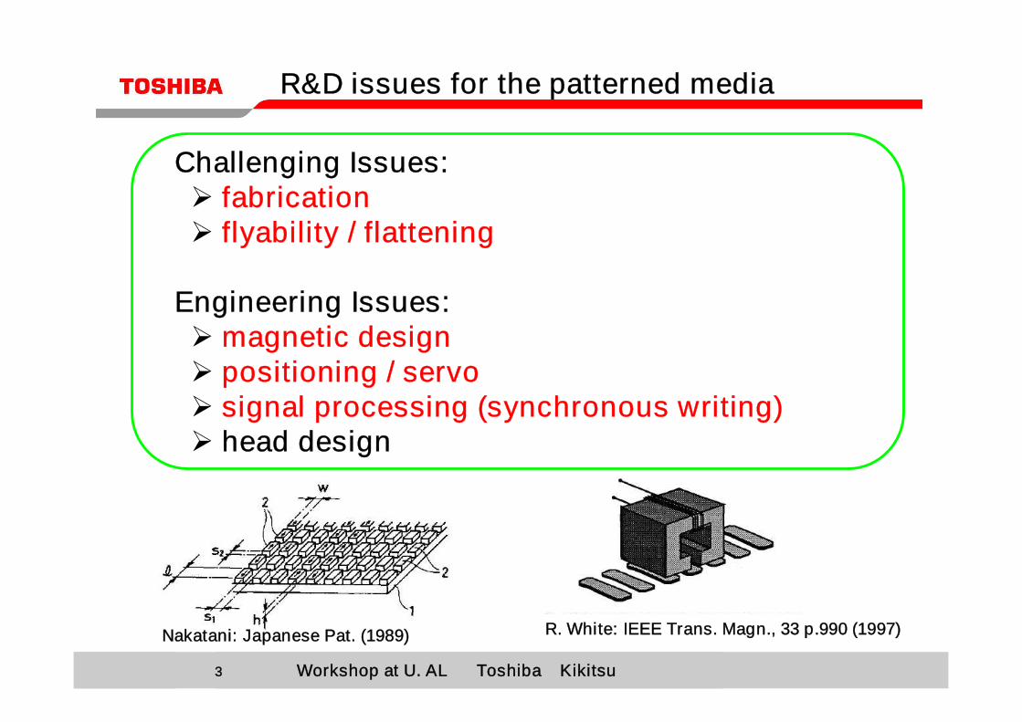
Challenging Issues:fabricationflyability / flattening
Engineering Issues:magnetic designpositioning / servosignal processing (synchronous writing)head design
R&D issues for the patterned media
R. White: IEEE Trans. Magn., 33 p.990 (1997)Nakatani: Japanese Pat. (1989)
4 Workshop at U. AL Toshiba Kikitsu4
(1)fabrication process
highest barrier for the patterned mediadifficulties compare to the semiconductor process
- size ~ cutting edge technology- throughput ~ orders of faster
highest barrier for the patterned mediadifficulties compare to the semiconductor process
- size ~ cutting edge technology- throughput ~ orders of faster
5 Workshop at U. AL Toshiba Kikitsu5
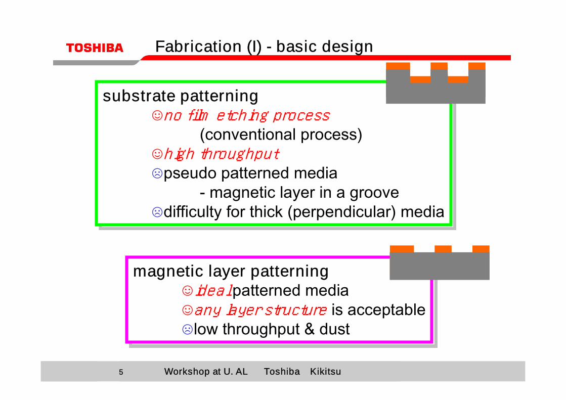
Fabrication (I) - basic design
substrate patterning☺no film etching process
(conventional process)☺high throughput☹pseudo patterned media
- magnetic layer in a groove☹difficulty for thick (perpendicular) media
substrate patterning☺no film etching process
(conventional process)☺high throughput☹pseudo patterned media
- magnetic layer in a groove☹difficulty for thick (perpendicular) media
magnetic layer patterning☺ideal patterned media☺any layer structure is acceptable☹low throughput & dust
magnetic layer patterning☺ideal patterned media☺any layer structure is acceptable☹low throughput & dust
6 Workshop at U. AL Toshiba Kikitsu6
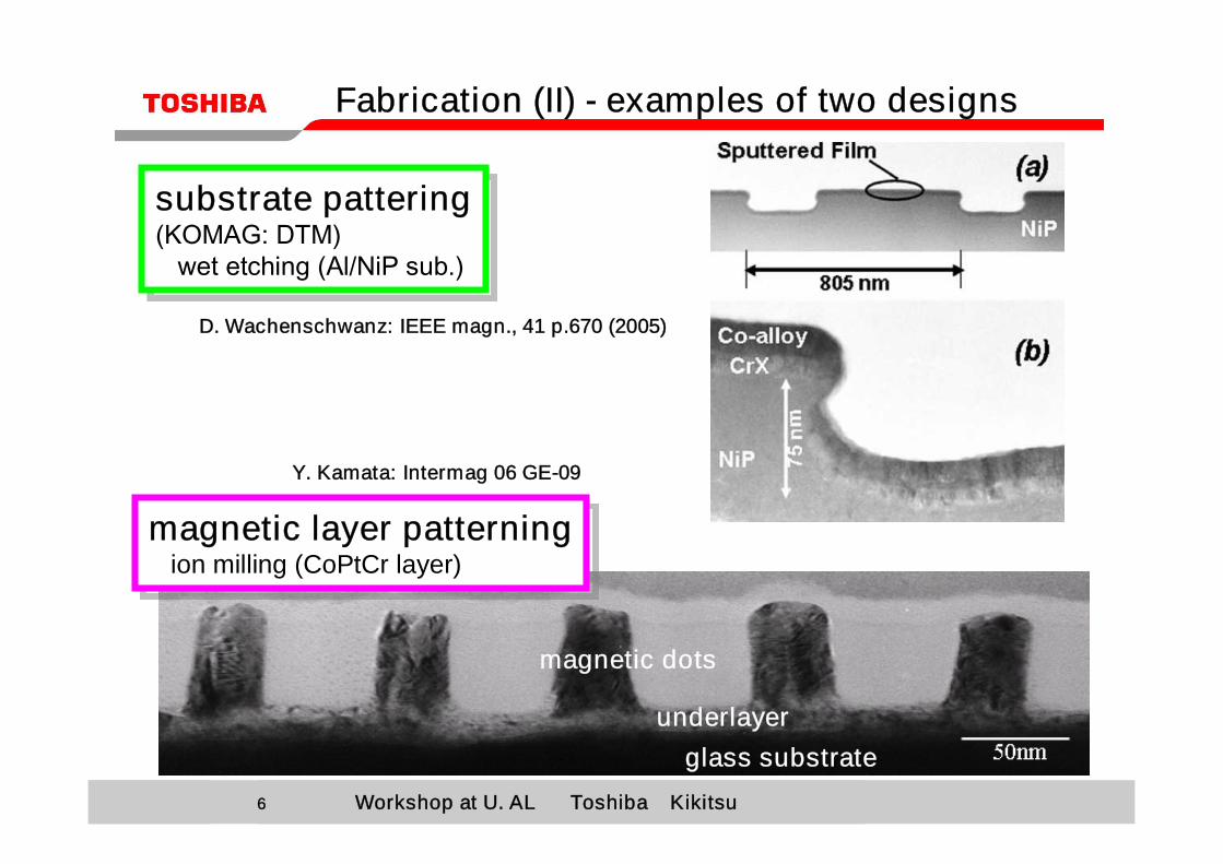
Fabrication (II) - examples of two designs
substrate pattering(KOMAG: DTM)
wet etching (Al/NiP sub.)
substrate pattering(KOMAG: DTM)
wet etching (Al/NiP sub.)
glass substrateunderlayer
magnetic dots
magnetic layer patterningion milling (CoPtCr layer)
magnetic layer patterningion milling (CoPtCr layer)
D. Wachenschwanz: IEEE magn., 41 p.670 (2005)
Y. Kamata: Intermag 06 GE-09
7 Workshop at U. AL Toshiba Kikitsu7
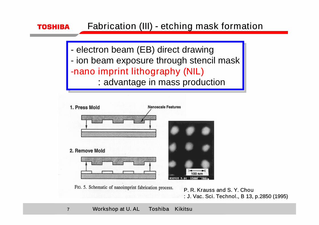
Fabrication (III) - etching mask formation
- electron beam (EB) direct drawing- ion beam exposure through stencil mask-nano imprint lithography (NIL)
: advantage in mass production
- electron beam (EB) direct drawing- ion beam exposure through stencil mask-nano imprint lithography (NIL)
: advantage in mass production
P. R. Krauss and S. Y. Chou : J. Vac. Sci. Technol., B 13, p.2850 (1995)
8 Workshop at U. AL Toshiba Kikitsu8
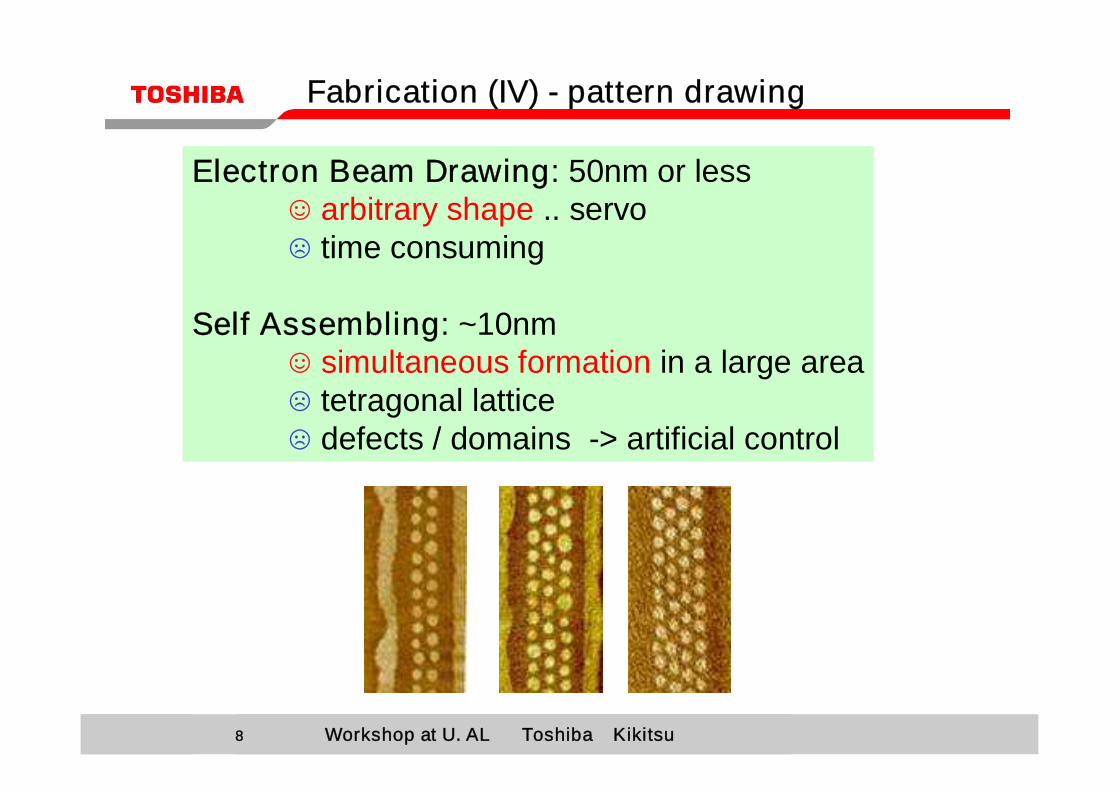
Fabrication (IV) - pattern drawing
Electron Beam Drawing: 50nm or less☺ arbitrary shape .. servo☹ time consuming
Self Assembling: ~10nm☺ simultaneous formation in a large area☹ tetragonal lattice☹ defects / domains -> artificial control
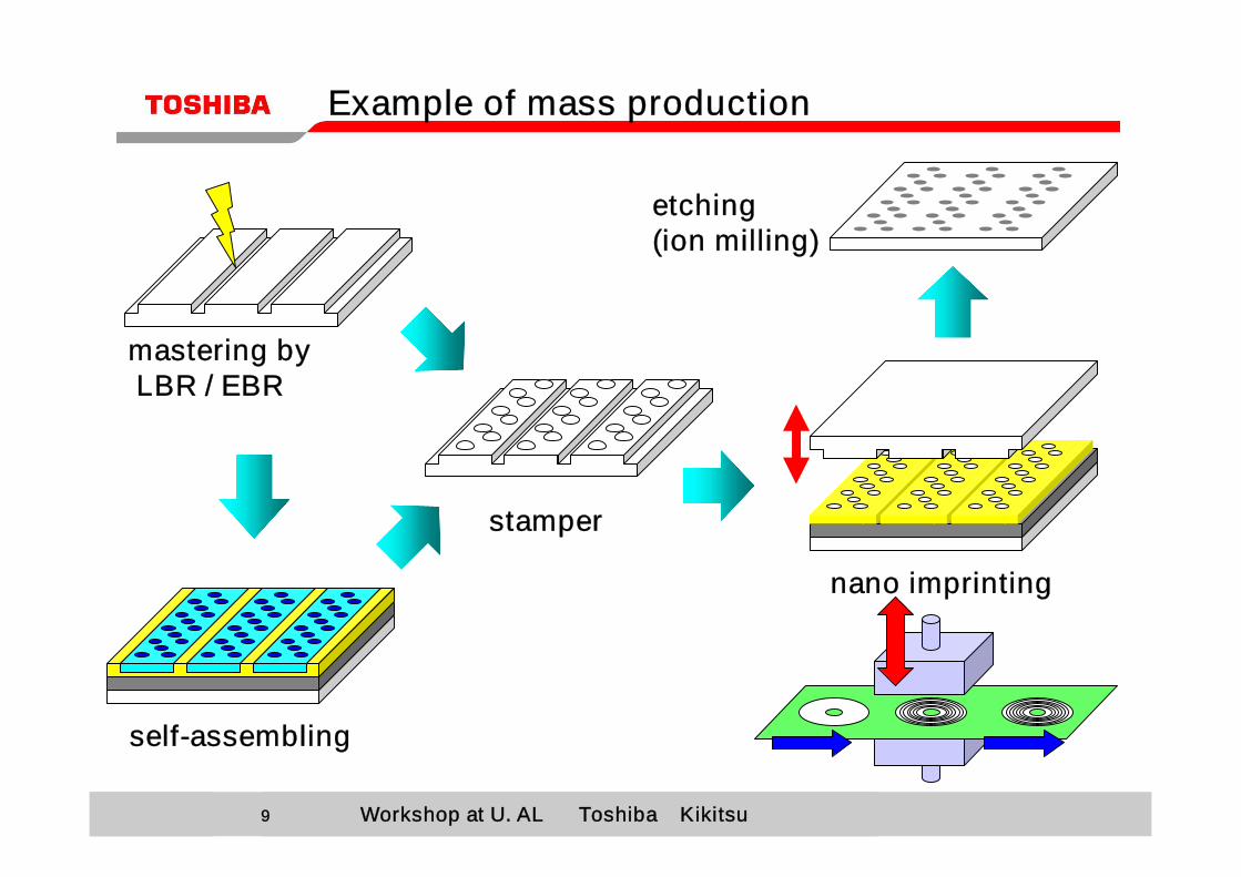
9 Workshop at U. AL Toshiba Kikitsu9
nano imprinting
self-assembling
mastering byLBR / EBR
Example of mass production
stamper
etching(ion milling)
10 Workshop at U. AL Toshiba Kikitsu10
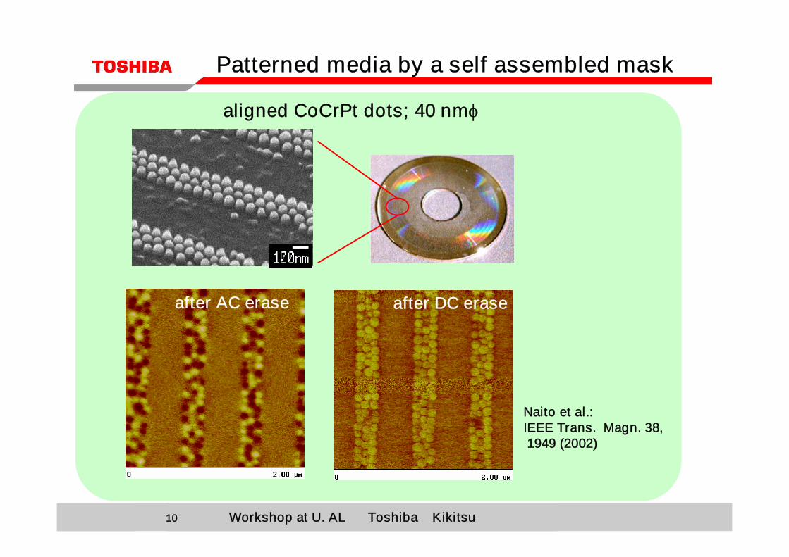
Patterned media by a self assembled mask
after AC erase after DC erase
Naito et al.: IEEE Trans. Magn. 38,1949 (2002)
aligned CoCrPt dots; 40 nm
11 Workshop at U. AL Toshiba Kikitsu11
(2)flyablity / flattening
key issue for high-density HDDflying height < 10nm;
no dust, no debris, no protrusionadditional process -> throughput issue
key issue for high-density HDDflying height < 10nm;
no dust, no debris, no protrusionadditional process -> throughput issue
12 Workshop at U. AL Toshiba Kikitsu12
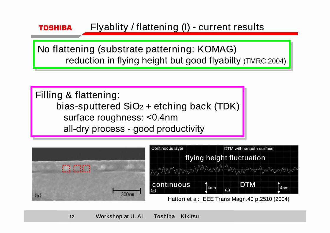
Flyablity / flattening (I) - current results
No flattening (substrate patterning: KOMAG)reduction in flying height but good flyabilty (TMRC 2004)
No flattening (substrate patterning: KOMAG)reduction in flying height but good flyabilty (TMRC 2004)
Filling & flattening:bias-sputtered SiO2 + etching back (TDK)
surface roughness: <0.4nmall-dry process - good productivity
Filling & flattening:bias-sputtered SiO2 + etching back (TDK)
surface roughness: <0.4nmall-dry process - good productivity
Hattori et al: IEEE Trans Magn.40 p.2510 (2004)
flying height fluctuation
continuous DTM
13 Workshop at U. AL Toshiba Kikitsu13
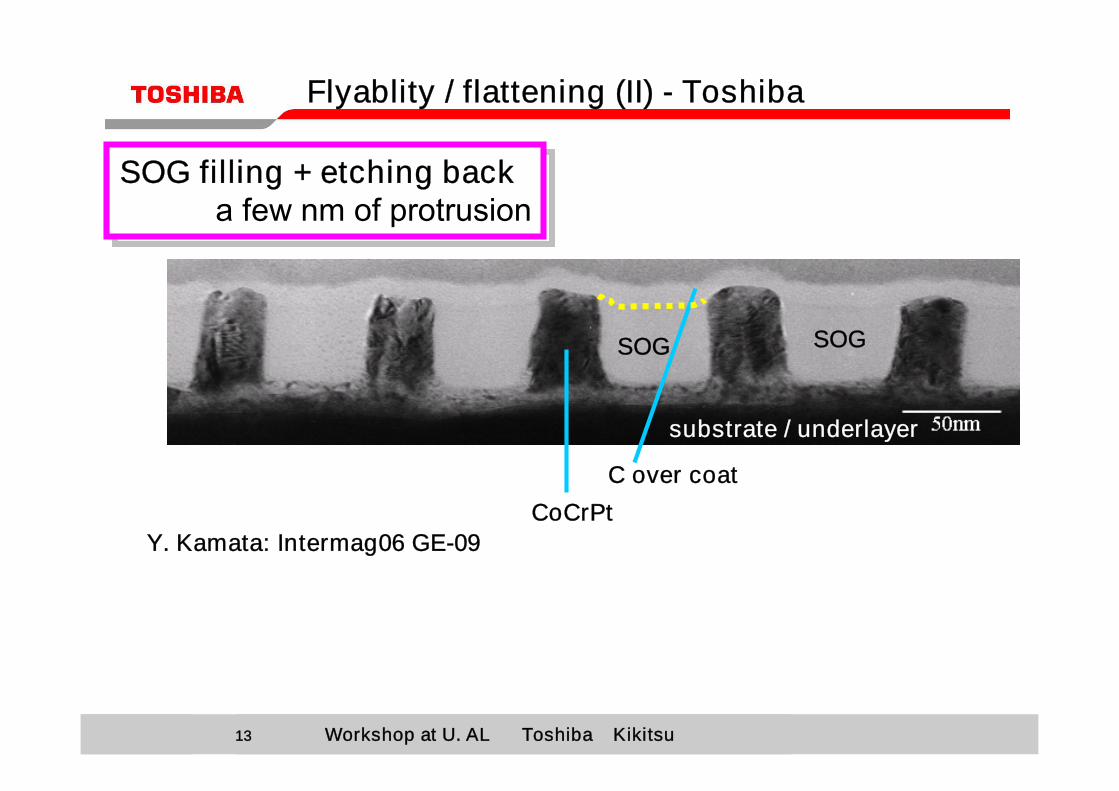
Flyablity / flattening (II) - Toshiba
substrate / underlayer
SOG
CoCrPtC over coat
Y. Kamata: Intermag06 GE-09
SOG filling + etching backa few nm of protrusion
SOG filling + etching backa few nm of protrusion
SOG
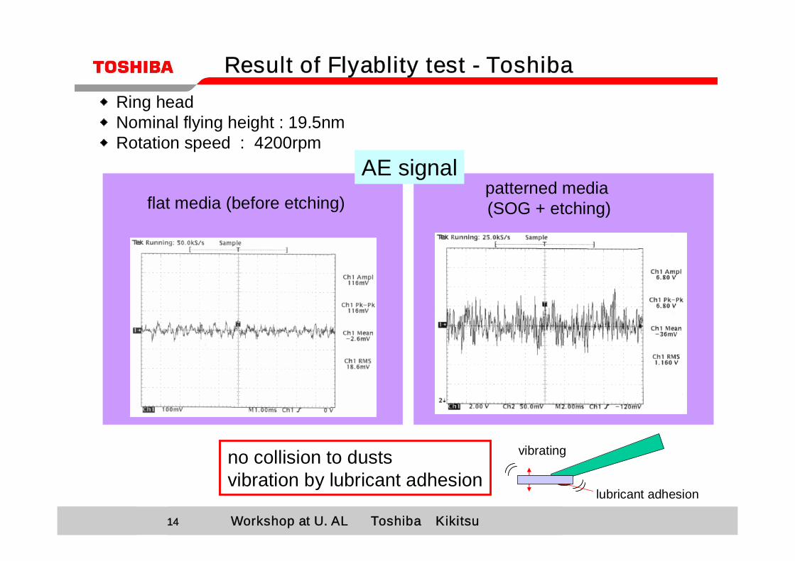
14 Workshop at U. AL Toshiba Kikitsu14
vibrating
lubricant adhesion
flat media (before etching)patterned media (SOG + etching)
Result of Flyablity test - Toshiba◆Ring head◆Nominal flying height : 19.5nm◆Rotation speed : 4200rpm
AE signal
no collision to dustsvibration by lubricant adhesion
15 Workshop at U. AL Toshiba Kikitsu15
(3)magnetic properties
granular -> isolated uniform dotsstrong de-mag fieldmagnetization rotation
granular -> isolated uniform dotsstrong de-mag fieldmagnetization rotation
16 Workshop at U. AL Toshiba Kikitsu16
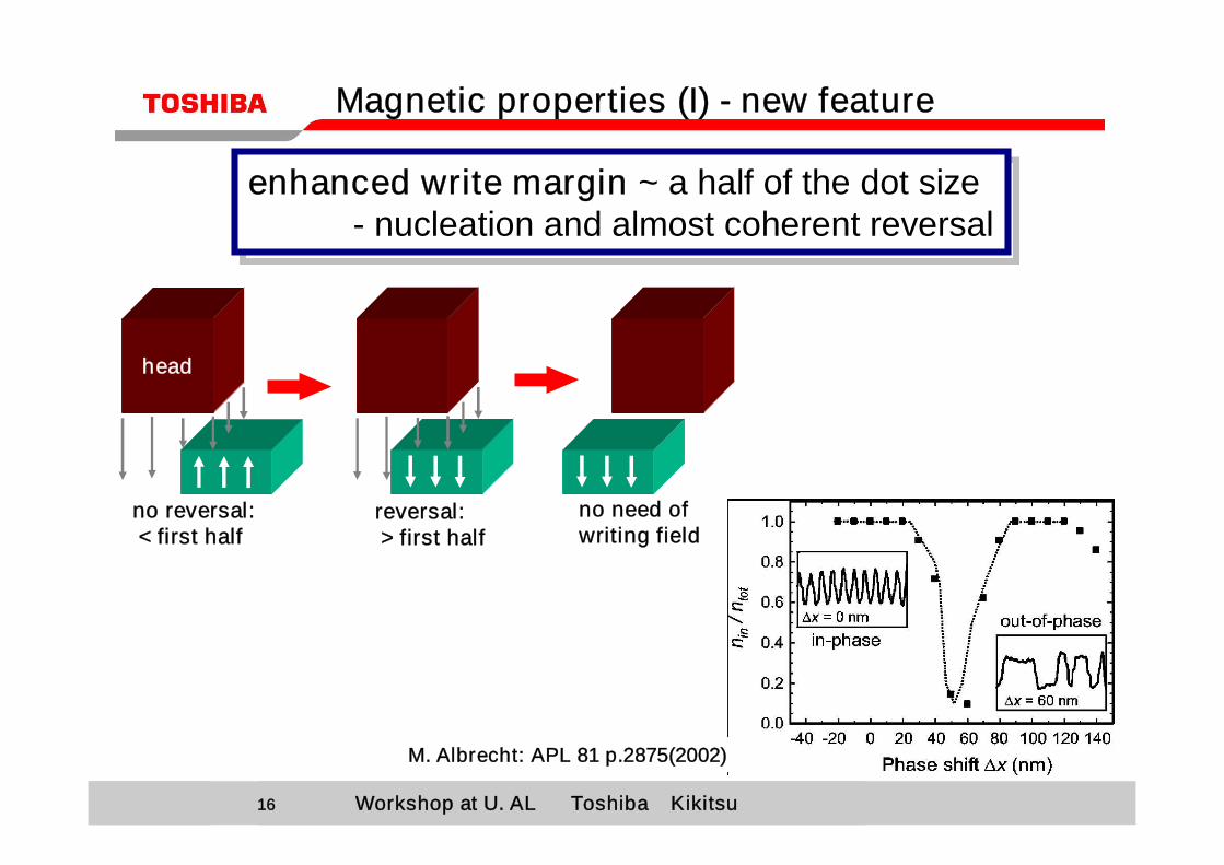
Magnetic properties (I) - new feature
enhanced write margin ~ a half of the dot size- nucleation and almost coherent reversal
enhanced write margin ~ a half of the dot size- nucleation and almost coherent reversal
M. Albrecht: APL 81 p.2875(2002)
head
no reversal:< first half
reversal: > first half
no need ofwriting field
17 Workshop at U. AL Toshiba Kikitsu17
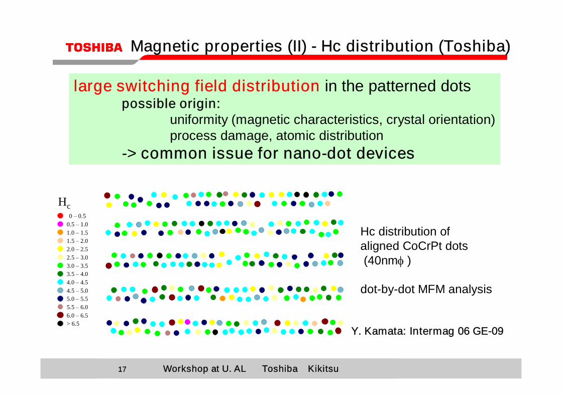
Magnetic properties (II) - Hc distribution (Toshiba)
large switching field distribution in the patterned dotspossible origin:
uniformity (magnetic characteristics, crystal orientation)process damage, atomic distribution
-> common issue for nano-dot devices
Hc distribution of aligned CoCrPt dots(40nm )
dot-by-dot MFM analysis
0 – 0.50.5 – 1.01.0 – 1.51.5 – 2.02.0 – 2.52.5 – 3.03.0 – 3.53.5 – 4.04.0 – 4.54.5 – 5.05.0 – 5.55.5 – 6.06.0 – 6.5> 6.5
Hc0 – 0.5
0.5 – 1.01.0 – 1.51.5 – 2.02.0 – 2.52.5 – 3.03.0 – 3.53.5 – 4.04.0 – 4.54.5 – 5.05.0 – 5.55.5 – 6.06.0 – 6.5> 6.5
Hc
Y. Kamata: Intermag 06 GE-09
18 Workshop at U. AL Toshiba Kikitsu18
(4)signal properties
19 Workshop at U. AL Toshiba Kikitsu19
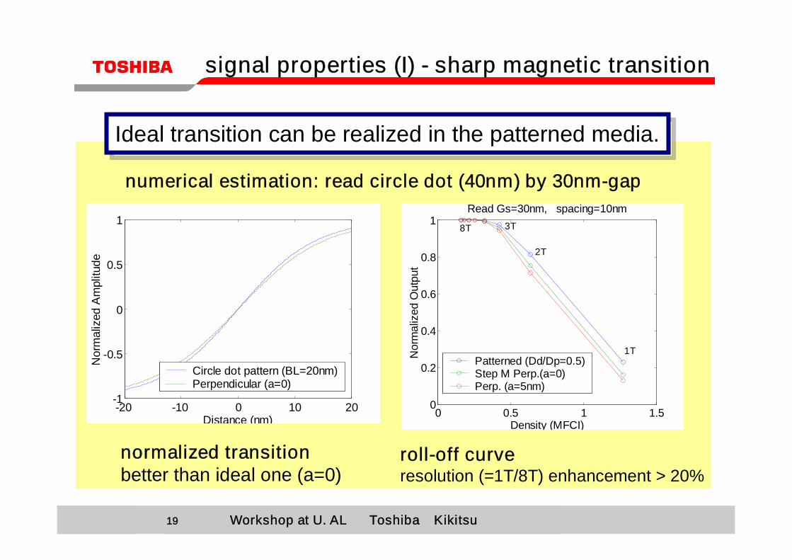
signal properties (I) - sharp magnetic transition
Ideal transition can be realized in the patterned media.Ideal transition can be realized in the patterned media.
-20 -10 0 10 20-1
-0.5
0
0.5
1
Distance (nm)
Nor
mal
ized
Am
plitu
de
Circle dot pattern (BL=20nm)Perpendicular (a=0)
0 0.5 1 1.50
0.2
0.4
0.6
0.8
1
Density (MFCI)N
orm
aliz
ed O
utpu
t
Read Gs=30nm, spacing=10nm
Patterned (Dd/Dp=0.5)Step M Perp.(a=0) Perp. (a=5nm)
1T
2T
3T8T
normalized transitionbetter than ideal one (a=0)
roll-off curveresolution (=1T/8T) enhancement > 20%
numerical estimation: read circle dot (40nm) by 30nm-gap

20 Workshop at U. AL Toshiba Kikitsu20
result of RW test (Toshiba)
MWW:850 nmMRW:600 nm
Trajectory of ring head
on-track off-track
0.5MHz (2kfci)

21 Workshop at U. AL Toshiba Kikitsu21
progress of the patterned media- ☺fabrication
- substrate / mag. etching- nano-imprinting lithography- EB drawing / self assembling .. ~10nm
- ☺ flyablity / flattening .. proven by experiments- no flattening- bias sputtered SiO2 / SOG filling
- ☺ magnetic properties- benefit: wide write margin- distribution in the magnetic properties
- ☺ signal properties- ideal transition is expected
Summary and Conclusion (I)
22 Workshop at U. AL Toshiba Kikitsu22
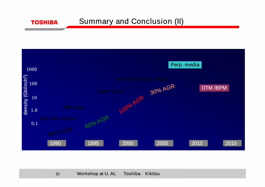
1990 1995 2000 2005 2010 2015
dens
ity (G
b/in
ch2 )
0.1
1.0
10
100
1000
60% AGR
30% AGR
thin film media 100% AGR
30% AGR
MR head
GMR head
Advanced long. media
Perp. media
DTM /BPM
Summary and Conclusion (II)