records of re - beyondinfinite.com · records of revision ... high time tch 10 ... t【nernvi e2】...
TRANSCRIPT


RECORDS OF REVISION MODEL No : LQ197V3DZ82
SPEC No : LD-17825
DATE Rev No. PAGE SUMMARY NOTE
2005.09.06 - - 1st Issue

LD-17825-1
1. Application This specification sheets applies to the color 19.7” VGA TFT- LCD module LQ197V3DZ82. * These specification sheets are proprietary products of SHARP CORPORATION (“SHARP”) and includes materials protected under copyright of SHARP. Do not reproduce or cause any third party to reproduce them in any form or by any means, electronic or mechanical, for any purpose, in whole or in part, without the express written permission of SHARP. * The device listed in these specification sheets was designed and manufactured for use in AV equipment. * In case of using the device for applications such as control and safety equipment for transportation (aircraft, trains, automobiles, and etc), rescue and security equipment and various safety related equipment which require higher reliability and safety, take into consideration that appropriate measures such as fail- safe functions and redundant system design should be taken.
* Do not use the device for equipment that requires an extreme level of reliability, such as aerospace applications, telecommunication equipment (trunk lines), nuclear power control equipment and medical or other equipment for life support.
* SHARP assumes no responsibility for any damage resulting from the use of the device which does not comply with the instructions and the precautions specified in these specification sheets.
* Contact and consult with a SHARP sales representative for any questions about this device. 2. Overview This module is a color active matrix LCD module incorporating amorphous silicon TFT (Thin Film Transistor). It is composed of a color TFT-LCD panel, driver ICs, control circuit, power supply circuit, back light system and etc. Graphics and texts can be displayed on a 640×RGB×480 dots panel with about 16 million colors by supplying date signal of 24 bit(8 bit x RGB), 2 kind of timing signal, +5V of DC supply voltages and supply voltage for back light. 3. Mechanical Specifications
Parameter Specifications Unit 50 (Diagonal) cm Display size 19.7 (Diagonal) inch
Active area 401.28 (H) x 298.8 (V) mm Pixel Format 640 (H) × 480 (V) (1pixel = R + G + B dot)
pixel
Pixel pitch 0.627 (H) × 0.6225 (V) mm Pixel configuration B, G, R vertical stripe Display mode Normally black Unit Outline Dimensions *1 462.6(W) ×338.5(H) × 36.5(D) mm Mass 1960±150 g Surface treatment Anti Glare, low reflection coating
Hard Coating:2H Haze:23 +/- 5 %
(* 1)Outline dimensions are shown in Fig.1

LD-17825-2
4. Input Terminals 4-1. Control circuit driving
CN1 Using connector : 50FLZX-RSM1-A-GB-TB(JST) Pin No. Symbol Function Remarks 1 GND 2 CK Clock signal(sampling each data) 3 GND 4 GND 5 GND 6 DE Data enable signal (Signal to settle the display position) 7 GND 8 R0 Red data signal (LSB) 9 R1 Red data signal 10 R2 Red data signal 11 R3 Red data signal 12 GND 13 R4 Red data signal 14 R5 Red data signal 15 R6 Red data signal 16 R7 Red data signal (MSB) 17 GND 18 G0 Green data signal (LSB) 19 G1 Green data signal 20 G2 Green data signal 21 G3 Green data signal 22 GND 23 G4 Green data signal 24 G5 Green data signal 25 G6 Green data signal 26 G7 Green data signal (MSB) 27 GND 28 B0 Blue data signal (LSB) 29 B1 Blue data signal 30 B2 Blue data signal 31 B3 Blue data signal 32 GND 33 B4 Blue data signal 34 B5 Blue data signal 35 B6 Blue data signal 36 B7 Blue data signal (MSB) 37 GND 38 GND 39 GND 40 GND 41 GND 42 GND 43 GND 44 VDD +5V Power Supply 45 VDD +5V Power Supply 46 VDD +5V Power Supply 47 VDD +5V Power Supply 48 L/R Reverse terminal of Right and Left 【Note 1】 49 U/D Reverse terminal of Up and Down 【Note 1】 50 GND

LD-17825-3
Shield case contacts GND(Ground) of LCD module. Recommended dimensions of FPC/FFC are shown in Fig.2. 4-2. FPC/FFC
Fig.2 Recommended FPC/FFC dimensional diagram
【Note】 Use FFC/FPC which contact point is gold-plated. Contact resistance may increase due to bimetallic corrosion if contact point of FFC/FPC is not gold-plated. 【Note 1】
R/L : L R/L : H U/D : L U/D : L
R/L : L R/L : H U/D : H U/D : H

LD-17825-4
4-3. Back light driving CN 2,3,4,5,6 The module-side connector :BHCR-02VS-5 (JST) The user- side connector : SM02B-BHCS-1, SM02B-BHCS-2 , SM02B-BHCW-1 , SM02B-BHCW-2 (JST) Pin no. symbol Function Cable color 1 V1 Power supply for lamp1 White 【Note1】 2 V2 Power supply for lamp2 Pink 【Note1】
【Note1】Please input the voltage of the opposite phase to V1 and V2.
5. Pixel arrangement and viewing angle Pixel arrangement and viewing angle are as follows.
6. Absolute Maximum Ratings
Parameter Symbol Condition Ratings Unit Remark Input voltage
(for Control PWB) VIC
Ta=25 ℃ -0.3~+3.6 V 【Note 1】
5V supply voltage (for Control PWB)
Vcc Ta=25 ℃ 0~+ 6 V
V1 - 0~3000 Vrms V2 - 0~3000 Vrms
Lamp Incoming voltage
⊿¦V1-V2¦ - 0~3000 Vrms Operation temperature (panel temperature)
Top - 0~+50 ℃ 【Note 2,3】
Storage temperature Tstg - -25~+60 ℃ 【Note 2】 【Note 1】 CK, R0~R7, G0~G7, B0~B7, DE, R/L, U/D
【Note 2】Humidity 95%RH Max.(Ta≦40 ℃) Maximum wet-bulb temperature at 39 ℃ or less.(Ta>40 ℃) No condensation.
【Note 3】Since it becomes as a cause of phenomena, such as contrast unevenness, please make the temperature distribution within a field of a panel uniform.
TFT ‐ LCD (Front side)
②①
CN3
CN2
CN5
CN6
CN4
②①②①②①
①
②
Gate driver
(1,480) (640,480)
12:00
9:00
6:00
3:00
SDR1~SDR5
GDR1
〜GDR2
(1,1) B GR
Source driver (640,1)
Source driver side

LD-17825-5
7. Electrical Characteristics 7-1. Control circuit driving Ta=25 degree
Parameter Symbol Min. Typ. Max. Uniit Remark Supply voltage Vcc +4.5 +5.0 +5.5 V 【Note 1】 +5V supply
voltage Current dissipation
Icc - 340 500 mA 【Note 2】
Permissive input ripple voltage VRP - - 100 mVP-P Vcc=+5.0V Input Low voltage VIL GND - 0.9 V Input High voltage VIH 3.0 - 3.6 V 【Note 3】
Input leak current (Low) IOL1 - - 1.0 μA VI =0V 【Note 3】
Input leak current (High) IOH1 - - 1.0 μA VI =Vcc 【Note 3】
【Note 1】 1) Input voltage sequences
0 < t1 ≦ 10ms, 0 < t2 ≦ 10ms 0 < t3 ≦ 1s, t4 ≧ 1s 2) Dip conditions for supply voltage a) 2.7V ≦ Vcc < 4.5V td ≦ 10ms
b) Vcc < 2.7V Condition of Dip conditions for supply voltage
is based on input voltage sequence.
【Note 2】Typical current situation : 16 gray-bar pattern(Vcc=+5.0V) The explanation of RGB gray scale see section 8. 【Note 3】CK,R0~R7,G0~G7,B0~B7,DE, L/R, U/D
Vcc
td
4
.5V
2
.7V
t1 t2 t3
0.9Vcc 0.9Vcc Vcc
data
Vcc
data
t4
0.1Vcc
0.1Vcc

LD-17825-6
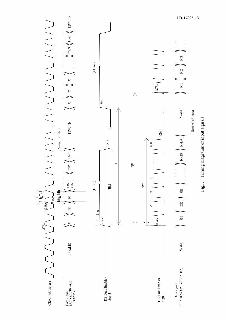
7-2. Timing characteristics of Control circuit input signals Timing diagrams of input signal are shown in Fig.3
Parameter Symbol Min. Typ. Max. Unit Remark Frequency 1/Tc 20.0 25.17 30.0 MHz 【Note 1】High time Tch 10 - - ns CK(Clock) Low time Tc1 10 - - ns Set up time Tds 5 - - ns Data Hold time Tdh 10 - - ns Set up time Tes 7 - Tc-15 ns
Horizontal period TH 790 800 1620 Clock Horizontal period
(High) THd 640 640 640 Clock DE(Data Enable) signal
Vertical period TV 517 525 1000 Line 【Note 2】
Vertical period (High)
TVd 480 480 480 Line
【Note 1】 In case of lower frequency, the deterioration of display quality, flicker, and etc, may occur. 【Note 2】 Be sure to input V0 data during Vertical blanking period. 【Note 3】 It is recommend making sure that length of vertical period is an integral multiple of horizontal length of
period. Otherwise, the screen may not display properly. 7-3.Back Light unit driving The back light unit is an directly under type with five CCFT (Cold Cathode Fluorescent Tube). The characteristics of the lamp are shown in the following table . The value mentioned below is applicable to each individual CCFT .
Parameter Symbol Min. Typ. Max. Unit Remark Lamp current range IL 3.0 6.0 7.0 mArms Lamp voltage VL 1238 1375 1512 Vrms 【Note5】
Ta=25℃,IL=6mA,58kHz Lamp power consumption PL - 8.3 - W 【Note1】
Ta=25℃,IL=6mA, 58kHz Lamp frequency FL 30 58 80 KHz 【Note2】 Kick-off voltage Vs - - 2500 Vrms Ta=0℃ 58kHz
【Note3,5】 Lamp life time LL 50000 - - hour 【Note4】
【Note1】 Referential data per one CCFT by calculation ( IL × VL ) .
The data doesn’t include loss at inverter . 【Note2】 Lamp frequency of inverter may produce interference with horizontal synchronous frequency, and this may
cause horizontal beat on the display. Therefore, adjust lamp frequency, and keep inverter as far as from module or use electronic shielding between inverter and module to avoid interference.
【Note3】The Kick-off voltage may rise up in the user set,please decide the open output voltage by checking not to occur lighting failure under operating state. The voltage above this value should be applied to the lamp for more than 1 second to startup. Otherwise the lamp may not be turned on .
【Note4】Lamp life time is defined as the time when either ① or ② occurs in the continuous operation under the condition of Ta=25℃ and IL=6.0mArms .
① Brightness becomes 50% of the original value under standard condition . ② Kick-off voltage at Ta=0℃ exceeds maximum value, 2160Vrms .
Definition is based upon when the longer edge of the LCD module is placed horizontally (in landscape position)The length of LCD module’s life time may vary if the module is placed vertically (in a portrait position), due to the lopsided mercury in the CCFT lamps.

LD-17825-7
【Note5】In antiphase drive, the voltage of one side would be the half of the value mentioned above table. 《Note》The performance of the back light, for example life time or brightness, is much influenced by the
characteristics of the DC-AC inverter for the lamp .When you design or order the inverter, please make sure that a poor lighting caused by the mismatch of the back light and the inverter (miss- lighting, flicker, etc.) never occurs . When you confirm it, the module should be operated in the same condition as it is installed in your instrument . Use the lamp inverter power source incorporating such safeguard as overvoltage / overcurrent protective circuit or lamp voltage waveform detection circuit, which should have individual control of each lamp. In case one circuit without such individual control is connected to more than two lamps, excessive current may flow into one lamp when the other one is not in operation.
(1line)
(2line)
(R0~
R7,G
0~G
7,B0~
B7)
LD-17825 - 8
DE(
Dat
a En
able
) sig
nal
CK(C
lock
sign
al)
Numberofdata
Dat
a sig
nal
(R0~
R7,G
0~G
7
B0~
B7)
INVALID
INVALID
D639
D640
0.3Vcc
TH
TdsTdh
D1D2
D30.7Vcc
0.3Vcc
0.7Vcc
Tes
THd
Dat
a sig
nal
DH479
DH480
Numberofdata
INVALID
DH1
DH2
DH3
TV
INVALID
0.7Vcc
DH1
DH2
DH3
0.7Vcc
D1D2
D3
0.7Vcc
D639
D640
INVALID
TchTcl
Tc
0.7Vcc
0.7Vcc 0.3Vcc
DE(
Dat
a En
able
) sig
nal
0.3Vcc
TVd
1 2
3 4
480
Fig3
. T
imin
g di
agra
ms o
f inp
ut si
gnal
s

LD-17825-9
8. Input Signal, Basic Display Colors and Gray Scale of Each Color Data signal
Color & Gray scale Gray
Scale R0 R1 R2 R3 R4 R5 R6 R7 G0 G1 G2 G3 G4 G5 G6 G7 B0 B1 B2 B3 B4 B5 B6 B7
Black - 0 0 0 0 0 0 0 0 0 0 0 0 0 0 0 0 0 0 0 0 0 0 0 0Blue - 0 0 0 0 0 0 0 0 0 0 0 0 0 0 0 0 X X 1 1 1 1 1 1Green - 0 0 0 0 0 0 0 0 X X 1 1 1 1 1 1 0 0 0 0 0 0 0 0Cyan - 0 0 0 0 0 0 0 0 X X 1 1 1 1 1 1 X X 1 1 1 1 1 1Red - X X 1 1 1 1 1 1 0 0 0 0 0 0 0 0 0 0 0 0 0 0 0 0Magenta - X X 1 1 1 1 1 1 0 0 0 0 0 0 0 0 X X 1 1 1 1 1 1Yellow - X X 1 1 1 1 1 1 X X 1 1 1 1 1 1 0 0 0 0 0 0 0 0
Basic Color
White - X X 1 1 1 1 1 1 X X 1 1 1 1 1 1 X X 1 1 1 1 1 1Black GS0 0 0 0 0 0 0 0 0 0 0 0 0 0 0 0 0 0 0 0 0 0 0 0 0× GS1 1 0 0 0 0 0 0 0 0 0 0 0 0 0 0 0 0 0 0 0 0 0 0 0Darker GS2 0 1 0 0 0 0 0 0 0 0 0 0 0 0 0 0 0 0 0 0 0 0 0 0× È È È È Ø È È È È
Brighter GS250 0 1 0 1 1 1 1 1 0 0 0 0 0 0 0 0 0 0 0 0 0 0 0 0Ø GS251 1 1 0 1 1 1 1 1 0 0 0 0 0 0 0 0 0 0 0 0 0 0 0 0
Gray Scale of Red
Red GS252 X X 1 1 1 1 1 1 0 0 0 0 0 0 0 0 0 0 0 0 0 0 0 0Black GS0 0 0 0 0 0 0 0 0 0 0 0 0 0 0 0 0 0 0 0 0 0 0 0 0× GS1 0 0 0 0 0 0 0 0 1 0 0 0 0 0 0 0 0 0 0 0 0 0 0 0Darker GS2 0 0 0 0 0 0 0 0 0 1 0 0 0 0 0 0 0 0 0 0 0 0 0 0× È È È È Ø È È È È
Brighter GS250 0 0 0 0 0 0 0 0 0 1 0 1 1 1 1 1 0 0 0 0 0 0 0 0Ø GS251 0 0 0 0 0 0 0 0 1 1 0 1 1 1 1 1 0 0 0 0 0 0 0 0
Gray Scale of Green
Green GS252 0 0 0 0 0 0 0 0 X X 1 1 1 1 1 1 0 0 0 0 0 0 0 0Black GS0 0 0 0 0 0 0 0 0 0 0 0 0 0 0 0 0 0 0 0 0 0 0 0 0× GS1 0 0 0 0 0 0 0 0 0 0 0 0 0 0 0 0 1 0 0 0 0 0 0 0Darker GS2 0 0 0 0 0 0 0 0 0 0 0 0 0 0 0 0 0 1 0 0 0 0 0 0× È È È È Ø È È È È
Brighter GS250 0 0 0 0 0 0 0 0 0 0 0 0 0 0 0 0 0 1 0 1 1 1 1 1Ø GS251 0 0 0 0 0 0 0 0 0 0 0 0 0 0 0 0 1 1 0 1 1 1 1 1
Gray Scale of Blue
Blue GS252 0 0 0 0 0 0 0 0 0 0 0 0 0 0 0 0 X X 1 1 1 1 1 10 :Low level voltage, 1 :High level voltage, Each basic color can be displayed in 253 gray scales with 8 bit data signals. According to the combination of total 18 bit data signals, the 16-million-color display can be achieved on the screen. (X: don’t care)

LD-17825-10
9. Optical characteristics Ta=25[℃], Vcc=+5[V], IL=6.0[mA]
Parameter Symbol Condition Min. Typ. Max. Unit Remark
Horizontal θ21, θ22
80 85 - Deg. Viewing angle range Vertical
θ11 θ12
CR≧10
80 85 - Deg.
【Note1,2】 Fig.10
Contrast ratio CRn Best ViewingAngle
500 600 - 【Note2】 Fig.11
Response time τr+τd - 20 30 ms 【Note3】 Fig.11
Chromaticity of white X 0.242 0.272 0.302 - Y 0.248 0.278 0.308 -
Chromaticity of Red X 0.610 0.640 0.670 - Y 0.307 0.337 0.367 -
Chromaticity of Green X 0.240 0.270 0.300 - Y 0.576 0.606 0.636 -
Chromaticity of Blue X 0.114 0.144 0.174 - Y 0.040 0.070 0.100 -
Luminance of white YL1 360 450 - cd/m2
【Note 4,7】
Luminance uniformity δW
θ=0℃
- - 1.25 - 【Note 6,7】 *The measurement shall be executed 30 minutes after lighting at rating. Optical characteristic measurement is performed in a darkroom or the state equivalent to this using the measuring method of the following figure.
Middle of the screen(θ=0°)
TFT-LCD Module
Middle of the screen(θ=0°)
TFT-LCD Module
400mm
Field=2°
Detector(SR-3/BM-5A) Detector(EZ-CONTRAST)
Measurement of Contrast and viewing angle range Measurement of luminance and chromaticity and Response time (Response time:BM-5A,Other:SR-3)
Fig.4 Optical characteristics measurement method

LD-17825-11
【Note 1】Definitions of viewing angle range : Fig.12
【Note 2】Definition of contrast ratio : The contrast ratio is defined as the following. Contrast Ratio (CR) =
【Note 3】Definition of response time
The response time is defined as the following figure.13 and shall be measured by switching the input signal for “black” and “white”.
【Note 4】This shall be measured at center of the screen. 【Note 5】Temperature of panel surface shall be 40 degree. 【Note 6】Definition of white uniformity ;
White uniformity is defined as the following with five measurements.(A~E) δW=
【Note7】The setting value of a use inverter a)Lamp current: 6mArms b)Frequency: 58kHz
Luminance(brightness) with all pixels white
Luminance(brightness) with all pixels black
maximum Luminance of five points(brightness) minimum Luminace of five points(brightness)
Normal line
θ21θ11
θ12 θ22
6 o’clock direction
Wd Wr
0% 10%
90% 100%
White white black
time
Photodetector
Output
Fig.12

LD-17825-12
10. Display Quantity The display quality of the color TFT-LCD module shall be in compliance with the Incoming Inspection Standard.
11. Handling Precautions of the module
a) Be sure to turn off the power supply when inserting disconnecting the cable. b) This product is using the parts(CCFT etc) which generate the high voltage. Therefore, during operating, please don't touch these parts.
c) Be sure to fix the module in the same plane so that the module can be installed without any extra stress such as warp or twist.
d) Since the front polarizer is easily damaged, pay attention to treat it. e) Since long contact with water may cause discoloration or spots, wipe off water drop immediately. f) When the panel surface is soiled, wipe it with absorbent cotton or other soft cloth. g) Since the panel is made of glass, it may break or crack if dropped or bumped on hard surface. Handle with care.
h) Since CMOS LSI is used in this module, take care of static electricity and consider wearing the earth personnel when handling.
i) Ground attachment to the LCD module should be considered, so that influences from EMI and outer noise is minimized.
j) The module has some printed circuit boards (PCBs) and cable harness on the back side, take care to keep them form any stress or pressure when handling or installing the module; otherwise some of electronic parts on the PCBs and cable harness may be damaged.
k) Observe all other precautionary requirements in handling components. l) When some pressure is added onto the module from rear side constantly, it causes display non-uniformity issue, functional defect, etc.. So, please avoid such design
m) When handling LCD modules and assembling them into cabinets, please be noted that long- term storage in the environment of oxidization or deoxidization gas and the use of such materials as reagent, solvent, adhesive, resin, etc. which generate these gasses, may cause corrosion and discoloration of the LCD modules.
n) Blow off dust with N2 blower for which static electricity preventive measure has been taken. Ionized air gun is recommended.
12. Packing form
a) Piling number of cartons: 3(maximum) b) Packing quantity in one carton : 10 c) Carton size : 706mm(W) × 532mm(D) × 421mm(H) d) Total mass of one carton filled with full modules : 22Kg

LD-17825-13
13. Reliability test items No Test item Conditions 1 High temperature storage test Ta = 60℃ 240h 2 Low temperature storage test Ta = -25℃ 240h 3 High temperature & high humidity operation test
Ta = 40℃ ; 95%RH 240h (No condensation)
4 High temperature operation test Ta = 50℃ 240h (The panel temperature must be less than 60℃)
5 Low temperature operation test Ta = 0℃ 240H 6 Vibration test (non- operating)
Waveform : Sine wave Frequency : 10~57Hz/Vibration width (one side) : 0.075mm : 57~500Hz/Gravity : 9.8m/s2 Sweep time : 11minutes Test period : 3 hours (1 hour for each direction of X,Y,Z)
7 Shock test (non- operating)
Max. gravity : 490m/s2 Pulse width : 11ms, sine wave
Direction : ±X, ±Y, ±Z, once for each direction.
8 Thermal shock test (non- operating )
Ta=-25℃~60℃ ; 5 cycles Test period : 10 hours (1 hour for each temperature)
9 ESD test
Contact discharge method : C=150pF,R=330Ω (non- operating) Pass +/- 15kV (operating) Pass +/- 8kV Air discharge method : C=150pF,R=330Ω (non- operating) Pass +/- 20kV (operating) Pass +/- 10kV
【Result evaluation criteria】 Under the display quality test conditions with normal operation state, these shall be no change which may affect practical display function.
14. Others
1) Lot No. Label
* Lot Number is printed on Barcode. * Label color is white, and Characters are black.
SHARP LQ197V3DZ82 59 00000001
MADE IN JAPAN
Model No.
Lot No
Bar Code
(Lot No.)
How to express Lot No.
A production month (1̃ 9 ,X, Y, Z)
Serial No.
A production year (the last figures of the Christian Era)
Production country indication Japanese products : "MADE IN JAPAN" Chinese products : "MADE IN CHINA" Malaysian products : "MADE IN MALAYSIA"
SHARP management No.

LD-17825-14
2) Packing Label ① Model No. (LQ197V3DZ82)
② Lot No. (Date)
③ Quantity
3) Adjusting volume have been set optimally before shipment, so do not change any adjusted value. If adjusted
value is changed, the specification may not be satisfied. 4) Disassembling the module can cause permanent damage and should be strictly avoided. 5) Please be careful since image retention may occur when a fixed pattern is displayed for a long time. 6) Turn off the inverter circuit for back light before turning off the power source for the controller. 7) Rust is out of considerations. 8) Regulation on usage of destructible chemical substances for the Ozone layer
Regulated substances:CFCS、Quadru Carbon Chloride、1,1,1-Tri chloro-ethylene (MethylChloroform) a) above mentioned substances are not used in the product, and/or assembled unit and parts of this product
b) above mentioned substances are not used in the process of manufacturing the product and/or assembled unit and parts of this product.
9) Marking of using material information It is displaying the material of the optical parts with the label in the module back.
10) Cold cathode fluorescent lamp in LCD panel contains a small amount of mercury, Please follow local ordinances or regulations for It displays it on the back of the module as follows.
11) When any question or issue occurs, it shall be solved by mutual discussion.
社内品番:(4S)LQ197V3DZ82
LotNO. :(1T)2005.※.※※
Quantity:(Q) 10pcs
ユーザ品番 :
Bar code(①)
Bar code(②)
Bar code(③)
シャープ物流用ラベルです。 *****
MATERIALINFORMATION
DIFFUSER SHEET:>PMMA-X,PET< DIFFUSER BOARD:>SMMA,PS<
LENS FILM:>PET,AK-X<

LD-17825-15
15. Storage conditions <Environmental condition range of storage temperature and humidity> Temperature 0 to 40 degrees Celsius Relative humidity 95% and below 【Note】 Please refer below as a mean value of the environmental conditions. Summer time temperature 20 to 35 degrees Celsius humidity 85% and below Winter time temperature 5 to 15 degrees Celsius humidity 85% and below Please maintain within 240 hours of accumulated length of storage time, with conditions of 40 degrees
Celsius and room humidity of 95%. Direct sun light Please keep the product in a dark room or cover the product to protect from direct sun light. Atmospheric condition Please refrain from keeping the product with possible corrosive gas or volatile flux. Prevention of dew * Please store the product carton either on a wooden pallet or a stand / rack to prevent
dew. Do not place directly on the floor. In addition, to obtain moderate ventilation in between the pallet’s top and bottom surfaces, pile the cartons up in a single direction and in order. * Please place the product cartons away from the storage wall. * Please maintain the storage area with an appropriate ventilation. It is recommendable to furnish the storage area with equipments such as ventilation systems.
* Please maintain the ambient temperature within the range of natural environmental fluctuation.
Storage period Within above mentioned conditions, maximum storage period should be one year.

