redacted for privacy - core
TRANSCRIPT

AN ABSTRACT OF THE THESIS OF
Devavrata Godbole for the degree of Master of Science in
Electrical amp Computer Engineering presented on October 3 2000 Title
PHASE NOISE MODELS FOR SINGLE-ENDED RING OSCILLATORS
Abstract approved ___ qt- ___
John T Stonick
The tremendous growth of wireless and mobile communications has resulted in placing
of stringent requirements on the channel spacing and by implication on the phase noise
of oscillators typically mandating the use of passive LC oscillators with high quality
factor (Q) However the trend towards large-scale integration and low cost makes it
desirable to implement ring oscillators monolithically using CMOS but they generally
have inferior phase noise performance compared to LC oscillators Currently there is
no tool available for the designer to analyze the effect of oscillator phase noise on the
performance of the communication system Thus an accurate and efficient system level
model for oscillator phase noise which can be used in simulation is of great importance
In this thesis two system level phase noise models accurate at the circuit level namely
Hajimiri Phase Noise model and Digital FIR Filter model for Phase Noise are discussed
and implemented in MATLABs SIMULINK environment to bridge the gap in tools
available for circuit level design and system level design of communication systems
Redacted for Privacy
copyCopyright by Devavrata Godbole
October 3 2000
All rights reserved
PHASE NOISE MODELS FOR SINGLE-ENDED RING OSCILLATORS
by
Devavrata Godbole
A THESIS
submitted to
Oregon State University
in partial fulfillment of the requirements for the
degree of
Master of Science
Presented October 3 2000 Commencement June 2001
Master of Science thesis of Devavrata Godbole presented on October 3 2000
APPROVED
Major Pr essor representmg Electncal amp Computer Engmeermg
of Electrical amp Computer Engineering
I understand that my thesis will become part of the permanent collection of Oregon State University libraries My signature below authorizes release of my thesis to any reader upon request
Devavrata Godbole Author
Redacted for Privacy
Redacted for Privacy
Redacted for Privacy
Redacted for Privacy
ACKNOWLEDGMENT
I would like to express my deepest appreciation and thanks to my thesis advisor
Prof John T Stonick for his great enthusiasm in research and invaluable guidance during
my research His passion for teaching and learning has always been a great source of
inspiration for me My appreciation also reaches friends and colleagues I have got to
know during these two years This thesis would not have been completed without their
continuous help and moral support Finally and most importantly I want to express
my sincerest gratitude to my dearest parents for always being there for me No amount
of thanks would be too much for their constant love encouragement and support
dedicate this thesis to them
I
TABLE OF CONTENTS
Page
1 INTRODUCTION 1
11 Definition of Phase Noise and Jitter in Oscillators 1
111 What is Phase Noise 1 112 Units of Oscillator Phase Noise 2 113 What is Jitter 3
12 Importance of Phase Noise Specifications for Communication Systems 4
13 Advantages of Ring Oscillators 6
14 Problem Statement 7
2 HAJIMIRI PHASE NOISE MODEL 10
21 Salient Features 10
22 Explanation 10
23 Conversion of Device Noise to Phase Fluctuations 13
24 Phase-to-Voltage Transformation 16
25 Conversion of Ring Oscillator Device Noise to Phase Noise 16
26 Reducing the Effect of Flicker Noise on Oscillator Phase Noise 19
27 Calculation of Phase Noise Spectrum for Ring Oscillators 23
28 Comparison of Hajimiri Phase Noise Model with SpectreRF PSS Phase Noise Analysis 24
281 Simulation Results for 3-Stage Single-Ended Ring Oscillator Implemented using HP 08J-lm Process having Oscillation Freshyquency 315 MHz 25
282 Simulation Results for 3-Stage Ring Oscillator using HP 08J-lm Process having Oscillation Frequency 500 MHz 29
283 Simulation Results for 3-stage Ring Oscillator using HP 12J-lm Process having Oscillation Frequency 154 MHz 29
29 MATLAB Graphic User Interface (GUI) for Hajimiri Phase Noise Model 31
TABLE OF CONTENTS (Continued)
Page
210 Generation of ISF for the User-Specified Ring Oscillator 33
211 Implementation of Hajimiri Phase Noise Model for Single-Ended Ring Oscillators in SIMULINK 36
2111The SIMULINK Environment 36 2112Hajimiri Phase Noise Model Implementation in SIMULINK 38 2113Improving the Efficiency of Hajimiri Phase Noise Model Impleshy
mented in SIMULINK 39
212 Verification of Fast SIMULINK Method for Hajimiri Phase Noise Model Implementation 40
2121MATLAB Test Simulations 41 2122Simulation for Symmetrical ISF 41 2123Simulation for Non-Symmetrical ISF 42
213 SIMULINK s-Function Implementation of Fast Hajimiri Phase Noise Model 46
3 IMPLEMENTATION OF PHASE NOISE MODEL USING DIGITAL FILshyTER 48
31 Calculating the Phase Disturbance Response from the Oscillators PSD 48
32 MATLAB GUI Designed for the Design of FIR Filter 52
4 LOCAL OSCILLATOR MODEL IMPLEMENTED IN COMMIC 54
5 CONCLUSIONS 60
BIBLIOGRAPHy 61
LIST OF FIGURES
Figure Page
11 Frequency spectrum of an ideal sinusoidal oscillator 1
12 Frequency spectrum of a sinusoidal oscillator having phase noise 2
13 Phase noise measurement 3
14 Jitter 3
15 PLL system 4
16 Generic transreceiver 5
17 Ideal case 6
18 Effect of phase noise on the receive path 8
19 Effect of phase noise on the transmit path 9
110 LC oscillator 9
21 Phase and amplitude response model 11
22 (a) Ideal LC oscillator (b) Impulse injected at the peak (c) Impulse at zero crossing 12
23 Conversion of input noise to output phase noise 13
24 ISF decomposition 14
25 Current noise conversion to excess phase 15
26 Noise in MOSFET 16
27 Conversion of MOSFET device noise to phase disturbance and then to phase noise sidebands 18
28 Non-symmetrical ISF waveform for the oscillator having non-symmetrical rise and fall times 20
29 Symmetrical ISF waveform for the oscillator with scaled PMOS device 21
210 (a) Input Waveform (b) Single-stage circuit (c) Trajectory of the outshyput as the input goes high and C discharges through QN 22
211 Cadence schematic of 3-stage ring oscillator 24
LIST OF FIGURES (Continued)
Figure
212 ISF for 3-Stage ring oscillator obtained using SpectreS and HSPICE simulations 26
213 Phase noise spectrum plot from Hajimiri phase noise model calculated using ISF obtained from SpectreS and HSPICE simulations 27
214 Phase noise spectrum using SpectreRF PSS analysis and Hajimiri phase noise model 28
215 Thermal noise analysis circuit for HP 08J-lm NMOS process 29
216 Phase noise spectrum using SpectreRF PSS analysis and Hajimiri phase noise model for 500 MHz oscillation 30
217 Phase noise spectrum using SpectreRF PSS analysis and Hajimiri phase noise model for 151 MHz oscillation using HP 12J-lm process 31
218 MATLAB Graphic User Interface flow diagram 33
219 3-Stage single-ended ring oscillator with current impulse 35
220 Current Impulse applied at node 1 of ring oscillator 36
221 GUI figure for Hajimiri phase noise model 37
222 Symmetrical ISF plot 43
223 Plot of disturbance in oscillator phase for symmetrical ISF case 43
224 Comparison plot of frequency spectrums of phase disturbance genershyated using the two methods in dBc for symmetrical ISF case 44
225 Non-symmetrical ISF plot 44
226 Plot of disturbance in oscillator phase for non-symmetrical ISF case 45
227 Comparison plot of frequency spectrums of phase disturbance genershyated using the two methods in dBc for non-symmetrical ISF case 45
228 Flow diagram of SIMULINK based fast Hajimiri phase noise model 47
31 Oscillators frequency response 49
32 Generation of oscillators phase disturbance using digital FIR filter 51
33 MATLAB GUI for digital FIR filter design 53
LIST OF FIGURES (Continued)
Figure Page
41 Communication IC toolbox 54
42 LO block in simulink 55
43 Selection of Hajimiri phase noise model for LO block 56
44 Selection of digital filter model for LO block 57
45 Mask of LO model 58
46 Hajimiri phase noise model mask 58
47 Digital FIR filter mask 59
PHASE NOISE MODELS FOR SINGLE-ENDED RING OSCILLATORS
1 INTRODUCTION
11 Definition of Phase Noise and Jitter in Oscillators
111 What is Phase Noise
The output of an ideal oscillator with no noise can be expressed as
VLOoutput = Af[wet + cent]
where A is the peak amplitude of the oscillator We is the oscillator frequency and f the
oscillator phase Note that in the case of an ideal oscillator A We and f are all constants
The one-sided frequency of such an ideal oscillator looks as in Fig 11
However in a practical oscillator due to the presence of noise the output is given
by
VLOoutput = A(t)J[wet + cent(t)]
where A(t) and cent(t) represent the fluctuations in peak amplitude and phase of the
oscillator output and are no longer constants As a consequence of the fluctuations in
oscillators phase and amplitude the spectrum of a practical oscillator has skirts close
Frequency
FIGURE 11 Frequency spectrum of an ideal sinusoidal oscillator
2
Frequency
FIGURE 12 Frequency spectrum of a sinusoidal oscillator having phase noise
to the oscillation frequency as shown in Fig 12 The effects of amplitude fluctuations
in an oscillator are generally reduced by some kind of amplitude limiting mechanism
but the phase fluctuations persist indefinitely Therefore the oscillators spectrum is
mainly dominated by the phase fluctuations and as a result an oscillator spectrum having
sidebands as shown in Fig 12 is generally referred to as the phase noise spectrum
112 Units of Oscillator Phase Noise
Conventional units for expressing oscillator phase noise are decibels below the
carrier per Hertz (dBcHz)
~) 10 I Psideband(WO + ~w 1Hz)P PhaseNoise ( W = x og n (11 ) TCarrler
Where Psideband(WO + ~w 1Hz) represents the single sideband power in the oscilshy
lator spectrum at a frequency offset ~w from the carrier The measurement bandwidth
for the sideband power is 1 Hz as shown in Fig 13
3
dB
1Hz Frequency
FIGURE 13 Phase noise measurement
113 What lS Jitter
Fluctuations in amplitude and phase result in uncertainties in the transition inshy
stants of an oscillators periodic time domain waveform Jitter is defined as the time
deviation of a controlled edge from its normal position
There are several ways in which jitter can be measured Two of the most commonly
used measurements of oscillator jitter performance are
1 Absolute or total jitter (OT) It is a measure of clock jitter relative to its source
at various points along a path which the clock travels as it is affected by various
electronic components It is expressed in units of time usually pico-seconds For
a free running oscillator the total clock jitter increases with the measurement
Unit Sometimes the edge Interval is here
Reference I Edg
------y-r r 1 ICI I I I I I I I I I I I I I I I I I I I I I I I I I I I I I I I I I I I I I
The edges should Somotim (hoodgo ~ ~---=- be here
is here
FIGURE 14 Jitter
4
PLL 1 bullI__P_L_L_2_--
FIGURE 15 PLL system
time-interval This growth in variance occurs because the effect due to phase
disturbances persists indefinitely Therefore the absolute jitter value at time t
seconds includes the jitter effects associated with all the previous transitions
2 Cycle-to-Cycle Jitter It is the instantaneous difference of periods between adjashy
cent oscillator cycles This type of jitter is most difficult to measure and requires
special instrumentation such as timing interval analyzer and other analysis softshy
ware Cycle-to-Cycle jitter estimate is often useful in case of system as shown in
Fig 15 The output of PLLI is the reference for PLL2 If PLL2 cannot lock to
the reference frequency then the cycle-to-cycle jitter measurement of PLLI will
indicate the maximum jitter allowable for PLL2 to lock
12 Importance of Phase Noise Specifications for Commu-nication Systems
In wireless communications frequency spectrum is a valuable commodity Commushy
nications transceivers rely heavily on frequency conversion using local oscillators (LOs)
and therefore the spectral purity of the oscillators in both the transmitter and receiver
is one of the factors limiting the maximum number of available channels and users The
great interest in integrating complete communications systems on a single chip has led
to a new environment for oscillators which has not been explored before To understand
the importance of phase noise in wireless communication systems consider a generic
transceiver shown below in Fig 16 The receiver consists of a low noise amplifier a
band-pass filter and a downconversion mixer The transmitter comprises an upconvershy
5
Low Noise Amplifier
Duplexer Filter
Band-Pass Filter
Local Oscillator (LO)
Power Amplifier
Band-Pass Filter
FIGURE 16 Generic transreceiver
sion mixer a band-pass filter and a power amplifier The local oscillator provides the
carrier signal for both the transmitter and the receiver If the LO contains phase noise
then both the upcoverted and the downconverted signals are corrupted
Referring to Fig 17 we note that in the ideal case the signal band of interest in
frequency domain is convolved with an impulse and thus translated to a lower frequency
and a higher frequency with no change in its shape In reality however the desired
signal may be accompanied by a large interferer in an adjacent channel and the local
oscillator exhibits finite phase noise When the desired signal and the interferer are
mixed with the LO output as shown in Fig 18 the downconverted band consists of
two overlapping spectra The result is that the desired signal suffers from significant
noise due to the tail of the interferer Here the end portions of the interferers frequency
spectrum which leak into the adjacent channels have been referred to as the tails of the
interferer This effect is called as reciprocal mixing
As shown in Fig 19 the effect of phase noise on the transmit path is slightly
different Suppose a noiseless receiver is to detect a signal at W2 from a weak transmitter
while a nearby powerful transmitter generates a signal at WI with substantial phase noise
Then the phase noise tail of the transmitter corrupts the desired weak transmitters
6
t Signal Band (J)
LO
(J)
t Downconverted (J)
Band
FIGURE 17 Ideal case
signal or it can even completely swamp out the weak transmitters signal The difference
between WI and W2 can be as small as a 200 kHz as in G8M while each of these frequencies
is around 900 MHz or 19 GHz Therefore the output spectrum ofLO must be extremely
sharp In the North American Digital Cellular Standard (NADC) 1854 system the phase
noise power per unit bandwidth must be 115 dB below the carrier power at an offset of
60 kHz from the carrier
13 Advantages of Ring Oscillators
Stringent requirements as mentioned above can be met through the use of LC
oscillators Fig 110 shows an example where a transconductance amplifier with positive
feedback establishes a negative resistance to cancel the loss in the tank and a varactor
diode provides the frequency tuning capability The circuit has a number of drawbacks
for monolithic implementation as follows
1 Both the control and the output signals are single-ended making the circuit senshy
sitive to supply and substrate noise
7
2 The inductor Q in a LC oscillator circuit determines how accurately the oscillator
can tune to certain oscillation frequency As a result the inductor (and varactor)
Q required in low phase noise oscillators is typically greater than 20 prohibiting
the use of integrated inductors as it is not possible to get a Q value greater than
10 for monolithically implemented varactors using the current process technology
Ring oscillators on the other hand require no external components and can be
realized in fully differential form but their phase noise tends to be high because they
lack passive resonant elements Therefore there is huge amount of interest to include
ring oscillators in communications systems but to be able to optimize parameters of
communication systems having ring oscillators it is necessary to have ring oscillator
phase noise models that are accurate at circuit level
14 Problem Statement
It is difficult to analyze the effect of phase noise on the performance of communicashy
tion systems Thus a good system level model that can be used in simulation is desired
In this thesis two different models for generation of phase noise are implemented in
MATLABs SIMULINK environment They are
1 Hajimiri Phase Noise model
2 Digital FIR Filter model
Each of these methods is discussed in detail in the following chapters
8
Actual Case
Wanted UnwantedSignal Signal
t 1--
Downconverted Signals
FIGURE 18 Effect of phase noise on the receive path
9
CD ~ 20 Q) Transmitter Phase Noise
C
~ c 0Q)
E E -20 Adjacent Channel Users u Q)
Co (f)
-40 ~ I0 (L
-60
-80 01 02 03 04 05 4
Frequency
FIGURE 19 Effect of phase noise on the transmit path
Frequency _~II1r-- control
C
YOU
FIGURE 110 LC oscillator
10
2 HAJIMIRI PHASE NOISE MODEL
21 Salient Features
There are many models for predicting the phase noise generated in oscillators
[1 2 3 4] Some models are based on time-domain treatments while others like Leeson
model and that proposed by Razavi use a frequency-domain approach to derive a linear
time-invariant models to describe oscillator phase noise
In contrast to the above models the Hajimiri phase noise model uses a linear
time-variant approach for predicting oscillator phase noise Some of its salient features
are
1 It is a physical model that maps electrical noise sources such as device noise to
phase noise It is possible to implement this transistor level accurate phase noise
model in MATLAB for fast and accurate system level phase noise simulations
2 Models implemented at circuit level are slow as simulations take a long time This
is a fast system level model
22 Explanation
For each noise input the disturbance in the amplitude and phase of the oscillator
can be studied by characterizing the behavior of two separate time-variant single-input
single-output systems as shown in Fig 21 As explained in [5] consider the case of an
ideal LC oscillator as shown in Fig 22(a) If an impulse of current is injected at the
time-instant when the oscillators output voltage is at its peak the tank voltage changes
instantaneously as shown in Fig 22(b) resulting in an amplitude change but there is
no change in phase of the oscillator output However application of impulse at the zero
crossing results in some phase-shift but it has minimal effect on the amplitude as shown
in Fig 22(c) It can thus be seen that the resultant change in A(t) and cent(t) in an
11
i(t) ltp(t)
ltp(t)i(t) I -----l~~ hltlgt(tt) ~
o o t
i(t) A(t
A(t)
~
o o t
FIGURE 21 Phase and amplitude response model
oscillator due to noise are time-dependent This is essentially because an oscillator is a
time-variant system
The disturbances in oscillators amplitude die down due to some form of amplitude
restoring mechanism such as automatic gain control (AGe) or due the intrinsic nonshy
linearity of the devices However the excess phase fluctuations do not encounter any
form of restoring mechanism and therefore persist indefinitely For a small area of the
current impulse (injected charge) the resultant phase shift is proportional to the voltage
change 6V and hence to the injected charge 6q Therefore 6rjJ is given by
(21)
The necessary condition for the above equation to hold is 6q laquoqmax Where qmax =
Cnode X Vmax is the maximum charge swing with Vmax being the maximum voltage
swing across the capacitor Cnode where the charge is being injected V max or Vswing is
approximately equal to the supply voltage Vdd in the case of single-ended ring oscillators
The function f(WOT) is the time varying proportionality factor and is called the impulse
sensitivity function (ISF) since it determines the sensitivity of the oscillator to an impulse
input It is a dimensionless amplitude-independent function periodic in 21f that describes
12
(a)
Erfeelor impul slt applied allh e f ern Cllt bsil1g
Phase7H-- shift i
05 r
v 1 r
-05
j
I middot 1
L-~~_~~_~~~_~~------J o 02 0_ 011 2
L ---- 2 ~ I 2 -----~ 1- 1808 -150 O~ 04------cO6--08-~-- 4 ~6 ~=----bull o~
(b) (c)
FIGURE 22 (a) Ideal LC oscillator (b) Impulse injected at the peak (c) Impulse at zero crossing
how much phase shift results from applying a unit impulse at any point in time The
total phase error at any time-instant t is given by the summation of the all the phase
disturbances that have occurred upto that time-instant because the disturbance in phase
is permanent As a result the equation for oscillator phase disturbance in continuous
time domain is given by [6)
(22)
i(t) represents the input noise current injected into the node of the interest The output
voltage V(t) is related to the phase cent(t) calculated in (22) through a phase modulation
process Thus the complete process through which a noise input becomes a output
perturbation in V(t) can be summarized in the block diagram of Fig23 The complete
process can thus be viewed as a cascade of a LTV system that converts current to phase
with a non-linear system that converts phase to voltage
--
13
f(~t) Ideal integration Phase modulation i(t)
qmax
X t
f ltp (t)
Cos(~t + ltp(t)) V (t)
-00
FIGURE 23 Conversion of input noise to output phase noise
Since the ISF is periodic it can be expanded in a Fourier series as [5]
00
Co f(wot) = 2 +~ COS (nwOT + en) n=l
Where Cn are real valued and en is the phase of the nth harmonic en is not important
in the case of random input noise and is thus neglected here Using the expansion for
f(wot) in the superposition integral and exchanging the order of summation and integral
(23)
The above equation identifies individual contributions of the total cent(t) for an
arbitrary input current i( t) injected into any circuit node in terms of the various Fourier
coefficients of the ISF The equivalent block diagram [7] is shown in Fig 24
Each branch acts as a downconverter and a lowpass filter tuned to an integer
multiple of the oscillator frequency For example the second branch weights the input by
q multiplies it with a tone at Wo and integrates the product As can be seen components
of perturbation in the vicinity of integer multiples of the oscillation frequency play the
most important role in determining cent(t)
23 Conversion of Device Noise to Phase Fluctuations
It is essential to see the effect of small sinusoidal to get an idea of how the various
noise sources affect the oscillator Consider a low frequency sinusoidal perturbation
current i(t) injected into the oscillator at a frequency of t1w laquo Wo i(t) = Iocos(t1wt)
14
Ideal integration
t
f CI Cos(~t +ell
t
f bull
bull bull CnCos(n~t +en)
Phase modulation
i(t) v (t) qmax Cos(~t + ~(t))
FIGURE 24 ISF decomposition
The phase disturbance value is given by (23) as
(24)
The arguments of all the integrals in the above equation are at frequencies higher
than 6w and are significantly attenuated by the averaging nature of the integration
except the term arising from the first integral involving Co Therefore cent(t) is given by [5]
loco locojt cent(t) = -- cos(6wT)dT = 6 szn(6wt) (25) 2qmax -00 2qmax w
As a result there will be an impulse at 6w in the one-sided power spectral density
plot of cent(t) as shown in Fig 25 Now consider a current at a frequency close to the
oscillation frequency given by i(t) = hcos((wo + 6w)t)
15
[(01)
I I I I I I I I
~O1 ~O1 I-- I
I I I I
0
Co
S(o1) ) 010
I I I I I I I
~O1 I
--I I I I I
2x01o
C
CJ
I I I I I I I I I
~O1 I
--I I I I I
3x01o
o ~o1 (J)
FIGURE 25 Current noise conversion to excess phase
Again going through the integration for cent(t) we find that now all the integration
term except the term arising from Cl get attenuated resulting in two impulses at +~w
and -~w in the power spectral density plot of cent(t) cent(t) is now given by
hCl cent(t) = ~ sm(~wt)2qmax w
More generally applying current i(t) = In cos ((nwo +~w)t) close to at any integer
multiple of oscillation frequency will result in sideband at +~w and -~w in Scent(w)
Therefore in general cent(t) is given by [5J
cent(t) = Incn
~ sm(~wt)2qmax w
(26)
16
in 2(W) Jj
I iNoise
Thennal Noi se
lo lo lOlo - - ~
loo 2xWo 3xWo w
FIGURE 26 Noise in MOSFET
24 Phase-to-Voltage Transformation
Computation of power spectral density of the oscillator output voltage requires
conversion of excess phase variations calculated in (26) to output voltage The oscillator
output can be expressed as cos(wot + cent(t)) For small values of cent(t) cos(wot + cent(t))
can be approximated as
eos(wot + cent(t)) = eos(wot)eos(cent(t)) - sin(wot)sin(cent(t)) ~ cos(wot) - cent(t)sin(wot)
Where it is assumed that eos (cent(t)) ~ 1 and sin(cent(t)) ~ cent(t)for small values of cent(t)
Therefore substituting cent(t) from (2 6) we get the expression for PSD of the oscillator
output voltage in dBc as [5J
2In X en PdBc(bW) = ( 4 b )
(2 7) x qmax X W
25 Conversion of Ring Oscillator Device Noise to Phase Noise
The circuit noise in CMOS Ring Oscillator is dominated by the fl icker noise and
thermal noise of MOSFET devices The noise power spectral density spectrum typically
looks as shown in Fig 26
17
Flicker noise dominates at low frequencies and usually falls at -10 dBdecade as
its spectral density is inversely proportional to frequency MOSFET thermal noise or
white noise has a constant spectral density over all frequencies and dominates at higher
frequencies The intersection of J and white noise curves is often called as the J noise
corner Now just as explained for a single frequency current source the low frequency
noise band ~w around DC is influenced by Co term in the integration for cent(t) in (23)
It appears as noise band at ~w in spectrum for phase disturbance Similarly noise band
at ~wo + ~w is influenced by Cl and is downconverted to band at ~w However noise
at ~wo - ~w is also influenced by Cl and results in band at ~w Therefore twice the
power spectral density of cent(t) from (27) should be considered to take into account the
contributions due noise at both the frequency bands ~wo - ~w and ~wo + ~w [8]
Therefore the total single-sideband phase noise spectral density due to one noise source
at an offset frequency of ~w is given by the sum of powers of all the components as
shown in Fig 27 and the final expression is given by
(28)L(~w) =
In the above expression In represents the peak amplitude of the noise voltage It
is convenient to express noise in terms of its power spectral density rather than peak [2 2
amplitude Therefore substituting 2 = -lJ where t6f = 1 gives
(29)L(~w) =
18
1 middot 2 ( ) fNoise
Thermal Noise In ill
1f 6w ~ I I I I
w
Co
S~(w)
o 6w w
PM
Sv(w)
FIGURE 27 Conversion of MOSFET device noise to phase disturbance and then to phase noise sidebands
19
26 Reducing the Effect of Flicker Noise on Oscillator Phase Noise
MOSFET device noise in the 1- region can be described by the equation
Where w1- is the corner frequency of the MOSFET 1- noise The resultant phase
noise spectrum due to this 1- noise is given by
(210)
Thus 1- noise gets converted to p in the oscillators phase noise frequency spectrum
and the frequency at which the white noise power equals the sideband power of noise
arising from 1- noise is termed as the p corner frequency (bwp) Solving for bwp
results in following expression for the p corner frequency of the phase noise spectrum
[5]
1 1 ( Co )2 (211)bw j3 = bwy x J2 f rms
Thus the magnitude of noise in the p region of the oscillator spectrum arising
due to MOSFET flicker noise is smaller by a factor equal to c6fms where Co is the DC
value of ISF given by
1 127rCo = - f(x)dx (212)21f 0
Therefore to reduce the effect of flicker noise on the phase noise spectrum it is
necessary to reduce the DC value of ISF Consider ISFs for two different 3-stage ring
oscillators They have the same frequency load capacitance and NMOS devices The
difference is between the width of PMOS devices used in the ring oscillators The
length and width of PMOS device used the first ring oscillator is equal to that of the
NMOS device The ISF for this oscillator is as shown in Fig 28 It has taller and
wider negative lobe than the positive lobe which is short and thinner This is because
of the oscillator output having a fast rising edge and a slow falling edge Thus the
20
Unsymmetrical ISF 04 ----------------------------------------------------
02
I O~
I -02 C l ~ ggt -04
-06
10 15 20 25 30 35 40 45 50 points
FIGURE 28 Non-symmetrical ISF waveform for the oscillator having non-symmetrical rise and fall times
oscillator is more sensitive during the falling edge and also for a longer time than for
the rising edge As seen from Fig 28 the ISF is non-symmetrical about zero value As
a result the oscillators ISF has a high value of DC resulting in strong upconversion of
low frequency device noise Therefore the phase noise at small frequency offsets from
oscillation frequency is dominated by the presence of MOSFET flicker noise
Now consider the second oscillator whose PMOS device width has been scaled such
that it is 3-times the width of its NMOS device The ISF for such a oscillator is shown
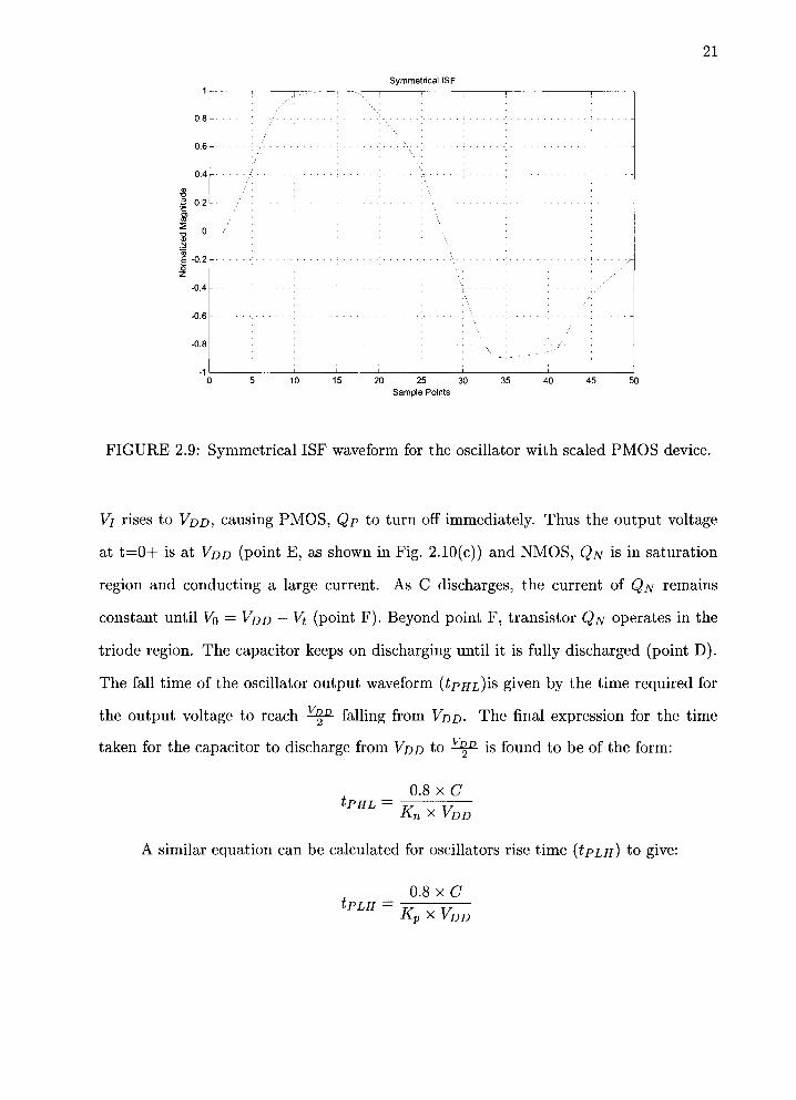
in Fig 29 As can be observed the ISF is symmetrical about zero This is because of
the oscillator having equal rise and fall times
To derive the necessary condition to obtain equal rise and fall times for the ring
oscillator output consider a single stage of a CMOS ring oscillator as shown in Fig 210
It is composed of a PMOS and NMOS device To calculate the rise and fall times of the
output waveform consider an input pulse going from 0 to VDD at time t=O as shown in
Fig 210(a) Assume that just prior to the leading edge of the input pulse (that is at
t=O-) the output voltage equals VDD and capacitor C is charged to this voltage At t =0
21
Symmetrical ISF
08
06
04
C 3 02~c
I
o~ ~ iiE -02
~ -04
-06
-08
-1 0 5 10 15 20 25 30 35 40 45 50
Sample Points
FIGURE 29 Symmetrical ISF waveform for the oscillator with scaled PMOS device
VI rises to VDD causing PMOS Qp to turn off immediately Thus the output voltage
at t=O+ is at VDD (point E as shown in Fig 21O(c)) and NMOS QN is in saturation
region and conducting a large current As C discharges the current of QN remains
constant until Vo = VDD - vt (point F) Beyond point F transistor QN operates in the
triode region The capacitor keeps on discharging until it is fully discharged (point D)
The fall time of the oscillator output waveform (tpHdis given by the time required for
the output voltage to reach V~D falling from VDD The final expression for the time
taken for the capacitor to discharge from VDD to V~D is found to be of the form
08 x C tpHL = K TT
n X VDD
A similar equation can be calculated for oscillators rise time (tPLH) to give
08 x C tpLH = K V
P X DD
22
Voo
Voo ---------~------
(a) (b)
Operating point at t=O+
I
F E Voo
Operating point Operating point after switching is at t=Oshycomplete
AD ~________~____~~______~
o Voo V Voo Vo
(c)
FIGURE 210 (a) Input Waveform (b) Single-stage circuit (c)Trajectory of the output as the input goes high and C discharges through QN
For the oscillator to have symmetric rise and fall edges it is necessary to have equal
rise and fall times ie tpHL = tpLH Therefore
08 x C 08 x C Kn x VDD Kp X VDD
23
For equal length devices we have
- J-lnWnWp- (213) J-lp
Therefore appropriate scaling of PMOS device as given by (213) ensures that the
oscillator output has symmetric rise and fall edges and hence low DC ISF value
27 Calculation of Phase Noise Spectrum for Ring Oscil-lators
If the above criteria for symmetric oscillator output waveform is met then the only
dominant noise source in the ring oscillator circuit is MOSFET white noise Thus the
flicker noise generated by the MOSFET can be safely ignored and the expression for i~
is given by
(~j)Single-Stage (~j)N + (~j)P
Where
(fb)N = and (fb)P = 4kT x gdsP4kT X gdsN (214)
Where gdsN and gdsP are the transconductance of NMOS and PMOS calculated
when the noise is at its maximum ie when Voutput = V~D As the noise sources are
uncorrelated with each other the total noise for an N-stage ring oscillator is given by N
times that for the single-stage Therefore
2 ) 2 )~ =Nx ~ =Nx( (tlj N -Stages tlj Single-Stage
Substituting (215) in (29) the phase noise spectrum for an N-stage ring oscillator is
given by
(215)
00
xLc n=O (216)L(lw) =
24
FIGURE 211 Cadence schematic of 3-stage ring oscillator
00
N x [4kT gdsN + 4kTmiddot gdsP ] x 2= c~ n=O (217)L(tlw) =
According to Parseval s relation
(218)
Giving
L(tlw) = (N x [4kT gdsN 4kT ~dSP] X 2rms) (219)4 x qmax X tlw
L(tlw) = x [4kT 9dSN + 4kT idsP ] x rms ) (N 2 (2 20)
2 x qmax X tlw
28 Comparison of Hajimiri Phase Noise Model with Spec-treRF PSS Phase Noise Analysis
To verify the validity ofHajimiri phase noise model we compared it with SpecterRF
PSS phase noise results which are known to be very accurate Simulation experiments
were performed on ring oscillators of different stages having transistors of different sizes
The schematic of the ring oscillator used in the simulations is as given in Fig 211
25
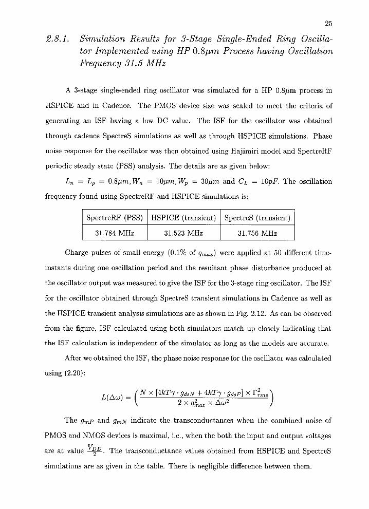
281 Simulation Results for 3-Stage Single-Ended Ring Oscilla-tor Implemented using HP O8-Lm Process having Oscillation Frequency 315 MHz
A 3-stage single-ended ring oscillator was simulated for a HP 08jlm process in
HSPICE and in Cadence The PMOS device size was scaled to meet the criteria of
generating an ISF having a low DC value The ISF for the oscillator was obtained
through cadence SpectreS simulations as well as through HSPICE simulations Phase
noise response for the oscillator was then obtained using Hajimiri model and SpectreRF
periodic steady state (PSS) analysis The details are as given below
Ln = Lp = 08jlm Wn = lOjlm Wp = 30jlm and CL = 10pF The oscillation
frequency found using SpectreRF and HSPICE simulations is
SpectreRF (PSS) HSPICE (transient) SpectreS (transient)
31784 MHz 31523 MHz 31756 MHz
Charge pulses of small energy (01 of qmax) were applied at 50 different time-
instants during one oscillation period and the resultant phase disturbance produced at
the oscillator output was measured to give the ISF for the 3-stage ring oscillator The ISF
for the oscillator obtained through SpectreS transient simulations in Cadence as well as
the HSPICE transient analysis simulations are as shown in Fig 212 As can be observed
from the figure ISF calculated using both simulators match up closely indicating that
the ISF calculation is independent of the simulator as long as the models are accurate
After we obtained the ISF the phase noise response for the oscillator was calculated
using (220)
The gmP and gmN indicate the transconductances when the combined noise of
PMOS and NMOS devices is maximal ie when the both the input and output voltages
are at value V~D The transconductance values obtained from HSPICE and SpectreS
simulations are as given in the table There is negligible difference between them
FIGURE 212 ISF for 3-Stage ring oscillator obtained using SpectreS and HSPICE simulations
SpectreS HSPICE
9mN 9mP 9mN 9mP
1588e-3 2056e-3 1560e-3 212e-3
The phase noise spectrum for the oscillator using SpectreS and HSPICE simulashy
tions is shown in Fig 213 There is no visible difference between the two-phase noise
spectrums and they exactly overlap over each other
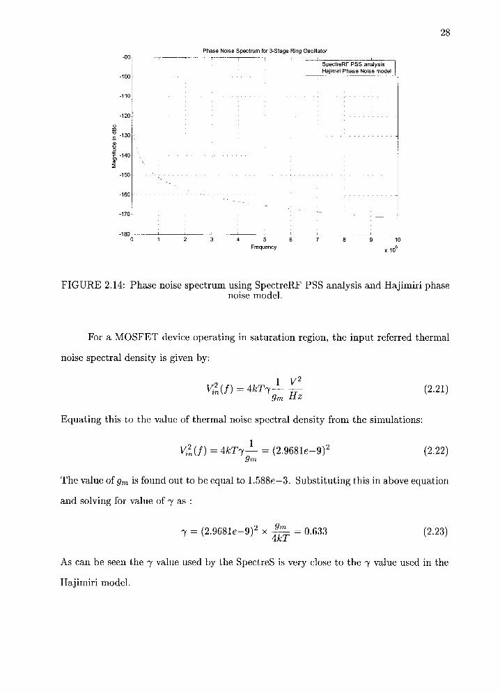
In Fig 214 plots of the phase noise spectrum generated using SpectreRF PSS
phase noise analysis and Hajimiri model phase noise model (ISF generated using HSPICE)
are as shown
The dBc values of phase noise at an offset of 1 MHz for the 2 plots are
SpectreRF (PSS) Hajimiri
-1511 -1512004
As seen from the figure Hajimiri model predicts the phase noise values very close
to values obtained through SpectreRF PSS phase noise analysis The difference between
27
the two was found out to be approximately equal to OldB or 006624 error in dB The
value of I used in Hajimiri model was 23 = 0666 Since I is process dependent further
analysis was performed to determine the I value used by the SpectreRF noise analysis
The circuit used for analysis is as shown in Fig 215
The circuit of Fig 215 was simulated using SpectreS AC noise analysis Since the
noise due to PMOS and NMOS in a single stage of a ring oscillator is maximum when
both in and Vout = 25 V the Vgs = Vds value for the noise analysis performed was
chosen to be 25 V The resistor value is chosen to be 1 mQ so that the voltage drop
across it is negligible and hence value of Vout = Vds ~ 25V The noise generated by
the resistor is turned off and therefore the only noise contributor in the circuit is the
NMOS device The noise analysis was run from frequency 1 kHz to 2 MHz and the input
referred spot noise was found to be 29681e-9 k
Phase Noise Spectrum for 3middotStage Ring Oscillator oo~-------------------------~==~~
I HSPICE I L--------Spec reS----tc--JJ
-100
-110
-1 20
~ -130 pound
-g 1sect -140 ggt
-1 50
-160
-170 -
_180 L-_--____ --__-----_-L_--__L_--__L_-- o 4 6 7 8 9
Frequency
FIGURE 213 Phase noise spectrum plot from Hajimiri phase noise model calculated using ISF obtained from SpectreS and HSPICE simulations
28
Phase Noise Spectrum for 3-Stage Ring Oscillator -90 - ----------------- 1
SpectreRF PSS analysis ~ajimiri Phase Nois~model
-100
-110
-120
u lD
~ -130 Q) 0 J
lsect -140 ggt
-150
-160
-170
J _____ -1 __-180 o 2 3 4 5 6 7 8 9 10
Frequency 6 X 10
FIGURE 214 Phase noise spectrum using SpectreRF PSS analysis and Hajimiri phase noise model
For a MOSFET device operating in saturation region the input referred thermal
noise spectral density is given by
(221 )
Equating this to the value of thermal noise spectral density from the simulations
Vi~ (f) = 4kTY~ = (29681e-9)2 (222)9m
The value of gm is found out to be equal to 1588e-3 Substituting this in above equation
and solving for value ofY as
Y = (29681e-9)2 x Ikr = 0633 (223)
As can be seen the Y value used by the SpectreS is very close to the Y value used in the
Hajimiri model
29
V~lV ~ VdC=2 5V f
25V
NMOS W= lO)lffi L=O8)lffi
V out
FIGURE 215 Thermal noise analysis circuit for HP 08jLm NMOS process
282 Simulation Results for 3-Stage Ring Oscillator using HP O8J-lm Process having Oscillation Frequency 500 MHz
L~ = Lp = 08jLm Wn = 20jLm Wp = 60jLm and CL = 1pF
Oscillation frequency from HSPICE and SpectreRF simulations
SpectreRF (PSS) HSPICE (transient) SpectreS (transient)
500397 MHz 495689 MHz 500001 MHz
The difference in the two phase noise plots at 1MHz offset from the carrier freshy
quency measured in dBc
SpectreRF (PSS) Hajimiri
-13053 -13061
283 Simulation Results for 3-stage Ring Oscillator using HP 12J-lm Process having Oscillation Frequency 154 MHz
Ln = Lp = 12jLm Wn = 20jLm Wp = 60jLm and CL = 1pF
The frequency of oscillation from HSPICE and SpectreRF simulations
SpectreRF (PSS) HSPICE (transient) SpectreS (transient)
154087 MHz 152419 MHz 15384 MHz
30
The phase nOIse plots using SpectreRF PSS phase nOIse analysis and Hajimiri
phase noise model are shown in Fig 217 The difference in the two phase noise plots in
dBc measured at 1 MHz offset is
SpectreRF (PSS) Hajimiri
-13519 -13526
middot70 I-----------
-80 -
-90
g g -120 g ~
-130
-140
-150
-160 --------------shyo 2
Phase Noise Spectrum for 3middotStage Ring Osciliator haling frequnecy = 500MHz -T----- -------------======r=======~==
SpectreRF PSS analysis Hajimiri Phase Noise model
3 4 5 6 7 8 9 10 Frequency
X 10
FIGURE 216 Phase noise spectrum using SpectreRF PSS analysis and Hajimiri phase noise model for 500 MHz oscillation
31
Comparison plot of Phase Noise spectrum for fO =154MHz using 12um process -40
1--sp~ctreRF ~ss P~ase N~ise A~alysis ~jimiri Phase Noise model -50
7 - ~--~-----
-60
-70 -
-80 - ltl III 0 -90shy~
middot5Q)
-100 Z I Q)
~ -110 c a
-120
-130
-140
-150
-160 L __-----_L_----__---
o 2 3 4 5 6 7 8 9 10 Frequency in Hz 6
X 10
FIGURE 217 Phase noise spectrum using SpectreRF PSS analysis and Hajimiri phase noise model for 151 MHz oscillation using HP 12J-lm process
29 MATLAB Graphic User Interface (GUI) for Hajimiri Phase Noise Model
As seen from the previous section the Hajimiri phase noise model is very accurate
for CMOS ring oscillators As a result we developed a MATLAB based Graphic User
Interface(GUI) program to generate the phase noise spectrum for single-ended ring os-
ciIlators using Hajimiri phase noise model The input parameters for the GUI and the
conditions that they need to satisfy are listed in the table below
32
GUI input parameter Condition
Stages The stages entered should be odd
Supply Voltage or Vee (Volts) Vee value should be positive and
lesser than 6V
NMOS Width or Wn(pm) Wn value should be positive and
lesser than lOOOpm
PMOS Width or Wp(pm) Wp value should be positive and
lesser than lOOOpm
NMOS Length or Ln(pm) Ln value should be positive and
lesser than 100pm
PMOS Length or Lp(pm) Lp value should be positive and
lesser than lOOpm
Load Capacitance or C (pF) Capacitance value should be posishy
tive and lesser than 1pF
When the MATLAB GUI program is called it prompts the user for the above input
parameters If the user input violates any condition as specified above for a particular
input parameter then the field is cleared and an error message is displayed informing
the use of the faulty condition After all the correct parameters have been entered the
ISF for the current oscillator configuration can be plotted using the button labeled Run
HSPICE and Plot ISF and Oscillators Expected Frequency Spectrum The flow of the
GUI program is as shown in Fig 218
33
netlist for the Ring Oscillator as per the user specifications and call the
HSP(CE program
HSPICE
3
Simulate the Ring Oscillator circuit and generate the output files containing the oscillation
frequency and (SF
FIGURE 218 MATLAB Graphic User Interface flow diagram
210 Generation of ISF for the User-Specified Ring Oscil-lator
The most accurate method for ISF calculat ion is to replace the noise sources in
the circuit with impulse sources of small energy and then measure the resultant phase-
shift HSPICE simulations were used to obtain the ISF for the ring oscillator using this
method Three HSPICE netlists for each single-ended ring oscillator are generated using
the PERL script isLgeneration according to the user specifications obtained using the
MATLAB Graphic User Interface (GUI) program osc-parametersm
Check the user inputs and then call the PERL
program to get ISF oscillation frequency
and amptsP and gdsN
MATLABGUI
4 Extract the ISF osci llation
frequency amptsP and gdsN from HSPICE output files
2
Generate the HSPICE
Phase No isc spectrum for the cu rrent Singleshyended Ring Oscillator
34
The first net list does not contain any noise elements and is used for calculation of
the oscillation frequency gdsP and gdsN values The HSPICE simulation for this net list is
run first to obtain the oscillation period which is used for defining the transient analysis
and measure statements in the second net list and third netlist The transient analysis
is run for 11ls The oscillation period is measured after a delay of 100 ns under the
assumption that the ring oscillator frequency is atleast 100 MHz and the oscillator has
thus completed more than 10 cycles giving it enough time to settle down The gdsP and
gdsN values are extracted from the DC operating point analysis performed by HSPICE
for this netlist
The second netlist is used to get the time-instants when the oscillator output
voltage crosses half the supply voltage value during 10th and 30th cycles Since there are
no noise sources in this netlist these values represent time-instants for an ideal oscillator
and are used as reference values for ISF calculation in the third netlist
The third net list is generated for calculation of ISF for the ring oscillator It
contains a Piece Wise Linear (PWL) noise current source defined at node1 as shown
in Fig 219 which injects current impulses are at 50 equidistant time instants of the
oscillator period The impulse is applied during the 10th cycle giving enough time for
the oscillator to stabilize and initial transients to die down The impulse causes a time-
shift in the oscillation and hence a phase-shift The analysis is defined as a sweep analysis
to get 50 different oscillator waveforms for 50 different impulses This enables viewing of
effect of each impulse on the oscillator output independently The resultant time-shift
hence phase-shift in the oscillator output is observed after a gap of 20 cycles to allow the
amplitude disturbance in the oscillator to die down As a result the time-shift observed is
solely due to phase disturbance The time-instant when the output voltage of 30th cycle
crosses value Vee 2 is measured and subtracted from the reference value obtained from
simulation of netlist 2 to give the time-shift Since a single oscillator cycle is equivalent
to 3600 or 21f radians phase shift the resultant phase-shift is given by
t cent = OmiddotZZ p d X 21f Radzans (224)
SC2 ator erw
35
Models llsed ()r PMOS NMOS III O5U111
Node 1 Vee Vee Vee
Vout
FIGURE 219 3-Stage single-ended ring oscillator with current impulse
Where bt = time - instantmeasured30thcycle - time - reerence30thcycle
Since all the stages of the ring oscillator are identical the ISF seen from every other
node to the output is a delayed version of the ISF from node 1 Therefore the ISF for
the ring oscillator can be calculated by application of current impulses at a single node
node 1 in this case Although the unit impulse response is desired applying an actual
impulse with area of 1 Coloumb would drive the oscillator deep into non-linear behavior
Therefore the unit impulse response is obtained by applying impulses with areas 01 of
the maximum charge flowing into the capacitor at each node of the ring oscillator given
by qmax = Vee x Cnode and then scaling accordingly The current pulse-magnitude is
taken to be 1 rnA and the rise-time and fall-time of the pulse are taken to be 10 of the
total pulse-width This is illustrated in Fig 220 The phase shift calculated from (224)
is scaled to give the final phase shift due a unit charge applied at time-instant t as
bt cent final = X 27r Radwns (225)
Osczllator Penod X Total charge applzed
This calculation is performed for all the 50 points at which the impulse was applied
to give the ISF The final GUI figure looks as shown in Fig 221 There are two plots shy
one for ISF and other depicting the oscillator phase noise spectrum
36
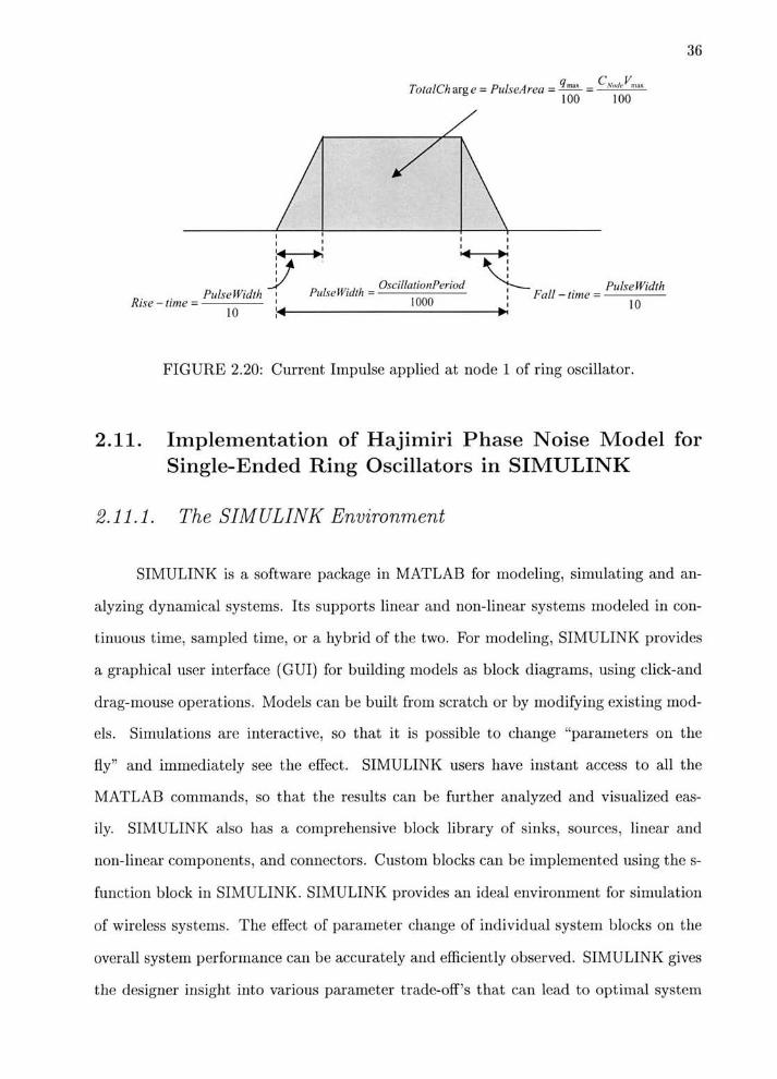
q C VTotalCh arg e =PulseArea =~ = Nod max
100 100
I I
~ ~it L Pulse Width Pulse Width = OscillalionPeriod Fall- time = PulseWidth RIse - time = 1000 10
10 ~r-----------------------~~
FIGURE 220 Current Impulse applied at node 1 of ring oscillator
211 Implementation of Hajimiri Phase Noise Model for Single-Ended Ring Oscillators in SIMULINK
2 111 The SIMULINK Environment
SIMULINK is a software package in MATLAB for modeling simulating and anshy
alyzing dynamical systems Its supports linear and non-linear systems modeled in conshy
tinuous time sampled time or a hybrid of the two For modeling SIMULINK provides
a graphical user interface (GUI) for building models as block diagrams using click-and
drag-mouse operations Models can be built from scratch or by modifying existing modshy
els Simulations are interactive so that it is possible to change parameters on the
fly and immediately see the effect SIMULINK users have instant access to all the
MATLAB commands so that the results can be further analyzed and visualized easshy
ily SIMULINK also has a comprehensive block library of sinks sources linear and
non-linear components and connectors Custom blocks can be implemented using the s-
function block in SIMULINK SIMULINK provides an ideal environment for simulation
of wireless systems The effect of parameter change of individual system blocks on the
overall system performance can be accurately and efficiently observed SIMULINK gives
the designer insight into various parameter trade-offs that can lead to optimal system
37
oscparameters_loadHajDI--- r SIngIe-_ 00cIIalltn
Enter Vee (odd)
Enter No 01 Stages (VoH)
Enter Wn 10 Enter Wp 10 (um) (um)
Enter Lp 10Enter Ln 10 (um)(um)
Enter c 10 (PF)
Run Ibpb amp pIollSF - OocIIalora Expactad Fnqunency Spec I 15Fected Osclllolor Frequenc~ speclrum
FIGURE 221 GUI figure for Hajimiri phase noise model
design The Hajimiri phase noise model for single-ended ring oscillator s is implemented
as a s-function block in SIMULINK
38
2112 Hajimiri Phase Noise Model Implementation in SIMULINK
Using Hajimiris method for ISF calculation the phase disturbance at time instant
t is given by the (22) as
cent(t) = rt f(wor) x i(r)dri-oo qmax
Since the SIMULINK simulation is a discrete-time simulation the continuous-time inteshy
gral has to be replaced by discrete-time summation The above equation is approximated
by
cent(t) = (I r(wok) x i(k)) x lT (226) k=O qmax
Where fo(wok) represents the scaled discrete-time periodic ISF i(k) is the circuit noise
and lT represents the discrete-time step of the simulation which is given by Js where
is represents the sampling frequency used for the simulation
As the ISF used in the summation is 50 points long the sampling frequency is
50 times the oscillator frequency The oscillation frequency for the ring oscillator is
typically between 50 MHz-2 GHz Usually for a system level design SIMULINK simshy
ulations will be carried out with sampling frequency anywhere between 10 kHz to 500
kHz as the simulations are for baseband frequencies Consider the worst-case scenario
where SIMULINK simulation is running at 10 kHz and the oscillator is running at 2
GHz Therefore the time-instants at which the phase disturbance values will have to
be calculated will be multiples of SIMULINK time-step = 101Hz = 01 ms but the ISF
sampling frequency is 2GHz x 50 = 100GHz The summation in (226) has to be carshy
ried out in steps dependent on the ISF sampling frequency ie summation time-steps
= l(fs) = 1(100GHz) = lOps So for each simulation time-step the MATLAB sumshy
mation will have to be carried out over degi6~s = 107 points MATLAB summation over
such a huge number of points requires a lot of memory allocation and processor speed
If adequate resources are not available then this phase noise model block will be the
limiting factor for the SIMULINK simulation speed of the Wireless System
39
2113 Improving the Efficiency of Hajimiri Phase Noise Model Im-plemented in SIMULINK
The MATLAB command randn which generates Gaussian Distributed random
numbers is used to model i(k)- circuit noise in the SIMULINK phase disturbance model
Since the discrete-time ISF is 50 points long the phase disturbance value at the
end of first cycle can be represented by the summation over 50 points given by
M M
fo(l) x randn + fo(2) x randn+L L No of cycles=O No of cycles=Ocent(n) = M
fo(50) x randnL No of cycles=O
(227)
Where M represents the total number of complete oscillation cycles
Since the ISF was composed of 50 points in the above equation are 50 different
summations Now since fo(l) f o(2) fo(50) are constants then each summation term
in the above equation can be written as
M M
Yi= L fo(l) x randn = L (228) Noofcycles=O N oofcycles=O
Where Xi = fi x randn Substituting Yi in (227) the equation for phase disturbance
transforms to
cent(n) = (YI + Y2 + Y3 + + Yso) x In X tT (229)
The value of Yi for a particular value of M is evaluated using statistical results namely
If random variable X is defined as X = Xl + X 2 where Xl and X 2 are independent
random variables having a normal distribution then
1 mean(X) = mean(Xd + mean(X2 )
This applies when Xl and X 2 are independent which they are in each call to
MATLAB function randn
40
2Therefore Yi is a random variable having mean=O and a = r x M This random
variable can be generated in MATLAB using the command randn x r i x VM Reshy
placing Yi in (230) the final equation for calculation of phase perturbation at the end
of M oscillator cycles is given as
cent(n) = (rl x randn + r 2 x randn + r3 x randn + + r 50 x randn) x JM x In X tT
(230)
This equation is computationally efficient Only 50 terms need to be evaluated comshy
pared to M cyclesx50 points in (227) Thus the phase noise model implemented in
SIMULINK is no longer the limiting factor for simulation speed However this method
can only be used for calculating phase disturbances for time-instants which are multiples
of the oscillation period Therefore the calculation of phase disturbance at any arbitrary
instant is divided into two parts - calculation of phase disturbance using the fast method
for complete oscillation cycles that can be accommodated with the time-interval and
then the calculation of phase disturbance during the remaining time-interval for the last
incomplete oscillation cycle This new method developed for implementation of Hajimiri
phase noise model in SIMULINK will be called as fast simulink method
212 Verification of Fast SIMULINK Method for Hajimiri Phase Noise Model Implementation
Before implementing the fast method for Hajimiri phase noise model in SIMULINK
it is necessary to prove that the new technique generates phase disturbance having the
same frequency spectrum as obtained through normal simulation technique for the model
Extensive MATLAB simulations were run to validate the new model using ISFs genershy
ated for different 3-stage ring oscillators
41
2121 MATLAB Test Simulations
MATLAB simulations were run for two different types of ISF generated for 3-stage
ring oscillators - 1) Symmetrical ISF 2) Non-symmetrical ISF Disturbance in oscillators
phase or excess phase of the oscillator is calculated using the original equation as given
by (227) and also using the (230) developed for the fast simulink method All the
calculations for disturbance in phase are performed for complete oscillation cycles The
number of oscillator cycles the simulations are run over is 105 The phase disturbance at
the oscillator output generated using the normal method is sampled every 10 complete
oscillation cycles to give total 104 data points Fast simulink method is then used to
calculate the phase disturbance value every 10th cycle over 105 oscillation cycles giving
another set of 104 data points As data points representing the oscillators disturbance
in phase generated using the two separate methods are for the same oscillator they
can compared with each to establish the validity of the new method MATLABs fft
function is used to get the frequency spectrum for the two sets of readings The FFT
for oscillators phase perturbations generated using the two different methods is averaged
over 1000 such simulations and then compared with each other The results are as given
below
2122 Simulation for Symmetrical [SF
Oscillation
cycles
Sampling
Frequency
FFT points FFT avershy
aged over
Max FFT
value (Orig-
inalFast)
Min FFT
value (Orig-
inalFast)
105 10 104 103 999932
999502
236427
237702
Oscillation
cycles
Mean
(Original)
Mean
(Fast)
Variance
(Original)
Variance
(Fast)
104 -07 -05 16433 16559
42
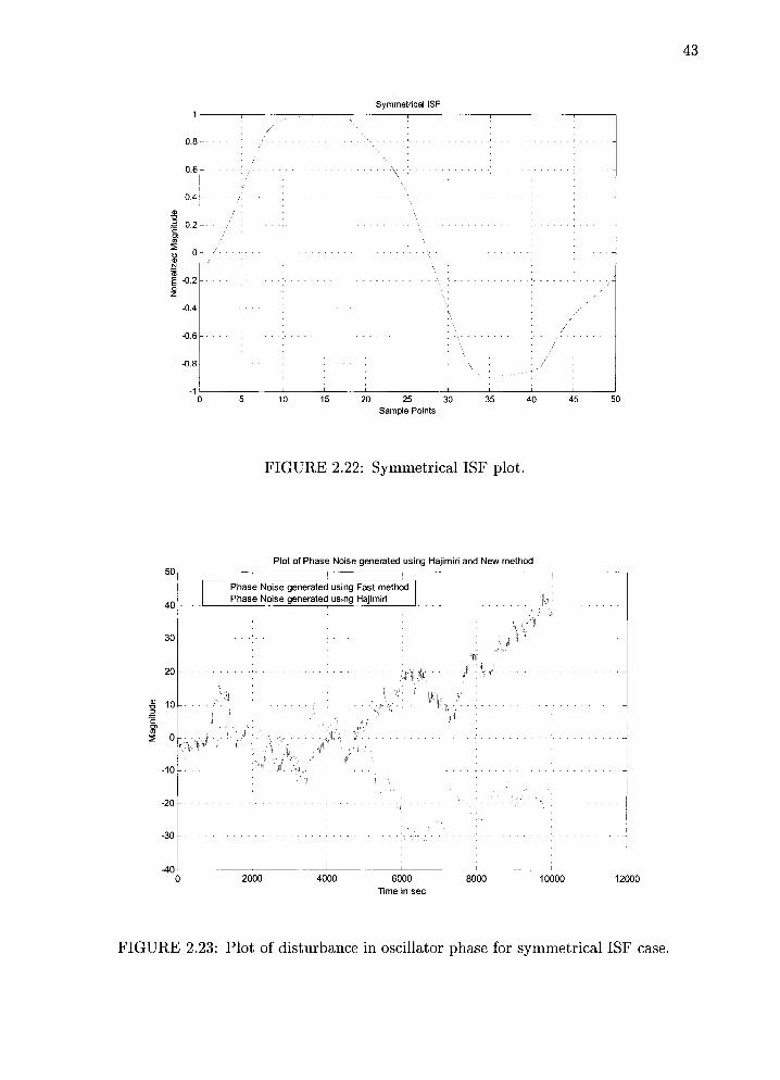
As can be observed from the comparison plot of Fig 224 and the data represented
in the table the phase disturbance generated using the two methods for the ring oscillator
having a symmetrical ISF tally with each other
2123 Simulation for Non-Symmetrical ISF
Oscillation
cycles
Sampling
Frequency
FFT points FFT avershy
aged over
Max FFT
value (Orig-
inalFast)
Min FFT
value (Orig-
inalFast)
105 10 104 103 973064
965318
208774
209542
Oscillation
cycles
Mean
( Original)
Mean
(Fast)
Variance
(Original)
Variance
(Fast)
104 -04679 -03013 17128 17204
43
Symmetrical ISF
08
06
I OAL
0 3 02middot2 Ol co
0aJ ~ mE -02 ~
-004
-06
-08
-1 0 5 10 25 30 35 40 45 50
Sample Points
FIGURE 2_22 Symmetrical ISF plot_
Plot of Phase Noise generated using Hajimiri and New method 50
Phase Noise generated using Fast method Phase Noise generated using Hajimiri
40
30
20
i-0 10 13
ro
-10
-20
-30
-40 0 2000 4000 6000 8000 10000 12000
TIme in sec
FIGURE 223 Plot of disturbance in oscillator phase for symmetrical ISF case
44
Comparison plot of FFT of Phase Noise generated using Hajimiri Method and Fast method O--------r -----------T-------- shy
FFT using Fast method i FFT usingHajimiri I
-10~
-20
-30 ID 0
~ -40 ilmiddot2 ggt -50
-60
-70
~-----~----60 o 05 15 2 25
Frequency in multiples of 1MHz
FIGURE 2_24 Comparison plot of frequency spectrums of phase disturbance generated using the two methods in dBc for symmetrical ISF case
Unsymmetrical ISF 04
02
0
-020 ilmiddot2 Ol -04
-06
-08
-1
0 5 10 15 20 25 30 35 40 45 50 points
FIGURE 225 Non-symmetrical ISF plot
45
Plot of Phase Noise generated using Hajimiri amp New Fast method 40 -~------~====~==~========~~====~
Phase Noise generated using Hajimiri Method Phase Noise generated using Fast Method
30
20
10
Ql0 3
0 OJ
-10
1-
-20
-30
-40 0 2000 4000 6000
TIme in sec 8000 10000 12000
FIGURE 226 Plot of disturbance in oscillator phase for non-symmetrical ISF case
Comparison plot of FFT of Phase Noise generated using Hajimiri amp Fast method
0_--------------~~---~~~======~~---shy[-~ FFT using Hajimiri methOd
FFT using Fast method -10shy
-20
-30 co 0 5 ~ -40
dege ggt -50
-60
-70
-80 o 05 15 2 25
Frequency in multiples of 1MHz
FIGURE 227 Comparison plot of frequency spectrums of phase disturbance generated using the two methods in dBc for non-symmetrical ISF case
46
213 SIMULINK s-Function Implementation of Fast Ha-jimiri Phase Noise Model
From the results presented in the above section it is confirmed that the fast
simulink method for modeling of disturbance in oscillators phase works Therefore we
use it to implement a Hajimiri phase noise model as a s-function block in SIMULINK
An s-function is a SIMULINK descriptor for dynamical system s-functions use
special calling syntax that enables interaction with SIMULINKs equation solver
SIMULINK makes repeated calls during specific stages of simulation to each block in
the model directing it to perform tasks such as computing its outputs updating its
discrete states etc Additional calls are made at the beginning and end of simulation
to perform initialization and termination tasks SIMULINK is real-time simulation enshy
vironment and since the introduced phase disturbance persists indefinitely the value of
phase disturbance calculated in the previous iteration is used as a starting value for the
phase disturbance in the current iteration
The general flow diagram of Hajimiri phase noise model s-function block is as
shown in Fig 228 The fast simulink method developed is used in the s-function to calshy
culate the phase disturbance for complete oscillation cycles during the current time-step
and this value is added to the phase disturbance value calculated for the last incomplete
cycle to give the phase disturbance value at the end of the current time-step
47
Initialize all the outputs to 0 at t = 0
Get the phase disturbance value from previous iteration and use it as the starting value of phase disturbance for the
current iteration
Feedback values
Calculate the phase disturbance for complete oscillation cycles in the current time-step using fast method
Calculate the phase disturbance for the incomplete portion of the last oscillator cycle
Phase disturbance value at the end of current iteration
FIGURE 228 Flow diagram of SIMULINK based fast Hajimiri phase noise model
48
3 IMPLEMENTATION OF PHASE NOISE MODEL USING DIGITAL FILTER
In some cases job of a designer is to choose the right oscillator to optimize the
costperformance ratio of the system To do this it is necessary for the designer to
observe the effect of using different oscillators having different phase noise specifications
on the performance of the whole system The designer may have information about the
phase noise spectrum for the oscillator from the manufacturer or through actual test
measurements To perform system level SNRBER simulations that include the effect
due to phase noise a model that generates phase noise having a spectrum identical to
that specified by the manufacturer or obtained through measurements is needed We
have implemented a system to do this in MATLAB using a white noise generator and
a digital filter The digital filter is implemented as a Finite Impulse Response (FIR)
filter which is designed on the fly using the MATLAB command fir2 As shown in
Fig 31 the user inputs the PSD in dBcHz at several frequency points and the order
of the digital FIR filter
31 Calculating the Phase Disturbance Response from the Oscillators PSD
For system level simulations an important quantity of interest is the phase disshy
turbance This is because the terms sin(cent) and cos(cent) appear in equations for BER of
digital communication systems It is therefore necessary to go through voltage-to-phase
conversion process before designing the digital filter which will model the disturbance in
oscillators phase
As has been discussed before in Section 24 for small values of cent(t) cos(wot+cent(t))
can be approximated as
49
Phase Noise specs for the filter
dB
Highest frequency point F=l
1Hz Frequency
FIGURE 31 Oscillators frequency response
cos (wot + cent(t)) = cos(wot)cos(cent(t)) - sin(wot)sin(cent(t)) ~ cos(wot) - cent(t)sin(wot) (31)
Where it is assumed that cos(cent(t)) ~ 1 and sin(cent(t)) ~ cent(t) for small values of cent(t)
Using this narrowband modulation approximation cent(t) at 6w results in a pair of equal
sidebands as illustrated below
Let cent(t) = XIsin(6wt) be the low frequency fluctuation in phase having power
spectral density = yen at frequency 6w It is represented by one-sided frequency specshy
trum having a peak at H (Dw) = Xl Thus Xl is the spectral value of time function
cent(t) Substituting value of cent (t) in (31)
cos(wot + cent(t)) = cos(wot) - XIsin(6wt) x sin(wot) (32)
Therefore
Xl Xlcos(wot + cent(t)) = cos(wot) - TCos(wO + 6w)t - Tcos(wot - 6w)t (33)
(34)
50
Where Al is the PSD value of the oscillators phase noise spectrum at frequency
offset t1w - which is specified by the user Therefore the PSD of cent(t) is specified by
values which are 2 times the square root of the power spectral density spectrum values
specified by the user and the frequency spectrum of cent(t) is specified by a values given
by 2 X PdBc at different frequency offsets from the carrier frequency
(35)
(36)
Lets consider what happens when the disturbance is at DC Let cent(t) = A Then
substituting value of cent(t) in oscillator output equation Vout = cos(wot+cent(t)) after going
through the approximation for small cent(t) we get
cent(t) ~ cos(wot) - cent(t) x sin(wot) = cos(wot) - A x sin(wot) (37)
The PSD of cent(t) is given by
(38)
As phase noise spectrum is specified in dBc the PSD value at zero frequency offset
from the carrier is 0 dBc and therefore H(O) is 1 The frequency response of the digital
filter for frequency offsets from carrier (t1w) gt 0 is calculated using (36)
MATLAB command fir2(NFM) is then used to design Nth order FIR The
vectors F and M specify the frequency and magnitude breakpoints for the filter as specshy
ified by the user F is normalized to be between 0 to 1 with 1 representing the highest
frequency offset from the carrier as shown in Fig 31 The frequency response of the
FIR filter is obtained using the MATLAB command freqz Since the digital filter is
used to model the oscillators phase disturbance the digital filters frequency response
is equivalent to Hltp(t) (w) Using (36) the relationship between phase noise PSD values
and Hltp(t) (w) is given by
(39)
(39) is used to get a comparison plot of PSDs of the digital filter and phase noise
response for the oscillator specified by the user If the filters PSD response is found to
51
Phase Noise output _ _ D_ig_ita_I_FI_~___Rand_n__~r-__________~~I~___ lt_er~r-__~~~
White Noise FIR Filter Generator
dB dB
o o
dB
o
f f f Frequency Frequency Frequency
FIGURE 32 Generation of oscillators phase disturbance using digital FIR filter
be unsatisfactory then the order of the filter is varied until an acceptable filter frequency
response is obtained
The final SIMULINK model implementation is as shown in Fig 32 White noise
having 0 dB PSD is generated by the random number generator randn which has a
flat PSD The noise is then passed through the digital FIR filter As a result the flat
band frequency response of White noise gets shaped by the filter response to give the
required excess phase output having frequency response similar to that of the spectrum
of oscillators phase disturbance
The power of ltJ(t) at the output of the digital filter is 0 dB at DC and has to
be scaled depending upon the carrier power The output of the digital filter is passed
through a constant source SIMULINK block having magnitude equal to the square-root
of carrier power to give the final phase disturbance values to be used in simulations
52
32 MATLAB GUI Designed for the Design of FIR Filter
The Graphic User Interface developed in MATLAB is used to get the PSD values
for the oscillator spectrum from the user needed to design the FIR filter of user specified
order It then plots the computed PSD and specified PSD for comparison The user
can specify 10 different frequency and dBc values The frequency points entered are in
kHz The GUI checks to see that there is a dBc value for every frequency point entered
and vice-versa The dBc values entered should always be negative and frequency points
should always be positive After correct values are entered the user can select the order
of the filter and then check to see if the filter PSD looks satisfactory If not then the
order of the filter can be changed or more data points may be entered until a satisfactory
filter is designed The final GUI is as illustrated in Fig 33
- ----
53
r- ------ - -~- --------------------------~~~--- ---_=_1
~ Digital Filter Parameters I I
Digital FIR Alter for Phase NoIse generation
Enter the Order of Filler to be desglned
uata 101015 Frequency offset from carrier (KHz) Magnitude of Osciiiator Ouput Voltage (dBc) ---z- -65 ]
-~ 2 ~~ ~o 9 ~- tf- I ic-~t - 62 l
3 5 -60 I 4 ----- rTn l 5 - 2 -4 0
6 3 -
-50
7 05 - 15
0
9 --
0
10 ~
-
Power Spectral DensHy Plot of the Designed dlgHal FIR niter and Osclllalor Phue Nolle spectrum
- Dig ilal FIR Filter - User inputi_
5 g -15 _
c f -20 - Ii
FIGURE 33 MATLAB GUI for digital FIR filter design
54
4 LOCAL OSCILLATOR MODEL IMPLEMENTED IN COMMIC
Communication IC Tool-Box or COMMIC is a simulink based tool-box that can be
used to design communication systems COMMICs focus is to tie system level design
and circuit level design together A typical COMMIC implementation is as shown in
Fig 41
Fig 41 lists only a few blocks of the toolbox The Local Oscillator (LO) block
in COMMIC has been implemented using the fast simulink method explained in secshy
tion 213 and using the digital FIR filter as explained in section 31 To observe the
effect of oscillator phase noise on BER of a digital communication system the quantity
of interest is cos(cent(t)) + j sin(cent(t)) This is generated by the LO block as shown in the
Fig 42
Either Hajimiri phase noise model implementation or digital filter implementation
of the model for disturbance in oscillators phase is selected by double-clicking on the LO
block Selecting either method results in the display of MATLAB GUI for that model
as shown in Figs 43 and 44 After the user input parameters have been entered
Source Block 1-------+1
Source block
1) BPSK 2) OAM 3) Pi4DOPSK 4) BFSK 5) OOPSK 6) GMSK 7) MSK
I Channel I
__ J Mixer Final Output after Demodulation scheme
1) Ring resonator Noisy channel Demodulation 2) Diode Mixer 3) Active Mixers
Bit error rate calculation
Local Oscillator Block
FIGURE 41 Communication IC toolbox
55
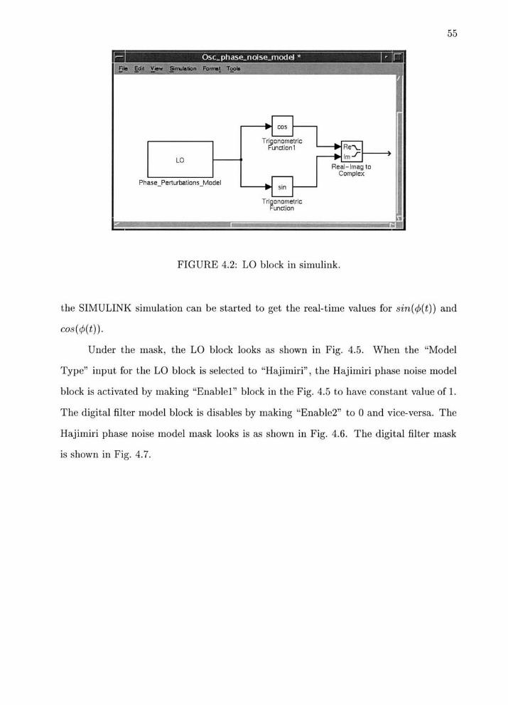
Real-lmag to LO
Complex Phase_Perturbations_Model
Trigo nometri c Function
FIGURE 42 LO block in simulink
the SIMULINK simulation can be started to get the real-time values for sin(cent (t)) and
cos(cent (t ))
Under the mask the LO block looks as shown in Fig 45 When the Model
Type input for the LO block is selected to Hajimiri the Hajimiri phase noise model
block is activated by making Enablel block in the Fig 45 to have constant value of 1
The digital fil ter model block is disables by making Enable2 to 0 and vice-versa The
Hajimiri phase noise model mask looks is as shown in Fig 46 The digital filter mask
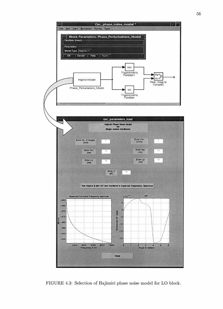
is shown in Fig 4 7
56
---------------shy ~ ----shy -Osc_phase_nolse_modeJ
Hajimiri Model
Phase_Pertllbations_Model
Enter NO of Stagn Entor Vee (odd) (Von)
Entor Wn 10 Entor Wp 10 CUm) (um)
Entor In (um)
10 Entor lp 10
(um)
Entor C (pFJ
_ It tSF OIdIa Expec rnqcy Spectrum I
FIGURE 43 Selection of Hajimiri phase noise model for LO block
57
Digital Filter
Phase Perturbations_Model
Tri~~~~~~trlc
FIGURE 44 Selection of digital filter model for LO block
- -
58
~- -~
- Oscphase_nolse_modeJlPhase Perturbatlons_ModeJ _so ~ _ middottw400~ 1 l - l~ ~_4gtlaquo ~_ ~ gt ~- t _ _ JYih~i ~ _JO
Hajimiri Model for Phase Noise in Single-ended Ring Oscillators
Enable 1
Enable2
FIGURE 45 Mask of LO model
signal1 signal2 signal3rt Hsigna14
- ~ 1I I Ollsimu5 DemlD(r lshy1 S-FlJ1dion
FIGURE 46 Hajimiri phase nOIse model mask
59
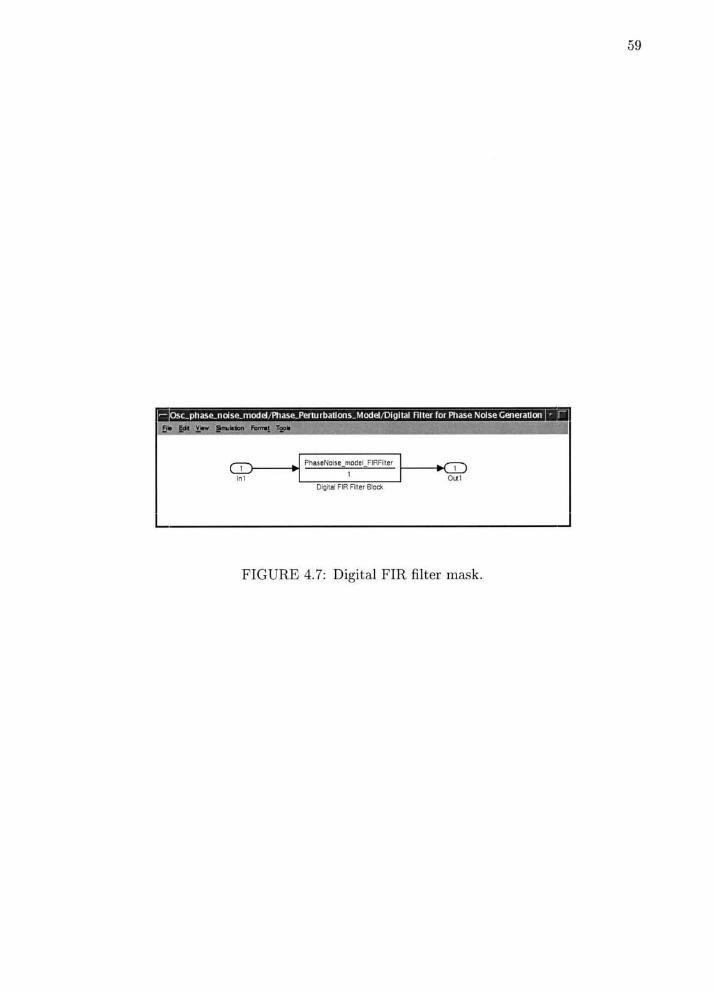
)----+1 PhaseNoise model FIRRlter
Digital FIR Fi~er Block
FIGURE 47 Digital FIR filter mask
60
5 CONCLUSIONS
1 Hajimiri phase noise model for single-ended ring oscillators is accurate
2 The Hajimiri phase noise model s-function block implemented in MATLABs
SIMULINK environment using the fast algorithm is accurate and efficient
3 The digital FIR filter block implemented in SIMULINK can used to model the
oscillator phase disturbance accurately
4 The LO s-function block implemented in SIMULINK is capable of generating phase
disturbance values accurately using either Hajimiri phase noise model or digital
FIR filter
5 The LO s-function block can be used in SIMULINK simulations for communication
systems
61
BIBLIOGRAPHY
1 Behzad Razavi A study of phase noise in cmos oscillators IEEE JSSC 31(3)331~ 343 1996
2 DB Leeson A simple model of feedback oscillator noise spectrum Proceedings of IEEE 54(2) 329~330 1966
3 Asad A Abidi Analog Circuit Design Rf Analog-To-Digital Converters Sensor and Actuator Interfaces Low-Noise Oscillators Plls and Synthesizers Chapter 4 How Phase Noise Appears in Oscillators Kluwer Academic Publications 1997
4 Wang HongMo A Hajimiri and T H Lee Design issues in cmos differential Ie oscillators IEEE JSSC 35(2)286~287 2000
5 Ali Hajimiri and Thomas H Lee A general theory of phase noise in electrical oscillators IEEE JSSC 33(2)179~194 1998
6 S Limotyrakis Ali Hajimiri and Thomas H Lee Jitter and phase noise in ring oscillators IEEE JSSC 34(6)790~804 1999
7 Ali Hajimiri Jitter and phase noise in electrical oscillators Special University Oral Examination April 8 1998
8 Ali Hajimiri and Thomas H Lee Corrections to a general theory of phase noise in electrical oscillators IEEE JSSC 33(6)928 1998
9 Theodore S Rappaport Wireless Communications Principles and Practice Prenshytice Hall 1995
10 Couch II Leon W Digital and Analog Communication Systems Prentice Hall 1995
11 John G Proakis and Dimitris G Manolakis Digital Signal Processing Principles Algorithms and Applications Prentice Hall 1995
12 Behzad Razavi RF Microelectronics Prentice Hall 1997
13 Behzad Razavi Design of Analog CMOS Integrated Circuits McGraw Hill College Division 2000
14 Thomas H Lee The Design of CMOS Radio-Frequency Integrated Circuits Camshybridge University Press 1998
15 David A Johns and Ken Martin Analog Integrated Circuit Design John Wiley amp Sons 1996
16 BP Lathi Modern Digital and Analog Communication Systems Oxford University Press 1998
62
17 Adel S Sedra and Kenneth C Smith Microelectronic Circuits Oxford University Press 1998
18 Bernard Sklar Digital Communications Fundamentals and Applications Prentice Hall 1988
19 Thomas H Lee and Ali Hajimiri Oscillator phase noise A tutorial IEEE JSSC 35(3)326-336 2000
20 Ali Hajimiri and Thomas H Lee Phase noise in cmos differential Ie oscillators Symposium on VLSI Circuits June 11-13 1998 Honolulu Hawaii
21 Ali Hajimiri S Limotyrakis and Thomas H Lee Phase noise in multi-gigahertz cmos ring oscillators Custom Integrated Circuits Conference May 11-14 1998 Santa Clara California
22 Ali Hajimiri and Thomas H Lee Design issues in cmos differential Ie oscillators IEEE JSSC 3(5)717-724 1999

copyCopyright by Devavrata Godbole
October 3 2000
All rights reserved
PHASE NOISE MODELS FOR SINGLE-ENDED RING OSCILLATORS
by
Devavrata Godbole
A THESIS
submitted to
Oregon State University
in partial fulfillment of the requirements for the
degree of
Master of Science
Presented October 3 2000 Commencement June 2001
Master of Science thesis of Devavrata Godbole presented on October 3 2000
APPROVED
Major Pr essor representmg Electncal amp Computer Engmeermg
of Electrical amp Computer Engineering
I understand that my thesis will become part of the permanent collection of Oregon State University libraries My signature below authorizes release of my thesis to any reader upon request
Devavrata Godbole Author
Redacted for Privacy
Redacted for Privacy
Redacted for Privacy
Redacted for Privacy
ACKNOWLEDGMENT
I would like to express my deepest appreciation and thanks to my thesis advisor
Prof John T Stonick for his great enthusiasm in research and invaluable guidance during
my research His passion for teaching and learning has always been a great source of
inspiration for me My appreciation also reaches friends and colleagues I have got to
know during these two years This thesis would not have been completed without their
continuous help and moral support Finally and most importantly I want to express
my sincerest gratitude to my dearest parents for always being there for me No amount
of thanks would be too much for their constant love encouragement and support
dedicate this thesis to them
I
TABLE OF CONTENTS
Page
1 INTRODUCTION 1
11 Definition of Phase Noise and Jitter in Oscillators 1
111 What is Phase Noise 1 112 Units of Oscillator Phase Noise 2 113 What is Jitter 3
12 Importance of Phase Noise Specifications for Communication Systems 4
13 Advantages of Ring Oscillators 6
14 Problem Statement 7
2 HAJIMIRI PHASE NOISE MODEL 10
21 Salient Features 10
22 Explanation 10
23 Conversion of Device Noise to Phase Fluctuations 13
24 Phase-to-Voltage Transformation 16
25 Conversion of Ring Oscillator Device Noise to Phase Noise 16
26 Reducing the Effect of Flicker Noise on Oscillator Phase Noise 19
27 Calculation of Phase Noise Spectrum for Ring Oscillators 23
28 Comparison of Hajimiri Phase Noise Model with SpectreRF PSS Phase Noise Analysis 24
281 Simulation Results for 3-Stage Single-Ended Ring Oscillator Implemented using HP 08J-lm Process having Oscillation Freshyquency 315 MHz 25
282 Simulation Results for 3-Stage Ring Oscillator using HP 08J-lm Process having Oscillation Frequency 500 MHz 29
283 Simulation Results for 3-stage Ring Oscillator using HP 12J-lm Process having Oscillation Frequency 154 MHz 29
29 MATLAB Graphic User Interface (GUI) for Hajimiri Phase Noise Model 31
TABLE OF CONTENTS (Continued)
Page
210 Generation of ISF for the User-Specified Ring Oscillator 33
211 Implementation of Hajimiri Phase Noise Model for Single-Ended Ring Oscillators in SIMULINK 36
2111The SIMULINK Environment 36 2112Hajimiri Phase Noise Model Implementation in SIMULINK 38 2113Improving the Efficiency of Hajimiri Phase Noise Model Impleshy
mented in SIMULINK 39
212 Verification of Fast SIMULINK Method for Hajimiri Phase Noise Model Implementation 40
2121MATLAB Test Simulations 41 2122Simulation for Symmetrical ISF 41 2123Simulation for Non-Symmetrical ISF 42
213 SIMULINK s-Function Implementation of Fast Hajimiri Phase Noise Model 46
3 IMPLEMENTATION OF PHASE NOISE MODEL USING DIGITAL FILshyTER 48
31 Calculating the Phase Disturbance Response from the Oscillators PSD 48
32 MATLAB GUI Designed for the Design of FIR Filter 52
4 LOCAL OSCILLATOR MODEL IMPLEMENTED IN COMMIC 54
5 CONCLUSIONS 60
BIBLIOGRAPHy 61
LIST OF FIGURES
Figure Page
11 Frequency spectrum of an ideal sinusoidal oscillator 1
12 Frequency spectrum of a sinusoidal oscillator having phase noise 2
13 Phase noise measurement 3
14 Jitter 3
15 PLL system 4
16 Generic transreceiver 5
17 Ideal case 6
18 Effect of phase noise on the receive path 8
19 Effect of phase noise on the transmit path 9
110 LC oscillator 9
21 Phase and amplitude response model 11
22 (a) Ideal LC oscillator (b) Impulse injected at the peak (c) Impulse at zero crossing 12
23 Conversion of input noise to output phase noise 13
24 ISF decomposition 14
25 Current noise conversion to excess phase 15
26 Noise in MOSFET 16
27 Conversion of MOSFET device noise to phase disturbance and then to phase noise sidebands 18
28 Non-symmetrical ISF waveform for the oscillator having non-symmetrical rise and fall times 20
29 Symmetrical ISF waveform for the oscillator with scaled PMOS device 21
210 (a) Input Waveform (b) Single-stage circuit (c) Trajectory of the outshyput as the input goes high and C discharges through QN 22
211 Cadence schematic of 3-stage ring oscillator 24
LIST OF FIGURES (Continued)
Figure
212 ISF for 3-Stage ring oscillator obtained using SpectreS and HSPICE simulations 26
213 Phase noise spectrum plot from Hajimiri phase noise model calculated using ISF obtained from SpectreS and HSPICE simulations 27
214 Phase noise spectrum using SpectreRF PSS analysis and Hajimiri phase noise model 28
215 Thermal noise analysis circuit for HP 08J-lm NMOS process 29
216 Phase noise spectrum using SpectreRF PSS analysis and Hajimiri phase noise model for 500 MHz oscillation 30
217 Phase noise spectrum using SpectreRF PSS analysis and Hajimiri phase noise model for 151 MHz oscillation using HP 12J-lm process 31
218 MATLAB Graphic User Interface flow diagram 33
219 3-Stage single-ended ring oscillator with current impulse 35
220 Current Impulse applied at node 1 of ring oscillator 36
221 GUI figure for Hajimiri phase noise model 37
222 Symmetrical ISF plot 43
223 Plot of disturbance in oscillator phase for symmetrical ISF case 43
224 Comparison plot of frequency spectrums of phase disturbance genershyated using the two methods in dBc for symmetrical ISF case 44
225 Non-symmetrical ISF plot 44
226 Plot of disturbance in oscillator phase for non-symmetrical ISF case 45
227 Comparison plot of frequency spectrums of phase disturbance genershyated using the two methods in dBc for non-symmetrical ISF case 45
228 Flow diagram of SIMULINK based fast Hajimiri phase noise model 47
31 Oscillators frequency response 49
32 Generation of oscillators phase disturbance using digital FIR filter 51
33 MATLAB GUI for digital FIR filter design 53
LIST OF FIGURES (Continued)
Figure Page
41 Communication IC toolbox 54
42 LO block in simulink 55
43 Selection of Hajimiri phase noise model for LO block 56
44 Selection of digital filter model for LO block 57
45 Mask of LO model 58
46 Hajimiri phase noise model mask 58
47 Digital FIR filter mask 59
PHASE NOISE MODELS FOR SINGLE-ENDED RING OSCILLATORS
1 INTRODUCTION
11 Definition of Phase Noise and Jitter in Oscillators
111 What is Phase Noise
The output of an ideal oscillator with no noise can be expressed as
VLOoutput = Af[wet + cent]
where A is the peak amplitude of the oscillator We is the oscillator frequency and f the
oscillator phase Note that in the case of an ideal oscillator A We and f are all constants
The one-sided frequency of such an ideal oscillator looks as in Fig 11
However in a practical oscillator due to the presence of noise the output is given
by
VLOoutput = A(t)J[wet + cent(t)]
where A(t) and cent(t) represent the fluctuations in peak amplitude and phase of the
oscillator output and are no longer constants As a consequence of the fluctuations in
oscillators phase and amplitude the spectrum of a practical oscillator has skirts close
Frequency
FIGURE 11 Frequency spectrum of an ideal sinusoidal oscillator
2
Frequency
FIGURE 12 Frequency spectrum of a sinusoidal oscillator having phase noise
to the oscillation frequency as shown in Fig 12 The effects of amplitude fluctuations
in an oscillator are generally reduced by some kind of amplitude limiting mechanism
but the phase fluctuations persist indefinitely Therefore the oscillators spectrum is
mainly dominated by the phase fluctuations and as a result an oscillator spectrum having
sidebands as shown in Fig 12 is generally referred to as the phase noise spectrum
112 Units of Oscillator Phase Noise
Conventional units for expressing oscillator phase noise are decibels below the
carrier per Hertz (dBcHz)
~) 10 I Psideband(WO + ~w 1Hz)P PhaseNoise ( W = x og n (11 ) TCarrler
Where Psideband(WO + ~w 1Hz) represents the single sideband power in the oscilshy
lator spectrum at a frequency offset ~w from the carrier The measurement bandwidth
for the sideband power is 1 Hz as shown in Fig 13
3
dB
1Hz Frequency
FIGURE 13 Phase noise measurement
113 What lS Jitter
Fluctuations in amplitude and phase result in uncertainties in the transition inshy
stants of an oscillators periodic time domain waveform Jitter is defined as the time
deviation of a controlled edge from its normal position
There are several ways in which jitter can be measured Two of the most commonly
used measurements of oscillator jitter performance are
1 Absolute or total jitter (OT) It is a measure of clock jitter relative to its source
at various points along a path which the clock travels as it is affected by various
electronic components It is expressed in units of time usually pico-seconds For
a free running oscillator the total clock jitter increases with the measurement
Unit Sometimes the edge Interval is here
Reference I Edg
------y-r r 1 ICI I I I I I I I I I I I I I I I I I I I I I I I I I I I I I I I I I I I I I
The edges should Somotim (hoodgo ~ ~---=- be here
is here
FIGURE 14 Jitter
4
PLL 1 bullI__P_L_L_2_--
FIGURE 15 PLL system
time-interval This growth in variance occurs because the effect due to phase
disturbances persists indefinitely Therefore the absolute jitter value at time t
seconds includes the jitter effects associated with all the previous transitions
2 Cycle-to-Cycle Jitter It is the instantaneous difference of periods between adjashy
cent oscillator cycles This type of jitter is most difficult to measure and requires
special instrumentation such as timing interval analyzer and other analysis softshy
ware Cycle-to-Cycle jitter estimate is often useful in case of system as shown in
Fig 15 The output of PLLI is the reference for PLL2 If PLL2 cannot lock to
the reference frequency then the cycle-to-cycle jitter measurement of PLLI will
indicate the maximum jitter allowable for PLL2 to lock
12 Importance of Phase Noise Specifications for Commu-nication Systems
In wireless communications frequency spectrum is a valuable commodity Commushy
nications transceivers rely heavily on frequency conversion using local oscillators (LOs)
and therefore the spectral purity of the oscillators in both the transmitter and receiver
is one of the factors limiting the maximum number of available channels and users The
great interest in integrating complete communications systems on a single chip has led
to a new environment for oscillators which has not been explored before To understand
the importance of phase noise in wireless communication systems consider a generic
transceiver shown below in Fig 16 The receiver consists of a low noise amplifier a
band-pass filter and a downconversion mixer The transmitter comprises an upconvershy
5
Low Noise Amplifier
Duplexer Filter
Band-Pass Filter
Local Oscillator (LO)
Power Amplifier
Band-Pass Filter
FIGURE 16 Generic transreceiver
sion mixer a band-pass filter and a power amplifier The local oscillator provides the
carrier signal for both the transmitter and the receiver If the LO contains phase noise
then both the upcoverted and the downconverted signals are corrupted
Referring to Fig 17 we note that in the ideal case the signal band of interest in
frequency domain is convolved with an impulse and thus translated to a lower frequency
and a higher frequency with no change in its shape In reality however the desired
signal may be accompanied by a large interferer in an adjacent channel and the local
oscillator exhibits finite phase noise When the desired signal and the interferer are
mixed with the LO output as shown in Fig 18 the downconverted band consists of
two overlapping spectra The result is that the desired signal suffers from significant
noise due to the tail of the interferer Here the end portions of the interferers frequency
spectrum which leak into the adjacent channels have been referred to as the tails of the
interferer This effect is called as reciprocal mixing
As shown in Fig 19 the effect of phase noise on the transmit path is slightly
different Suppose a noiseless receiver is to detect a signal at W2 from a weak transmitter
while a nearby powerful transmitter generates a signal at WI with substantial phase noise
Then the phase noise tail of the transmitter corrupts the desired weak transmitters
6
t Signal Band (J)
LO
(J)
t Downconverted (J)
Band
FIGURE 17 Ideal case
signal or it can even completely swamp out the weak transmitters signal The difference
between WI and W2 can be as small as a 200 kHz as in G8M while each of these frequencies
is around 900 MHz or 19 GHz Therefore the output spectrum ofLO must be extremely
sharp In the North American Digital Cellular Standard (NADC) 1854 system the phase
noise power per unit bandwidth must be 115 dB below the carrier power at an offset of
60 kHz from the carrier
13 Advantages of Ring Oscillators
Stringent requirements as mentioned above can be met through the use of LC
oscillators Fig 110 shows an example where a transconductance amplifier with positive
feedback establishes a negative resistance to cancel the loss in the tank and a varactor
diode provides the frequency tuning capability The circuit has a number of drawbacks
for monolithic implementation as follows
1 Both the control and the output signals are single-ended making the circuit senshy
sitive to supply and substrate noise
7
2 The inductor Q in a LC oscillator circuit determines how accurately the oscillator
can tune to certain oscillation frequency As a result the inductor (and varactor)
Q required in low phase noise oscillators is typically greater than 20 prohibiting
the use of integrated inductors as it is not possible to get a Q value greater than
10 for monolithically implemented varactors using the current process technology
Ring oscillators on the other hand require no external components and can be
realized in fully differential form but their phase noise tends to be high because they
lack passive resonant elements Therefore there is huge amount of interest to include
ring oscillators in communications systems but to be able to optimize parameters of
communication systems having ring oscillators it is necessary to have ring oscillator
phase noise models that are accurate at circuit level
14 Problem Statement
It is difficult to analyze the effect of phase noise on the performance of communicashy
tion systems Thus a good system level model that can be used in simulation is desired
In this thesis two different models for generation of phase noise are implemented in
MATLABs SIMULINK environment They are
1 Hajimiri Phase Noise model
2 Digital FIR Filter model
Each of these methods is discussed in detail in the following chapters
8
Actual Case
Wanted UnwantedSignal Signal
t 1--
Downconverted Signals
FIGURE 18 Effect of phase noise on the receive path
9
CD ~ 20 Q) Transmitter Phase Noise
C
~ c 0Q)
E E -20 Adjacent Channel Users u Q)
Co (f)
-40 ~ I0 (L
-60
-80 01 02 03 04 05 4
Frequency
FIGURE 19 Effect of phase noise on the transmit path
Frequency _~II1r-- control
C
YOU
FIGURE 110 LC oscillator
10
2 HAJIMIRI PHASE NOISE MODEL
21 Salient Features
There are many models for predicting the phase noise generated in oscillators
[1 2 3 4] Some models are based on time-domain treatments while others like Leeson
model and that proposed by Razavi use a frequency-domain approach to derive a linear
time-invariant models to describe oscillator phase noise
In contrast to the above models the Hajimiri phase noise model uses a linear
time-variant approach for predicting oscillator phase noise Some of its salient features
are
1 It is a physical model that maps electrical noise sources such as device noise to
phase noise It is possible to implement this transistor level accurate phase noise
model in MATLAB for fast and accurate system level phase noise simulations
2 Models implemented at circuit level are slow as simulations take a long time This
is a fast system level model
22 Explanation
For each noise input the disturbance in the amplitude and phase of the oscillator
can be studied by characterizing the behavior of two separate time-variant single-input
single-output systems as shown in Fig 21 As explained in [5] consider the case of an
ideal LC oscillator as shown in Fig 22(a) If an impulse of current is injected at the
time-instant when the oscillators output voltage is at its peak the tank voltage changes
instantaneously as shown in Fig 22(b) resulting in an amplitude change but there is
no change in phase of the oscillator output However application of impulse at the zero
crossing results in some phase-shift but it has minimal effect on the amplitude as shown
in Fig 22(c) It can thus be seen that the resultant change in A(t) and cent(t) in an
11
i(t) ltp(t)
ltp(t)i(t) I -----l~~ hltlgt(tt) ~
o o t
i(t) A(t
A(t)
~
o o t
FIGURE 21 Phase and amplitude response model
oscillator due to noise are time-dependent This is essentially because an oscillator is a
time-variant system
The disturbances in oscillators amplitude die down due to some form of amplitude
restoring mechanism such as automatic gain control (AGe) or due the intrinsic nonshy
linearity of the devices However the excess phase fluctuations do not encounter any
form of restoring mechanism and therefore persist indefinitely For a small area of the
current impulse (injected charge) the resultant phase shift is proportional to the voltage
change 6V and hence to the injected charge 6q Therefore 6rjJ is given by
(21)
The necessary condition for the above equation to hold is 6q laquoqmax Where qmax =
Cnode X Vmax is the maximum charge swing with Vmax being the maximum voltage
swing across the capacitor Cnode where the charge is being injected V max or Vswing is
approximately equal to the supply voltage Vdd in the case of single-ended ring oscillators
The function f(WOT) is the time varying proportionality factor and is called the impulse
sensitivity function (ISF) since it determines the sensitivity of the oscillator to an impulse
input It is a dimensionless amplitude-independent function periodic in 21f that describes
12
(a)
Erfeelor impul slt applied allh e f ern Cllt bsil1g
Phase7H-- shift i
05 r
v 1 r
-05
j
I middot 1
L-~~_~~_~~~_~~------J o 02 0_ 011 2
L ---- 2 ~ I 2 -----~ 1- 1808 -150 O~ 04------cO6--08-~-- 4 ~6 ~=----bull o~
(b) (c)
FIGURE 22 (a) Ideal LC oscillator (b) Impulse injected at the peak (c) Impulse at zero crossing
how much phase shift results from applying a unit impulse at any point in time The
total phase error at any time-instant t is given by the summation of the all the phase
disturbances that have occurred upto that time-instant because the disturbance in phase
is permanent As a result the equation for oscillator phase disturbance in continuous
time domain is given by [6)
(22)
i(t) represents the input noise current injected into the node of the interest The output
voltage V(t) is related to the phase cent(t) calculated in (22) through a phase modulation
process Thus the complete process through which a noise input becomes a output
perturbation in V(t) can be summarized in the block diagram of Fig23 The complete
process can thus be viewed as a cascade of a LTV system that converts current to phase
with a non-linear system that converts phase to voltage
--
13
f(~t) Ideal integration Phase modulation i(t)
qmax
X t
f ltp (t)
Cos(~t + ltp(t)) V (t)
-00
FIGURE 23 Conversion of input noise to output phase noise
Since the ISF is periodic it can be expanded in a Fourier series as [5]
00
Co f(wot) = 2 +~ COS (nwOT + en) n=l
Where Cn are real valued and en is the phase of the nth harmonic en is not important
in the case of random input noise and is thus neglected here Using the expansion for
f(wot) in the superposition integral and exchanging the order of summation and integral
(23)
The above equation identifies individual contributions of the total cent(t) for an
arbitrary input current i( t) injected into any circuit node in terms of the various Fourier
coefficients of the ISF The equivalent block diagram [7] is shown in Fig 24
Each branch acts as a downconverter and a lowpass filter tuned to an integer
multiple of the oscillator frequency For example the second branch weights the input by
q multiplies it with a tone at Wo and integrates the product As can be seen components
of perturbation in the vicinity of integer multiples of the oscillation frequency play the
most important role in determining cent(t)
23 Conversion of Device Noise to Phase Fluctuations
It is essential to see the effect of small sinusoidal to get an idea of how the various
noise sources affect the oscillator Consider a low frequency sinusoidal perturbation
current i(t) injected into the oscillator at a frequency of t1w laquo Wo i(t) = Iocos(t1wt)
14
Ideal integration
t
f CI Cos(~t +ell
t
f bull
bull bull CnCos(n~t +en)
Phase modulation
i(t) v (t) qmax Cos(~t + ~(t))
FIGURE 24 ISF decomposition
The phase disturbance value is given by (23) as
(24)
The arguments of all the integrals in the above equation are at frequencies higher
than 6w and are significantly attenuated by the averaging nature of the integration
except the term arising from the first integral involving Co Therefore cent(t) is given by [5]
loco locojt cent(t) = -- cos(6wT)dT = 6 szn(6wt) (25) 2qmax -00 2qmax w
As a result there will be an impulse at 6w in the one-sided power spectral density
plot of cent(t) as shown in Fig 25 Now consider a current at a frequency close to the
oscillation frequency given by i(t) = hcos((wo + 6w)t)
15
[(01)
I I I I I I I I
~O1 ~O1 I-- I
I I I I
0
Co
S(o1) ) 010
I I I I I I I
~O1 I
--I I I I I
2x01o
C
CJ
I I I I I I I I I
~O1 I
--I I I I I
3x01o
o ~o1 (J)
FIGURE 25 Current noise conversion to excess phase
Again going through the integration for cent(t) we find that now all the integration
term except the term arising from Cl get attenuated resulting in two impulses at +~w
and -~w in the power spectral density plot of cent(t) cent(t) is now given by
hCl cent(t) = ~ sm(~wt)2qmax w
More generally applying current i(t) = In cos ((nwo +~w)t) close to at any integer
multiple of oscillation frequency will result in sideband at +~w and -~w in Scent(w)
Therefore in general cent(t) is given by [5J
cent(t) = Incn
~ sm(~wt)2qmax w
(26)
16
in 2(W) Jj
I iNoise
Thennal Noi se
lo lo lOlo - - ~
loo 2xWo 3xWo w
FIGURE 26 Noise in MOSFET
24 Phase-to-Voltage Transformation
Computation of power spectral density of the oscillator output voltage requires
conversion of excess phase variations calculated in (26) to output voltage The oscillator
output can be expressed as cos(wot + cent(t)) For small values of cent(t) cos(wot + cent(t))
can be approximated as
eos(wot + cent(t)) = eos(wot)eos(cent(t)) - sin(wot)sin(cent(t)) ~ cos(wot) - cent(t)sin(wot)
Where it is assumed that eos (cent(t)) ~ 1 and sin(cent(t)) ~ cent(t)for small values of cent(t)
Therefore substituting cent(t) from (2 6) we get the expression for PSD of the oscillator
output voltage in dBc as [5J
2In X en PdBc(bW) = ( 4 b )
(2 7) x qmax X W
25 Conversion of Ring Oscillator Device Noise to Phase Noise
The circuit noise in CMOS Ring Oscillator is dominated by the fl icker noise and
thermal noise of MOSFET devices The noise power spectral density spectrum typically
looks as shown in Fig 26
17
Flicker noise dominates at low frequencies and usually falls at -10 dBdecade as
its spectral density is inversely proportional to frequency MOSFET thermal noise or
white noise has a constant spectral density over all frequencies and dominates at higher
frequencies The intersection of J and white noise curves is often called as the J noise
corner Now just as explained for a single frequency current source the low frequency
noise band ~w around DC is influenced by Co term in the integration for cent(t) in (23)
It appears as noise band at ~w in spectrum for phase disturbance Similarly noise band
at ~wo + ~w is influenced by Cl and is downconverted to band at ~w However noise
at ~wo - ~w is also influenced by Cl and results in band at ~w Therefore twice the
power spectral density of cent(t) from (27) should be considered to take into account the
contributions due noise at both the frequency bands ~wo - ~w and ~wo + ~w [8]
Therefore the total single-sideband phase noise spectral density due to one noise source
at an offset frequency of ~w is given by the sum of powers of all the components as
shown in Fig 27 and the final expression is given by
(28)L(~w) =
In the above expression In represents the peak amplitude of the noise voltage It
is convenient to express noise in terms of its power spectral density rather than peak [2 2
amplitude Therefore substituting 2 = -lJ where t6f = 1 gives
(29)L(~w) =
18
1 middot 2 ( ) fNoise
Thermal Noise In ill
1f 6w ~ I I I I
w
Co
S~(w)
o 6w w
PM
Sv(w)
FIGURE 27 Conversion of MOSFET device noise to phase disturbance and then to phase noise sidebands
19
26 Reducing the Effect of Flicker Noise on Oscillator Phase Noise
MOSFET device noise in the 1- region can be described by the equation
Where w1- is the corner frequency of the MOSFET 1- noise The resultant phase
noise spectrum due to this 1- noise is given by
(210)
Thus 1- noise gets converted to p in the oscillators phase noise frequency spectrum
and the frequency at which the white noise power equals the sideband power of noise
arising from 1- noise is termed as the p corner frequency (bwp) Solving for bwp
results in following expression for the p corner frequency of the phase noise spectrum
[5]
1 1 ( Co )2 (211)bw j3 = bwy x J2 f rms
Thus the magnitude of noise in the p region of the oscillator spectrum arising
due to MOSFET flicker noise is smaller by a factor equal to c6fms where Co is the DC
value of ISF given by
1 127rCo = - f(x)dx (212)21f 0
Therefore to reduce the effect of flicker noise on the phase noise spectrum it is
necessary to reduce the DC value of ISF Consider ISFs for two different 3-stage ring
oscillators They have the same frequency load capacitance and NMOS devices The
difference is between the width of PMOS devices used in the ring oscillators The
length and width of PMOS device used the first ring oscillator is equal to that of the
NMOS device The ISF for this oscillator is as shown in Fig 28 It has taller and
wider negative lobe than the positive lobe which is short and thinner This is because
of the oscillator output having a fast rising edge and a slow falling edge Thus the
20
Unsymmetrical ISF 04 ----------------------------------------------------
02
I O~
I -02 C l ~ ggt -04
-06
10 15 20 25 30 35 40 45 50 points
FIGURE 28 Non-symmetrical ISF waveform for the oscillator having non-symmetrical rise and fall times
oscillator is more sensitive during the falling edge and also for a longer time than for
the rising edge As seen from Fig 28 the ISF is non-symmetrical about zero value As
a result the oscillators ISF has a high value of DC resulting in strong upconversion of
low frequency device noise Therefore the phase noise at small frequency offsets from
oscillation frequency is dominated by the presence of MOSFET flicker noise
Now consider the second oscillator whose PMOS device width has been scaled such
that it is 3-times the width of its NMOS device The ISF for such a oscillator is shown
in Fig 29 As can be observed the ISF is symmetrical about zero This is because of
the oscillator having equal rise and fall times
To derive the necessary condition to obtain equal rise and fall times for the ring
oscillator output consider a single stage of a CMOS ring oscillator as shown in Fig 210
It is composed of a PMOS and NMOS device To calculate the rise and fall times of the
output waveform consider an input pulse going from 0 to VDD at time t=O as shown in
Fig 210(a) Assume that just prior to the leading edge of the input pulse (that is at
t=O-) the output voltage equals VDD and capacitor C is charged to this voltage At t =0
21
Symmetrical ISF
08
06
04
C 3 02~c
I
o~ ~ iiE -02
~ -04
-06
-08
-1 0 5 10 15 20 25 30 35 40 45 50
Sample Points
FIGURE 29 Symmetrical ISF waveform for the oscillator with scaled PMOS device
VI rises to VDD causing PMOS Qp to turn off immediately Thus the output voltage
at t=O+ is at VDD (point E as shown in Fig 21O(c)) and NMOS QN is in saturation
region and conducting a large current As C discharges the current of QN remains
constant until Vo = VDD - vt (point F) Beyond point F transistor QN operates in the
triode region The capacitor keeps on discharging until it is fully discharged (point D)
The fall time of the oscillator output waveform (tpHdis given by the time required for
the output voltage to reach V~D falling from VDD The final expression for the time
taken for the capacitor to discharge from VDD to V~D is found to be of the form
08 x C tpHL = K TT
n X VDD
A similar equation can be calculated for oscillators rise time (tPLH) to give
08 x C tpLH = K V
P X DD
22
Voo
Voo ---------~------
(a) (b)
Operating point at t=O+
I
F E Voo
Operating point Operating point after switching is at t=Oshycomplete
AD ~________~____~~______~
o Voo V Voo Vo
(c)
FIGURE 210 (a) Input Waveform (b) Single-stage circuit (c)Trajectory of the output as the input goes high and C discharges through QN
For the oscillator to have symmetric rise and fall edges it is necessary to have equal
rise and fall times ie tpHL = tpLH Therefore
08 x C 08 x C Kn x VDD Kp X VDD
23
For equal length devices we have
- J-lnWnWp- (213) J-lp
Therefore appropriate scaling of PMOS device as given by (213) ensures that the
oscillator output has symmetric rise and fall edges and hence low DC ISF value
27 Calculation of Phase Noise Spectrum for Ring Oscil-lators
If the above criteria for symmetric oscillator output waveform is met then the only
dominant noise source in the ring oscillator circuit is MOSFET white noise Thus the
flicker noise generated by the MOSFET can be safely ignored and the expression for i~
is given by
(~j)Single-Stage (~j)N + (~j)P
Where
(fb)N = and (fb)P = 4kT x gdsP4kT X gdsN (214)
Where gdsN and gdsP are the transconductance of NMOS and PMOS calculated
when the noise is at its maximum ie when Voutput = V~D As the noise sources are
uncorrelated with each other the total noise for an N-stage ring oscillator is given by N
times that for the single-stage Therefore
2 ) 2 )~ =Nx ~ =Nx( (tlj N -Stages tlj Single-Stage
Substituting (215) in (29) the phase noise spectrum for an N-stage ring oscillator is
given by
(215)
00
xLc n=O (216)L(lw) =
24
FIGURE 211 Cadence schematic of 3-stage ring oscillator
00
N x [4kT gdsN + 4kTmiddot gdsP ] x 2= c~ n=O (217)L(tlw) =
According to Parseval s relation
(218)
Giving
L(tlw) = (N x [4kT gdsN 4kT ~dSP] X 2rms) (219)4 x qmax X tlw
L(tlw) = x [4kT 9dSN + 4kT idsP ] x rms ) (N 2 (2 20)
2 x qmax X tlw
28 Comparison of Hajimiri Phase Noise Model with Spec-treRF PSS Phase Noise Analysis
To verify the validity ofHajimiri phase noise model we compared it with SpecterRF
PSS phase noise results which are known to be very accurate Simulation experiments
were performed on ring oscillators of different stages having transistors of different sizes
The schematic of the ring oscillator used in the simulations is as given in Fig 211
25
281 Simulation Results for 3-Stage Single-Ended Ring Oscilla-tor Implemented using HP O8-Lm Process having Oscillation Frequency 315 MHz
A 3-stage single-ended ring oscillator was simulated for a HP 08jlm process in
HSPICE and in Cadence The PMOS device size was scaled to meet the criteria of
generating an ISF having a low DC value The ISF for the oscillator was obtained
through cadence SpectreS simulations as well as through HSPICE simulations Phase
noise response for the oscillator was then obtained using Hajimiri model and SpectreRF
periodic steady state (PSS) analysis The details are as given below
Ln = Lp = 08jlm Wn = lOjlm Wp = 30jlm and CL = 10pF The oscillation
frequency found using SpectreRF and HSPICE simulations is
SpectreRF (PSS) HSPICE (transient) SpectreS (transient)
31784 MHz 31523 MHz 31756 MHz
Charge pulses of small energy (01 of qmax) were applied at 50 different time-
instants during one oscillation period and the resultant phase disturbance produced at
the oscillator output was measured to give the ISF for the 3-stage ring oscillator The ISF
for the oscillator obtained through SpectreS transient simulations in Cadence as well as
the HSPICE transient analysis simulations are as shown in Fig 212 As can be observed
from the figure ISF calculated using both simulators match up closely indicating that
the ISF calculation is independent of the simulator as long as the models are accurate
After we obtained the ISF the phase noise response for the oscillator was calculated
using (220)
The gmP and gmN indicate the transconductances when the combined noise of
PMOS and NMOS devices is maximal ie when the both the input and output voltages
are at value V~D The transconductance values obtained from HSPICE and SpectreS
simulations are as given in the table There is negligible difference between them
FIGURE 212 ISF for 3-Stage ring oscillator obtained using SpectreS and HSPICE simulations
SpectreS HSPICE
9mN 9mP 9mN 9mP
1588e-3 2056e-3 1560e-3 212e-3
The phase noise spectrum for the oscillator using SpectreS and HSPICE simulashy
tions is shown in Fig 213 There is no visible difference between the two-phase noise
spectrums and they exactly overlap over each other
In Fig 214 plots of the phase noise spectrum generated using SpectreRF PSS
phase noise analysis and Hajimiri model phase noise model (ISF generated using HSPICE)
are as shown
The dBc values of phase noise at an offset of 1 MHz for the 2 plots are
SpectreRF (PSS) Hajimiri
-1511 -1512004
As seen from the figure Hajimiri model predicts the phase noise values very close
to values obtained through SpectreRF PSS phase noise analysis The difference between
27
the two was found out to be approximately equal to OldB or 006624 error in dB The
value of I used in Hajimiri model was 23 = 0666 Since I is process dependent further
analysis was performed to determine the I value used by the SpectreRF noise analysis
The circuit used for analysis is as shown in Fig 215
The circuit of Fig 215 was simulated using SpectreS AC noise analysis Since the
noise due to PMOS and NMOS in a single stage of a ring oscillator is maximum when
both in and Vout = 25 V the Vgs = Vds value for the noise analysis performed was
chosen to be 25 V The resistor value is chosen to be 1 mQ so that the voltage drop
across it is negligible and hence value of Vout = Vds ~ 25V The noise generated by
the resistor is turned off and therefore the only noise contributor in the circuit is the
NMOS device The noise analysis was run from frequency 1 kHz to 2 MHz and the input
referred spot noise was found to be 29681e-9 k
Phase Noise Spectrum for 3middotStage Ring Oscillator oo~-------------------------~==~~
I HSPICE I L--------Spec reS----tc--JJ
-100
-110
-1 20
~ -130 pound
-g 1sect -140 ggt
-1 50
-160
-170 -
_180 L-_--____ --__-----_-L_--__L_--__L_-- o 4 6 7 8 9
Frequency
FIGURE 213 Phase noise spectrum plot from Hajimiri phase noise model calculated using ISF obtained from SpectreS and HSPICE simulations
28
Phase Noise Spectrum for 3-Stage Ring Oscillator -90 - ----------------- 1
SpectreRF PSS analysis ~ajimiri Phase Nois~model
-100
-110
-120
u lD
~ -130 Q) 0 J
lsect -140 ggt
-150
-160
-170
J _____ -1 __-180 o 2 3 4 5 6 7 8 9 10
Frequency 6 X 10
FIGURE 214 Phase noise spectrum using SpectreRF PSS analysis and Hajimiri phase noise model
For a MOSFET device operating in saturation region the input referred thermal
noise spectral density is given by
(221 )
Equating this to the value of thermal noise spectral density from the simulations
Vi~ (f) = 4kTY~ = (29681e-9)2 (222)9m
The value of gm is found out to be equal to 1588e-3 Substituting this in above equation
and solving for value ofY as
Y = (29681e-9)2 x Ikr = 0633 (223)
As can be seen the Y value used by the SpectreS is very close to the Y value used in the
Hajimiri model
29
V~lV ~ VdC=2 5V f
25V
NMOS W= lO)lffi L=O8)lffi
V out
FIGURE 215 Thermal noise analysis circuit for HP 08jLm NMOS process
282 Simulation Results for 3-Stage Ring Oscillator using HP O8J-lm Process having Oscillation Frequency 500 MHz
L~ = Lp = 08jLm Wn = 20jLm Wp = 60jLm and CL = 1pF
Oscillation frequency from HSPICE and SpectreRF simulations
SpectreRF (PSS) HSPICE (transient) SpectreS (transient)
500397 MHz 495689 MHz 500001 MHz
The difference in the two phase noise plots at 1MHz offset from the carrier freshy
quency measured in dBc
SpectreRF (PSS) Hajimiri
-13053 -13061
283 Simulation Results for 3-stage Ring Oscillator using HP 12J-lm Process having Oscillation Frequency 154 MHz
Ln = Lp = 12jLm Wn = 20jLm Wp = 60jLm and CL = 1pF
The frequency of oscillation from HSPICE and SpectreRF simulations
SpectreRF (PSS) HSPICE (transient) SpectreS (transient)
154087 MHz 152419 MHz 15384 MHz
30
The phase nOIse plots using SpectreRF PSS phase nOIse analysis and Hajimiri
phase noise model are shown in Fig 217 The difference in the two phase noise plots in
dBc measured at 1 MHz offset is
SpectreRF (PSS) Hajimiri
-13519 -13526
middot70 I-----------
-80 -
-90
g g -120 g ~
-130
-140
-150
-160 --------------shyo 2
Phase Noise Spectrum for 3middotStage Ring Osciliator haling frequnecy = 500MHz -T----- -------------======r=======~==
SpectreRF PSS analysis Hajimiri Phase Noise model
3 4 5 6 7 8 9 10 Frequency
X 10
FIGURE 216 Phase noise spectrum using SpectreRF PSS analysis and Hajimiri phase noise model for 500 MHz oscillation
31
Comparison plot of Phase Noise spectrum for fO =154MHz using 12um process -40
1--sp~ctreRF ~ss P~ase N~ise A~alysis ~jimiri Phase Noise model -50
7 - ~--~-----
-60
-70 -
-80 - ltl III 0 -90shy~
middot5Q)
-100 Z I Q)
~ -110 c a
-120
-130
-140
-150
-160 L __-----_L_----__---
o 2 3 4 5 6 7 8 9 10 Frequency in Hz 6
X 10
FIGURE 217 Phase noise spectrum using SpectreRF PSS analysis and Hajimiri phase noise model for 151 MHz oscillation using HP 12J-lm process
29 MATLAB Graphic User Interface (GUI) for Hajimiri Phase Noise Model
As seen from the previous section the Hajimiri phase noise model is very accurate
for CMOS ring oscillators As a result we developed a MATLAB based Graphic User
Interface(GUI) program to generate the phase noise spectrum for single-ended ring os-
ciIlators using Hajimiri phase noise model The input parameters for the GUI and the
conditions that they need to satisfy are listed in the table below
32
GUI input parameter Condition
Stages The stages entered should be odd
Supply Voltage or Vee (Volts) Vee value should be positive and
lesser than 6V
NMOS Width or Wn(pm) Wn value should be positive and
lesser than lOOOpm
PMOS Width or Wp(pm) Wp value should be positive and
lesser than lOOOpm
NMOS Length or Ln(pm) Ln value should be positive and
lesser than 100pm
PMOS Length or Lp(pm) Lp value should be positive and
lesser than lOOpm
Load Capacitance or C (pF) Capacitance value should be posishy
tive and lesser than 1pF
When the MATLAB GUI program is called it prompts the user for the above input
parameters If the user input violates any condition as specified above for a particular
input parameter then the field is cleared and an error message is displayed informing
the use of the faulty condition After all the correct parameters have been entered the
ISF for the current oscillator configuration can be plotted using the button labeled Run
HSPICE and Plot ISF and Oscillators Expected Frequency Spectrum The flow of the
GUI program is as shown in Fig 218
33
netlist for the Ring Oscillator as per the user specifications and call the
HSP(CE program
HSPICE
3
Simulate the Ring Oscillator circuit and generate the output files containing the oscillation
frequency and (SF
FIGURE 218 MATLAB Graphic User Interface flow diagram
210 Generation of ISF for the User-Specified Ring Oscil-lator
The most accurate method for ISF calculat ion is to replace the noise sources in
the circuit with impulse sources of small energy and then measure the resultant phase-
shift HSPICE simulations were used to obtain the ISF for the ring oscillator using this
method Three HSPICE netlists for each single-ended ring oscillator are generated using
the PERL script isLgeneration according to the user specifications obtained using the
MATLAB Graphic User Interface (GUI) program osc-parametersm
Check the user inputs and then call the PERL
program to get ISF oscillation frequency
and amptsP and gdsN
MATLABGUI
4 Extract the ISF osci llation
frequency amptsP and gdsN from HSPICE output files
2
Generate the HSPICE
Phase No isc spectrum for the cu rrent Singleshyended Ring Oscillator
34
The first net list does not contain any noise elements and is used for calculation of
the oscillation frequency gdsP and gdsN values The HSPICE simulation for this net list is
run first to obtain the oscillation period which is used for defining the transient analysis
and measure statements in the second net list and third netlist The transient analysis
is run for 11ls The oscillation period is measured after a delay of 100 ns under the
assumption that the ring oscillator frequency is atleast 100 MHz and the oscillator has
thus completed more than 10 cycles giving it enough time to settle down The gdsP and
gdsN values are extracted from the DC operating point analysis performed by HSPICE
for this netlist
The second netlist is used to get the time-instants when the oscillator output
voltage crosses half the supply voltage value during 10th and 30th cycles Since there are
no noise sources in this netlist these values represent time-instants for an ideal oscillator
and are used as reference values for ISF calculation in the third netlist
The third net list is generated for calculation of ISF for the ring oscillator It
contains a Piece Wise Linear (PWL) noise current source defined at node1 as shown
in Fig 219 which injects current impulses are at 50 equidistant time instants of the
oscillator period The impulse is applied during the 10th cycle giving enough time for
the oscillator to stabilize and initial transients to die down The impulse causes a time-
shift in the oscillation and hence a phase-shift The analysis is defined as a sweep analysis
to get 50 different oscillator waveforms for 50 different impulses This enables viewing of
effect of each impulse on the oscillator output independently The resultant time-shift
hence phase-shift in the oscillator output is observed after a gap of 20 cycles to allow the
amplitude disturbance in the oscillator to die down As a result the time-shift observed is
solely due to phase disturbance The time-instant when the output voltage of 30th cycle
crosses value Vee 2 is measured and subtracted from the reference value obtained from
simulation of netlist 2 to give the time-shift Since a single oscillator cycle is equivalent
to 3600 or 21f radians phase shift the resultant phase-shift is given by
t cent = OmiddotZZ p d X 21f Radzans (224)
SC2 ator erw
35
Models llsed ()r PMOS NMOS III O5U111
Node 1 Vee Vee Vee
Vout
FIGURE 219 3-Stage single-ended ring oscillator with current impulse
Where bt = time - instantmeasured30thcycle - time - reerence30thcycle
Since all the stages of the ring oscillator are identical the ISF seen from every other
node to the output is a delayed version of the ISF from node 1 Therefore the ISF for
the ring oscillator can be calculated by application of current impulses at a single node
node 1 in this case Although the unit impulse response is desired applying an actual
impulse with area of 1 Coloumb would drive the oscillator deep into non-linear behavior
Therefore the unit impulse response is obtained by applying impulses with areas 01 of
the maximum charge flowing into the capacitor at each node of the ring oscillator given
by qmax = Vee x Cnode and then scaling accordingly The current pulse-magnitude is
taken to be 1 rnA and the rise-time and fall-time of the pulse are taken to be 10 of the
total pulse-width This is illustrated in Fig 220 The phase shift calculated from (224)
is scaled to give the final phase shift due a unit charge applied at time-instant t as
bt cent final = X 27r Radwns (225)
Osczllator Penod X Total charge applzed
This calculation is performed for all the 50 points at which the impulse was applied
to give the ISF The final GUI figure looks as shown in Fig 221 There are two plots shy
one for ISF and other depicting the oscillator phase noise spectrum
36
q C VTotalCh arg e =PulseArea =~ = Nod max
100 100
I I
~ ~it L Pulse Width Pulse Width = OscillalionPeriod Fall- time = PulseWidth RIse - time = 1000 10
10 ~r-----------------------~~
FIGURE 220 Current Impulse applied at node 1 of ring oscillator
211 Implementation of Hajimiri Phase Noise Model for Single-Ended Ring Oscillators in SIMULINK
2 111 The SIMULINK Environment
SIMULINK is a software package in MATLAB for modeling simulating and anshy
alyzing dynamical systems Its supports linear and non-linear systems modeled in conshy
tinuous time sampled time or a hybrid of the two For modeling SIMULINK provides
a graphical user interface (GUI) for building models as block diagrams using click-and
drag-mouse operations Models can be built from scratch or by modifying existing modshy
els Simulations are interactive so that it is possible to change parameters on the
fly and immediately see the effect SIMULINK users have instant access to all the
MATLAB commands so that the results can be further analyzed and visualized easshy
ily SIMULINK also has a comprehensive block library of sinks sources linear and
non-linear components and connectors Custom blocks can be implemented using the s-
function block in SIMULINK SIMULINK provides an ideal environment for simulation
of wireless systems The effect of parameter change of individual system blocks on the
overall system performance can be accurately and efficiently observed SIMULINK gives
the designer insight into various parameter trade-offs that can lead to optimal system
37
oscparameters_loadHajDI--- r SIngIe-_ 00cIIalltn
Enter Vee (odd)
Enter No 01 Stages (VoH)
Enter Wn 10 Enter Wp 10 (um) (um)
Enter Lp 10Enter Ln 10 (um)(um)
Enter c 10 (PF)
Run Ibpb amp pIollSF - OocIIalora Expactad Fnqunency Spec I 15Fected Osclllolor Frequenc~ speclrum
FIGURE 221 GUI figure for Hajimiri phase noise model
design The Hajimiri phase noise model for single-ended ring oscillator s is implemented
as a s-function block in SIMULINK
38
2112 Hajimiri Phase Noise Model Implementation in SIMULINK
Using Hajimiris method for ISF calculation the phase disturbance at time instant
t is given by the (22) as
cent(t) = rt f(wor) x i(r)dri-oo qmax
Since the SIMULINK simulation is a discrete-time simulation the continuous-time inteshy
gral has to be replaced by discrete-time summation The above equation is approximated
by
cent(t) = (I r(wok) x i(k)) x lT (226) k=O qmax
Where fo(wok) represents the scaled discrete-time periodic ISF i(k) is the circuit noise
and lT represents the discrete-time step of the simulation which is given by Js where
is represents the sampling frequency used for the simulation
As the ISF used in the summation is 50 points long the sampling frequency is
50 times the oscillator frequency The oscillation frequency for the ring oscillator is
typically between 50 MHz-2 GHz Usually for a system level design SIMULINK simshy
ulations will be carried out with sampling frequency anywhere between 10 kHz to 500
kHz as the simulations are for baseband frequencies Consider the worst-case scenario
where SIMULINK simulation is running at 10 kHz and the oscillator is running at 2
GHz Therefore the time-instants at which the phase disturbance values will have to
be calculated will be multiples of SIMULINK time-step = 101Hz = 01 ms but the ISF
sampling frequency is 2GHz x 50 = 100GHz The summation in (226) has to be carshy
ried out in steps dependent on the ISF sampling frequency ie summation time-steps
= l(fs) = 1(100GHz) = lOps So for each simulation time-step the MATLAB sumshy
mation will have to be carried out over degi6~s = 107 points MATLAB summation over
such a huge number of points requires a lot of memory allocation and processor speed
If adequate resources are not available then this phase noise model block will be the
limiting factor for the SIMULINK simulation speed of the Wireless System
39
2113 Improving the Efficiency of Hajimiri Phase Noise Model Im-plemented in SIMULINK
The MATLAB command randn which generates Gaussian Distributed random
numbers is used to model i(k)- circuit noise in the SIMULINK phase disturbance model
Since the discrete-time ISF is 50 points long the phase disturbance value at the
end of first cycle can be represented by the summation over 50 points given by
M M
fo(l) x randn + fo(2) x randn+L L No of cycles=O No of cycles=Ocent(n) = M
fo(50) x randnL No of cycles=O
(227)
Where M represents the total number of complete oscillation cycles
Since the ISF was composed of 50 points in the above equation are 50 different
summations Now since fo(l) f o(2) fo(50) are constants then each summation term
in the above equation can be written as
M M
Yi= L fo(l) x randn = L (228) Noofcycles=O N oofcycles=O
Where Xi = fi x randn Substituting Yi in (227) the equation for phase disturbance
transforms to
cent(n) = (YI + Y2 + Y3 + + Yso) x In X tT (229)
The value of Yi for a particular value of M is evaluated using statistical results namely
If random variable X is defined as X = Xl + X 2 where Xl and X 2 are independent
random variables having a normal distribution then
1 mean(X) = mean(Xd + mean(X2 )
This applies when Xl and X 2 are independent which they are in each call to
MATLAB function randn
40
2Therefore Yi is a random variable having mean=O and a = r x M This random
variable can be generated in MATLAB using the command randn x r i x VM Reshy
placing Yi in (230) the final equation for calculation of phase perturbation at the end
of M oscillator cycles is given as
cent(n) = (rl x randn + r 2 x randn + r3 x randn + + r 50 x randn) x JM x In X tT
(230)
This equation is computationally efficient Only 50 terms need to be evaluated comshy
pared to M cyclesx50 points in (227) Thus the phase noise model implemented in
SIMULINK is no longer the limiting factor for simulation speed However this method
can only be used for calculating phase disturbances for time-instants which are multiples
of the oscillation period Therefore the calculation of phase disturbance at any arbitrary
instant is divided into two parts - calculation of phase disturbance using the fast method
for complete oscillation cycles that can be accommodated with the time-interval and
then the calculation of phase disturbance during the remaining time-interval for the last
incomplete oscillation cycle This new method developed for implementation of Hajimiri
phase noise model in SIMULINK will be called as fast simulink method
212 Verification of Fast SIMULINK Method for Hajimiri Phase Noise Model Implementation
Before implementing the fast method for Hajimiri phase noise model in SIMULINK
it is necessary to prove that the new technique generates phase disturbance having the
same frequency spectrum as obtained through normal simulation technique for the model
Extensive MATLAB simulations were run to validate the new model using ISFs genershy
ated for different 3-stage ring oscillators
41
2121 MATLAB Test Simulations
MATLAB simulations were run for two different types of ISF generated for 3-stage
ring oscillators - 1) Symmetrical ISF 2) Non-symmetrical ISF Disturbance in oscillators
phase or excess phase of the oscillator is calculated using the original equation as given
by (227) and also using the (230) developed for the fast simulink method All the
calculations for disturbance in phase are performed for complete oscillation cycles The
number of oscillator cycles the simulations are run over is 105 The phase disturbance at
the oscillator output generated using the normal method is sampled every 10 complete
oscillation cycles to give total 104 data points Fast simulink method is then used to
calculate the phase disturbance value every 10th cycle over 105 oscillation cycles giving
another set of 104 data points As data points representing the oscillators disturbance
in phase generated using the two separate methods are for the same oscillator they
can compared with each to establish the validity of the new method MATLABs fft
function is used to get the frequency spectrum for the two sets of readings The FFT
for oscillators phase perturbations generated using the two different methods is averaged
over 1000 such simulations and then compared with each other The results are as given
below
2122 Simulation for Symmetrical [SF
Oscillation
cycles
Sampling
Frequency
FFT points FFT avershy
aged over
Max FFT
value (Orig-
inalFast)
Min FFT
value (Orig-
inalFast)
105 10 104 103 999932
999502
236427
237702
Oscillation
cycles
Mean
(Original)
Mean
(Fast)
Variance
(Original)
Variance
(Fast)
104 -07 -05 16433 16559
42
As can be observed from the comparison plot of Fig 224 and the data represented
in the table the phase disturbance generated using the two methods for the ring oscillator
having a symmetrical ISF tally with each other
2123 Simulation for Non-Symmetrical ISF
Oscillation
cycles
Sampling
Frequency
FFT points FFT avershy
aged over
Max FFT
value (Orig-
inalFast)
Min FFT
value (Orig-
inalFast)
105 10 104 103 973064
965318
208774
209542
Oscillation
cycles
Mean
( Original)
Mean
(Fast)
Variance
(Original)
Variance
(Fast)
104 -04679 -03013 17128 17204
43
Symmetrical ISF
08
06
I OAL
0 3 02middot2 Ol co
0aJ ~ mE -02 ~
-004
-06
-08
-1 0 5 10 25 30 35 40 45 50
Sample Points
FIGURE 2_22 Symmetrical ISF plot_
Plot of Phase Noise generated using Hajimiri and New method 50
Phase Noise generated using Fast method Phase Noise generated using Hajimiri
40
30
20
i-0 10 13
ro
-10
-20
-30
-40 0 2000 4000 6000 8000 10000 12000
TIme in sec
FIGURE 223 Plot of disturbance in oscillator phase for symmetrical ISF case
44
Comparison plot of FFT of Phase Noise generated using Hajimiri Method and Fast method O--------r -----------T-------- shy
FFT using Fast method i FFT usingHajimiri I
-10~
-20
-30 ID 0
~ -40 ilmiddot2 ggt -50
-60
-70
~-----~----60 o 05 15 2 25
Frequency in multiples of 1MHz
FIGURE 2_24 Comparison plot of frequency spectrums of phase disturbance generated using the two methods in dBc for symmetrical ISF case
Unsymmetrical ISF 04
02
0
-020 ilmiddot2 Ol -04
-06
-08
-1
0 5 10 15 20 25 30 35 40 45 50 points
FIGURE 225 Non-symmetrical ISF plot
45
Plot of Phase Noise generated using Hajimiri amp New Fast method 40 -~------~====~==~========~~====~
Phase Noise generated using Hajimiri Method Phase Noise generated using Fast Method
30
20
10
Ql0 3
0 OJ
-10
1-
-20
-30
-40 0 2000 4000 6000
TIme in sec 8000 10000 12000
FIGURE 226 Plot of disturbance in oscillator phase for non-symmetrical ISF case
Comparison plot of FFT of Phase Noise generated using Hajimiri amp Fast method
0_--------------~~---~~~======~~---shy[-~ FFT using Hajimiri methOd
FFT using Fast method -10shy
-20
-30 co 0 5 ~ -40
dege ggt -50
-60
-70
-80 o 05 15 2 25
Frequency in multiples of 1MHz
FIGURE 227 Comparison plot of frequency spectrums of phase disturbance generated using the two methods in dBc for non-symmetrical ISF case
46
213 SIMULINK s-Function Implementation of Fast Ha-jimiri Phase Noise Model
From the results presented in the above section it is confirmed that the fast
simulink method for modeling of disturbance in oscillators phase works Therefore we
use it to implement a Hajimiri phase noise model as a s-function block in SIMULINK
An s-function is a SIMULINK descriptor for dynamical system s-functions use
special calling syntax that enables interaction with SIMULINKs equation solver
SIMULINK makes repeated calls during specific stages of simulation to each block in
the model directing it to perform tasks such as computing its outputs updating its
discrete states etc Additional calls are made at the beginning and end of simulation
to perform initialization and termination tasks SIMULINK is real-time simulation enshy
vironment and since the introduced phase disturbance persists indefinitely the value of
phase disturbance calculated in the previous iteration is used as a starting value for the
phase disturbance in the current iteration
The general flow diagram of Hajimiri phase noise model s-function block is as
shown in Fig 228 The fast simulink method developed is used in the s-function to calshy
culate the phase disturbance for complete oscillation cycles during the current time-step
and this value is added to the phase disturbance value calculated for the last incomplete
cycle to give the phase disturbance value at the end of the current time-step
47
Initialize all the outputs to 0 at t = 0
Get the phase disturbance value from previous iteration and use it as the starting value of phase disturbance for the
current iteration
Feedback values
Calculate the phase disturbance for complete oscillation cycles in the current time-step using fast method
Calculate the phase disturbance for the incomplete portion of the last oscillator cycle
Phase disturbance value at the end of current iteration
FIGURE 228 Flow diagram of SIMULINK based fast Hajimiri phase noise model
48
3 IMPLEMENTATION OF PHASE NOISE MODEL USING DIGITAL FILTER
In some cases job of a designer is to choose the right oscillator to optimize the
costperformance ratio of the system To do this it is necessary for the designer to
observe the effect of using different oscillators having different phase noise specifications
on the performance of the whole system The designer may have information about the
phase noise spectrum for the oscillator from the manufacturer or through actual test
measurements To perform system level SNRBER simulations that include the effect
due to phase noise a model that generates phase noise having a spectrum identical to
that specified by the manufacturer or obtained through measurements is needed We
have implemented a system to do this in MATLAB using a white noise generator and
a digital filter The digital filter is implemented as a Finite Impulse Response (FIR)
filter which is designed on the fly using the MATLAB command fir2 As shown in
Fig 31 the user inputs the PSD in dBcHz at several frequency points and the order
of the digital FIR filter
31 Calculating the Phase Disturbance Response from the Oscillators PSD
For system level simulations an important quantity of interest is the phase disshy
turbance This is because the terms sin(cent) and cos(cent) appear in equations for BER of
digital communication systems It is therefore necessary to go through voltage-to-phase
conversion process before designing the digital filter which will model the disturbance in
oscillators phase
As has been discussed before in Section 24 for small values of cent(t) cos(wot+cent(t))
can be approximated as
49
Phase Noise specs for the filter
dB
Highest frequency point F=l
1Hz Frequency
FIGURE 31 Oscillators frequency response
cos (wot + cent(t)) = cos(wot)cos(cent(t)) - sin(wot)sin(cent(t)) ~ cos(wot) - cent(t)sin(wot) (31)
Where it is assumed that cos(cent(t)) ~ 1 and sin(cent(t)) ~ cent(t) for small values of cent(t)
Using this narrowband modulation approximation cent(t) at 6w results in a pair of equal
sidebands as illustrated below
Let cent(t) = XIsin(6wt) be the low frequency fluctuation in phase having power
spectral density = yen at frequency 6w It is represented by one-sided frequency specshy
trum having a peak at H (Dw) = Xl Thus Xl is the spectral value of time function
cent(t) Substituting value of cent (t) in (31)
cos(wot + cent(t)) = cos(wot) - XIsin(6wt) x sin(wot) (32)
Therefore
Xl Xlcos(wot + cent(t)) = cos(wot) - TCos(wO + 6w)t - Tcos(wot - 6w)t (33)
(34)
50
Where Al is the PSD value of the oscillators phase noise spectrum at frequency
offset t1w - which is specified by the user Therefore the PSD of cent(t) is specified by
values which are 2 times the square root of the power spectral density spectrum values
specified by the user and the frequency spectrum of cent(t) is specified by a values given
by 2 X PdBc at different frequency offsets from the carrier frequency
(35)
(36)
Lets consider what happens when the disturbance is at DC Let cent(t) = A Then
substituting value of cent(t) in oscillator output equation Vout = cos(wot+cent(t)) after going
through the approximation for small cent(t) we get
cent(t) ~ cos(wot) - cent(t) x sin(wot) = cos(wot) - A x sin(wot) (37)
The PSD of cent(t) is given by
(38)
As phase noise spectrum is specified in dBc the PSD value at zero frequency offset
from the carrier is 0 dBc and therefore H(O) is 1 The frequency response of the digital
filter for frequency offsets from carrier (t1w) gt 0 is calculated using (36)
MATLAB command fir2(NFM) is then used to design Nth order FIR The
vectors F and M specify the frequency and magnitude breakpoints for the filter as specshy
ified by the user F is normalized to be between 0 to 1 with 1 representing the highest
frequency offset from the carrier as shown in Fig 31 The frequency response of the
FIR filter is obtained using the MATLAB command freqz Since the digital filter is
used to model the oscillators phase disturbance the digital filters frequency response
is equivalent to Hltp(t) (w) Using (36) the relationship between phase noise PSD values
and Hltp(t) (w) is given by
(39)
(39) is used to get a comparison plot of PSDs of the digital filter and phase noise
response for the oscillator specified by the user If the filters PSD response is found to
51
Phase Noise output _ _ D_ig_ita_I_FI_~___Rand_n__~r-__________~~I~___ lt_er~r-__~~~
White Noise FIR Filter Generator
dB dB
o o
dB
o
f f f Frequency Frequency Frequency
FIGURE 32 Generation of oscillators phase disturbance using digital FIR filter
be unsatisfactory then the order of the filter is varied until an acceptable filter frequency
response is obtained
The final SIMULINK model implementation is as shown in Fig 32 White noise
having 0 dB PSD is generated by the random number generator randn which has a
flat PSD The noise is then passed through the digital FIR filter As a result the flat
band frequency response of White noise gets shaped by the filter response to give the
required excess phase output having frequency response similar to that of the spectrum
of oscillators phase disturbance
The power of ltJ(t) at the output of the digital filter is 0 dB at DC and has to
be scaled depending upon the carrier power The output of the digital filter is passed
through a constant source SIMULINK block having magnitude equal to the square-root
of carrier power to give the final phase disturbance values to be used in simulations
52
32 MATLAB GUI Designed for the Design of FIR Filter
The Graphic User Interface developed in MATLAB is used to get the PSD values
for the oscillator spectrum from the user needed to design the FIR filter of user specified
order It then plots the computed PSD and specified PSD for comparison The user
can specify 10 different frequency and dBc values The frequency points entered are in
kHz The GUI checks to see that there is a dBc value for every frequency point entered
and vice-versa The dBc values entered should always be negative and frequency points
should always be positive After correct values are entered the user can select the order
of the filter and then check to see if the filter PSD looks satisfactory If not then the
order of the filter can be changed or more data points may be entered until a satisfactory
filter is designed The final GUI is as illustrated in Fig 33
- ----
53
r- ------ - -~- --------------------------~~~--- ---_=_1
~ Digital Filter Parameters I I
Digital FIR Alter for Phase NoIse generation
Enter the Order of Filler to be desglned
uata 101015 Frequency offset from carrier (KHz) Magnitude of Osciiiator Ouput Voltage (dBc) ---z- -65 ]
-~ 2 ~~ ~o 9 ~- tf- I ic-~t - 62 l
3 5 -60 I 4 ----- rTn l 5 - 2 -4 0
6 3 -
-50
7 05 - 15
0
9 --
0
10 ~
-
Power Spectral DensHy Plot of the Designed dlgHal FIR niter and Osclllalor Phue Nolle spectrum
- Dig ilal FIR Filter - User inputi_
5 g -15 _
c f -20 - Ii
FIGURE 33 MATLAB GUI for digital FIR filter design
54
4 LOCAL OSCILLATOR MODEL IMPLEMENTED IN COMMIC
Communication IC Tool-Box or COMMIC is a simulink based tool-box that can be
used to design communication systems COMMICs focus is to tie system level design
and circuit level design together A typical COMMIC implementation is as shown in
Fig 41
Fig 41 lists only a few blocks of the toolbox The Local Oscillator (LO) block
in COMMIC has been implemented using the fast simulink method explained in secshy
tion 213 and using the digital FIR filter as explained in section 31 To observe the
effect of oscillator phase noise on BER of a digital communication system the quantity
of interest is cos(cent(t)) + j sin(cent(t)) This is generated by the LO block as shown in the
Fig 42
Either Hajimiri phase noise model implementation or digital filter implementation
of the model for disturbance in oscillators phase is selected by double-clicking on the LO
block Selecting either method results in the display of MATLAB GUI for that model
as shown in Figs 43 and 44 After the user input parameters have been entered
Source Block 1-------+1
Source block
1) BPSK 2) OAM 3) Pi4DOPSK 4) BFSK 5) OOPSK 6) GMSK 7) MSK
I Channel I
__ J Mixer Final Output after Demodulation scheme
1) Ring resonator Noisy channel Demodulation 2) Diode Mixer 3) Active Mixers
Bit error rate calculation
Local Oscillator Block
FIGURE 41 Communication IC toolbox
55
Real-lmag to LO
Complex Phase_Perturbations_Model
Trigo nometri c Function
FIGURE 42 LO block in simulink
the SIMULINK simulation can be started to get the real-time values for sin(cent (t)) and
cos(cent (t ))
Under the mask the LO block looks as shown in Fig 45 When the Model
Type input for the LO block is selected to Hajimiri the Hajimiri phase noise model
block is activated by making Enablel block in the Fig 45 to have constant value of 1
The digital fil ter model block is disables by making Enable2 to 0 and vice-versa The
Hajimiri phase noise model mask looks is as shown in Fig 46 The digital filter mask
is shown in Fig 4 7
56
---------------shy ~ ----shy -Osc_phase_nolse_modeJ
Hajimiri Model
Phase_Pertllbations_Model
Enter NO of Stagn Entor Vee (odd) (Von)
Entor Wn 10 Entor Wp 10 CUm) (um)
Entor In (um)
10 Entor lp 10
(um)
Entor C (pFJ
_ It tSF OIdIa Expec rnqcy Spectrum I
FIGURE 43 Selection of Hajimiri phase noise model for LO block
57
Digital Filter
Phase Perturbations_Model
Tri~~~~~~trlc
FIGURE 44 Selection of digital filter model for LO block
- -
58
~- -~
- Oscphase_nolse_modeJlPhase Perturbatlons_ModeJ _so ~ _ middottw400~ 1 l - l~ ~_4gtlaquo ~_ ~ gt ~- t _ _ JYih~i ~ _JO
Hajimiri Model for Phase Noise in Single-ended Ring Oscillators
Enable 1
Enable2
FIGURE 45 Mask of LO model
signal1 signal2 signal3rt Hsigna14
- ~ 1I I Ollsimu5 DemlD(r lshy1 S-FlJ1dion
FIGURE 46 Hajimiri phase nOIse model mask
59
)----+1 PhaseNoise model FIRRlter
Digital FIR Fi~er Block
FIGURE 47 Digital FIR filter mask
60
5 CONCLUSIONS
1 Hajimiri phase noise model for single-ended ring oscillators is accurate
2 The Hajimiri phase noise model s-function block implemented in MATLABs
SIMULINK environment using the fast algorithm is accurate and efficient
3 The digital FIR filter block implemented in SIMULINK can used to model the
oscillator phase disturbance accurately
4 The LO s-function block implemented in SIMULINK is capable of generating phase
disturbance values accurately using either Hajimiri phase noise model or digital
FIR filter
5 The LO s-function block can be used in SIMULINK simulations for communication
systems
61
BIBLIOGRAPHY
1 Behzad Razavi A study of phase noise in cmos oscillators IEEE JSSC 31(3)331~ 343 1996
2 DB Leeson A simple model of feedback oscillator noise spectrum Proceedings of IEEE 54(2) 329~330 1966
3 Asad A Abidi Analog Circuit Design Rf Analog-To-Digital Converters Sensor and Actuator Interfaces Low-Noise Oscillators Plls and Synthesizers Chapter 4 How Phase Noise Appears in Oscillators Kluwer Academic Publications 1997
4 Wang HongMo A Hajimiri and T H Lee Design issues in cmos differential Ie oscillators IEEE JSSC 35(2)286~287 2000
5 Ali Hajimiri and Thomas H Lee A general theory of phase noise in electrical oscillators IEEE JSSC 33(2)179~194 1998
6 S Limotyrakis Ali Hajimiri and Thomas H Lee Jitter and phase noise in ring oscillators IEEE JSSC 34(6)790~804 1999
7 Ali Hajimiri Jitter and phase noise in electrical oscillators Special University Oral Examination April 8 1998
8 Ali Hajimiri and Thomas H Lee Corrections to a general theory of phase noise in electrical oscillators IEEE JSSC 33(6)928 1998
9 Theodore S Rappaport Wireless Communications Principles and Practice Prenshytice Hall 1995
10 Couch II Leon W Digital and Analog Communication Systems Prentice Hall 1995
11 John G Proakis and Dimitris G Manolakis Digital Signal Processing Principles Algorithms and Applications Prentice Hall 1995
12 Behzad Razavi RF Microelectronics Prentice Hall 1997
13 Behzad Razavi Design of Analog CMOS Integrated Circuits McGraw Hill College Division 2000
14 Thomas H Lee The Design of CMOS Radio-Frequency Integrated Circuits Camshybridge University Press 1998
15 David A Johns and Ken Martin Analog Integrated Circuit Design John Wiley amp Sons 1996
16 BP Lathi Modern Digital and Analog Communication Systems Oxford University Press 1998
62
17 Adel S Sedra and Kenneth C Smith Microelectronic Circuits Oxford University Press 1998
18 Bernard Sklar Digital Communications Fundamentals and Applications Prentice Hall 1988
19 Thomas H Lee and Ali Hajimiri Oscillator phase noise A tutorial IEEE JSSC 35(3)326-336 2000
20 Ali Hajimiri and Thomas H Lee Phase noise in cmos differential Ie oscillators Symposium on VLSI Circuits June 11-13 1998 Honolulu Hawaii
21 Ali Hajimiri S Limotyrakis and Thomas H Lee Phase noise in multi-gigahertz cmos ring oscillators Custom Integrated Circuits Conference May 11-14 1998 Santa Clara California
22 Ali Hajimiri and Thomas H Lee Design issues in cmos differential Ie oscillators IEEE JSSC 3(5)717-724 1999
PHASE NOISE MODELS FOR SINGLE-ENDED RING OSCILLATORS
by
Devavrata Godbole
A THESIS
submitted to
Oregon State University
in partial fulfillment of the requirements for the
degree of
Master of Science
Presented October 3 2000 Commencement June 2001
Master of Science thesis of Devavrata Godbole presented on October 3 2000
APPROVED
Major Pr essor representmg Electncal amp Computer Engmeermg
of Electrical amp Computer Engineering
I understand that my thesis will become part of the permanent collection of Oregon State University libraries My signature below authorizes release of my thesis to any reader upon request
Devavrata Godbole Author
Redacted for Privacy
Redacted for Privacy
Redacted for Privacy
Redacted for Privacy
ACKNOWLEDGMENT
I would like to express my deepest appreciation and thanks to my thesis advisor
Prof John T Stonick for his great enthusiasm in research and invaluable guidance during
my research His passion for teaching and learning has always been a great source of
inspiration for me My appreciation also reaches friends and colleagues I have got to
know during these two years This thesis would not have been completed without their
continuous help and moral support Finally and most importantly I want to express
my sincerest gratitude to my dearest parents for always being there for me No amount
of thanks would be too much for their constant love encouragement and support
dedicate this thesis to them
I
TABLE OF CONTENTS
Page
1 INTRODUCTION 1
11 Definition of Phase Noise and Jitter in Oscillators 1
111 What is Phase Noise 1 112 Units of Oscillator Phase Noise 2 113 What is Jitter 3
12 Importance of Phase Noise Specifications for Communication Systems 4
13 Advantages of Ring Oscillators 6
14 Problem Statement 7
2 HAJIMIRI PHASE NOISE MODEL 10
21 Salient Features 10
22 Explanation 10
23 Conversion of Device Noise to Phase Fluctuations 13
24 Phase-to-Voltage Transformation 16
25 Conversion of Ring Oscillator Device Noise to Phase Noise 16
26 Reducing the Effect of Flicker Noise on Oscillator Phase Noise 19
27 Calculation of Phase Noise Spectrum for Ring Oscillators 23
28 Comparison of Hajimiri Phase Noise Model with SpectreRF PSS Phase Noise Analysis 24
281 Simulation Results for 3-Stage Single-Ended Ring Oscillator Implemented using HP 08J-lm Process having Oscillation Freshyquency 315 MHz 25
282 Simulation Results for 3-Stage Ring Oscillator using HP 08J-lm Process having Oscillation Frequency 500 MHz 29
283 Simulation Results for 3-stage Ring Oscillator using HP 12J-lm Process having Oscillation Frequency 154 MHz 29
29 MATLAB Graphic User Interface (GUI) for Hajimiri Phase Noise Model 31
TABLE OF CONTENTS (Continued)
Page
210 Generation of ISF for the User-Specified Ring Oscillator 33
211 Implementation of Hajimiri Phase Noise Model for Single-Ended Ring Oscillators in SIMULINK 36
2111The SIMULINK Environment 36 2112Hajimiri Phase Noise Model Implementation in SIMULINK 38 2113Improving the Efficiency of Hajimiri Phase Noise Model Impleshy
mented in SIMULINK 39
212 Verification of Fast SIMULINK Method for Hajimiri Phase Noise Model Implementation 40
2121MATLAB Test Simulations 41 2122Simulation for Symmetrical ISF 41 2123Simulation for Non-Symmetrical ISF 42
213 SIMULINK s-Function Implementation of Fast Hajimiri Phase Noise Model 46
3 IMPLEMENTATION OF PHASE NOISE MODEL USING DIGITAL FILshyTER 48
31 Calculating the Phase Disturbance Response from the Oscillators PSD 48
32 MATLAB GUI Designed for the Design of FIR Filter 52
4 LOCAL OSCILLATOR MODEL IMPLEMENTED IN COMMIC 54
5 CONCLUSIONS 60
BIBLIOGRAPHy 61
LIST OF FIGURES
Figure Page
11 Frequency spectrum of an ideal sinusoidal oscillator 1
12 Frequency spectrum of a sinusoidal oscillator having phase noise 2
13 Phase noise measurement 3
14 Jitter 3
15 PLL system 4
16 Generic transreceiver 5
17 Ideal case 6
18 Effect of phase noise on the receive path 8
19 Effect of phase noise on the transmit path 9
110 LC oscillator 9
21 Phase and amplitude response model 11
22 (a) Ideal LC oscillator (b) Impulse injected at the peak (c) Impulse at zero crossing 12
23 Conversion of input noise to output phase noise 13
24 ISF decomposition 14
25 Current noise conversion to excess phase 15
26 Noise in MOSFET 16
27 Conversion of MOSFET device noise to phase disturbance and then to phase noise sidebands 18
28 Non-symmetrical ISF waveform for the oscillator having non-symmetrical rise and fall times 20
29 Symmetrical ISF waveform for the oscillator with scaled PMOS device 21
210 (a) Input Waveform (b) Single-stage circuit (c) Trajectory of the outshyput as the input goes high and C discharges through QN 22
211 Cadence schematic of 3-stage ring oscillator 24
LIST OF FIGURES (Continued)
Figure
212 ISF for 3-Stage ring oscillator obtained using SpectreS and HSPICE simulations 26
213 Phase noise spectrum plot from Hajimiri phase noise model calculated using ISF obtained from SpectreS and HSPICE simulations 27
214 Phase noise spectrum using SpectreRF PSS analysis and Hajimiri phase noise model 28
215 Thermal noise analysis circuit for HP 08J-lm NMOS process 29
216 Phase noise spectrum using SpectreRF PSS analysis and Hajimiri phase noise model for 500 MHz oscillation 30
217 Phase noise spectrum using SpectreRF PSS analysis and Hajimiri phase noise model for 151 MHz oscillation using HP 12J-lm process 31
218 MATLAB Graphic User Interface flow diagram 33
219 3-Stage single-ended ring oscillator with current impulse 35
220 Current Impulse applied at node 1 of ring oscillator 36
221 GUI figure for Hajimiri phase noise model 37
222 Symmetrical ISF plot 43
223 Plot of disturbance in oscillator phase for symmetrical ISF case 43
224 Comparison plot of frequency spectrums of phase disturbance genershyated using the two methods in dBc for symmetrical ISF case 44
225 Non-symmetrical ISF plot 44
226 Plot of disturbance in oscillator phase for non-symmetrical ISF case 45
227 Comparison plot of frequency spectrums of phase disturbance genershyated using the two methods in dBc for non-symmetrical ISF case 45
228 Flow diagram of SIMULINK based fast Hajimiri phase noise model 47
31 Oscillators frequency response 49
32 Generation of oscillators phase disturbance using digital FIR filter 51
33 MATLAB GUI for digital FIR filter design 53
LIST OF FIGURES (Continued)
Figure Page
41 Communication IC toolbox 54
42 LO block in simulink 55
43 Selection of Hajimiri phase noise model for LO block 56
44 Selection of digital filter model for LO block 57
45 Mask of LO model 58
46 Hajimiri phase noise model mask 58
47 Digital FIR filter mask 59
PHASE NOISE MODELS FOR SINGLE-ENDED RING OSCILLATORS
1 INTRODUCTION
11 Definition of Phase Noise and Jitter in Oscillators
111 What is Phase Noise
The output of an ideal oscillator with no noise can be expressed as
VLOoutput = Af[wet + cent]
where A is the peak amplitude of the oscillator We is the oscillator frequency and f the
oscillator phase Note that in the case of an ideal oscillator A We and f are all constants
The one-sided frequency of such an ideal oscillator looks as in Fig 11
However in a practical oscillator due to the presence of noise the output is given
by
VLOoutput = A(t)J[wet + cent(t)]
where A(t) and cent(t) represent the fluctuations in peak amplitude and phase of the
oscillator output and are no longer constants As a consequence of the fluctuations in
oscillators phase and amplitude the spectrum of a practical oscillator has skirts close
Frequency
FIGURE 11 Frequency spectrum of an ideal sinusoidal oscillator
2
Frequency
FIGURE 12 Frequency spectrum of a sinusoidal oscillator having phase noise
to the oscillation frequency as shown in Fig 12 The effects of amplitude fluctuations
in an oscillator are generally reduced by some kind of amplitude limiting mechanism
but the phase fluctuations persist indefinitely Therefore the oscillators spectrum is
mainly dominated by the phase fluctuations and as a result an oscillator spectrum having
sidebands as shown in Fig 12 is generally referred to as the phase noise spectrum
112 Units of Oscillator Phase Noise
Conventional units for expressing oscillator phase noise are decibels below the
carrier per Hertz (dBcHz)
~) 10 I Psideband(WO + ~w 1Hz)P PhaseNoise ( W = x og n (11 ) TCarrler
Where Psideband(WO + ~w 1Hz) represents the single sideband power in the oscilshy
lator spectrum at a frequency offset ~w from the carrier The measurement bandwidth
for the sideband power is 1 Hz as shown in Fig 13
3
dB
1Hz Frequency
FIGURE 13 Phase noise measurement
113 What lS Jitter
Fluctuations in amplitude and phase result in uncertainties in the transition inshy
stants of an oscillators periodic time domain waveform Jitter is defined as the time
deviation of a controlled edge from its normal position
There are several ways in which jitter can be measured Two of the most commonly
used measurements of oscillator jitter performance are
1 Absolute or total jitter (OT) It is a measure of clock jitter relative to its source
at various points along a path which the clock travels as it is affected by various
electronic components It is expressed in units of time usually pico-seconds For
a free running oscillator the total clock jitter increases with the measurement
Unit Sometimes the edge Interval is here
Reference I Edg
------y-r r 1 ICI I I I I I I I I I I I I I I I I I I I I I I I I I I I I I I I I I I I I I
The edges should Somotim (hoodgo ~ ~---=- be here
is here
FIGURE 14 Jitter
4
PLL 1 bullI__P_L_L_2_--
FIGURE 15 PLL system
time-interval This growth in variance occurs because the effect due to phase
disturbances persists indefinitely Therefore the absolute jitter value at time t
seconds includes the jitter effects associated with all the previous transitions
2 Cycle-to-Cycle Jitter It is the instantaneous difference of periods between adjashy
cent oscillator cycles This type of jitter is most difficult to measure and requires
special instrumentation such as timing interval analyzer and other analysis softshy
ware Cycle-to-Cycle jitter estimate is often useful in case of system as shown in
Fig 15 The output of PLLI is the reference for PLL2 If PLL2 cannot lock to
the reference frequency then the cycle-to-cycle jitter measurement of PLLI will
indicate the maximum jitter allowable for PLL2 to lock
12 Importance of Phase Noise Specifications for Commu-nication Systems
In wireless communications frequency spectrum is a valuable commodity Commushy
nications transceivers rely heavily on frequency conversion using local oscillators (LOs)
and therefore the spectral purity of the oscillators in both the transmitter and receiver
is one of the factors limiting the maximum number of available channels and users The
great interest in integrating complete communications systems on a single chip has led
to a new environment for oscillators which has not been explored before To understand
the importance of phase noise in wireless communication systems consider a generic
transceiver shown below in Fig 16 The receiver consists of a low noise amplifier a
band-pass filter and a downconversion mixer The transmitter comprises an upconvershy
5
Low Noise Amplifier
Duplexer Filter
Band-Pass Filter
Local Oscillator (LO)
Power Amplifier
Band-Pass Filter
FIGURE 16 Generic transreceiver
sion mixer a band-pass filter and a power amplifier The local oscillator provides the
carrier signal for both the transmitter and the receiver If the LO contains phase noise
then both the upcoverted and the downconverted signals are corrupted
Referring to Fig 17 we note that in the ideal case the signal band of interest in
frequency domain is convolved with an impulse and thus translated to a lower frequency
and a higher frequency with no change in its shape In reality however the desired
signal may be accompanied by a large interferer in an adjacent channel and the local
oscillator exhibits finite phase noise When the desired signal and the interferer are
mixed with the LO output as shown in Fig 18 the downconverted band consists of
two overlapping spectra The result is that the desired signal suffers from significant
noise due to the tail of the interferer Here the end portions of the interferers frequency
spectrum which leak into the adjacent channels have been referred to as the tails of the
interferer This effect is called as reciprocal mixing
As shown in Fig 19 the effect of phase noise on the transmit path is slightly
different Suppose a noiseless receiver is to detect a signal at W2 from a weak transmitter
while a nearby powerful transmitter generates a signal at WI with substantial phase noise
Then the phase noise tail of the transmitter corrupts the desired weak transmitters
6
t Signal Band (J)
LO
(J)
t Downconverted (J)
Band
FIGURE 17 Ideal case
signal or it can even completely swamp out the weak transmitters signal The difference
between WI and W2 can be as small as a 200 kHz as in G8M while each of these frequencies
is around 900 MHz or 19 GHz Therefore the output spectrum ofLO must be extremely
sharp In the North American Digital Cellular Standard (NADC) 1854 system the phase
noise power per unit bandwidth must be 115 dB below the carrier power at an offset of
60 kHz from the carrier
13 Advantages of Ring Oscillators
Stringent requirements as mentioned above can be met through the use of LC
oscillators Fig 110 shows an example where a transconductance amplifier with positive
feedback establishes a negative resistance to cancel the loss in the tank and a varactor
diode provides the frequency tuning capability The circuit has a number of drawbacks
for monolithic implementation as follows
1 Both the control and the output signals are single-ended making the circuit senshy
sitive to supply and substrate noise
7
2 The inductor Q in a LC oscillator circuit determines how accurately the oscillator
can tune to certain oscillation frequency As a result the inductor (and varactor)
Q required in low phase noise oscillators is typically greater than 20 prohibiting
the use of integrated inductors as it is not possible to get a Q value greater than
10 for monolithically implemented varactors using the current process technology
Ring oscillators on the other hand require no external components and can be
realized in fully differential form but their phase noise tends to be high because they
lack passive resonant elements Therefore there is huge amount of interest to include
ring oscillators in communications systems but to be able to optimize parameters of
communication systems having ring oscillators it is necessary to have ring oscillator
phase noise models that are accurate at circuit level
14 Problem Statement
It is difficult to analyze the effect of phase noise on the performance of communicashy
tion systems Thus a good system level model that can be used in simulation is desired
In this thesis two different models for generation of phase noise are implemented in
MATLABs SIMULINK environment They are
1 Hajimiri Phase Noise model
2 Digital FIR Filter model
Each of these methods is discussed in detail in the following chapters
8
Actual Case
Wanted UnwantedSignal Signal
t 1--
Downconverted Signals
FIGURE 18 Effect of phase noise on the receive path
9
CD ~ 20 Q) Transmitter Phase Noise
C
~ c 0Q)
E E -20 Adjacent Channel Users u Q)
Co (f)
-40 ~ I0 (L
-60
-80 01 02 03 04 05 4
Frequency
FIGURE 19 Effect of phase noise on the transmit path
Frequency _~II1r-- control
C
YOU
FIGURE 110 LC oscillator
10
2 HAJIMIRI PHASE NOISE MODEL
21 Salient Features
There are many models for predicting the phase noise generated in oscillators
[1 2 3 4] Some models are based on time-domain treatments while others like Leeson
model and that proposed by Razavi use a frequency-domain approach to derive a linear
time-invariant models to describe oscillator phase noise
In contrast to the above models the Hajimiri phase noise model uses a linear
time-variant approach for predicting oscillator phase noise Some of its salient features
are
1 It is a physical model that maps electrical noise sources such as device noise to
phase noise It is possible to implement this transistor level accurate phase noise
model in MATLAB for fast and accurate system level phase noise simulations
2 Models implemented at circuit level are slow as simulations take a long time This
is a fast system level model
22 Explanation
For each noise input the disturbance in the amplitude and phase of the oscillator
can be studied by characterizing the behavior of two separate time-variant single-input
single-output systems as shown in Fig 21 As explained in [5] consider the case of an
ideal LC oscillator as shown in Fig 22(a) If an impulse of current is injected at the
time-instant when the oscillators output voltage is at its peak the tank voltage changes
instantaneously as shown in Fig 22(b) resulting in an amplitude change but there is
no change in phase of the oscillator output However application of impulse at the zero
crossing results in some phase-shift but it has minimal effect on the amplitude as shown
in Fig 22(c) It can thus be seen that the resultant change in A(t) and cent(t) in an
11
i(t) ltp(t)
ltp(t)i(t) I -----l~~ hltlgt(tt) ~
o o t
i(t) A(t
A(t)
~
o o t
FIGURE 21 Phase and amplitude response model
oscillator due to noise are time-dependent This is essentially because an oscillator is a
time-variant system
The disturbances in oscillators amplitude die down due to some form of amplitude
restoring mechanism such as automatic gain control (AGe) or due the intrinsic nonshy
linearity of the devices However the excess phase fluctuations do not encounter any
form of restoring mechanism and therefore persist indefinitely For a small area of the
current impulse (injected charge) the resultant phase shift is proportional to the voltage
change 6V and hence to the injected charge 6q Therefore 6rjJ is given by
(21)
The necessary condition for the above equation to hold is 6q laquoqmax Where qmax =
Cnode X Vmax is the maximum charge swing with Vmax being the maximum voltage
swing across the capacitor Cnode where the charge is being injected V max or Vswing is
approximately equal to the supply voltage Vdd in the case of single-ended ring oscillators
The function f(WOT) is the time varying proportionality factor and is called the impulse
sensitivity function (ISF) since it determines the sensitivity of the oscillator to an impulse
input It is a dimensionless amplitude-independent function periodic in 21f that describes
12
(a)
Erfeelor impul slt applied allh e f ern Cllt bsil1g
Phase7H-- shift i
05 r
v 1 r
-05
j
I middot 1
L-~~_~~_~~~_~~------J o 02 0_ 011 2
L ---- 2 ~ I 2 -----~ 1- 1808 -150 O~ 04------cO6--08-~-- 4 ~6 ~=----bull o~
(b) (c)
FIGURE 22 (a) Ideal LC oscillator (b) Impulse injected at the peak (c) Impulse at zero crossing
how much phase shift results from applying a unit impulse at any point in time The
total phase error at any time-instant t is given by the summation of the all the phase
disturbances that have occurred upto that time-instant because the disturbance in phase
is permanent As a result the equation for oscillator phase disturbance in continuous
time domain is given by [6)
(22)
i(t) represents the input noise current injected into the node of the interest The output
voltage V(t) is related to the phase cent(t) calculated in (22) through a phase modulation
process Thus the complete process through which a noise input becomes a output
perturbation in V(t) can be summarized in the block diagram of Fig23 The complete
process can thus be viewed as a cascade of a LTV system that converts current to phase
with a non-linear system that converts phase to voltage
--
13
f(~t) Ideal integration Phase modulation i(t)
qmax
X t
f ltp (t)
Cos(~t + ltp(t)) V (t)
-00
FIGURE 23 Conversion of input noise to output phase noise
Since the ISF is periodic it can be expanded in a Fourier series as [5]
00
Co f(wot) = 2 +~ COS (nwOT + en) n=l
Where Cn are real valued and en is the phase of the nth harmonic en is not important
in the case of random input noise and is thus neglected here Using the expansion for
f(wot) in the superposition integral and exchanging the order of summation and integral
(23)
The above equation identifies individual contributions of the total cent(t) for an
arbitrary input current i( t) injected into any circuit node in terms of the various Fourier
coefficients of the ISF The equivalent block diagram [7] is shown in Fig 24
Each branch acts as a downconverter and a lowpass filter tuned to an integer
multiple of the oscillator frequency For example the second branch weights the input by
q multiplies it with a tone at Wo and integrates the product As can be seen components
of perturbation in the vicinity of integer multiples of the oscillation frequency play the
most important role in determining cent(t)
23 Conversion of Device Noise to Phase Fluctuations
It is essential to see the effect of small sinusoidal to get an idea of how the various
noise sources affect the oscillator Consider a low frequency sinusoidal perturbation
current i(t) injected into the oscillator at a frequency of t1w laquo Wo i(t) = Iocos(t1wt)
14
Ideal integration
t
f CI Cos(~t +ell
t
f bull
bull bull CnCos(n~t +en)
Phase modulation
i(t) v (t) qmax Cos(~t + ~(t))
FIGURE 24 ISF decomposition
The phase disturbance value is given by (23) as
(24)
The arguments of all the integrals in the above equation are at frequencies higher
than 6w and are significantly attenuated by the averaging nature of the integration
except the term arising from the first integral involving Co Therefore cent(t) is given by [5]
loco locojt cent(t) = -- cos(6wT)dT = 6 szn(6wt) (25) 2qmax -00 2qmax w
As a result there will be an impulse at 6w in the one-sided power spectral density
plot of cent(t) as shown in Fig 25 Now consider a current at a frequency close to the
oscillation frequency given by i(t) = hcos((wo + 6w)t)
15
[(01)
I I I I I I I I
~O1 ~O1 I-- I
I I I I
0
Co
S(o1) ) 010
I I I I I I I
~O1 I
--I I I I I
2x01o
C
CJ
I I I I I I I I I
~O1 I
--I I I I I
3x01o
o ~o1 (J)
FIGURE 25 Current noise conversion to excess phase
Again going through the integration for cent(t) we find that now all the integration
term except the term arising from Cl get attenuated resulting in two impulses at +~w
and -~w in the power spectral density plot of cent(t) cent(t) is now given by
hCl cent(t) = ~ sm(~wt)2qmax w
More generally applying current i(t) = In cos ((nwo +~w)t) close to at any integer
multiple of oscillation frequency will result in sideband at +~w and -~w in Scent(w)
Therefore in general cent(t) is given by [5J
cent(t) = Incn
~ sm(~wt)2qmax w
(26)
16
in 2(W) Jj
I iNoise
Thennal Noi se
lo lo lOlo - - ~
loo 2xWo 3xWo w
FIGURE 26 Noise in MOSFET
24 Phase-to-Voltage Transformation
Computation of power spectral density of the oscillator output voltage requires
conversion of excess phase variations calculated in (26) to output voltage The oscillator
output can be expressed as cos(wot + cent(t)) For small values of cent(t) cos(wot + cent(t))
can be approximated as
eos(wot + cent(t)) = eos(wot)eos(cent(t)) - sin(wot)sin(cent(t)) ~ cos(wot) - cent(t)sin(wot)
Where it is assumed that eos (cent(t)) ~ 1 and sin(cent(t)) ~ cent(t)for small values of cent(t)
Therefore substituting cent(t) from (2 6) we get the expression for PSD of the oscillator
output voltage in dBc as [5J
2In X en PdBc(bW) = ( 4 b )
(2 7) x qmax X W
25 Conversion of Ring Oscillator Device Noise to Phase Noise
The circuit noise in CMOS Ring Oscillator is dominated by the fl icker noise and
thermal noise of MOSFET devices The noise power spectral density spectrum typically
looks as shown in Fig 26
17
Flicker noise dominates at low frequencies and usually falls at -10 dBdecade as
its spectral density is inversely proportional to frequency MOSFET thermal noise or
white noise has a constant spectral density over all frequencies and dominates at higher
frequencies The intersection of J and white noise curves is often called as the J noise
corner Now just as explained for a single frequency current source the low frequency
noise band ~w around DC is influenced by Co term in the integration for cent(t) in (23)
It appears as noise band at ~w in spectrum for phase disturbance Similarly noise band
at ~wo + ~w is influenced by Cl and is downconverted to band at ~w However noise
at ~wo - ~w is also influenced by Cl and results in band at ~w Therefore twice the
power spectral density of cent(t) from (27) should be considered to take into account the
contributions due noise at both the frequency bands ~wo - ~w and ~wo + ~w [8]
Therefore the total single-sideband phase noise spectral density due to one noise source
at an offset frequency of ~w is given by the sum of powers of all the components as
shown in Fig 27 and the final expression is given by
(28)L(~w) =
In the above expression In represents the peak amplitude of the noise voltage It
is convenient to express noise in terms of its power spectral density rather than peak [2 2
amplitude Therefore substituting 2 = -lJ where t6f = 1 gives
(29)L(~w) =
18
1 middot 2 ( ) fNoise
Thermal Noise In ill
1f 6w ~ I I I I
w
Co
S~(w)
o 6w w
PM
Sv(w)
FIGURE 27 Conversion of MOSFET device noise to phase disturbance and then to phase noise sidebands
19
26 Reducing the Effect of Flicker Noise on Oscillator Phase Noise
MOSFET device noise in the 1- region can be described by the equation
Where w1- is the corner frequency of the MOSFET 1- noise The resultant phase
noise spectrum due to this 1- noise is given by
(210)
Thus 1- noise gets converted to p in the oscillators phase noise frequency spectrum
and the frequency at which the white noise power equals the sideband power of noise
arising from 1- noise is termed as the p corner frequency (bwp) Solving for bwp
results in following expression for the p corner frequency of the phase noise spectrum
[5]
1 1 ( Co )2 (211)bw j3 = bwy x J2 f rms
Thus the magnitude of noise in the p region of the oscillator spectrum arising
due to MOSFET flicker noise is smaller by a factor equal to c6fms where Co is the DC
value of ISF given by
1 127rCo = - f(x)dx (212)21f 0
Therefore to reduce the effect of flicker noise on the phase noise spectrum it is
necessary to reduce the DC value of ISF Consider ISFs for two different 3-stage ring
oscillators They have the same frequency load capacitance and NMOS devices The
difference is between the width of PMOS devices used in the ring oscillators The
length and width of PMOS device used the first ring oscillator is equal to that of the
NMOS device The ISF for this oscillator is as shown in Fig 28 It has taller and
wider negative lobe than the positive lobe which is short and thinner This is because
of the oscillator output having a fast rising edge and a slow falling edge Thus the
20
Unsymmetrical ISF 04 ----------------------------------------------------
02
I O~
I -02 C l ~ ggt -04
-06
10 15 20 25 30 35 40 45 50 points
FIGURE 28 Non-symmetrical ISF waveform for the oscillator having non-symmetrical rise and fall times
oscillator is more sensitive during the falling edge and also for a longer time than for
the rising edge As seen from Fig 28 the ISF is non-symmetrical about zero value As
a result the oscillators ISF has a high value of DC resulting in strong upconversion of
low frequency device noise Therefore the phase noise at small frequency offsets from
oscillation frequency is dominated by the presence of MOSFET flicker noise
Now consider the second oscillator whose PMOS device width has been scaled such
that it is 3-times the width of its NMOS device The ISF for such a oscillator is shown
in Fig 29 As can be observed the ISF is symmetrical about zero This is because of
the oscillator having equal rise and fall times
To derive the necessary condition to obtain equal rise and fall times for the ring
oscillator output consider a single stage of a CMOS ring oscillator as shown in Fig 210
It is composed of a PMOS and NMOS device To calculate the rise and fall times of the
output waveform consider an input pulse going from 0 to VDD at time t=O as shown in
Fig 210(a) Assume that just prior to the leading edge of the input pulse (that is at
t=O-) the output voltage equals VDD and capacitor C is charged to this voltage At t =0
21
Symmetrical ISF
08
06
04
C 3 02~c
I
o~ ~ iiE -02
~ -04
-06
-08
-1 0 5 10 15 20 25 30 35 40 45 50
Sample Points
FIGURE 29 Symmetrical ISF waveform for the oscillator with scaled PMOS device
VI rises to VDD causing PMOS Qp to turn off immediately Thus the output voltage
at t=O+ is at VDD (point E as shown in Fig 21O(c)) and NMOS QN is in saturation
region and conducting a large current As C discharges the current of QN remains
constant until Vo = VDD - vt (point F) Beyond point F transistor QN operates in the
triode region The capacitor keeps on discharging until it is fully discharged (point D)
The fall time of the oscillator output waveform (tpHdis given by the time required for
the output voltage to reach V~D falling from VDD The final expression for the time
taken for the capacitor to discharge from VDD to V~D is found to be of the form
08 x C tpHL = K TT
n X VDD
A similar equation can be calculated for oscillators rise time (tPLH) to give
08 x C tpLH = K V
P X DD
22
Voo
Voo ---------~------
(a) (b)
Operating point at t=O+
I
F E Voo
Operating point Operating point after switching is at t=Oshycomplete
AD ~________~____~~______~
o Voo V Voo Vo
(c)
FIGURE 210 (a) Input Waveform (b) Single-stage circuit (c)Trajectory of the output as the input goes high and C discharges through QN
For the oscillator to have symmetric rise and fall edges it is necessary to have equal
rise and fall times ie tpHL = tpLH Therefore
08 x C 08 x C Kn x VDD Kp X VDD
23
For equal length devices we have
- J-lnWnWp- (213) J-lp
Therefore appropriate scaling of PMOS device as given by (213) ensures that the
oscillator output has symmetric rise and fall edges and hence low DC ISF value
27 Calculation of Phase Noise Spectrum for Ring Oscil-lators
If the above criteria for symmetric oscillator output waveform is met then the only
dominant noise source in the ring oscillator circuit is MOSFET white noise Thus the
flicker noise generated by the MOSFET can be safely ignored and the expression for i~
is given by
(~j)Single-Stage (~j)N + (~j)P
Where
(fb)N = and (fb)P = 4kT x gdsP4kT X gdsN (214)
Where gdsN and gdsP are the transconductance of NMOS and PMOS calculated
when the noise is at its maximum ie when Voutput = V~D As the noise sources are
uncorrelated with each other the total noise for an N-stage ring oscillator is given by N
times that for the single-stage Therefore
2 ) 2 )~ =Nx ~ =Nx( (tlj N -Stages tlj Single-Stage
Substituting (215) in (29) the phase noise spectrum for an N-stage ring oscillator is
given by
(215)
00
xLc n=O (216)L(lw) =
24
FIGURE 211 Cadence schematic of 3-stage ring oscillator
00
N x [4kT gdsN + 4kTmiddot gdsP ] x 2= c~ n=O (217)L(tlw) =
According to Parseval s relation
(218)
Giving
L(tlw) = (N x [4kT gdsN 4kT ~dSP] X 2rms) (219)4 x qmax X tlw
L(tlw) = x [4kT 9dSN + 4kT idsP ] x rms ) (N 2 (2 20)
2 x qmax X tlw
28 Comparison of Hajimiri Phase Noise Model with Spec-treRF PSS Phase Noise Analysis
To verify the validity ofHajimiri phase noise model we compared it with SpecterRF
PSS phase noise results which are known to be very accurate Simulation experiments
were performed on ring oscillators of different stages having transistors of different sizes
The schematic of the ring oscillator used in the simulations is as given in Fig 211
25
281 Simulation Results for 3-Stage Single-Ended Ring Oscilla-tor Implemented using HP O8-Lm Process having Oscillation Frequency 315 MHz
A 3-stage single-ended ring oscillator was simulated for a HP 08jlm process in
HSPICE and in Cadence The PMOS device size was scaled to meet the criteria of
generating an ISF having a low DC value The ISF for the oscillator was obtained
through cadence SpectreS simulations as well as through HSPICE simulations Phase
noise response for the oscillator was then obtained using Hajimiri model and SpectreRF
periodic steady state (PSS) analysis The details are as given below
Ln = Lp = 08jlm Wn = lOjlm Wp = 30jlm and CL = 10pF The oscillation
frequency found using SpectreRF and HSPICE simulations is
SpectreRF (PSS) HSPICE (transient) SpectreS (transient)
31784 MHz 31523 MHz 31756 MHz
Charge pulses of small energy (01 of qmax) were applied at 50 different time-
instants during one oscillation period and the resultant phase disturbance produced at
the oscillator output was measured to give the ISF for the 3-stage ring oscillator The ISF
for the oscillator obtained through SpectreS transient simulations in Cadence as well as
the HSPICE transient analysis simulations are as shown in Fig 212 As can be observed
from the figure ISF calculated using both simulators match up closely indicating that
the ISF calculation is independent of the simulator as long as the models are accurate
After we obtained the ISF the phase noise response for the oscillator was calculated
using (220)
The gmP and gmN indicate the transconductances when the combined noise of
PMOS and NMOS devices is maximal ie when the both the input and output voltages
are at value V~D The transconductance values obtained from HSPICE and SpectreS
simulations are as given in the table There is negligible difference between them
FIGURE 212 ISF for 3-Stage ring oscillator obtained using SpectreS and HSPICE simulations
SpectreS HSPICE
9mN 9mP 9mN 9mP
1588e-3 2056e-3 1560e-3 212e-3
The phase noise spectrum for the oscillator using SpectreS and HSPICE simulashy
tions is shown in Fig 213 There is no visible difference between the two-phase noise
spectrums and they exactly overlap over each other
In Fig 214 plots of the phase noise spectrum generated using SpectreRF PSS
phase noise analysis and Hajimiri model phase noise model (ISF generated using HSPICE)
are as shown
The dBc values of phase noise at an offset of 1 MHz for the 2 plots are
SpectreRF (PSS) Hajimiri
-1511 -1512004
As seen from the figure Hajimiri model predicts the phase noise values very close
to values obtained through SpectreRF PSS phase noise analysis The difference between
27
the two was found out to be approximately equal to OldB or 006624 error in dB The
value of I used in Hajimiri model was 23 = 0666 Since I is process dependent further
analysis was performed to determine the I value used by the SpectreRF noise analysis
The circuit used for analysis is as shown in Fig 215
The circuit of Fig 215 was simulated using SpectreS AC noise analysis Since the
noise due to PMOS and NMOS in a single stage of a ring oscillator is maximum when
both in and Vout = 25 V the Vgs = Vds value for the noise analysis performed was
chosen to be 25 V The resistor value is chosen to be 1 mQ so that the voltage drop
across it is negligible and hence value of Vout = Vds ~ 25V The noise generated by
the resistor is turned off and therefore the only noise contributor in the circuit is the
NMOS device The noise analysis was run from frequency 1 kHz to 2 MHz and the input
referred spot noise was found to be 29681e-9 k
Phase Noise Spectrum for 3middotStage Ring Oscillator oo~-------------------------~==~~
I HSPICE I L--------Spec reS----tc--JJ
-100
-110
-1 20
~ -130 pound
-g 1sect -140 ggt
-1 50
-160
-170 -
_180 L-_--____ --__-----_-L_--__L_--__L_-- o 4 6 7 8 9
Frequency
FIGURE 213 Phase noise spectrum plot from Hajimiri phase noise model calculated using ISF obtained from SpectreS and HSPICE simulations
28
Phase Noise Spectrum for 3-Stage Ring Oscillator -90 - ----------------- 1
SpectreRF PSS analysis ~ajimiri Phase Nois~model
-100
-110
-120
u lD
~ -130 Q) 0 J
lsect -140 ggt
-150
-160
-170
J _____ -1 __-180 o 2 3 4 5 6 7 8 9 10
Frequency 6 X 10
FIGURE 214 Phase noise spectrum using SpectreRF PSS analysis and Hajimiri phase noise model
For a MOSFET device operating in saturation region the input referred thermal
noise spectral density is given by
(221 )
Equating this to the value of thermal noise spectral density from the simulations
Vi~ (f) = 4kTY~ = (29681e-9)2 (222)9m
The value of gm is found out to be equal to 1588e-3 Substituting this in above equation
and solving for value ofY as
Y = (29681e-9)2 x Ikr = 0633 (223)
As can be seen the Y value used by the SpectreS is very close to the Y value used in the
Hajimiri model
29
V~lV ~ VdC=2 5V f
25V
NMOS W= lO)lffi L=O8)lffi
V out
FIGURE 215 Thermal noise analysis circuit for HP 08jLm NMOS process
282 Simulation Results for 3-Stage Ring Oscillator using HP O8J-lm Process having Oscillation Frequency 500 MHz
L~ = Lp = 08jLm Wn = 20jLm Wp = 60jLm and CL = 1pF
Oscillation frequency from HSPICE and SpectreRF simulations
SpectreRF (PSS) HSPICE (transient) SpectreS (transient)
500397 MHz 495689 MHz 500001 MHz
The difference in the two phase noise plots at 1MHz offset from the carrier freshy
quency measured in dBc
SpectreRF (PSS) Hajimiri
-13053 -13061
283 Simulation Results for 3-stage Ring Oscillator using HP 12J-lm Process having Oscillation Frequency 154 MHz
Ln = Lp = 12jLm Wn = 20jLm Wp = 60jLm and CL = 1pF
The frequency of oscillation from HSPICE and SpectreRF simulations
SpectreRF (PSS) HSPICE (transient) SpectreS (transient)
154087 MHz 152419 MHz 15384 MHz
30
The phase nOIse plots using SpectreRF PSS phase nOIse analysis and Hajimiri
phase noise model are shown in Fig 217 The difference in the two phase noise plots in
dBc measured at 1 MHz offset is
SpectreRF (PSS) Hajimiri
-13519 -13526
middot70 I-----------
-80 -
-90
g g -120 g ~
-130
-140
-150
-160 --------------shyo 2
Phase Noise Spectrum for 3middotStage Ring Osciliator haling frequnecy = 500MHz -T----- -------------======r=======~==
SpectreRF PSS analysis Hajimiri Phase Noise model
3 4 5 6 7 8 9 10 Frequency
X 10
FIGURE 216 Phase noise spectrum using SpectreRF PSS analysis and Hajimiri phase noise model for 500 MHz oscillation
31
Comparison plot of Phase Noise spectrum for fO =154MHz using 12um process -40
1--sp~ctreRF ~ss P~ase N~ise A~alysis ~jimiri Phase Noise model -50
7 - ~--~-----
-60
-70 -
-80 - ltl III 0 -90shy~
middot5Q)
-100 Z I Q)
~ -110 c a
-120
-130
-140
-150
-160 L __-----_L_----__---
o 2 3 4 5 6 7 8 9 10 Frequency in Hz 6
X 10
FIGURE 217 Phase noise spectrum using SpectreRF PSS analysis and Hajimiri phase noise model for 151 MHz oscillation using HP 12J-lm process
29 MATLAB Graphic User Interface (GUI) for Hajimiri Phase Noise Model
As seen from the previous section the Hajimiri phase noise model is very accurate
for CMOS ring oscillators As a result we developed a MATLAB based Graphic User
Interface(GUI) program to generate the phase noise spectrum for single-ended ring os-
ciIlators using Hajimiri phase noise model The input parameters for the GUI and the
conditions that they need to satisfy are listed in the table below
32
GUI input parameter Condition
Stages The stages entered should be odd
Supply Voltage or Vee (Volts) Vee value should be positive and
lesser than 6V
NMOS Width or Wn(pm) Wn value should be positive and
lesser than lOOOpm
PMOS Width or Wp(pm) Wp value should be positive and
lesser than lOOOpm
NMOS Length or Ln(pm) Ln value should be positive and
lesser than 100pm
PMOS Length or Lp(pm) Lp value should be positive and
lesser than lOOpm
Load Capacitance or C (pF) Capacitance value should be posishy
tive and lesser than 1pF
When the MATLAB GUI program is called it prompts the user for the above input
parameters If the user input violates any condition as specified above for a particular
input parameter then the field is cleared and an error message is displayed informing
the use of the faulty condition After all the correct parameters have been entered the
ISF for the current oscillator configuration can be plotted using the button labeled Run
HSPICE and Plot ISF and Oscillators Expected Frequency Spectrum The flow of the
GUI program is as shown in Fig 218
33
netlist for the Ring Oscillator as per the user specifications and call the
HSP(CE program
HSPICE
3
Simulate the Ring Oscillator circuit and generate the output files containing the oscillation
frequency and (SF
FIGURE 218 MATLAB Graphic User Interface flow diagram
210 Generation of ISF for the User-Specified Ring Oscil-lator
The most accurate method for ISF calculat ion is to replace the noise sources in
the circuit with impulse sources of small energy and then measure the resultant phase-
shift HSPICE simulations were used to obtain the ISF for the ring oscillator using this
method Three HSPICE netlists for each single-ended ring oscillator are generated using
the PERL script isLgeneration according to the user specifications obtained using the
MATLAB Graphic User Interface (GUI) program osc-parametersm
Check the user inputs and then call the PERL
program to get ISF oscillation frequency
and amptsP and gdsN
MATLABGUI
4 Extract the ISF osci llation
frequency amptsP and gdsN from HSPICE output files
2
Generate the HSPICE
Phase No isc spectrum for the cu rrent Singleshyended Ring Oscillator
34
The first net list does not contain any noise elements and is used for calculation of
the oscillation frequency gdsP and gdsN values The HSPICE simulation for this net list is
run first to obtain the oscillation period which is used for defining the transient analysis
and measure statements in the second net list and third netlist The transient analysis
is run for 11ls The oscillation period is measured after a delay of 100 ns under the
assumption that the ring oscillator frequency is atleast 100 MHz and the oscillator has
thus completed more than 10 cycles giving it enough time to settle down The gdsP and
gdsN values are extracted from the DC operating point analysis performed by HSPICE
for this netlist
The second netlist is used to get the time-instants when the oscillator output
voltage crosses half the supply voltage value during 10th and 30th cycles Since there are
no noise sources in this netlist these values represent time-instants for an ideal oscillator
and are used as reference values for ISF calculation in the third netlist
The third net list is generated for calculation of ISF for the ring oscillator It
contains a Piece Wise Linear (PWL) noise current source defined at node1 as shown
in Fig 219 which injects current impulses are at 50 equidistant time instants of the
oscillator period The impulse is applied during the 10th cycle giving enough time for
the oscillator to stabilize and initial transients to die down The impulse causes a time-
shift in the oscillation and hence a phase-shift The analysis is defined as a sweep analysis
to get 50 different oscillator waveforms for 50 different impulses This enables viewing of
effect of each impulse on the oscillator output independently The resultant time-shift
hence phase-shift in the oscillator output is observed after a gap of 20 cycles to allow the
amplitude disturbance in the oscillator to die down As a result the time-shift observed is
solely due to phase disturbance The time-instant when the output voltage of 30th cycle
crosses value Vee 2 is measured and subtracted from the reference value obtained from
simulation of netlist 2 to give the time-shift Since a single oscillator cycle is equivalent
to 3600 or 21f radians phase shift the resultant phase-shift is given by
t cent = OmiddotZZ p d X 21f Radzans (224)
SC2 ator erw
35
Models llsed ()r PMOS NMOS III O5U111
Node 1 Vee Vee Vee
Vout
FIGURE 219 3-Stage single-ended ring oscillator with current impulse
Where bt = time - instantmeasured30thcycle - time - reerence30thcycle
Since all the stages of the ring oscillator are identical the ISF seen from every other
node to the output is a delayed version of the ISF from node 1 Therefore the ISF for
the ring oscillator can be calculated by application of current impulses at a single node
node 1 in this case Although the unit impulse response is desired applying an actual
impulse with area of 1 Coloumb would drive the oscillator deep into non-linear behavior
Therefore the unit impulse response is obtained by applying impulses with areas 01 of
the maximum charge flowing into the capacitor at each node of the ring oscillator given
by qmax = Vee x Cnode and then scaling accordingly The current pulse-magnitude is
taken to be 1 rnA and the rise-time and fall-time of the pulse are taken to be 10 of the
total pulse-width This is illustrated in Fig 220 The phase shift calculated from (224)
is scaled to give the final phase shift due a unit charge applied at time-instant t as
bt cent final = X 27r Radwns (225)
Osczllator Penod X Total charge applzed
This calculation is performed for all the 50 points at which the impulse was applied
to give the ISF The final GUI figure looks as shown in Fig 221 There are two plots shy
one for ISF and other depicting the oscillator phase noise spectrum
36
q C VTotalCh arg e =PulseArea =~ = Nod max
100 100
I I
~ ~it L Pulse Width Pulse Width = OscillalionPeriod Fall- time = PulseWidth RIse - time = 1000 10
10 ~r-----------------------~~
FIGURE 220 Current Impulse applied at node 1 of ring oscillator
211 Implementation of Hajimiri Phase Noise Model for Single-Ended Ring Oscillators in SIMULINK
2 111 The SIMULINK Environment
SIMULINK is a software package in MATLAB for modeling simulating and anshy
alyzing dynamical systems Its supports linear and non-linear systems modeled in conshy
tinuous time sampled time or a hybrid of the two For modeling SIMULINK provides
a graphical user interface (GUI) for building models as block diagrams using click-and
drag-mouse operations Models can be built from scratch or by modifying existing modshy
els Simulations are interactive so that it is possible to change parameters on the
fly and immediately see the effect SIMULINK users have instant access to all the
MATLAB commands so that the results can be further analyzed and visualized easshy
ily SIMULINK also has a comprehensive block library of sinks sources linear and
non-linear components and connectors Custom blocks can be implemented using the s-
function block in SIMULINK SIMULINK provides an ideal environment for simulation
of wireless systems The effect of parameter change of individual system blocks on the
overall system performance can be accurately and efficiently observed SIMULINK gives
the designer insight into various parameter trade-offs that can lead to optimal system
37
oscparameters_loadHajDI--- r SIngIe-_ 00cIIalltn
Enter Vee (odd)
Enter No 01 Stages (VoH)
Enter Wn 10 Enter Wp 10 (um) (um)
Enter Lp 10Enter Ln 10 (um)(um)
Enter c 10 (PF)
Run Ibpb amp pIollSF - OocIIalora Expactad Fnqunency Spec I 15Fected Osclllolor Frequenc~ speclrum
FIGURE 221 GUI figure for Hajimiri phase noise model
design The Hajimiri phase noise model for single-ended ring oscillator s is implemented
as a s-function block in SIMULINK
38
2112 Hajimiri Phase Noise Model Implementation in SIMULINK
Using Hajimiris method for ISF calculation the phase disturbance at time instant
t is given by the (22) as
cent(t) = rt f(wor) x i(r)dri-oo qmax
Since the SIMULINK simulation is a discrete-time simulation the continuous-time inteshy
gral has to be replaced by discrete-time summation The above equation is approximated
by
cent(t) = (I r(wok) x i(k)) x lT (226) k=O qmax
Where fo(wok) represents the scaled discrete-time periodic ISF i(k) is the circuit noise
and lT represents the discrete-time step of the simulation which is given by Js where
is represents the sampling frequency used for the simulation
As the ISF used in the summation is 50 points long the sampling frequency is
50 times the oscillator frequency The oscillation frequency for the ring oscillator is
typically between 50 MHz-2 GHz Usually for a system level design SIMULINK simshy
ulations will be carried out with sampling frequency anywhere between 10 kHz to 500
kHz as the simulations are for baseband frequencies Consider the worst-case scenario
where SIMULINK simulation is running at 10 kHz and the oscillator is running at 2
GHz Therefore the time-instants at which the phase disturbance values will have to
be calculated will be multiples of SIMULINK time-step = 101Hz = 01 ms but the ISF
sampling frequency is 2GHz x 50 = 100GHz The summation in (226) has to be carshy
ried out in steps dependent on the ISF sampling frequency ie summation time-steps
= l(fs) = 1(100GHz) = lOps So for each simulation time-step the MATLAB sumshy
mation will have to be carried out over degi6~s = 107 points MATLAB summation over
such a huge number of points requires a lot of memory allocation and processor speed
If adequate resources are not available then this phase noise model block will be the
limiting factor for the SIMULINK simulation speed of the Wireless System
39
2113 Improving the Efficiency of Hajimiri Phase Noise Model Im-plemented in SIMULINK
The MATLAB command randn which generates Gaussian Distributed random
numbers is used to model i(k)- circuit noise in the SIMULINK phase disturbance model
Since the discrete-time ISF is 50 points long the phase disturbance value at the
end of first cycle can be represented by the summation over 50 points given by
M M
fo(l) x randn + fo(2) x randn+L L No of cycles=O No of cycles=Ocent(n) = M
fo(50) x randnL No of cycles=O
(227)
Where M represents the total number of complete oscillation cycles
Since the ISF was composed of 50 points in the above equation are 50 different
summations Now since fo(l) f o(2) fo(50) are constants then each summation term
in the above equation can be written as
M M
Yi= L fo(l) x randn = L (228) Noofcycles=O N oofcycles=O
Where Xi = fi x randn Substituting Yi in (227) the equation for phase disturbance
transforms to
cent(n) = (YI + Y2 + Y3 + + Yso) x In X tT (229)
The value of Yi for a particular value of M is evaluated using statistical results namely
If random variable X is defined as X = Xl + X 2 where Xl and X 2 are independent
random variables having a normal distribution then
1 mean(X) = mean(Xd + mean(X2 )
This applies when Xl and X 2 are independent which they are in each call to
MATLAB function randn
40
2Therefore Yi is a random variable having mean=O and a = r x M This random
variable can be generated in MATLAB using the command randn x r i x VM Reshy
placing Yi in (230) the final equation for calculation of phase perturbation at the end
of M oscillator cycles is given as
cent(n) = (rl x randn + r 2 x randn + r3 x randn + + r 50 x randn) x JM x In X tT
(230)
This equation is computationally efficient Only 50 terms need to be evaluated comshy
pared to M cyclesx50 points in (227) Thus the phase noise model implemented in
SIMULINK is no longer the limiting factor for simulation speed However this method
can only be used for calculating phase disturbances for time-instants which are multiples
of the oscillation period Therefore the calculation of phase disturbance at any arbitrary
instant is divided into two parts - calculation of phase disturbance using the fast method
for complete oscillation cycles that can be accommodated with the time-interval and
then the calculation of phase disturbance during the remaining time-interval for the last
incomplete oscillation cycle This new method developed for implementation of Hajimiri
phase noise model in SIMULINK will be called as fast simulink method
212 Verification of Fast SIMULINK Method for Hajimiri Phase Noise Model Implementation
Before implementing the fast method for Hajimiri phase noise model in SIMULINK
it is necessary to prove that the new technique generates phase disturbance having the
same frequency spectrum as obtained through normal simulation technique for the model
Extensive MATLAB simulations were run to validate the new model using ISFs genershy
ated for different 3-stage ring oscillators
41
2121 MATLAB Test Simulations
MATLAB simulations were run for two different types of ISF generated for 3-stage
ring oscillators - 1) Symmetrical ISF 2) Non-symmetrical ISF Disturbance in oscillators
phase or excess phase of the oscillator is calculated using the original equation as given
by (227) and also using the (230) developed for the fast simulink method All the
calculations for disturbance in phase are performed for complete oscillation cycles The
number of oscillator cycles the simulations are run over is 105 The phase disturbance at
the oscillator output generated using the normal method is sampled every 10 complete
oscillation cycles to give total 104 data points Fast simulink method is then used to
calculate the phase disturbance value every 10th cycle over 105 oscillation cycles giving
another set of 104 data points As data points representing the oscillators disturbance
in phase generated using the two separate methods are for the same oscillator they
can compared with each to establish the validity of the new method MATLABs fft
function is used to get the frequency spectrum for the two sets of readings The FFT
for oscillators phase perturbations generated using the two different methods is averaged
over 1000 such simulations and then compared with each other The results are as given
below
2122 Simulation for Symmetrical [SF
Oscillation
cycles
Sampling
Frequency
FFT points FFT avershy
aged over
Max FFT
value (Orig-
inalFast)
Min FFT
value (Orig-
inalFast)
105 10 104 103 999932
999502
236427
237702
Oscillation
cycles
Mean
(Original)
Mean
(Fast)
Variance
(Original)
Variance
(Fast)
104 -07 -05 16433 16559
42
As can be observed from the comparison plot of Fig 224 and the data represented
in the table the phase disturbance generated using the two methods for the ring oscillator
having a symmetrical ISF tally with each other
2123 Simulation for Non-Symmetrical ISF
Oscillation
cycles
Sampling
Frequency
FFT points FFT avershy
aged over
Max FFT
value (Orig-
inalFast)
Min FFT
value (Orig-
inalFast)
105 10 104 103 973064
965318
208774
209542
Oscillation
cycles
Mean
( Original)
Mean
(Fast)
Variance
(Original)
Variance
(Fast)
104 -04679 -03013 17128 17204
43
Symmetrical ISF
08
06
I OAL
0 3 02middot2 Ol co
0aJ ~ mE -02 ~
-004
-06
-08
-1 0 5 10 25 30 35 40 45 50
Sample Points
FIGURE 2_22 Symmetrical ISF plot_
Plot of Phase Noise generated using Hajimiri and New method 50
Phase Noise generated using Fast method Phase Noise generated using Hajimiri
40
30
20
i-0 10 13
ro
-10
-20
-30
-40 0 2000 4000 6000 8000 10000 12000
TIme in sec
FIGURE 223 Plot of disturbance in oscillator phase for symmetrical ISF case
44
Comparison plot of FFT of Phase Noise generated using Hajimiri Method and Fast method O--------r -----------T-------- shy
FFT using Fast method i FFT usingHajimiri I
-10~
-20
-30 ID 0
~ -40 ilmiddot2 ggt -50
-60
-70
~-----~----60 o 05 15 2 25
Frequency in multiples of 1MHz
FIGURE 2_24 Comparison plot of frequency spectrums of phase disturbance generated using the two methods in dBc for symmetrical ISF case
Unsymmetrical ISF 04
02
0
-020 ilmiddot2 Ol -04
-06
-08
-1
0 5 10 15 20 25 30 35 40 45 50 points
FIGURE 225 Non-symmetrical ISF plot
45
Plot of Phase Noise generated using Hajimiri amp New Fast method 40 -~------~====~==~========~~====~
Phase Noise generated using Hajimiri Method Phase Noise generated using Fast Method
30
20
10
Ql0 3
0 OJ
-10
1-
-20
-30
-40 0 2000 4000 6000
TIme in sec 8000 10000 12000
FIGURE 226 Plot of disturbance in oscillator phase for non-symmetrical ISF case
Comparison plot of FFT of Phase Noise generated using Hajimiri amp Fast method
0_--------------~~---~~~======~~---shy[-~ FFT using Hajimiri methOd
FFT using Fast method -10shy
-20
-30 co 0 5 ~ -40
dege ggt -50
-60
-70
-80 o 05 15 2 25
Frequency in multiples of 1MHz
FIGURE 227 Comparison plot of frequency spectrums of phase disturbance generated using the two methods in dBc for non-symmetrical ISF case
46
213 SIMULINK s-Function Implementation of Fast Ha-jimiri Phase Noise Model
From the results presented in the above section it is confirmed that the fast
simulink method for modeling of disturbance in oscillators phase works Therefore we
use it to implement a Hajimiri phase noise model as a s-function block in SIMULINK
An s-function is a SIMULINK descriptor for dynamical system s-functions use
special calling syntax that enables interaction with SIMULINKs equation solver
SIMULINK makes repeated calls during specific stages of simulation to each block in
the model directing it to perform tasks such as computing its outputs updating its
discrete states etc Additional calls are made at the beginning and end of simulation
to perform initialization and termination tasks SIMULINK is real-time simulation enshy
vironment and since the introduced phase disturbance persists indefinitely the value of
phase disturbance calculated in the previous iteration is used as a starting value for the
phase disturbance in the current iteration
The general flow diagram of Hajimiri phase noise model s-function block is as
shown in Fig 228 The fast simulink method developed is used in the s-function to calshy
culate the phase disturbance for complete oscillation cycles during the current time-step
and this value is added to the phase disturbance value calculated for the last incomplete
cycle to give the phase disturbance value at the end of the current time-step
47
Initialize all the outputs to 0 at t = 0
Get the phase disturbance value from previous iteration and use it as the starting value of phase disturbance for the
current iteration
Feedback values
Calculate the phase disturbance for complete oscillation cycles in the current time-step using fast method
Calculate the phase disturbance for the incomplete portion of the last oscillator cycle
Phase disturbance value at the end of current iteration
FIGURE 228 Flow diagram of SIMULINK based fast Hajimiri phase noise model
48
3 IMPLEMENTATION OF PHASE NOISE MODEL USING DIGITAL FILTER
In some cases job of a designer is to choose the right oscillator to optimize the
costperformance ratio of the system To do this it is necessary for the designer to
observe the effect of using different oscillators having different phase noise specifications
on the performance of the whole system The designer may have information about the
phase noise spectrum for the oscillator from the manufacturer or through actual test
measurements To perform system level SNRBER simulations that include the effect
due to phase noise a model that generates phase noise having a spectrum identical to
that specified by the manufacturer or obtained through measurements is needed We
have implemented a system to do this in MATLAB using a white noise generator and
a digital filter The digital filter is implemented as a Finite Impulse Response (FIR)
filter which is designed on the fly using the MATLAB command fir2 As shown in
Fig 31 the user inputs the PSD in dBcHz at several frequency points and the order
of the digital FIR filter
31 Calculating the Phase Disturbance Response from the Oscillators PSD
For system level simulations an important quantity of interest is the phase disshy
turbance This is because the terms sin(cent) and cos(cent) appear in equations for BER of
digital communication systems It is therefore necessary to go through voltage-to-phase
conversion process before designing the digital filter which will model the disturbance in
oscillators phase
As has been discussed before in Section 24 for small values of cent(t) cos(wot+cent(t))
can be approximated as
49
Phase Noise specs for the filter
dB
Highest frequency point F=l
1Hz Frequency
FIGURE 31 Oscillators frequency response
cos (wot + cent(t)) = cos(wot)cos(cent(t)) - sin(wot)sin(cent(t)) ~ cos(wot) - cent(t)sin(wot) (31)
Where it is assumed that cos(cent(t)) ~ 1 and sin(cent(t)) ~ cent(t) for small values of cent(t)
Using this narrowband modulation approximation cent(t) at 6w results in a pair of equal
sidebands as illustrated below
Let cent(t) = XIsin(6wt) be the low frequency fluctuation in phase having power
spectral density = yen at frequency 6w It is represented by one-sided frequency specshy
trum having a peak at H (Dw) = Xl Thus Xl is the spectral value of time function
cent(t) Substituting value of cent (t) in (31)
cos(wot + cent(t)) = cos(wot) - XIsin(6wt) x sin(wot) (32)
Therefore
Xl Xlcos(wot + cent(t)) = cos(wot) - TCos(wO + 6w)t - Tcos(wot - 6w)t (33)
(34)
50
Where Al is the PSD value of the oscillators phase noise spectrum at frequency
offset t1w - which is specified by the user Therefore the PSD of cent(t) is specified by
values which are 2 times the square root of the power spectral density spectrum values
specified by the user and the frequency spectrum of cent(t) is specified by a values given
by 2 X PdBc at different frequency offsets from the carrier frequency
(35)
(36)
Lets consider what happens when the disturbance is at DC Let cent(t) = A Then
substituting value of cent(t) in oscillator output equation Vout = cos(wot+cent(t)) after going
through the approximation for small cent(t) we get
cent(t) ~ cos(wot) - cent(t) x sin(wot) = cos(wot) - A x sin(wot) (37)
The PSD of cent(t) is given by
(38)
As phase noise spectrum is specified in dBc the PSD value at zero frequency offset
from the carrier is 0 dBc and therefore H(O) is 1 The frequency response of the digital
filter for frequency offsets from carrier (t1w) gt 0 is calculated using (36)
MATLAB command fir2(NFM) is then used to design Nth order FIR The
vectors F and M specify the frequency and magnitude breakpoints for the filter as specshy
ified by the user F is normalized to be between 0 to 1 with 1 representing the highest
frequency offset from the carrier as shown in Fig 31 The frequency response of the
FIR filter is obtained using the MATLAB command freqz Since the digital filter is
used to model the oscillators phase disturbance the digital filters frequency response
is equivalent to Hltp(t) (w) Using (36) the relationship between phase noise PSD values
and Hltp(t) (w) is given by
(39)
(39) is used to get a comparison plot of PSDs of the digital filter and phase noise
response for the oscillator specified by the user If the filters PSD response is found to
51
Phase Noise output _ _ D_ig_ita_I_FI_~___Rand_n__~r-__________~~I~___ lt_er~r-__~~~
White Noise FIR Filter Generator
dB dB
o o
dB
o
f f f Frequency Frequency Frequency
FIGURE 32 Generation of oscillators phase disturbance using digital FIR filter
be unsatisfactory then the order of the filter is varied until an acceptable filter frequency
response is obtained
The final SIMULINK model implementation is as shown in Fig 32 White noise
having 0 dB PSD is generated by the random number generator randn which has a
flat PSD The noise is then passed through the digital FIR filter As a result the flat
band frequency response of White noise gets shaped by the filter response to give the
required excess phase output having frequency response similar to that of the spectrum
of oscillators phase disturbance
The power of ltJ(t) at the output of the digital filter is 0 dB at DC and has to
be scaled depending upon the carrier power The output of the digital filter is passed
through a constant source SIMULINK block having magnitude equal to the square-root
of carrier power to give the final phase disturbance values to be used in simulations
52
32 MATLAB GUI Designed for the Design of FIR Filter
The Graphic User Interface developed in MATLAB is used to get the PSD values
for the oscillator spectrum from the user needed to design the FIR filter of user specified
order It then plots the computed PSD and specified PSD for comparison The user
can specify 10 different frequency and dBc values The frequency points entered are in
kHz The GUI checks to see that there is a dBc value for every frequency point entered
and vice-versa The dBc values entered should always be negative and frequency points
should always be positive After correct values are entered the user can select the order
of the filter and then check to see if the filter PSD looks satisfactory If not then the
order of the filter can be changed or more data points may be entered until a satisfactory
filter is designed The final GUI is as illustrated in Fig 33
- ----
53
r- ------ - -~- --------------------------~~~--- ---_=_1
~ Digital Filter Parameters I I
Digital FIR Alter for Phase NoIse generation
Enter the Order of Filler to be desglned
uata 101015 Frequency offset from carrier (KHz) Magnitude of Osciiiator Ouput Voltage (dBc) ---z- -65 ]
-~ 2 ~~ ~o 9 ~- tf- I ic-~t - 62 l
3 5 -60 I 4 ----- rTn l 5 - 2 -4 0
6 3 -
-50
7 05 - 15
0
9 --
0
10 ~
-
Power Spectral DensHy Plot of the Designed dlgHal FIR niter and Osclllalor Phue Nolle spectrum
- Dig ilal FIR Filter - User inputi_
5 g -15 _
c f -20 - Ii
FIGURE 33 MATLAB GUI for digital FIR filter design
54
4 LOCAL OSCILLATOR MODEL IMPLEMENTED IN COMMIC
Communication IC Tool-Box or COMMIC is a simulink based tool-box that can be
used to design communication systems COMMICs focus is to tie system level design
and circuit level design together A typical COMMIC implementation is as shown in
Fig 41
Fig 41 lists only a few blocks of the toolbox The Local Oscillator (LO) block
in COMMIC has been implemented using the fast simulink method explained in secshy
tion 213 and using the digital FIR filter as explained in section 31 To observe the
effect of oscillator phase noise on BER of a digital communication system the quantity
of interest is cos(cent(t)) + j sin(cent(t)) This is generated by the LO block as shown in the
Fig 42
Either Hajimiri phase noise model implementation or digital filter implementation
of the model for disturbance in oscillators phase is selected by double-clicking on the LO
block Selecting either method results in the display of MATLAB GUI for that model
as shown in Figs 43 and 44 After the user input parameters have been entered
Source Block 1-------+1
Source block
1) BPSK 2) OAM 3) Pi4DOPSK 4) BFSK 5) OOPSK 6) GMSK 7) MSK
I Channel I
__ J Mixer Final Output after Demodulation scheme
1) Ring resonator Noisy channel Demodulation 2) Diode Mixer 3) Active Mixers
Bit error rate calculation
Local Oscillator Block
FIGURE 41 Communication IC toolbox
55
Real-lmag to LO
Complex Phase_Perturbations_Model
Trigo nometri c Function
FIGURE 42 LO block in simulink
the SIMULINK simulation can be started to get the real-time values for sin(cent (t)) and
cos(cent (t ))
Under the mask the LO block looks as shown in Fig 45 When the Model
Type input for the LO block is selected to Hajimiri the Hajimiri phase noise model
block is activated by making Enablel block in the Fig 45 to have constant value of 1
The digital fil ter model block is disables by making Enable2 to 0 and vice-versa The
Hajimiri phase noise model mask looks is as shown in Fig 46 The digital filter mask
is shown in Fig 4 7
56
---------------shy ~ ----shy -Osc_phase_nolse_modeJ
Hajimiri Model
Phase_Pertllbations_Model
Enter NO of Stagn Entor Vee (odd) (Von)
Entor Wn 10 Entor Wp 10 CUm) (um)
Entor In (um)
10 Entor lp 10
(um)
Entor C (pFJ
_ It tSF OIdIa Expec rnqcy Spectrum I
FIGURE 43 Selection of Hajimiri phase noise model for LO block
57
Digital Filter
Phase Perturbations_Model
Tri~~~~~~trlc
FIGURE 44 Selection of digital filter model for LO block
- -
58
~- -~
- Oscphase_nolse_modeJlPhase Perturbatlons_ModeJ _so ~ _ middottw400~ 1 l - l~ ~_4gtlaquo ~_ ~ gt ~- t _ _ JYih~i ~ _JO
Hajimiri Model for Phase Noise in Single-ended Ring Oscillators
Enable 1
Enable2
FIGURE 45 Mask of LO model
signal1 signal2 signal3rt Hsigna14
- ~ 1I I Ollsimu5 DemlD(r lshy1 S-FlJ1dion
FIGURE 46 Hajimiri phase nOIse model mask
59
)----+1 PhaseNoise model FIRRlter
Digital FIR Fi~er Block
FIGURE 47 Digital FIR filter mask
60
5 CONCLUSIONS
1 Hajimiri phase noise model for single-ended ring oscillators is accurate
2 The Hajimiri phase noise model s-function block implemented in MATLABs
SIMULINK environment using the fast algorithm is accurate and efficient
3 The digital FIR filter block implemented in SIMULINK can used to model the
oscillator phase disturbance accurately
4 The LO s-function block implemented in SIMULINK is capable of generating phase
disturbance values accurately using either Hajimiri phase noise model or digital
FIR filter
5 The LO s-function block can be used in SIMULINK simulations for communication
systems
61
BIBLIOGRAPHY
1 Behzad Razavi A study of phase noise in cmos oscillators IEEE JSSC 31(3)331~ 343 1996
2 DB Leeson A simple model of feedback oscillator noise spectrum Proceedings of IEEE 54(2) 329~330 1966
3 Asad A Abidi Analog Circuit Design Rf Analog-To-Digital Converters Sensor and Actuator Interfaces Low-Noise Oscillators Plls and Synthesizers Chapter 4 How Phase Noise Appears in Oscillators Kluwer Academic Publications 1997
4 Wang HongMo A Hajimiri and T H Lee Design issues in cmos differential Ie oscillators IEEE JSSC 35(2)286~287 2000
5 Ali Hajimiri and Thomas H Lee A general theory of phase noise in electrical oscillators IEEE JSSC 33(2)179~194 1998
6 S Limotyrakis Ali Hajimiri and Thomas H Lee Jitter and phase noise in ring oscillators IEEE JSSC 34(6)790~804 1999
7 Ali Hajimiri Jitter and phase noise in electrical oscillators Special University Oral Examination April 8 1998
8 Ali Hajimiri and Thomas H Lee Corrections to a general theory of phase noise in electrical oscillators IEEE JSSC 33(6)928 1998
9 Theodore S Rappaport Wireless Communications Principles and Practice Prenshytice Hall 1995
10 Couch II Leon W Digital and Analog Communication Systems Prentice Hall 1995
11 John G Proakis and Dimitris G Manolakis Digital Signal Processing Principles Algorithms and Applications Prentice Hall 1995
12 Behzad Razavi RF Microelectronics Prentice Hall 1997
13 Behzad Razavi Design of Analog CMOS Integrated Circuits McGraw Hill College Division 2000
14 Thomas H Lee The Design of CMOS Radio-Frequency Integrated Circuits Camshybridge University Press 1998
15 David A Johns and Ken Martin Analog Integrated Circuit Design John Wiley amp Sons 1996
16 BP Lathi Modern Digital and Analog Communication Systems Oxford University Press 1998
62
17 Adel S Sedra and Kenneth C Smith Microelectronic Circuits Oxford University Press 1998
18 Bernard Sklar Digital Communications Fundamentals and Applications Prentice Hall 1988
19 Thomas H Lee and Ali Hajimiri Oscillator phase noise A tutorial IEEE JSSC 35(3)326-336 2000
20 Ali Hajimiri and Thomas H Lee Phase noise in cmos differential Ie oscillators Symposium on VLSI Circuits June 11-13 1998 Honolulu Hawaii
21 Ali Hajimiri S Limotyrakis and Thomas H Lee Phase noise in multi-gigahertz cmos ring oscillators Custom Integrated Circuits Conference May 11-14 1998 Santa Clara California
22 Ali Hajimiri and Thomas H Lee Design issues in cmos differential Ie oscillators IEEE JSSC 3(5)717-724 1999
LIST OF FIGURES (Continued)
Figure
212 ISF for 3-Stage ring oscillator obtained using SpectreS and HSPICE simulations 26
213 Phase noise spectrum plot from Hajimiri phase noise model calculated using ISF obtained from SpectreS and HSPICE simulations 27
214 Phase noise spectrum using SpectreRF PSS analysis and Hajimiri phase noise model 28
215 Thermal noise analysis circuit for HP 08J-lm NMOS process 29
216 Phase noise spectrum using SpectreRF PSS analysis and Hajimiri phase noise model for 500 MHz oscillation 30
217 Phase noise spectrum using SpectreRF PSS analysis and Hajimiri phase noise model for 151 MHz oscillation using HP 12J-lm process 31
218 MATLAB Graphic User Interface flow diagram 33
219 3-Stage single-ended ring oscillator with current impulse 35
220 Current Impulse applied at node 1 of ring oscillator 36
221 GUI figure for Hajimiri phase noise model 37
222 Symmetrical ISF plot 43
223 Plot of disturbance in oscillator phase for symmetrical ISF case 43
224 Comparison plot of frequency spectrums of phase disturbance genershyated using the two methods in dBc for symmetrical ISF case 44
225 Non-symmetrical ISF plot 44
226 Plot of disturbance in oscillator phase for non-symmetrical ISF case 45
227 Comparison plot of frequency spectrums of phase disturbance genershyated using the two methods in dBc for non-symmetrical ISF case 45
228 Flow diagram of SIMULINK based fast Hajimiri phase noise model 47
31 Oscillators frequency response 49
32 Generation of oscillators phase disturbance using digital FIR filter 51
33 MATLAB GUI for digital FIR filter design 53
LIST OF FIGURES (Continued)
Figure Page
41 Communication IC toolbox 54
42 LO block in simulink 55
43 Selection of Hajimiri phase noise model for LO block 56
44 Selection of digital filter model for LO block 57
45 Mask of LO model 58
46 Hajimiri phase noise model mask 58
47 Digital FIR filter mask 59
PHASE NOISE MODELS FOR SINGLE-ENDED RING OSCILLATORS
1 INTRODUCTION
11 Definition of Phase Noise and Jitter in Oscillators
111 What is Phase Noise
The output of an ideal oscillator with no noise can be expressed as
VLOoutput = Af[wet + cent]
where A is the peak amplitude of the oscillator We is the oscillator frequency and f the
oscillator phase Note that in the case of an ideal oscillator A We and f are all constants
The one-sided frequency of such an ideal oscillator looks as in Fig 11
However in a practical oscillator due to the presence of noise the output is given
by
VLOoutput = A(t)J[wet + cent(t)]
where A(t) and cent(t) represent the fluctuations in peak amplitude and phase of the
oscillator output and are no longer constants As a consequence of the fluctuations in
oscillators phase and amplitude the spectrum of a practical oscillator has skirts close
Frequency
FIGURE 11 Frequency spectrum of an ideal sinusoidal oscillator
2
Frequency
FIGURE 12 Frequency spectrum of a sinusoidal oscillator having phase noise
to the oscillation frequency as shown in Fig 12 The effects of amplitude fluctuations
in an oscillator are generally reduced by some kind of amplitude limiting mechanism
but the phase fluctuations persist indefinitely Therefore the oscillators spectrum is
mainly dominated by the phase fluctuations and as a result an oscillator spectrum having
sidebands as shown in Fig 12 is generally referred to as the phase noise spectrum
112 Units of Oscillator Phase Noise
Conventional units for expressing oscillator phase noise are decibels below the
carrier per Hertz (dBcHz)
~) 10 I Psideband(WO + ~w 1Hz)P PhaseNoise ( W = x og n (11 ) TCarrler
Where Psideband(WO + ~w 1Hz) represents the single sideband power in the oscilshy
lator spectrum at a frequency offset ~w from the carrier The measurement bandwidth
for the sideband power is 1 Hz as shown in Fig 13
3
dB
1Hz Frequency
FIGURE 13 Phase noise measurement
113 What lS Jitter
Fluctuations in amplitude and phase result in uncertainties in the transition inshy
stants of an oscillators periodic time domain waveform Jitter is defined as the time
deviation of a controlled edge from its normal position
There are several ways in which jitter can be measured Two of the most commonly
used measurements of oscillator jitter performance are
1 Absolute or total jitter (OT) It is a measure of clock jitter relative to its source
at various points along a path which the clock travels as it is affected by various
electronic components It is expressed in units of time usually pico-seconds For
a free running oscillator the total clock jitter increases with the measurement
Unit Sometimes the edge Interval is here
Reference I Edg
------y-r r 1 ICI I I I I I I I I I I I I I I I I I I I I I I I I I I I I I I I I I I I I I
The edges should Somotim (hoodgo ~ ~---=- be here
is here
FIGURE 14 Jitter
4
PLL 1 bullI__P_L_L_2_--
FIGURE 15 PLL system
time-interval This growth in variance occurs because the effect due to phase
disturbances persists indefinitely Therefore the absolute jitter value at time t
seconds includes the jitter effects associated with all the previous transitions
2 Cycle-to-Cycle Jitter It is the instantaneous difference of periods between adjashy
cent oscillator cycles This type of jitter is most difficult to measure and requires
special instrumentation such as timing interval analyzer and other analysis softshy
ware Cycle-to-Cycle jitter estimate is often useful in case of system as shown in
Fig 15 The output of PLLI is the reference for PLL2 If PLL2 cannot lock to
the reference frequency then the cycle-to-cycle jitter measurement of PLLI will
indicate the maximum jitter allowable for PLL2 to lock
12 Importance of Phase Noise Specifications for Commu-nication Systems
In wireless communications frequency spectrum is a valuable commodity Commushy
nications transceivers rely heavily on frequency conversion using local oscillators (LOs)
and therefore the spectral purity of the oscillators in both the transmitter and receiver
is one of the factors limiting the maximum number of available channels and users The
great interest in integrating complete communications systems on a single chip has led
to a new environment for oscillators which has not been explored before To understand
the importance of phase noise in wireless communication systems consider a generic
transceiver shown below in Fig 16 The receiver consists of a low noise amplifier a
band-pass filter and a downconversion mixer The transmitter comprises an upconvershy
5
Low Noise Amplifier
Duplexer Filter
Band-Pass Filter
Local Oscillator (LO)
Power Amplifier
Band-Pass Filter
FIGURE 16 Generic transreceiver
sion mixer a band-pass filter and a power amplifier The local oscillator provides the
carrier signal for both the transmitter and the receiver If the LO contains phase noise
then both the upcoverted and the downconverted signals are corrupted
Referring to Fig 17 we note that in the ideal case the signal band of interest in
frequency domain is convolved with an impulse and thus translated to a lower frequency
and a higher frequency with no change in its shape In reality however the desired
signal may be accompanied by a large interferer in an adjacent channel and the local
oscillator exhibits finite phase noise When the desired signal and the interferer are
mixed with the LO output as shown in Fig 18 the downconverted band consists of
two overlapping spectra The result is that the desired signal suffers from significant
noise due to the tail of the interferer Here the end portions of the interferers frequency
spectrum which leak into the adjacent channels have been referred to as the tails of the
interferer This effect is called as reciprocal mixing
As shown in Fig 19 the effect of phase noise on the transmit path is slightly
different Suppose a noiseless receiver is to detect a signal at W2 from a weak transmitter
while a nearby powerful transmitter generates a signal at WI with substantial phase noise
Then the phase noise tail of the transmitter corrupts the desired weak transmitters
6
t Signal Band (J)
LO
(J)
t Downconverted (J)
Band
FIGURE 17 Ideal case
signal or it can even completely swamp out the weak transmitters signal The difference
between WI and W2 can be as small as a 200 kHz as in G8M while each of these frequencies
is around 900 MHz or 19 GHz Therefore the output spectrum ofLO must be extremely
sharp In the North American Digital Cellular Standard (NADC) 1854 system the phase
noise power per unit bandwidth must be 115 dB below the carrier power at an offset of
60 kHz from the carrier
13 Advantages of Ring Oscillators
Stringent requirements as mentioned above can be met through the use of LC
oscillators Fig 110 shows an example where a transconductance amplifier with positive
feedback establishes a negative resistance to cancel the loss in the tank and a varactor
diode provides the frequency tuning capability The circuit has a number of drawbacks
for monolithic implementation as follows
1 Both the control and the output signals are single-ended making the circuit senshy
sitive to supply and substrate noise
7
2 The inductor Q in a LC oscillator circuit determines how accurately the oscillator
can tune to certain oscillation frequency As a result the inductor (and varactor)
Q required in low phase noise oscillators is typically greater than 20 prohibiting
the use of integrated inductors as it is not possible to get a Q value greater than
10 for monolithically implemented varactors using the current process technology
Ring oscillators on the other hand require no external components and can be
realized in fully differential form but their phase noise tends to be high because they
lack passive resonant elements Therefore there is huge amount of interest to include
ring oscillators in communications systems but to be able to optimize parameters of
communication systems having ring oscillators it is necessary to have ring oscillator
phase noise models that are accurate at circuit level
14 Problem Statement
It is difficult to analyze the effect of phase noise on the performance of communicashy
tion systems Thus a good system level model that can be used in simulation is desired
In this thesis two different models for generation of phase noise are implemented in
MATLABs SIMULINK environment They are
1 Hajimiri Phase Noise model
2 Digital FIR Filter model
Each of these methods is discussed in detail in the following chapters
8
Actual Case
Wanted UnwantedSignal Signal
t 1--
Downconverted Signals
FIGURE 18 Effect of phase noise on the receive path
9
CD ~ 20 Q) Transmitter Phase Noise
C
~ c 0Q)
E E -20 Adjacent Channel Users u Q)
Co (f)
-40 ~ I0 (L
-60
-80 01 02 03 04 05 4
Frequency
FIGURE 19 Effect of phase noise on the transmit path
Frequency _~II1r-- control
C
YOU
FIGURE 110 LC oscillator
10
2 HAJIMIRI PHASE NOISE MODEL
21 Salient Features
There are many models for predicting the phase noise generated in oscillators
[1 2 3 4] Some models are based on time-domain treatments while others like Leeson
model and that proposed by Razavi use a frequency-domain approach to derive a linear
time-invariant models to describe oscillator phase noise
In contrast to the above models the Hajimiri phase noise model uses a linear
time-variant approach for predicting oscillator phase noise Some of its salient features
are
1 It is a physical model that maps electrical noise sources such as device noise to
phase noise It is possible to implement this transistor level accurate phase noise
model in MATLAB for fast and accurate system level phase noise simulations
2 Models implemented at circuit level are slow as simulations take a long time This
is a fast system level model
22 Explanation
For each noise input the disturbance in the amplitude and phase of the oscillator
can be studied by characterizing the behavior of two separate time-variant single-input
single-output systems as shown in Fig 21 As explained in [5] consider the case of an
ideal LC oscillator as shown in Fig 22(a) If an impulse of current is injected at the
time-instant when the oscillators output voltage is at its peak the tank voltage changes
instantaneously as shown in Fig 22(b) resulting in an amplitude change but there is
no change in phase of the oscillator output However application of impulse at the zero
crossing results in some phase-shift but it has minimal effect on the amplitude as shown
in Fig 22(c) It can thus be seen that the resultant change in A(t) and cent(t) in an
11
i(t) ltp(t)
ltp(t)i(t) I -----l~~ hltlgt(tt) ~
o o t
i(t) A(t
A(t)
~
o o t
FIGURE 21 Phase and amplitude response model
oscillator due to noise are time-dependent This is essentially because an oscillator is a
time-variant system
The disturbances in oscillators amplitude die down due to some form of amplitude
restoring mechanism such as automatic gain control (AGe) or due the intrinsic nonshy
linearity of the devices However the excess phase fluctuations do not encounter any
form of restoring mechanism and therefore persist indefinitely For a small area of the
current impulse (injected charge) the resultant phase shift is proportional to the voltage
change 6V and hence to the injected charge 6q Therefore 6rjJ is given by
(21)
The necessary condition for the above equation to hold is 6q laquoqmax Where qmax =
Cnode X Vmax is the maximum charge swing with Vmax being the maximum voltage
swing across the capacitor Cnode where the charge is being injected V max or Vswing is
approximately equal to the supply voltage Vdd in the case of single-ended ring oscillators
The function f(WOT) is the time varying proportionality factor and is called the impulse
sensitivity function (ISF) since it determines the sensitivity of the oscillator to an impulse
input It is a dimensionless amplitude-independent function periodic in 21f that describes
12
(a)
Erfeelor impul slt applied allh e f ern Cllt bsil1g
Phase7H-- shift i
05 r
v 1 r
-05
j
I middot 1
L-~~_~~_~~~_~~------J o 02 0_ 011 2
L ---- 2 ~ I 2 -----~ 1- 1808 -150 O~ 04------cO6--08-~-- 4 ~6 ~=----bull o~
(b) (c)
FIGURE 22 (a) Ideal LC oscillator (b) Impulse injected at the peak (c) Impulse at zero crossing
how much phase shift results from applying a unit impulse at any point in time The
total phase error at any time-instant t is given by the summation of the all the phase
disturbances that have occurred upto that time-instant because the disturbance in phase
is permanent As a result the equation for oscillator phase disturbance in continuous
time domain is given by [6)
(22)
i(t) represents the input noise current injected into the node of the interest The output
voltage V(t) is related to the phase cent(t) calculated in (22) through a phase modulation
process Thus the complete process through which a noise input becomes a output
perturbation in V(t) can be summarized in the block diagram of Fig23 The complete
process can thus be viewed as a cascade of a LTV system that converts current to phase
with a non-linear system that converts phase to voltage
--
13
f(~t) Ideal integration Phase modulation i(t)
qmax
X t
f ltp (t)
Cos(~t + ltp(t)) V (t)
-00
FIGURE 23 Conversion of input noise to output phase noise
Since the ISF is periodic it can be expanded in a Fourier series as [5]
00
Co f(wot) = 2 +~ COS (nwOT + en) n=l
Where Cn are real valued and en is the phase of the nth harmonic en is not important
in the case of random input noise and is thus neglected here Using the expansion for
f(wot) in the superposition integral and exchanging the order of summation and integral
(23)
The above equation identifies individual contributions of the total cent(t) for an
arbitrary input current i( t) injected into any circuit node in terms of the various Fourier
coefficients of the ISF The equivalent block diagram [7] is shown in Fig 24
Each branch acts as a downconverter and a lowpass filter tuned to an integer
multiple of the oscillator frequency For example the second branch weights the input by
q multiplies it with a tone at Wo and integrates the product As can be seen components
of perturbation in the vicinity of integer multiples of the oscillation frequency play the
most important role in determining cent(t)
23 Conversion of Device Noise to Phase Fluctuations
It is essential to see the effect of small sinusoidal to get an idea of how the various
noise sources affect the oscillator Consider a low frequency sinusoidal perturbation
current i(t) injected into the oscillator at a frequency of t1w laquo Wo i(t) = Iocos(t1wt)
14
Ideal integration
t
f CI Cos(~t +ell
t
f bull
bull bull CnCos(n~t +en)
Phase modulation
i(t) v (t) qmax Cos(~t + ~(t))
FIGURE 24 ISF decomposition
The phase disturbance value is given by (23) as
(24)
The arguments of all the integrals in the above equation are at frequencies higher
than 6w and are significantly attenuated by the averaging nature of the integration
except the term arising from the first integral involving Co Therefore cent(t) is given by [5]
loco locojt cent(t) = -- cos(6wT)dT = 6 szn(6wt) (25) 2qmax -00 2qmax w
As a result there will be an impulse at 6w in the one-sided power spectral density
plot of cent(t) as shown in Fig 25 Now consider a current at a frequency close to the
oscillation frequency given by i(t) = hcos((wo + 6w)t)
15
[(01)
I I I I I I I I
~O1 ~O1 I-- I
I I I I
0
Co
S(o1) ) 010
I I I I I I I
~O1 I
--I I I I I
2x01o
C
CJ
I I I I I I I I I
~O1 I
--I I I I I
3x01o
o ~o1 (J)
FIGURE 25 Current noise conversion to excess phase
Again going through the integration for cent(t) we find that now all the integration
term except the term arising from Cl get attenuated resulting in two impulses at +~w
and -~w in the power spectral density plot of cent(t) cent(t) is now given by
hCl cent(t) = ~ sm(~wt)2qmax w
More generally applying current i(t) = In cos ((nwo +~w)t) close to at any integer
multiple of oscillation frequency will result in sideband at +~w and -~w in Scent(w)
Therefore in general cent(t) is given by [5J
cent(t) = Incn
~ sm(~wt)2qmax w
(26)
16
in 2(W) Jj
I iNoise
Thennal Noi se
lo lo lOlo - - ~
loo 2xWo 3xWo w
FIGURE 26 Noise in MOSFET
24 Phase-to-Voltage Transformation
Computation of power spectral density of the oscillator output voltage requires
conversion of excess phase variations calculated in (26) to output voltage The oscillator
output can be expressed as cos(wot + cent(t)) For small values of cent(t) cos(wot + cent(t))
can be approximated as
eos(wot + cent(t)) = eos(wot)eos(cent(t)) - sin(wot)sin(cent(t)) ~ cos(wot) - cent(t)sin(wot)
Where it is assumed that eos (cent(t)) ~ 1 and sin(cent(t)) ~ cent(t)for small values of cent(t)
Therefore substituting cent(t) from (2 6) we get the expression for PSD of the oscillator
output voltage in dBc as [5J
2In X en PdBc(bW) = ( 4 b )
(2 7) x qmax X W
25 Conversion of Ring Oscillator Device Noise to Phase Noise
The circuit noise in CMOS Ring Oscillator is dominated by the fl icker noise and
thermal noise of MOSFET devices The noise power spectral density spectrum typically
looks as shown in Fig 26
17
Flicker noise dominates at low frequencies and usually falls at -10 dBdecade as
its spectral density is inversely proportional to frequency MOSFET thermal noise or
white noise has a constant spectral density over all frequencies and dominates at higher
frequencies The intersection of J and white noise curves is often called as the J noise
corner Now just as explained for a single frequency current source the low frequency
noise band ~w around DC is influenced by Co term in the integration for cent(t) in (23)
It appears as noise band at ~w in spectrum for phase disturbance Similarly noise band
at ~wo + ~w is influenced by Cl and is downconverted to band at ~w However noise
at ~wo - ~w is also influenced by Cl and results in band at ~w Therefore twice the
power spectral density of cent(t) from (27) should be considered to take into account the
contributions due noise at both the frequency bands ~wo - ~w and ~wo + ~w [8]
Therefore the total single-sideband phase noise spectral density due to one noise source
at an offset frequency of ~w is given by the sum of powers of all the components as
shown in Fig 27 and the final expression is given by
(28)L(~w) =
In the above expression In represents the peak amplitude of the noise voltage It
is convenient to express noise in terms of its power spectral density rather than peak [2 2
amplitude Therefore substituting 2 = -lJ where t6f = 1 gives
(29)L(~w) =
18
1 middot 2 ( ) fNoise
Thermal Noise In ill
1f 6w ~ I I I I
w
Co
S~(w)
o 6w w
PM
Sv(w)
FIGURE 27 Conversion of MOSFET device noise to phase disturbance and then to phase noise sidebands
19
26 Reducing the Effect of Flicker Noise on Oscillator Phase Noise
MOSFET device noise in the 1- region can be described by the equation
Where w1- is the corner frequency of the MOSFET 1- noise The resultant phase
noise spectrum due to this 1- noise is given by
(210)
Thus 1- noise gets converted to p in the oscillators phase noise frequency spectrum
and the frequency at which the white noise power equals the sideband power of noise
arising from 1- noise is termed as the p corner frequency (bwp) Solving for bwp
results in following expression for the p corner frequency of the phase noise spectrum
[5]
1 1 ( Co )2 (211)bw j3 = bwy x J2 f rms
Thus the magnitude of noise in the p region of the oscillator spectrum arising
due to MOSFET flicker noise is smaller by a factor equal to c6fms where Co is the DC
value of ISF given by
1 127rCo = - f(x)dx (212)21f 0
Therefore to reduce the effect of flicker noise on the phase noise spectrum it is
necessary to reduce the DC value of ISF Consider ISFs for two different 3-stage ring
oscillators They have the same frequency load capacitance and NMOS devices The
difference is between the width of PMOS devices used in the ring oscillators The
length and width of PMOS device used the first ring oscillator is equal to that of the
NMOS device The ISF for this oscillator is as shown in Fig 28 It has taller and
wider negative lobe than the positive lobe which is short and thinner This is because
of the oscillator output having a fast rising edge and a slow falling edge Thus the
20
Unsymmetrical ISF 04 ----------------------------------------------------
02
I O~
I -02 C l ~ ggt -04
-06
10 15 20 25 30 35 40 45 50 points
FIGURE 28 Non-symmetrical ISF waveform for the oscillator having non-symmetrical rise and fall times
oscillator is more sensitive during the falling edge and also for a longer time than for
the rising edge As seen from Fig 28 the ISF is non-symmetrical about zero value As
a result the oscillators ISF has a high value of DC resulting in strong upconversion of
low frequency device noise Therefore the phase noise at small frequency offsets from
oscillation frequency is dominated by the presence of MOSFET flicker noise
Now consider the second oscillator whose PMOS device width has been scaled such
that it is 3-times the width of its NMOS device The ISF for such a oscillator is shown
in Fig 29 As can be observed the ISF is symmetrical about zero This is because of
the oscillator having equal rise and fall times
To derive the necessary condition to obtain equal rise and fall times for the ring
oscillator output consider a single stage of a CMOS ring oscillator as shown in Fig 210
It is composed of a PMOS and NMOS device To calculate the rise and fall times of the
output waveform consider an input pulse going from 0 to VDD at time t=O as shown in
Fig 210(a) Assume that just prior to the leading edge of the input pulse (that is at
t=O-) the output voltage equals VDD and capacitor C is charged to this voltage At t =0
21
Symmetrical ISF
08
06
04
C 3 02~c
I
o~ ~ iiE -02
~ -04
-06
-08
-1 0 5 10 15 20 25 30 35 40 45 50
Sample Points
FIGURE 29 Symmetrical ISF waveform for the oscillator with scaled PMOS device
VI rises to VDD causing PMOS Qp to turn off immediately Thus the output voltage
at t=O+ is at VDD (point E as shown in Fig 21O(c)) and NMOS QN is in saturation
region and conducting a large current As C discharges the current of QN remains
constant until Vo = VDD - vt (point F) Beyond point F transistor QN operates in the
triode region The capacitor keeps on discharging until it is fully discharged (point D)
The fall time of the oscillator output waveform (tpHdis given by the time required for
the output voltage to reach V~D falling from VDD The final expression for the time
taken for the capacitor to discharge from VDD to V~D is found to be of the form
08 x C tpHL = K TT
n X VDD
A similar equation can be calculated for oscillators rise time (tPLH) to give
08 x C tpLH = K V
P X DD
22
Voo
Voo ---------~------
(a) (b)
Operating point at t=O+
I
F E Voo
Operating point Operating point after switching is at t=Oshycomplete
AD ~________~____~~______~
o Voo V Voo Vo
(c)
FIGURE 210 (a) Input Waveform (b) Single-stage circuit (c)Trajectory of the output as the input goes high and C discharges through QN
For the oscillator to have symmetric rise and fall edges it is necessary to have equal
rise and fall times ie tpHL = tpLH Therefore
08 x C 08 x C Kn x VDD Kp X VDD
23
For equal length devices we have
- J-lnWnWp- (213) J-lp
Therefore appropriate scaling of PMOS device as given by (213) ensures that the
oscillator output has symmetric rise and fall edges and hence low DC ISF value
27 Calculation of Phase Noise Spectrum for Ring Oscil-lators
If the above criteria for symmetric oscillator output waveform is met then the only
dominant noise source in the ring oscillator circuit is MOSFET white noise Thus the
flicker noise generated by the MOSFET can be safely ignored and the expression for i~
is given by
(~j)Single-Stage (~j)N + (~j)P
Where
(fb)N = and (fb)P = 4kT x gdsP4kT X gdsN (214)
Where gdsN and gdsP are the transconductance of NMOS and PMOS calculated
when the noise is at its maximum ie when Voutput = V~D As the noise sources are
uncorrelated with each other the total noise for an N-stage ring oscillator is given by N
times that for the single-stage Therefore
2 ) 2 )~ =Nx ~ =Nx( (tlj N -Stages tlj Single-Stage
Substituting (215) in (29) the phase noise spectrum for an N-stage ring oscillator is
given by
(215)
00
xLc n=O (216)L(lw) =
24
FIGURE 211 Cadence schematic of 3-stage ring oscillator
00
N x [4kT gdsN + 4kTmiddot gdsP ] x 2= c~ n=O (217)L(tlw) =
According to Parseval s relation
(218)
Giving
L(tlw) = (N x [4kT gdsN 4kT ~dSP] X 2rms) (219)4 x qmax X tlw
L(tlw) = x [4kT 9dSN + 4kT idsP ] x rms ) (N 2 (2 20)
2 x qmax X tlw
28 Comparison of Hajimiri Phase Noise Model with Spec-treRF PSS Phase Noise Analysis
To verify the validity ofHajimiri phase noise model we compared it with SpecterRF
PSS phase noise results which are known to be very accurate Simulation experiments
were performed on ring oscillators of different stages having transistors of different sizes
The schematic of the ring oscillator used in the simulations is as given in Fig 211
25
281 Simulation Results for 3-Stage Single-Ended Ring Oscilla-tor Implemented using HP O8-Lm Process having Oscillation Frequency 315 MHz
A 3-stage single-ended ring oscillator was simulated for a HP 08jlm process in
HSPICE and in Cadence The PMOS device size was scaled to meet the criteria of
generating an ISF having a low DC value The ISF for the oscillator was obtained
through cadence SpectreS simulations as well as through HSPICE simulations Phase
noise response for the oscillator was then obtained using Hajimiri model and SpectreRF
periodic steady state (PSS) analysis The details are as given below
Ln = Lp = 08jlm Wn = lOjlm Wp = 30jlm and CL = 10pF The oscillation
frequency found using SpectreRF and HSPICE simulations is
SpectreRF (PSS) HSPICE (transient) SpectreS (transient)
31784 MHz 31523 MHz 31756 MHz
Charge pulses of small energy (01 of qmax) were applied at 50 different time-
instants during one oscillation period and the resultant phase disturbance produced at
the oscillator output was measured to give the ISF for the 3-stage ring oscillator The ISF
for the oscillator obtained through SpectreS transient simulations in Cadence as well as
the HSPICE transient analysis simulations are as shown in Fig 212 As can be observed
from the figure ISF calculated using both simulators match up closely indicating that
the ISF calculation is independent of the simulator as long as the models are accurate
After we obtained the ISF the phase noise response for the oscillator was calculated
using (220)
The gmP and gmN indicate the transconductances when the combined noise of
PMOS and NMOS devices is maximal ie when the both the input and output voltages
are at value V~D The transconductance values obtained from HSPICE and SpectreS
simulations are as given in the table There is negligible difference between them
FIGURE 212 ISF for 3-Stage ring oscillator obtained using SpectreS and HSPICE simulations
SpectreS HSPICE
9mN 9mP 9mN 9mP
1588e-3 2056e-3 1560e-3 212e-3
The phase noise spectrum for the oscillator using SpectreS and HSPICE simulashy
tions is shown in Fig 213 There is no visible difference between the two-phase noise
spectrums and they exactly overlap over each other
In Fig 214 plots of the phase noise spectrum generated using SpectreRF PSS
phase noise analysis and Hajimiri model phase noise model (ISF generated using HSPICE)
are as shown
The dBc values of phase noise at an offset of 1 MHz for the 2 plots are
SpectreRF (PSS) Hajimiri
-1511 -1512004
As seen from the figure Hajimiri model predicts the phase noise values very close
to values obtained through SpectreRF PSS phase noise analysis The difference between
27
the two was found out to be approximately equal to OldB or 006624 error in dB The
value of I used in Hajimiri model was 23 = 0666 Since I is process dependent further
analysis was performed to determine the I value used by the SpectreRF noise analysis
The circuit used for analysis is as shown in Fig 215
The circuit of Fig 215 was simulated using SpectreS AC noise analysis Since the
noise due to PMOS and NMOS in a single stage of a ring oscillator is maximum when
both in and Vout = 25 V the Vgs = Vds value for the noise analysis performed was
chosen to be 25 V The resistor value is chosen to be 1 mQ so that the voltage drop
across it is negligible and hence value of Vout = Vds ~ 25V The noise generated by
the resistor is turned off and therefore the only noise contributor in the circuit is the
NMOS device The noise analysis was run from frequency 1 kHz to 2 MHz and the input
referred spot noise was found to be 29681e-9 k
Phase Noise Spectrum for 3middotStage Ring Oscillator oo~-------------------------~==~~
I HSPICE I L--------Spec reS----tc--JJ
-100
-110
-1 20
~ -130 pound
-g 1sect -140 ggt
-1 50
-160
-170 -
_180 L-_--____ --__-----_-L_--__L_--__L_-- o 4 6 7 8 9
Frequency
FIGURE 213 Phase noise spectrum plot from Hajimiri phase noise model calculated using ISF obtained from SpectreS and HSPICE simulations
28
Phase Noise Spectrum for 3-Stage Ring Oscillator -90 - ----------------- 1
SpectreRF PSS analysis ~ajimiri Phase Nois~model
-100
-110
-120
u lD
~ -130 Q) 0 J
lsect -140 ggt
-150
-160
-170
J _____ -1 __-180 o 2 3 4 5 6 7 8 9 10
Frequency 6 X 10
FIGURE 214 Phase noise spectrum using SpectreRF PSS analysis and Hajimiri phase noise model
For a MOSFET device operating in saturation region the input referred thermal
noise spectral density is given by
(221 )
Equating this to the value of thermal noise spectral density from the simulations
Vi~ (f) = 4kTY~ = (29681e-9)2 (222)9m
The value of gm is found out to be equal to 1588e-3 Substituting this in above equation
and solving for value ofY as
Y = (29681e-9)2 x Ikr = 0633 (223)
As can be seen the Y value used by the SpectreS is very close to the Y value used in the
Hajimiri model
29
V~lV ~ VdC=2 5V f
25V
NMOS W= lO)lffi L=O8)lffi
V out
FIGURE 215 Thermal noise analysis circuit for HP 08jLm NMOS process
282 Simulation Results for 3-Stage Ring Oscillator using HP O8J-lm Process having Oscillation Frequency 500 MHz
L~ = Lp = 08jLm Wn = 20jLm Wp = 60jLm and CL = 1pF
Oscillation frequency from HSPICE and SpectreRF simulations
SpectreRF (PSS) HSPICE (transient) SpectreS (transient)
500397 MHz 495689 MHz 500001 MHz
The difference in the two phase noise plots at 1MHz offset from the carrier freshy
quency measured in dBc
SpectreRF (PSS) Hajimiri
-13053 -13061
283 Simulation Results for 3-stage Ring Oscillator using HP 12J-lm Process having Oscillation Frequency 154 MHz
Ln = Lp = 12jLm Wn = 20jLm Wp = 60jLm and CL = 1pF
The frequency of oscillation from HSPICE and SpectreRF simulations
SpectreRF (PSS) HSPICE (transient) SpectreS (transient)
154087 MHz 152419 MHz 15384 MHz
30
The phase nOIse plots using SpectreRF PSS phase nOIse analysis and Hajimiri
phase noise model are shown in Fig 217 The difference in the two phase noise plots in
dBc measured at 1 MHz offset is
SpectreRF (PSS) Hajimiri
-13519 -13526
middot70 I-----------
-80 -
-90
g g -120 g ~
-130
-140
-150
-160 --------------shyo 2
Phase Noise Spectrum for 3middotStage Ring Osciliator haling frequnecy = 500MHz -T----- -------------======r=======~==
SpectreRF PSS analysis Hajimiri Phase Noise model
3 4 5 6 7 8 9 10 Frequency
X 10
FIGURE 216 Phase noise spectrum using SpectreRF PSS analysis and Hajimiri phase noise model for 500 MHz oscillation
31
Comparison plot of Phase Noise spectrum for fO =154MHz using 12um process -40
1--sp~ctreRF ~ss P~ase N~ise A~alysis ~jimiri Phase Noise model -50
7 - ~--~-----
-60
-70 -
-80 - ltl III 0 -90shy~
middot5Q)
-100 Z I Q)
~ -110 c a
-120
-130
-140
-150
-160 L __-----_L_----__---
o 2 3 4 5 6 7 8 9 10 Frequency in Hz 6
X 10
FIGURE 217 Phase noise spectrum using SpectreRF PSS analysis and Hajimiri phase noise model for 151 MHz oscillation using HP 12J-lm process
29 MATLAB Graphic User Interface (GUI) for Hajimiri Phase Noise Model
As seen from the previous section the Hajimiri phase noise model is very accurate
for CMOS ring oscillators As a result we developed a MATLAB based Graphic User
Interface(GUI) program to generate the phase noise spectrum for single-ended ring os-
ciIlators using Hajimiri phase noise model The input parameters for the GUI and the
conditions that they need to satisfy are listed in the table below
32
GUI input parameter Condition
Stages The stages entered should be odd
Supply Voltage or Vee (Volts) Vee value should be positive and
lesser than 6V
NMOS Width or Wn(pm) Wn value should be positive and
lesser than lOOOpm
PMOS Width or Wp(pm) Wp value should be positive and
lesser than lOOOpm
NMOS Length or Ln(pm) Ln value should be positive and
lesser than 100pm
PMOS Length or Lp(pm) Lp value should be positive and
lesser than lOOpm
Load Capacitance or C (pF) Capacitance value should be posishy
tive and lesser than 1pF
When the MATLAB GUI program is called it prompts the user for the above input
parameters If the user input violates any condition as specified above for a particular
input parameter then the field is cleared and an error message is displayed informing
the use of the faulty condition After all the correct parameters have been entered the
ISF for the current oscillator configuration can be plotted using the button labeled Run
HSPICE and Plot ISF and Oscillators Expected Frequency Spectrum The flow of the
GUI program is as shown in Fig 218
33
netlist for the Ring Oscillator as per the user specifications and call the
HSP(CE program
HSPICE
3
Simulate the Ring Oscillator circuit and generate the output files containing the oscillation
frequency and (SF
FIGURE 218 MATLAB Graphic User Interface flow diagram
210 Generation of ISF for the User-Specified Ring Oscil-lator
The most accurate method for ISF calculat ion is to replace the noise sources in
the circuit with impulse sources of small energy and then measure the resultant phase-
shift HSPICE simulations were used to obtain the ISF for the ring oscillator using this
method Three HSPICE netlists for each single-ended ring oscillator are generated using
the PERL script isLgeneration according to the user specifications obtained using the
MATLAB Graphic User Interface (GUI) program osc-parametersm
Check the user inputs and then call the PERL
program to get ISF oscillation frequency
and amptsP and gdsN
MATLABGUI
4 Extract the ISF osci llation
frequency amptsP and gdsN from HSPICE output files
2
Generate the HSPICE
Phase No isc spectrum for the cu rrent Singleshyended Ring Oscillator
34
The first net list does not contain any noise elements and is used for calculation of
the oscillation frequency gdsP and gdsN values The HSPICE simulation for this net list is
run first to obtain the oscillation period which is used for defining the transient analysis
and measure statements in the second net list and third netlist The transient analysis
is run for 11ls The oscillation period is measured after a delay of 100 ns under the
assumption that the ring oscillator frequency is atleast 100 MHz and the oscillator has
thus completed more than 10 cycles giving it enough time to settle down The gdsP and
gdsN values are extracted from the DC operating point analysis performed by HSPICE
for this netlist
The second netlist is used to get the time-instants when the oscillator output
voltage crosses half the supply voltage value during 10th and 30th cycles Since there are
no noise sources in this netlist these values represent time-instants for an ideal oscillator
and are used as reference values for ISF calculation in the third netlist
The third net list is generated for calculation of ISF for the ring oscillator It
contains a Piece Wise Linear (PWL) noise current source defined at node1 as shown
in Fig 219 which injects current impulses are at 50 equidistant time instants of the
oscillator period The impulse is applied during the 10th cycle giving enough time for
the oscillator to stabilize and initial transients to die down The impulse causes a time-
shift in the oscillation and hence a phase-shift The analysis is defined as a sweep analysis
to get 50 different oscillator waveforms for 50 different impulses This enables viewing of
effect of each impulse on the oscillator output independently The resultant time-shift
hence phase-shift in the oscillator output is observed after a gap of 20 cycles to allow the
amplitude disturbance in the oscillator to die down As a result the time-shift observed is
solely due to phase disturbance The time-instant when the output voltage of 30th cycle
crosses value Vee 2 is measured and subtracted from the reference value obtained from
simulation of netlist 2 to give the time-shift Since a single oscillator cycle is equivalent
to 3600 or 21f radians phase shift the resultant phase-shift is given by
t cent = OmiddotZZ p d X 21f Radzans (224)
SC2 ator erw
35
Models llsed ()r PMOS NMOS III O5U111
Node 1 Vee Vee Vee
Vout
FIGURE 219 3-Stage single-ended ring oscillator with current impulse
Where bt = time - instantmeasured30thcycle - time - reerence30thcycle
Since all the stages of the ring oscillator are identical the ISF seen from every other
node to the output is a delayed version of the ISF from node 1 Therefore the ISF for
the ring oscillator can be calculated by application of current impulses at a single node
node 1 in this case Although the unit impulse response is desired applying an actual
impulse with area of 1 Coloumb would drive the oscillator deep into non-linear behavior
Therefore the unit impulse response is obtained by applying impulses with areas 01 of
the maximum charge flowing into the capacitor at each node of the ring oscillator given
by qmax = Vee x Cnode and then scaling accordingly The current pulse-magnitude is
taken to be 1 rnA and the rise-time and fall-time of the pulse are taken to be 10 of the
total pulse-width This is illustrated in Fig 220 The phase shift calculated from (224)
is scaled to give the final phase shift due a unit charge applied at time-instant t as
bt cent final = X 27r Radwns (225)
Osczllator Penod X Total charge applzed
This calculation is performed for all the 50 points at which the impulse was applied
to give the ISF The final GUI figure looks as shown in Fig 221 There are two plots shy
one for ISF and other depicting the oscillator phase noise spectrum
36
q C VTotalCh arg e =PulseArea =~ = Nod max
100 100
I I
~ ~it L Pulse Width Pulse Width = OscillalionPeriod Fall- time = PulseWidth RIse - time = 1000 10
10 ~r-----------------------~~
FIGURE 220 Current Impulse applied at node 1 of ring oscillator
211 Implementation of Hajimiri Phase Noise Model for Single-Ended Ring Oscillators in SIMULINK
2 111 The SIMULINK Environment
SIMULINK is a software package in MATLAB for modeling simulating and anshy
alyzing dynamical systems Its supports linear and non-linear systems modeled in conshy
tinuous time sampled time or a hybrid of the two For modeling SIMULINK provides
a graphical user interface (GUI) for building models as block diagrams using click-and
drag-mouse operations Models can be built from scratch or by modifying existing modshy
els Simulations are interactive so that it is possible to change parameters on the
fly and immediately see the effect SIMULINK users have instant access to all the
MATLAB commands so that the results can be further analyzed and visualized easshy
ily SIMULINK also has a comprehensive block library of sinks sources linear and
non-linear components and connectors Custom blocks can be implemented using the s-
function block in SIMULINK SIMULINK provides an ideal environment for simulation
of wireless systems The effect of parameter change of individual system blocks on the
overall system performance can be accurately and efficiently observed SIMULINK gives
the designer insight into various parameter trade-offs that can lead to optimal system
37
oscparameters_loadHajDI--- r SIngIe-_ 00cIIalltn
Enter Vee (odd)
Enter No 01 Stages (VoH)
Enter Wn 10 Enter Wp 10 (um) (um)
Enter Lp 10Enter Ln 10 (um)(um)
Enter c 10 (PF)
Run Ibpb amp pIollSF - OocIIalora Expactad Fnqunency Spec I 15Fected Osclllolor Frequenc~ speclrum
FIGURE 221 GUI figure for Hajimiri phase noise model
design The Hajimiri phase noise model for single-ended ring oscillator s is implemented
as a s-function block in SIMULINK
38
2112 Hajimiri Phase Noise Model Implementation in SIMULINK
Using Hajimiris method for ISF calculation the phase disturbance at time instant
t is given by the (22) as
cent(t) = rt f(wor) x i(r)dri-oo qmax
Since the SIMULINK simulation is a discrete-time simulation the continuous-time inteshy
gral has to be replaced by discrete-time summation The above equation is approximated
by
cent(t) = (I r(wok) x i(k)) x lT (226) k=O qmax
Where fo(wok) represents the scaled discrete-time periodic ISF i(k) is the circuit noise
and lT represents the discrete-time step of the simulation which is given by Js where
is represents the sampling frequency used for the simulation
As the ISF used in the summation is 50 points long the sampling frequency is
50 times the oscillator frequency The oscillation frequency for the ring oscillator is
typically between 50 MHz-2 GHz Usually for a system level design SIMULINK simshy
ulations will be carried out with sampling frequency anywhere between 10 kHz to 500
kHz as the simulations are for baseband frequencies Consider the worst-case scenario
where SIMULINK simulation is running at 10 kHz and the oscillator is running at 2
GHz Therefore the time-instants at which the phase disturbance values will have to
be calculated will be multiples of SIMULINK time-step = 101Hz = 01 ms but the ISF
sampling frequency is 2GHz x 50 = 100GHz The summation in (226) has to be carshy
ried out in steps dependent on the ISF sampling frequency ie summation time-steps
= l(fs) = 1(100GHz) = lOps So for each simulation time-step the MATLAB sumshy
mation will have to be carried out over degi6~s = 107 points MATLAB summation over
such a huge number of points requires a lot of memory allocation and processor speed
If adequate resources are not available then this phase noise model block will be the
limiting factor for the SIMULINK simulation speed of the Wireless System
39
2113 Improving the Efficiency of Hajimiri Phase Noise Model Im-plemented in SIMULINK
The MATLAB command randn which generates Gaussian Distributed random
numbers is used to model i(k)- circuit noise in the SIMULINK phase disturbance model
Since the discrete-time ISF is 50 points long the phase disturbance value at the
end of first cycle can be represented by the summation over 50 points given by
M M
fo(l) x randn + fo(2) x randn+L L No of cycles=O No of cycles=Ocent(n) = M
fo(50) x randnL No of cycles=O
(227)
Where M represents the total number of complete oscillation cycles
Since the ISF was composed of 50 points in the above equation are 50 different
summations Now since fo(l) f o(2) fo(50) are constants then each summation term
in the above equation can be written as
M M
Yi= L fo(l) x randn = L (228) Noofcycles=O N oofcycles=O
Where Xi = fi x randn Substituting Yi in (227) the equation for phase disturbance
transforms to
cent(n) = (YI + Y2 + Y3 + + Yso) x In X tT (229)
The value of Yi for a particular value of M is evaluated using statistical results namely
If random variable X is defined as X = Xl + X 2 where Xl and X 2 are independent
random variables having a normal distribution then
1 mean(X) = mean(Xd + mean(X2 )
This applies when Xl and X 2 are independent which they are in each call to
MATLAB function randn
40
2Therefore Yi is a random variable having mean=O and a = r x M This random
variable can be generated in MATLAB using the command randn x r i x VM Reshy
placing Yi in (230) the final equation for calculation of phase perturbation at the end
of M oscillator cycles is given as
cent(n) = (rl x randn + r 2 x randn + r3 x randn + + r 50 x randn) x JM x In X tT
(230)
This equation is computationally efficient Only 50 terms need to be evaluated comshy
pared to M cyclesx50 points in (227) Thus the phase noise model implemented in
SIMULINK is no longer the limiting factor for simulation speed However this method
can only be used for calculating phase disturbances for time-instants which are multiples
of the oscillation period Therefore the calculation of phase disturbance at any arbitrary
instant is divided into two parts - calculation of phase disturbance using the fast method
for complete oscillation cycles that can be accommodated with the time-interval and
then the calculation of phase disturbance during the remaining time-interval for the last
incomplete oscillation cycle This new method developed for implementation of Hajimiri
phase noise model in SIMULINK will be called as fast simulink method
212 Verification of Fast SIMULINK Method for Hajimiri Phase Noise Model Implementation
Before implementing the fast method for Hajimiri phase noise model in SIMULINK
it is necessary to prove that the new technique generates phase disturbance having the
same frequency spectrum as obtained through normal simulation technique for the model
Extensive MATLAB simulations were run to validate the new model using ISFs genershy
ated for different 3-stage ring oscillators
41
2121 MATLAB Test Simulations
MATLAB simulations were run for two different types of ISF generated for 3-stage
ring oscillators - 1) Symmetrical ISF 2) Non-symmetrical ISF Disturbance in oscillators
phase or excess phase of the oscillator is calculated using the original equation as given
by (227) and also using the (230) developed for the fast simulink method All the
calculations for disturbance in phase are performed for complete oscillation cycles The
number of oscillator cycles the simulations are run over is 105 The phase disturbance at
the oscillator output generated using the normal method is sampled every 10 complete
oscillation cycles to give total 104 data points Fast simulink method is then used to
calculate the phase disturbance value every 10th cycle over 105 oscillation cycles giving
another set of 104 data points As data points representing the oscillators disturbance
in phase generated using the two separate methods are for the same oscillator they
can compared with each to establish the validity of the new method MATLABs fft
function is used to get the frequency spectrum for the two sets of readings The FFT
for oscillators phase perturbations generated using the two different methods is averaged
over 1000 such simulations and then compared with each other The results are as given
below
2122 Simulation for Symmetrical [SF
Oscillation
cycles
Sampling
Frequency
FFT points FFT avershy
aged over
Max FFT
value (Orig-
inalFast)
Min FFT
value (Orig-
inalFast)
105 10 104 103 999932
999502
236427
237702
Oscillation
cycles
Mean
(Original)
Mean
(Fast)
Variance
(Original)
Variance
(Fast)
104 -07 -05 16433 16559
42
As can be observed from the comparison plot of Fig 224 and the data represented
in the table the phase disturbance generated using the two methods for the ring oscillator
having a symmetrical ISF tally with each other
2123 Simulation for Non-Symmetrical ISF
Oscillation
cycles
Sampling
Frequency
FFT points FFT avershy
aged over
Max FFT
value (Orig-
inalFast)
Min FFT
value (Orig-
inalFast)
105 10 104 103 973064
965318
208774
209542
Oscillation
cycles
Mean
( Original)
Mean
(Fast)
Variance
(Original)
Variance
(Fast)
104 -04679 -03013 17128 17204
43
Symmetrical ISF
08
06
I OAL
0 3 02middot2 Ol co
0aJ ~ mE -02 ~
-004
-06
-08
-1 0 5 10 25 30 35 40 45 50
Sample Points
FIGURE 2_22 Symmetrical ISF plot_
Plot of Phase Noise generated using Hajimiri and New method 50
Phase Noise generated using Fast method Phase Noise generated using Hajimiri
40
30
20
i-0 10 13
ro
-10
-20
-30
-40 0 2000 4000 6000 8000 10000 12000
TIme in sec
FIGURE 223 Plot of disturbance in oscillator phase for symmetrical ISF case
44
Comparison plot of FFT of Phase Noise generated using Hajimiri Method and Fast method O--------r -----------T-------- shy
FFT using Fast method i FFT usingHajimiri I
-10~
-20
-30 ID 0
~ -40 ilmiddot2 ggt -50
-60
-70
~-----~----60 o 05 15 2 25
Frequency in multiples of 1MHz
FIGURE 2_24 Comparison plot of frequency spectrums of phase disturbance generated using the two methods in dBc for symmetrical ISF case
Unsymmetrical ISF 04
02
0
-020 ilmiddot2 Ol -04
-06
-08
-1
0 5 10 15 20 25 30 35 40 45 50 points
FIGURE 225 Non-symmetrical ISF plot
45
Plot of Phase Noise generated using Hajimiri amp New Fast method 40 -~------~====~==~========~~====~
Phase Noise generated using Hajimiri Method Phase Noise generated using Fast Method
30
20
10
Ql0 3
0 OJ
-10
1-
-20
-30
-40 0 2000 4000 6000
TIme in sec 8000 10000 12000
FIGURE 226 Plot of disturbance in oscillator phase for non-symmetrical ISF case
Comparison plot of FFT of Phase Noise generated using Hajimiri amp Fast method
0_--------------~~---~~~======~~---shy[-~ FFT using Hajimiri methOd
FFT using Fast method -10shy
-20
-30 co 0 5 ~ -40
dege ggt -50
-60
-70
-80 o 05 15 2 25
Frequency in multiples of 1MHz
FIGURE 227 Comparison plot of frequency spectrums of phase disturbance generated using the two methods in dBc for non-symmetrical ISF case
46
213 SIMULINK s-Function Implementation of Fast Ha-jimiri Phase Noise Model
From the results presented in the above section it is confirmed that the fast
simulink method for modeling of disturbance in oscillators phase works Therefore we
use it to implement a Hajimiri phase noise model as a s-function block in SIMULINK
An s-function is a SIMULINK descriptor for dynamical system s-functions use
special calling syntax that enables interaction with SIMULINKs equation solver
SIMULINK makes repeated calls during specific stages of simulation to each block in
the model directing it to perform tasks such as computing its outputs updating its
discrete states etc Additional calls are made at the beginning and end of simulation
to perform initialization and termination tasks SIMULINK is real-time simulation enshy
vironment and since the introduced phase disturbance persists indefinitely the value of
phase disturbance calculated in the previous iteration is used as a starting value for the
phase disturbance in the current iteration
The general flow diagram of Hajimiri phase noise model s-function block is as
shown in Fig 228 The fast simulink method developed is used in the s-function to calshy
culate the phase disturbance for complete oscillation cycles during the current time-step
and this value is added to the phase disturbance value calculated for the last incomplete
cycle to give the phase disturbance value at the end of the current time-step
47
Initialize all the outputs to 0 at t = 0
Get the phase disturbance value from previous iteration and use it as the starting value of phase disturbance for the
current iteration
Feedback values
Calculate the phase disturbance for complete oscillation cycles in the current time-step using fast method
Calculate the phase disturbance for the incomplete portion of the last oscillator cycle
Phase disturbance value at the end of current iteration
FIGURE 228 Flow diagram of SIMULINK based fast Hajimiri phase noise model
48
3 IMPLEMENTATION OF PHASE NOISE MODEL USING DIGITAL FILTER
In some cases job of a designer is to choose the right oscillator to optimize the
costperformance ratio of the system To do this it is necessary for the designer to
observe the effect of using different oscillators having different phase noise specifications
on the performance of the whole system The designer may have information about the
phase noise spectrum for the oscillator from the manufacturer or through actual test
measurements To perform system level SNRBER simulations that include the effect
due to phase noise a model that generates phase noise having a spectrum identical to
that specified by the manufacturer or obtained through measurements is needed We
have implemented a system to do this in MATLAB using a white noise generator and
a digital filter The digital filter is implemented as a Finite Impulse Response (FIR)
filter which is designed on the fly using the MATLAB command fir2 As shown in
Fig 31 the user inputs the PSD in dBcHz at several frequency points and the order
of the digital FIR filter
31 Calculating the Phase Disturbance Response from the Oscillators PSD
For system level simulations an important quantity of interest is the phase disshy
turbance This is because the terms sin(cent) and cos(cent) appear in equations for BER of
digital communication systems It is therefore necessary to go through voltage-to-phase
conversion process before designing the digital filter which will model the disturbance in
oscillators phase
As has been discussed before in Section 24 for small values of cent(t) cos(wot+cent(t))
can be approximated as
49
Phase Noise specs for the filter
dB
Highest frequency point F=l
1Hz Frequency
FIGURE 31 Oscillators frequency response
cos (wot + cent(t)) = cos(wot)cos(cent(t)) - sin(wot)sin(cent(t)) ~ cos(wot) - cent(t)sin(wot) (31)
Where it is assumed that cos(cent(t)) ~ 1 and sin(cent(t)) ~ cent(t) for small values of cent(t)
Using this narrowband modulation approximation cent(t) at 6w results in a pair of equal
sidebands as illustrated below
Let cent(t) = XIsin(6wt) be the low frequency fluctuation in phase having power
spectral density = yen at frequency 6w It is represented by one-sided frequency specshy
trum having a peak at H (Dw) = Xl Thus Xl is the spectral value of time function
cent(t) Substituting value of cent (t) in (31)
cos(wot + cent(t)) = cos(wot) - XIsin(6wt) x sin(wot) (32)
Therefore
Xl Xlcos(wot + cent(t)) = cos(wot) - TCos(wO + 6w)t - Tcos(wot - 6w)t (33)
(34)
50
Where Al is the PSD value of the oscillators phase noise spectrum at frequency
offset t1w - which is specified by the user Therefore the PSD of cent(t) is specified by
values which are 2 times the square root of the power spectral density spectrum values
specified by the user and the frequency spectrum of cent(t) is specified by a values given
by 2 X PdBc at different frequency offsets from the carrier frequency
(35)
(36)
Lets consider what happens when the disturbance is at DC Let cent(t) = A Then
substituting value of cent(t) in oscillator output equation Vout = cos(wot+cent(t)) after going
through the approximation for small cent(t) we get
cent(t) ~ cos(wot) - cent(t) x sin(wot) = cos(wot) - A x sin(wot) (37)
The PSD of cent(t) is given by
(38)
As phase noise spectrum is specified in dBc the PSD value at zero frequency offset
from the carrier is 0 dBc and therefore H(O) is 1 The frequency response of the digital
filter for frequency offsets from carrier (t1w) gt 0 is calculated using (36)
MATLAB command fir2(NFM) is then used to design Nth order FIR The
vectors F and M specify the frequency and magnitude breakpoints for the filter as specshy
ified by the user F is normalized to be between 0 to 1 with 1 representing the highest
frequency offset from the carrier as shown in Fig 31 The frequency response of the
FIR filter is obtained using the MATLAB command freqz Since the digital filter is
used to model the oscillators phase disturbance the digital filters frequency response
is equivalent to Hltp(t) (w) Using (36) the relationship between phase noise PSD values
and Hltp(t) (w) is given by
(39)
(39) is used to get a comparison plot of PSDs of the digital filter and phase noise
response for the oscillator specified by the user If the filters PSD response is found to
51
Phase Noise output _ _ D_ig_ita_I_FI_~___Rand_n__~r-__________~~I~___ lt_er~r-__~~~
White Noise FIR Filter Generator
dB dB
o o
dB
o
f f f Frequency Frequency Frequency
FIGURE 32 Generation of oscillators phase disturbance using digital FIR filter
be unsatisfactory then the order of the filter is varied until an acceptable filter frequency
response is obtained
The final SIMULINK model implementation is as shown in Fig 32 White noise
having 0 dB PSD is generated by the random number generator randn which has a
flat PSD The noise is then passed through the digital FIR filter As a result the flat
band frequency response of White noise gets shaped by the filter response to give the
required excess phase output having frequency response similar to that of the spectrum
of oscillators phase disturbance
The power of ltJ(t) at the output of the digital filter is 0 dB at DC and has to
be scaled depending upon the carrier power The output of the digital filter is passed
through a constant source SIMULINK block having magnitude equal to the square-root
of carrier power to give the final phase disturbance values to be used in simulations
52
32 MATLAB GUI Designed for the Design of FIR Filter
The Graphic User Interface developed in MATLAB is used to get the PSD values
for the oscillator spectrum from the user needed to design the FIR filter of user specified
order It then plots the computed PSD and specified PSD for comparison The user
can specify 10 different frequency and dBc values The frequency points entered are in
kHz The GUI checks to see that there is a dBc value for every frequency point entered
and vice-versa The dBc values entered should always be negative and frequency points
should always be positive After correct values are entered the user can select the order
of the filter and then check to see if the filter PSD looks satisfactory If not then the
order of the filter can be changed or more data points may be entered until a satisfactory
filter is designed The final GUI is as illustrated in Fig 33
- ----
53
r- ------ - -~- --------------------------~~~--- ---_=_1
~ Digital Filter Parameters I I
Digital FIR Alter for Phase NoIse generation
Enter the Order of Filler to be desglned
uata 101015 Frequency offset from carrier (KHz) Magnitude of Osciiiator Ouput Voltage (dBc) ---z- -65 ]
-~ 2 ~~ ~o 9 ~- tf- I ic-~t - 62 l
3 5 -60 I 4 ----- rTn l 5 - 2 -4 0
6 3 -
-50
7 05 - 15
0
9 --
0
10 ~
-
Power Spectral DensHy Plot of the Designed dlgHal FIR niter and Osclllalor Phue Nolle spectrum
- Dig ilal FIR Filter - User inputi_
5 g -15 _
c f -20 - Ii
FIGURE 33 MATLAB GUI for digital FIR filter design
54
4 LOCAL OSCILLATOR MODEL IMPLEMENTED IN COMMIC
Communication IC Tool-Box or COMMIC is a simulink based tool-box that can be
used to design communication systems COMMICs focus is to tie system level design
and circuit level design together A typical COMMIC implementation is as shown in
Fig 41
Fig 41 lists only a few blocks of the toolbox The Local Oscillator (LO) block
in COMMIC has been implemented using the fast simulink method explained in secshy
tion 213 and using the digital FIR filter as explained in section 31 To observe the
effect of oscillator phase noise on BER of a digital communication system the quantity
of interest is cos(cent(t)) + j sin(cent(t)) This is generated by the LO block as shown in the
Fig 42
Either Hajimiri phase noise model implementation or digital filter implementation
of the model for disturbance in oscillators phase is selected by double-clicking on the LO
block Selecting either method results in the display of MATLAB GUI for that model
as shown in Figs 43 and 44 After the user input parameters have been entered
Source Block 1-------+1
Source block
1) BPSK 2) OAM 3) Pi4DOPSK 4) BFSK 5) OOPSK 6) GMSK 7) MSK
I Channel I
__ J Mixer Final Output after Demodulation scheme
1) Ring resonator Noisy channel Demodulation 2) Diode Mixer 3) Active Mixers
Bit error rate calculation
Local Oscillator Block
FIGURE 41 Communication IC toolbox
55
Real-lmag to LO
Complex Phase_Perturbations_Model
Trigo nometri c Function
FIGURE 42 LO block in simulink
the SIMULINK simulation can be started to get the real-time values for sin(cent (t)) and
cos(cent (t ))
Under the mask the LO block looks as shown in Fig 45 When the Model
Type input for the LO block is selected to Hajimiri the Hajimiri phase noise model
block is activated by making Enablel block in the Fig 45 to have constant value of 1
The digital fil ter model block is disables by making Enable2 to 0 and vice-versa The
Hajimiri phase noise model mask looks is as shown in Fig 46 The digital filter mask
is shown in Fig 4 7
56
---------------shy ~ ----shy -Osc_phase_nolse_modeJ
Hajimiri Model
Phase_Pertllbations_Model
Enter NO of Stagn Entor Vee (odd) (Von)
Entor Wn 10 Entor Wp 10 CUm) (um)
Entor In (um)
10 Entor lp 10
(um)
Entor C (pFJ
_ It tSF OIdIa Expec rnqcy Spectrum I
FIGURE 43 Selection of Hajimiri phase noise model for LO block
57
Digital Filter
Phase Perturbations_Model
Tri~~~~~~trlc
FIGURE 44 Selection of digital filter model for LO block
- -
58
~- -~
- Oscphase_nolse_modeJlPhase Perturbatlons_ModeJ _so ~ _ middottw400~ 1 l - l~ ~_4gtlaquo ~_ ~ gt ~- t _ _ JYih~i ~ _JO
Hajimiri Model for Phase Noise in Single-ended Ring Oscillators
Enable 1
Enable2
FIGURE 45 Mask of LO model
signal1 signal2 signal3rt Hsigna14
- ~ 1I I Ollsimu5 DemlD(r lshy1 S-FlJ1dion
FIGURE 46 Hajimiri phase nOIse model mask
59
)----+1 PhaseNoise model FIRRlter
Digital FIR Fi~er Block
FIGURE 47 Digital FIR filter mask
60
5 CONCLUSIONS
1 Hajimiri phase noise model for single-ended ring oscillators is accurate
2 The Hajimiri phase noise model s-function block implemented in MATLABs
SIMULINK environment using the fast algorithm is accurate and efficient
3 The digital FIR filter block implemented in SIMULINK can used to model the
oscillator phase disturbance accurately
4 The LO s-function block implemented in SIMULINK is capable of generating phase
disturbance values accurately using either Hajimiri phase noise model or digital
FIR filter
5 The LO s-function block can be used in SIMULINK simulations for communication
systems
61
BIBLIOGRAPHY
1 Behzad Razavi A study of phase noise in cmos oscillators IEEE JSSC 31(3)331~ 343 1996
2 DB Leeson A simple model of feedback oscillator noise spectrum Proceedings of IEEE 54(2) 329~330 1966
3 Asad A Abidi Analog Circuit Design Rf Analog-To-Digital Converters Sensor and Actuator Interfaces Low-Noise Oscillators Plls and Synthesizers Chapter 4 How Phase Noise Appears in Oscillators Kluwer Academic Publications 1997
4 Wang HongMo A Hajimiri and T H Lee Design issues in cmos differential Ie oscillators IEEE JSSC 35(2)286~287 2000
5 Ali Hajimiri and Thomas H Lee A general theory of phase noise in electrical oscillators IEEE JSSC 33(2)179~194 1998
6 S Limotyrakis Ali Hajimiri and Thomas H Lee Jitter and phase noise in ring oscillators IEEE JSSC 34(6)790~804 1999
7 Ali Hajimiri Jitter and phase noise in electrical oscillators Special University Oral Examination April 8 1998
8 Ali Hajimiri and Thomas H Lee Corrections to a general theory of phase noise in electrical oscillators IEEE JSSC 33(6)928 1998
9 Theodore S Rappaport Wireless Communications Principles and Practice Prenshytice Hall 1995
10 Couch II Leon W Digital and Analog Communication Systems Prentice Hall 1995
11 John G Proakis and Dimitris G Manolakis Digital Signal Processing Principles Algorithms and Applications Prentice Hall 1995
12 Behzad Razavi RF Microelectronics Prentice Hall 1997
13 Behzad Razavi Design of Analog CMOS Integrated Circuits McGraw Hill College Division 2000
14 Thomas H Lee The Design of CMOS Radio-Frequency Integrated Circuits Camshybridge University Press 1998
15 David A Johns and Ken Martin Analog Integrated Circuit Design John Wiley amp Sons 1996
16 BP Lathi Modern Digital and Analog Communication Systems Oxford University Press 1998
62
17 Adel S Sedra and Kenneth C Smith Microelectronic Circuits Oxford University Press 1998
18 Bernard Sklar Digital Communications Fundamentals and Applications Prentice Hall 1988
19 Thomas H Lee and Ali Hajimiri Oscillator phase noise A tutorial IEEE JSSC 35(3)326-336 2000
20 Ali Hajimiri and Thomas H Lee Phase noise in cmos differential Ie oscillators Symposium on VLSI Circuits June 11-13 1998 Honolulu Hawaii
21 Ali Hajimiri S Limotyrakis and Thomas H Lee Phase noise in multi-gigahertz cmos ring oscillators Custom Integrated Circuits Conference May 11-14 1998 Santa Clara California
22 Ali Hajimiri and Thomas H Lee Design issues in cmos differential Ie oscillators IEEE JSSC 3(5)717-724 1999

2
Frequency
FIGURE 12 Frequency spectrum of a sinusoidal oscillator having phase noise
to the oscillation frequency as shown in Fig 12 The effects of amplitude fluctuations
in an oscillator are generally reduced by some kind of amplitude limiting mechanism
but the phase fluctuations persist indefinitely Therefore the oscillators spectrum is
mainly dominated by the phase fluctuations and as a result an oscillator spectrum having
sidebands as shown in Fig 12 is generally referred to as the phase noise spectrum
112 Units of Oscillator Phase Noise
Conventional units for expressing oscillator phase noise are decibels below the
carrier per Hertz (dBcHz)
~) 10 I Psideband(WO + ~w 1Hz)P PhaseNoise ( W = x og n (11 ) TCarrler
Where Psideband(WO + ~w 1Hz) represents the single sideband power in the oscilshy
lator spectrum at a frequency offset ~w from the carrier The measurement bandwidth
for the sideband power is 1 Hz as shown in Fig 13
3
dB
1Hz Frequency
FIGURE 13 Phase noise measurement
113 What lS Jitter
Fluctuations in amplitude and phase result in uncertainties in the transition inshy
stants of an oscillators periodic time domain waveform Jitter is defined as the time
deviation of a controlled edge from its normal position
There are several ways in which jitter can be measured Two of the most commonly
used measurements of oscillator jitter performance are
1 Absolute or total jitter (OT) It is a measure of clock jitter relative to its source
at various points along a path which the clock travels as it is affected by various
electronic components It is expressed in units of time usually pico-seconds For
a free running oscillator the total clock jitter increases with the measurement
Unit Sometimes the edge Interval is here
Reference I Edg
------y-r r 1 ICI I I I I I I I I I I I I I I I I I I I I I I I I I I I I I I I I I I I I I
The edges should Somotim (hoodgo ~ ~---=- be here
is here
FIGURE 14 Jitter
4
PLL 1 bullI__P_L_L_2_--
FIGURE 15 PLL system
time-interval This growth in variance occurs because the effect due to phase
disturbances persists indefinitely Therefore the absolute jitter value at time t
seconds includes the jitter effects associated with all the previous transitions
2 Cycle-to-Cycle Jitter It is the instantaneous difference of periods between adjashy
cent oscillator cycles This type of jitter is most difficult to measure and requires
special instrumentation such as timing interval analyzer and other analysis softshy
ware Cycle-to-Cycle jitter estimate is often useful in case of system as shown in
Fig 15 The output of PLLI is the reference for PLL2 If PLL2 cannot lock to
the reference frequency then the cycle-to-cycle jitter measurement of PLLI will
indicate the maximum jitter allowable for PLL2 to lock
12 Importance of Phase Noise Specifications for Commu-nication Systems
In wireless communications frequency spectrum is a valuable commodity Commushy
nications transceivers rely heavily on frequency conversion using local oscillators (LOs)
and therefore the spectral purity of the oscillators in both the transmitter and receiver
is one of the factors limiting the maximum number of available channels and users The
great interest in integrating complete communications systems on a single chip has led
to a new environment for oscillators which has not been explored before To understand
the importance of phase noise in wireless communication systems consider a generic
transceiver shown below in Fig 16 The receiver consists of a low noise amplifier a
band-pass filter and a downconversion mixer The transmitter comprises an upconvershy
5
Low Noise Amplifier
Duplexer Filter
Band-Pass Filter
Local Oscillator (LO)
Power Amplifier
Band-Pass Filter
FIGURE 16 Generic transreceiver
sion mixer a band-pass filter and a power amplifier The local oscillator provides the
carrier signal for both the transmitter and the receiver If the LO contains phase noise
then both the upcoverted and the downconverted signals are corrupted
Referring to Fig 17 we note that in the ideal case the signal band of interest in
frequency domain is convolved with an impulse and thus translated to a lower frequency
and a higher frequency with no change in its shape In reality however the desired
signal may be accompanied by a large interferer in an adjacent channel and the local
oscillator exhibits finite phase noise When the desired signal and the interferer are
mixed with the LO output as shown in Fig 18 the downconverted band consists of
two overlapping spectra The result is that the desired signal suffers from significant
noise due to the tail of the interferer Here the end portions of the interferers frequency
spectrum which leak into the adjacent channels have been referred to as the tails of the
interferer This effect is called as reciprocal mixing
As shown in Fig 19 the effect of phase noise on the transmit path is slightly
different Suppose a noiseless receiver is to detect a signal at W2 from a weak transmitter
while a nearby powerful transmitter generates a signal at WI with substantial phase noise
Then the phase noise tail of the transmitter corrupts the desired weak transmitters
6
t Signal Band (J)
LO
(J)
t Downconverted (J)
Band
FIGURE 17 Ideal case
signal or it can even completely swamp out the weak transmitters signal The difference
between WI and W2 can be as small as a 200 kHz as in G8M while each of these frequencies
is around 900 MHz or 19 GHz Therefore the output spectrum ofLO must be extremely
sharp In the North American Digital Cellular Standard (NADC) 1854 system the phase
noise power per unit bandwidth must be 115 dB below the carrier power at an offset of
60 kHz from the carrier
13 Advantages of Ring Oscillators
Stringent requirements as mentioned above can be met through the use of LC
oscillators Fig 110 shows an example where a transconductance amplifier with positive
feedback establishes a negative resistance to cancel the loss in the tank and a varactor
diode provides the frequency tuning capability The circuit has a number of drawbacks
for monolithic implementation as follows
1 Both the control and the output signals are single-ended making the circuit senshy
sitive to supply and substrate noise
7
2 The inductor Q in a LC oscillator circuit determines how accurately the oscillator
can tune to certain oscillation frequency As a result the inductor (and varactor)
Q required in low phase noise oscillators is typically greater than 20 prohibiting
the use of integrated inductors as it is not possible to get a Q value greater than
10 for monolithically implemented varactors using the current process technology
Ring oscillators on the other hand require no external components and can be
realized in fully differential form but their phase noise tends to be high because they
lack passive resonant elements Therefore there is huge amount of interest to include
ring oscillators in communications systems but to be able to optimize parameters of
communication systems having ring oscillators it is necessary to have ring oscillator
phase noise models that are accurate at circuit level
14 Problem Statement
It is difficult to analyze the effect of phase noise on the performance of communicashy
tion systems Thus a good system level model that can be used in simulation is desired
In this thesis two different models for generation of phase noise are implemented in
MATLABs SIMULINK environment They are
1 Hajimiri Phase Noise model
2 Digital FIR Filter model
Each of these methods is discussed in detail in the following chapters
8
Actual Case
Wanted UnwantedSignal Signal
t 1--
Downconverted Signals
FIGURE 18 Effect of phase noise on the receive path
9
CD ~ 20 Q) Transmitter Phase Noise
C
~ c 0Q)
E E -20 Adjacent Channel Users u Q)
Co (f)
-40 ~ I0 (L
-60
-80 01 02 03 04 05 4
Frequency
FIGURE 19 Effect of phase noise on the transmit path
Frequency _~II1r-- control
C
YOU
FIGURE 110 LC oscillator
10
2 HAJIMIRI PHASE NOISE MODEL
21 Salient Features
There are many models for predicting the phase noise generated in oscillators
[1 2 3 4] Some models are based on time-domain treatments while others like Leeson
model and that proposed by Razavi use a frequency-domain approach to derive a linear
time-invariant models to describe oscillator phase noise
In contrast to the above models the Hajimiri phase noise model uses a linear
time-variant approach for predicting oscillator phase noise Some of its salient features
are
1 It is a physical model that maps electrical noise sources such as device noise to
phase noise It is possible to implement this transistor level accurate phase noise
model in MATLAB for fast and accurate system level phase noise simulations
2 Models implemented at circuit level are slow as simulations take a long time This
is a fast system level model
22 Explanation
For each noise input the disturbance in the amplitude and phase of the oscillator
can be studied by characterizing the behavior of two separate time-variant single-input
single-output systems as shown in Fig 21 As explained in [5] consider the case of an
ideal LC oscillator as shown in Fig 22(a) If an impulse of current is injected at the
time-instant when the oscillators output voltage is at its peak the tank voltage changes
instantaneously as shown in Fig 22(b) resulting in an amplitude change but there is
no change in phase of the oscillator output However application of impulse at the zero
crossing results in some phase-shift but it has minimal effect on the amplitude as shown
in Fig 22(c) It can thus be seen that the resultant change in A(t) and cent(t) in an
11
i(t) ltp(t)
ltp(t)i(t) I -----l~~ hltlgt(tt) ~
o o t
i(t) A(t
A(t)
~
o o t
FIGURE 21 Phase and amplitude response model
oscillator due to noise are time-dependent This is essentially because an oscillator is a
time-variant system
The disturbances in oscillators amplitude die down due to some form of amplitude
restoring mechanism such as automatic gain control (AGe) or due the intrinsic nonshy
linearity of the devices However the excess phase fluctuations do not encounter any
form of restoring mechanism and therefore persist indefinitely For a small area of the
current impulse (injected charge) the resultant phase shift is proportional to the voltage
change 6V and hence to the injected charge 6q Therefore 6rjJ is given by
(21)
The necessary condition for the above equation to hold is 6q laquoqmax Where qmax =
Cnode X Vmax is the maximum charge swing with Vmax being the maximum voltage
swing across the capacitor Cnode where the charge is being injected V max or Vswing is
approximately equal to the supply voltage Vdd in the case of single-ended ring oscillators
The function f(WOT) is the time varying proportionality factor and is called the impulse
sensitivity function (ISF) since it determines the sensitivity of the oscillator to an impulse
input It is a dimensionless amplitude-independent function periodic in 21f that describes
12
(a)
Erfeelor impul slt applied allh e f ern Cllt bsil1g
Phase7H-- shift i
05 r
v 1 r
-05
j
I middot 1
L-~~_~~_~~~_~~------J o 02 0_ 011 2
L ---- 2 ~ I 2 -----~ 1- 1808 -150 O~ 04------cO6--08-~-- 4 ~6 ~=----bull o~
(b) (c)
FIGURE 22 (a) Ideal LC oscillator (b) Impulse injected at the peak (c) Impulse at zero crossing
how much phase shift results from applying a unit impulse at any point in time The
total phase error at any time-instant t is given by the summation of the all the phase
disturbances that have occurred upto that time-instant because the disturbance in phase
is permanent As a result the equation for oscillator phase disturbance in continuous
time domain is given by [6)
(22)
i(t) represents the input noise current injected into the node of the interest The output
voltage V(t) is related to the phase cent(t) calculated in (22) through a phase modulation
process Thus the complete process through which a noise input becomes a output
perturbation in V(t) can be summarized in the block diagram of Fig23 The complete
process can thus be viewed as a cascade of a LTV system that converts current to phase
with a non-linear system that converts phase to voltage
--
13
f(~t) Ideal integration Phase modulation i(t)
qmax
X t
f ltp (t)
Cos(~t + ltp(t)) V (t)
-00
FIGURE 23 Conversion of input noise to output phase noise
Since the ISF is periodic it can be expanded in a Fourier series as [5]
00
Co f(wot) = 2 +~ COS (nwOT + en) n=l
Where Cn are real valued and en is the phase of the nth harmonic en is not important
in the case of random input noise and is thus neglected here Using the expansion for
f(wot) in the superposition integral and exchanging the order of summation and integral
(23)
The above equation identifies individual contributions of the total cent(t) for an
arbitrary input current i( t) injected into any circuit node in terms of the various Fourier
coefficients of the ISF The equivalent block diagram [7] is shown in Fig 24
Each branch acts as a downconverter and a lowpass filter tuned to an integer
multiple of the oscillator frequency For example the second branch weights the input by
q multiplies it with a tone at Wo and integrates the product As can be seen components
of perturbation in the vicinity of integer multiples of the oscillation frequency play the
most important role in determining cent(t)
23 Conversion of Device Noise to Phase Fluctuations
It is essential to see the effect of small sinusoidal to get an idea of how the various
noise sources affect the oscillator Consider a low frequency sinusoidal perturbation
current i(t) injected into the oscillator at a frequency of t1w laquo Wo i(t) = Iocos(t1wt)
14
Ideal integration
t
f CI Cos(~t +ell
t
f bull
bull bull CnCos(n~t +en)
Phase modulation
i(t) v (t) qmax Cos(~t + ~(t))
FIGURE 24 ISF decomposition
The phase disturbance value is given by (23) as
(24)
The arguments of all the integrals in the above equation are at frequencies higher
than 6w and are significantly attenuated by the averaging nature of the integration
except the term arising from the first integral involving Co Therefore cent(t) is given by [5]
loco locojt cent(t) = -- cos(6wT)dT = 6 szn(6wt) (25) 2qmax -00 2qmax w
As a result there will be an impulse at 6w in the one-sided power spectral density
plot of cent(t) as shown in Fig 25 Now consider a current at a frequency close to the
oscillation frequency given by i(t) = hcos((wo + 6w)t)
15
[(01)
I I I I I I I I
~O1 ~O1 I-- I
I I I I
0
Co
S(o1) ) 010
I I I I I I I
~O1 I
--I I I I I
2x01o
C
CJ
I I I I I I I I I
~O1 I
--I I I I I
3x01o
o ~o1 (J)
FIGURE 25 Current noise conversion to excess phase
Again going through the integration for cent(t) we find that now all the integration
term except the term arising from Cl get attenuated resulting in two impulses at +~w
and -~w in the power spectral density plot of cent(t) cent(t) is now given by
hCl cent(t) = ~ sm(~wt)2qmax w
More generally applying current i(t) = In cos ((nwo +~w)t) close to at any integer
multiple of oscillation frequency will result in sideband at +~w and -~w in Scent(w)
Therefore in general cent(t) is given by [5J
cent(t) = Incn
~ sm(~wt)2qmax w
(26)
16
in 2(W) Jj
I iNoise
Thennal Noi se
lo lo lOlo - - ~
loo 2xWo 3xWo w
FIGURE 26 Noise in MOSFET
24 Phase-to-Voltage Transformation
Computation of power spectral density of the oscillator output voltage requires
conversion of excess phase variations calculated in (26) to output voltage The oscillator
output can be expressed as cos(wot + cent(t)) For small values of cent(t) cos(wot + cent(t))
can be approximated as
eos(wot + cent(t)) = eos(wot)eos(cent(t)) - sin(wot)sin(cent(t)) ~ cos(wot) - cent(t)sin(wot)
Where it is assumed that eos (cent(t)) ~ 1 and sin(cent(t)) ~ cent(t)for small values of cent(t)
Therefore substituting cent(t) from (2 6) we get the expression for PSD of the oscillator
output voltage in dBc as [5J
2In X en PdBc(bW) = ( 4 b )
(2 7) x qmax X W
25 Conversion of Ring Oscillator Device Noise to Phase Noise
The circuit noise in CMOS Ring Oscillator is dominated by the fl icker noise and
thermal noise of MOSFET devices The noise power spectral density spectrum typically
looks as shown in Fig 26
17
Flicker noise dominates at low frequencies and usually falls at -10 dBdecade as
its spectral density is inversely proportional to frequency MOSFET thermal noise or
white noise has a constant spectral density over all frequencies and dominates at higher
frequencies The intersection of J and white noise curves is often called as the J noise
corner Now just as explained for a single frequency current source the low frequency
noise band ~w around DC is influenced by Co term in the integration for cent(t) in (23)
It appears as noise band at ~w in spectrum for phase disturbance Similarly noise band
at ~wo + ~w is influenced by Cl and is downconverted to band at ~w However noise
at ~wo - ~w is also influenced by Cl and results in band at ~w Therefore twice the
power spectral density of cent(t) from (27) should be considered to take into account the
contributions due noise at both the frequency bands ~wo - ~w and ~wo + ~w [8]
Therefore the total single-sideband phase noise spectral density due to one noise source
at an offset frequency of ~w is given by the sum of powers of all the components as
shown in Fig 27 and the final expression is given by
(28)L(~w) =
In the above expression In represents the peak amplitude of the noise voltage It
is convenient to express noise in terms of its power spectral density rather than peak [2 2
amplitude Therefore substituting 2 = -lJ where t6f = 1 gives
(29)L(~w) =
18
1 middot 2 ( ) fNoise
Thermal Noise In ill
1f 6w ~ I I I I
w
Co
S~(w)
o 6w w
PM
Sv(w)
FIGURE 27 Conversion of MOSFET device noise to phase disturbance and then to phase noise sidebands
19
26 Reducing the Effect of Flicker Noise on Oscillator Phase Noise
MOSFET device noise in the 1- region can be described by the equation
Where w1- is the corner frequency of the MOSFET 1- noise The resultant phase
noise spectrum due to this 1- noise is given by
(210)
Thus 1- noise gets converted to p in the oscillators phase noise frequency spectrum
and the frequency at which the white noise power equals the sideband power of noise
arising from 1- noise is termed as the p corner frequency (bwp) Solving for bwp
results in following expression for the p corner frequency of the phase noise spectrum
[5]
1 1 ( Co )2 (211)bw j3 = bwy x J2 f rms
Thus the magnitude of noise in the p region of the oscillator spectrum arising
due to MOSFET flicker noise is smaller by a factor equal to c6fms where Co is the DC
value of ISF given by
1 127rCo = - f(x)dx (212)21f 0
Therefore to reduce the effect of flicker noise on the phase noise spectrum it is
necessary to reduce the DC value of ISF Consider ISFs for two different 3-stage ring
oscillators They have the same frequency load capacitance and NMOS devices The
difference is between the width of PMOS devices used in the ring oscillators The
length and width of PMOS device used the first ring oscillator is equal to that of the
NMOS device The ISF for this oscillator is as shown in Fig 28 It has taller and
wider negative lobe than the positive lobe which is short and thinner This is because
of the oscillator output having a fast rising edge and a slow falling edge Thus the
20
Unsymmetrical ISF 04 ----------------------------------------------------
02
I O~
I -02 C l ~ ggt -04
-06
10 15 20 25 30 35 40 45 50 points
FIGURE 28 Non-symmetrical ISF waveform for the oscillator having non-symmetrical rise and fall times
oscillator is more sensitive during the falling edge and also for a longer time than for
the rising edge As seen from Fig 28 the ISF is non-symmetrical about zero value As
a result the oscillators ISF has a high value of DC resulting in strong upconversion of
low frequency device noise Therefore the phase noise at small frequency offsets from
oscillation frequency is dominated by the presence of MOSFET flicker noise
Now consider the second oscillator whose PMOS device width has been scaled such
that it is 3-times the width of its NMOS device The ISF for such a oscillator is shown
in Fig 29 As can be observed the ISF is symmetrical about zero This is because of
the oscillator having equal rise and fall times
To derive the necessary condition to obtain equal rise and fall times for the ring
oscillator output consider a single stage of a CMOS ring oscillator as shown in Fig 210
It is composed of a PMOS and NMOS device To calculate the rise and fall times of the
output waveform consider an input pulse going from 0 to VDD at time t=O as shown in
Fig 210(a) Assume that just prior to the leading edge of the input pulse (that is at
t=O-) the output voltage equals VDD and capacitor C is charged to this voltage At t =0
21
Symmetrical ISF
08
06
04
C 3 02~c
I
o~ ~ iiE -02
~ -04
-06
-08
-1 0 5 10 15 20 25 30 35 40 45 50
Sample Points
FIGURE 29 Symmetrical ISF waveform for the oscillator with scaled PMOS device
VI rises to VDD causing PMOS Qp to turn off immediately Thus the output voltage
at t=O+ is at VDD (point E as shown in Fig 21O(c)) and NMOS QN is in saturation
region and conducting a large current As C discharges the current of QN remains
constant until Vo = VDD - vt (point F) Beyond point F transistor QN operates in the
triode region The capacitor keeps on discharging until it is fully discharged (point D)
The fall time of the oscillator output waveform (tpHdis given by the time required for
the output voltage to reach V~D falling from VDD The final expression for the time
taken for the capacitor to discharge from VDD to V~D is found to be of the form
08 x C tpHL = K TT
n X VDD
A similar equation can be calculated for oscillators rise time (tPLH) to give
08 x C tpLH = K V
P X DD
22
Voo
Voo ---------~------
(a) (b)
Operating point at t=O+
I
F E Voo
Operating point Operating point after switching is at t=Oshycomplete
AD ~________~____~~______~
o Voo V Voo Vo
(c)
FIGURE 210 (a) Input Waveform (b) Single-stage circuit (c)Trajectory of the output as the input goes high and C discharges through QN
For the oscillator to have symmetric rise and fall edges it is necessary to have equal
rise and fall times ie tpHL = tpLH Therefore
08 x C 08 x C Kn x VDD Kp X VDD
23
For equal length devices we have
- J-lnWnWp- (213) J-lp
Therefore appropriate scaling of PMOS device as given by (213) ensures that the
oscillator output has symmetric rise and fall edges and hence low DC ISF value
27 Calculation of Phase Noise Spectrum for Ring Oscil-lators
If the above criteria for symmetric oscillator output waveform is met then the only
dominant noise source in the ring oscillator circuit is MOSFET white noise Thus the
flicker noise generated by the MOSFET can be safely ignored and the expression for i~
is given by
(~j)Single-Stage (~j)N + (~j)P
Where
(fb)N = and (fb)P = 4kT x gdsP4kT X gdsN (214)
Where gdsN and gdsP are the transconductance of NMOS and PMOS calculated
when the noise is at its maximum ie when Voutput = V~D As the noise sources are
uncorrelated with each other the total noise for an N-stage ring oscillator is given by N
times that for the single-stage Therefore
2 ) 2 )~ =Nx ~ =Nx( (tlj N -Stages tlj Single-Stage
Substituting (215) in (29) the phase noise spectrum for an N-stage ring oscillator is
given by
(215)
00
xLc n=O (216)L(lw) =
24
FIGURE 211 Cadence schematic of 3-stage ring oscillator
00
N x [4kT gdsN + 4kTmiddot gdsP ] x 2= c~ n=O (217)L(tlw) =
According to Parseval s relation
(218)
Giving
L(tlw) = (N x [4kT gdsN 4kT ~dSP] X 2rms) (219)4 x qmax X tlw
L(tlw) = x [4kT 9dSN + 4kT idsP ] x rms ) (N 2 (2 20)
2 x qmax X tlw
28 Comparison of Hajimiri Phase Noise Model with Spec-treRF PSS Phase Noise Analysis
To verify the validity ofHajimiri phase noise model we compared it with SpecterRF
PSS phase noise results which are known to be very accurate Simulation experiments
were performed on ring oscillators of different stages having transistors of different sizes
The schematic of the ring oscillator used in the simulations is as given in Fig 211
25
281 Simulation Results for 3-Stage Single-Ended Ring Oscilla-tor Implemented using HP O8-Lm Process having Oscillation Frequency 315 MHz
A 3-stage single-ended ring oscillator was simulated for a HP 08jlm process in
HSPICE and in Cadence The PMOS device size was scaled to meet the criteria of
generating an ISF having a low DC value The ISF for the oscillator was obtained
through cadence SpectreS simulations as well as through HSPICE simulations Phase
noise response for the oscillator was then obtained using Hajimiri model and SpectreRF
periodic steady state (PSS) analysis The details are as given below
Ln = Lp = 08jlm Wn = lOjlm Wp = 30jlm and CL = 10pF The oscillation
frequency found using SpectreRF and HSPICE simulations is
SpectreRF (PSS) HSPICE (transient) SpectreS (transient)
31784 MHz 31523 MHz 31756 MHz
Charge pulses of small energy (01 of qmax) were applied at 50 different time-
instants during one oscillation period and the resultant phase disturbance produced at
the oscillator output was measured to give the ISF for the 3-stage ring oscillator The ISF
for the oscillator obtained through SpectreS transient simulations in Cadence as well as
the HSPICE transient analysis simulations are as shown in Fig 212 As can be observed
from the figure ISF calculated using both simulators match up closely indicating that
the ISF calculation is independent of the simulator as long as the models are accurate
After we obtained the ISF the phase noise response for the oscillator was calculated
using (220)
The gmP and gmN indicate the transconductances when the combined noise of
PMOS and NMOS devices is maximal ie when the both the input and output voltages
are at value V~D The transconductance values obtained from HSPICE and SpectreS
simulations are as given in the table There is negligible difference between them
FIGURE 212 ISF for 3-Stage ring oscillator obtained using SpectreS and HSPICE simulations
SpectreS HSPICE
9mN 9mP 9mN 9mP
1588e-3 2056e-3 1560e-3 212e-3
The phase noise spectrum for the oscillator using SpectreS and HSPICE simulashy
tions is shown in Fig 213 There is no visible difference between the two-phase noise
spectrums and they exactly overlap over each other
In Fig 214 plots of the phase noise spectrum generated using SpectreRF PSS
phase noise analysis and Hajimiri model phase noise model (ISF generated using HSPICE)
are as shown
The dBc values of phase noise at an offset of 1 MHz for the 2 plots are
SpectreRF (PSS) Hajimiri
-1511 -1512004
As seen from the figure Hajimiri model predicts the phase noise values very close
to values obtained through SpectreRF PSS phase noise analysis The difference between
27
the two was found out to be approximately equal to OldB or 006624 error in dB The
value of I used in Hajimiri model was 23 = 0666 Since I is process dependent further
analysis was performed to determine the I value used by the SpectreRF noise analysis
The circuit used for analysis is as shown in Fig 215
The circuit of Fig 215 was simulated using SpectreS AC noise analysis Since the
noise due to PMOS and NMOS in a single stage of a ring oscillator is maximum when
both in and Vout = 25 V the Vgs = Vds value for the noise analysis performed was
chosen to be 25 V The resistor value is chosen to be 1 mQ so that the voltage drop
across it is negligible and hence value of Vout = Vds ~ 25V The noise generated by
the resistor is turned off and therefore the only noise contributor in the circuit is the
NMOS device The noise analysis was run from frequency 1 kHz to 2 MHz and the input
referred spot noise was found to be 29681e-9 k
Phase Noise Spectrum for 3middotStage Ring Oscillator oo~-------------------------~==~~
I HSPICE I L--------Spec reS----tc--JJ
-100
-110
-1 20
~ -130 pound
-g 1sect -140 ggt
-1 50
-160
-170 -
_180 L-_--____ --__-----_-L_--__L_--__L_-- o 4 6 7 8 9
Frequency
FIGURE 213 Phase noise spectrum plot from Hajimiri phase noise model calculated using ISF obtained from SpectreS and HSPICE simulations
28
Phase Noise Spectrum for 3-Stage Ring Oscillator -90 - ----------------- 1
SpectreRF PSS analysis ~ajimiri Phase Nois~model
-100
-110
-120
u lD
~ -130 Q) 0 J
lsect -140 ggt
-150
-160
-170
J _____ -1 __-180 o 2 3 4 5 6 7 8 9 10
Frequency 6 X 10
FIGURE 214 Phase noise spectrum using SpectreRF PSS analysis and Hajimiri phase noise model
For a MOSFET device operating in saturation region the input referred thermal
noise spectral density is given by
(221 )
Equating this to the value of thermal noise spectral density from the simulations
Vi~ (f) = 4kTY~ = (29681e-9)2 (222)9m
The value of gm is found out to be equal to 1588e-3 Substituting this in above equation
and solving for value ofY as
Y = (29681e-9)2 x Ikr = 0633 (223)
As can be seen the Y value used by the SpectreS is very close to the Y value used in the
Hajimiri model
29
V~lV ~ VdC=2 5V f
25V
NMOS W= lO)lffi L=O8)lffi
V out
FIGURE 215 Thermal noise analysis circuit for HP 08jLm NMOS process
282 Simulation Results for 3-Stage Ring Oscillator using HP O8J-lm Process having Oscillation Frequency 500 MHz
L~ = Lp = 08jLm Wn = 20jLm Wp = 60jLm and CL = 1pF
Oscillation frequency from HSPICE and SpectreRF simulations
SpectreRF (PSS) HSPICE (transient) SpectreS (transient)
500397 MHz 495689 MHz 500001 MHz
The difference in the two phase noise plots at 1MHz offset from the carrier freshy
quency measured in dBc
SpectreRF (PSS) Hajimiri
-13053 -13061
283 Simulation Results for 3-stage Ring Oscillator using HP 12J-lm Process having Oscillation Frequency 154 MHz
Ln = Lp = 12jLm Wn = 20jLm Wp = 60jLm and CL = 1pF
The frequency of oscillation from HSPICE and SpectreRF simulations
SpectreRF (PSS) HSPICE (transient) SpectreS (transient)
154087 MHz 152419 MHz 15384 MHz
30
The phase nOIse plots using SpectreRF PSS phase nOIse analysis and Hajimiri
phase noise model are shown in Fig 217 The difference in the two phase noise plots in
dBc measured at 1 MHz offset is
SpectreRF (PSS) Hajimiri
-13519 -13526
middot70 I-----------
-80 -
-90
g g -120 g ~
-130
-140
-150
-160 --------------shyo 2
Phase Noise Spectrum for 3middotStage Ring Osciliator haling frequnecy = 500MHz -T----- -------------======r=======~==
SpectreRF PSS analysis Hajimiri Phase Noise model
3 4 5 6 7 8 9 10 Frequency
X 10
FIGURE 216 Phase noise spectrum using SpectreRF PSS analysis and Hajimiri phase noise model for 500 MHz oscillation
31
Comparison plot of Phase Noise spectrum for fO =154MHz using 12um process -40
1--sp~ctreRF ~ss P~ase N~ise A~alysis ~jimiri Phase Noise model -50
7 - ~--~-----
-60
-70 -
-80 - ltl III 0 -90shy~
middot5Q)
-100 Z I Q)
~ -110 c a
-120
-130
-140
-150
-160 L __-----_L_----__---
o 2 3 4 5 6 7 8 9 10 Frequency in Hz 6
X 10
FIGURE 217 Phase noise spectrum using SpectreRF PSS analysis and Hajimiri phase noise model for 151 MHz oscillation using HP 12J-lm process
29 MATLAB Graphic User Interface (GUI) for Hajimiri Phase Noise Model
As seen from the previous section the Hajimiri phase noise model is very accurate
for CMOS ring oscillators As a result we developed a MATLAB based Graphic User
Interface(GUI) program to generate the phase noise spectrum for single-ended ring os-
ciIlators using Hajimiri phase noise model The input parameters for the GUI and the
conditions that they need to satisfy are listed in the table below
32
GUI input parameter Condition
Stages The stages entered should be odd
Supply Voltage or Vee (Volts) Vee value should be positive and
lesser than 6V
NMOS Width or Wn(pm) Wn value should be positive and
lesser than lOOOpm
PMOS Width or Wp(pm) Wp value should be positive and
lesser than lOOOpm
NMOS Length or Ln(pm) Ln value should be positive and
lesser than 100pm
PMOS Length or Lp(pm) Lp value should be positive and
lesser than lOOpm
Load Capacitance or C (pF) Capacitance value should be posishy
tive and lesser than 1pF
When the MATLAB GUI program is called it prompts the user for the above input
parameters If the user input violates any condition as specified above for a particular
input parameter then the field is cleared and an error message is displayed informing
the use of the faulty condition After all the correct parameters have been entered the
ISF for the current oscillator configuration can be plotted using the button labeled Run
HSPICE and Plot ISF and Oscillators Expected Frequency Spectrum The flow of the
GUI program is as shown in Fig 218
33
netlist for the Ring Oscillator as per the user specifications and call the
HSP(CE program
HSPICE
3
Simulate the Ring Oscillator circuit and generate the output files containing the oscillation
frequency and (SF
FIGURE 218 MATLAB Graphic User Interface flow diagram
210 Generation of ISF for the User-Specified Ring Oscil-lator
The most accurate method for ISF calculat ion is to replace the noise sources in
the circuit with impulse sources of small energy and then measure the resultant phase-
shift HSPICE simulations were used to obtain the ISF for the ring oscillator using this
method Three HSPICE netlists for each single-ended ring oscillator are generated using
the PERL script isLgeneration according to the user specifications obtained using the
MATLAB Graphic User Interface (GUI) program osc-parametersm
Check the user inputs and then call the PERL
program to get ISF oscillation frequency
and amptsP and gdsN
MATLABGUI
4 Extract the ISF osci llation
frequency amptsP and gdsN from HSPICE output files
2
Generate the HSPICE
Phase No isc spectrum for the cu rrent Singleshyended Ring Oscillator
34
The first net list does not contain any noise elements and is used for calculation of
the oscillation frequency gdsP and gdsN values The HSPICE simulation for this net list is
run first to obtain the oscillation period which is used for defining the transient analysis
and measure statements in the second net list and third netlist The transient analysis
is run for 11ls The oscillation period is measured after a delay of 100 ns under the
assumption that the ring oscillator frequency is atleast 100 MHz and the oscillator has
thus completed more than 10 cycles giving it enough time to settle down The gdsP and
gdsN values are extracted from the DC operating point analysis performed by HSPICE
for this netlist
The second netlist is used to get the time-instants when the oscillator output
voltage crosses half the supply voltage value during 10th and 30th cycles Since there are
no noise sources in this netlist these values represent time-instants for an ideal oscillator
and are used as reference values for ISF calculation in the third netlist
The third net list is generated for calculation of ISF for the ring oscillator It
contains a Piece Wise Linear (PWL) noise current source defined at node1 as shown
in Fig 219 which injects current impulses are at 50 equidistant time instants of the
oscillator period The impulse is applied during the 10th cycle giving enough time for
the oscillator to stabilize and initial transients to die down The impulse causes a time-
shift in the oscillation and hence a phase-shift The analysis is defined as a sweep analysis
to get 50 different oscillator waveforms for 50 different impulses This enables viewing of
effect of each impulse on the oscillator output independently The resultant time-shift
hence phase-shift in the oscillator output is observed after a gap of 20 cycles to allow the
amplitude disturbance in the oscillator to die down As a result the time-shift observed is
solely due to phase disturbance The time-instant when the output voltage of 30th cycle
crosses value Vee 2 is measured and subtracted from the reference value obtained from
simulation of netlist 2 to give the time-shift Since a single oscillator cycle is equivalent
to 3600 or 21f radians phase shift the resultant phase-shift is given by
t cent = OmiddotZZ p d X 21f Radzans (224)
SC2 ator erw
35
Models llsed ()r PMOS NMOS III O5U111
Node 1 Vee Vee Vee
Vout
FIGURE 219 3-Stage single-ended ring oscillator with current impulse
Where bt = time - instantmeasured30thcycle - time - reerence30thcycle
Since all the stages of the ring oscillator are identical the ISF seen from every other
node to the output is a delayed version of the ISF from node 1 Therefore the ISF for
the ring oscillator can be calculated by application of current impulses at a single node
node 1 in this case Although the unit impulse response is desired applying an actual
impulse with area of 1 Coloumb would drive the oscillator deep into non-linear behavior
Therefore the unit impulse response is obtained by applying impulses with areas 01 of
the maximum charge flowing into the capacitor at each node of the ring oscillator given
by qmax = Vee x Cnode and then scaling accordingly The current pulse-magnitude is
taken to be 1 rnA and the rise-time and fall-time of the pulse are taken to be 10 of the
total pulse-width This is illustrated in Fig 220 The phase shift calculated from (224)
is scaled to give the final phase shift due a unit charge applied at time-instant t as
bt cent final = X 27r Radwns (225)
Osczllator Penod X Total charge applzed
This calculation is performed for all the 50 points at which the impulse was applied
to give the ISF The final GUI figure looks as shown in Fig 221 There are two plots shy
one for ISF and other depicting the oscillator phase noise spectrum
36
q C VTotalCh arg e =PulseArea =~ = Nod max
100 100
I I
~ ~it L Pulse Width Pulse Width = OscillalionPeriod Fall- time = PulseWidth RIse - time = 1000 10
10 ~r-----------------------~~
FIGURE 220 Current Impulse applied at node 1 of ring oscillator
211 Implementation of Hajimiri Phase Noise Model for Single-Ended Ring Oscillators in SIMULINK
2 111 The SIMULINK Environment
SIMULINK is a software package in MATLAB for modeling simulating and anshy
alyzing dynamical systems Its supports linear and non-linear systems modeled in conshy
tinuous time sampled time or a hybrid of the two For modeling SIMULINK provides
a graphical user interface (GUI) for building models as block diagrams using click-and
drag-mouse operations Models can be built from scratch or by modifying existing modshy
els Simulations are interactive so that it is possible to change parameters on the
fly and immediately see the effect SIMULINK users have instant access to all the
MATLAB commands so that the results can be further analyzed and visualized easshy
ily SIMULINK also has a comprehensive block library of sinks sources linear and
non-linear components and connectors Custom blocks can be implemented using the s-
function block in SIMULINK SIMULINK provides an ideal environment for simulation
of wireless systems The effect of parameter change of individual system blocks on the
overall system performance can be accurately and efficiently observed SIMULINK gives
the designer insight into various parameter trade-offs that can lead to optimal system
37
oscparameters_loadHajDI--- r SIngIe-_ 00cIIalltn
Enter Vee (odd)
Enter No 01 Stages (VoH)
Enter Wn 10 Enter Wp 10 (um) (um)
Enter Lp 10Enter Ln 10 (um)(um)
Enter c 10 (PF)
Run Ibpb amp pIollSF - OocIIalora Expactad Fnqunency Spec I 15Fected Osclllolor Frequenc~ speclrum
FIGURE 221 GUI figure for Hajimiri phase noise model
design The Hajimiri phase noise model for single-ended ring oscillator s is implemented
as a s-function block in SIMULINK
38
2112 Hajimiri Phase Noise Model Implementation in SIMULINK
Using Hajimiris method for ISF calculation the phase disturbance at time instant
t is given by the (22) as
cent(t) = rt f(wor) x i(r)dri-oo qmax
Since the SIMULINK simulation is a discrete-time simulation the continuous-time inteshy
gral has to be replaced by discrete-time summation The above equation is approximated
by
cent(t) = (I r(wok) x i(k)) x lT (226) k=O qmax
Where fo(wok) represents the scaled discrete-time periodic ISF i(k) is the circuit noise
and lT represents the discrete-time step of the simulation which is given by Js where
is represents the sampling frequency used for the simulation
As the ISF used in the summation is 50 points long the sampling frequency is
50 times the oscillator frequency The oscillation frequency for the ring oscillator is
typically between 50 MHz-2 GHz Usually for a system level design SIMULINK simshy
ulations will be carried out with sampling frequency anywhere between 10 kHz to 500
kHz as the simulations are for baseband frequencies Consider the worst-case scenario
where SIMULINK simulation is running at 10 kHz and the oscillator is running at 2
GHz Therefore the time-instants at which the phase disturbance values will have to
be calculated will be multiples of SIMULINK time-step = 101Hz = 01 ms but the ISF
sampling frequency is 2GHz x 50 = 100GHz The summation in (226) has to be carshy
ried out in steps dependent on the ISF sampling frequency ie summation time-steps
= l(fs) = 1(100GHz) = lOps So for each simulation time-step the MATLAB sumshy
mation will have to be carried out over degi6~s = 107 points MATLAB summation over
such a huge number of points requires a lot of memory allocation and processor speed
If adequate resources are not available then this phase noise model block will be the
limiting factor for the SIMULINK simulation speed of the Wireless System
39
2113 Improving the Efficiency of Hajimiri Phase Noise Model Im-plemented in SIMULINK
The MATLAB command randn which generates Gaussian Distributed random
numbers is used to model i(k)- circuit noise in the SIMULINK phase disturbance model
Since the discrete-time ISF is 50 points long the phase disturbance value at the
end of first cycle can be represented by the summation over 50 points given by
M M
fo(l) x randn + fo(2) x randn+L L No of cycles=O No of cycles=Ocent(n) = M
fo(50) x randnL No of cycles=O
(227)
Where M represents the total number of complete oscillation cycles
Since the ISF was composed of 50 points in the above equation are 50 different
summations Now since fo(l) f o(2) fo(50) are constants then each summation term
in the above equation can be written as
M M
Yi= L fo(l) x randn = L (228) Noofcycles=O N oofcycles=O
Where Xi = fi x randn Substituting Yi in (227) the equation for phase disturbance
transforms to
cent(n) = (YI + Y2 + Y3 + + Yso) x In X tT (229)
The value of Yi for a particular value of M is evaluated using statistical results namely
If random variable X is defined as X = Xl + X 2 where Xl and X 2 are independent
random variables having a normal distribution then
1 mean(X) = mean(Xd + mean(X2 )
This applies when Xl and X 2 are independent which they are in each call to
MATLAB function randn
40
2Therefore Yi is a random variable having mean=O and a = r x M This random
variable can be generated in MATLAB using the command randn x r i x VM Reshy
placing Yi in (230) the final equation for calculation of phase perturbation at the end
of M oscillator cycles is given as
cent(n) = (rl x randn + r 2 x randn + r3 x randn + + r 50 x randn) x JM x In X tT
(230)
This equation is computationally efficient Only 50 terms need to be evaluated comshy
pared to M cyclesx50 points in (227) Thus the phase noise model implemented in
SIMULINK is no longer the limiting factor for simulation speed However this method
can only be used for calculating phase disturbances for time-instants which are multiples
of the oscillation period Therefore the calculation of phase disturbance at any arbitrary
instant is divided into two parts - calculation of phase disturbance using the fast method
for complete oscillation cycles that can be accommodated with the time-interval and
then the calculation of phase disturbance during the remaining time-interval for the last
incomplete oscillation cycle This new method developed for implementation of Hajimiri
phase noise model in SIMULINK will be called as fast simulink method
212 Verification of Fast SIMULINK Method for Hajimiri Phase Noise Model Implementation
Before implementing the fast method for Hajimiri phase noise model in SIMULINK
it is necessary to prove that the new technique generates phase disturbance having the
same frequency spectrum as obtained through normal simulation technique for the model
Extensive MATLAB simulations were run to validate the new model using ISFs genershy
ated for different 3-stage ring oscillators
41
2121 MATLAB Test Simulations
MATLAB simulations were run for two different types of ISF generated for 3-stage
ring oscillators - 1) Symmetrical ISF 2) Non-symmetrical ISF Disturbance in oscillators
phase or excess phase of the oscillator is calculated using the original equation as given
by (227) and also using the (230) developed for the fast simulink method All the
calculations for disturbance in phase are performed for complete oscillation cycles The
number of oscillator cycles the simulations are run over is 105 The phase disturbance at
the oscillator output generated using the normal method is sampled every 10 complete
oscillation cycles to give total 104 data points Fast simulink method is then used to
calculate the phase disturbance value every 10th cycle over 105 oscillation cycles giving
another set of 104 data points As data points representing the oscillators disturbance
in phase generated using the two separate methods are for the same oscillator they
can compared with each to establish the validity of the new method MATLABs fft
function is used to get the frequency spectrum for the two sets of readings The FFT
for oscillators phase perturbations generated using the two different methods is averaged
over 1000 such simulations and then compared with each other The results are as given
below
2122 Simulation for Symmetrical [SF
Oscillation
cycles
Sampling
Frequency
FFT points FFT avershy
aged over
Max FFT
value (Orig-
inalFast)
Min FFT
value (Orig-
inalFast)
105 10 104 103 999932
999502
236427
237702
Oscillation
cycles
Mean
(Original)
Mean
(Fast)
Variance
(Original)
Variance
(Fast)
104 -07 -05 16433 16559
42
As can be observed from the comparison plot of Fig 224 and the data represented
in the table the phase disturbance generated using the two methods for the ring oscillator
having a symmetrical ISF tally with each other
2123 Simulation for Non-Symmetrical ISF
Oscillation
cycles
Sampling
Frequency
FFT points FFT avershy
aged over
Max FFT
value (Orig-
inalFast)
Min FFT
value (Orig-
inalFast)
105 10 104 103 973064
965318
208774
209542
Oscillation
cycles
Mean
( Original)
Mean
(Fast)
Variance
(Original)
Variance
(Fast)
104 -04679 -03013 17128 17204
43
Symmetrical ISF
08
06
I OAL
0 3 02middot2 Ol co
0aJ ~ mE -02 ~
-004
-06
-08
-1 0 5 10 25 30 35 40 45 50
Sample Points
FIGURE 2_22 Symmetrical ISF plot_
Plot of Phase Noise generated using Hajimiri and New method 50
Phase Noise generated using Fast method Phase Noise generated using Hajimiri
40
30
20
i-0 10 13
ro
-10
-20
-30
-40 0 2000 4000 6000 8000 10000 12000
TIme in sec
FIGURE 223 Plot of disturbance in oscillator phase for symmetrical ISF case
44
Comparison plot of FFT of Phase Noise generated using Hajimiri Method and Fast method O--------r -----------T-------- shy
FFT using Fast method i FFT usingHajimiri I
-10~
-20
-30 ID 0
~ -40 ilmiddot2 ggt -50
-60
-70
~-----~----60 o 05 15 2 25
Frequency in multiples of 1MHz
FIGURE 2_24 Comparison plot of frequency spectrums of phase disturbance generated using the two methods in dBc for symmetrical ISF case
Unsymmetrical ISF 04
02
0
-020 ilmiddot2 Ol -04
-06
-08
-1
0 5 10 15 20 25 30 35 40 45 50 points
FIGURE 225 Non-symmetrical ISF plot
45
Plot of Phase Noise generated using Hajimiri amp New Fast method 40 -~------~====~==~========~~====~
Phase Noise generated using Hajimiri Method Phase Noise generated using Fast Method
30
20
10
Ql0 3
0 OJ
-10
1-
-20
-30
-40 0 2000 4000 6000
TIme in sec 8000 10000 12000
FIGURE 226 Plot of disturbance in oscillator phase for non-symmetrical ISF case
Comparison plot of FFT of Phase Noise generated using Hajimiri amp Fast method
0_--------------~~---~~~======~~---shy[-~ FFT using Hajimiri methOd
FFT using Fast method -10shy
-20
-30 co 0 5 ~ -40
dege ggt -50
-60
-70
-80 o 05 15 2 25
Frequency in multiples of 1MHz
FIGURE 227 Comparison plot of frequency spectrums of phase disturbance generated using the two methods in dBc for non-symmetrical ISF case
46
213 SIMULINK s-Function Implementation of Fast Ha-jimiri Phase Noise Model
From the results presented in the above section it is confirmed that the fast
simulink method for modeling of disturbance in oscillators phase works Therefore we
use it to implement a Hajimiri phase noise model as a s-function block in SIMULINK
An s-function is a SIMULINK descriptor for dynamical system s-functions use
special calling syntax that enables interaction with SIMULINKs equation solver
SIMULINK makes repeated calls during specific stages of simulation to each block in
the model directing it to perform tasks such as computing its outputs updating its
discrete states etc Additional calls are made at the beginning and end of simulation
to perform initialization and termination tasks SIMULINK is real-time simulation enshy
vironment and since the introduced phase disturbance persists indefinitely the value of
phase disturbance calculated in the previous iteration is used as a starting value for the
phase disturbance in the current iteration
The general flow diagram of Hajimiri phase noise model s-function block is as
shown in Fig 228 The fast simulink method developed is used in the s-function to calshy
culate the phase disturbance for complete oscillation cycles during the current time-step
and this value is added to the phase disturbance value calculated for the last incomplete
cycle to give the phase disturbance value at the end of the current time-step
47
Initialize all the outputs to 0 at t = 0
Get the phase disturbance value from previous iteration and use it as the starting value of phase disturbance for the
current iteration
Feedback values
Calculate the phase disturbance for complete oscillation cycles in the current time-step using fast method
Calculate the phase disturbance for the incomplete portion of the last oscillator cycle
Phase disturbance value at the end of current iteration
FIGURE 228 Flow diagram of SIMULINK based fast Hajimiri phase noise model
48
3 IMPLEMENTATION OF PHASE NOISE MODEL USING DIGITAL FILTER
In some cases job of a designer is to choose the right oscillator to optimize the
costperformance ratio of the system To do this it is necessary for the designer to
observe the effect of using different oscillators having different phase noise specifications
on the performance of the whole system The designer may have information about the
phase noise spectrum for the oscillator from the manufacturer or through actual test
measurements To perform system level SNRBER simulations that include the effect
due to phase noise a model that generates phase noise having a spectrum identical to
that specified by the manufacturer or obtained through measurements is needed We
have implemented a system to do this in MATLAB using a white noise generator and
a digital filter The digital filter is implemented as a Finite Impulse Response (FIR)
filter which is designed on the fly using the MATLAB command fir2 As shown in
Fig 31 the user inputs the PSD in dBcHz at several frequency points and the order
of the digital FIR filter
31 Calculating the Phase Disturbance Response from the Oscillators PSD
For system level simulations an important quantity of interest is the phase disshy
turbance This is because the terms sin(cent) and cos(cent) appear in equations for BER of
digital communication systems It is therefore necessary to go through voltage-to-phase
conversion process before designing the digital filter which will model the disturbance in
oscillators phase
As has been discussed before in Section 24 for small values of cent(t) cos(wot+cent(t))
can be approximated as
49
Phase Noise specs for the filter
dB
Highest frequency point F=l
1Hz Frequency
FIGURE 31 Oscillators frequency response
cos (wot + cent(t)) = cos(wot)cos(cent(t)) - sin(wot)sin(cent(t)) ~ cos(wot) - cent(t)sin(wot) (31)
Where it is assumed that cos(cent(t)) ~ 1 and sin(cent(t)) ~ cent(t) for small values of cent(t)
Using this narrowband modulation approximation cent(t) at 6w results in a pair of equal
sidebands as illustrated below
Let cent(t) = XIsin(6wt) be the low frequency fluctuation in phase having power
spectral density = yen at frequency 6w It is represented by one-sided frequency specshy
trum having a peak at H (Dw) = Xl Thus Xl is the spectral value of time function
cent(t) Substituting value of cent (t) in (31)
cos(wot + cent(t)) = cos(wot) - XIsin(6wt) x sin(wot) (32)
Therefore
Xl Xlcos(wot + cent(t)) = cos(wot) - TCos(wO + 6w)t - Tcos(wot - 6w)t (33)
(34)
50
Where Al is the PSD value of the oscillators phase noise spectrum at frequency
offset t1w - which is specified by the user Therefore the PSD of cent(t) is specified by
values which are 2 times the square root of the power spectral density spectrum values
specified by the user and the frequency spectrum of cent(t) is specified by a values given
by 2 X PdBc at different frequency offsets from the carrier frequency
(35)
(36)
Lets consider what happens when the disturbance is at DC Let cent(t) = A Then
substituting value of cent(t) in oscillator output equation Vout = cos(wot+cent(t)) after going
through the approximation for small cent(t) we get
cent(t) ~ cos(wot) - cent(t) x sin(wot) = cos(wot) - A x sin(wot) (37)
The PSD of cent(t) is given by
(38)
As phase noise spectrum is specified in dBc the PSD value at zero frequency offset
from the carrier is 0 dBc and therefore H(O) is 1 The frequency response of the digital
filter for frequency offsets from carrier (t1w) gt 0 is calculated using (36)
MATLAB command fir2(NFM) is then used to design Nth order FIR The
vectors F and M specify the frequency and magnitude breakpoints for the filter as specshy
ified by the user F is normalized to be between 0 to 1 with 1 representing the highest
frequency offset from the carrier as shown in Fig 31 The frequency response of the
FIR filter is obtained using the MATLAB command freqz Since the digital filter is
used to model the oscillators phase disturbance the digital filters frequency response
is equivalent to Hltp(t) (w) Using (36) the relationship between phase noise PSD values
and Hltp(t) (w) is given by
(39)
(39) is used to get a comparison plot of PSDs of the digital filter and phase noise
response for the oscillator specified by the user If the filters PSD response is found to
51
Phase Noise output _ _ D_ig_ita_I_FI_~___Rand_n__~r-__________~~I~___ lt_er~r-__~~~
White Noise FIR Filter Generator
dB dB
o o
dB
o
f f f Frequency Frequency Frequency
FIGURE 32 Generation of oscillators phase disturbance using digital FIR filter
be unsatisfactory then the order of the filter is varied until an acceptable filter frequency
response is obtained
The final SIMULINK model implementation is as shown in Fig 32 White noise
having 0 dB PSD is generated by the random number generator randn which has a
flat PSD The noise is then passed through the digital FIR filter As a result the flat
band frequency response of White noise gets shaped by the filter response to give the
required excess phase output having frequency response similar to that of the spectrum
of oscillators phase disturbance
The power of ltJ(t) at the output of the digital filter is 0 dB at DC and has to
be scaled depending upon the carrier power The output of the digital filter is passed
through a constant source SIMULINK block having magnitude equal to the square-root
of carrier power to give the final phase disturbance values to be used in simulations
52
32 MATLAB GUI Designed for the Design of FIR Filter
The Graphic User Interface developed in MATLAB is used to get the PSD values
for the oscillator spectrum from the user needed to design the FIR filter of user specified
order It then plots the computed PSD and specified PSD for comparison The user
can specify 10 different frequency and dBc values The frequency points entered are in
kHz The GUI checks to see that there is a dBc value for every frequency point entered
and vice-versa The dBc values entered should always be negative and frequency points
should always be positive After correct values are entered the user can select the order
of the filter and then check to see if the filter PSD looks satisfactory If not then the
order of the filter can be changed or more data points may be entered until a satisfactory
filter is designed The final GUI is as illustrated in Fig 33
- ----
53
r- ------ - -~- --------------------------~~~--- ---_=_1
~ Digital Filter Parameters I I
Digital FIR Alter for Phase NoIse generation
Enter the Order of Filler to be desglned
uata 101015 Frequency offset from carrier (KHz) Magnitude of Osciiiator Ouput Voltage (dBc) ---z- -65 ]
-~ 2 ~~ ~o 9 ~- tf- I ic-~t - 62 l
3 5 -60 I 4 ----- rTn l 5 - 2 -4 0
6 3 -
-50
7 05 - 15
0
9 --
0
10 ~
-
Power Spectral DensHy Plot of the Designed dlgHal FIR niter and Osclllalor Phue Nolle spectrum
- Dig ilal FIR Filter - User inputi_
5 g -15 _
c f -20 - Ii
FIGURE 33 MATLAB GUI for digital FIR filter design
54
4 LOCAL OSCILLATOR MODEL IMPLEMENTED IN COMMIC
Communication IC Tool-Box or COMMIC is a simulink based tool-box that can be
used to design communication systems COMMICs focus is to tie system level design
and circuit level design together A typical COMMIC implementation is as shown in
Fig 41
Fig 41 lists only a few blocks of the toolbox The Local Oscillator (LO) block
in COMMIC has been implemented using the fast simulink method explained in secshy
tion 213 and using the digital FIR filter as explained in section 31 To observe the
effect of oscillator phase noise on BER of a digital communication system the quantity
of interest is cos(cent(t)) + j sin(cent(t)) This is generated by the LO block as shown in the
Fig 42
Either Hajimiri phase noise model implementation or digital filter implementation
of the model for disturbance in oscillators phase is selected by double-clicking on the LO
block Selecting either method results in the display of MATLAB GUI for that model
as shown in Figs 43 and 44 After the user input parameters have been entered
Source Block 1-------+1
Source block
1) BPSK 2) OAM 3) Pi4DOPSK 4) BFSK 5) OOPSK 6) GMSK 7) MSK
I Channel I
__ J Mixer Final Output after Demodulation scheme
1) Ring resonator Noisy channel Demodulation 2) Diode Mixer 3) Active Mixers
Bit error rate calculation
Local Oscillator Block
FIGURE 41 Communication IC toolbox
55
Real-lmag to LO
Complex Phase_Perturbations_Model
Trigo nometri c Function
FIGURE 42 LO block in simulink
the SIMULINK simulation can be started to get the real-time values for sin(cent (t)) and
cos(cent (t ))
Under the mask the LO block looks as shown in Fig 45 When the Model
Type input for the LO block is selected to Hajimiri the Hajimiri phase noise model
block is activated by making Enablel block in the Fig 45 to have constant value of 1
The digital fil ter model block is disables by making Enable2 to 0 and vice-versa The
Hajimiri phase noise model mask looks is as shown in Fig 46 The digital filter mask
is shown in Fig 4 7
56
---------------shy ~ ----shy -Osc_phase_nolse_modeJ
Hajimiri Model
Phase_Pertllbations_Model
Enter NO of Stagn Entor Vee (odd) (Von)
Entor Wn 10 Entor Wp 10 CUm) (um)
Entor In (um)
10 Entor lp 10
(um)
Entor C (pFJ
_ It tSF OIdIa Expec rnqcy Spectrum I
FIGURE 43 Selection of Hajimiri phase noise model for LO block
57
Digital Filter
Phase Perturbations_Model
Tri~~~~~~trlc
FIGURE 44 Selection of digital filter model for LO block
- -
58
~- -~
- Oscphase_nolse_modeJlPhase Perturbatlons_ModeJ _so ~ _ middottw400~ 1 l - l~ ~_4gtlaquo ~_ ~ gt ~- t _ _ JYih~i ~ _JO
Hajimiri Model for Phase Noise in Single-ended Ring Oscillators
Enable 1
Enable2
FIGURE 45 Mask of LO model
signal1 signal2 signal3rt Hsigna14
- ~ 1I I Ollsimu5 DemlD(r lshy1 S-FlJ1dion
FIGURE 46 Hajimiri phase nOIse model mask
59
)----+1 PhaseNoise model FIRRlter
Digital FIR Fi~er Block
FIGURE 47 Digital FIR filter mask
60
5 CONCLUSIONS
1 Hajimiri phase noise model for single-ended ring oscillators is accurate
2 The Hajimiri phase noise model s-function block implemented in MATLABs
SIMULINK environment using the fast algorithm is accurate and efficient
3 The digital FIR filter block implemented in SIMULINK can used to model the
oscillator phase disturbance accurately
4 The LO s-function block implemented in SIMULINK is capable of generating phase
disturbance values accurately using either Hajimiri phase noise model or digital
FIR filter
5 The LO s-function block can be used in SIMULINK simulations for communication
systems
61
BIBLIOGRAPHY
1 Behzad Razavi A study of phase noise in cmos oscillators IEEE JSSC 31(3)331~ 343 1996
2 DB Leeson A simple model of feedback oscillator noise spectrum Proceedings of IEEE 54(2) 329~330 1966
3 Asad A Abidi Analog Circuit Design Rf Analog-To-Digital Converters Sensor and Actuator Interfaces Low-Noise Oscillators Plls and Synthesizers Chapter 4 How Phase Noise Appears in Oscillators Kluwer Academic Publications 1997
4 Wang HongMo A Hajimiri and T H Lee Design issues in cmos differential Ie oscillators IEEE JSSC 35(2)286~287 2000
5 Ali Hajimiri and Thomas H Lee A general theory of phase noise in electrical oscillators IEEE JSSC 33(2)179~194 1998
6 S Limotyrakis Ali Hajimiri and Thomas H Lee Jitter and phase noise in ring oscillators IEEE JSSC 34(6)790~804 1999
7 Ali Hajimiri Jitter and phase noise in electrical oscillators Special University Oral Examination April 8 1998
8 Ali Hajimiri and Thomas H Lee Corrections to a general theory of phase noise in electrical oscillators IEEE JSSC 33(6)928 1998
9 Theodore S Rappaport Wireless Communications Principles and Practice Prenshytice Hall 1995
10 Couch II Leon W Digital and Analog Communication Systems Prentice Hall 1995
11 John G Proakis and Dimitris G Manolakis Digital Signal Processing Principles Algorithms and Applications Prentice Hall 1995
12 Behzad Razavi RF Microelectronics Prentice Hall 1997
13 Behzad Razavi Design of Analog CMOS Integrated Circuits McGraw Hill College Division 2000
14 Thomas H Lee The Design of CMOS Radio-Frequency Integrated Circuits Camshybridge University Press 1998
15 David A Johns and Ken Martin Analog Integrated Circuit Design John Wiley amp Sons 1996
16 BP Lathi Modern Digital and Analog Communication Systems Oxford University Press 1998
62
17 Adel S Sedra and Kenneth C Smith Microelectronic Circuits Oxford University Press 1998
18 Bernard Sklar Digital Communications Fundamentals and Applications Prentice Hall 1988
19 Thomas H Lee and Ali Hajimiri Oscillator phase noise A tutorial IEEE JSSC 35(3)326-336 2000
20 Ali Hajimiri and Thomas H Lee Phase noise in cmos differential Ie oscillators Symposium on VLSI Circuits June 11-13 1998 Honolulu Hawaii
21 Ali Hajimiri S Limotyrakis and Thomas H Lee Phase noise in multi-gigahertz cmos ring oscillators Custom Integrated Circuits Conference May 11-14 1998 Santa Clara California
22 Ali Hajimiri and Thomas H Lee Design issues in cmos differential Ie oscillators IEEE JSSC 3(5)717-724 1999

3
dB
1Hz Frequency
FIGURE 13 Phase noise measurement
113 What lS Jitter
Fluctuations in amplitude and phase result in uncertainties in the transition inshy
stants of an oscillators periodic time domain waveform Jitter is defined as the time
deviation of a controlled edge from its normal position
There are several ways in which jitter can be measured Two of the most commonly
used measurements of oscillator jitter performance are
1 Absolute or total jitter (OT) It is a measure of clock jitter relative to its source
at various points along a path which the clock travels as it is affected by various
electronic components It is expressed in units of time usually pico-seconds For
a free running oscillator the total clock jitter increases with the measurement
Unit Sometimes the edge Interval is here
Reference I Edg
------y-r r 1 ICI I I I I I I I I I I I I I I I I I I I I I I I I I I I I I I I I I I I I I
The edges should Somotim (hoodgo ~ ~---=- be here
is here
FIGURE 14 Jitter
4
PLL 1 bullI__P_L_L_2_--
FIGURE 15 PLL system
time-interval This growth in variance occurs because the effect due to phase
disturbances persists indefinitely Therefore the absolute jitter value at time t
seconds includes the jitter effects associated with all the previous transitions
2 Cycle-to-Cycle Jitter It is the instantaneous difference of periods between adjashy
cent oscillator cycles This type of jitter is most difficult to measure and requires
special instrumentation such as timing interval analyzer and other analysis softshy
ware Cycle-to-Cycle jitter estimate is often useful in case of system as shown in
Fig 15 The output of PLLI is the reference for PLL2 If PLL2 cannot lock to
the reference frequency then the cycle-to-cycle jitter measurement of PLLI will
indicate the maximum jitter allowable for PLL2 to lock
12 Importance of Phase Noise Specifications for Commu-nication Systems
In wireless communications frequency spectrum is a valuable commodity Commushy
nications transceivers rely heavily on frequency conversion using local oscillators (LOs)
and therefore the spectral purity of the oscillators in both the transmitter and receiver
is one of the factors limiting the maximum number of available channels and users The
great interest in integrating complete communications systems on a single chip has led
to a new environment for oscillators which has not been explored before To understand
the importance of phase noise in wireless communication systems consider a generic
transceiver shown below in Fig 16 The receiver consists of a low noise amplifier a
band-pass filter and a downconversion mixer The transmitter comprises an upconvershy
5
Low Noise Amplifier
Duplexer Filter
Band-Pass Filter
Local Oscillator (LO)
Power Amplifier
Band-Pass Filter
FIGURE 16 Generic transreceiver
sion mixer a band-pass filter and a power amplifier The local oscillator provides the
carrier signal for both the transmitter and the receiver If the LO contains phase noise
then both the upcoverted and the downconverted signals are corrupted
Referring to Fig 17 we note that in the ideal case the signal band of interest in
frequency domain is convolved with an impulse and thus translated to a lower frequency
and a higher frequency with no change in its shape In reality however the desired
signal may be accompanied by a large interferer in an adjacent channel and the local
oscillator exhibits finite phase noise When the desired signal and the interferer are
mixed with the LO output as shown in Fig 18 the downconverted band consists of
two overlapping spectra The result is that the desired signal suffers from significant
noise due to the tail of the interferer Here the end portions of the interferers frequency
spectrum which leak into the adjacent channels have been referred to as the tails of the
interferer This effect is called as reciprocal mixing
As shown in Fig 19 the effect of phase noise on the transmit path is slightly
different Suppose a noiseless receiver is to detect a signal at W2 from a weak transmitter
while a nearby powerful transmitter generates a signal at WI with substantial phase noise
Then the phase noise tail of the transmitter corrupts the desired weak transmitters
6
t Signal Band (J)
LO
(J)
t Downconverted (J)
Band
FIGURE 17 Ideal case
signal or it can even completely swamp out the weak transmitters signal The difference
between WI and W2 can be as small as a 200 kHz as in G8M while each of these frequencies
is around 900 MHz or 19 GHz Therefore the output spectrum ofLO must be extremely
sharp In the North American Digital Cellular Standard (NADC) 1854 system the phase
noise power per unit bandwidth must be 115 dB below the carrier power at an offset of
60 kHz from the carrier
13 Advantages of Ring Oscillators
Stringent requirements as mentioned above can be met through the use of LC
oscillators Fig 110 shows an example where a transconductance amplifier with positive
feedback establishes a negative resistance to cancel the loss in the tank and a varactor
diode provides the frequency tuning capability The circuit has a number of drawbacks
for monolithic implementation as follows
1 Both the control and the output signals are single-ended making the circuit senshy
sitive to supply and substrate noise
7
2 The inductor Q in a LC oscillator circuit determines how accurately the oscillator
can tune to certain oscillation frequency As a result the inductor (and varactor)
Q required in low phase noise oscillators is typically greater than 20 prohibiting
the use of integrated inductors as it is not possible to get a Q value greater than
10 for monolithically implemented varactors using the current process technology
Ring oscillators on the other hand require no external components and can be
realized in fully differential form but their phase noise tends to be high because they
lack passive resonant elements Therefore there is huge amount of interest to include
ring oscillators in communications systems but to be able to optimize parameters of
communication systems having ring oscillators it is necessary to have ring oscillator
phase noise models that are accurate at circuit level
14 Problem Statement
It is difficult to analyze the effect of phase noise on the performance of communicashy
tion systems Thus a good system level model that can be used in simulation is desired
In this thesis two different models for generation of phase noise are implemented in
MATLABs SIMULINK environment They are
1 Hajimiri Phase Noise model
2 Digital FIR Filter model
Each of these methods is discussed in detail in the following chapters
8
Actual Case
Wanted UnwantedSignal Signal
t 1--
Downconverted Signals
FIGURE 18 Effect of phase noise on the receive path
9
CD ~ 20 Q) Transmitter Phase Noise
C
~ c 0Q)
E E -20 Adjacent Channel Users u Q)
Co (f)
-40 ~ I0 (L
-60
-80 01 02 03 04 05 4
Frequency
FIGURE 19 Effect of phase noise on the transmit path
Frequency _~II1r-- control
C
YOU
FIGURE 110 LC oscillator
10
2 HAJIMIRI PHASE NOISE MODEL
21 Salient Features
There are many models for predicting the phase noise generated in oscillators
[1 2 3 4] Some models are based on time-domain treatments while others like Leeson
model and that proposed by Razavi use a frequency-domain approach to derive a linear
time-invariant models to describe oscillator phase noise
In contrast to the above models the Hajimiri phase noise model uses a linear
time-variant approach for predicting oscillator phase noise Some of its salient features
are
1 It is a physical model that maps electrical noise sources such as device noise to
phase noise It is possible to implement this transistor level accurate phase noise
model in MATLAB for fast and accurate system level phase noise simulations
2 Models implemented at circuit level are slow as simulations take a long time This
is a fast system level model
22 Explanation
For each noise input the disturbance in the amplitude and phase of the oscillator
can be studied by characterizing the behavior of two separate time-variant single-input
single-output systems as shown in Fig 21 As explained in [5] consider the case of an
ideal LC oscillator as shown in Fig 22(a) If an impulse of current is injected at the
time-instant when the oscillators output voltage is at its peak the tank voltage changes
instantaneously as shown in Fig 22(b) resulting in an amplitude change but there is
no change in phase of the oscillator output However application of impulse at the zero
crossing results in some phase-shift but it has minimal effect on the amplitude as shown
in Fig 22(c) It can thus be seen that the resultant change in A(t) and cent(t) in an
11
i(t) ltp(t)
ltp(t)i(t) I -----l~~ hltlgt(tt) ~
o o t
i(t) A(t
A(t)
~
o o t
FIGURE 21 Phase and amplitude response model
oscillator due to noise are time-dependent This is essentially because an oscillator is a
time-variant system
The disturbances in oscillators amplitude die down due to some form of amplitude
restoring mechanism such as automatic gain control (AGe) or due the intrinsic nonshy
linearity of the devices However the excess phase fluctuations do not encounter any
form of restoring mechanism and therefore persist indefinitely For a small area of the
current impulse (injected charge) the resultant phase shift is proportional to the voltage
change 6V and hence to the injected charge 6q Therefore 6rjJ is given by
(21)
The necessary condition for the above equation to hold is 6q laquoqmax Where qmax =
Cnode X Vmax is the maximum charge swing with Vmax being the maximum voltage
swing across the capacitor Cnode where the charge is being injected V max or Vswing is
approximately equal to the supply voltage Vdd in the case of single-ended ring oscillators
The function f(WOT) is the time varying proportionality factor and is called the impulse
sensitivity function (ISF) since it determines the sensitivity of the oscillator to an impulse
input It is a dimensionless amplitude-independent function periodic in 21f that describes
12
(a)
Erfeelor impul slt applied allh e f ern Cllt bsil1g
Phase7H-- shift i
05 r
v 1 r
-05
j
I middot 1
L-~~_~~_~~~_~~------J o 02 0_ 011 2
L ---- 2 ~ I 2 -----~ 1- 1808 -150 O~ 04------cO6--08-~-- 4 ~6 ~=----bull o~
(b) (c)
FIGURE 22 (a) Ideal LC oscillator (b) Impulse injected at the peak (c) Impulse at zero crossing
how much phase shift results from applying a unit impulse at any point in time The
total phase error at any time-instant t is given by the summation of the all the phase
disturbances that have occurred upto that time-instant because the disturbance in phase
is permanent As a result the equation for oscillator phase disturbance in continuous
time domain is given by [6)
(22)
i(t) represents the input noise current injected into the node of the interest The output
voltage V(t) is related to the phase cent(t) calculated in (22) through a phase modulation
process Thus the complete process through which a noise input becomes a output
perturbation in V(t) can be summarized in the block diagram of Fig23 The complete
process can thus be viewed as a cascade of a LTV system that converts current to phase
with a non-linear system that converts phase to voltage
--
13
f(~t) Ideal integration Phase modulation i(t)
qmax
X t
f ltp (t)
Cos(~t + ltp(t)) V (t)
-00
FIGURE 23 Conversion of input noise to output phase noise
Since the ISF is periodic it can be expanded in a Fourier series as [5]
00
Co f(wot) = 2 +~ COS (nwOT + en) n=l
Where Cn are real valued and en is the phase of the nth harmonic en is not important
in the case of random input noise and is thus neglected here Using the expansion for
f(wot) in the superposition integral and exchanging the order of summation and integral
(23)
The above equation identifies individual contributions of the total cent(t) for an
arbitrary input current i( t) injected into any circuit node in terms of the various Fourier
coefficients of the ISF The equivalent block diagram [7] is shown in Fig 24
Each branch acts as a downconverter and a lowpass filter tuned to an integer
multiple of the oscillator frequency For example the second branch weights the input by
q multiplies it with a tone at Wo and integrates the product As can be seen components
of perturbation in the vicinity of integer multiples of the oscillation frequency play the
most important role in determining cent(t)
23 Conversion of Device Noise to Phase Fluctuations
It is essential to see the effect of small sinusoidal to get an idea of how the various
noise sources affect the oscillator Consider a low frequency sinusoidal perturbation
current i(t) injected into the oscillator at a frequency of t1w laquo Wo i(t) = Iocos(t1wt)
14
Ideal integration
t
f CI Cos(~t +ell
t
f bull
bull bull CnCos(n~t +en)
Phase modulation
i(t) v (t) qmax Cos(~t + ~(t))
FIGURE 24 ISF decomposition
The phase disturbance value is given by (23) as
(24)
The arguments of all the integrals in the above equation are at frequencies higher
than 6w and are significantly attenuated by the averaging nature of the integration
except the term arising from the first integral involving Co Therefore cent(t) is given by [5]
loco locojt cent(t) = -- cos(6wT)dT = 6 szn(6wt) (25) 2qmax -00 2qmax w
As a result there will be an impulse at 6w in the one-sided power spectral density
plot of cent(t) as shown in Fig 25 Now consider a current at a frequency close to the
oscillation frequency given by i(t) = hcos((wo + 6w)t)
15
[(01)
I I I I I I I I
~O1 ~O1 I-- I
I I I I
0
Co
S(o1) ) 010
I I I I I I I
~O1 I
--I I I I I
2x01o
C
CJ
I I I I I I I I I
~O1 I
--I I I I I
3x01o
o ~o1 (J)
FIGURE 25 Current noise conversion to excess phase
Again going through the integration for cent(t) we find that now all the integration
term except the term arising from Cl get attenuated resulting in two impulses at +~w
and -~w in the power spectral density plot of cent(t) cent(t) is now given by
hCl cent(t) = ~ sm(~wt)2qmax w
More generally applying current i(t) = In cos ((nwo +~w)t) close to at any integer
multiple of oscillation frequency will result in sideband at +~w and -~w in Scent(w)
Therefore in general cent(t) is given by [5J
cent(t) = Incn
~ sm(~wt)2qmax w
(26)
16
in 2(W) Jj
I iNoise
Thennal Noi se
lo lo lOlo - - ~
loo 2xWo 3xWo w
FIGURE 26 Noise in MOSFET
24 Phase-to-Voltage Transformation
Computation of power spectral density of the oscillator output voltage requires
conversion of excess phase variations calculated in (26) to output voltage The oscillator
output can be expressed as cos(wot + cent(t)) For small values of cent(t) cos(wot + cent(t))
can be approximated as
eos(wot + cent(t)) = eos(wot)eos(cent(t)) - sin(wot)sin(cent(t)) ~ cos(wot) - cent(t)sin(wot)
Where it is assumed that eos (cent(t)) ~ 1 and sin(cent(t)) ~ cent(t)for small values of cent(t)
Therefore substituting cent(t) from (2 6) we get the expression for PSD of the oscillator
output voltage in dBc as [5J
2In X en PdBc(bW) = ( 4 b )
(2 7) x qmax X W
25 Conversion of Ring Oscillator Device Noise to Phase Noise
The circuit noise in CMOS Ring Oscillator is dominated by the fl icker noise and
thermal noise of MOSFET devices The noise power spectral density spectrum typically
looks as shown in Fig 26
17
Flicker noise dominates at low frequencies and usually falls at -10 dBdecade as
its spectral density is inversely proportional to frequency MOSFET thermal noise or
white noise has a constant spectral density over all frequencies and dominates at higher
frequencies The intersection of J and white noise curves is often called as the J noise
corner Now just as explained for a single frequency current source the low frequency
noise band ~w around DC is influenced by Co term in the integration for cent(t) in (23)
It appears as noise band at ~w in spectrum for phase disturbance Similarly noise band
at ~wo + ~w is influenced by Cl and is downconverted to band at ~w However noise
at ~wo - ~w is also influenced by Cl and results in band at ~w Therefore twice the
power spectral density of cent(t) from (27) should be considered to take into account the
contributions due noise at both the frequency bands ~wo - ~w and ~wo + ~w [8]
Therefore the total single-sideband phase noise spectral density due to one noise source
at an offset frequency of ~w is given by the sum of powers of all the components as
shown in Fig 27 and the final expression is given by
(28)L(~w) =
In the above expression In represents the peak amplitude of the noise voltage It
is convenient to express noise in terms of its power spectral density rather than peak [2 2
amplitude Therefore substituting 2 = -lJ where t6f = 1 gives
(29)L(~w) =
18
1 middot 2 ( ) fNoise
Thermal Noise In ill
1f 6w ~ I I I I
w
Co
S~(w)
o 6w w
PM
Sv(w)
FIGURE 27 Conversion of MOSFET device noise to phase disturbance and then to phase noise sidebands
19
26 Reducing the Effect of Flicker Noise on Oscillator Phase Noise
MOSFET device noise in the 1- region can be described by the equation
Where w1- is the corner frequency of the MOSFET 1- noise The resultant phase
noise spectrum due to this 1- noise is given by
(210)
Thus 1- noise gets converted to p in the oscillators phase noise frequency spectrum
and the frequency at which the white noise power equals the sideband power of noise
arising from 1- noise is termed as the p corner frequency (bwp) Solving for bwp
results in following expression for the p corner frequency of the phase noise spectrum
[5]
1 1 ( Co )2 (211)bw j3 = bwy x J2 f rms
Thus the magnitude of noise in the p region of the oscillator spectrum arising
due to MOSFET flicker noise is smaller by a factor equal to c6fms where Co is the DC
value of ISF given by
1 127rCo = - f(x)dx (212)21f 0
Therefore to reduce the effect of flicker noise on the phase noise spectrum it is
necessary to reduce the DC value of ISF Consider ISFs for two different 3-stage ring
oscillators They have the same frequency load capacitance and NMOS devices The
difference is between the width of PMOS devices used in the ring oscillators The
length and width of PMOS device used the first ring oscillator is equal to that of the
NMOS device The ISF for this oscillator is as shown in Fig 28 It has taller and
wider negative lobe than the positive lobe which is short and thinner This is because
of the oscillator output having a fast rising edge and a slow falling edge Thus the
20
Unsymmetrical ISF 04 ----------------------------------------------------
02
I O~
I -02 C l ~ ggt -04
-06
10 15 20 25 30 35 40 45 50 points
FIGURE 28 Non-symmetrical ISF waveform for the oscillator having non-symmetrical rise and fall times
oscillator is more sensitive during the falling edge and also for a longer time than for
the rising edge As seen from Fig 28 the ISF is non-symmetrical about zero value As
a result the oscillators ISF has a high value of DC resulting in strong upconversion of
low frequency device noise Therefore the phase noise at small frequency offsets from
oscillation frequency is dominated by the presence of MOSFET flicker noise
Now consider the second oscillator whose PMOS device width has been scaled such
that it is 3-times the width of its NMOS device The ISF for such a oscillator is shown
in Fig 29 As can be observed the ISF is symmetrical about zero This is because of
the oscillator having equal rise and fall times
To derive the necessary condition to obtain equal rise and fall times for the ring
oscillator output consider a single stage of a CMOS ring oscillator as shown in Fig 210
It is composed of a PMOS and NMOS device To calculate the rise and fall times of the
output waveform consider an input pulse going from 0 to VDD at time t=O as shown in
Fig 210(a) Assume that just prior to the leading edge of the input pulse (that is at
t=O-) the output voltage equals VDD and capacitor C is charged to this voltage At t =0
21
Symmetrical ISF
08
06
04
C 3 02~c
I
o~ ~ iiE -02
~ -04
-06
-08
-1 0 5 10 15 20 25 30 35 40 45 50
Sample Points
FIGURE 29 Symmetrical ISF waveform for the oscillator with scaled PMOS device
VI rises to VDD causing PMOS Qp to turn off immediately Thus the output voltage
at t=O+ is at VDD (point E as shown in Fig 21O(c)) and NMOS QN is in saturation
region and conducting a large current As C discharges the current of QN remains
constant until Vo = VDD - vt (point F) Beyond point F transistor QN operates in the
triode region The capacitor keeps on discharging until it is fully discharged (point D)
The fall time of the oscillator output waveform (tpHdis given by the time required for
the output voltage to reach V~D falling from VDD The final expression for the time
taken for the capacitor to discharge from VDD to V~D is found to be of the form
08 x C tpHL = K TT
n X VDD
A similar equation can be calculated for oscillators rise time (tPLH) to give
08 x C tpLH = K V
P X DD
22
Voo
Voo ---------~------
(a) (b)
Operating point at t=O+
I
F E Voo
Operating point Operating point after switching is at t=Oshycomplete
AD ~________~____~~______~
o Voo V Voo Vo
(c)
FIGURE 210 (a) Input Waveform (b) Single-stage circuit (c)Trajectory of the output as the input goes high and C discharges through QN
For the oscillator to have symmetric rise and fall edges it is necessary to have equal
rise and fall times ie tpHL = tpLH Therefore
08 x C 08 x C Kn x VDD Kp X VDD
23
For equal length devices we have
- J-lnWnWp- (213) J-lp
Therefore appropriate scaling of PMOS device as given by (213) ensures that the
oscillator output has symmetric rise and fall edges and hence low DC ISF value
27 Calculation of Phase Noise Spectrum for Ring Oscil-lators
If the above criteria for symmetric oscillator output waveform is met then the only
dominant noise source in the ring oscillator circuit is MOSFET white noise Thus the
flicker noise generated by the MOSFET can be safely ignored and the expression for i~
is given by
(~j)Single-Stage (~j)N + (~j)P
Where
(fb)N = and (fb)P = 4kT x gdsP4kT X gdsN (214)
Where gdsN and gdsP are the transconductance of NMOS and PMOS calculated
when the noise is at its maximum ie when Voutput = V~D As the noise sources are
uncorrelated with each other the total noise for an N-stage ring oscillator is given by N
times that for the single-stage Therefore
2 ) 2 )~ =Nx ~ =Nx( (tlj N -Stages tlj Single-Stage
Substituting (215) in (29) the phase noise spectrum for an N-stage ring oscillator is
given by
(215)
00
xLc n=O (216)L(lw) =
24
FIGURE 211 Cadence schematic of 3-stage ring oscillator
00
N x [4kT gdsN + 4kTmiddot gdsP ] x 2= c~ n=O (217)L(tlw) =
According to Parseval s relation
(218)
Giving
L(tlw) = (N x [4kT gdsN 4kT ~dSP] X 2rms) (219)4 x qmax X tlw
L(tlw) = x [4kT 9dSN + 4kT idsP ] x rms ) (N 2 (2 20)
2 x qmax X tlw
28 Comparison of Hajimiri Phase Noise Model with Spec-treRF PSS Phase Noise Analysis
To verify the validity ofHajimiri phase noise model we compared it with SpecterRF
PSS phase noise results which are known to be very accurate Simulation experiments
were performed on ring oscillators of different stages having transistors of different sizes
The schematic of the ring oscillator used in the simulations is as given in Fig 211
25
281 Simulation Results for 3-Stage Single-Ended Ring Oscilla-tor Implemented using HP O8-Lm Process having Oscillation Frequency 315 MHz
A 3-stage single-ended ring oscillator was simulated for a HP 08jlm process in
HSPICE and in Cadence The PMOS device size was scaled to meet the criteria of
generating an ISF having a low DC value The ISF for the oscillator was obtained
through cadence SpectreS simulations as well as through HSPICE simulations Phase
noise response for the oscillator was then obtained using Hajimiri model and SpectreRF
periodic steady state (PSS) analysis The details are as given below
Ln = Lp = 08jlm Wn = lOjlm Wp = 30jlm and CL = 10pF The oscillation
frequency found using SpectreRF and HSPICE simulations is
SpectreRF (PSS) HSPICE (transient) SpectreS (transient)
31784 MHz 31523 MHz 31756 MHz
Charge pulses of small energy (01 of qmax) were applied at 50 different time-
instants during one oscillation period and the resultant phase disturbance produced at
the oscillator output was measured to give the ISF for the 3-stage ring oscillator The ISF
for the oscillator obtained through SpectreS transient simulations in Cadence as well as
the HSPICE transient analysis simulations are as shown in Fig 212 As can be observed
from the figure ISF calculated using both simulators match up closely indicating that
the ISF calculation is independent of the simulator as long as the models are accurate
After we obtained the ISF the phase noise response for the oscillator was calculated
using (220)
The gmP and gmN indicate the transconductances when the combined noise of
PMOS and NMOS devices is maximal ie when the both the input and output voltages
are at value V~D The transconductance values obtained from HSPICE and SpectreS
simulations are as given in the table There is negligible difference between them
FIGURE 212 ISF for 3-Stage ring oscillator obtained using SpectreS and HSPICE simulations
SpectreS HSPICE
9mN 9mP 9mN 9mP
1588e-3 2056e-3 1560e-3 212e-3
The phase noise spectrum for the oscillator using SpectreS and HSPICE simulashy
tions is shown in Fig 213 There is no visible difference between the two-phase noise
spectrums and they exactly overlap over each other
In Fig 214 plots of the phase noise spectrum generated using SpectreRF PSS
phase noise analysis and Hajimiri model phase noise model (ISF generated using HSPICE)
are as shown
The dBc values of phase noise at an offset of 1 MHz for the 2 plots are
SpectreRF (PSS) Hajimiri
-1511 -1512004
As seen from the figure Hajimiri model predicts the phase noise values very close
to values obtained through SpectreRF PSS phase noise analysis The difference between
27
the two was found out to be approximately equal to OldB or 006624 error in dB The
value of I used in Hajimiri model was 23 = 0666 Since I is process dependent further
analysis was performed to determine the I value used by the SpectreRF noise analysis
The circuit used for analysis is as shown in Fig 215
The circuit of Fig 215 was simulated using SpectreS AC noise analysis Since the
noise due to PMOS and NMOS in a single stage of a ring oscillator is maximum when
both in and Vout = 25 V the Vgs = Vds value for the noise analysis performed was
chosen to be 25 V The resistor value is chosen to be 1 mQ so that the voltage drop
across it is negligible and hence value of Vout = Vds ~ 25V The noise generated by
the resistor is turned off and therefore the only noise contributor in the circuit is the
NMOS device The noise analysis was run from frequency 1 kHz to 2 MHz and the input
referred spot noise was found to be 29681e-9 k
Phase Noise Spectrum for 3middotStage Ring Oscillator oo~-------------------------~==~~
I HSPICE I L--------Spec reS----tc--JJ
-100
-110
-1 20
~ -130 pound
-g 1sect -140 ggt
-1 50
-160
-170 -
_180 L-_--____ --__-----_-L_--__L_--__L_-- o 4 6 7 8 9
Frequency
FIGURE 213 Phase noise spectrum plot from Hajimiri phase noise model calculated using ISF obtained from SpectreS and HSPICE simulations
28
Phase Noise Spectrum for 3-Stage Ring Oscillator -90 - ----------------- 1
SpectreRF PSS analysis ~ajimiri Phase Nois~model
-100
-110
-120
u lD
~ -130 Q) 0 J
lsect -140 ggt
-150
-160
-170
J _____ -1 __-180 o 2 3 4 5 6 7 8 9 10
Frequency 6 X 10
FIGURE 214 Phase noise spectrum using SpectreRF PSS analysis and Hajimiri phase noise model
For a MOSFET device operating in saturation region the input referred thermal
noise spectral density is given by
(221 )
Equating this to the value of thermal noise spectral density from the simulations
Vi~ (f) = 4kTY~ = (29681e-9)2 (222)9m
The value of gm is found out to be equal to 1588e-3 Substituting this in above equation
and solving for value ofY as
Y = (29681e-9)2 x Ikr = 0633 (223)
As can be seen the Y value used by the SpectreS is very close to the Y value used in the
Hajimiri model
29
V~lV ~ VdC=2 5V f
25V
NMOS W= lO)lffi L=O8)lffi
V out
FIGURE 215 Thermal noise analysis circuit for HP 08jLm NMOS process
282 Simulation Results for 3-Stage Ring Oscillator using HP O8J-lm Process having Oscillation Frequency 500 MHz
L~ = Lp = 08jLm Wn = 20jLm Wp = 60jLm and CL = 1pF
Oscillation frequency from HSPICE and SpectreRF simulations
SpectreRF (PSS) HSPICE (transient) SpectreS (transient)
500397 MHz 495689 MHz 500001 MHz
The difference in the two phase noise plots at 1MHz offset from the carrier freshy
quency measured in dBc
SpectreRF (PSS) Hajimiri
-13053 -13061
283 Simulation Results for 3-stage Ring Oscillator using HP 12J-lm Process having Oscillation Frequency 154 MHz
Ln = Lp = 12jLm Wn = 20jLm Wp = 60jLm and CL = 1pF
The frequency of oscillation from HSPICE and SpectreRF simulations
SpectreRF (PSS) HSPICE (transient) SpectreS (transient)
154087 MHz 152419 MHz 15384 MHz
30
The phase nOIse plots using SpectreRF PSS phase nOIse analysis and Hajimiri
phase noise model are shown in Fig 217 The difference in the two phase noise plots in
dBc measured at 1 MHz offset is
SpectreRF (PSS) Hajimiri
-13519 -13526
middot70 I-----------
-80 -
-90
g g -120 g ~
-130
-140
-150
-160 --------------shyo 2
Phase Noise Spectrum for 3middotStage Ring Osciliator haling frequnecy = 500MHz -T----- -------------======r=======~==
SpectreRF PSS analysis Hajimiri Phase Noise model
3 4 5 6 7 8 9 10 Frequency
X 10
FIGURE 216 Phase noise spectrum using SpectreRF PSS analysis and Hajimiri phase noise model for 500 MHz oscillation
31
Comparison plot of Phase Noise spectrum for fO =154MHz using 12um process -40
1--sp~ctreRF ~ss P~ase N~ise A~alysis ~jimiri Phase Noise model -50
7 - ~--~-----
-60
-70 -
-80 - ltl III 0 -90shy~
middot5Q)
-100 Z I Q)
~ -110 c a
-120
-130
-140
-150
-160 L __-----_L_----__---
o 2 3 4 5 6 7 8 9 10 Frequency in Hz 6
X 10
FIGURE 217 Phase noise spectrum using SpectreRF PSS analysis and Hajimiri phase noise model for 151 MHz oscillation using HP 12J-lm process
29 MATLAB Graphic User Interface (GUI) for Hajimiri Phase Noise Model
As seen from the previous section the Hajimiri phase noise model is very accurate
for CMOS ring oscillators As a result we developed a MATLAB based Graphic User
Interface(GUI) program to generate the phase noise spectrum for single-ended ring os-
ciIlators using Hajimiri phase noise model The input parameters for the GUI and the
conditions that they need to satisfy are listed in the table below
32
GUI input parameter Condition
Stages The stages entered should be odd
Supply Voltage or Vee (Volts) Vee value should be positive and
lesser than 6V
NMOS Width or Wn(pm) Wn value should be positive and
lesser than lOOOpm
PMOS Width or Wp(pm) Wp value should be positive and
lesser than lOOOpm
NMOS Length or Ln(pm) Ln value should be positive and
lesser than 100pm
PMOS Length or Lp(pm) Lp value should be positive and
lesser than lOOpm
Load Capacitance or C (pF) Capacitance value should be posishy
tive and lesser than 1pF
When the MATLAB GUI program is called it prompts the user for the above input
parameters If the user input violates any condition as specified above for a particular
input parameter then the field is cleared and an error message is displayed informing
the use of the faulty condition After all the correct parameters have been entered the
ISF for the current oscillator configuration can be plotted using the button labeled Run
HSPICE and Plot ISF and Oscillators Expected Frequency Spectrum The flow of the
GUI program is as shown in Fig 218
33
netlist for the Ring Oscillator as per the user specifications and call the
HSP(CE program
HSPICE
3
Simulate the Ring Oscillator circuit and generate the output files containing the oscillation
frequency and (SF
FIGURE 218 MATLAB Graphic User Interface flow diagram
210 Generation of ISF for the User-Specified Ring Oscil-lator
The most accurate method for ISF calculat ion is to replace the noise sources in
the circuit with impulse sources of small energy and then measure the resultant phase-
shift HSPICE simulations were used to obtain the ISF for the ring oscillator using this
method Three HSPICE netlists for each single-ended ring oscillator are generated using
the PERL script isLgeneration according to the user specifications obtained using the
MATLAB Graphic User Interface (GUI) program osc-parametersm
Check the user inputs and then call the PERL
program to get ISF oscillation frequency
and amptsP and gdsN
MATLABGUI
4 Extract the ISF osci llation
frequency amptsP and gdsN from HSPICE output files
2
Generate the HSPICE
Phase No isc spectrum for the cu rrent Singleshyended Ring Oscillator
34
The first net list does not contain any noise elements and is used for calculation of
the oscillation frequency gdsP and gdsN values The HSPICE simulation for this net list is
run first to obtain the oscillation period which is used for defining the transient analysis
and measure statements in the second net list and third netlist The transient analysis
is run for 11ls The oscillation period is measured after a delay of 100 ns under the
assumption that the ring oscillator frequency is atleast 100 MHz and the oscillator has
thus completed more than 10 cycles giving it enough time to settle down The gdsP and
gdsN values are extracted from the DC operating point analysis performed by HSPICE
for this netlist
The second netlist is used to get the time-instants when the oscillator output
voltage crosses half the supply voltage value during 10th and 30th cycles Since there are
no noise sources in this netlist these values represent time-instants for an ideal oscillator
and are used as reference values for ISF calculation in the third netlist
The third net list is generated for calculation of ISF for the ring oscillator It
contains a Piece Wise Linear (PWL) noise current source defined at node1 as shown
in Fig 219 which injects current impulses are at 50 equidistant time instants of the
oscillator period The impulse is applied during the 10th cycle giving enough time for
the oscillator to stabilize and initial transients to die down The impulse causes a time-
shift in the oscillation and hence a phase-shift The analysis is defined as a sweep analysis
to get 50 different oscillator waveforms for 50 different impulses This enables viewing of
effect of each impulse on the oscillator output independently The resultant time-shift
hence phase-shift in the oscillator output is observed after a gap of 20 cycles to allow the
amplitude disturbance in the oscillator to die down As a result the time-shift observed is
solely due to phase disturbance The time-instant when the output voltage of 30th cycle
crosses value Vee 2 is measured and subtracted from the reference value obtained from
simulation of netlist 2 to give the time-shift Since a single oscillator cycle is equivalent
to 3600 or 21f radians phase shift the resultant phase-shift is given by
t cent = OmiddotZZ p d X 21f Radzans (224)
SC2 ator erw
35
Models llsed ()r PMOS NMOS III O5U111
Node 1 Vee Vee Vee
Vout
FIGURE 219 3-Stage single-ended ring oscillator with current impulse
Where bt = time - instantmeasured30thcycle - time - reerence30thcycle
Since all the stages of the ring oscillator are identical the ISF seen from every other
node to the output is a delayed version of the ISF from node 1 Therefore the ISF for
the ring oscillator can be calculated by application of current impulses at a single node
node 1 in this case Although the unit impulse response is desired applying an actual
impulse with area of 1 Coloumb would drive the oscillator deep into non-linear behavior
Therefore the unit impulse response is obtained by applying impulses with areas 01 of
the maximum charge flowing into the capacitor at each node of the ring oscillator given
by qmax = Vee x Cnode and then scaling accordingly The current pulse-magnitude is
taken to be 1 rnA and the rise-time and fall-time of the pulse are taken to be 10 of the
total pulse-width This is illustrated in Fig 220 The phase shift calculated from (224)
is scaled to give the final phase shift due a unit charge applied at time-instant t as
bt cent final = X 27r Radwns (225)
Osczllator Penod X Total charge applzed
This calculation is performed for all the 50 points at which the impulse was applied
to give the ISF The final GUI figure looks as shown in Fig 221 There are two plots shy
one for ISF and other depicting the oscillator phase noise spectrum
36
q C VTotalCh arg e =PulseArea =~ = Nod max
100 100
I I
~ ~it L Pulse Width Pulse Width = OscillalionPeriod Fall- time = PulseWidth RIse - time = 1000 10
10 ~r-----------------------~~
FIGURE 220 Current Impulse applied at node 1 of ring oscillator
211 Implementation of Hajimiri Phase Noise Model for Single-Ended Ring Oscillators in SIMULINK
2 111 The SIMULINK Environment
SIMULINK is a software package in MATLAB for modeling simulating and anshy
alyzing dynamical systems Its supports linear and non-linear systems modeled in conshy
tinuous time sampled time or a hybrid of the two For modeling SIMULINK provides
a graphical user interface (GUI) for building models as block diagrams using click-and
drag-mouse operations Models can be built from scratch or by modifying existing modshy
els Simulations are interactive so that it is possible to change parameters on the
fly and immediately see the effect SIMULINK users have instant access to all the
MATLAB commands so that the results can be further analyzed and visualized easshy
ily SIMULINK also has a comprehensive block library of sinks sources linear and
non-linear components and connectors Custom blocks can be implemented using the s-
function block in SIMULINK SIMULINK provides an ideal environment for simulation
of wireless systems The effect of parameter change of individual system blocks on the
overall system performance can be accurately and efficiently observed SIMULINK gives
the designer insight into various parameter trade-offs that can lead to optimal system
37
oscparameters_loadHajDI--- r SIngIe-_ 00cIIalltn
Enter Vee (odd)
Enter No 01 Stages (VoH)
Enter Wn 10 Enter Wp 10 (um) (um)
Enter Lp 10Enter Ln 10 (um)(um)
Enter c 10 (PF)
Run Ibpb amp pIollSF - OocIIalora Expactad Fnqunency Spec I 15Fected Osclllolor Frequenc~ speclrum
FIGURE 221 GUI figure for Hajimiri phase noise model
design The Hajimiri phase noise model for single-ended ring oscillator s is implemented
as a s-function block in SIMULINK
38
2112 Hajimiri Phase Noise Model Implementation in SIMULINK
Using Hajimiris method for ISF calculation the phase disturbance at time instant
t is given by the (22) as
cent(t) = rt f(wor) x i(r)dri-oo qmax
Since the SIMULINK simulation is a discrete-time simulation the continuous-time inteshy
gral has to be replaced by discrete-time summation The above equation is approximated
by
cent(t) = (I r(wok) x i(k)) x lT (226) k=O qmax
Where fo(wok) represents the scaled discrete-time periodic ISF i(k) is the circuit noise
and lT represents the discrete-time step of the simulation which is given by Js where
is represents the sampling frequency used for the simulation
As the ISF used in the summation is 50 points long the sampling frequency is
50 times the oscillator frequency The oscillation frequency for the ring oscillator is
typically between 50 MHz-2 GHz Usually for a system level design SIMULINK simshy
ulations will be carried out with sampling frequency anywhere between 10 kHz to 500
kHz as the simulations are for baseband frequencies Consider the worst-case scenario
where SIMULINK simulation is running at 10 kHz and the oscillator is running at 2
GHz Therefore the time-instants at which the phase disturbance values will have to
be calculated will be multiples of SIMULINK time-step = 101Hz = 01 ms but the ISF
sampling frequency is 2GHz x 50 = 100GHz The summation in (226) has to be carshy
ried out in steps dependent on the ISF sampling frequency ie summation time-steps
= l(fs) = 1(100GHz) = lOps So for each simulation time-step the MATLAB sumshy
mation will have to be carried out over degi6~s = 107 points MATLAB summation over
such a huge number of points requires a lot of memory allocation and processor speed
If adequate resources are not available then this phase noise model block will be the
limiting factor for the SIMULINK simulation speed of the Wireless System
39
2113 Improving the Efficiency of Hajimiri Phase Noise Model Im-plemented in SIMULINK
The MATLAB command randn which generates Gaussian Distributed random
numbers is used to model i(k)- circuit noise in the SIMULINK phase disturbance model
Since the discrete-time ISF is 50 points long the phase disturbance value at the
end of first cycle can be represented by the summation over 50 points given by
M M
fo(l) x randn + fo(2) x randn+L L No of cycles=O No of cycles=Ocent(n) = M
fo(50) x randnL No of cycles=O
(227)
Where M represents the total number of complete oscillation cycles
Since the ISF was composed of 50 points in the above equation are 50 different
summations Now since fo(l) f o(2) fo(50) are constants then each summation term
in the above equation can be written as
M M
Yi= L fo(l) x randn = L (228) Noofcycles=O N oofcycles=O
Where Xi = fi x randn Substituting Yi in (227) the equation for phase disturbance
transforms to
cent(n) = (YI + Y2 + Y3 + + Yso) x In X tT (229)
The value of Yi for a particular value of M is evaluated using statistical results namely
If random variable X is defined as X = Xl + X 2 where Xl and X 2 are independent
random variables having a normal distribution then
1 mean(X) = mean(Xd + mean(X2 )
This applies when Xl and X 2 are independent which they are in each call to
MATLAB function randn
40
2Therefore Yi is a random variable having mean=O and a = r x M This random
variable can be generated in MATLAB using the command randn x r i x VM Reshy
placing Yi in (230) the final equation for calculation of phase perturbation at the end
of M oscillator cycles is given as
cent(n) = (rl x randn + r 2 x randn + r3 x randn + + r 50 x randn) x JM x In X tT
(230)
This equation is computationally efficient Only 50 terms need to be evaluated comshy
pared to M cyclesx50 points in (227) Thus the phase noise model implemented in
SIMULINK is no longer the limiting factor for simulation speed However this method
can only be used for calculating phase disturbances for time-instants which are multiples
of the oscillation period Therefore the calculation of phase disturbance at any arbitrary
instant is divided into two parts - calculation of phase disturbance using the fast method
for complete oscillation cycles that can be accommodated with the time-interval and
then the calculation of phase disturbance during the remaining time-interval for the last
incomplete oscillation cycle This new method developed for implementation of Hajimiri
phase noise model in SIMULINK will be called as fast simulink method
212 Verification of Fast SIMULINK Method for Hajimiri Phase Noise Model Implementation
Before implementing the fast method for Hajimiri phase noise model in SIMULINK
it is necessary to prove that the new technique generates phase disturbance having the
same frequency spectrum as obtained through normal simulation technique for the model
Extensive MATLAB simulations were run to validate the new model using ISFs genershy
ated for different 3-stage ring oscillators
41
2121 MATLAB Test Simulations
MATLAB simulations were run for two different types of ISF generated for 3-stage
ring oscillators - 1) Symmetrical ISF 2) Non-symmetrical ISF Disturbance in oscillators
phase or excess phase of the oscillator is calculated using the original equation as given
by (227) and also using the (230) developed for the fast simulink method All the
calculations for disturbance in phase are performed for complete oscillation cycles The
number of oscillator cycles the simulations are run over is 105 The phase disturbance at
the oscillator output generated using the normal method is sampled every 10 complete
oscillation cycles to give total 104 data points Fast simulink method is then used to
calculate the phase disturbance value every 10th cycle over 105 oscillation cycles giving
another set of 104 data points As data points representing the oscillators disturbance
in phase generated using the two separate methods are for the same oscillator they
can compared with each to establish the validity of the new method MATLABs fft
function is used to get the frequency spectrum for the two sets of readings The FFT
for oscillators phase perturbations generated using the two different methods is averaged
over 1000 such simulations and then compared with each other The results are as given
below
2122 Simulation for Symmetrical [SF
Oscillation
cycles
Sampling
Frequency
FFT points FFT avershy
aged over
Max FFT
value (Orig-
inalFast)
Min FFT
value (Orig-
inalFast)
105 10 104 103 999932
999502
236427
237702
Oscillation
cycles
Mean
(Original)
Mean
(Fast)
Variance
(Original)
Variance
(Fast)
104 -07 -05 16433 16559
42
As can be observed from the comparison plot of Fig 224 and the data represented
in the table the phase disturbance generated using the two methods for the ring oscillator
having a symmetrical ISF tally with each other
2123 Simulation for Non-Symmetrical ISF
Oscillation
cycles
Sampling
Frequency
FFT points FFT avershy
aged over
Max FFT
value (Orig-
inalFast)
Min FFT
value (Orig-
inalFast)
105 10 104 103 973064
965318
208774
209542
Oscillation
cycles
Mean
( Original)
Mean
(Fast)
Variance
(Original)
Variance
(Fast)
104 -04679 -03013 17128 17204
43
Symmetrical ISF
08
06
I OAL
0 3 02middot2 Ol co
0aJ ~ mE -02 ~
-004
-06
-08
-1 0 5 10 25 30 35 40 45 50
Sample Points
FIGURE 2_22 Symmetrical ISF plot_
Plot of Phase Noise generated using Hajimiri and New method 50
Phase Noise generated using Fast method Phase Noise generated using Hajimiri
40
30
20
i-0 10 13
ro
-10
-20
-30
-40 0 2000 4000 6000 8000 10000 12000
TIme in sec
FIGURE 223 Plot of disturbance in oscillator phase for symmetrical ISF case
44
Comparison plot of FFT of Phase Noise generated using Hajimiri Method and Fast method O--------r -----------T-------- shy
FFT using Fast method i FFT usingHajimiri I
-10~
-20
-30 ID 0
~ -40 ilmiddot2 ggt -50
-60
-70
~-----~----60 o 05 15 2 25
Frequency in multiples of 1MHz
FIGURE 2_24 Comparison plot of frequency spectrums of phase disturbance generated using the two methods in dBc for symmetrical ISF case
Unsymmetrical ISF 04
02
0
-020 ilmiddot2 Ol -04
-06
-08
-1
0 5 10 15 20 25 30 35 40 45 50 points
FIGURE 225 Non-symmetrical ISF plot
45
Plot of Phase Noise generated using Hajimiri amp New Fast method 40 -~------~====~==~========~~====~
Phase Noise generated using Hajimiri Method Phase Noise generated using Fast Method
30
20
10
Ql0 3
0 OJ
-10
1-
-20
-30
-40 0 2000 4000 6000
TIme in sec 8000 10000 12000
FIGURE 226 Plot of disturbance in oscillator phase for non-symmetrical ISF case
Comparison plot of FFT of Phase Noise generated using Hajimiri amp Fast method
0_--------------~~---~~~======~~---shy[-~ FFT using Hajimiri methOd
FFT using Fast method -10shy
-20
-30 co 0 5 ~ -40
dege ggt -50
-60
-70
-80 o 05 15 2 25
Frequency in multiples of 1MHz
FIGURE 227 Comparison plot of frequency spectrums of phase disturbance generated using the two methods in dBc for non-symmetrical ISF case
46
213 SIMULINK s-Function Implementation of Fast Ha-jimiri Phase Noise Model
From the results presented in the above section it is confirmed that the fast
simulink method for modeling of disturbance in oscillators phase works Therefore we
use it to implement a Hajimiri phase noise model as a s-function block in SIMULINK
An s-function is a SIMULINK descriptor for dynamical system s-functions use
special calling syntax that enables interaction with SIMULINKs equation solver
SIMULINK makes repeated calls during specific stages of simulation to each block in
the model directing it to perform tasks such as computing its outputs updating its
discrete states etc Additional calls are made at the beginning and end of simulation
to perform initialization and termination tasks SIMULINK is real-time simulation enshy
vironment and since the introduced phase disturbance persists indefinitely the value of
phase disturbance calculated in the previous iteration is used as a starting value for the
phase disturbance in the current iteration
The general flow diagram of Hajimiri phase noise model s-function block is as
shown in Fig 228 The fast simulink method developed is used in the s-function to calshy
culate the phase disturbance for complete oscillation cycles during the current time-step
and this value is added to the phase disturbance value calculated for the last incomplete
cycle to give the phase disturbance value at the end of the current time-step
47
Initialize all the outputs to 0 at t = 0
Get the phase disturbance value from previous iteration and use it as the starting value of phase disturbance for the
current iteration
Feedback values
Calculate the phase disturbance for complete oscillation cycles in the current time-step using fast method
Calculate the phase disturbance for the incomplete portion of the last oscillator cycle
Phase disturbance value at the end of current iteration
FIGURE 228 Flow diagram of SIMULINK based fast Hajimiri phase noise model
48
3 IMPLEMENTATION OF PHASE NOISE MODEL USING DIGITAL FILTER
In some cases job of a designer is to choose the right oscillator to optimize the
costperformance ratio of the system To do this it is necessary for the designer to
observe the effect of using different oscillators having different phase noise specifications
on the performance of the whole system The designer may have information about the
phase noise spectrum for the oscillator from the manufacturer or through actual test
measurements To perform system level SNRBER simulations that include the effect
due to phase noise a model that generates phase noise having a spectrum identical to
that specified by the manufacturer or obtained through measurements is needed We
have implemented a system to do this in MATLAB using a white noise generator and
a digital filter The digital filter is implemented as a Finite Impulse Response (FIR)
filter which is designed on the fly using the MATLAB command fir2 As shown in
Fig 31 the user inputs the PSD in dBcHz at several frequency points and the order
of the digital FIR filter
31 Calculating the Phase Disturbance Response from the Oscillators PSD
For system level simulations an important quantity of interest is the phase disshy
turbance This is because the terms sin(cent) and cos(cent) appear in equations for BER of
digital communication systems It is therefore necessary to go through voltage-to-phase
conversion process before designing the digital filter which will model the disturbance in
oscillators phase
As has been discussed before in Section 24 for small values of cent(t) cos(wot+cent(t))
can be approximated as
49
Phase Noise specs for the filter
dB
Highest frequency point F=l
1Hz Frequency
FIGURE 31 Oscillators frequency response
cos (wot + cent(t)) = cos(wot)cos(cent(t)) - sin(wot)sin(cent(t)) ~ cos(wot) - cent(t)sin(wot) (31)
Where it is assumed that cos(cent(t)) ~ 1 and sin(cent(t)) ~ cent(t) for small values of cent(t)
Using this narrowband modulation approximation cent(t) at 6w results in a pair of equal
sidebands as illustrated below
Let cent(t) = XIsin(6wt) be the low frequency fluctuation in phase having power
spectral density = yen at frequency 6w It is represented by one-sided frequency specshy
trum having a peak at H (Dw) = Xl Thus Xl is the spectral value of time function
cent(t) Substituting value of cent (t) in (31)
cos(wot + cent(t)) = cos(wot) - XIsin(6wt) x sin(wot) (32)
Therefore
Xl Xlcos(wot + cent(t)) = cos(wot) - TCos(wO + 6w)t - Tcos(wot - 6w)t (33)
(34)
50
Where Al is the PSD value of the oscillators phase noise spectrum at frequency
offset t1w - which is specified by the user Therefore the PSD of cent(t) is specified by
values which are 2 times the square root of the power spectral density spectrum values
specified by the user and the frequency spectrum of cent(t) is specified by a values given
by 2 X PdBc at different frequency offsets from the carrier frequency
(35)
(36)
Lets consider what happens when the disturbance is at DC Let cent(t) = A Then
substituting value of cent(t) in oscillator output equation Vout = cos(wot+cent(t)) after going
through the approximation for small cent(t) we get
cent(t) ~ cos(wot) - cent(t) x sin(wot) = cos(wot) - A x sin(wot) (37)
The PSD of cent(t) is given by
(38)
As phase noise spectrum is specified in dBc the PSD value at zero frequency offset
from the carrier is 0 dBc and therefore H(O) is 1 The frequency response of the digital
filter for frequency offsets from carrier (t1w) gt 0 is calculated using (36)
MATLAB command fir2(NFM) is then used to design Nth order FIR The
vectors F and M specify the frequency and magnitude breakpoints for the filter as specshy
ified by the user F is normalized to be between 0 to 1 with 1 representing the highest
frequency offset from the carrier as shown in Fig 31 The frequency response of the
FIR filter is obtained using the MATLAB command freqz Since the digital filter is
used to model the oscillators phase disturbance the digital filters frequency response
is equivalent to Hltp(t) (w) Using (36) the relationship between phase noise PSD values
and Hltp(t) (w) is given by
(39)
(39) is used to get a comparison plot of PSDs of the digital filter and phase noise
response for the oscillator specified by the user If the filters PSD response is found to
51
Phase Noise output _ _ D_ig_ita_I_FI_~___Rand_n__~r-__________~~I~___ lt_er~r-__~~~
White Noise FIR Filter Generator
dB dB
o o
dB
o
f f f Frequency Frequency Frequency
FIGURE 32 Generation of oscillators phase disturbance using digital FIR filter
be unsatisfactory then the order of the filter is varied until an acceptable filter frequency
response is obtained
The final SIMULINK model implementation is as shown in Fig 32 White noise
having 0 dB PSD is generated by the random number generator randn which has a
flat PSD The noise is then passed through the digital FIR filter As a result the flat
band frequency response of White noise gets shaped by the filter response to give the
required excess phase output having frequency response similar to that of the spectrum
of oscillators phase disturbance
The power of ltJ(t) at the output of the digital filter is 0 dB at DC and has to
be scaled depending upon the carrier power The output of the digital filter is passed
through a constant source SIMULINK block having magnitude equal to the square-root
of carrier power to give the final phase disturbance values to be used in simulations
52
32 MATLAB GUI Designed for the Design of FIR Filter
The Graphic User Interface developed in MATLAB is used to get the PSD values
for the oscillator spectrum from the user needed to design the FIR filter of user specified
order It then plots the computed PSD and specified PSD for comparison The user
can specify 10 different frequency and dBc values The frequency points entered are in
kHz The GUI checks to see that there is a dBc value for every frequency point entered
and vice-versa The dBc values entered should always be negative and frequency points
should always be positive After correct values are entered the user can select the order
of the filter and then check to see if the filter PSD looks satisfactory If not then the
order of the filter can be changed or more data points may be entered until a satisfactory
filter is designed The final GUI is as illustrated in Fig 33
- ----
53
r- ------ - -~- --------------------------~~~--- ---_=_1
~ Digital Filter Parameters I I
Digital FIR Alter for Phase NoIse generation
Enter the Order of Filler to be desglned
uata 101015 Frequency offset from carrier (KHz) Magnitude of Osciiiator Ouput Voltage (dBc) ---z- -65 ]
-~ 2 ~~ ~o 9 ~- tf- I ic-~t - 62 l
3 5 -60 I 4 ----- rTn l 5 - 2 -4 0
6 3 -
-50
7 05 - 15
0
9 --
0
10 ~
-
Power Spectral DensHy Plot of the Designed dlgHal FIR niter and Osclllalor Phue Nolle spectrum
- Dig ilal FIR Filter - User inputi_
5 g -15 _
c f -20 - Ii
FIGURE 33 MATLAB GUI for digital FIR filter design
54
4 LOCAL OSCILLATOR MODEL IMPLEMENTED IN COMMIC
Communication IC Tool-Box or COMMIC is a simulink based tool-box that can be
used to design communication systems COMMICs focus is to tie system level design
and circuit level design together A typical COMMIC implementation is as shown in
Fig 41
Fig 41 lists only a few blocks of the toolbox The Local Oscillator (LO) block
in COMMIC has been implemented using the fast simulink method explained in secshy
tion 213 and using the digital FIR filter as explained in section 31 To observe the
effect of oscillator phase noise on BER of a digital communication system the quantity
of interest is cos(cent(t)) + j sin(cent(t)) This is generated by the LO block as shown in the
Fig 42
Either Hajimiri phase noise model implementation or digital filter implementation
of the model for disturbance in oscillators phase is selected by double-clicking on the LO
block Selecting either method results in the display of MATLAB GUI for that model
as shown in Figs 43 and 44 After the user input parameters have been entered
Source Block 1-------+1
Source block
1) BPSK 2) OAM 3) Pi4DOPSK 4) BFSK 5) OOPSK 6) GMSK 7) MSK
I Channel I
__ J Mixer Final Output after Demodulation scheme
1) Ring resonator Noisy channel Demodulation 2) Diode Mixer 3) Active Mixers
Bit error rate calculation
Local Oscillator Block
FIGURE 41 Communication IC toolbox
55
Real-lmag to LO
Complex Phase_Perturbations_Model
Trigo nometri c Function
FIGURE 42 LO block in simulink
the SIMULINK simulation can be started to get the real-time values for sin(cent (t)) and
cos(cent (t ))
Under the mask the LO block looks as shown in Fig 45 When the Model
Type input for the LO block is selected to Hajimiri the Hajimiri phase noise model
block is activated by making Enablel block in the Fig 45 to have constant value of 1
The digital fil ter model block is disables by making Enable2 to 0 and vice-versa The
Hajimiri phase noise model mask looks is as shown in Fig 46 The digital filter mask
is shown in Fig 4 7
56
---------------shy ~ ----shy -Osc_phase_nolse_modeJ
Hajimiri Model
Phase_Pertllbations_Model
Enter NO of Stagn Entor Vee (odd) (Von)
Entor Wn 10 Entor Wp 10 CUm) (um)
Entor In (um)
10 Entor lp 10
(um)
Entor C (pFJ
_ It tSF OIdIa Expec rnqcy Spectrum I
FIGURE 43 Selection of Hajimiri phase noise model for LO block
57
Digital Filter
Phase Perturbations_Model
Tri~~~~~~trlc
FIGURE 44 Selection of digital filter model for LO block
- -
58
~- -~
- Oscphase_nolse_modeJlPhase Perturbatlons_ModeJ _so ~ _ middottw400~ 1 l - l~ ~_4gtlaquo ~_ ~ gt ~- t _ _ JYih~i ~ _JO
Hajimiri Model for Phase Noise in Single-ended Ring Oscillators
Enable 1
Enable2
FIGURE 45 Mask of LO model
signal1 signal2 signal3rt Hsigna14
- ~ 1I I Ollsimu5 DemlD(r lshy1 S-FlJ1dion
FIGURE 46 Hajimiri phase nOIse model mask
59
)----+1 PhaseNoise model FIRRlter
Digital FIR Fi~er Block
FIGURE 47 Digital FIR filter mask
60
5 CONCLUSIONS
1 Hajimiri phase noise model for single-ended ring oscillators is accurate
2 The Hajimiri phase noise model s-function block implemented in MATLABs
SIMULINK environment using the fast algorithm is accurate and efficient
3 The digital FIR filter block implemented in SIMULINK can used to model the
oscillator phase disturbance accurately
4 The LO s-function block implemented in SIMULINK is capable of generating phase
disturbance values accurately using either Hajimiri phase noise model or digital
FIR filter
5 The LO s-function block can be used in SIMULINK simulations for communication
systems
61
BIBLIOGRAPHY
1 Behzad Razavi A study of phase noise in cmos oscillators IEEE JSSC 31(3)331~ 343 1996
2 DB Leeson A simple model of feedback oscillator noise spectrum Proceedings of IEEE 54(2) 329~330 1966
3 Asad A Abidi Analog Circuit Design Rf Analog-To-Digital Converters Sensor and Actuator Interfaces Low-Noise Oscillators Plls and Synthesizers Chapter 4 How Phase Noise Appears in Oscillators Kluwer Academic Publications 1997
4 Wang HongMo A Hajimiri and T H Lee Design issues in cmos differential Ie oscillators IEEE JSSC 35(2)286~287 2000
5 Ali Hajimiri and Thomas H Lee A general theory of phase noise in electrical oscillators IEEE JSSC 33(2)179~194 1998
6 S Limotyrakis Ali Hajimiri and Thomas H Lee Jitter and phase noise in ring oscillators IEEE JSSC 34(6)790~804 1999
7 Ali Hajimiri Jitter and phase noise in electrical oscillators Special University Oral Examination April 8 1998
8 Ali Hajimiri and Thomas H Lee Corrections to a general theory of phase noise in electrical oscillators IEEE JSSC 33(6)928 1998
9 Theodore S Rappaport Wireless Communications Principles and Practice Prenshytice Hall 1995
10 Couch II Leon W Digital and Analog Communication Systems Prentice Hall 1995
11 John G Proakis and Dimitris G Manolakis Digital Signal Processing Principles Algorithms and Applications Prentice Hall 1995
12 Behzad Razavi RF Microelectronics Prentice Hall 1997
13 Behzad Razavi Design of Analog CMOS Integrated Circuits McGraw Hill College Division 2000
14 Thomas H Lee The Design of CMOS Radio-Frequency Integrated Circuits Camshybridge University Press 1998
15 David A Johns and Ken Martin Analog Integrated Circuit Design John Wiley amp Sons 1996
16 BP Lathi Modern Digital and Analog Communication Systems Oxford University Press 1998
62
17 Adel S Sedra and Kenneth C Smith Microelectronic Circuits Oxford University Press 1998
18 Bernard Sklar Digital Communications Fundamentals and Applications Prentice Hall 1988
19 Thomas H Lee and Ali Hajimiri Oscillator phase noise A tutorial IEEE JSSC 35(3)326-336 2000
20 Ali Hajimiri and Thomas H Lee Phase noise in cmos differential Ie oscillators Symposium on VLSI Circuits June 11-13 1998 Honolulu Hawaii
21 Ali Hajimiri S Limotyrakis and Thomas H Lee Phase noise in multi-gigahertz cmos ring oscillators Custom Integrated Circuits Conference May 11-14 1998 Santa Clara California
22 Ali Hajimiri and Thomas H Lee Design issues in cmos differential Ie oscillators IEEE JSSC 3(5)717-724 1999

10
2 HAJIMIRI PHASE NOISE MODEL
21 Salient Features
There are many models for predicting the phase noise generated in oscillators
[1 2 3 4] Some models are based on time-domain treatments while others like Leeson
model and that proposed by Razavi use a frequency-domain approach to derive a linear
time-invariant models to describe oscillator phase noise
In contrast to the above models the Hajimiri phase noise model uses a linear
time-variant approach for predicting oscillator phase noise Some of its salient features
are
1 It is a physical model that maps electrical noise sources such as device noise to
phase noise It is possible to implement this transistor level accurate phase noise
model in MATLAB for fast and accurate system level phase noise simulations
2 Models implemented at circuit level are slow as simulations take a long time This
is a fast system level model
22 Explanation
For each noise input the disturbance in the amplitude and phase of the oscillator
can be studied by characterizing the behavior of two separate time-variant single-input
single-output systems as shown in Fig 21 As explained in [5] consider the case of an
ideal LC oscillator as shown in Fig 22(a) If an impulse of current is injected at the
time-instant when the oscillators output voltage is at its peak the tank voltage changes
instantaneously as shown in Fig 22(b) resulting in an amplitude change but there is
no change in phase of the oscillator output However application of impulse at the zero
crossing results in some phase-shift but it has minimal effect on the amplitude as shown
in Fig 22(c) It can thus be seen that the resultant change in A(t) and cent(t) in an
11
i(t) ltp(t)
ltp(t)i(t) I -----l~~ hltlgt(tt) ~
o o t
i(t) A(t
A(t)
~
o o t
FIGURE 21 Phase and amplitude response model
oscillator due to noise are time-dependent This is essentially because an oscillator is a
time-variant system
The disturbances in oscillators amplitude die down due to some form of amplitude
restoring mechanism such as automatic gain control (AGe) or due the intrinsic nonshy
linearity of the devices However the excess phase fluctuations do not encounter any
form of restoring mechanism and therefore persist indefinitely For a small area of the
current impulse (injected charge) the resultant phase shift is proportional to the voltage
change 6V and hence to the injected charge 6q Therefore 6rjJ is given by
(21)
The necessary condition for the above equation to hold is 6q laquoqmax Where qmax =
Cnode X Vmax is the maximum charge swing with Vmax being the maximum voltage
swing across the capacitor Cnode where the charge is being injected V max or Vswing is
approximately equal to the supply voltage Vdd in the case of single-ended ring oscillators
The function f(WOT) is the time varying proportionality factor and is called the impulse
sensitivity function (ISF) since it determines the sensitivity of the oscillator to an impulse
input It is a dimensionless amplitude-independent function periodic in 21f that describes
12
(a)
Erfeelor impul slt applied allh e f ern Cllt bsil1g
Phase7H-- shift i
05 r
v 1 r
-05
j
I middot 1
L-~~_~~_~~~_~~------J o 02 0_ 011 2
L ---- 2 ~ I 2 -----~ 1- 1808 -150 O~ 04------cO6--08-~-- 4 ~6 ~=----bull o~
(b) (c)
FIGURE 22 (a) Ideal LC oscillator (b) Impulse injected at the peak (c) Impulse at zero crossing
how much phase shift results from applying a unit impulse at any point in time The
total phase error at any time-instant t is given by the summation of the all the phase
disturbances that have occurred upto that time-instant because the disturbance in phase
is permanent As a result the equation for oscillator phase disturbance in continuous
time domain is given by [6)
(22)
i(t) represents the input noise current injected into the node of the interest The output
voltage V(t) is related to the phase cent(t) calculated in (22) through a phase modulation
process Thus the complete process through which a noise input becomes a output
perturbation in V(t) can be summarized in the block diagram of Fig23 The complete
process can thus be viewed as a cascade of a LTV system that converts current to phase
with a non-linear system that converts phase to voltage
--
13
f(~t) Ideal integration Phase modulation i(t)
qmax
X t
f ltp (t)
Cos(~t + ltp(t)) V (t)
-00
FIGURE 23 Conversion of input noise to output phase noise
Since the ISF is periodic it can be expanded in a Fourier series as [5]
00
Co f(wot) = 2 +~ COS (nwOT + en) n=l
Where Cn are real valued and en is the phase of the nth harmonic en is not important
in the case of random input noise and is thus neglected here Using the expansion for
f(wot) in the superposition integral and exchanging the order of summation and integral
(23)
The above equation identifies individual contributions of the total cent(t) for an
arbitrary input current i( t) injected into any circuit node in terms of the various Fourier
coefficients of the ISF The equivalent block diagram [7] is shown in Fig 24
Each branch acts as a downconverter and a lowpass filter tuned to an integer
multiple of the oscillator frequency For example the second branch weights the input by
q multiplies it with a tone at Wo and integrates the product As can be seen components
of perturbation in the vicinity of integer multiples of the oscillation frequency play the
most important role in determining cent(t)
23 Conversion of Device Noise to Phase Fluctuations
It is essential to see the effect of small sinusoidal to get an idea of how the various
noise sources affect the oscillator Consider a low frequency sinusoidal perturbation
current i(t) injected into the oscillator at a frequency of t1w laquo Wo i(t) = Iocos(t1wt)
14
Ideal integration
t
f CI Cos(~t +ell
t
f bull
bull bull CnCos(n~t +en)
Phase modulation
i(t) v (t) qmax Cos(~t + ~(t))
FIGURE 24 ISF decomposition
The phase disturbance value is given by (23) as
(24)
The arguments of all the integrals in the above equation are at frequencies higher
than 6w and are significantly attenuated by the averaging nature of the integration
except the term arising from the first integral involving Co Therefore cent(t) is given by [5]
loco locojt cent(t) = -- cos(6wT)dT = 6 szn(6wt) (25) 2qmax -00 2qmax w
As a result there will be an impulse at 6w in the one-sided power spectral density
plot of cent(t) as shown in Fig 25 Now consider a current at a frequency close to the
oscillation frequency given by i(t) = hcos((wo + 6w)t)
15
[(01)
I I I I I I I I
~O1 ~O1 I-- I
I I I I
0
Co
S(o1) ) 010
I I I I I I I
~O1 I
--I I I I I
2x01o
C
CJ
I I I I I I I I I
~O1 I
--I I I I I
3x01o
o ~o1 (J)
FIGURE 25 Current noise conversion to excess phase
Again going through the integration for cent(t) we find that now all the integration
term except the term arising from Cl get attenuated resulting in two impulses at +~w
and -~w in the power spectral density plot of cent(t) cent(t) is now given by
hCl cent(t) = ~ sm(~wt)2qmax w
More generally applying current i(t) = In cos ((nwo +~w)t) close to at any integer
multiple of oscillation frequency will result in sideband at +~w and -~w in Scent(w)
Therefore in general cent(t) is given by [5J
cent(t) = Incn
~ sm(~wt)2qmax w
(26)
16
in 2(W) Jj
I iNoise
Thennal Noi se
lo lo lOlo - - ~
loo 2xWo 3xWo w
FIGURE 26 Noise in MOSFET
24 Phase-to-Voltage Transformation
Computation of power spectral density of the oscillator output voltage requires
conversion of excess phase variations calculated in (26) to output voltage The oscillator
output can be expressed as cos(wot + cent(t)) For small values of cent(t) cos(wot + cent(t))
can be approximated as
eos(wot + cent(t)) = eos(wot)eos(cent(t)) - sin(wot)sin(cent(t)) ~ cos(wot) - cent(t)sin(wot)
Where it is assumed that eos (cent(t)) ~ 1 and sin(cent(t)) ~ cent(t)for small values of cent(t)
Therefore substituting cent(t) from (2 6) we get the expression for PSD of the oscillator
output voltage in dBc as [5J
2In X en PdBc(bW) = ( 4 b )
(2 7) x qmax X W
25 Conversion of Ring Oscillator Device Noise to Phase Noise
The circuit noise in CMOS Ring Oscillator is dominated by the fl icker noise and
thermal noise of MOSFET devices The noise power spectral density spectrum typically
looks as shown in Fig 26
17
Flicker noise dominates at low frequencies and usually falls at -10 dBdecade as
its spectral density is inversely proportional to frequency MOSFET thermal noise or
white noise has a constant spectral density over all frequencies and dominates at higher
frequencies The intersection of J and white noise curves is often called as the J noise
corner Now just as explained for a single frequency current source the low frequency
noise band ~w around DC is influenced by Co term in the integration for cent(t) in (23)
It appears as noise band at ~w in spectrum for phase disturbance Similarly noise band
at ~wo + ~w is influenced by Cl and is downconverted to band at ~w However noise
at ~wo - ~w is also influenced by Cl and results in band at ~w Therefore twice the
power spectral density of cent(t) from (27) should be considered to take into account the
contributions due noise at both the frequency bands ~wo - ~w and ~wo + ~w [8]
Therefore the total single-sideband phase noise spectral density due to one noise source
at an offset frequency of ~w is given by the sum of powers of all the components as
shown in Fig 27 and the final expression is given by
(28)L(~w) =
In the above expression In represents the peak amplitude of the noise voltage It
is convenient to express noise in terms of its power spectral density rather than peak [2 2
amplitude Therefore substituting 2 = -lJ where t6f = 1 gives
(29)L(~w) =
18
1 middot 2 ( ) fNoise
Thermal Noise In ill
1f 6w ~ I I I I
w
Co
S~(w)
o 6w w
PM
Sv(w)
FIGURE 27 Conversion of MOSFET device noise to phase disturbance and then to phase noise sidebands
19
26 Reducing the Effect of Flicker Noise on Oscillator Phase Noise
MOSFET device noise in the 1- region can be described by the equation
Where w1- is the corner frequency of the MOSFET 1- noise The resultant phase
noise spectrum due to this 1- noise is given by
(210)
Thus 1- noise gets converted to p in the oscillators phase noise frequency spectrum
and the frequency at which the white noise power equals the sideband power of noise
arising from 1- noise is termed as the p corner frequency (bwp) Solving for bwp
results in following expression for the p corner frequency of the phase noise spectrum
[5]
1 1 ( Co )2 (211)bw j3 = bwy x J2 f rms
Thus the magnitude of noise in the p region of the oscillator spectrum arising
due to MOSFET flicker noise is smaller by a factor equal to c6fms where Co is the DC
value of ISF given by
1 127rCo = - f(x)dx (212)21f 0
Therefore to reduce the effect of flicker noise on the phase noise spectrum it is
necessary to reduce the DC value of ISF Consider ISFs for two different 3-stage ring
oscillators They have the same frequency load capacitance and NMOS devices The
difference is between the width of PMOS devices used in the ring oscillators The
length and width of PMOS device used the first ring oscillator is equal to that of the
NMOS device The ISF for this oscillator is as shown in Fig 28 It has taller and
wider negative lobe than the positive lobe which is short and thinner This is because
of the oscillator output having a fast rising edge and a slow falling edge Thus the
20
Unsymmetrical ISF 04 ----------------------------------------------------
02
I O~
I -02 C l ~ ggt -04
-06
10 15 20 25 30 35 40 45 50 points
FIGURE 28 Non-symmetrical ISF waveform for the oscillator having non-symmetrical rise and fall times
oscillator is more sensitive during the falling edge and also for a longer time than for
the rising edge As seen from Fig 28 the ISF is non-symmetrical about zero value As
a result the oscillators ISF has a high value of DC resulting in strong upconversion of
low frequency device noise Therefore the phase noise at small frequency offsets from
oscillation frequency is dominated by the presence of MOSFET flicker noise
Now consider the second oscillator whose PMOS device width has been scaled such
that it is 3-times the width of its NMOS device The ISF for such a oscillator is shown
in Fig 29 As can be observed the ISF is symmetrical about zero This is because of
the oscillator having equal rise and fall times
To derive the necessary condition to obtain equal rise and fall times for the ring
oscillator output consider a single stage of a CMOS ring oscillator as shown in Fig 210
It is composed of a PMOS and NMOS device To calculate the rise and fall times of the
output waveform consider an input pulse going from 0 to VDD at time t=O as shown in
Fig 210(a) Assume that just prior to the leading edge of the input pulse (that is at
t=O-) the output voltage equals VDD and capacitor C is charged to this voltage At t =0
21
Symmetrical ISF
08
06
04
C 3 02~c
I
o~ ~ iiE -02
~ -04
-06
-08
-1 0 5 10 15 20 25 30 35 40 45 50
Sample Points
FIGURE 29 Symmetrical ISF waveform for the oscillator with scaled PMOS device
VI rises to VDD causing PMOS Qp to turn off immediately Thus the output voltage
at t=O+ is at VDD (point E as shown in Fig 21O(c)) and NMOS QN is in saturation
region and conducting a large current As C discharges the current of QN remains
constant until Vo = VDD - vt (point F) Beyond point F transistor QN operates in the
triode region The capacitor keeps on discharging until it is fully discharged (point D)
The fall time of the oscillator output waveform (tpHdis given by the time required for
the output voltage to reach V~D falling from VDD The final expression for the time
taken for the capacitor to discharge from VDD to V~D is found to be of the form
08 x C tpHL = K TT
n X VDD
A similar equation can be calculated for oscillators rise time (tPLH) to give
08 x C tpLH = K V
P X DD
22
Voo
Voo ---------~------
(a) (b)
Operating point at t=O+
I
F E Voo
Operating point Operating point after switching is at t=Oshycomplete
AD ~________~____~~______~
o Voo V Voo Vo
(c)
FIGURE 210 (a) Input Waveform (b) Single-stage circuit (c)Trajectory of the output as the input goes high and C discharges through QN
For the oscillator to have symmetric rise and fall edges it is necessary to have equal
rise and fall times ie tpHL = tpLH Therefore
08 x C 08 x C Kn x VDD Kp X VDD
23
For equal length devices we have
- J-lnWnWp- (213) J-lp
Therefore appropriate scaling of PMOS device as given by (213) ensures that the
oscillator output has symmetric rise and fall edges and hence low DC ISF value
27 Calculation of Phase Noise Spectrum for Ring Oscil-lators
If the above criteria for symmetric oscillator output waveform is met then the only
dominant noise source in the ring oscillator circuit is MOSFET white noise Thus the
flicker noise generated by the MOSFET can be safely ignored and the expression for i~
is given by
(~j)Single-Stage (~j)N + (~j)P
Where
(fb)N = and (fb)P = 4kT x gdsP4kT X gdsN (214)
Where gdsN and gdsP are the transconductance of NMOS and PMOS calculated
when the noise is at its maximum ie when Voutput = V~D As the noise sources are
uncorrelated with each other the total noise for an N-stage ring oscillator is given by N
times that for the single-stage Therefore
2 ) 2 )~ =Nx ~ =Nx( (tlj N -Stages tlj Single-Stage
Substituting (215) in (29) the phase noise spectrum for an N-stage ring oscillator is
given by
(215)
00
xLc n=O (216)L(lw) =
24
FIGURE 211 Cadence schematic of 3-stage ring oscillator
00
N x [4kT gdsN + 4kTmiddot gdsP ] x 2= c~ n=O (217)L(tlw) =
According to Parseval s relation
(218)
Giving
L(tlw) = (N x [4kT gdsN 4kT ~dSP] X 2rms) (219)4 x qmax X tlw
L(tlw) = x [4kT 9dSN + 4kT idsP ] x rms ) (N 2 (2 20)
2 x qmax X tlw
28 Comparison of Hajimiri Phase Noise Model with Spec-treRF PSS Phase Noise Analysis
To verify the validity ofHajimiri phase noise model we compared it with SpecterRF
PSS phase noise results which are known to be very accurate Simulation experiments
were performed on ring oscillators of different stages having transistors of different sizes
The schematic of the ring oscillator used in the simulations is as given in Fig 211
25
281 Simulation Results for 3-Stage Single-Ended Ring Oscilla-tor Implemented using HP O8-Lm Process having Oscillation Frequency 315 MHz
A 3-stage single-ended ring oscillator was simulated for a HP 08jlm process in
HSPICE and in Cadence The PMOS device size was scaled to meet the criteria of
generating an ISF having a low DC value The ISF for the oscillator was obtained
through cadence SpectreS simulations as well as through HSPICE simulations Phase
noise response for the oscillator was then obtained using Hajimiri model and SpectreRF
periodic steady state (PSS) analysis The details are as given below
Ln = Lp = 08jlm Wn = lOjlm Wp = 30jlm and CL = 10pF The oscillation
frequency found using SpectreRF and HSPICE simulations is
SpectreRF (PSS) HSPICE (transient) SpectreS (transient)
31784 MHz 31523 MHz 31756 MHz
Charge pulses of small energy (01 of qmax) were applied at 50 different time-
instants during one oscillation period and the resultant phase disturbance produced at
the oscillator output was measured to give the ISF for the 3-stage ring oscillator The ISF
for the oscillator obtained through SpectreS transient simulations in Cadence as well as
the HSPICE transient analysis simulations are as shown in Fig 212 As can be observed
from the figure ISF calculated using both simulators match up closely indicating that
the ISF calculation is independent of the simulator as long as the models are accurate
After we obtained the ISF the phase noise response for the oscillator was calculated
using (220)
The gmP and gmN indicate the transconductances when the combined noise of
PMOS and NMOS devices is maximal ie when the both the input and output voltages
are at value V~D The transconductance values obtained from HSPICE and SpectreS
simulations are as given in the table There is negligible difference between them
FIGURE 212 ISF for 3-Stage ring oscillator obtained using SpectreS and HSPICE simulations
SpectreS HSPICE
9mN 9mP 9mN 9mP
1588e-3 2056e-3 1560e-3 212e-3
The phase noise spectrum for the oscillator using SpectreS and HSPICE simulashy
tions is shown in Fig 213 There is no visible difference between the two-phase noise
spectrums and they exactly overlap over each other
In Fig 214 plots of the phase noise spectrum generated using SpectreRF PSS
phase noise analysis and Hajimiri model phase noise model (ISF generated using HSPICE)
are as shown
The dBc values of phase noise at an offset of 1 MHz for the 2 plots are
SpectreRF (PSS) Hajimiri
-1511 -1512004
As seen from the figure Hajimiri model predicts the phase noise values very close
to values obtained through SpectreRF PSS phase noise analysis The difference between
27
the two was found out to be approximately equal to OldB or 006624 error in dB The
value of I used in Hajimiri model was 23 = 0666 Since I is process dependent further
analysis was performed to determine the I value used by the SpectreRF noise analysis
The circuit used for analysis is as shown in Fig 215
The circuit of Fig 215 was simulated using SpectreS AC noise analysis Since the
noise due to PMOS and NMOS in a single stage of a ring oscillator is maximum when
both in and Vout = 25 V the Vgs = Vds value for the noise analysis performed was
chosen to be 25 V The resistor value is chosen to be 1 mQ so that the voltage drop
across it is negligible and hence value of Vout = Vds ~ 25V The noise generated by
the resistor is turned off and therefore the only noise contributor in the circuit is the
NMOS device The noise analysis was run from frequency 1 kHz to 2 MHz and the input
referred spot noise was found to be 29681e-9 k
Phase Noise Spectrum for 3middotStage Ring Oscillator oo~-------------------------~==~~
I HSPICE I L--------Spec reS----tc--JJ
-100
-110
-1 20
~ -130 pound
-g 1sect -140 ggt
-1 50
-160
-170 -
_180 L-_--____ --__-----_-L_--__L_--__L_-- o 4 6 7 8 9
Frequency
FIGURE 213 Phase noise spectrum plot from Hajimiri phase noise model calculated using ISF obtained from SpectreS and HSPICE simulations
28
Phase Noise Spectrum for 3-Stage Ring Oscillator -90 - ----------------- 1
SpectreRF PSS analysis ~ajimiri Phase Nois~model
-100
-110
-120
u lD
~ -130 Q) 0 J
lsect -140 ggt
-150
-160
-170
J _____ -1 __-180 o 2 3 4 5 6 7 8 9 10
Frequency 6 X 10
FIGURE 214 Phase noise spectrum using SpectreRF PSS analysis and Hajimiri phase noise model
For a MOSFET device operating in saturation region the input referred thermal
noise spectral density is given by
(221 )
Equating this to the value of thermal noise spectral density from the simulations
Vi~ (f) = 4kTY~ = (29681e-9)2 (222)9m
The value of gm is found out to be equal to 1588e-3 Substituting this in above equation
and solving for value ofY as
Y = (29681e-9)2 x Ikr = 0633 (223)
As can be seen the Y value used by the SpectreS is very close to the Y value used in the
Hajimiri model
29
V~lV ~ VdC=2 5V f
25V
NMOS W= lO)lffi L=O8)lffi
V out
FIGURE 215 Thermal noise analysis circuit for HP 08jLm NMOS process
282 Simulation Results for 3-Stage Ring Oscillator using HP O8J-lm Process having Oscillation Frequency 500 MHz
L~ = Lp = 08jLm Wn = 20jLm Wp = 60jLm and CL = 1pF
Oscillation frequency from HSPICE and SpectreRF simulations
SpectreRF (PSS) HSPICE (transient) SpectreS (transient)
500397 MHz 495689 MHz 500001 MHz
The difference in the two phase noise plots at 1MHz offset from the carrier freshy
quency measured in dBc
SpectreRF (PSS) Hajimiri
-13053 -13061
283 Simulation Results for 3-stage Ring Oscillator using HP 12J-lm Process having Oscillation Frequency 154 MHz
Ln = Lp = 12jLm Wn = 20jLm Wp = 60jLm and CL = 1pF
The frequency of oscillation from HSPICE and SpectreRF simulations
SpectreRF (PSS) HSPICE (transient) SpectreS (transient)
154087 MHz 152419 MHz 15384 MHz
30
The phase nOIse plots using SpectreRF PSS phase nOIse analysis and Hajimiri
phase noise model are shown in Fig 217 The difference in the two phase noise plots in
dBc measured at 1 MHz offset is
SpectreRF (PSS) Hajimiri
-13519 -13526
middot70 I-----------
-80 -
-90
g g -120 g ~
-130
-140
-150
-160 --------------shyo 2
Phase Noise Spectrum for 3middotStage Ring Osciliator haling frequnecy = 500MHz -T----- -------------======r=======~==
SpectreRF PSS analysis Hajimiri Phase Noise model
3 4 5 6 7 8 9 10 Frequency
X 10
FIGURE 216 Phase noise spectrum using SpectreRF PSS analysis and Hajimiri phase noise model for 500 MHz oscillation
31
Comparison plot of Phase Noise spectrum for fO =154MHz using 12um process -40
1--sp~ctreRF ~ss P~ase N~ise A~alysis ~jimiri Phase Noise model -50
7 - ~--~-----
-60
-70 -
-80 - ltl III 0 -90shy~
middot5Q)
-100 Z I Q)
~ -110 c a
-120
-130
-140
-150
-160 L __-----_L_----__---
o 2 3 4 5 6 7 8 9 10 Frequency in Hz 6
X 10
FIGURE 217 Phase noise spectrum using SpectreRF PSS analysis and Hajimiri phase noise model for 151 MHz oscillation using HP 12J-lm process
29 MATLAB Graphic User Interface (GUI) for Hajimiri Phase Noise Model
As seen from the previous section the Hajimiri phase noise model is very accurate
for CMOS ring oscillators As a result we developed a MATLAB based Graphic User
Interface(GUI) program to generate the phase noise spectrum for single-ended ring os-
ciIlators using Hajimiri phase noise model The input parameters for the GUI and the
conditions that they need to satisfy are listed in the table below
32
GUI input parameter Condition
Stages The stages entered should be odd
Supply Voltage or Vee (Volts) Vee value should be positive and
lesser than 6V
NMOS Width or Wn(pm) Wn value should be positive and
lesser than lOOOpm
PMOS Width or Wp(pm) Wp value should be positive and
lesser than lOOOpm
NMOS Length or Ln(pm) Ln value should be positive and
lesser than 100pm
PMOS Length or Lp(pm) Lp value should be positive and
lesser than lOOpm
Load Capacitance or C (pF) Capacitance value should be posishy
tive and lesser than 1pF
When the MATLAB GUI program is called it prompts the user for the above input
parameters If the user input violates any condition as specified above for a particular
input parameter then the field is cleared and an error message is displayed informing
the use of the faulty condition After all the correct parameters have been entered the
ISF for the current oscillator configuration can be plotted using the button labeled Run
HSPICE and Plot ISF and Oscillators Expected Frequency Spectrum The flow of the
GUI program is as shown in Fig 218
33
netlist for the Ring Oscillator as per the user specifications and call the
HSP(CE program
HSPICE
3
Simulate the Ring Oscillator circuit and generate the output files containing the oscillation
frequency and (SF
FIGURE 218 MATLAB Graphic User Interface flow diagram
210 Generation of ISF for the User-Specified Ring Oscil-lator
The most accurate method for ISF calculat ion is to replace the noise sources in
the circuit with impulse sources of small energy and then measure the resultant phase-
shift HSPICE simulations were used to obtain the ISF for the ring oscillator using this
method Three HSPICE netlists for each single-ended ring oscillator are generated using
the PERL script isLgeneration according to the user specifications obtained using the
MATLAB Graphic User Interface (GUI) program osc-parametersm
Check the user inputs and then call the PERL
program to get ISF oscillation frequency
and amptsP and gdsN
MATLABGUI
4 Extract the ISF osci llation
frequency amptsP and gdsN from HSPICE output files
2
Generate the HSPICE
Phase No isc spectrum for the cu rrent Singleshyended Ring Oscillator
34
The first net list does not contain any noise elements and is used for calculation of
the oscillation frequency gdsP and gdsN values The HSPICE simulation for this net list is
run first to obtain the oscillation period which is used for defining the transient analysis
and measure statements in the second net list and third netlist The transient analysis
is run for 11ls The oscillation period is measured after a delay of 100 ns under the
assumption that the ring oscillator frequency is atleast 100 MHz and the oscillator has
thus completed more than 10 cycles giving it enough time to settle down The gdsP and
gdsN values are extracted from the DC operating point analysis performed by HSPICE
for this netlist
The second netlist is used to get the time-instants when the oscillator output
voltage crosses half the supply voltage value during 10th and 30th cycles Since there are
no noise sources in this netlist these values represent time-instants for an ideal oscillator
and are used as reference values for ISF calculation in the third netlist
The third net list is generated for calculation of ISF for the ring oscillator It
contains a Piece Wise Linear (PWL) noise current source defined at node1 as shown
in Fig 219 which injects current impulses are at 50 equidistant time instants of the
oscillator period The impulse is applied during the 10th cycle giving enough time for
the oscillator to stabilize and initial transients to die down The impulse causes a time-
shift in the oscillation and hence a phase-shift The analysis is defined as a sweep analysis
to get 50 different oscillator waveforms for 50 different impulses This enables viewing of
effect of each impulse on the oscillator output independently The resultant time-shift
hence phase-shift in the oscillator output is observed after a gap of 20 cycles to allow the
amplitude disturbance in the oscillator to die down As a result the time-shift observed is
solely due to phase disturbance The time-instant when the output voltage of 30th cycle
crosses value Vee 2 is measured and subtracted from the reference value obtained from
simulation of netlist 2 to give the time-shift Since a single oscillator cycle is equivalent
to 3600 or 21f radians phase shift the resultant phase-shift is given by
t cent = OmiddotZZ p d X 21f Radzans (224)
SC2 ator erw
35
Models llsed ()r PMOS NMOS III O5U111
Node 1 Vee Vee Vee
Vout
FIGURE 219 3-Stage single-ended ring oscillator with current impulse
Where bt = time - instantmeasured30thcycle - time - reerence30thcycle
Since all the stages of the ring oscillator are identical the ISF seen from every other
node to the output is a delayed version of the ISF from node 1 Therefore the ISF for
the ring oscillator can be calculated by application of current impulses at a single node
node 1 in this case Although the unit impulse response is desired applying an actual
impulse with area of 1 Coloumb would drive the oscillator deep into non-linear behavior
Therefore the unit impulse response is obtained by applying impulses with areas 01 of
the maximum charge flowing into the capacitor at each node of the ring oscillator given
by qmax = Vee x Cnode and then scaling accordingly The current pulse-magnitude is
taken to be 1 rnA and the rise-time and fall-time of the pulse are taken to be 10 of the
total pulse-width This is illustrated in Fig 220 The phase shift calculated from (224)
is scaled to give the final phase shift due a unit charge applied at time-instant t as
bt cent final = X 27r Radwns (225)
Osczllator Penod X Total charge applzed
This calculation is performed for all the 50 points at which the impulse was applied
to give the ISF The final GUI figure looks as shown in Fig 221 There are two plots shy
one for ISF and other depicting the oscillator phase noise spectrum
36
q C VTotalCh arg e =PulseArea =~ = Nod max
100 100
I I
~ ~it L Pulse Width Pulse Width = OscillalionPeriod Fall- time = PulseWidth RIse - time = 1000 10
10 ~r-----------------------~~
FIGURE 220 Current Impulse applied at node 1 of ring oscillator
211 Implementation of Hajimiri Phase Noise Model for Single-Ended Ring Oscillators in SIMULINK
2 111 The SIMULINK Environment
SIMULINK is a software package in MATLAB for modeling simulating and anshy
alyzing dynamical systems Its supports linear and non-linear systems modeled in conshy
tinuous time sampled time or a hybrid of the two For modeling SIMULINK provides
a graphical user interface (GUI) for building models as block diagrams using click-and
drag-mouse operations Models can be built from scratch or by modifying existing modshy
els Simulations are interactive so that it is possible to change parameters on the
fly and immediately see the effect SIMULINK users have instant access to all the
MATLAB commands so that the results can be further analyzed and visualized easshy
ily SIMULINK also has a comprehensive block library of sinks sources linear and
non-linear components and connectors Custom blocks can be implemented using the s-
function block in SIMULINK SIMULINK provides an ideal environment for simulation
of wireless systems The effect of parameter change of individual system blocks on the
overall system performance can be accurately and efficiently observed SIMULINK gives
the designer insight into various parameter trade-offs that can lead to optimal system
37
oscparameters_loadHajDI--- r SIngIe-_ 00cIIalltn
Enter Vee (odd)
Enter No 01 Stages (VoH)
Enter Wn 10 Enter Wp 10 (um) (um)
Enter Lp 10Enter Ln 10 (um)(um)
Enter c 10 (PF)
Run Ibpb amp pIollSF - OocIIalora Expactad Fnqunency Spec I 15Fected Osclllolor Frequenc~ speclrum
FIGURE 221 GUI figure for Hajimiri phase noise model
design The Hajimiri phase noise model for single-ended ring oscillator s is implemented
as a s-function block in SIMULINK
38
2112 Hajimiri Phase Noise Model Implementation in SIMULINK
Using Hajimiris method for ISF calculation the phase disturbance at time instant
t is given by the (22) as
cent(t) = rt f(wor) x i(r)dri-oo qmax
Since the SIMULINK simulation is a discrete-time simulation the continuous-time inteshy
gral has to be replaced by discrete-time summation The above equation is approximated
by
cent(t) = (I r(wok) x i(k)) x lT (226) k=O qmax
Where fo(wok) represents the scaled discrete-time periodic ISF i(k) is the circuit noise
and lT represents the discrete-time step of the simulation which is given by Js where
is represents the sampling frequency used for the simulation
As the ISF used in the summation is 50 points long the sampling frequency is
50 times the oscillator frequency The oscillation frequency for the ring oscillator is
typically between 50 MHz-2 GHz Usually for a system level design SIMULINK simshy
ulations will be carried out with sampling frequency anywhere between 10 kHz to 500
kHz as the simulations are for baseband frequencies Consider the worst-case scenario
where SIMULINK simulation is running at 10 kHz and the oscillator is running at 2
GHz Therefore the time-instants at which the phase disturbance values will have to
be calculated will be multiples of SIMULINK time-step = 101Hz = 01 ms but the ISF
sampling frequency is 2GHz x 50 = 100GHz The summation in (226) has to be carshy
ried out in steps dependent on the ISF sampling frequency ie summation time-steps
= l(fs) = 1(100GHz) = lOps So for each simulation time-step the MATLAB sumshy
mation will have to be carried out over degi6~s = 107 points MATLAB summation over
such a huge number of points requires a lot of memory allocation and processor speed
If adequate resources are not available then this phase noise model block will be the
limiting factor for the SIMULINK simulation speed of the Wireless System
39
2113 Improving the Efficiency of Hajimiri Phase Noise Model Im-plemented in SIMULINK
The MATLAB command randn which generates Gaussian Distributed random
numbers is used to model i(k)- circuit noise in the SIMULINK phase disturbance model
Since the discrete-time ISF is 50 points long the phase disturbance value at the
end of first cycle can be represented by the summation over 50 points given by
M M
fo(l) x randn + fo(2) x randn+L L No of cycles=O No of cycles=Ocent(n) = M
fo(50) x randnL No of cycles=O
(227)
Where M represents the total number of complete oscillation cycles
Since the ISF was composed of 50 points in the above equation are 50 different
summations Now since fo(l) f o(2) fo(50) are constants then each summation term
in the above equation can be written as
M M
Yi= L fo(l) x randn = L (228) Noofcycles=O N oofcycles=O
Where Xi = fi x randn Substituting Yi in (227) the equation for phase disturbance
transforms to
cent(n) = (YI + Y2 + Y3 + + Yso) x In X tT (229)
The value of Yi for a particular value of M is evaluated using statistical results namely
If random variable X is defined as X = Xl + X 2 where Xl and X 2 are independent
random variables having a normal distribution then
1 mean(X) = mean(Xd + mean(X2 )
This applies when Xl and X 2 are independent which they are in each call to
MATLAB function randn
40
2Therefore Yi is a random variable having mean=O and a = r x M This random
variable can be generated in MATLAB using the command randn x r i x VM Reshy
placing Yi in (230) the final equation for calculation of phase perturbation at the end
of M oscillator cycles is given as
cent(n) = (rl x randn + r 2 x randn + r3 x randn + + r 50 x randn) x JM x In X tT
(230)
This equation is computationally efficient Only 50 terms need to be evaluated comshy
pared to M cyclesx50 points in (227) Thus the phase noise model implemented in
SIMULINK is no longer the limiting factor for simulation speed However this method
can only be used for calculating phase disturbances for time-instants which are multiples
of the oscillation period Therefore the calculation of phase disturbance at any arbitrary
instant is divided into two parts - calculation of phase disturbance using the fast method
for complete oscillation cycles that can be accommodated with the time-interval and
then the calculation of phase disturbance during the remaining time-interval for the last
incomplete oscillation cycle This new method developed for implementation of Hajimiri
phase noise model in SIMULINK will be called as fast simulink method
212 Verification of Fast SIMULINK Method for Hajimiri Phase Noise Model Implementation
Before implementing the fast method for Hajimiri phase noise model in SIMULINK
it is necessary to prove that the new technique generates phase disturbance having the
same frequency spectrum as obtained through normal simulation technique for the model
Extensive MATLAB simulations were run to validate the new model using ISFs genershy
ated for different 3-stage ring oscillators
41
2121 MATLAB Test Simulations
MATLAB simulations were run for two different types of ISF generated for 3-stage
ring oscillators - 1) Symmetrical ISF 2) Non-symmetrical ISF Disturbance in oscillators
phase or excess phase of the oscillator is calculated using the original equation as given
by (227) and also using the (230) developed for the fast simulink method All the
calculations for disturbance in phase are performed for complete oscillation cycles The
number of oscillator cycles the simulations are run over is 105 The phase disturbance at
the oscillator output generated using the normal method is sampled every 10 complete
oscillation cycles to give total 104 data points Fast simulink method is then used to
calculate the phase disturbance value every 10th cycle over 105 oscillation cycles giving
another set of 104 data points As data points representing the oscillators disturbance
in phase generated using the two separate methods are for the same oscillator they
can compared with each to establish the validity of the new method MATLABs fft
function is used to get the frequency spectrum for the two sets of readings The FFT
for oscillators phase perturbations generated using the two different methods is averaged
over 1000 such simulations and then compared with each other The results are as given
below
2122 Simulation for Symmetrical [SF
Oscillation
cycles
Sampling
Frequency
FFT points FFT avershy
aged over
Max FFT
value (Orig-
inalFast)
Min FFT
value (Orig-
inalFast)
105 10 104 103 999932
999502
236427
237702
Oscillation
cycles
Mean
(Original)
Mean
(Fast)
Variance
(Original)
Variance
(Fast)
104 -07 -05 16433 16559
42
As can be observed from the comparison plot of Fig 224 and the data represented
in the table the phase disturbance generated using the two methods for the ring oscillator
having a symmetrical ISF tally with each other
2123 Simulation for Non-Symmetrical ISF
Oscillation
cycles
Sampling
Frequency
FFT points FFT avershy
aged over
Max FFT
value (Orig-
inalFast)
Min FFT
value (Orig-
inalFast)
105 10 104 103 973064
965318
208774
209542
Oscillation
cycles
Mean
( Original)
Mean
(Fast)
Variance
(Original)
Variance
(Fast)
104 -04679 -03013 17128 17204
43
Symmetrical ISF
08
06
I OAL
0 3 02middot2 Ol co
0aJ ~ mE -02 ~
-004
-06
-08
-1 0 5 10 25 30 35 40 45 50
Sample Points
FIGURE 2_22 Symmetrical ISF plot_
Plot of Phase Noise generated using Hajimiri and New method 50
Phase Noise generated using Fast method Phase Noise generated using Hajimiri
40
30
20
i-0 10 13
ro
-10
-20
-30
-40 0 2000 4000 6000 8000 10000 12000
TIme in sec
FIGURE 223 Plot of disturbance in oscillator phase for symmetrical ISF case
44
Comparison plot of FFT of Phase Noise generated using Hajimiri Method and Fast method O--------r -----------T-------- shy
FFT using Fast method i FFT usingHajimiri I
-10~
-20
-30 ID 0
~ -40 ilmiddot2 ggt -50
-60
-70
~-----~----60 o 05 15 2 25
Frequency in multiples of 1MHz
FIGURE 2_24 Comparison plot of frequency spectrums of phase disturbance generated using the two methods in dBc for symmetrical ISF case
Unsymmetrical ISF 04
02
0
-020 ilmiddot2 Ol -04
-06
-08
-1
0 5 10 15 20 25 30 35 40 45 50 points
FIGURE 225 Non-symmetrical ISF plot
45
Plot of Phase Noise generated using Hajimiri amp New Fast method 40 -~------~====~==~========~~====~
Phase Noise generated using Hajimiri Method Phase Noise generated using Fast Method
30
20
10
Ql0 3
0 OJ
-10
1-
-20
-30
-40 0 2000 4000 6000
TIme in sec 8000 10000 12000
FIGURE 226 Plot of disturbance in oscillator phase for non-symmetrical ISF case
Comparison plot of FFT of Phase Noise generated using Hajimiri amp Fast method
0_--------------~~---~~~======~~---shy[-~ FFT using Hajimiri methOd
FFT using Fast method -10shy
-20
-30 co 0 5 ~ -40
dege ggt -50
-60
-70
-80 o 05 15 2 25
Frequency in multiples of 1MHz
FIGURE 227 Comparison plot of frequency spectrums of phase disturbance generated using the two methods in dBc for non-symmetrical ISF case
46
213 SIMULINK s-Function Implementation of Fast Ha-jimiri Phase Noise Model
From the results presented in the above section it is confirmed that the fast
simulink method for modeling of disturbance in oscillators phase works Therefore we
use it to implement a Hajimiri phase noise model as a s-function block in SIMULINK
An s-function is a SIMULINK descriptor for dynamical system s-functions use
special calling syntax that enables interaction with SIMULINKs equation solver
SIMULINK makes repeated calls during specific stages of simulation to each block in
the model directing it to perform tasks such as computing its outputs updating its
discrete states etc Additional calls are made at the beginning and end of simulation
to perform initialization and termination tasks SIMULINK is real-time simulation enshy
vironment and since the introduced phase disturbance persists indefinitely the value of
phase disturbance calculated in the previous iteration is used as a starting value for the
phase disturbance in the current iteration
The general flow diagram of Hajimiri phase noise model s-function block is as
shown in Fig 228 The fast simulink method developed is used in the s-function to calshy
culate the phase disturbance for complete oscillation cycles during the current time-step
and this value is added to the phase disturbance value calculated for the last incomplete
cycle to give the phase disturbance value at the end of the current time-step
47
Initialize all the outputs to 0 at t = 0
Get the phase disturbance value from previous iteration and use it as the starting value of phase disturbance for the
current iteration
Feedback values
Calculate the phase disturbance for complete oscillation cycles in the current time-step using fast method
Calculate the phase disturbance for the incomplete portion of the last oscillator cycle
Phase disturbance value at the end of current iteration
FIGURE 228 Flow diagram of SIMULINK based fast Hajimiri phase noise model
48
3 IMPLEMENTATION OF PHASE NOISE MODEL USING DIGITAL FILTER
In some cases job of a designer is to choose the right oscillator to optimize the
costperformance ratio of the system To do this it is necessary for the designer to
observe the effect of using different oscillators having different phase noise specifications
on the performance of the whole system The designer may have information about the
phase noise spectrum for the oscillator from the manufacturer or through actual test
measurements To perform system level SNRBER simulations that include the effect
due to phase noise a model that generates phase noise having a spectrum identical to
that specified by the manufacturer or obtained through measurements is needed We
have implemented a system to do this in MATLAB using a white noise generator and
a digital filter The digital filter is implemented as a Finite Impulse Response (FIR)
filter which is designed on the fly using the MATLAB command fir2 As shown in
Fig 31 the user inputs the PSD in dBcHz at several frequency points and the order
of the digital FIR filter
31 Calculating the Phase Disturbance Response from the Oscillators PSD
For system level simulations an important quantity of interest is the phase disshy
turbance This is because the terms sin(cent) and cos(cent) appear in equations for BER of
digital communication systems It is therefore necessary to go through voltage-to-phase
conversion process before designing the digital filter which will model the disturbance in
oscillators phase
As has been discussed before in Section 24 for small values of cent(t) cos(wot+cent(t))
can be approximated as
49
Phase Noise specs for the filter
dB
Highest frequency point F=l
1Hz Frequency
FIGURE 31 Oscillators frequency response
cos (wot + cent(t)) = cos(wot)cos(cent(t)) - sin(wot)sin(cent(t)) ~ cos(wot) - cent(t)sin(wot) (31)
Where it is assumed that cos(cent(t)) ~ 1 and sin(cent(t)) ~ cent(t) for small values of cent(t)
Using this narrowband modulation approximation cent(t) at 6w results in a pair of equal
sidebands as illustrated below
Let cent(t) = XIsin(6wt) be the low frequency fluctuation in phase having power
spectral density = yen at frequency 6w It is represented by one-sided frequency specshy
trum having a peak at H (Dw) = Xl Thus Xl is the spectral value of time function
cent(t) Substituting value of cent (t) in (31)
cos(wot + cent(t)) = cos(wot) - XIsin(6wt) x sin(wot) (32)
Therefore
Xl Xlcos(wot + cent(t)) = cos(wot) - TCos(wO + 6w)t - Tcos(wot - 6w)t (33)
(34)
50
Where Al is the PSD value of the oscillators phase noise spectrum at frequency
offset t1w - which is specified by the user Therefore the PSD of cent(t) is specified by
values which are 2 times the square root of the power spectral density spectrum values
specified by the user and the frequency spectrum of cent(t) is specified by a values given
by 2 X PdBc at different frequency offsets from the carrier frequency
(35)
(36)
Lets consider what happens when the disturbance is at DC Let cent(t) = A Then
substituting value of cent(t) in oscillator output equation Vout = cos(wot+cent(t)) after going
through the approximation for small cent(t) we get
cent(t) ~ cos(wot) - cent(t) x sin(wot) = cos(wot) - A x sin(wot) (37)
The PSD of cent(t) is given by
(38)
As phase noise spectrum is specified in dBc the PSD value at zero frequency offset
from the carrier is 0 dBc and therefore H(O) is 1 The frequency response of the digital
filter for frequency offsets from carrier (t1w) gt 0 is calculated using (36)
MATLAB command fir2(NFM) is then used to design Nth order FIR The
vectors F and M specify the frequency and magnitude breakpoints for the filter as specshy
ified by the user F is normalized to be between 0 to 1 with 1 representing the highest
frequency offset from the carrier as shown in Fig 31 The frequency response of the
FIR filter is obtained using the MATLAB command freqz Since the digital filter is
used to model the oscillators phase disturbance the digital filters frequency response
is equivalent to Hltp(t) (w) Using (36) the relationship between phase noise PSD values
and Hltp(t) (w) is given by
(39)
(39) is used to get a comparison plot of PSDs of the digital filter and phase noise
response for the oscillator specified by the user If the filters PSD response is found to
51
Phase Noise output _ _ D_ig_ita_I_FI_~___Rand_n__~r-__________~~I~___ lt_er~r-__~~~
White Noise FIR Filter Generator
dB dB
o o
dB
o
f f f Frequency Frequency Frequency
FIGURE 32 Generation of oscillators phase disturbance using digital FIR filter
be unsatisfactory then the order of the filter is varied until an acceptable filter frequency
response is obtained
The final SIMULINK model implementation is as shown in Fig 32 White noise
having 0 dB PSD is generated by the random number generator randn which has a
flat PSD The noise is then passed through the digital FIR filter As a result the flat
band frequency response of White noise gets shaped by the filter response to give the
required excess phase output having frequency response similar to that of the spectrum
of oscillators phase disturbance
The power of ltJ(t) at the output of the digital filter is 0 dB at DC and has to
be scaled depending upon the carrier power The output of the digital filter is passed
through a constant source SIMULINK block having magnitude equal to the square-root
of carrier power to give the final phase disturbance values to be used in simulations
52
32 MATLAB GUI Designed for the Design of FIR Filter
The Graphic User Interface developed in MATLAB is used to get the PSD values
for the oscillator spectrum from the user needed to design the FIR filter of user specified
order It then plots the computed PSD and specified PSD for comparison The user
can specify 10 different frequency and dBc values The frequency points entered are in
kHz The GUI checks to see that there is a dBc value for every frequency point entered
and vice-versa The dBc values entered should always be negative and frequency points
should always be positive After correct values are entered the user can select the order
of the filter and then check to see if the filter PSD looks satisfactory If not then the
order of the filter can be changed or more data points may be entered until a satisfactory
filter is designed The final GUI is as illustrated in Fig 33
- ----
53
r- ------ - -~- --------------------------~~~--- ---_=_1
~ Digital Filter Parameters I I
Digital FIR Alter for Phase NoIse generation
Enter the Order of Filler to be desglned
uata 101015 Frequency offset from carrier (KHz) Magnitude of Osciiiator Ouput Voltage (dBc) ---z- -65 ]
-~ 2 ~~ ~o 9 ~- tf- I ic-~t - 62 l
3 5 -60 I 4 ----- rTn l 5 - 2 -4 0
6 3 -
-50
7 05 - 15
0
9 --
0
10 ~
-
Power Spectral DensHy Plot of the Designed dlgHal FIR niter and Osclllalor Phue Nolle spectrum
- Dig ilal FIR Filter - User inputi_
5 g -15 _
c f -20 - Ii
FIGURE 33 MATLAB GUI for digital FIR filter design
54
4 LOCAL OSCILLATOR MODEL IMPLEMENTED IN COMMIC
Communication IC Tool-Box or COMMIC is a simulink based tool-box that can be
used to design communication systems COMMICs focus is to tie system level design
and circuit level design together A typical COMMIC implementation is as shown in
Fig 41
Fig 41 lists only a few blocks of the toolbox The Local Oscillator (LO) block
in COMMIC has been implemented using the fast simulink method explained in secshy
tion 213 and using the digital FIR filter as explained in section 31 To observe the
effect of oscillator phase noise on BER of a digital communication system the quantity
of interest is cos(cent(t)) + j sin(cent(t)) This is generated by the LO block as shown in the
Fig 42
Either Hajimiri phase noise model implementation or digital filter implementation
of the model for disturbance in oscillators phase is selected by double-clicking on the LO
block Selecting either method results in the display of MATLAB GUI for that model
as shown in Figs 43 and 44 After the user input parameters have been entered
Source Block 1-------+1
Source block
1) BPSK 2) OAM 3) Pi4DOPSK 4) BFSK 5) OOPSK 6) GMSK 7) MSK
I Channel I
__ J Mixer Final Output after Demodulation scheme
1) Ring resonator Noisy channel Demodulation 2) Diode Mixer 3) Active Mixers
Bit error rate calculation
Local Oscillator Block
FIGURE 41 Communication IC toolbox
55
Real-lmag to LO
Complex Phase_Perturbations_Model
Trigo nometri c Function
FIGURE 42 LO block in simulink
the SIMULINK simulation can be started to get the real-time values for sin(cent (t)) and
cos(cent (t ))
Under the mask the LO block looks as shown in Fig 45 When the Model
Type input for the LO block is selected to Hajimiri the Hajimiri phase noise model
block is activated by making Enablel block in the Fig 45 to have constant value of 1
The digital fil ter model block is disables by making Enable2 to 0 and vice-versa The
Hajimiri phase noise model mask looks is as shown in Fig 46 The digital filter mask
is shown in Fig 4 7
56
---------------shy ~ ----shy -Osc_phase_nolse_modeJ
Hajimiri Model
Phase_Pertllbations_Model
Enter NO of Stagn Entor Vee (odd) (Von)
Entor Wn 10 Entor Wp 10 CUm) (um)
Entor In (um)
10 Entor lp 10
(um)
Entor C (pFJ
_ It tSF OIdIa Expec rnqcy Spectrum I
FIGURE 43 Selection of Hajimiri phase noise model for LO block
57
Digital Filter
Phase Perturbations_Model
Tri~~~~~~trlc
FIGURE 44 Selection of digital filter model for LO block
- -
58
~- -~
- Oscphase_nolse_modeJlPhase Perturbatlons_ModeJ _so ~ _ middottw400~ 1 l - l~ ~_4gtlaquo ~_ ~ gt ~- t _ _ JYih~i ~ _JO
Hajimiri Model for Phase Noise in Single-ended Ring Oscillators
Enable 1
Enable2
FIGURE 45 Mask of LO model
signal1 signal2 signal3rt Hsigna14
- ~ 1I I Ollsimu5 DemlD(r lshy1 S-FlJ1dion
FIGURE 46 Hajimiri phase nOIse model mask
59
)----+1 PhaseNoise model FIRRlter
Digital FIR Fi~er Block
FIGURE 47 Digital FIR filter mask
60
5 CONCLUSIONS
1 Hajimiri phase noise model for single-ended ring oscillators is accurate
2 The Hajimiri phase noise model s-function block implemented in MATLABs
SIMULINK environment using the fast algorithm is accurate and efficient
3 The digital FIR filter block implemented in SIMULINK can used to model the
oscillator phase disturbance accurately
4 The LO s-function block implemented in SIMULINK is capable of generating phase
disturbance values accurately using either Hajimiri phase noise model or digital
FIR filter
5 The LO s-function block can be used in SIMULINK simulations for communication
systems
61
BIBLIOGRAPHY
1 Behzad Razavi A study of phase noise in cmos oscillators IEEE JSSC 31(3)331~ 343 1996
2 DB Leeson A simple model of feedback oscillator noise spectrum Proceedings of IEEE 54(2) 329~330 1966
3 Asad A Abidi Analog Circuit Design Rf Analog-To-Digital Converters Sensor and Actuator Interfaces Low-Noise Oscillators Plls and Synthesizers Chapter 4 How Phase Noise Appears in Oscillators Kluwer Academic Publications 1997
4 Wang HongMo A Hajimiri and T H Lee Design issues in cmos differential Ie oscillators IEEE JSSC 35(2)286~287 2000
5 Ali Hajimiri and Thomas H Lee A general theory of phase noise in electrical oscillators IEEE JSSC 33(2)179~194 1998
6 S Limotyrakis Ali Hajimiri and Thomas H Lee Jitter and phase noise in ring oscillators IEEE JSSC 34(6)790~804 1999
7 Ali Hajimiri Jitter and phase noise in electrical oscillators Special University Oral Examination April 8 1998
8 Ali Hajimiri and Thomas H Lee Corrections to a general theory of phase noise in electrical oscillators IEEE JSSC 33(6)928 1998
9 Theodore S Rappaport Wireless Communications Principles and Practice Prenshytice Hall 1995
10 Couch II Leon W Digital and Analog Communication Systems Prentice Hall 1995
11 John G Proakis and Dimitris G Manolakis Digital Signal Processing Principles Algorithms and Applications Prentice Hall 1995
12 Behzad Razavi RF Microelectronics Prentice Hall 1997
13 Behzad Razavi Design of Analog CMOS Integrated Circuits McGraw Hill College Division 2000
14 Thomas H Lee The Design of CMOS Radio-Frequency Integrated Circuits Camshybridge University Press 1998
15 David A Johns and Ken Martin Analog Integrated Circuit Design John Wiley amp Sons 1996
16 BP Lathi Modern Digital and Analog Communication Systems Oxford University Press 1998
62
17 Adel S Sedra and Kenneth C Smith Microelectronic Circuits Oxford University Press 1998
18 Bernard Sklar Digital Communications Fundamentals and Applications Prentice Hall 1988
19 Thomas H Lee and Ali Hajimiri Oscillator phase noise A tutorial IEEE JSSC 35(3)326-336 2000
20 Ali Hajimiri and Thomas H Lee Phase noise in cmos differential Ie oscillators Symposium on VLSI Circuits June 11-13 1998 Honolulu Hawaii
21 Ali Hajimiri S Limotyrakis and Thomas H Lee Phase noise in multi-gigahertz cmos ring oscillators Custom Integrated Circuits Conference May 11-14 1998 Santa Clara California
22 Ali Hajimiri and Thomas H Lee Design issues in cmos differential Ie oscillators IEEE JSSC 3(5)717-724 1999