reetu hudda
TRANSCRIPT

7/27/2019 reetu hudda
http://slidepdf.com/reader/full/reetu-hudda 1/261
“PC TO PC INFRARED COMMUNICATION”
By:
n AMIT YADAVn GAURAV MENDIRATTAn KUNAL PATKIn MANISH SETHI
VI SEM,ELECTRONICS AND COMMUNICATION,UNIVERSITY INSTITUTE OF TECHNOLOGY,BHOPAL.
C l i c k
t o b u y N
O W !
D F - XCHAN G E
d o c u- t r a c k
. c o m
C l i c k
t o b
P D F - XC
w w w . d
o c u

7/27/2019 reetu hudda
http://slidepdf.com/reader/full/reetu-hudda 2/262
CONTENTS
Introduction
Data Transmission Techniques
Component Description
Working
Parts List
Circuit Diagram
PCB Layout
Bibliography
C l i c k
t o b u y N
O W !
D F - XCHAN G E
d o c u- t r a c k
. c o m
C l i c k
t o b
P D F - XC
w w w . d
o c u

7/27/2019 reetu hudda
http://slidepdf.com/reader/full/reetu-hudda 3/263
INTRODUCTION
The term Communication refers to sending, receiving and processing of
information by electronic means. Communication started with Wire Telegraphy in the
1840s, developing with telephony some decades later and radio at the beginning of this
century. Communication subsequently became even more widely used and refined
through the invention and use of transistors, integrated circuits and other semiconductor
devices. Thus a comm. System has three basic components
1. Transmitter
2. Channel
3. Receiver
A transmitter is equipment, which converts a physical message into an electrical
message. A receiver on the oilier hand is equipment, which converts the electrical signal
back to the physical signal. The electrical signal from transmitter is conveyed to tile
receiver through the Channel. Telecommunication engg. is divided into the following two
categories depending on the Channel used.
1. Line communication 2. Radio communication
This project basically deals with communication between Computers i.e.
transferring data between two computers using infrared beam.
COMMUNICATION USING COMPUTERS:
In modem age communication systems, computers are used broadly. The
technology development in the software field has given a boost in the communication to
C l i c k
t o b u y N
O W !
D F - XCHAN G E
d o c u- t r a c k
. c o m
C l i c k
t o b
P D F - XC
w w w . d
o c u
7/27/2019 reetu hudda
http://slidepdf.com/reader/full/reetu-hudda 4/264
implement complex and diversely featured communication systems. With the
information technology jump the communication and computer industries are merged
together and resulting advanced technologies, which comprises services of both
computers and communication systems.
The most advanced communication technology is computer networking.
Computer network is the interconnection of autonomous computers. Autonomous
computers are the computers, which have their own hardware and software and don't
depend on any other unit for processing works.
On the basis of area covered, computer networks are distinguished in three
categories.
1. Local Area Network [LAN]
2. Metropolitan Area Network [MAN]
3. Wide Area Network [WAN]
LOCAL AREA NETWORKS:
Local area networks are privately owned networks with in a single campus of up
to a few kilometers in size. They are widely used to connect personal computers and
work attains in company offices and factories to share resources and exchange
information. They are the simplest form of networks, which often use a transmission
technology consisting of a single cable to which all the machines are attached. Traditional
speed of LANs is 10-100 Mbps.
METROPOLITAN AREA NETWORKS:
A metropolitan area network is basically a bigger version of LAN and normally
used a similar technology. It might cover a group of nearby corporate offices or a city and
C l i c k
t o b u y N
O W !
D F - XCHAN G E
d o c u- t r a c k
. c o m
C l i c k
t o b
P D F - XC
w w w . d
o c u

7/27/2019 reetu hudda
http://slidepdf.com/reader/full/reetu-hudda 5/265
might be either private or public. It can support both data and voice. A MAN just has one
or two cables and does not contain switches, which shunt packets.
WIDE AREA NETWORKS:
A Wide Area Network spans a large geographical area of a country or Continents.
It contains a collection of machines intended for running application programs. The most
WAN consist of two distinct components: transmission lines and switching elements.
Switching elements are specialized computers used to connect two or more transmission
lines. The INTERNET comes under this category. Depending on the transmission media
the computer networks are categorized in two ways. They are as follows:
1. Solid transmission lines computer networks.
2. Wireless computer networks.
The computer networks, in which the transmission media used is cables, wires or
optical fibers, comes in the category of solid transmission line computer network. Theattenuation using solid transmission line is more than that of wireless transmission. The
systems become expensive due to large no. of repeaters for large distances. The
alternative, wireless communication, is cheaper and more efficient as the media is cost
free. The new tech communication systems are adopting this technology due to its very
advantages. The bandwidth available is infinite and thus giving room for a lot of channels
to frequency multiplexed. Less no. of repeaters are required than that of wire
communication thus reducing the maintenance cost. Wireless LANs are easy to install as
compared to wired networks. On contrary, they require complex electronics circuitry and
antennas. They have the capacity of 1-2 Mbps, which is much slower than wired LAN.
The error rates are often much higher.
C l i c k
t o b u y N
O W !
D F - XCHAN G E
d o c u- t r a c k
. c o m
C l i c k
t o b
P D F - XC
w w w . d
o c u

7/27/2019 reetu hudda
http://slidepdf.com/reader/full/reetu-hudda 6/266
DATA TRANSMISSION
TECHNIQUES
All communication systems are divided in to two categories on basis of method of
transmission data bits. They are
1. Parallel Transmission
2. Serial Transmission
PARALLEL TRANSMISSION:
In parallel data transmission each bit of message has its own path and the total
message is transmitted at the same time. This means that an n-bit message must be
transmitted through n separate conductor paths. Parallel transmission is faster but requires
many wires. It is used for short distances and where speed is important, if a system has n
parallel transmission lines then it will more than n times faster than that of serial transfer.
For example in computers, parallel data transfer scheme is used for fast
processing. The deciding feature of speed of any microprocessor is no. of data lines in it
and the clock frequency. The data lines are actually parallel conductor's paths, which
makes the parallel communication channel in computer architecture.
SERIAL TRANSMISSION:
In serial data transmission each bit in message is sent in sequence one at a time.
This method requires use of one pair of conductors or one conductor and a common
C l i c k
t o b u y N
O W !
D F - XCHAN G E
d o c u- t r a c k
. c o m
C l i c k
t o b
P D F - XC
w w w . d
o c u

7/27/2019 reetu hudda
http://slidepdf.com/reader/full/reetu-hudda 7/267
ground. Serial transmission is slower but is less expensive since it requires only one pair
of conductors. For example, all Public Telephone Networks are used for serial
transmission of data as the transmission path length is very from few meters to many
kilometers. All computer networks use serial transmission technique as it requires less
out system space and is cheap. Although this makes the speed slower but the advantages
out weights the disadvantages. In account of load offered by any network, serial
transmission is capable of handling the load with bearable failures and sufficient
efficiency. Many complex techniques are developed and used to use full capabilities of
the single channel. These techniques are called media access techniques and multipleaccess techniques. The media access techniques are software called protocols, which
directs the terminals connected to the network about the channel access. Multiple access
techniques are techniques are techniques in which a common scale is shared by many
terminals.
TRANSMITTER:
The operation of the transmission portion of the interface is as follows. The CPU
uses the status register and checks the flag to see if the transmitter register is empty. If it
is empty, the CPU transfers a character to the transmitter register and the interface clears
the flag to mark the register full. The first bit in the transmitter shift register ids set to 0 to
generate a start bit. The character is transferred in parallel from the transmitter register to
the shift register and the appropriate no. Of stop bits are appended in to the shift register.
The transmitter register is then marked empty, the character can now be transmitted one
bit at a time by shifting the data in the shift register at the specified bond rate. The CPU
can transfer another character to the transmitter register after checking the flag in the
status register. The interface is said to be double buffered because a new character can be
loaded as soon as the previous one stalls transmission.
C l i c k
t o b u y N
O W !
D F - XCHAN G E
d o c u- t r a c k
. c o m
C l i c k
t o b
P D F - XC
w w w . d
o c u

7/27/2019 reetu hudda
http://slidepdf.com/reader/full/reetu-hudda 8/268
RECIEVER:
The operation of the receiver portion of the interface is similar. The receive data
input is in the 1 state when the line is idle. The receiver control monitors the received
data line for a 0 signal to detect the occurrence of the start bit. Once a start bit has been
detected the incoming bits of the characters are shifted in to the shift register at the
prescribed bond rate. After receiving the data bits the interface checks for the parity and
stop bits. The character without the start and stop bit is then transfer in parallel from theshift register to the receiver register. The flag in the status register is set to indicate that
the receiver register is full. The CPU reads the status register and checks the flag and if
set it reads the data from the receiver register.
The interface checks for any possible errors during transmission and sets
appropriate bits in the status register. The CPU can read the status register at any time to
check if any errors have occurred. The three possible errors that the interface checks
during transmission are parity error, framing error and overrun error. Parity error occurs
if the no. Of 1s in the received data is not the correct parity. A framing error occurred if
the right no. Of stop bits is not detected at the end of the received character. An overrun
error occurs if the CPU does not read the character from the receiver register before the
next one becomes available in the shift register. Overrun error results in loss of characters
in the received data stream.
PROTOCOLS:
The communication lines, modems, and other equipment used in the transmission
of the information between two or more station is called data link. The orderly transfer of
C l i c k
t o b u y N
O W !
D F - XCHAN G E
d o c u- t r a c k
. c o m
C l i c k
t o b
P D F - XC
w w w . d
o c u

7/27/2019 reetu hudda
http://slidepdf.com/reader/full/reetu-hudda 9/269
information in a data link is accomplished by means of a protocol. A Protocol may be a
hardware or software. Protocol regulates and controls the flow of data in communication
between two systems.
On the basis of work, the computer networks are divided in to layers and each
layer does a specific work. Tills work is regulated and controlled by the protocol.
Obviously, each layer has a separate set of protocols. For example a data link control
protocol is set of rules that are followed by interconnecting computers and terminals to
ensure orderly transfer of information. The purpose of data link protocol is to establish
and terminate a connection between two stations, to identify the sender and receiver toensure that all message are passed correctly without error, and to handle all control
functions involved in sequence of data transfers.
MODEMS:
Computers communicate using digital signals, while for telephone lines the signal
should be in analogue form. Modems make it possible for computers to communicate
over telephone lines. (The term modem is an abbreviation for modulator-demodulator.)
At the sending side, a modem modulates digital signals into analogue signals. These
analogue signals are demodulated back into digital signals, by another modem at the
receiving end. The speed of a modem is measured in baud rate.
C l i c k
t o b u y N
O W !
D F - XCHAN G E
d o c u- t r a c k
. c o m
C l i c k
t o b
P D F - XC
w w w . d
o c u

7/27/2019 reetu hudda
http://slidepdf.com/reader/full/reetu-hudda 10/2610
COMPONENT DESCRIPTION
The project “PC to PC Infrared Communication” is a communication-based project with
an interfacing circuit facilitating to convert the electrical signals in to infrared radiation with
modulating unit. Detailed description of the interfacing unit is presented below based on the
interfacing, circuit diagram shown in Figure 2.
The interfacing unit consists of following main parts:
1. 9 pin 'D' connector.2. Voltage level converter [IC MAX232]
3. Modulator and transmitter [555 timer in Astable Mode]
4. Receiver [Infrared RXR Module]
Details of various parts are as follows
9-PIN ‘D’ CONNECTOR:
The 9 pin ‘D’ connector is used to connect the serial port of the computer (COM 1 port)
to the interfacing unit. The pin description of the connector is as shown below.
Pin Name Dir Description
1 CD IN Camel-Detect
2 RXD IN Receive Data
3 TXD OUT Transmit Data
4 DTR OUT Data Terminal Ready
5 GND ------ System Ground
6 DSR IN Data Set Ready7 RTS OUT Request to Send
8 CTS IN Clear to Send
9 RI IN Ring indicator
C l i c k
t o b u y N
O W !
D F - XCHAN G E
d o c u- t r a c k
. c o m
C l i c k
t o b
P D F - XC
w w w . d
o c u

7/27/2019 reetu hudda
http://slidepdf.com/reader/full/reetu-hudda 11/2611
C l i c k
t o b u y N
O W !
D F - XCHAN G E
d o c u- t r a c k
. c o m
C l i c k
t o b
P D F - XC
w w w . d
o c u

7/27/2019 reetu hudda
http://slidepdf.com/reader/full/reetu-hudda 12/2612
VOLTAGE LEVEL CONVERTER: (MAX 232A)
For converting the voltage level of serial O/P of computer (TTL/CMOS levels) of 9 V to
interfacing circuit compatible levels 0/5 V we have used the IC MAX232 which is a bi-
directional voltage converter. The internal description is shown in Figure 3
A MAX232 is a lever converter driver chip basically called a charge pump. The
chip requires four capacitors to help it build up 10 volts, so that it can communicate with
a PC serial port on the outbound side. On the other side of the chip, you must have a
micro-processor or some sort of serial input usually from some kind of logic circuit. The
chip is typically powered by a 5vdc regulated supply.
C l i c k
t o b u y N
O W !
D F - XCHAN G E
d o c u- t r a c k
. c o m
C l i c k
t o b
P D F - XC
w w w . d
o c u

7/27/2019 reetu hudda
http://slidepdf.com/reader/full/reetu-hudda 13/2613
It is a standard serial interface for PC RS232C, and requires negative logic, i.e.,
logic '1' is -3V to -12V and logic '0' is +3V to +12V. To convert a TTL logic, say, TxD
and RxD pins of the uC chips, you need a converter chip. A MAX232 chip has long been
used in many micro-controller projects. It is NOT a stand alone device. Normally it
mounts in a 14-pin dip socket or is soldered straight to a circuit board. It provides 2-
channel RS232C port levels and requires external 10uF capacitors. A DS275 chip,
however, has no need external capacitors and is smaller.
The table for conversion levels is shown below.
MAX232 CONVERSION LEVELS
TTL / CMOS VOLTAGE LEVEL RS232 COMPATIBLE VOLTAGE
+5 V -9 V
0 V +9 V
The MAX232 have two internal charge-pumps that convert +5V to +/-10V
(unloaded) for RS-232 driver operation. The first converter uses capacitor C1 to double
the +5V input to +I0V on C3 at the V+ output. The second converter uses capacitor C2 U
invert +I0V to-10V on C4 at the V- output.
C l i c k
t o b u y N
O W !
D F - XCHAN G E
d o c u- t r a c k
. c o m
C l i c k
t o b
P D F - XC
w w w . d
o c u

7/27/2019 reetu hudda
http://slidepdf.com/reader/full/reetu-hudda 14/2614
Internal circuitry of IC MAX 232
C l i c k
t o b u y N
O W !
D F - XCHAN G E
d o c u- t r a c k
. c o m
C l i c k
t o b
P D F - XC
w w w . d
o c u

7/27/2019 reetu hudda
http://slidepdf.com/reader/full/reetu-hudda 15/2615
MODULATOR AND TRANSMITTER (555 timer):
The modulator used in the circuit is astable multivibrator using 555 TIMER. The duty
cycle is set to 25 % and it generates square waves of 38 kHz, which modulates the signal
to be transmitted. The NE555 silicon monolithic timing circuit is a highly stable
controller capable of producing accurate time delays, or oscillation. In the time delays,
mode of operation, one external resistor and capacitor precisely control the time. For a
stable operation as an oscillator, the free running frequency and the duty cycle are both
accurately controlled with two external resistors and one capacitor. The circuit may be
triggered and reset on falling waveforms, and the output structure can source or sink up to
200 mA. The block diagram and pin diagram of 555 TIMER is shown in figure.
Figure: The 555 internal circuit
C l i c k
t o b u y N
O W !
D F - XCHAN G E
d o c u- t r a c k
. c o m
C l i c k
t o b
P D F - XC
w w w . d
o c u

7/27/2019 reetu hudda
http://slidepdf.com/reader/full/reetu-hudda 16/2616
The 555 circuit is consisted by two comparators, one ohmic ladder one flip-flop and a
discharging transistor, as it is shown in figure.
Figure: The 555 modes of operation a) monostable b) astable (multivibrator).
If the circuit is connected as an astable multivibrator (figure b), the comparator 2 of
figure sets the flip-flop, when the voltage on the capacitor Ct falls below 1/3Vcc, while
the comparator 1 resets the flip-flop when the voltage on the capacitor becomes bigger
than 2/3Vcc. In this case the discharging transistor is turned on, which discharge the time
capacitor Ct via Rb.
This allows the use of the 555 as an oscillator (figure b) The time at the high (or
charging) period is given by the equation:
Th=0.7(Ra+Rb)Ct
C l i c k
t o b u y N
O W !
D F - XCHAN G E
d o c u- t r a c k
. c o m
C l i c k
t o b
P D F - XC
w w w . d
o c u

7/27/2019 reetu hudda
http://slidepdf.com/reader/full/reetu-hudda 17/2617
While the time for the low period is given by the equation:
Tl=0.7 Rb*Ct
The obvious observation from the above equations is that the duty cycle of the oscillator
is always bigger than 50%. Or in other words the charging time is always bigger that the
discharging period, since Ra+Rb>Rb taken in account that Ra>0. Yet if Ra>>Rb then a
50% duty cycle can be approximated.
RECEIVER (IR RXR MODULE):
To receiver the infrared signals we have used IR RXR Module, which senses the infrared
signals and generates corresponding voltages. The description is as follows.
Description
The TSOP17xx - Series are miniaturized receivers for infrared remote control systems.
PIN diode and preamplifier are assembled on lead frame; the epoxy package is designed as IR
filter. The demodulated output signal can directly be decoded by a microprocessor. The main
benefit is the reliable function even in disturbed ambient and the protection against uncontrolled
output pulses.
The module used has active low output with following pin description.
PIN DESCRIPTION
1. Ground
2. Supply (-t-5 V)
3. Output (Active Low)
C l i c k
t o b u y N
O W !
D F - XCHAN G E
d o c u- t r a c k
. c o m
C l i c k
t o b
P D F - XC
w w w . d
o c u

7/27/2019 reetu hudda
http://slidepdf.com/reader/full/reetu-hudda 18/2618
IR – RXR MODULE (TSOP-1738)
C l i c k
t o b u y N
O W !
D F - XCHAN G E
d o c u- t r a c k
. c o m
C l i c k
t o b
P D F - XC
w w w . d
o c u

7/27/2019 reetu hudda
http://slidepdf.com/reader/full/reetu-hudda 19/2619
WORKING
Working of RS-232:
The RS232 signals are represented by voltage levels with respect to a system common
(power / logic ground). The "idle" state (MARK) has the signal level negative with respect to
common, and the "active" state (SPACE) has the signal level positive with respect to common.
RS232 has numerous handshaking lines (primarily used with modems), and also specifies acommunications protocol.
The RS-232 interface presupposes a common ground between the DTE and DCE. This is
a reasonable assumption when a short cable connects the DTE to the DCE, but with longer lines
and connections between devices that may be on different electrical busses with different
grounds, this may not be true.
RS232 data is bi-polar.... +3 TO +12 volts indicates an "ON or 0-state (SPACE)
condition" while a –3 to -12 volts indicates an "OFF" 1-state (MARK) condition.... Modern
computer equipment ignores the negative level and accepts a zero voltage level as the "OFF"
state. In fact, the "ON" state may be achieved with lesser positive potential. This means circuits
powered by 5V DC are capable of driving RS232 circuits directly, however, the overall range that
the RS232 signal may be transmitted/received may be dramatically reduced.
The output signal level usually swings between +12V and -12V. The "dead area" between
+3v and -3v is designed to absorb line noise. In the various RS-232-like definitions this dead area
may vary
An RS-232 port can supply only limited power to another device. The number of output
lines, the type of interface driver IC, and the state of the output lines are important considerations.
The types of driver ICs used in serial ports can be divided into three general categories:
C l i c k
t o b u y N
O W !
D F - XCHAN G E
d o c u- t r a c k
. c o m
C l i c k
t o b
P D F - XC
w w w . d
o c u

7/27/2019 reetu hudda
http://slidepdf.com/reader/full/reetu-hudda 20/2620
• Drivers which require plus (+) and minus (-) voltage power supplies such as the 1488
series of interface integrated circuits. (Most desktop and tower PCs use this type of
driver.)
• Low power drivers which require one +5 volt power supply. This type of driver has an
internal charge pump for voltage conversion. (Many industrial microprocessor controls
use this type of driver.)
• Low voltage (3.3 v) and low power drivers which meet the EIA-562 Standard. (Used on
notebooks and laptops.)
Data is transmitted and received on pins 2 and 3 respectively. Data Set Ready (DSR) is anindication from the Data Set (i.e., the modem or DSU/CSU) that it is on. Similarly, DTR indicates
to the Data Set that the DTE is on. Data Carrier Detect (DCD) indicates that a good carrier is
being received from the remote modem.
Pins 4 RTS (Request To Send - from the transmitting computer) and 5 CTS (Clear To Send -
from the Data set) are used to control. In most Asynchronous situations, RTS and CTS are
constantly on throughout the communication session. However where the DTE is connected to a
multipoint line, RTS is used to turn carrier on the modem on and off. On a multipoint line, it's
imperative that only one station is transmitting at a time (because they share the return phone
pair). When a station wants to transmit, it raises RTS. The modem turns on carrier, typically waits
a few milliseconds for carrier to stabilize, and then raises CTS. The DTE transmits when it sees
CTS up. When the station has finished its transmission, it drops RTS and the modem drops CTS
and carrier together.
Clock signals (pins 15, 17, & 24) are only used for synchronous communications. The
modem or DSU extracts the clock from the data stream and provides a steady clock signal to the
DTE. Note that the transmit and receive clock signals do not have to be the same, or even at the
same baud rate.
Note: Transmit and receive leads (2 or 3) can be reversed depending on the use of the equipment -
DCE Data Communications Equipment or a DTE Data Terminal Equipment.
C l i c k
t o b u y N
O W !
D F - XCHAN G E
d o c u- t r a c k
. c o m
C l i c k
t o b
P D F - XC
w w w . d
o c u

7/27/2019 reetu hudda
http://slidepdf.com/reader/full/reetu-hudda 21/2621
HARDWARE SECTION
This section comprises of all hardware parts as dealt in circuit description. All other parts
arc as follows.
a. Transmitter:
Data singles transmitted through pin 3 of 9 pin 'D' connector of RS 232 COM I port are
sent to pin 8 of MAX 232 and it converts these EIA (Electronics Industry Association) RS232
compatible levels of 9 volts to 0/5 TTL levels as given in table 1. The output pin of MAX 232 TC
(pin no. 9) drives the BC547 npn transistor and powers the base of transistor. Now, depending on
the input at pin 8 of IC MAX232, the transistor goes in active region or in cutoff. Let us take this
one by one.
1. With input at pin 8 is +9V:-
The output at pin 9 of MAX232 will be 0 V and thus the transistor T1 will be in cutoff.
This supply voltage (+5 V) will thus appear on collector of transistor T1 and the 555 TIMER will
reset as collector is connected to pin 4 of 555 TIMER (reset pin). This output thus goes to logic I
at pin 3 of 555 timer and IR LEDs will glow.
2. With input at pin 8 is -9 V:-
The output in this case on pin 9 of MAX232 will be +5 volts thus driving the transistor
T1 in active region. The voltage at pin 4 of 555 TIMER will goes to zero and output at pin 3 of
555 timer goes low thus the LEDs will not glow. The electrical pulses send by the COM port are
now converted in to corresponding modulated pulses of IR light.
The astable multivibrator is set to generate square wave of 38 kHz as the IR module used
in the circuit is tuned to 38 kHz. The range of 38 kHz is widely used in practical purposes as most
Television remote controls operates on this frequency thus providing extra tool for testing.
b. Receiver:
A visible LED I at pin 7 of Max 232 IC indicates that the signals are being received. Pin
is also connected to pin 2 (receiving pin) of 9-pin (or pin 3 of 25 pin) ‘D’ connector used for the
serial port in the PC so that the data may be read. The optical signals received by the lR Module
C l i c k
t o b u y N
O W !
D F - XCHAN G E
d o c u- t r a c k
. c o m
C l i c k
t o b
P D F - XC
w w w . d
o c u

7/27/2019 reetu hudda
http://slidepdf.com/reader/full/reetu-hudda 22/2622
are in fact converted to the electrical pulses and both PCs 'think" that there is a null modem cable
connected between them. in some PCs the serial port is terminated it to a 9 pin 'D' connector and
in some others in to a 25 pin 'D' connector.
The module used works in active low and thus when receives TR radiation gives output
low. With low logic at base of transistor T2 the emitter of it will be at low voltage level voltage
and then the received low voltage signal is converted in to +9 voltage level by IC232.
When there is no IR radiation on the module .it gives high output. With high logic at base
of transistor T2 the emitter of it will be at high voltage level and then the received high voltage
signal is converted in to -9 voltage level by IC232.
Various voltages are discussed in the troubleshooting section.
SOFTWARE SECTION
We have used “TELIX FOR WINDOWS” as our software. We have also
experimented it with other softwares made in C++ and Visual Basic. But TELIX has
many advanced operations so we preferred it.
Baud Rate Parity Bits / Character Stop Bits
1200 None 8 1
2400 None 8 1
4800 None 8 1
C l i c k
t o b u y N
O W !
D F - XCHAN G E
d o c u- t r a c k
. c o m
C l i c k
t o b
P D F - XC
w w w . d
o c u

7/27/2019 reetu hudda
http://slidepdf.com/reader/full/reetu-hudda 23/2623
PARTS LIST
Semiconductors:
IC1 : MAX232A +5V powered multichannel RS232 driver / receiver.
IC2 : NE 555 Timer
IC3 : IR – RXR Module ; Telefunken TSOP-1738
T1 : BC 547 NPN Transistor.
T2 : BC 548 NPN Transistor.
D1 : 1N 4148 Diode.
LED1-3 : Red LEDs .
IRLED 1,2 : Infrared Light Emitting Diode
Resistors (All 0.25 Watts +/- 5% Carbon):
R1, R2 : 47 ohm
R3, R4 : 4.7 kilo ohm
R5, R9 : 1.0 kilo ohm
R6 : 1.2 kilo ohm
R7 : 10 ohm
R8 : 330 ohm
R10 : 2.2 kilo ohm
R11 : 10 kilo ohm
VR1 : 4.7 kilo ohm preset
Capacitors:
C1-C5 : 1 micro farads,25 V Electrolytic
C6 : 470 micro farads, 25 V Electrolytic
C7,C8 : 0.01 micro farads, Ceramic disk.
C l i c k
t o b u y N
O W !
D F - XCHAN G E
d o c u- t r a c k
. c o m
C l i c k
t o b
P D F - XC
w w w . d
o c u

7/27/2019 reetu hudda
http://slidepdf.com/reader/full/reetu-hudda 24/2624
CIRCUIT DIAGRAM FOR PC TO PC COMMUNICATION
USING 38KHz MODULATED PULSES
C l i c k
t o b u y N
O W !
D F - XCHAN G E
d o c u- t r a c k
. c o m
C l i c k
t o b
P D F - XC
w w w . d
o c u
7/27/2019 reetu hudda
http://slidepdf.com/reader/full/reetu-hudda 25/2625
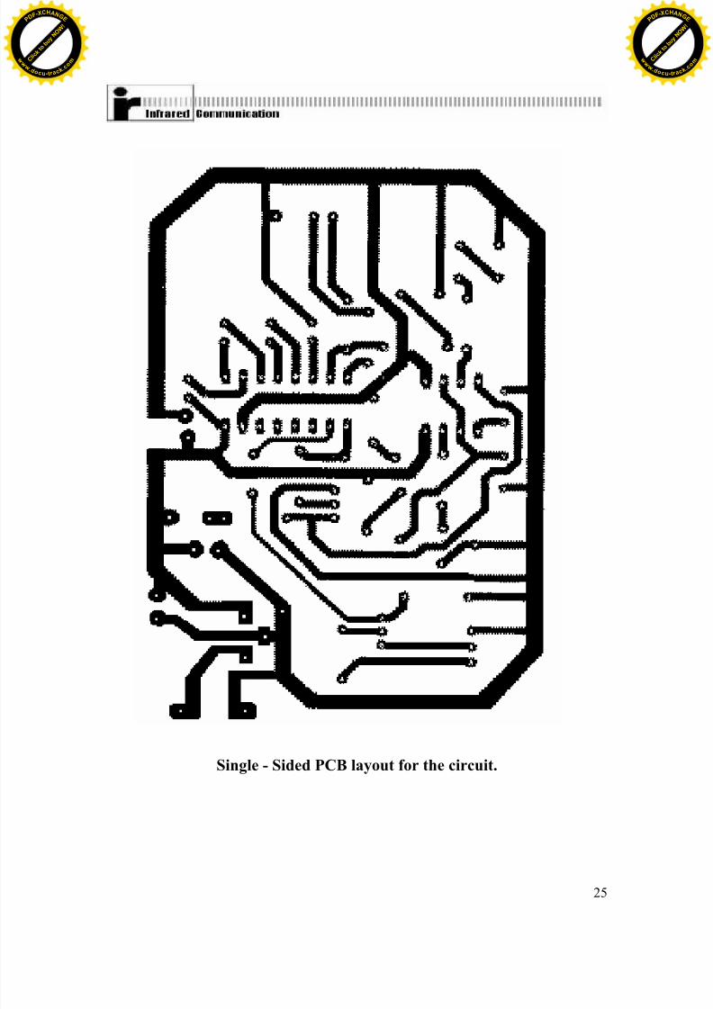
Single - Sided PCB layout for the circuit.
C l i c k
t o b u y N
O W !
D F - XCHAN G E
d o c u- t r a c k
. c o m
C l i c k
t o b
P D F - XC
w w w . d
o c u
7/27/2019 reetu hudda
http://slidepdf.com/reader/full/reetu-hudda 26/26
BIBLIOGRAPHY
K.R BOTKAR, INTEGRATED CIRCUITS, NINTH EDITION.
RAMAKANT A. GAYAKWAD, OP-AMPS AND LINEAQR
INTEGRATED CIRCUITS, THIRD EDITION.
R.P SINGH AND S.D SAPRE, COMMUNICATION SYSTEMS
ANALOG AND DIGITAL, FIRST EDITION.
ELECTRONICS FOR YOU, MAGAZINE, NOV 2000 ISSSUE.
ELECTOR ELECTRONICS, MARCH-APRIL 2000 ISSUE.
COMMUNICATION SYSTEMS BY SIMON HAYKENS, SECOND
EDITION.
PRINCIPLES OF COMMUNICATION SYSTEMS BY HERBERT
TAUB AND DONALD L. SCHILLING, SECOND EDITION.
http://www.angelfire.com/electronic
http://www.electronicsforu.com
http://www.ee.ed.ac.uk/~kap/Hard/555
C l i c k
t o b u y N
O W !
D F - XCHAN G E
d o c u- t r a c k
. c o m
C l i c k
t o b
P D F - XC
w w w . d
o c u