ref : r&d.e53.rp.01192.astr...
TRANSCRIPT

Eur1553
Ref : R&D.E53.RP.01192.ASTR Edition : 01 Rév. : 01 Date : 2009/12/02 Page : 1/60
© EADS ASTRIUM SAS
Project : contract n° 20041/06/NL/CP
Europeanisation of Mil-STD-1553B Data Bus Products
Task 1 – Digital Remote Terminal ASIC
RT53eur IP Core Data Sheet
Name and Function Date Signature
Prepared by Arnaud Wagner 1553B Expert
2009/12/02
Verified by
Marc Souyri ASIC expert
2009/12/02
Authorized by Nicolas BEHOT 1553 product Manager
2009/12/02
Document type N° WBS Key words :

Eur1553
Ref : R&D.E53.RP.01192.ASTR Edition : 01 Rév. : 01 Date : 2009/12/02 Page : 2/60
© EADS ASTRIUM SAS
SUMMARY
This document is written in the frame of ESA R&D AO/1-5052/06/NL/CP Europeanisation of “MIL STD 1553B Data Bus”.
It is part of task 1 related to the development of the RT53eur IP
This document is the data sheet of RT53eur IP that is a MIL STD 1553B Remote Terminal

Eur1553
Ref : R&D.E53.RP.01192.ASTR Edition : 01 Rév. : 01 Date : 2009/12/02 Page : 3/60
© EADS ASTRIUM SAS
DOCUMENT CHANGE LOG
Issue/
Revision Date Modified pages Observations
00/00 2009/09/04 preliminary version
01/00 2009/11/02 First issue
01/01 2009/12/02 42,43 detail Buslevel selection
PAGE ISSUE RECORD Issue of this document comprises the following pages at the issue shown
Page Issue/ Rev.
Page Issue/ Rev.
Page Issue/ Rev.
Page Issue/ Rev.
Page Issue/ Rev.
Page Issue/ Rev.
All 01.00

Eur1553
Ref : R&D.E53.RP.01192.ASTR Edition : 01 Rév. : 01 Date : 2009/12/02 Page : 4/60
© EADS ASTRIUM SAS
TABLE OF CONTENTS
TABLE OF CONTENTS..................................................................................................................4
1. INTRODUCTION ...................................................................................................................6
2. DOCUMENTS, ACRONYMS AND CONVENTIONS..........................................................7
2.1 APPLICABLE DOCUMENTS.........................................................................................................................7 2.2 ACRONYMS ..................................................................................................................................................8 2.3 DEFINITION OF TERMS ..............................................................................................................................9 2.4 CONVENTIONS ....................................................................................................................................10
2.4.1 BIT numbering .........................................................................................................................................10 2.4.2 DATA entity...........................................................................................................................................10 2.4.3 BIT definition ...........................................................................................................................................10 2.4.4 Word numbering in the 1553 frame ..........................................................................................................10
3. DESCRIPTION OF RT53EUR IP IN ITS ENVIRONMENT ............................................ 11
4. GENERAL FUNCTIONAL DESCRIPTION....................................................................... 13
4.1 OPERATING MODES.................................................................................................................................13 4.2 CONFIGURATION AT POWER UP.............................................................................................................15 4.3 CONFIGURATION BY REGISTERS ...........................................................................................................16
4.3.1 Configuration register management.............................................................................................................16 4.3.2 Configuration Register description ..............................................................................................................17
5. 1553B PROTOCOL MANAGEMENT DESCRIPTION....................................................... 19
5.1 COMPLIANCE TO THE STANDARD .........................................................................................................19 5.2 INITIALIZATION........................................................................................................................................19 5.3 COMMAND FORMAT.................................................................................................................................19 5.4 INTERNAL REGISTERS RELATED TO 1553B PROTOCOL ....................................................................19
5.4.1 The 1553 Status word register ..................................................................................................................20 5.4.1.1 1553 Command Word Register......................................................................................................................................21 5.4.1.2 1553 Built-In-Test (BIT) word register.........................................................................................................................21 5.4.1.3 1553B State registers updating........................................................................................................................................22
5.5 MODE COMMANDS MANAGEMENT ....................................................................................................22 5.6 NO RESPONSE TIME-OUT MANAGEMENT............................................................................................23 5.7 REDUNDANCY MANAGEMENT...............................................................................................................24 5.8 TEST SUPPORT & ERROR REPORT .........................................................................................................24
5.8.1 Loop test ...................................................................................................................................................24 5.8.2 Transmission time-out ...............................................................................................................................24 5.8.3 “Data wrap around Test” and “Self test” .................................................................................................24
6. THE APPLICATION INTERFACE DESCRIPTION .........................................................25
6.1 ILLEGALIZATION MECHANISM ..............................................................................................................25 6.2 THE MEMORY MANAGEMENT................................................................................................................28

Eur1553
Ref : R&D.E53.RP.01192.ASTR Edition : 01 Rév. : 01 Date : 2009/12/02 Page : 5/60
© EADS ASTRIUM SAS
6.2.1 EDAC protection.....................................................................................................................................28 6.2.2 Direct addressing .......................................................................................................................................29 6.2.3 Indirect addressing .....................................................................................................................................30 6.2.4 Indirect Stacked mode................................................................................................................................32
6.2.4.1 Memory mapping ..............................................................................................................................................................32 6.2.4.2 Stack mechanism ...............................................................................................................................................................34 6.2.4.3 Circular Buffer mechanism .............................................................................................................................................34
6.2.5 Data Block Descriptor ..............................................................................................................................35 6.2.6 Subaddress busy management ....................................................................................................................35 6.2.7 Processing..................................................................................................................................................35
6.3 RTC MANAGEMENT.................................................................................................................................36 6.4 THE INTERRUPT MANAGEMENT............................................................................................................37
7. INTERFACE DESCRIPTION ..............................................................................................39
7.1 REGISTER MAPPING AND ACCESS..........................................................................................................39 7.2 1553B TRANSCEIVER INTERFACE .........................................................................................................42 7.3 APPLICATION INTERFACE DESCRIPTION.............................................................................................44
7.3.1 WaitStates and CSREADYN mechanism.............................................................................................44 7.3.2 Arbitration mechanism..............................................................................................................................44 7.3.3 Errors management ...................................................................................................................................44
8. SIGNAL CHARACTERISTICS..............................................................................................46
8.1 DESCRIPTION AND STATE AT RESET.....................................................................................................46
9. ELECTRICAL REQUIREMENTS .......................................................................................52
9.1 AC CHARACTERISTICS..............................................................................................................................52 9.1.1 Clock characteristics ..................................................................................................................................52 9.1.2 Typical timings given as an example ..........................................................................................................53
10. IP PORT MAP.....................................................................................................................58
Eur1553
Ref : R&D.E53.RP.01192.ASTR Edition : 01 Rév. : 01 Date : 2009/12/02 Page : 6/60
© EADS ASTRIUM SAS
1. INTRODUCTION
This document is written in the frame of ESA R&D AO/1-5052/06/NL/CP Europeanization of “MIL
STD 1553B Data Bus”. It is part of task 1 related to the development of a Digital RT IP performing a
1553B Remote Terminal. This document is the data sheet of the IP core.
The IP is called RT53eur .
• RT stands for Remote Terminal
• 53 is a reminder for 1553B Data Bus
• EUR reminds that the IP has been developed within the " Europeanisation of Mil-STD-1553B
Data Bus Products". Moreover the IP core includes some of the new features defined within the
ECSS 5013 "MIL STD 1553 B extension" working group.

Eur1553
Ref : R&D.E53.RP.01192.ASTR Edition : 01 Rév. : 01 Date : 2009/12/02 Page : 7/60
© EADS ASTRIUM SAS
2. DOCUMENTS, ACRONYMS AND CONVENTIONS
2.1 APPLICABLE DOCUMENTS
AD-2: ECSS Q60-02: Final Draft ASIC/FPGA Development Standard,
http://www.estec.esa.nl/microelectronics/asic/Final-Draft-ECSS-Q-60-02.pdf
AD-6 MIL-STD-1553B, Notice 1-4, 15 January 1996 “Digital Time Division Command/Response Multiplex Data Bus“.
AD-7 MIL-HDBK-1553A, “Multiplex applications Handbook”, 1 Nov 1988 http://ams.aeroflex.com/ProductFiles/AppNotes/milhbk1553a.pdf
AD-8 SAE AS4112, January 1989 “Production Test Plan For the Digital Time Division Command/Response Multiplex Data Bus Remote Terminals
AD-9: SAE AS4111, Issue 1998-10 “Validation Test Plan For the Digital Time Division Command/Response Multiplex Data Bus Remote Terminals
AD-11 AO/1-5052/06/NL/CP - Europeanisation of MIL-STD-155B Data Bus Products – Statement of Work
AD-12 Plan d’Assurance Qualité ASIC - CDSQ.BA.058.INF – Issue 03 rev.00.
AD-14 ASP54 Transceiver ASIC Specification - Astrium – R&D.E53.NT.00461.V.ASTR issue 1.04

Eur1553
Ref : R&D.E53.RP.01192.ASTR Edition : 01 Rév. : 01 Date : 2009/12/02 Page : 8/60
© EADS ASTRIUM SAS
2.2 ACRONYMS
AD Applicable Document ASIC Application Specific Integrated Circuit ASSP Application Specific Standard Product CDR Critical Design Review CPPA Central Part Procurement Agency CPU Central Processor Unit DDR Detailed Design Review DFF D-Type Flip Flop DRC Design Rule Check DSP Digital Signal Processor EDAC Error Detection And Correction ESA European Space Agency
ESTEC European Space Research and Technology Centre
FDIR Failure Detection Isolation and Recovery
FPGA Field Programmable Gate Array GEO Geosynchronous Equatorial Orbit I/O Input/Output ID Identification
IDR Initial Design Review = Specification Requirement Review
IEEE Institute of Electrical and Electronics Engineers
IP Intellectual Property ITT Invitation To Tender
JTAG Joint Test Action Group (refer to IEEE std 1149.1)
LEO Low Earth Orbit LET Linear Energy Transfer LVS Layout Versus Schematic PCB Printed Circuit Board
PDF Portable Document Format PDR Preliminary Design Review PID Process Identification Document PRT Packet Remote Terminal RD Reference Document RT 1533 Remote Terminal SCC Space Components Co-ordination group SCoC Spacecraft Controller on a Chip
SEE Single Event Effect (or SEP Single Event Phenomena)
SEL Single Event Latch up SEP see SEE SET Single Event Transient SEU Single Event Upset SOC System-On-a-Chip SRAM Static Random Access Memory
SRR Specification Requirement Review = Initial Design Review
SRT Simple Remote Terminal TC TeleCommand TID Total Integrated Dose TM TeleMetry TRP Technological Research Programme
VHDL VHSIC Hardware Description Language, IEEE standard 1076
VLSI Very Large Scale Integration (component)
VTP Validation Test Plan (Standard 1553B Test Plan for Remote Terminal )
WP Work Package WWW World Wide Web

Eur1553
Ref : R&D.E53.RP.01192.ASTR Edition : 01 Rév. : 01 Date : 2009/12/02 Page : 9/60
© EADS ASTRIUM SAS
2.3 DEFINITION OF TERMS
Bus Controller (BC) The Bus Controller’s task is to initiate and control all data transfer on the Mil Std 1553B Data Bus. It is the sole device allowed to transmit Command Words.
Remote terminal (RT) The Remote Terminal is used to interface the subsystems to the Mil Std 1553B Data Bus system and perform data transmissions on the Mil Std 1553B Data Bus as controlled by the Bus Controller.
Bus Monitor The Bus Monitor’s task is to listen to the Mil Std 1553B Data Bus traffic and to extract selected information to be used at a later time.
Mil Std 1553 Data Bus All the hardware including cables, isolation resistors, transformers etc. required to provide a data path between the Bus Controller and all the associated Remote Terminals.
Message A single Message is the transmission of a Command Word, Status and Data Words (if they are specified).
Mode Command Command Word in which the Subaddress Field is set to ‘00000’ or ´11111´and a Mode Code is transferred from the Bus Controller to the Remote Terminal.
Receive Command Message with a data flow from the Bus Controller to the Remote Terminal.
Transmit Command Command Word in which the Subaddress Field is set different to ‘00000’ or ´11111´and the subsequent transfer of Data Word(s) from the Remote Terminal to he Bus Controller is initiated.
Transmit Message Message with a data flow from the Remote Terminal to the Bus Controller.
Vector Word Data Word provided by the Remote Terminal subsequent to the Status Word in answer to a Mode Command Transmit Vector Word.
Bit Order The most significant bit shall be transmitted first with the less significant bits following in descending order of value in the Data Word.
Redundant Bus The redundant data bus implements a particular approach for obtaining multiple data paths to improve message arrival probability.
Bus Switching When an RT is receiving or operating on a message on one bus, and another valid, legal command to the RT occurs on the opposite bus later in time.
Superseeding Command When an RT is processing a command, a second valid command word sent to an RT shall take precedence over the previous command. After the minimum intermessage gap time has been exceeded, the RT shall respond to the second valid command when it is not transmitting on that data bus.

Eur1553
Ref : R&D.E53.RP.01192.ASTR Edition : 01 Rév. : 01 Date : 2009/12/02 Page : 10/60
© EADS ASTRIUM SAS
2.4 CONVENTIONS
2.4.1 BIT numbering
Bit n° 0 refers to LEAST Significant Bit (LSB) Bit n° 15 refers to MOST Significant Bit (MSB) For 1553 interface, as given in RD4, the Bit 15 (MSB) in registers corresponds to the 4th bit of a 1553 word.
2.4.2 DATA entity
“Word” refers to 16 Bits data entity “Byte” refers to 8 Bits data entity
“BITi..BIT0” indicates value binary coded in BITi TO BIT0, BITi being the most significant bit
“0XNIBi..NIB0” indicates value hexadecimally coded in NIBi TO NIB0, NIBi being the most significant nibble
For instance, ‘1111000010101010’ and 0xF0AA indicates the same word value.
2.4.3 BIT definition
A bit in a register is set when its value is 1 reset when its value is 0
2.4.4 Word numbering in the 1553 frame
The first data word transmitted in a 1553B message shall be numbered as DW 1, the second transmitted shall be numbered as DW 2 and so on.

Eur1553
Ref : R&D.E53.RP.01192.ASTR Edition : 01 Rév. : 01 Date : 2009/12/02 Page : 11/60
© EADS ASTRIUM SAS
• A stable oscillator that delivers the IP clock frequency
• Two 1553B Transformers
• Two single 1553B Transceivers, or a dual 1553B Transceiver
The RT53eur IP block diagram is depicted in Erreur ! Source du renvoi introuvable.. It can be functionally divided in 2 parts: the 1553B interface and the Application Interface. The RT53eur IP contains the following functions:
3. DESCRIPTION OF RT53EUR IP IN ITS ENVIRONMENT
The RT53eur IP is a 1553B Remote Terminal. When used in nominal and redundant mode, it is connected to the 1553B bus with the following elements, as depicted in Figure 1:
• An application management function
• A protocol management function
• A redundancy management function
• A nominal and a redundant Manchester encoder
• A nominal and a redundant Manchester decoder
Figure 1 : RT53eur IP functional description

Eur1553
Ref : R&D.E53.RP.01192.ASTR Edition : 01 Rév. : 01 Date : 2009/12/02 Page : 12/60
© EADS ASTRIUM SAS
Figure 2 : RT53eur IP block diagram

Eur1553
Ref : R&D.E53.RP.01192.ASTR Edition : 01 Rév. : 01 Date : 2009/12/02 Page : 13/60
© EADS ASTRIUM SAS
4. GENERAL FUNCTIONAL DESCRIPTION
4.1 OPERATING MODES
The RT53eur IP is able to operate in the following modes: Hardware Reset, Initialization, Operational. The management of the RT53eur IP operating behaves as depicted in the flow chart given in Figure 3 and in Figure 4. Initialization mode is activated when the application sets the APPINIT pin. In this mode, RT53eur IP is frozen concerning 1553B bus operation. It allows the application to initialize RT53eur IP registers and the shared memory.
Figure 3 :RT53eur IP Functional Modes flow chart

Eur1553
Ref : R&D.E53.RP.01192.ASTR Edition : 01 Rév. : 01 Date : 2009/12/02 Page : 14/60
© EADS ASTRIUM SAS
Important Note: APPINIT pin shall be used only to allow the application to program RT53eur IP registers and to initialize the shared memory after a reset. APPINIT shall not be used, to take the control of the application bus since it would make APS53 mute for the 1553 exchanges.
State Action Answer to 1553B bus
Answer to user
RT53eur IP OFF No action No answer No answer
Reset state All reset No answer No answer
Initialisation
Freeze RT53eur IP to allow safe initialization of register and shared memory by application
No answer Nominal
RT53eur IP operational Nominal Nominal Nominal
Figure 4 :RT53eur IP Functional Mode description
A single main clock CLK is provided to the RT53eur IP. The Clock Frequency is selectable in the range:
10MHz to 24 MHz by steps of 2MHz. It must be noticed that this range is limited in 3V mode as detailed in section 9.
The clock frequency depends on the SELCK<2..0> pin :
• SELCK<2..0> =000 : 10 Mhz
• SELCK<2..0> =001 : 12 Mhz • SELCK<2..0> =010 : 14 Mhz
• SELCK<2..0> =011 : 16 Mhz
• SELCK<2..0> =100 : 18 Mhz
• SELCK<2..0> =101 : 20 Mhz
• SELCK<2..0> =110 : 22 Mhz
• SELCK<2..0> =111 : 24 Mhz.
The RESETN signal is used to either asynchronously or synchronously reset the RT53eur IP. Two versions of the core are provided. It allows the user to select which one is suited for its application. A synchronous reset is recommended when the asynchronous reset tree is sensitive to SET as for ATMEL ATC18RHA or STM 65 nm processes.
Eur1553
Ref : R&D.E53.RP.01192.ASTR Edition : 01 Rév. : 01 Date : 2009/12/02 Page : 15/60
© EADS ASTRIUM SAS
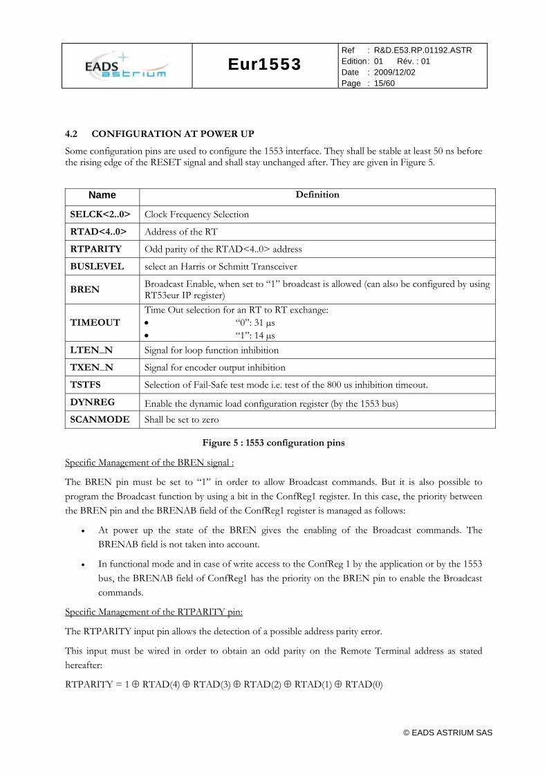
4.2 CONFIGURATION AT POWER UP
Some configuration pins are used to configure the 1553 interface. They shall be stable at least 50 ns before the rising edge of the RESET signal and shall stay unchanged after. They are given in Figure 5.
Name Definition
SELCK<2..0> Clock Frequency Selection
RTAD<4..0> Address of the RT
RTPARITY Odd parity of the RTAD<4..0> address
BUSLEVEL select an Harris or Schmitt Transceiver
BREN Broadcast Enable, when set to “1” broadcast is allowed (can also be configured by using RT53eur IP register)
TIMEOUT Time Out selection for an RT to RT exchange: • “0”: 31 µs • “1”: 14 µs
LTEN_N Signal for loop function inhibition
TXEN_N Signal for encoder output inhibition
TSTFS Selection of Fail-Safe test mode i.e. test of the 800 us inhibition timeout.
DYNREG Enable the dynamic load configuration register (by the 1553 bus) SCANMODE Shall be set to zero
Figure 5 : 1553 configuration pins
Specific Management of the BREN signal :
The BREN pin must be set to “1” in order to allow Broadcast commands. But it is also possible to program the Broadcast function by using a bit in the ConfReg1 register. In this case, the priority between the BREN pin and the BRENAB field of the ConfReg1 register is managed as follows:
• At power up the state of the BREN gives the enabling of the Broadcast commands. The BRENAB field is not taken into account.
• In functional mode and in case of write access to the ConfReg 1 by the application or by the 1553 bus, the BRENAB field of ConfReg1 has the priority on the BREN pin to enable the Broadcast commands.
Specific Management of the RTPARITY pin:
The RTPARITY input pin allows the detection of a possible address parity error.
This input must be wired in order to obtain an odd parity on the Remote Terminal address as stated hereafter:
RTPARITY = 1 ⊕ RTAD(4) ⊕ RTAD(3) ⊕ RTAD(2) ⊕ RTAD(1) ⊕ RTAD(0)

Eur1553
Ref : R&D.E53.RP.01192.ASTR Edition : 01 Rév. : 01 Date : 2009/12/02 Page : 16/60
© EADS ASTRIUM SAS
The RTPARITY input is checked for each valid command received. If the check reflects a parity error, the 1553 interface will not process the command.
4.3 CONFIGURATION BY REGISTERS
4.3.1 Configuration register management
The configuration information are stored in four Configuration registers:
• Register 1 : RT Mode definition
• Register 2 : Real Time Clock definition
• Register 3 : Interrupt Mask definition
• Register 4 : Application Interface definition
The Configuration registers can be read and written through the application data bus as specified in section 7.1. But 3 of the 4 Configuration registers can also be read and written through the 1553 bus if the DYNREG pin is asserted. In this case, the Configuration registers 1, 2 and 3 are read and written through the 1553 bus by using the 0x01 sub-address. A 1553B message can contain up to 32 data words, but RT53eur IP uses the following words to read and write in the configuration registers:
• Register 1 corresponds to word 17 of the 1553 message
• Register 2 corresponds to word 18 of the 1553 message
• Register 3 corresponds to word 19 of the 1553 message
• Register 4 is not accessible through the 1553 bus
In case DYNREG is activated and if a valid receive message is issued at 0x01 subaddress then:
• If the number of words is smaller or equal to 16, no update of configuration register is performed.
• If the number of words is between 17 and 219, 1 to 3 configuration registers are updated.
• If the number of words is greater than 19, the 3 registers are updated.
The dynamic update of the registers is performed at the end of the receipt, during the writing of the Data Block descriptor. In addition, a message used to dynamically update the Configuration registers is processed as an usual message and all the data are provided to the application normally.

Eur1553
Ref : R&D.E53.RP.01192.ASTR Edition : 01 Rév. : 01 Date : 2009/12/02 Page : 17/60
© EADS ASTRIUM SAS
4.3.2 Configuration Register description
Name Function Word number
in 1553 message
Address
mapping
ConfReg1 RT mode definition 17 0x0000 ConfReg2 Real Time Clock definition 18 0x0001 ConfReg3 Interrupt Mask definition 19 0x0002 ConfReg4 Application Interface Configuration definition N.A. 0x0003
Figure 6 : List of the Configuration registers
ad = 0x0000 ConfReg1 RT mode
Bits Name Function Reset Value
15..5 - Not Used 0
4 CURSTACK “1” : Current Stack Pointer B is selected “0” : Current Stack Pointer A is selected
0
3 EDACEN “1” : EDAC is enabled “0” : EDAC is disabled
0
2 INTWRAP “1” : RT53eur IP Internal Data Wrap Around subaddress 30 “0” : Application Data Wrap Around subaddress 30
1
1 ILLENAB “1” : Illegalization mechanism enabled “0” : Illegalization mechanism disabled
0
0 BRENAB “1” : Broadcast mode enabled “0” Broadcast mode disabled
1
Figure 7 : ConfReg1 RT mode definition
ad = 0x0001 ConfReg2 Real Time Clock
Bits Name Function Reset Value
15..0 FRAMEDUR Frame duration 0
Figure 8 : ConfReg2 Real Time Clock definition

Eur1553
Ref : R&D.E53.RP.01192.ASTR Edition : 01 Rév. : 01 Date : 2009/12/02 Page : 18/60
© EADS ASTRIUM SAS
ad = 0x0002 ConfReg3 Interrupt Mask definition
Bits Name Function Reset Value
15..11 SADSEL Selected Message sub address 0
10..8 STSIZE
Descriptor Stack Buffer Size: 000 : Only One descriptor (5 words) 001 : 128 words 010 : 256 words 011 : 512 words 100 : 1024 words 101 : 2048 words 110 : 4096 words 111 : 8192 words
000
7 EDACDERR EDAC Double Error interrupt activation 0 6 MIDCIBUF Middle Boundary of Circular Buffer Interrupt Activation 0 5 RTERROR Remote Terminal protocol error Interrupt Activation 0 4 TIOVER Time Tag Rollover Interrupt Activation 0 3 CIOVER Circular Buffer Rollover Interrupt Activation 0 2 STOVER Descriptor Stack Rollover Interrupt Activation 0 1 RTSEL Selected Message Received Interrupt Activation 0 0 ENDMSG End of Message Interrupt Activation 1
Figure 9 : ConfReg3 Interrupt Mask definition
ad = 0x0003 ConfReg4 Application Interface Configuration
Bits Name Function Reset Value
15..4 Not Used 0 3..0 WAITSTATES Number of Wait States during external access 0000
Figure 10 : ConfReg4 Application Interface Configuration definition

Eur1553
Ref : R&D.E53.RP.01192.ASTR Edition : 01 Rév. : 01 Date : 2009/12/02 Page : 19/60
© EADS ASTRIUM SAS
5. 1553B PROTOCOL MANAGEMENT DESCRIPTION
5.1 COMPLIANCE TO THE STANDARD
The 1553B protocol is managed in RT53eur IP in a function that can be called 1553 Interface by opposition to the Application Interface. The 1553 interface is fully compliant with [AD6].
5.2 INITIALIZATION
During “Initialization state” the RT53eur IP has the following behaviour:
• it initializes its registers to their power-up value,
• it does not respond to any request from the 1553B bus,
During the application initialization, APPINIT is asserted high by the application. When APPINIT is activated. the RT53eur IP has the following behaviour:
• it does not respond to any request from the 1553B bus and shall not process the incoming commands.
• the internal registers can be read or write by the application.
5.3 COMMAND FORMAT
RT53eur IP is compliant with all 1553 commands described in Figure 11
Figure 11 : Commands format
5.4 INTERNAL REGISTERS RELATED TO 1553B PROTOCOL

Eur1553
Ref : R&D.E53.RP.01192.ASTR Edition : 01 Rév. : 01 Date : 2009/12/02 Page : 20/60
© EADS ASTRIUM SAS
In operational phase, the 1553 interface of RT53eur IP uses three registers to store state information related to the 1553B protocol. These registers are updated during the transactions on the bus. Their data are maintained between two commands. These registers called “1553B state” registers are:
• the RT status word,
• the BIT (Built-In Test) word
• the Last Command Word.
5.4.1 The 1553 Status word register
This Status register memorizes the current Status word. Its content is depicted in Figure 12. At the reception of the Transmit status Mode command, and each time the 1553 interface answers to a command, the status register is returned onto the bus.
The update conditions of the current status are described in Figure 15.
Bits Name Function Reset Value
15-11 RTAD<4..0> Remote Terminal Address, copy of the hardwired address input pins of the RT53eur IP RTAD<4..0>
10 ME Message Error, set to “1” an error has occurred 0 9 RES Available for application 0 8 SREQ RT requesting service, set to “1” when a service is requested 0 7-5 RES Available for application 0
4 BRX Broadcast command received, set to “1” when the command received is in broadcast mode 0
3 BUSY Address channel not available or treatment still in progress 0
2 SSF Sub System Flag, set to “1” when a sub system fault has occurred 0
1 RES Available for application 0 0 TF Terminal Flag, set to “1” when RT fault has occurred 0
Figure 12 : Status Register Description
An RT fault covers the following cases: Loop error, Time Out during emission and Time Out during application access.
During Transmit BIT word command, the TF bit is forced to “0”. When TF bit is high, the B10..B1 bits are irrelevant.
The RES bits are unused, i.e. its value must be “0”.
The SREQ bit memorizes the value of the SREQ pin at the time the Status Word is updated.
The SSF bit memorizes the value of the SSF pin at the time the Status Word is updated.

Eur1553
Ref : R&D.E53.RP.01192.ASTR Edition : 01 Rév. : 01 Date : 2009/12/02 Page : 21/60
© EADS ASTRIUM SAS
5.4.1.1 1553 Command Word Register
The 1553 Command Word Register contains the last valid Command word addressing the RT53eur IP. The Last Command word content is depicted in Figure 13. The update conditions of the Last command word are described in Figure 15.
Bits Name Function Reset Value
15-11 RTAD<4..0> Remote Terminal Address, copy of the hardwired address input pins of the 1553 interface
RTAD<4..0>
10 T/R Transfer type, “1” stands for transmit, “0” receive 0
9-5 SA<4..0> Sub Address, “00000” or “11111” indicates a mode code for the next field; anything else indicates a data word count for the next field
0
4-0 WC<4..0> Data word count or Mode code 0
Figure 13 : Last command register
5.4.1.2 1553 Built-In-Test (BIT) word register
The BIT Word Register contains the information related to the 1553 interface error status. The BIT Word Register content is depicted in Figure 14. The update conditions of the BIT word are described in Figure 15.
Bits Name Function Reset Value
15-14 “0” Not used in 1553 interface 0 13 TIMOUT1 800µs Time out activation on 1553 bus redundant 0 12 TIMOUT0 800µs Time out activation on 1553 bus nominal 0 11 INHTF Terminal Flag bit inhibited when set to “1” 0 10-8 “0” Not used in 1553 interface 0
7 ERRAPP Application error, set to “1” when timeout activation on application access 0
6 HIDW Number of words received higher than expected 0 5 LODW Number of words received lower than expected 0
4 UND Undefined Mode command, Self-Test or Dynamic Bus Conf Acceptance Mode Code reception 0
3 ILTR Illegal T/R bit in a Mode command 0 2 LP Loop Test Error when set to “1” 0 1 BUSY User interface busy when set to “1” 0
0 TIMOUT 800µs Time out activation on the current active 1553 bus 0
Figure 14 : Built-In Test (BIT) register

Eur1553
Ref : R&D.E53.RP.01192.ASTR Edition : 01 Rév. : 01 Date : 2009/12/02 Page : 22/60
© EADS ASTRIUM SAS
5.4.1.3 1553B State registers updating
The 1553B state registers are updated following the requirements of Figure 15.
Handled command Last Command Status BIT
Transmit last command Not updated Not updated Not updated
Transmit status word Updated Not updated Not updated
Transmit BIT word Updated Updated Not updated
Other valid command words, addressing the 1553 interface Updated Updated Updated
Other commands (invalid, or not addressing the 1553 interface)
Not updated Not updated Not updated
Figure 15 : 1553 interface state registers evolution
5.5 MODE COMMANDS MANAGEMENT
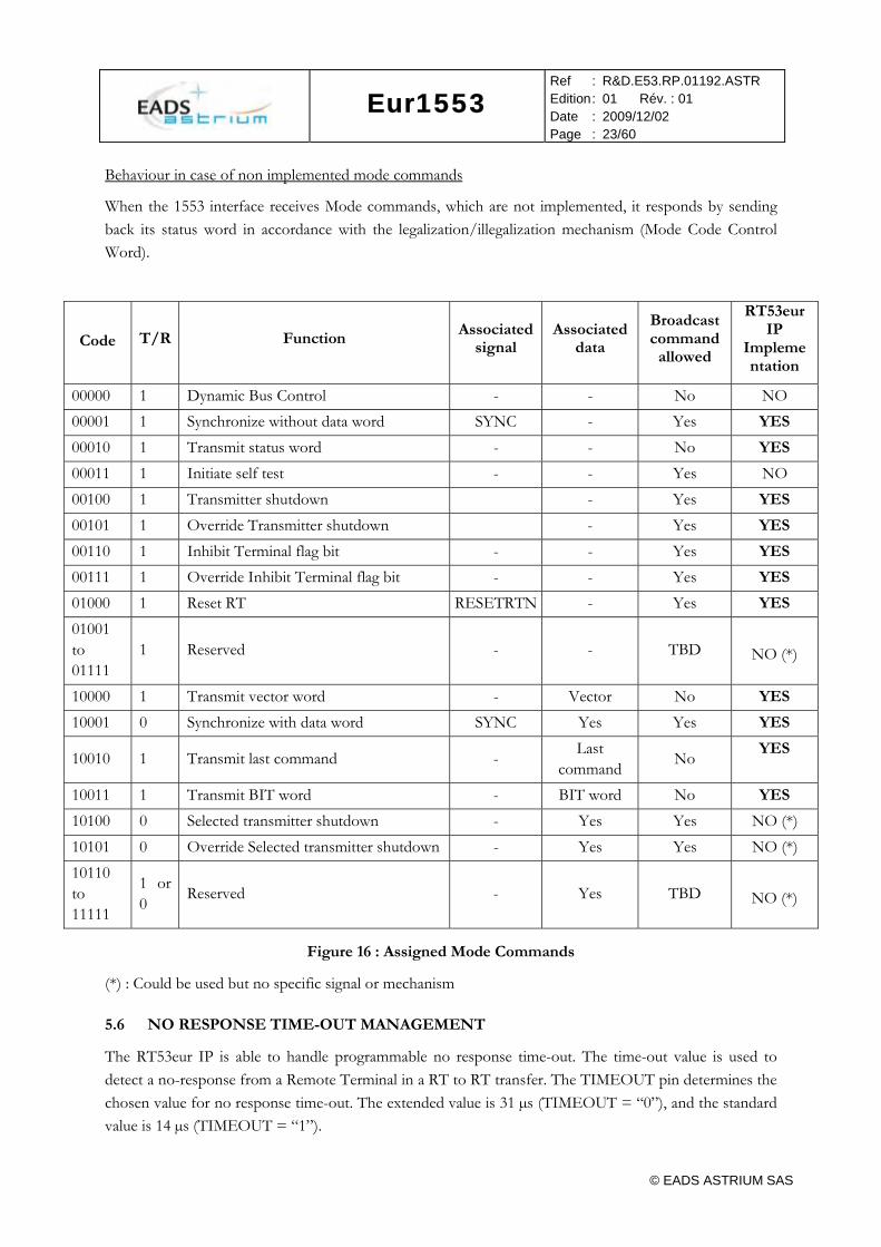
The mode commands implemented in RT53eur IP are described in Figure 16.
Synchronize with or without data word :
The SYNCN signal is generated about 30.5 µs after the mid-parity bit of the command word. The data, if used, is transmitted to the application.
Transmit status word, Transmit last Command:
These two commands are transparent to the application. In accordance to the standard it is not possible to illegalise them.
Reset Remote Terminal Command :
The RT53eur IP activates the RESETRTN signal when a legal Reset RT Command is received. The activation occurs:
• less than 2 us after the end of status emission in case of a non broadcast command.
• just after the command processing (i.e. the writing of the data block descriptor) in case of a broadcast command received.
Transmitter shutdown:
RT53eur IP inhibits the transmitter related to the other bus.
Override transmitter shutdown:
RT53eur IP resets the inhibition of the transmitter related to the other bus.
Eur1553
Ref : R&D.E53.RP.01192.ASTR Edition : 01 Rév. : 01 Date : 2009/12/02 Page : 23/60
© EADS ASTRIUM SAS
Behaviour in case of non implemented mode commands
When the 1553 interface receives Mode commands, which are not implemented, it responds by sending back its status word in accordance with the legalization/illegalization mechanism (Mode Code Control Word).
Code T/R Function Associated
signal Associated
data
Broadcast command
allowed
RT53eur IP
Implementation
00000 1 Dynamic Bus Control - - No NO 00001 1 Synchronize without data word SYNC - Yes YES
00010 1 Transmit status word - - No YES
00011 1 Initiate self test - - Yes NO 00100 1 Transmitter shutdown - Yes YES
00101 1 Override Transmitter shutdown - Yes YES
00110 1 Inhibit Terminal flag bit - - Yes YES 00111 1 Override Inhibit Terminal flag bit - - Yes YES 01000 1 Reset RT RESETRTN - Yes YES
01001 to 01111
1 Reserved - - TBD
NO (*)
10000 1 Transmit vector word - Vector No YES 10001 0 Synchronize with data word SYNC Yes Yes YES
10010 1 Transmit last command - Last command No YES
10011 1 Transmit BIT word - BIT word No YES
10100 0 Selected transmitter shutdown - Yes Yes NO (*) 10101 0 Override Selected transmitter shutdown - Yes Yes NO (*) 10110 to 11111
1 or 0 Reserved - Yes TBD
NO (*)
Figure 16 : Assigned Mode Commands
(*) : Could be used but no specific signal or mechanism
5.6 NO RESPONSE TIME-OUT MANAGEMENT
The RT53eur IP is able to handle programmable no response time-out. The time-out value is used to detect a no-response from a Remote Terminal in a RT to RT transfer. The TIMEOUT pin determines the chosen value for no response time-out. The extended value is 31 µs (TIMEOUT = “0”), and the standard value is 14 µs (TIMEOUT = “1”).

Eur1553
Ref : R&D.E53.RP.01192.ASTR Edition : 01 Rév. : 01 Date : 2009/12/02 Page : 24/60
© EADS ASTRIUM SAS
5.7 REDUNDANCY MANAGEMENT
The 1553 interface is able to detect any incoming command on either the nominal or the redundant bus and to respond on the bus it has been activated by. The content of the internal registers (Status word register, Last Command register and BIT register) always corresponds to the last transfer performed on either nominal or redundant bus.
If a transfer is interrupted on a 1553B bus by a valid command incoming on the other bus and addressing the RT, the 1553 interface stops the processing of the previous command and starts the processing of the new command.
The 1553 interface responds with a BUSY bit set to “1” in its status if the command arrives on the alternate bus during the end of the processing of a reception command on the other bus to avoid a corruption of the data.
5.8 TEST SUPPORT & ERROR REPORT
5.8.1 Loop test
When RT53eur IP emits on the 1553B bus, its reception function monitors simultaneously the real bus state. It allows checking the correct connections and behaviours of the 1553B Transceiver and of the Transformer. Such feature is called the “loop test”.
In case of difference between the emitted message and the received one, the 1553 interface inhibits the current emission within a delay of 3 µs, sets the TF bit in the internal status register and indicates the error nature in the BIT word.
This function is enabled only when LTEN_N input pin is at low level.
5.8.2 Transmission time-out
The 1553 interface limits all the emissions of more than 800 µs by using an internal timeout, as required in the 1553B norm. In this case emission must be inhibited. This error induces an update of the BIT word, and the setting of the TF bit of the status word. The transmission inhibition is cancelled at the reception of the next valid command addressing the 1553 interface.
5.8.3 “Data wrap around Test” and “Self test”
The 1553 interface does not implement any “Self Test”.
But a Data Wrap Around Test is implemented using address 30. The data received at this sub address are transmitted when a transmit command at this sub address is received. The transmit command follows the receive command in case of internal wrap around. RT53eur IP manages two kinds of data wrap around test according to the INTWRAP field of ConfReg1:
• An autonomous test: in that case RT53eur IP stores the received data in its internal buffer.
• A normal test: in that case the application must store the received data.
The number of words accepted by the Data wrap around test ranges from 1 to 32.

Eur1553
Ref : R&D.E53.RP.01192.ASTR Edition : 01 Rév. : 01 Date : 2009/12/02 Page : 25/60
© EADS ASTRIUM SAS
6. THE APPLICATION INTERFACE DESCRIPTION
6.1 ILLEGALIZATION MECHANISM
The RT53eur IP can manage an illegalization table stored in memory. The purpose of the illegalization table is to validate an incoming message from its subaddress and from its type. The illegalization mechanism can be activated /deactivated according to the ILLEGAL field of the ConfReg1 configuration register. If the illegalization mechanism is not activated, each incoming message is considered as valid from the illegalization mechanism point of view. But it must be noticed that the illegalization table is always read since it contains the memory mode, busy bit and the circular buffer size (if any) of the incoming message.
The illegalization table has to be built in memory at power up by the application. Such table can be permanently located in a PROM, or be loaded in the memory, or be located in an FPGA connected to RT53eur IP. The illegalization Table is shared in 7 areas which mapping is depending only on the received Command word as depicted in Figure 17 :
• Mode Command in Receipt
• Mode Command in Receipt and Broadcast
• Receive Command
• Receive Command in Broadcast
• Mode Command in Transmit
• Mode Command in Transmit and in Broadcast
• Transmit Command
Within each area, illegalization words are addressed by the subaddress or the mode code value of the message. Each subaddress or mode code must have a subaddress characterization word in the illegalization table. RT53eur IP accesses to the illegalization table at the start of each transfer in order to manage the STATUS word and the data to receive or to transmit
The following mode codes do not have associated characterization word :
• Transmit Status Word
• Transmit last Command
RT53eur IP consider these mode codes as always legal, and they do not generate any traffic on the application.

Eur1553
Ref : R&D.E53.RP.01192.ASTR Edition : 01 Rév. : 01 Date : 2009/12/02 Page : 26/60
© EADS ASTRIUM SAS
Subadress 1 Receive0x0241
Subadress 30 Receive0x025E
Subadress 1 Transmit0x02C1
Subadress 30 Transmit0x02DE
Subadress 1 Receive Broadcast0x0261
Subadress 30 Receive Broadcast0x027E
Mode Code 0 Receive0x0200
Mode Code 31 Receive0x021F
Mode Code 0 Transmit0x0280
Mode Code 31 Transmit0x029F
Mode Code 0 Receive Broadcast0x0220
Mode Code 31 Receive Broadcast0x023F
Mode Code 0 Transmit Broadcast0x02A0
Mode Code 31 Transmit Broadcast0x02BF
Figure 17 : Illegalization Table Addresses
A characterization word for each subaddress contains the information given in Figure 18 and for mode code the information given in Figure 19 .

Eur1553
Ref : R&D.E53.RP.01192.ASTR Edition : 01 Rév. : 01 Date : 2009/12/02 Page : 27/60
© EADS ASTRIUM SAS
Bits Name Function
15..13 Not Used
12..10 BUFSIZE
Circular Buffer Size: 000 : 64 words 001 : 128 words 010 : 256 words 011 : 512 words 100 : 1024 words 101 : 2048 words 110 : 4096 words 111 : 8192 words
9 BUSY
Data Block in memory availability : 0 : Data Block available 1 : Data Block are not ready to be Read or Writen over by RT53eur IP.
8 CHECK RT53eur IP shall check data word count : 0 : No 1 : Yes
7..6 MODE
Memory Mode 00 : Direct Addressing 10 : Indirect Addressing 01 : Indirect Stacked Addressing
5..1 DWC Data Word Count 0 : 32 words 1..31 : same
0 ILLSA legality (ME bit in STATUS WORD) 0 : Legal 1 :Illegal
Figure 18 : Subaddress Characterization Word
Bits Name Function
15..1 Not Used
0 ILLMC legality (ME bit in STATUS WORD) 0 : Legal 1 :Illegal
Figure 19 : Mode Code Characterization Word

Eur1553
Ref : R&D.E53.RP.01192.ASTR Edition : 01 Rév. : 01 Date : 2009/12/02 Page : 28/60
© EADS ASTRIUM SAS
6.2 THE MEMORY MANAGEMENT
The memory management is configurable in one of these 3 modes: • the Direct addressing • the Indirect addressing • the Indirect Stacked addressing
The Direct Addressing mode and the Indirect Addressing mode are similar. In the Direct Addressing mode each message is stored at a unique address depending only on the content of the received command word. The Indirect Addressing mode provides an indirect addressing mechanism allowing to store the message more freely. The Indirect Stacked mode manages circular buffers to store the data and the data block descriptors.
The access to the characterization table is made by using a specific chip selection signal called CHARSN.
All the memory exchanges are protected by an EDAC.
6.2.1 EDAC protection
The RT53eur IP embeds an EDAC able to detect and correct one error in memory. The EDAC is based on the Hamming code depicted in Figure 20. When enabled the RT53eur IP manages 6 extra bits in the Data bus named DATAC0 to DATAC5. This EDAC shall be enabled only when EDACEN field of the Confreg1 Configuration Register is active. In case of single error, the SERRN signal is activated. In case of double error, the DERRN signal is activated. If the double error occurs during a message processing, the RT53eur IP sets the TF bit of the Status Word returned, and raises an interrupt. RT53eur IP does not correct double errors. It is assumed that the application implements a scrubbing mechanism that is in charge of managing double errors.
CHECK BITS
0 1 2 3 4 5 6 7 8 9 10 11 12 13 14 15
DATAC0 XNOR X X X X X X X X
DATAC1 XNOR X X X X X X X X
DATAC2 XOR X X X X X X X X
DATAC3 XOR X X X X X X X X
DATAC4 XOR X X X X X X X X
DATAC5 XOR X X X X X X X X
Figure 20 : EDAC definition

Eur1553
Ref : R&D.E53.RP.01192.ASTR Edition : 01 Rév. : 01 Date : 2009/12/02 Page : 29/60
© EADS ASTRIUM SAS
6.2.2 Direct addressing
The memory mapping of the Direct Addressing mode is described in Figure 21 and in Figure 22. The address is only command dependant. The memory is shared in the following areas:
• The Last data Block Descriptor area is composed of 5 words that store the Command Word, the Status Word, the Time Tag Word, The Frame Tag Word and the Data Block Pointer. This area is updated at the end of each valid exchange. In this mode only the last descriptor is kept in memory. The Data Block Pointer is the address of the data words in memory.
• The Illegalization table as described in section 6.1.
• The data block area in receive mode
• The data block area in transmit mode
• The data block area in broadcast mode
The size of each reserved data block area is 32 times 32 words. The data related to a message are stored consecutively in memory.
In Direct Addressing, the associated data of mode commands are stored in the “Data Block reception area” corresponding to subaddress 0. The 5 LSB bits of the address are the mode code identifier.
In Direct Addressing, the associated data of a Transmit command at subaddress 30, corresponding to wrap-around , is stored in the Receive area of this subaddress.
0000-0004 Last data Block Descriptor
0200-027E Illegalization table reception
0280-02DE Illegalization table transmission
0800-0BFF Data Block area in reception (direct)
0C00-0FFF Data Block area in transmission (direct)
1800-1BFF Data Block area in broadcast (direct)
others Not Used
Figure 21 : Direct Addressing Memory Map
Eur1553
Ref : R&D.E53.RP.01192.ASTR Edition : 01 Rév. : 01 Date : 2009/12/02 Page : 30/60
© EADS ASTRIUM SAS
Figure 22 : Direct addressing
6.2.3 Indirect addressing
In Indirect Addressing mode, the data received or transmitted through a subaddress that is not a mode code command are exchanged with memory using an indirect addressing mechanism. A look-up table stores the indirect address of the first word of each subaddress that does not correspond to a mode code command. The memory mapping is depicted in Figure 23 and in Figure 24.
The memory is shared in the following areas:
• The Last data Block Descriptor area is composed of 5 words that store the Command Word, the Status Word, the Time Tag Word, The Frame Tag Word and the Data Block Pointer. This area is updated at the end of each valid exchange. In this mode only the last descriptor is kept in memory. The Data Block Pointer is the address of the data words in memory.
• The Look Up Table that contains 96 pointers to data blocks corresponding to 32 indirect addresses in receive mode, 32 indirect addresses in transmit mode, and 32 indirect addresses in broadcast mode.
• The Illegalization table as described in section 6.1.
• A mode code command area in reception containing 32 words
• A mode code command area in transmit containing 32 words
• A mode code command area in broadcast containing 32 words

Eur1553
Ref : R&D.E53.RP.01192.ASTR Edition : 01 Rév. : 01 Date : 2009/12/02 Page : 31/60
© EADS ASTRIUM SAS
• The rest of the memory can be used to store data blocks by using the indirection mechanism. The organization of this area is left free to the user.
0000-0004 Last data Block Descriptor
0140-019F Look Up Table
0200-027E Illegalization table reception
0280-02DE Illegalization table transmission
02DF-07FF Free for Data Blocks
0800-081F Mode code command reception
0820-0BFF Free for Data Blocks
0C00-0C1F Mode code command emission
0C20-17FF Free for Data Blocks
1800-181F Mode code command broadcast
1820-FFFF Free for Data Blocks
Figure 23 : Indirect addressing Memory Map
Data Subaddress 1 Receive
…...
DATA 31 (last)
DATA 0 (first)
Data Subaddress 30 Broadcast
…...
DATA 31 (last)
DATA 0 (first)
COMMAND WORD
…...
LOOK-UP TABLE
…...
Last Block Descriptor
STATUS WORD
TIME TAG WORD
DATA BLOCK POINTER
RECEIVED COMMAND WORD0000
0001
0002
0003
0004
SLOT TIME WORD
D.B. Pointer Subaddress 1 Broadcast
D.B. Pointer Subaddress 1 Transmit
D.B. Pointer Subaddress 1 Receive
D.B. Pointer Subaddress 30 Broadcast
D.B. Pointer Subaddress 30 Transmit
D.B. Pointer Subaddress 30 Receive
Figure 24 : Indirect addressing

Eur1553
Ref : R&D.E53.RP.01192.ASTR Edition : 01 Rév. : 01 Date : 2009/12/02 Page : 32/60
© EADS ASTRIUM SAS
6.2.4 Indirect Stacked mode
6.2.4.1 Memory mapping
The memory mapping of the Indirect Stacked mode is described in Figure 25.
In Indirect Stacked mode, the data received or transmitted through a subaddress that does not correspond to a mode code command, are exchanged with memory using an indirect addressing mechanism. A look-up table stores the indirect addressing for the first word of each subaddress that is not a mode code command, as depicted in Figure 26.
In Indirect Stacked mode, RT53eur IP stores all the data Block Descriptors in a stack.
The memory is shared in the following areas:
• The Stack pointer A and B words contain the addresses of the Data Block Descriptor A and B.
• The Last data Block Descriptor area is composed of 5 words that store the Command Word, the Status Word, the Time Tag Word, The Frame Tag Word and the Data Block Pointer. This area is updated at the end of each valid exchange. The Data Block Pointer is the address of the data words in memory.
• The Look Up Table that contains 90 pointers to data blocks corresponding to 30 indirect addresses in receive mode, 30 indirect addresses in transmit mode, and 30 indirect addresses in broadcast mode.
• The Illegalization table as described in section 6.1.
• A mode code command area in reception containing 32 words
• A mode code command area in transmit containing 32 words
• A mode code command area in broadcast containing 32 words
• The rest of the memory can be used to store data blocks. The organization of this area is left free to the user.

Eur1553
Ref : R&D.E53.RP.01192.ASTR Edition : 01 Rév. : 01 Date : 2009/12/02 Page : 33/60
© EADS ASTRIUM SAS
0100 Stack Pointer A
0104 Stack Pointer B
0140-019F Look Up Table
0200-027E Illegalization table reception
0280-02DE Illegalization table transmission
02DF-07FF Free for Data Blocks
0800-081F Mode code command reception
0820-0BFF Free for Data Blocks
0C00-0C1F Mode code command emission
0C20-17FF Free for Data Blocks
1800-181F Mode code command broadcast
1820-FFFF Free for Data Blocks
Figure 25 : Indirect Stacked Addressing Memory Map
Figure 26 : Indirect Stacked addressing and stack management

Eur1553
Ref : R&D.E53.RP.01192.ASTR Edition : 01 Rév. : 01 Date : 2009/12/02 Page : 34/60
© EADS ASTRIUM SAS
6.2.4.2 Stack mechanism
The stack mechanism uses 2 pointers which means that 2 stacks A and B are present in memory. The 2 stack pointers are stored at a fixed address in memory. RT53eur IP uses only one stack ( i.e. one stack pointer) at a time for a given exchange. A flag in the Application Interface Configuration register indicates the stack pointer used to write the next descriptor.
The start address of the stack is defined by the user by initializing the stack pointer. The size of the stack is defined in the Confreg3 configuration register. The start address of the stack must have as many LSB set to zeros as the stack size, i.e. if stack size is 64 words 6 LSB are zeros, if stack size is 128 words 7 LSB bits are zeros, and so on… It allows RT53eur IP to determine the start and end addresses of the stack when knowing the stack pointer and the stack size.
After the processing of a 1553 exchange, the RT53eur IP writes the block descriptor at a location starting at an address equal to the current stack pointer. After writing the descriptor block, RT53eur IP checks if there is enough space remaining in the current stack for the next descriptor block. Enough space means 5 words free, if 4 words or less are available the stack is considered as full.
When the stack is full, the other stack will be used for the next message. The CURSTACK field of the ConfReg4 register is toggled by RT53eur IP. RT53eur IP raises an internal interrupt that is transmitted to the INT pin if the interrupt is not masked.
6.2.4.3 Circular Buffer mechanism
A circular buffer mechanism is used to store the data blocks in Indirect Stacked addressing mode. The sizes of the circular buffers are defined by the user in the illegalization table.
The start addresses of the circular buffers are defined by the user in the Look Up table. The start address of the circular buffers shall have a defined number of LSB bits forced to zero depending on the buffer size. For example, if the buffer size is set to 64 words, the 6 LSB shall be forced to 0. If it is 128 words, 7 LSB shall be forced, and so on. It allows RT53eur IP to determine the start and end addresses of a circular buffer when knowing the current address in the buffer and its size.
RT53eur IP raises an internal interrupt each time the current size of the buffer reach 50% and 100%, that is transmitted to the INT pin if the interrupt is not masked.

Eur1553
Ref : R&D.E53.RP.01192.ASTR Edition : 01 Rév. : 01 Date : 2009/12/02 Page : 35/60
© EADS ASTRIUM SAS
6.2.5 Data Block Descriptor
The Data Block Descriptor stores 5 words related to the last exchange:
• The Command Word
• The 1553 Status Word
• The Time Tag value sampled when the Command word has been received and decoded
• The Frame Tag value sampled when the Command word has been received and decoded
• The Data block pointer that is the start address of the data block related to the exchange. If no data block is associated to the command (in case of Mode Code command without data), this pointer is set to 0x0000.
6.2.6 Subaddress busy management
Each Subaddress uses a busy mechanism to indicate the availability of a data block. The busy mechanism is managed by application via the characterization word. The busy bit of the STATUS is set if the busy bit of the characterization word is set. In this case no data word are transmitted or written in memory.
6.2.7 Processing
When a valid and legal message is received by RT53eur IP, it performs the following accesses in memory:
• Read illegalization word at an address depending only on the information contained in the Command Word.
• Read the Look Up Table at an address depending only on the information contained in the command word. The start address of the data block is read, it is called the data block pointer. (only in indirect and stacked mode)
• Read or Write the data words in the data block.
• Read the Stack Pointer. (only in stacked mode)
• Write the 5 words of the Descriptor Block in the stack.
• Update the Data Block pointer in the Look Up Table. (only in indirect and stacked mode)
• Update the Stack Pointer. (only in stacked mode)

Eur1553
Ref : R&D.E53.RP.01192.ASTR Edition : 01 Rév. : 01 Date : 2009/12/02 Page : 36/60
© EADS ASTRIUM SAS
6.3 RTC MANAGEMENT
The RT53eur IP includes a Real Time Clock Management based on 3 parameters:
• The “time into a frame ” or TimeTag which is a 16 bit counter.
• The “frame number” or FrameTag which is a 16 bit register
• The “Frame Duration” which is a 16 bit register
The TimeTag counter is reset at power up. The TimeTag counter is counting when the Frame Duration is different from zero. Its increment represents 16 us whatever the SELCK clock selection is. When the Frame Duration is equal to zero the TimeTag is stopped and reset.
When the TimeTag counter reaches the Frame Duration, it is reset and an interrupt can be generated according to the TIOVER bit of the Confreg3 Configuration register.
Upon receipt of a Synchronize without or with data word command, the TimeTag counter is reset.
Upon receipt of a Synchronize with data word command, the FrameTag is loaded with the value of the received data word.
The duration between the mid-parity bit of the SYNC command word and the load or reset time is about 30.5 us (+/- 500 ns).

Eur1553
Ref : R&D.E53.RP.01192.ASTR Edition : 01 Rév. : 01 Date : 2009/12/02 Page : 37/60
© EADS ASTRIUM SAS
6.4 THE INTERRUPT MANAGEMENT
RT53eur IP manages the following cause of interrupts:
Nbr Name Function Maskable IT signal
9 APPERR Application Interface Error Interrupt No INT, DERRN8 EDACDERR EDAC Double Error Interrupt Yes INT, DERRN
7 MIDCIBUF Circular Buffer Size reach 50% Interrupt Yes INT
6 RTERROR Remote Terminal protocol error Interrupt Yes INT
5 TIOVER Time Tag Rollover Interrupt Yes INT
4 CIOVER Circular Buffer Rollover Interrupt Yes INT
3 STOVER Descriptor Stack Rollover Interrupt Yes INT
2 RTSEL Selected Message Received Interrupt Yes INT
1 ENDMSG End of Message Interrupt Yes INT
Figure 27 : Interrupt definition
RT53eur IP is able to mask the interrupt numbered 1 to 8 by using the ConfReg3 register fields. Interrupt 8 is activated only if EDAC is enabled. It can be masked also. Interrupt 9 cannot be masked, since it is caused by an application interface error as timeout or bus grant terminated too early by the application.
When an interrupt has been raised, the Interrupt Vector Register is updated accordingly to memorize the interrupt cause as defined above.
All the interrupts except the TimeTag Rollover (n°4) interrupt are reset at the reception of a new valid command word. All the interrupts are reset after a read access to the Interrupt Vector register by the application.
In case of Interrupt that is not a Time Tag Rollover or a Remote Terminal Error, the INT signal is raised at the same time as the TROKN signal at the end of the exchange. In case of Interrupt that is a Time Tag Rollover or a Remote Terminal Error, the INT raises at the time the Interrupt occurs. The INT signal lasts generally one clock cycle. It lasts 2 clock cycles in case a Time Tag Rollover arrives just before or after another interrupt.

Eur1553
Ref : R&D.E53.RP.01192.ASTR Edition : 01 Rév. : 01 Date : 2009/12/02 Page : 38/60
© EADS ASTRIUM SAS
The TROKN signal is activated when the exchange is successfully completed from a 1553 point of view. It indicates that the message has been correctly sent to the Bus Controller in case of Transmit, or that the message has been correctly received in the internal buffer of the IP. The TROKN signal is activated during one cycle after all memory updates related to the exchange.
The following mode commands do not generate a TROKN or INT interrupt:
• Transmit Status Word
• Transmit Last Command
• Transmit BIT word
Nevertheless an application interface error or an EDAC double error can occur after, for example during the read and write performed when the descriptor block is written.
In case of EDAC Double Error or application interface error, the DERRN signal is activated immediately. It is maintained until the end of the current message processing. The user is thus able to check it when TROKN is activated to determine the validity of the descriptor block (see also 7.3)

Eur1553
Ref : R&D.E53.RP.01192.ASTR Edition : 01 Rév. : 01 Date : 2009/12/02 Page : 39/60
© EADS ASTRIUM SAS
7. INTERFACE DESCRIPTION
7.1 REGISTER MAPPING AND ACCESS
The internal register listed in Figure 28 can be accessed in read and/or write by the application. The access to RT53eur IP internal registers is made by requesting the bus access as specified in section 7.3, and activating the CSREGN and RWREG control signals.
AD Name Definition R/
W
Reset
Value
0x0000 ConfReg1 RT Mode Definition Register r/w 0005 0x0001 ConfReg2 RTC Definition Register r/w 0000 0x0002 ConfReg3 Interrupt Mask Register r/w 0001 0x0003 ConfReg4 Application Interface Configuration Register r/w 0000 0x0004 InterruptVec Interrupts Vector Register r/* 0000 0x0005 TimeTag RTC Time Counter r/w 0000 0x0006 FrameTag RTC Frame Register r/w 0000
Figure 28 : Internal Register Mapping
Note * : the Interrupt Vector Register is reset in case of read
The RT53eur IP registers are summarized hereafter.
ad = 0x0000 ConfReg1 RT mode
Bits Name Function Reset Value
15..5 - Not Used 0
4 CURSTACK “1” : Current Stack Pointer B is selected “0” : Current Stack Pointer A is selected
0
3 EDACEN “1” : EDAC is enabled “0” : EDAC is disabled
0
2 INTWRAP “1” : RT53eur IP Internal Data Wrap Around subaddress 30 “0” : Application Data Wrap Around subaddress 30
1
1 ILLENAB “1” : Illegalization mechanism enabled “0” : Illegalization mechanism disabled
0
0 BRENAB “1” : Broadcast mode enabled “0” Broadcast mode disabled
1

Eur1553
Ref : R&D.E53.RP.01192.ASTR Edition : 01 Rév. : 01 Date : 2009/12/02 Page : 40/60
© EADS ASTRIUM SAS
ad = 0x0001 ConfReg2 Real Time Clock
Bits Name Function Reset Value
15..0 FRAMEDUR Frame duration 0
ad = 0x0002 ConfReg3 Interrupt Mask definition
Bits Name Function Reset Value
15..11 SADSEL Selected Message sub address 0
10..8 STSIZE
Descriptor Stack Buffer Size: 000 : Only One descriptor (5 words) 001 : 128 words 010 : 256 words 011 : 512 words 100 : 1024 words 101 : 2048 words 110 : 4096 words 111 : 8192 words
000
7 EDACDERR EDAC Double Error interrupt activation 0 6 MIDCIBUF Middle Boundary of Circular Buffer Interrupt Activation 0 5 RTERROR Remote Terminal internal error Interrupt Activation 0 4 TIOVER Time Tag Rollover Interrupt Activation 0 3 CIOVER Circular Buffer Rollover Interrupt Activation 0 2 STOVER Descriptor Stack Rollover Interrupt Activation 0 1 RTSEL Selected Message Received Interrupt Activation 0 0 ENDMSG End of Message Interrupt Activation 1
ad = 0x0003 ConfReg4 Application Interface Configuration
Bits Name Function Reset Value
15..4 Not Used 0 3..0 WAITSTATES Number of Wait States during external access 0000

Eur1553
Ref : R&D.E53.RP.01192.ASTR Edition : 01 Rév. : 01 Date : 2009/12/02 Page : 41/60
© EADS ASTRIUM SAS
ad = 0x0004 Interrupt Vector Register
Bits Name Function Reset Value
15..9 Not Used 0 8 APPERR_V Application Interface Error Interrupt 0 7 EDACDERR_V EDAC Double Error Interrupt 0 6 MIDCIBUF_V Circular Buffer Size reach 50% Interrupt 0 5 RTERROR_V Remote Terminal internal Error Interrupt 0 4 TIOVER_V Time Tag Rollover Interrupt 0 3 CIOVER_V Circular Buffer Rollover Interrupt 0 2 STOVER_V Descriptor Stack Rollover Interrupt 0 1 RTSEL_V Selected Message Received Interrupt 0 0 ENDMSG_V End of Message Interrupt 0
ad = 0x0005 TimeTag Time Counter
Bits Name Function Reset Value
15..0 TIMETAG Time counter 0x0000
ad = 0x0006 FrameTag Register
Bits Name Function Reset Value
15..0 FRAMETAG Frame number 0x0000

Eur1553
Ref : R&D.E53.RP.01192.ASTR Edition : 01 Rév. : 01 Date : 2009/12/02 Page : 42/60
© EADS ASTRIUM SAS
7.2 1553B TRANSCEIVER INTERFACE
The RT53eur IP is compatible at least with ASP54 transceiver as defined in [AD14].
The idle input and output levels to the 1553B transmitter are selectable by using the BUSLEVEL pin.
The truth table of the TX and TXB signals is described in Figure 29 when BUSLEVEL=1 and Figure 30
when BUSLEVEL=0.
The truth table of the RX and RXB signals is described in Figure 31 for BUSLEVEL=1 and in Figure 32
for BUSLEVEL=0.
TX TXB TXINH 1553B bus Voltage expected for BUSLEVEL=1
0 0 0 no drive TX/TXB state not generated by the IP
0 1 0 negative 1 0 0 positive 1 1 0 no drive - Idle state
X X 1 no drive
Figure 29 : 1553 transmitters signals waveform and truth table for BUSLEVEL = 1

Eur1553
Ref : R&D.E53.RP.01192.ASTR Edition : 01 Rév. : 01 Date : 2009/12/02 Page : 43/60
© EADS ASTRIUM SAS
TX TXB TXINH 1553B bus Voltage expected for BUSLEVEL=0
0 0 0 no drive – Idle State 0 1 0 positive 1 0 0 negative 1 1 0 no drive
TX/TXB state not generated by the IP
X X 1 no drive
Figure 30 1553 transmitters signals waveform and truth table for BUSLEVEL = 0
1553B bus Voltage BUSLEVEL RX RXB No voltage 1 0 0
negative 1 1 0 positive 1 0 1
Figure 31 RX and RXB truth table for Transmitters for BUSLEVEL = 1
1553B bus Voltage BUSLEVEL RX RXB No voltage 0 1 1
negative 0 0 1 positive 0 1 0
Figure 32 RX and RXB truth table for Transmitters for BUSLEVEL=0

Eur1553
Ref : R&D.E53.RP.01192.ASTR Edition : 01 Rév. : 01 Date : 2009/12/02 Page : 44/60
© EADS ASTRIUM SAS
As a recommendation is done on TX and TXB outputs, the RX and RXB inputs should be wired with short and identical links from the receiver to the RT53eur IP.
7.3 APPLICATION INTERFACE DESCRIPTION
The RT53eur IP is able to manage an SRAM interface of 64 K words of 16 bits. RT53eur IP uses the CSREADYN input pin to access to slow memories.
7.3.1 WaitStates and CSREADYN mechanism
The RT53eur IP implements a waitstate mechanism to extend the duration of the CSN or CHARSN signals This mechanism can be useful for slow memory access time.
WaitState duration is initially defined to 400 ns whatever the frequency selected is, and despite the initial value x0000 of the Configuration Register 4. A first Write access to this register can modify the WaitStates duration. The WaitStates duration is defined as a number of clock periods that is programmable from 0 (CSN or CHARSN lasts only one clock cycle) to 15 clock periods (CSN or CHARSN lasts 16 clock cycles).
It is also possible to interface slow memories by using the CSREADYN signal. The duration of CSN or CHARSN signals can be extended by setting CSREADYN low only when memory is ready after CSN or CHARSN signals was activated. It must be noticed the whole access time can not last more than 3us.
7.3.2 Arbitration mechanism
The RT53eur IP implements one arbitration mechanism: the RT53eur IP is in slave mode, the arbitration is managed by the application.
RT53eur IP requests the access to the bus by activating the DMAREQN signal. RT53eur IP is granted when DMAACKN signal is activated.
The application can manage DMAACKN. DMAACKN release must be made at a maximum time of 2 clock cycles after DMAREQN release. If DMAACKN is not released at this time, and if the IP has set its DMAREQN signal to zero, the IP considers that the bus is granted.
RT53eur IP sets the BUSBUSY signal when the bus is used by RT53eur IP.
7.3.3 Errors management
When RT53eur IP requests the bus, the application must grant the bus in less than 3 µs, otherwise the processing of RT53eur IP will be disturbed. The access will be considered as unsuccessful by RT53eur IP. The processing of this error by RT53eur IP depends on the access that is erroneous:
• If the error occurs during the characterization word reading or the data pointer reading, RT53eur IP returns a status word with TF bit set on 1553. In case of transmit message, RT53eur IP does not transmit data words on the 1553 bus., TROKN is not activated, an APPERR interrupt is raised, DERRN and INT signals are activated. In case of receive message, RT53eur IP does not store the incoming data words, TROKN is not activated, an APPERR interrupt is raised, DERRN and INT signals are activated.

Eur1553
Ref : R&D.E53.RP.01192.ASTR Edition : 01 Rév. : 01 Date : 2009/12/02 Page : 45/60
© EADS ASTRIUM SAS
• If the error occurs during the read of data word in case of transmit message, a clear status is sent on 1553, RT53eur IP stops sending the words on the 1553B bus. TROKN is not set, an APPERR interrupt is raised. The TF bit is set in RT53eur IP BIT word. DERRN and INT signals are activated.
• If the error occurs during the write of data word in case of receive message. A clear status is sent on 1553 in case of direct or indirect mode, a status with TF bit set is sent in case of stacked mode. TROKN is activated, an APPERR interrupt is raised. The TF bit is set in RT53eur IP BIT word. DERRN and INT signals are activated.
• If the error occurs during the read/write exchanges related to the data block descriptor. A clear status is sent on 1553, TROKN is activated, an APPERR interrupt is raised. The TF bit is set in RT53eur IP BIT word. DERRN and INT signals are activated.
When RT53eur IP performs a read access in the shared memory with EDAC enabled, a double error can be detected. In this case the processing of the error depends on the considered access. It is identical to the management described above.

Eur1553
Ref : R&D.E53.RP.01192.ASTR Edition : 01 Rév. : 01 Date : 2009/12/02 Page : 46/60
© EADS ASTRIUM SAS
8. SIGNAL CHARACTERISTICS
8.1 DESCRIPTION
Name I/0 Signal definition Type Reset value Usage
Clock and reset CK I IP input clock clock input N.A.
CK_N I
IP input clock for CK inverted clock Specific input used to be able to access to the inverted clock tree which may be useful for example in case of scan insertion. CK_N drives only 5 flip flops.
clock input N.A. CK_N shall be connected to (not CK) inside the ASIC or the FPGA.
RESETN I Hardware Reset reset input N.A. can be synchronous or asynchronous – 2 IP cores are provided
SELCK<2..0> I Clock frequency selection Static / Asynchronous N.A shall he hard wired – depends on the selected clock frequency
APPINIT I Application Initialization - to be used only at power-up
Resynchronized N.A. To be used carefully only during application initialization, otherwise force it at 0.
1553B configuration
RTAD<4..0> I Address of the RT Static / Asynchronous N.A shall be glitch free and static, connected to RTAD input port and wired at board level.
RTPARITY I Odd parity of the RTAD<4..0> address Static / Asynchronous N.A shall be glitch free and static, connected to RTPARITY input port and wired at board level

Eur1553
Ref : R&D.E53.RP.01192.ASTR Edition : 01 Rév. : 01 Date : 2009/12/02 Page : 47/60
© EADS ASTRIUM SAS
Name I/0 Signal definition Type Reset value Usage
DYNREG I Enable the dynamic load configuration register (by the 1553 bus)
Resynchronized N.A connection to an input port, a register or force it
BREN I Enable/disable Broadcast acceptance Resynchronized N.A connection to an input port, a register or force it
TIMEOUT I
Time Out selection for an RT to RT exchange:
• “0”: 31 µs • “1”: 14 µs
Static / Asynchronous N.A connection to input port, a register or force it
LTEN_N I Signal for loop function inhibition, when set to “1” the loop function is disabled
Resynchronized N.A connection to input port, a register or force it
TXEN_N I Signal for encoder output inhibition, when set to “1” the transmitters are disabled
Resynchronized N.A connection to input port, a register or force it
BUSLEVEL I Configuration of the Active Bus Level (refer to Figure 30)
Static / Asynchronous N.A shall be hard wired except if the user wants to use different types of Transceiver (Smith or Harris)
1553B Signals
RX0 I Manchester coded data input, nominal Bus sampled on clock rising
and falling edges N.A connection to input port
RX0B I Manchester coded data input, nominal Bus sampled on clock rising
and falling edges N.A connection to input port
TX0 O Manchester coded data output, nominal Bus Synchronous 1 if Buslevel =1
0 if Buslevel = 0
connection to output port – constraints on timing see § 9
TX0B O Manchester coded data output, nominal Bus Synchronous 1 if Buslevel =1
0 if Buslevel = 0
connection to output port constraints on timing see § 9
TX0INH O Emission on nominal bus inhibition Synchronous 1 connection to output port

Eur1553
Ref : R&D.E53.RP.01192.ASTR Edition : 01 Rév. : 01 Date : 2009/12/02 Page : 48/60
© EADS ASTRIUM SAS
Name I/0 Signal definition Type Reset value Usage
RX1 I Manchester coded data input, redundant Bus sampled on clock rising
and falling edges N.A
connection to input port or force it if Bus B is not used
RX1B I Manchester coded data input, redundant Bus sampled on clock rising
and falling edges N.A
connection to input port or force it if Bus B is not used
TX1 O Manchester coded data output, redundant Bus
Synchronous 1 if Buslevel =1
0 if Buslevel = 0
connection to output port or let it unconnected if Bus B is not used
TX1B O Manchester coded data output, redundant Bus
Synchronous 1 if Buslevel =1
0 if Buslevel = 0
connection to otuput port or let it unconnected if Bus B is unused - constraints on timing see § 9
TX1INH O Emission on redundant bus inhibition Synchronous
1 connection to ouput port or let it unconnected if Bus B is not used - constraints on timing see § 9
Application interface
ADIN<15..0> I Input Address bus Resynchronized N.A. connection to application or input of bidir port
ADOUT<15..0> O Output Address bus Synchronous 0 connection to application or output of bidir port
ADEN O Enable signal for AD bus Synchronous + Async.
from DMAACKN 0
connection to application or enable of bidir port
DATAIN<15..0> I Input Data bus Resynchronized N.A. connection to application or input of bidir port
DATAOUT<15..0>
I Output Data bus Synchronous 0 connection to application or output of bidir port
DATACIN<5..0> I Input Check bits of the Data Bus Resynchronized N.A. connection to application or input of bidir port

Eur1553
Ref : R&D.E53.RP.01192.ASTR Edition : 01 Rév. : 01 Date : 2009/12/02 Page : 49/60
© EADS ASTRIUM SAS
Name I/0 Signal definition Type Reset value Usage
DATACOUT<5..0>
O Output Check bits of the Data Bus Synchronous 0 connection to application or output of bidir port
DATAEN O Enable signal for AD bus Synchronous + Async.
from DMAACKN 0
connection to application or enable of bidir port
CSREADYN I Availability of the data Resynchronized N.A. connection to input port or force it at zero if no wait states are requried
CSREGN I Selection of the internal registers access Synchronous N.A. connection to application or input port
RWREG I Read Write selection for internal registers access
Synchronous N.A. connection to application or input port
CSN O Data bus selection other than the characterization area
Synchronous 1 connection to application or output port of tristate buffer
CSN_EN O Enable signal for CSN Synchronous + Async.
from DMAACKN 0
connection to application or enable port of tristate buffer
CHARSN O Data bus selection specific to the characterization area
Resynchronized 1 connection to application or output port of tristate buffer
CHARSN_EN O Enable signal for CHARSN Resynchronized 0 connection to application or enable port of tristate buffer
RW O Read Write selection Resynchronized 1 connection to application or output port of tristate buffer
RW_EN O Enable signal for RW Resynchronized 0 connection to application or enable port of tristate buffer
Arbitration
DMAACKN I Acknowledge of the request by the application
Synchronous + Async. from DMAACKN
N.A. connection to application or input port

Eur1553
Ref : R&D.E53.RP.01192.ASTR Edition : 01 Rév. : 01 Date : 2009/12/02 Page : 50/60
© EADS ASTRIUM SAS
Name I/0 Signal definition Type Reset value Usage
DMAREQN O Request for the bus asked by RT53eur IP Synchronous + Async.
from DMAACKN 1
connection to application or output port
BUSBUSY O Bus used by the RT Synchronous + Async.
from DMAACKN 0
connection to application or output port
Application Interface related to 1553B SSF I Set Sub System Flag Bit in STATUS word Resynchronized N.A. connection to application or input
port or force it at zero SREQ I Set Service Request Bit in STATUS word Resynchronized N.A. connection to application or input
port or force it at zero
SERRN O Single Error detection Synchronous
1 connection to application or output port
DERRN O Double or Application Error detection Synchronous
1 connection to application or output port
TROKN O End of data transfer (after command processing)
Synchronous 1 connection to application or output port
SYNCN O Synchronization (with or without data word) received
Synchronous 1 connection to application or output port
INT O Interruption Synchronous
0 connection to application or output port
RESETRTN O Initialisation phase active Synchronous 1 connection to application or output port
Test Interface
SCANMODE I Activation of the scan mode modes Asynchronous N.A. force it at zero in functional mode
TSTFS I Activation of theFail Safe (800 us Timeout) test mode
Resynchronized N.A. force it at zero in functional mode

Eur1553
Ref : R&D.E53.RP.01192.ASTR Edition : 01 Rév. : 01 Date : 2009/12/02 Page : 51/60
© EADS ASTRIUM SAS
Figure 33 : Signal Functional Description

Eur1553
Ref : R&D.E53.RP.01192.ASTR Edition : 01 Rév. : 01 Date : 2009/12/02 Page : 52/60
© EADS ASTRIUM SAS
9. ELECTRICAL REQUIREMENTS
9.1 AC CHARACTERISTICS
9.1.1 Clock characteristics
The RT53eur IP uses an external clock, whose frequency is multiple of 2 MHZ from 10 Mhz to 24 Mhz at least. The following characteristics are required:
• Short-term stability (over less than 1 second): ±0.01% • Long-term stability and precision: ±0.1% • Allowed cyclic rate: 40%-60% • Fall/rise time: <10ns
9.1.2 Characteristics of TX and TXB signals
A general recommendation for 1553 IP cores concerns the timing characteristics of the TX outputs. the following rules shall be followed :
• The timings of the TX0 and TX0B shall be as identical as possible, i.e. the paths from CLK rising edge to TX0 and TX0B edges shall be as identical as possible, and as short as possible. It shall be ensured by placing the flip flops generating TX0 and TX0B close to the Ouput buffers, and by making similar routes.
• Same requirement for TX1 and TX1B
• The propagation delays of a TXx output shall be as identical as possible for TXx rising and TXx falling edges. The exact specification of this requirement depends on the Transceiver characteristics. It is nevertheless safe not to exceed 0.2 ns in worst case conditions.

Eur1553
Ref : R&D.E53.RP.01192.ASTR Edition : 01 Rév. : 01 Date : 2009/12/02 Page : 53/60
© EADS ASTRIUM SAS
9.1.3 Typical timings given as an example
These are typical timings that can be obtained by synthetizing the IP with a 0.5 um technology as ATMEL MG2RTP process supplied in 5V. These timings are given for a 50 pF load on outputs.
These timings are given as an example only.
name description ref edge min max unit
Tp1 RW output delay CK+ 20 ns
Tp2 CSN/CHARSN output delay CK+ 20 ns
Tp3 DATAOUT DATA_EN output delay CK+ 22 ns
Tp3 DATACOUT output delay CK+ 24 ns
Tsu1 DATAIN setup time CK+ 0 ns
Th1 DATAIN hold time CK+ 6 ns
Tp4 ADOUT AD_EN output delay CK+ 24 ns
Tsu2 ADIN setup time CK+ 0 ns
Th2 ADIN hold time CK+ 7 ns
Tsu3 CSREGN RWREG setup time CK+ 2 ns
Th3 CSREGN RWREG hold time CK+ 7 ns
Tp5 DMAREQN output delay CK+ 16 ns
Tsu4 DMAACKN CSREADYN setup time CK+ 0 ns
Th4 DMAACKN CSREADYN hold time CK+ 7 ns
Tp6 DATA HighZ to valid in case of register access 22 ns
Tp7 DATA valid to HighZ in case of register access 22 ns
Tp9 SYNC TROKN RESETRTN INT DERRN SERRN output delay
CK+ 19 ns
Tp10 TX0 TX0B TX1 TX1B TX0INH TX1INH output delay
CK+ 18 ns
Tp11 Duration between DMAREQN rise and DMAACKN rise
CK+ 2 clock cycles
Tp12 RW_EN CSN_EN CHARSN_EN output delay CK+ 20 ns

Eur1553
Ref : R&D.E53.RP.01192.ASTR Edition : 01 Rév. : 01 Date : 2009/12/02 Page : 54/60
© EADS ASTRIUM SAS
Figure 34 : Application Interface - Read access performed by the IP
Note 1 : CSN low minimum duration is 1 clock cycle corresponding to 0 WS, maximum duration is 16 clock cycles corresponding to 15 WS.

Eur1553
Ref : R&D.E53.RP.01192.ASTR Edition : 01 Rév. : 01 Date : 2009/12/02 Page : 55/60
© EADS ASTRIUM SAS
Figure 35 : Application Interface - Write access performed by the IP
Note 1 : CSN low minimum duration is 1 clock cycle corresponding to 0 WS, maximum duration is 16 clock cycles corresponding to 15 WS.

Eur1553
Ref : R&D.E53.RP.01192.ASTR Edition : 01 Rév. : 01 Date : 2009/12/02 Page : 56/60
© EADS ASTRIUM SAS
Figure 36 : Application Interface - Read IP internal register
Figure 37 : Application Interface - Write IP internal register

Eur1553
Ref : R&D.E53.RP.01192.ASTR Edition : 01 Rév. : 01 Date : 2009/12/02 Page : 57/60
© EADS ASTRIUM SAS
Figure 38 : Application Interface – Arbitration in case of IP request
Tp9Tp9
Tp9Tp9
Tp9Tp9
CLK1553
INT (APPERR)
DERRN
TROKN
Figure 39 : interrupt occurence - access error after status emission

Eur1553
Ref : R&D.E53.RP.01192.ASTR Edition : 01 Rév. : 01 Date : 2009/12/02 Page : 58/60
© EADS ASTRIUM SAS
10. IP PORT MAP
entity RT53eur is generic( GSYNC_RST : boolean := false ) port( -- Clock & Reset CK : in std_logic; RESETN : in std_logic; SELCK : in std_logic_vector(2 downto 0); APPINIT : in std_logic; -- Bus1553 RX0 : in std_logic; RX0B : in std_logic; RX1 : in std_logic; RX1B : in std_logic; -- Configuration RTAD : in std_logic_vector(4 downto 0); RTPARITY : in std_logic; DYNREG : in std_logic; BREN : in std_logic; TIMEOUT : in std_logic; LTEN_N : in std_logic; TXEN_N : in std_logic; BUSLEVEL : in std_logic; -- Data management ADIN : in std_logic_vector(15 downto 0); ADOUT : out std_logic_vector(15 downto 0); ADEN : out std_logic; DATAIN : in std_logic_vector(15 downto 0); DATAOUT : out std_logic_vector(15 downto 0); DATAEN : out std_logic; DATACIN : in std_logic_vector(5 downto 0); DATACOUT : out std_logic_vector(5 downto 0); CSREADYN : in std_logic; CSREGN : in std_logic; RWREG : in std_logic; DMAACKN : in std_logic; -- Status management SSF : in std_logic; SREQ : in std_logic; -- TX0 : out std_logic; TX0B : out std_logic; TX0INH : out std_logic; TX1 : out std_logic; TX1B : out std_logic; TX1INH : out std_logic;

Eur1553
Ref : R&D.E53.RP.01192.ASTR Edition : 01 Rév. : 01 Date : 2009/12/02 Page : 59/60
© EADS ASTRIUM SAS
-- Data management CSN : out std_logic; CSN_EN : out std_logic; CHARSN : out std_logic; CHARSN_EN : out std_logic; RW : out std_logic; RW_EN : out std_logic; DMAREQN : out std_logic; BUSBUSY : out std_logic; -- Specific signals SERRN : out std_logic; DERRN : out std_logic; TROKN : out std_logic; SYNCN : out std_logic; INT : out std_logic; RESETRTN : out std_logic; -- testability signals SCANMODE : in std_logic; TSTFS : in std_logic );

Eur1553
Ref : R&D.E53.RP.01192.ASTR Edition : 01 Rév. : 01 Date : 2009/12/02 Page : 60/60
© EADS ASTRIUM SAS
DISTRIBUTION LIST
Alberto BOETTI ESA
Kostas MARINIS ESA
Arnaud WAGNER Astrium
Marc SOUYRI Astrium
Jean Marc TAINE Astrium
Marc Daniel WEBER Astrium
Nicolas BEHOT Astrium