reference design report for a 200 w
TRANSCRIPT

Power Integrations, Inc.
5245 Hellyer Avenue, San Jose, CA 95138 USA. Tel: +1 (408) 414-9200 Fax: +1 (408) 414-9201
www.power.com
Title Reference Design Report for a 200 W 3-Phase Inverter Using BridgeSwitchTM BRD1263C and LinkSwitchTM-TN2 LNK3204D in FOC Operation
Specification 340 VDC Input, 200 W Continuous Three-Phase Inverter Output Power, 0.62 ARMS Continuous Motor Phase Current
Application High-Voltage Brushless DC (BLDC) Motor Drive
Author Applications Engineering Department
Document No. RDR-852
Date May 13, 2021
Revision 1.3 Summary and Features BridgeSwitch – high-voltage half-bridge motor driver Integrated 600 V FREDFETs with ultra-soft, fast recovery diodes No heat sink Fully self-biased operation – simplifies auxiliary power supply but can also support external bias
operation as needed High-side and low-side cycle-by-cycle current limit Two level device over-temperature protection High-voltage bus monitor with four undervoltage threshold and one overvoltage threshold System level temperature monitor Single wire status update communication bus Supports any microcontroller (MCU) for sensorless field-oriented control (FOC) through the signal
interface Instantaneous phase current output signal for each BridgeSwitch Fault reporting for each device through the FAULT BUS pin on the interface +5 V supply ready through the interface

RDR-852 BridgeSwitch BRD1263C 3-Phase Inverter 13-May-21
Page 2 of 53
Power Integrations, Inc. Tel: +1 (408) 414-9200 www.power.com
PATENT INFORMATION The products and applications illustrated herein (including transformer construction and circuits external to the products) may be covered by one or more U.S. and foreign patents, or potentially by pending U.S. and foreign patent applications assigned to Power Integrations. A complete list of Power Integrations' patents may be found at www.power.com. Power Integrations grants its customers a license under certain patent rights as set forth at https://www.power.com/company/intellectual-property-licensing/.
13-May-21 RDR-852 BridgeSwitch BRD1263C 3-Phase Inverter
Page 3 of 53
Power Integrations, Inc. Tel: +1 (408) 414-9200
www.power.com
Table of Contents
Three-Phase BridgeSwitch Inverter ............................................................. 12 Input Stage ............................................................................................... 12 BridgeSwitch Bias Supply ............................................................................ 12 PWM Input ................................................................................................ 13 Cycle-by-Cycle Current Limit ....................................................................... 13 System Underoltage (UV) and Overvoltage (OV) Protection ........................... 13 System Level Temperature and Monitoring .................................................. 13 Fault Bus .................................................................................................. 13 Device ID .................................................................................................. 13 Microcontroller (MCU) Interface .................................................................. 13 External Supply ......................................................................................... 14 Three-Phase Motor Interface ...................................................................... 14 Auxiliary Power Supply Circuit ..................................................................... 14 +5 V Linear Regulator ................................................................................ 14 Current Sense Amplifier .............................................................................. 14
Start-Up Operation .................................................................................... 18 BPL and BPH Start-Up Waveforms ........................................................ 18 Motor Start-Up Waveforms .................................................................. 19
Steady-State Operation .............................................................................. 20 Phase Voltages (Drain-to-Source) During Steady-State ........................... 20 High-Side Drain-to-Source Voltage Slew Rate ........................................ 22 Phase Currents During Steady-State ..................................................... 23 INL and /INH Signals ........................................................................... 24 BPL and BPH during Steady-State ......................................................... 25
Thermal Performance ................................................................................. 26 30 W Loading Condition (95 mA Average Motor Phase Current) .............. 27 100 W Loading Condition (315 mA Average Motor Phase Current) ........... 27 200 W Loading Condition (625 mA Average Motor Phase Current) ........... 28 Thermal Scan Summary Tables ............................................................ 28
Self-Supply Mode .......................................................................... 28 External Supply Mode ................................................................... 28
No-Load Input Power Consumption ............................................................. 29 Efficiency .................................................................................................. 30
Efficiency Table at Self Supply Mode ..................................................... 31 Efficiency Table at External Supply Mode .............................................. 31
Device and System Level Protection / Monitoring .......................................... 32
RDR-852 BridgeSwitch BRD1263C 3-Phase Inverter 13-May-21
Page 4 of 53
Power Integrations, Inc. Tel: +1 (408) 414-9200 www.power.com
Overcurrent Protection (OCP) ............................................................... 32 Thermal Warning ................................................................................ 33 Thermal Shutdown .............................................................................. 34 Undervoltage (UV) .............................................................................. 35 Overvoltage (OV) ................................................................................ 36 System Thermal Fault .......................................................................... 37
Abnormal Motor Operation Test .................................................................. 38 Operation Under Stalled (Motor) Conditions .......................................... 38 Operation with One Motor Phase / Winding Disconnected ....................... 39 Running Overload Test ........................................................................ 41
Board Quick Reference ............................................................................... 42 The Microcontroller (MCU) Interface Contains the Following Pins / Signals 42 J4 Connector Pin Designation ............................................................... 43 J5 Connector Pin Designation ............................................................... 43
Recommended Start-up Sequence .............................................................. 44 Status Word Encoding ................................................................................ 45 Suggested Microcontroller Action to BridgeSwitch Fault Conditions ................ 46 Inverter Output Power Measurement .......................................................... 47 Current Capability vs. Ambient Temperature ................................................ 48 Efficiency Curve at Different Switching Frequencies ...................................... 49 Test Bench Set-up ..................................................................................... 50
Equipment Used ................................................................................. 51
Important Note: During operation, the reference design board is subject to hazards including high voltages, rotating parts, bare wires, and hot surfaces. Energized DC bus capacitors require time to discharge after DC input disconnection.
All testing should use an isolation transformer to provide the DC input to the board.
13-May-21 RDR-852 BridgeSwitch BRD1263C 3-Phase Inverter
Page 5 of 53
Power Integrations, Inc. Tel: +1 (408) 414-9200
www.power.com
Introduction This document describes a 200 W, 97% efficient, three-phase inverter for high-voltage brushless DC (BLDC) motor application using three BridgeSwitch BRD1263C devices. The design shows the device performance, internal level monitoring, system level monitoring, and fault protection facilitated by the high level of integration of the BridgeSwitch half-bridge motor driver IC. A high-voltage, low component count buck converter employing a LinkSwitch-TN2 LNK3204D device supplies the current sense amplifier and optionally provides external bias for the BridgeSwitch devices. In addition, this document also contains the inverter specification, schematic, bill of materials, printed circuit board (PCB) layout, performance data, and test setup. The provided waveforms along with the design performance are based on a sensorless field-oriented control (FOC) method.
Figure 1 – Populated Circuit Board Top View.
RDR-852 BridgeSwitch BRD1263C 3-Phase Inverter 13-May-21
Page 6 of 53
Power Integrations, Inc. Tel: +1 (408) 414-9200 www.power.com
Figure 2 – Populated Circuit Board Bottom View.
13-May-21 RDR-852 BridgeSwitch BRD1263C 3-Phase Inverter
Page 7 of 53
Power Integrations, Inc. Tel: +1 (408) 414-9200
www.power.com
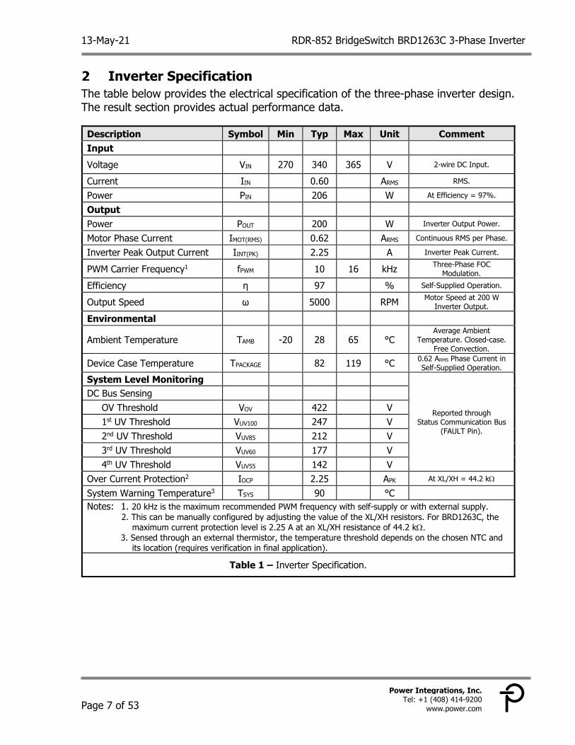
Inverter Specification The table below provides the electrical specification of the three-phase inverter design. The result section provides actual performance data.
Description Symbol Min Typ Max Unit Comment Input
Voltage VIN 270 340 365 V 2-wire DC Input.
Current IIN 0.60 ARMS RMS.
Power PIN 206 W At Efficiency = 97%.
Output
Power POUT 200 W Inverter Output Power.
Motor Phase Current IMOT(RMS) 0.62 ARMS Continuous RMS per Phase.
Inverter Peak Output Current IINT(PK) 2.25 A Inverter Peak Current.
PWM Carrier Frequency1 fPWM 10 16 kHz Three-Phase FOC Modulation.
Efficiency η 97 % Self-Supplied Operation.
Output Speed ω 5000 RPM Motor Speed at 200 W Inverter Output.
Environmental
Ambient Temperature TAMB -20 28 65 °C Average Ambient
Temperature. Closed-case. Free Convection.
Device Case Temperature TPACKAGE 82 119 °C 0.62 ARMS Phase Current in Self-Supplied Operation.
System Level Monitoring
Reported through Status Communication Bus
(FAULT Pin).
DC Bus Sensing OV Threshold VOV 422 V 1st UV Threshold VUV100 247 V 2nd UV Threshold VUV85 212 V 3rd UV Threshold VUV60 177 V 4th UV Threshold VUV55 142 V Over Current Protection2 IOCP 2.25 APK At XL/XH = 44.2 k
System Warning Temperature3 TSYS 90 °C Notes: 1. 20 kHz is the maximum recommended PWM frequency with self-supply or with external supply. 2. This can be manually configured by adjusting the value of the XL/XH resistors. For BRD1263C, the maximum current protection level is 2.25 A at an XL/XH resistance of 44.2 k. 3. Sensed through an external thermistor, the temperature threshold depends on the chosen NTC and its location (requires verification in final application).
Table 1 – Inverter Specification.
RDR-852 BridgeSwitch BRD1263C 3-Phase Inverter 13-May-21
Page 8 of 53
Power Integrations, Inc. Tel: +1 (408) 414-9200 www.power.com
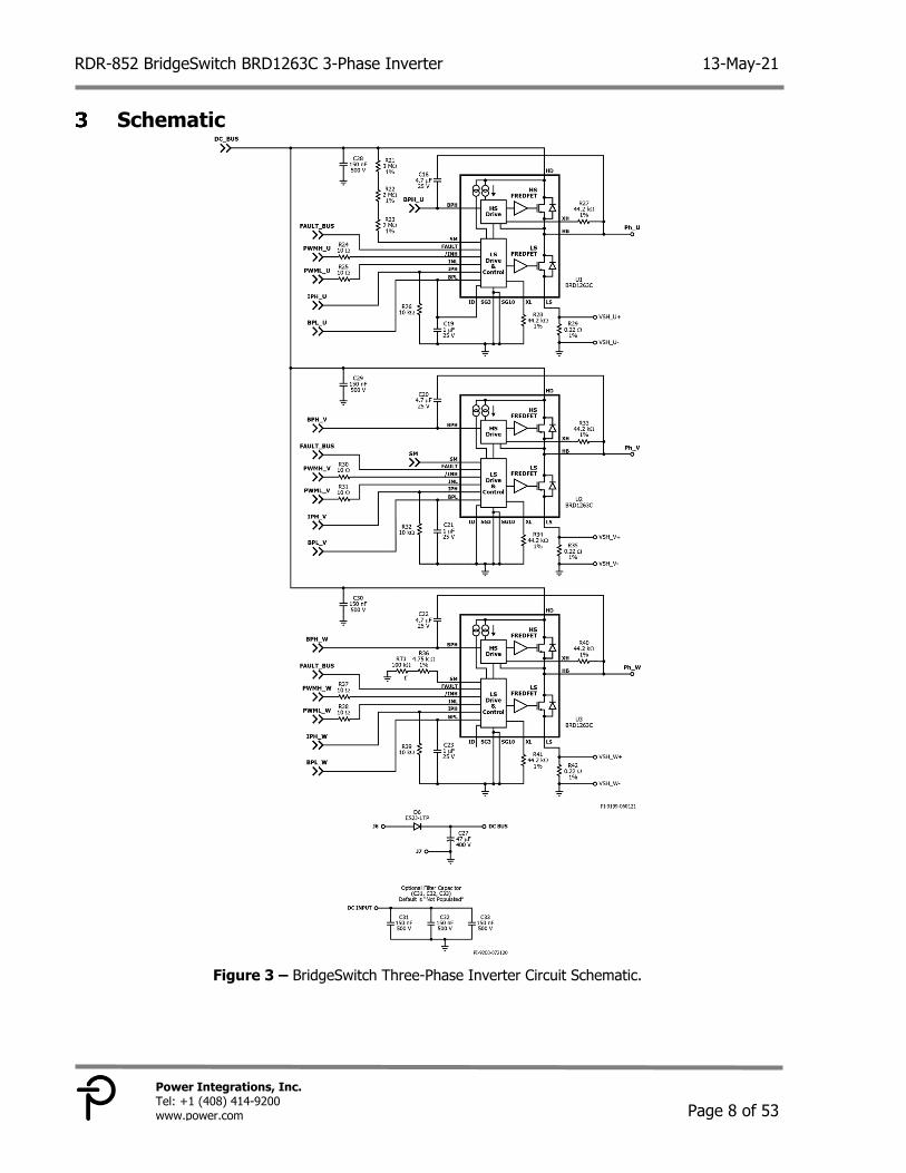
Schematic
Figure 3 – BridgeSwitch Three-Phase Inverter Circuit Schematic.
13-May-21 RDR-852 BridgeSwitch BRD1263C 3-Phase Inverter
Page 9 of 53
Power Integrations, Inc. Tel: +1 (408) 414-9200
www.power.com
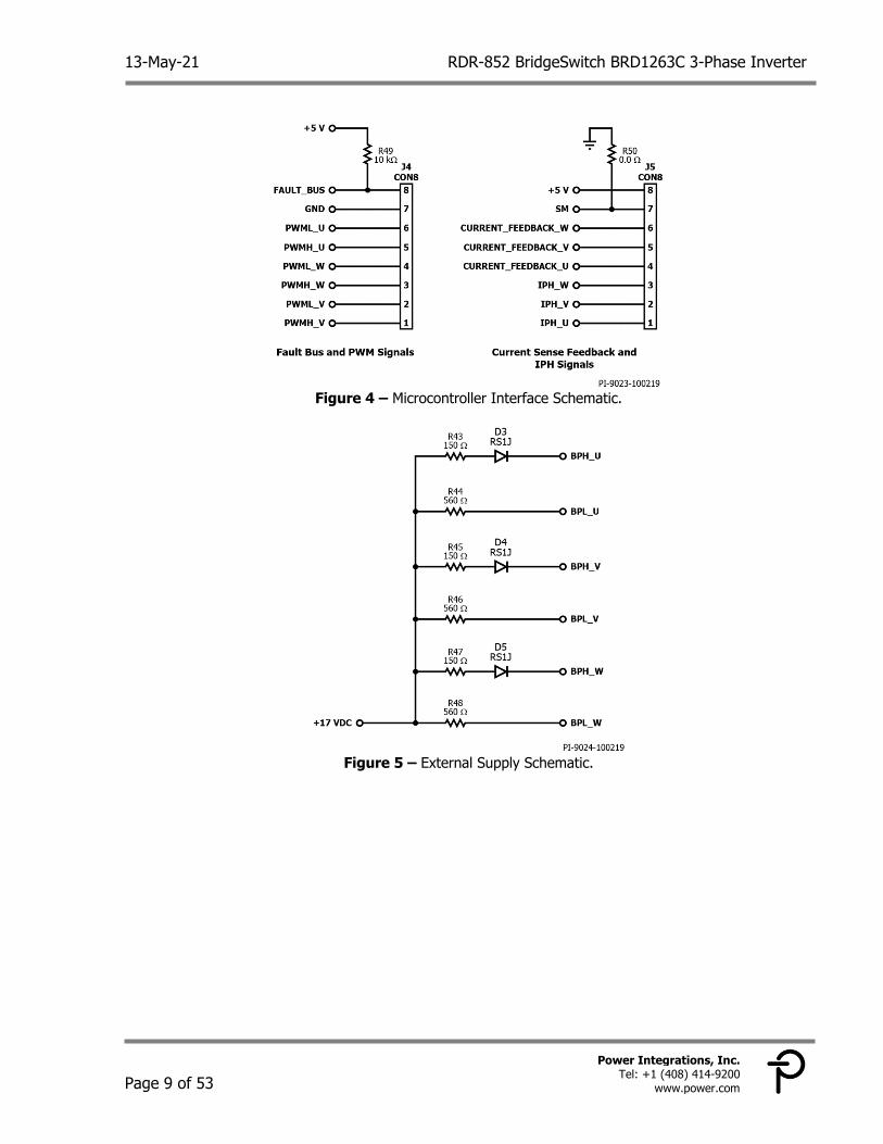
Figure 4 – Microcontroller Interface Schematic.
Figure 5 – External Supply Schematic.
RDR-852 BridgeSwitch BRD1263C 3-Phase Inverter 13-May-21
Page 10 of 53
Power Integrations, Inc. Tel: +1 (408) 414-9200 www.power.com
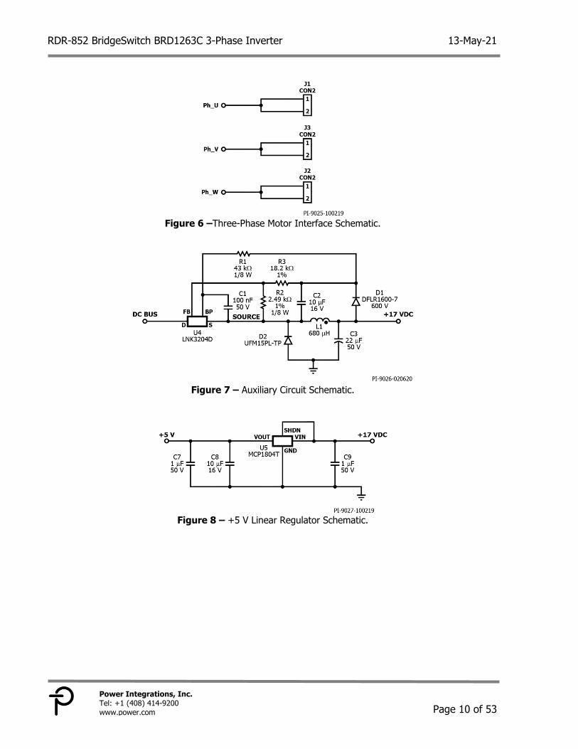
Figure 6 –Three-Phase Motor Interface Schematic.
Figure 7 – Auxiliary Circuit Schematic.
Figure 8 – +5 V Linear Regulator Schematic.
13-May-21 RDR-852 BridgeSwitch BRD1263C 3-Phase Inverter
Page 11 of 53
Power Integrations, Inc. Tel: +1 (408) 414-9200
www.power.com
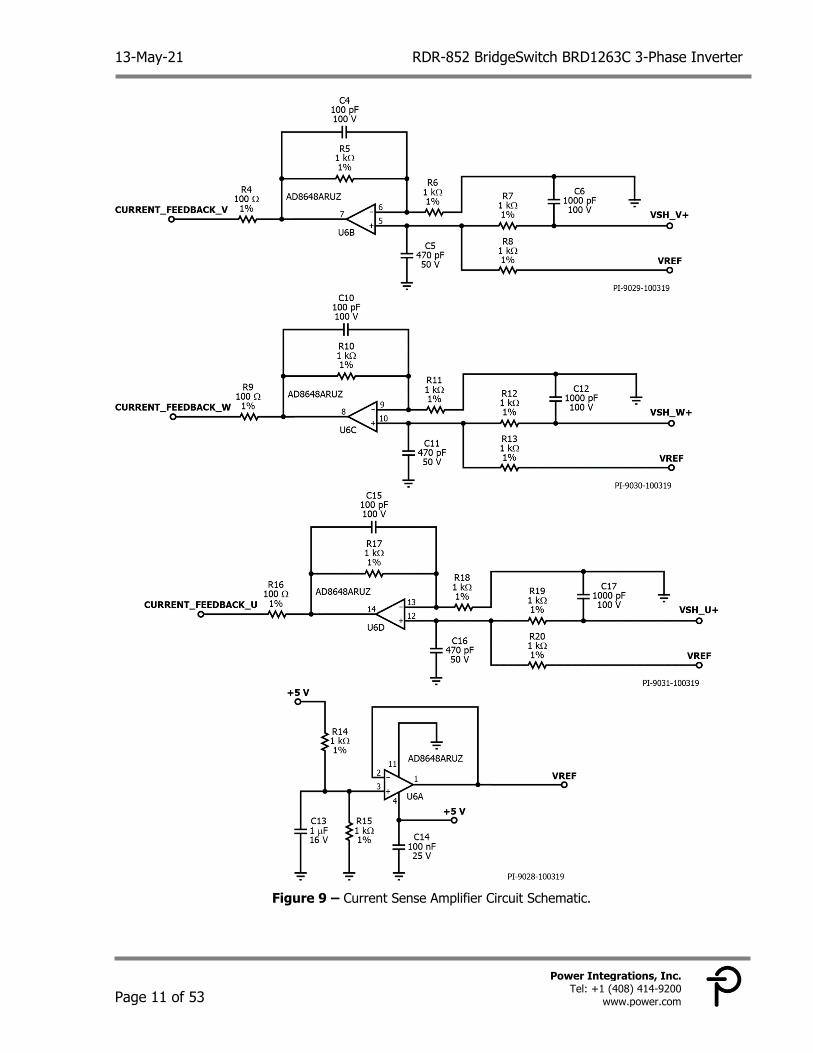
Figure 9 – Current Sense Amplifier Circuit Schematic.
RDR-852 BridgeSwitch BRD1263C 3-Phase Inverter 13-May-21
Page 12 of 53
Power Integrations, Inc. Tel: +1 (408) 414-9200 www.power.com
Circuit Description The overall schematic shows a three-phase inverter utilizing three BridgeSwitch BRD1263C devices. The circuit design drives a high-voltage, three-phase, brushless DC (BLDC) motor utilizing field-oriented control (FOC) for driving the motor. The BridgeSwitch IC combines two 600 V, N-channel power FREDFETs with their corresponding gate drivers into a low profile surface mount package. The BridgeSwitch power FREDFET features an ultra-soft, fast recovery diode ideally suited for inverter drives. Both drivers are fully self-supplied eliminating the need for the system power supply to provide gate drive power. A LinkSwitch-TN2 LNK3204D device in a high-voltage buck converter configuration provides an optional +17 V supply for the BridgeSwitch device (external bias) and input DC voltage for the +5 V linear regulator that supplies the current sense amplifier circuit. In addition, the BridgeSwitch IC incorporates internal fault protection and system level monitoring. Internal fault protection includes cycle-by-cycle current limit for both FREDFETs and a two level thermal overload protection. On the other hand, system level monitoring includes high-voltage DC bus sensing with multi-level undervoltage thresholds and one overvoltage threshold. The BridgeSwitch IC can also be configured using external sensors such as a thermistor for system temperature monitoring. A single wire open drain bus communicates all detected fault or change of status to the system microcontroller.
Three-Phase BridgeSwitch Inverter The three BridgeSwitch devices U1, U2, and U3 form the three-phase inverter. The output of the inverter connects to the three-phase BLDC motor through connectors J1, J2, and J3.
Input Stage The input stage consists of terminals J6 and J7, input diode D6, and bulk capacitor C27. Terminals J6 (positive terminal) and J7 (negative terminal) serve as connectors for the high-voltage DC bus. The bulk capacitor C27 minimizes the path for the high-voltage DC input from the supply to the board. It is protected by input diode D6 from reversed DC voltage in the case of the DC input connections being swapped.
BridgeSwitch Bias Supply Capacitors C19, C21, and C23 provide self-supply decoupling for the integrated low-side controller and gate driver. An internal high-voltage current source recharges these capacitors as soon as the voltage level starts to dip. On the other hand, capacitors C18, C20, and C22 provide self-supply decoupling for the integrated high-side controller and gate driver. Internal high-voltage current sources recharge these capacitors whenever the half-bridge point of the respective device drops to the low-side source voltage level (i.e. the low-side FREDFET turns on).
13-May-21 RDR-852 BridgeSwitch BRD1263C 3-Phase Inverter
Page 13 of 53
Power Integrations, Inc. Tel: +1 (408) 414-9200
www.power.com
PWM Input Input PWM signals PWML_U, PWMH_U, PWML_V, PWMH_V, PWML_W, PWMH_W, control the switching states of the integrated high-side and low-side power FREDFETs. The system microcontroller provides the required PWM signal and desired switching frequency.
Cycle-by-Cycle Current Limit Resistors R28, R34, R41, R27, R33, and R40 set the cycle-by-cycle current limit level for the integrated low-side and high-side power FREDFETs. A selected value of 44.2 kΩ sets the current limit to 100% of the default level or 2.25 APK.
System Underoltage (UV) and Overvoltage (OV) Protection The BridgeSwitch device (U1) monitors the DC bus voltage through resistors R21 (3 MΩ), R22 (2 MΩ), and R23 (2 MΩ). The combined resistance of 7 MΩ sets the undervoltage thresholds to 247 V, 212 V, 177 V, and 142 V. The bus overvoltage threshold is at 422 V. The FAULT pin reports any detected bus voltage fault condition.
System Level Temperature and Monitoring The BridgeSwitch device (U3) monitors the system temperature through thermistor RT1 connected to the SM pin. Resistor R36 tunes the threshold for a system level fault of 90 °C. The device reports a detected status change of the externally set system level temperature through the FAULT pin.
Fault Bus The BridgeSwitch devices (U1, U2, and U3) report any detected internal and system status change through pin 8 of connector J4. The system microcontroller can take action in accordance to the status update reported by the device. Such action could be for instance inverter shutdown, latch, restart, warning, etc.
Device ID Each BRD1263C assigns itself a unique device ID through the connection of pin 11 (ID pin). The pin can be floating, connected to the SG pin, or connected to the BPL pin. The device ID allows the specific device flagging a fault to communicate its physical location to the system microcontroller.
Microcontroller (MCU) Interface Connectors J4 and J5 serve as an interface between the system microcontroller and the BridgeSwitch three-phase inverter which contains the following signals: FAULT_BUS – Pin dedicated for fault reporting of all BridgeSwitch devices. GND – Common ground interface between the microcontroller and the inverter
board. PWMH_U, PWML_U, PWMH_V, PWML_V, PWMH_W, and PWML_W – PWM
input signal interface from the system microcontroller to the BridgeSwitch device.
RDR-852 BridgeSwitch BRD1263C 3-Phase Inverter 13-May-21
Page 14 of 53
Power Integrations, Inc. Tel: +1 (408) 414-9200 www.power.com
+5 V – Voltage supply pin for the microcontroller as needed. SM – Configurable system monitoring pin for the BridgeSwitch device (U2). Curr_fdbkU, Curr_fdbkV, Curr_fdbkW – Current feedback information needed
by the microcontroller (MCU). This signal directly comes from the inverter current sense resistor passing through the current sense amplifier circuit.
IPH_U, IPH_V, IPH_W – Instantaneous phase current information of the low-side power FREDFET Drain-to-Source current of each BridgeSwitch device coming from the IPH pin.
External Supply Components R43, R44, R45, R46, R47, R48 and diodes D3, D4, and D5 are responsible for providing external supply to the BridgeSwitch BPL/BPH pin through device U4. External supply operation is optional for applications that require lower inverter no-load input power or operate at elevated ambient temperatures. Otherwise, these resistors and diode components can be depopulated. If depopulated, BPL/BPH supply will be drawn internally through the BridgeSwitch device (self-supply).
Three-Phase Motor Interface Connectors J1, J2, and J3 are mechanical connectors that directly connect the BridgeSwitch three-phase inverter to the BLDC motor.
Auxiliary Power Supply Circuit Device U4 (LNK3204D) is a high-side buck switcher IC responsible for providing optional +17 V supply for the BPL/BPH (external bias) and +5 V linear regulator. It directly steps down the high input DC voltage to the desired low output voltage. For more information about LNK3204D, please refer to the data sheet through the following link: https://ac-dc.power.com/design-support/product-documents/data-sheets/linkswitch-tn2-data-sheet/
+5 V Linear Regulator Device U5 (MCP1804T) is a +5 V linear regulator that provides DC supply to the current sense amplifier circuit. It can also be used to supply an external microcontroller through pin 8 of connector J5.
Current Sense Amplifier Components U6B, U6C, and U6D are current sense amplifiers which receive data from sense resistors R29, R35, and R42. The current information from these sense resistors are offset to 2.5 VDC level in the current sense op-amp output pins. The U6A circuit provides the 2.5 VDC offset reference voltage. The current information from the outputs of U6B, U6C, and U6D are sent to the microcontroller (MCU) which modulates the PWM input to the BridgeSwitch inverter maintaining the desired power and RPM. Note: U6A, U6B, U6C, and U6D are op-amps in one IC package (Quad op-amp, U6)

13-May-21 RDR-852 BridgeSwitch BRD1263C 3-Phase Inverter
Page 15 of 53
Power Integrations, Inc. Tel: +1 (408) 414-9200
www.power.com
Printed Circuit Board Layout
Figure 10 – Printed Circuit Board Layout Top View.
Note: 1. The overall PCB dimension is 95 mm x 75 mm (L x W). 2. The inverter PCB dimension is 64.8 mm x 51.3 mm (L x W) – in black rectangle. 3. PCB Specifications:
Board thickness: 0.047 inches Board material: FR4 Copper weight: 2 oz No. of layers: 2
RDR-852 BridgeSwitch BRD1263C 3-Phase Inverter 13-May-21
Page 16 of 53
Power Integrations, Inc. Tel: +1 (408) 414-9200 www.power.com
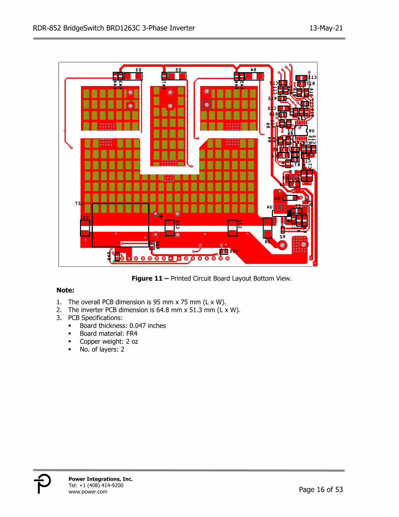
Figure 11 – Printed Circuit Board Layout Bottom View.
Note: 1. The overall PCB dimension is 95 mm x 75 mm (L x W). 2. The inverter PCB dimension is 64.8 mm x 51.3 mm (L x W). 3. PCB Specifications:
Board thickness: 0.047 inches Board material: FR4 Copper weight: 2 oz No. of layers: 2
13-May-21 RDR-852 BridgeSwitch BRD1263C 3-Phase Inverter
Page 17 of 53
Power Integrations, Inc. Tel: +1 (408) 414-9200
www.power.com
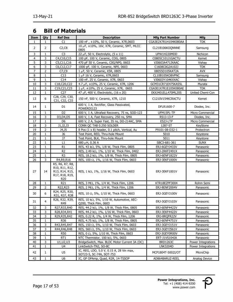
Bill of Materials Item Qty Ref Des Description Mfg Part Number Mfg
1 1 C1 100 nF , ±10%, 50 V, Ceramic, X7R,0603 CGA3E2X7R1H104K080AA TDK
2 2 C2,C8 10 F, ±10%, 16V, X7R, Ceramic, SMT, MLCC 0805 CL21B106KOQNNNE Samsung
3 1 C3 22 F, 50 V, Electrolytic, (5 x 11) UPW1H220MDD Nichicon 4 3 C4,C10,C15 100 pF, 100 V, Ceramic, COG, 0805 C0805C101J1GACTU Kemet 5 3 C5,C11,C16 470 pF 50 V, Ceramic, C0G/NP0, 0603 VJ0603A471JXAAC Vishay 6 3 C6,C12,C17 1000 pF, 100 V, Ceramic, NP0, 0603 C1608C0G2A102J TDK 7 2 C7,C9 1 F, 50 V, Ceramic, X5R, 0805 08055D105KAT2A AVX 8 1 C13 1 F 16 V, Ceramic, X7R,0603 CL10B105KO8VPNC Samsung 9 1 C14 100 nF, 25 V, Ceramic, X7R, 0603 VJ0603Y104KXXAC Vishay 10 3 C18,C20,C22 4.7 F, ±10%, 25 V, Ceramic, X7R, 1206 GCM31CR71E475KA55L Murata 11 3 C19,C21,C23 1 F, ±10%, 25 V, Ceramic, X7R, 0603 CGA3E1X7R1E105K080AE TDK 12 1 C27 47 μF, 400 V, Electrolytic, (16 x 20) EKXJ401ELL470ML20S United Chemi-Con
13 6 C28, C29, C30, C31, C32, C33 150 nF, 500 V, Ceramic, X7R, 1210 C1210V154KCRACTU Kemet
14 1 D1 600 V, 1 A, Rectifier, Glass Passivated, POWERDI123 DFLR1600-7 Diodes, Inc.
15 1 D2 600 V, 1 A, Ultrafast Recovery, 75 ns, SOD-123 UFM15PL-TP Micro Commercial 16 3 D3,D4,D5 600 V, 1 A, Fast Recovery, 250 ns, SMA RS1J-13-F Diodes, Inc. 17 1 D6 600 V, 2 A, Super Fast, 35 ns, DO-214AC, SMA ES2J-LTP Micro Commercial 18 3 J1,J2,J3 CONN QC TAB 0.250 SOLDER 1287-ST KeyStone 19 2 J4,J5 8 Pos (1 x 8) header, 0.1 pitch, Vertical, Au P9101-08-D32-1 Protectron 20 1 J6 Test Point, RED, Thru-hole Mount 5010 Keystone 21 1 J7 Test Point, BLK, Thru-hole Mount 5011 Keystone 22 1 L1 680 H, 0.36 A SBC3-681-361 SUNX 23 1 R1 RES, 43 k, 5%, 1/8 W, Thick Film, 0805 ERJ-6GEYJ433V Panasonic 24 1 R2 RES, 2.49 k, 1%, 1/10 W, Thick Film, 0402 ERJ-2RKF2491X Panasonic 25 1 R3 RES, 18.2 k, 1%, 1/8 W, Thick Film, 0805 ERJ-6ENF1822V Panasonic 26 3 R4,R9,R16 RES, 100 , 1%, 1/16 W, Thick Film, 0603 ERJ-3EKF1000V Panasonic
27 14
R5, R6, R7, R8, R10, R11, R12, R13, R14, R15, R17, R18, R19,
R20
RES, 1 k, 1%, 1/16 W, Thick Film, 0603 ERJ-3EKF1001V Panasonic
28 1 R21 RES, 3 M, 1%, 1/4 W, Thick Film, 1206 KTR18EZPF3004 Rohm Semi 29 2 R22,R23 RES, 2 M, 1%, 1/4 W, Thick Film, 1206 ERJ-8ENF2004V Panasonic
30 6 R24, R25, R30, R31, R37, R38 RES, 10 , 5%, 1/10 W, Thick Film, 0603 ERJ-3GEYJ100V Panasonic
31 4 R26, R32, R39, R49
RES, 10 k, 5%, 1/10 W, Automotive, AEC-Q200, Thick Film, 0603 ERJ-3GEYJ103V Panasonic
32 3 R27,R33,R40 RES, 44.2 k, 1%, 1/8 W, Thick Film, 0805 ERJ-6ENF4422V Panasonic 33 3 R28,R34,R41 RES, 44.2 k, 1%, 1/16 W, Thick Film, 0603 ERJ-3EKF4422V Panasonic 34 3 R29,R35,R42 RES, 0.22 R, 1%, 1/4 W, Thick Film, 1206 ERJ-8RQFR22V Panasonic 35 1 R36 RES, 4.75 k, 1%, 1/8 W, Thick Film, 0805 ERJ-6ENF4751V Panasonic 36 3 R43,R45,R47 RES, 150 , 5%, 1/10 W, Thick Film, 0603 ERJ-3GEYJ151V Panasonic 37 3 R44,R46,R48 RES, 560 , 5%, 1/10 W, Thick Film, 0603 ERJ-3GEYJ561V Panasonic 38 1 R50 RES, 0 , 5%, 1/10 W, Thick Film, 0603 ERJ-3GEY0R00V Panasonic 39 1 RT1 NTC Thermistor, 100 k, 5%, 0603 ERT-J1VS104JA Panasonic 40 3 U1,U2,U3 BridgeSwitch, Max. BLDC Motor Current 3A (DC) BRD1263C Power Integrations 41 1 U4 LinkSwitch-TN2, SO-8C LNK3204D Power Integrations
42 1 U5 IC, REG, LDO, 5.0 V, 0.15 A, 28 Vin max, SOT23-5, SC-74A, SOT-753 MCP1804T-5002I/OT MicroChip
43 1 U6 IC, GP OPAmp, Quad, R2R, 14-TSSOP AD8648ARUZ-REEL Analog Device
RDR-852 BridgeSwitch BRD1263C 3-Phase Inverter 13-May-21
Page 18 of 53
Power Integrations, Inc. Tel: +1 (408) 414-9200 www.power.com
Performance Data This section presents the waveform plots and performance data of the BridgeSwitch inverter. The high-voltage (VBUS) level is 340 VDC unless stated otherwise. Light load measurements describe the inverter operating with no mechanical brake load applied to the motor. Full load operation describes the inverter operating at 200 W output power (refer to Appendix for the details on the method used to measure the output power of a three-phase inverter). All measurements were performed at 10 kHz PWM frequency, 28°C average ambient temperature, and three-phase field-oriented control (three-phase FOC) type of modulation.
Start-Up Operation
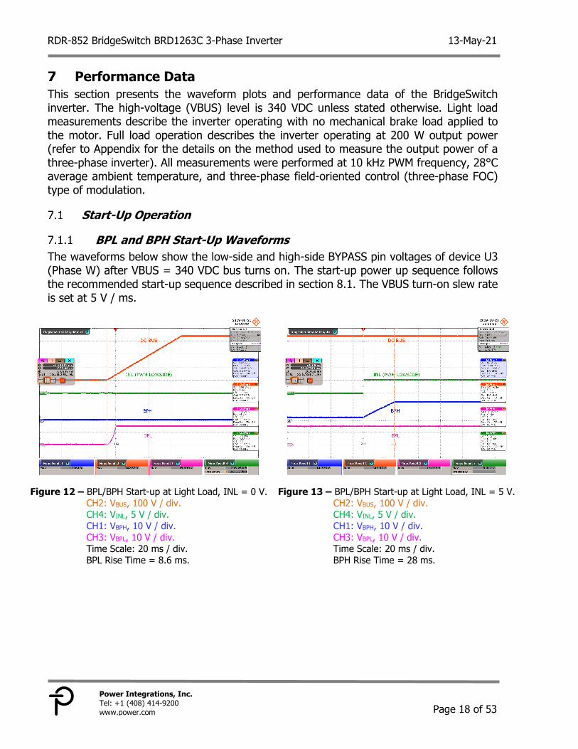
BPL and BPH Start-Up Waveforms The waveforms below show the low-side and high-side BYPASS pin voltages of device U3 (Phase W) after VBUS = 340 VDC bus turns on. The start-up power up sequence follows the recommended start-up sequence described in section 8.1. The VBUS turn-on slew rate is set at 5 V / ms.
Figure 12 – BPL/BPH Start-up at Light Load, INL = 0 V.
CH2: VBUS, 100 V / div. CH4: VINL, 5 V / div. CH1: VBPH, 10 V / div. CH3: VBPL, 10 V / div. Time Scale: 20 ms / div. BPL Rise Time = 8.6 ms.
Figure 13 – BPL/BPH Start-up at Light Load, INL = 5 V. CH2: VBUS, 100 V / div. CH4: VINL, 5 V / div. CH1: VBPH, 10 V / div. CH3: VBPL, 10 V / div. Time Scale: 20 ms / div. BPH Rise Time = 28 ms.
13-May-21 RDR-852 BridgeSwitch BRD1263C 3-Phase Inverter
Page 19 of 53
Power Integrations, Inc. Tel: +1 (408) 414-9200
www.power.com
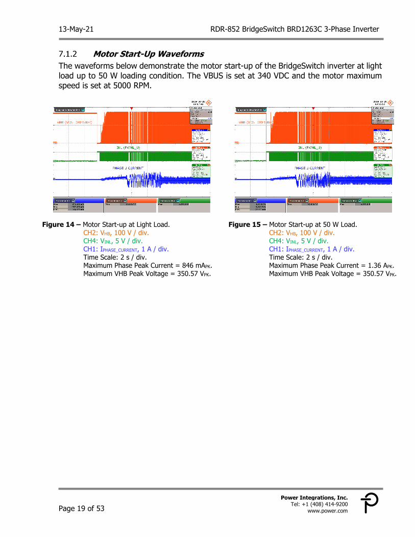
Motor Start-Up Waveforms The waveforms below demonstrate the motor start-up of the BridgeSwitch inverter at light load up to 50 W loading condition. The VBUS is set at 340 VDC and the motor maximum speed is set at 5000 RPM.
Figure 14 – Motor Start-up at Light Load.
CH2: VHB, 100 V / div. CH4: VINL, 5 V / div. CH1: IPHASE_CURRENT, 1 A / div. Time Scale: 2 s / div. Maximum Phase Peak Current = 846 mAPK. Maximum VHB Peak Voltage = 350.57 VPK.
Figure 15 – Motor Start-up at 50 W Load. CH2: VHB, 100 V / div. CH4: VINL, 5 V / div. CH1: IPHASE_CURRENT, 1 A / div. Time Scale: 2 s / div. Maximum Phase Peak Current = 1.36 APK. Maximum VHB Peak Voltage = 350.57 VPK.
RDR-852 BridgeSwitch BRD1263C 3-Phase Inverter 13-May-21
Page 20 of 53
Power Integrations, Inc. Tel: +1 (408) 414-9200 www.power.com
Steady-State Operation
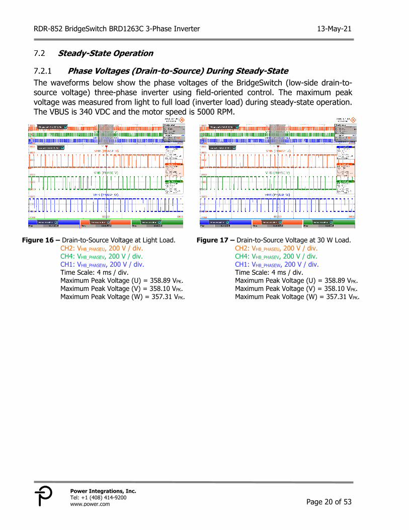
Phase Voltages (Drain-to-Source) During Steady-State The waveforms below show the phase voltages of the BridgeSwitch (low-side drain-to-source voltage) three-phase inverter using field-oriented control. The maximum peak voltage was measured from light to full load (inverter load) during steady-state operation. The VBUS is 340 VDC and the motor speed is 5000 RPM.
Figure 16 – Drain-to-Source Voltage at Light Load.
CH2: VHB_PHASEU, 200 V / div. CH4: VHB_PHASEV, 200 V / div. CH1: VHB_PHASEW, 200 V / div. Time Scale: 4 ms / div. Maximum Peak Voltage (U) = 358.89 VPK. Maximum Peak Voltage (V) = 358.10 VPK. Maximum Peak Voltage (W) = 357.31 VPK.
Figure 17 – Drain-to-Source Voltage at 30 W Load. CH2: VHB_PHASEU, 200 V / div. CH4: VHB_PHASEV, 200 V / div. CH1: VHB_PHASEW, 200 V / div. Time Scale: 4 ms / div. Maximum Peak Voltage (U) = 358.89 VPK. Maximum Peak Voltage (V) = 358.10 VPK. Maximum Peak Voltage (W) = 357.31 VPK.
13-May-21 RDR-852 BridgeSwitch BRD1263C 3-Phase Inverter
Page 21 of 53
Power Integrations, Inc. Tel: +1 (408) 414-9200
www.power.com
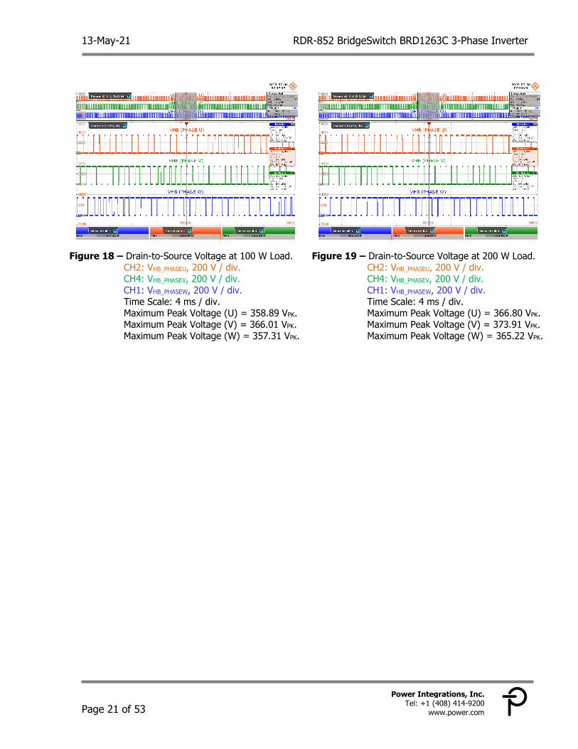
Figure 18 – Drain-to-Source Voltage at 100 W Load.
CH2: VHB_PHASEU, 200 V / div. CH4: VHB_PHASEV, 200 V / div. CH1: VHB_PHASEW, 200 V / div. Time Scale: 4 ms / div. Maximum Peak Voltage (U) = 358.89 VPK. Maximum Peak Voltage (V) = 366.01 VPK. Maximum Peak Voltage (W) = 357.31 VPK.
Figure 19 – Drain-to-Source Voltage at 200 W Load. CH2: VHB_PHASEU, 200 V / div. CH4: VHB_PHASEV, 200 V / div. CH1: VHB_PHASEW, 200 V / div. Time Scale: 4 ms / div. Maximum Peak Voltage (U) = 366.80 VPK. Maximum Peak Voltage (V) = 373.91 VPK. Maximum Peak Voltage (W) = 365.22 VPK.
RDR-852 BridgeSwitch BRD1263C 3-Phase Inverter 13-May-21
Page 22 of 53
Power Integrations, Inc. Tel: +1 (408) 414-9200 www.power.com
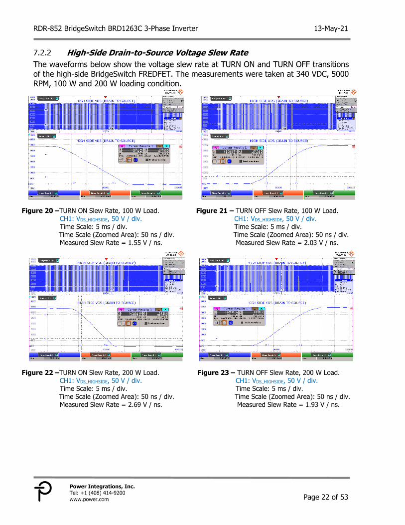
High-Side Drain-to-Source Voltage Slew Rate The waveforms below show the voltage slew rate at TURN ON and TURN OFF transitions of the high-side BridgeSwitch FREDFET. The measurements were taken at 340 VDC, 5000 RPM, 100 W and 200 W loading condition.
Figure 20 –TURN ON Slew Rate, 100 W Load.
CH1: VDS_HIGHSIDE, 50 V / div. Time Scale: 5 ms / div.
Time Scale (Zoomed Area): 50 ns / div. Measured Slew Rate = 1.55 V / ns.
Figure 21 – TURN OFF Slew Rate, 100 W Load. CH1: VDS_HIGHSIDE, 50 V / div. Time Scale: 5 ms / div.
Time Scale (Zoomed Area): 50 ns / div. Measured Slew Rate = 2.03 V / ns.
Figure 22 –TURN ON Slew Rate, 200 W Load.
CH1: VDS_HIGHSIDE, 50 V / div. Time Scale: 5 ms / div.
Time Scale (Zoomed Area): 50 ns / div. Measured Slew Rate = 2.69 V / ns.
Figure 23 – TURN OFF Slew Rate, 200 W Load. CH1: VDS_HIGHSIDE, 50 V / div. Time Scale: 5 ms / div.
Time Scale (Zoomed Area): 50 ns / div. Measured Slew Rate = 1.93 V / ns.
13-May-21 RDR-852 BridgeSwitch BRD1263C 3-Phase Inverter
Page 23 of 53
Power Integrations, Inc. Tel: +1 (408) 414-9200
www.power.com
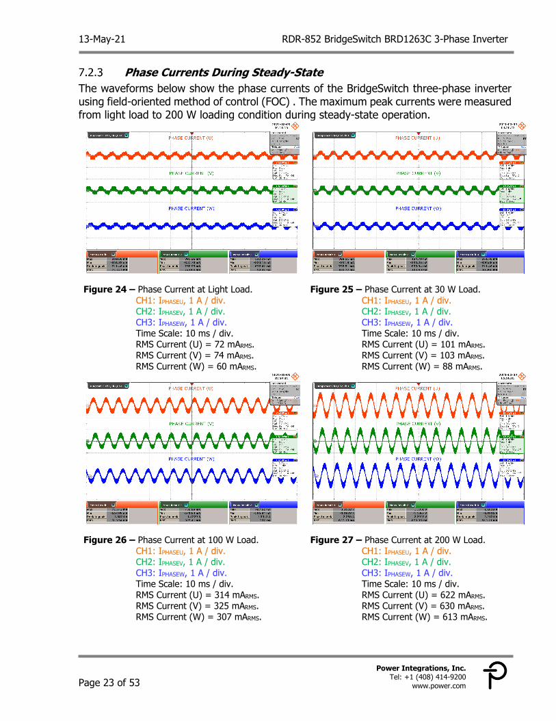
Phase Currents During Steady-State The waveforms below show the phase currents of the BridgeSwitch three-phase inverter using field-oriented method of control (FOC) . The maximum peak currents were measured from light load to 200 W loading condition during steady-state operation.
Figure 24 – Phase Current at Light Load.
CH1: IPHASEU, 1 A / div. CH2: IPHASEV, 1 A / div. CH3: IPHASEW, 1 A / div. Time Scale: 10 ms / div. RMS Current (U) = 72 mARMS. RMS Current (V) = 74 mARMS. RMS Current (W) = 60 mARMS.
Figure 25 – Phase Current at 30 W Load. CH1: IPHASEU, 1 A / div. CH2: IPHASEV, 1 A / div. CH3: IPHASEW, 1 A / div. Time Scale: 10 ms / div. RMS Current (U) = 101 mARMS. RMS Current (V) = 103 mARMS. RMS Current (W) = 88 mARMS.
Figure 26 – Phase Current at 100 W Load.
CH1: IPHASEU, 1 A / div. CH2: IPHASEV, 1 A / div. CH3: IPHASEW, 1 A / div. Time Scale: 10 ms / div. RMS Current (U) = 314 mARMS. RMS Current (V) = 325 mARMS. RMS Current (W) = 307 mARMS.
Figure 27 – Phase Current at 200 W Load. CH1: IPHASEU, 1 A / div. CH2: IPHASEV, 1 A / div. CH3: IPHASEW, 1 A / div. Time Scale: 10 ms / div. RMS Current (U) = 622 mARMS. RMS Current (V) = 630 mARMS. RMS Current (W) = 613 mARMS.
RDR-852 BridgeSwitch BRD1263C 3-Phase Inverter 13-May-21
Page 24 of 53
Power Integrations, Inc. Tel: +1 (408) 414-9200 www.power.com
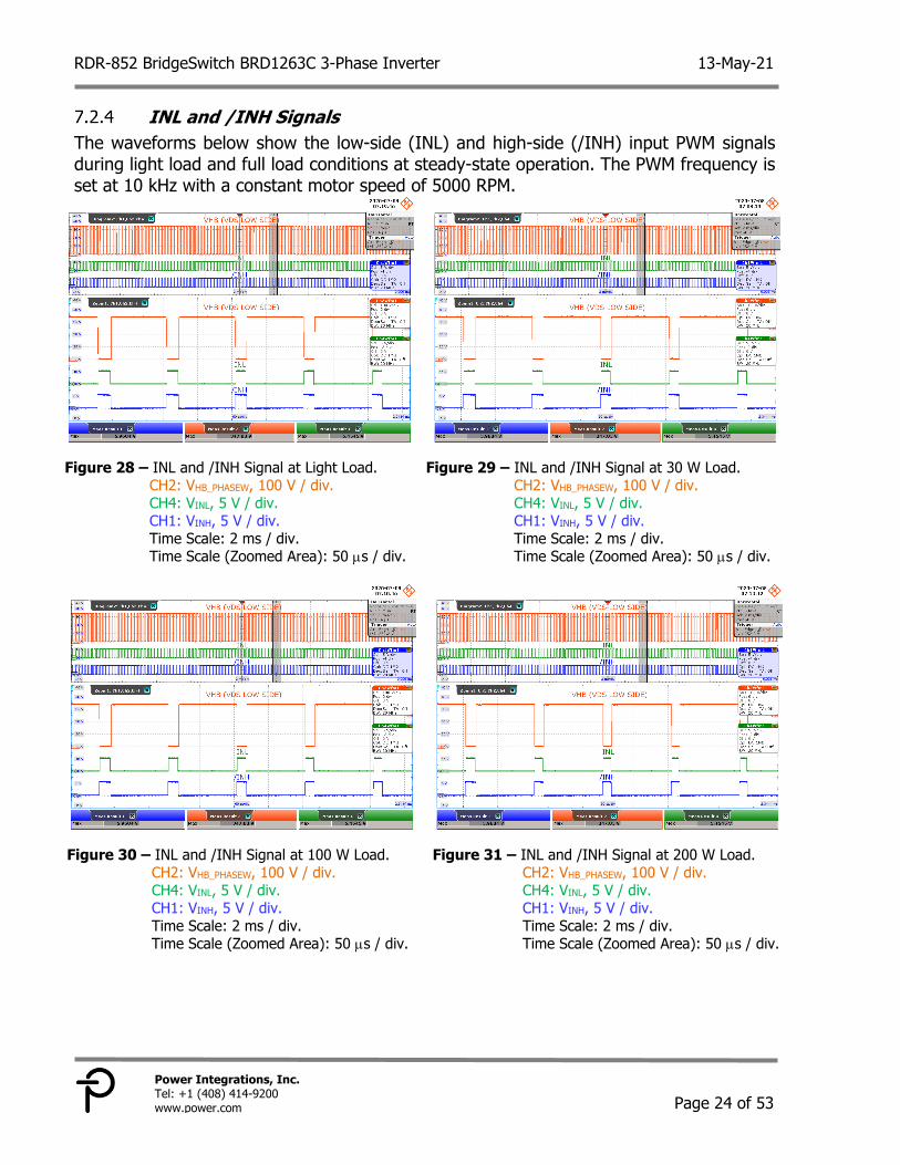
INL and /INH Signals The waveforms below show the low-side (INL) and high-side (/INH) input PWM signals during light load and full load conditions at steady-state operation. The PWM frequency is set at 10 kHz with a constant motor speed of 5000 RPM.
Figure 28 – INL and /INH Signal at Light Load.
CH2: VHB_PHASEW, 100 V / div. CH4: VINL, 5 V / div. CH1: VINH, 5 V / div. Time Scale: 2 ms / div. Time Scale (Zoomed Area): 50 s / div.
Figure 29 – INL and /INH Signal at 30 W Load. CH2: VHB_PHASEW, 100 V / div. CH4: VINL, 5 V / div. CH1: VINH, 5 V / div. Time Scale: 2 ms / div. Time Scale (Zoomed Area): 50 s / div.
Figure 30 – INL and /INH Signal at 100 W Load.
CH2: VHB_PHASEW, 100 V / div. CH4: VINL, 5 V / div. CH1: VINH, 5 V / div. Time Scale: 2 ms / div. Time Scale (Zoomed Area): 50 s / div.
Figure 31 – INL and /INH Signal at 200 W Load. CH2: VHB_PHASEW, 100 V / div. CH4: VINL, 5 V / div. CH1: VINH, 5 V / div. Time Scale: 2 ms / div. Time Scale (Zoomed Area): 50 s / div.
13-May-21 RDR-852 BridgeSwitch BRD1263C 3-Phase Inverter
Page 25 of 53
Power Integrations, Inc. Tel: +1 (408) 414-9200
www.power.com
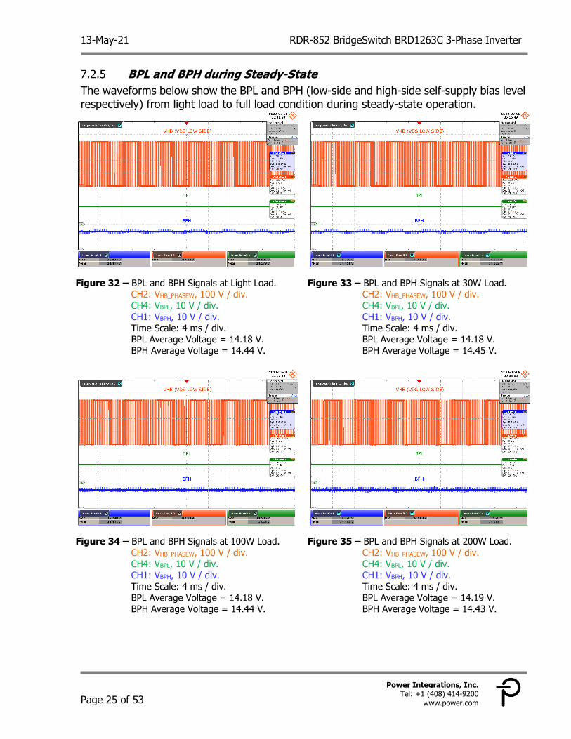
BPL and BPH during Steady-State The waveforms below show the BPL and BPH (low-side and high-side self-supply bias level respectively) from light load to full load condition during steady-state operation.
Figure 32 – BPL and BPH Signals at Light Load.
CH2: VHB_PHASEW, 100 V / div. CH4: VBPL, 10 V / div. CH1: VBPH, 10 V / div. Time Scale: 4 ms / div. BPL Average Voltage = 14.18 V. BPH Average Voltage = 14.44 V.
Figure 33 – BPL and BPH Signals at 30W Load. CH2: VHB_PHASEW, 100 V / div. CH4: VBPL, 10 V / div. CH1: VBPH, 10 V / div. Time Scale: 4 ms / div. BPL Average Voltage = 14.18 V. BPH Average Voltage = 14.45 V.
Figure 34 – BPL and BPH Signals at 100W Load.
CH2: VHB_PHASEW, 100 V / div. CH4: VBPL, 10 V / div. CH1: VBPH, 10 V / div. Time Scale: 4 ms / div. BPL Average Voltage = 14.18 V. BPH Average Voltage = 14.44 V.
Figure 35 – BPL and BPH Signals at 200W Load. CH2: VHB_PHASEW, 100 V / div. CH4: VBPL, 10 V / div. CH1: VBPH, 10 V / div. Time Scale: 4 ms / div. BPL Average Voltage = 14.19 V. BPH Average Voltage = 14.43 V.
RDR-852 BridgeSwitch BRD1263C 3-Phase Inverter 13-May-21
Page 26 of 53
Power Integrations, Inc. Tel: +1 (408) 414-9200 www.power.com
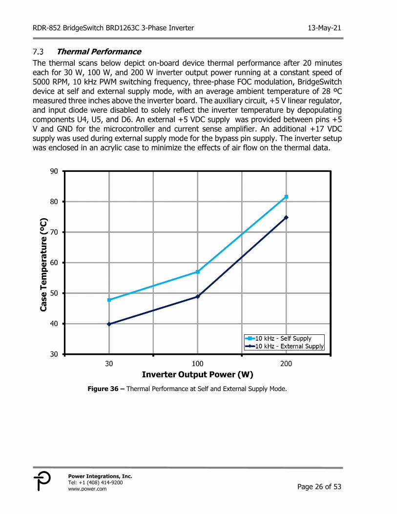
Thermal Performance The thermal scans below depict on-board device thermal performance after 20 minutes each for 30 W, 100 W, and 200 W inverter output power running at a constant speed of 5000 RPM, 10 kHz PWM switching frequency, three-phase FOC modulation, BridgeSwitch device at self and external supply mode, with an average ambient temperature of 28 ºC measured three inches above the inverter board. The auxiliary circuit, +5 V linear regulator, and input diode were disabled to solely reflect the inverter temperature by depopulating components U4, U5, and D6. An external +5 VDC supply was provided between pins +5 V and GND for the microcontroller and current sense amplifier. An additional +17 VDC supply was used during external supply mode for the bypass pin supply. The inverter setup was enclosed in an acrylic case to minimize the effects of air flow on the thermal data.
Figure 36 – Thermal Performance at Self and External Supply Mode.

13-May-21 RDR-852 BridgeSwitch BRD1263C 3-Phase Inverter
Page 27 of 53
Power Integrations, Inc. Tel: +1 (408) 414-9200
www.power.com
30 W Loading Condition (95 mA Average Motor Phase Current)
Figure 37 – BridgeSwitch Device Case Temperatures at 30 W Output Power (Self-Supply Mode).
Figure 38 – BridgeSwitch Device Case Temperatures at 30 W Output Power (External Supply Mode).
100 W Loading Condition (315 mA Average Motor Phase Current)
Figure 39 – BridgeSwitch Device Case Temperatures at 100 W Output Power (Self-Supply Mode).
Figure 40 – BridgeSwitch Device Case Temperatures at 100 W Output Power (External Supply Mode).
RDR-852 BridgeSwitch BRD1263C 3-Phase Inverter 13-May-21
Page 28 of 53
Power Integrations, Inc. Tel: +1 (408) 414-9200 www.power.com
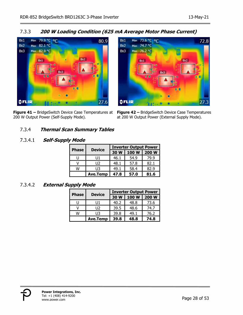
200 W Loading Condition (625 mA Average Motor Phase Current)
Figure 41 – BridgeSwitch Device Case Temperatures at 200 W Output Power (Self-Supply Mode).
Figure 42 – BridgeSwitch Device Case Temperatures at 200 W Output Power (External Supply Mode).
Thermal Scan Summary Tables
Self-Supply Mode
Phase Device Inverter Output Power 30 W 100 W 200 W
U U1 46.1 54.9 79.9 V U2 48.1 57.8 82.1 W U3 49.1 58.4 82.9 Ave.Temp 47.8 57.0 81.6
External Supply Mode
Phase Device Inverter Output Power 30 W 100 W 200 W
U U1 40.2 48.8 73.6 V U2 39.5 48.6 74.7 W U3 39.8 49.1 76.2 Ave.Temp 39.8 48.8 74.8
13-May-21 RDR-852 BridgeSwitch BRD1263C 3-Phase Inverter
Page 29 of 53
Power Integrations, Inc. Tel: +1 (408) 414-9200
www.power.com
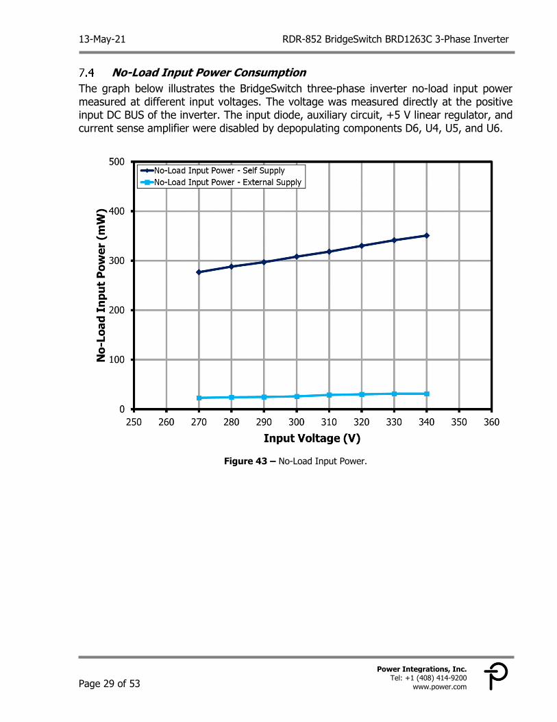
No-Load Input Power Consumption The graph below illustrates the BridgeSwitch three-phase inverter no-load input power measured at different input voltages. The voltage was measured directly at the positive input DC BUS of the inverter. The input diode, auxiliary circuit, +5 V linear regulator, and current sense amplifier were disabled by depopulating components D6, U4, U5, and U6.
Figure 43 – No-Load Input Power.
RDR-852 BridgeSwitch BRD1263C 3-Phase Inverter 13-May-21
Page 30 of 53
Power Integrations, Inc. Tel: +1 (408) 414-9200 www.power.com
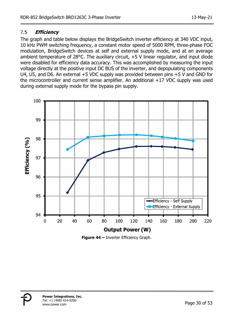
Efficiency The graph and table below displays the BridgeSwitch inverter efficiency at 340 VDC input, 10 kHz PWM switching frequency, a constant motor speed of 5000 RPM, three-phase FOC modulation, BridgeSwitch devices at self and external supply mode, and at an average ambient temperature of 28°C. The auxiliary circuit, +5 V linear regulator, and input diode were disabled for efficiency data accuracy. This was accomplished by measuring the input voltage directly at the positive input DC BUS of the inverter, and depopulating components U4, U5, and D6. An external +5 VDC supply was provided between pins +5 V and GND for the microcontroller and current sense amplifier. An additional +17 VDC supply was used during external supply mode for the bypass pin supply.
Figure 44 – Inverter Efficiency Graph.
13-May-21 RDR-852 BridgeSwitch BRD1263C 3-Phase Inverter
Page 31 of 53
Power Integrations, Inc. Tel: +1 (408) 414-9200
www.power.com
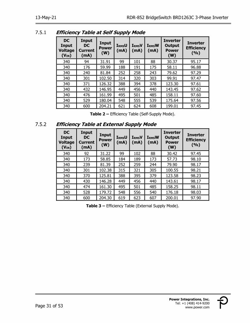
Efficiency Table at Self Supply Mode DC
Input Voltage
(VIN)
Input DC
Current (mA)
Input Power
(W) IRMSU (mA)
IRMSV (mA)
IRMSW (mA)
Inverter Output Power
(W)
Inverter Efficiency
(%)
340 94 31.91 99 101 88 30.37 95.17 340 176 59.99 188 191 175 58.11 96.88 340 240 81.84 252 258 243 79.62 97.29 340 301 102.50 314 320 303 99.91 97.47 340 371 126.32 388 394 378 123.30 97.61 340 432 146.95 449 456 440 143.45 97.62 340 476 161.99 495 501 485 158.11 97.60 340 529 180.04 548 555 539 175.64 97.56 340 600 204.21 621 624 608 199.01 97.45
Table 2 – Efficiency Table (Self-Supply Mode).
Efficiency Table at External Supply Mode DC
Input Voltage
(VIN)
Input DC
Current (mA)
Input Power
(W) IRMSU (mA)
IRMSV (mA)
IRMSW (mA)
Inverter Output Power
(W)
Inverter Efficiency
(%)
340 92 31.22 99 102 88 30.42 97.45 340 173 58.85 184 189 173 57.73 98.10 340 239 81.39 252 259 244 79.90 98.17 340 301 102.38 315 321 305 100.55 98.21 340 370 125.81 388 395 379 123.58 98.23 340 430 146.28 449 456 440 143.61 98.17 340 474 161.30 495 501 485 158.25 98.11 340 528 179.72 548 556 540 176.18 98.03 340 600 204.30 619 623 607 200.01 97.90
Table 3 – Efficiency Table (External Supply Mode).
RDR-852 BridgeSwitch BRD1263C 3-Phase Inverter 13-May-21
Page 32 of 53
Power Integrations, Inc. Tel: +1 (408) 414-9200 www.power.com
Device and System Level Protection / Monitoring
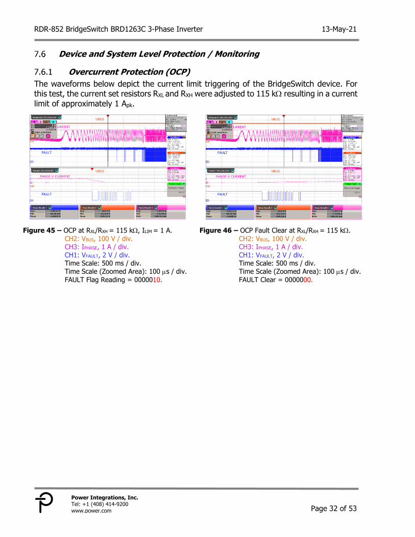
Overcurrent Protection (OCP) The waveforms below depict the current limit triggering of the BridgeSwitch device. For this test, the current set resistors RXL and RXH were adjusted to 115 k resulting in a current limit of approximately 1 Apk.
Figure 45 – OCP at RXL/RXH = 115 k, ILIM = 1 A. CH2: VBUS, 100 V / div. CH3: IPHASE, 1 A / div. CH1: VFAULT, 2 V / div. Time Scale: 500 ms / div. Time Scale (Zoomed Area): 100 s / div. FAULT Flag Reading = 0000010.
Figure 46 – OCP Fault Clear at RXL/RXH = 115 k. CH2: VBUS, 100 V / div. CH3: IPHASE, 1 A / div. CH1: VFAULT, 2 V / div. Time Scale: 500 ms / div. Time Scale (Zoomed Area): 100 s / div. FAULT Clear = 0000000.
13-May-21 RDR-852 BridgeSwitch BRD1263C 3-Phase Inverter
Page 33 of 53
Power Integrations, Inc. Tel: +1 (408) 414-9200
www.power.com
Thermal Warning The waveforms below depict the low-side FREDFET over-temperature warning. A localized external heat source was applied to the device to force temperature rise.
Figure 47 – Thermal Warning at Light Load.
CH3: IPHASE, 1 A / div. CH1: VFAULT, 2 V / div. Time Scale: 10 ms / div. Time Scale (Zoomed Area): 100 s / div. FAULT Flag/Reading = 0000100.
Figure 48 – Thermal Warning at 30 W. CH3: IPHASE, 1 A / div. CH1: VFAULT, 2 V / div. Time Scale: 10 ms / div. Time Scale (Zoomed Area): 100 s / div. FAULT Flag/Reading = 0000100.
Figure 49 – Thermal Warning at 100 W.
CH3: IPHASE, 1 A / div. CH1: VFAULT, 2 V / div. Time Scale: 10 ms / div. Time Scale (Zoomed Area): 100 s / div. FAULT Flag/Reading = 0000100.
Figure 50 – Thermal Warning at 200 W. CH3: IPHASE, 1 A / div. CH1: VFAULT, 2 V / div. Time Scale: 10 ms / div. Time Scale (Zoomed Area): 100 s / div. FAULT Flag/Reading = 0000100.
RDR-852 BridgeSwitch BRD1263C 3-Phase Inverter 13-May-21
Page 34 of 53
Power Integrations, Inc. Tel: +1 (408) 414-9200 www.power.com
Thermal Shutdown The waveform below depicts the low-side FREDFET over-temperature shutdown. A localized external heat source was applied to a single BridgeSwitch device (U2) to force temperature rise while the inverter is running at 100 W loading condition.
Figure 51 – Thermal Shutdown.
CH1: IPHASEU, 2 A / div. CH2: IPHASEV, 2 A / div. CH3: IPHASEW, 2 A / div. CH4: VFAULT, 1 V / div. Time Scale: 100 ms / div. Time Scale (Zoomed FAULT): 100 s / div. FAULT Flag/Reading = 0001000.
13-May-21 RDR-852 BridgeSwitch BRD1263C 3-Phase Inverter
Page 35 of 53
Power Integrations, Inc. Tel: +1 (408) 414-9200
www.power.com
Undervoltage (UV) The test results below demonstrate the integrated bus UV monitoring function and status reporting through the communication bus (FAULT pin). Device U1 senses the bus voltage through resistors R21, R22, and R23.
Figure 52 – UVP, 5000 RPM, No-Load, 340 V to 220 V.
CH2: VBUS, 100 V / div. CH1: VFAULT, 2 V / div. Time Scale: 100 s / div. UV Level = 100%. FAULT Flag Reading = 0100000.
Figure 53 – UVP, 5000 RPM, No-Load, 220 V to 190 V. CH2: VBUS, 100 V / div. CH1: VFAULT, 2 V / div. Time Scale: 100 s / div. UV Level = 85%. FAULT Flag Reading = 0110000.
Figure 54 – UVP, 5000 RPM, No-Load, 190 V to 160 V.
CH2: VBUS, 100 V / div. CH1: VFAULT, 2 V / div. Time Scale: 100 s / div. UV Level = 70%. FAULT Flag Reading = 1000000.
Figure 55 – UVP, 5000 RPM, No-Load, 160 V to 120 V. CH2: VBUS, 100 V / div. CH1: VFAULT, 2 V / div. Time Scale: 100 s / div. UV Level = 55%. FAULT Flag Reading = 1010000.
RDR-852 BridgeSwitch BRD1263C 3-Phase Inverter 13-May-21
Page 36 of 53
Power Integrations, Inc. Tel: +1 (408) 414-9200 www.power.com
Overvoltage (OV) The waveforms below illustrate the bus OV monitoring feature. The bus sensing resistance is set at 7 MΩ (total value of R21, R22, and R23) giving an overvoltage (OV) level threshold of 422 VDC. The BridgeSwitch device stops switching and reports the OV fault condition as soon as the bus voltage exceeds the OV threshold. Switching resumes after the bus voltage level drops below the OV detection threshold.
Figure 56 – OVP, 340 V to 425 V.
CH2: VBUS, 100 V / div. CH1: VFAULT, 2 V / div. Time Scale: 100 s / div. Measured OVP Level = 426.90 V. FAULT Flag/Reading = 0010000.
Figure 57 – OVP Clear, 425 V to 340 V. CH2: VBUS, 100 V / div. CH1: VFAULT, 2 V / div. Time Scale: 100 s / div. OV Fault Clear. FAULT Flag/Reading = 0000000.
13-May-21 RDR-852 BridgeSwitch BRD1263C 3-Phase Inverter
Page 37 of 53
Power Integrations, Inc. Tel: +1 (408) 414-9200
www.power.com
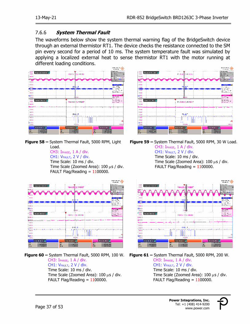
System Thermal Fault The waveforms below show the system thermal warning flag of the BridgeSwitch device through an external thermistor RT1. The device checks the resistance connected to the SM pin every second for a period of 10 ms. The system temperature fault was simulated by applying a localized external heat to sense thermistor RT1 with the motor running at different loading conditions.
Figure 58 – System Thermal Fault, 5000 RPM, Light
Load. CH3: IPHASE, 1 A / div. CH1: VFAULT, 2 V / div. Time Scale: 10 ms / div. Time Scale (Zoomed Area): 100 s / div. FAULT Flag/Reading = 1100000.
Figure 59 – System Thermal Fault, 5000 RPM, 30 W Load. CH3: IPHASE, 1 A / div. CH1: VFAULT, 2 V / div. Time Scale: 10 ms / div. Time Scale (Zoomed Area): 100 s / div. FAULT Flag/Reading = 1100000.
Figure 60 – System Thermal Fault, 5000 RPM, 100 W.
CH3: IPHASE, 1 A / div. CH1: VFAULT, 2 V / div. Time Scale: 10 ms / div. Time Scale (Zoomed Area): 100 s / div. FAULT Flag/Reading = 1100000.
Figure 61 – System Thermal Fault, 5000 RPM, 200 W. CH3: IPHASE, 1 A / div. CH1: VFAULT, 2 V / div. Time Scale: 10 ms / div. Time Scale (Zoomed Area): 100 s / div. FAULT Flag/Reading = 1100000.
RDR-852 BridgeSwitch BRD1263C 3-Phase Inverter 13-May-21
Page 38 of 53
Power Integrations, Inc. Tel: +1 (408) 414-9200 www.power.com
Abnormal Motor Operation Test This paragraph provides results during abnormal operation tests for appliances with motors as described in IEC 60335-1 (Safety of household and similar electrical appliances). The test includes:
Operation under stalled motor conditions Operation with one motor winding disconnected Running overload test
The test results demonstrate the integrated protection features of the BridgeSwitch under such abnormal conditions.
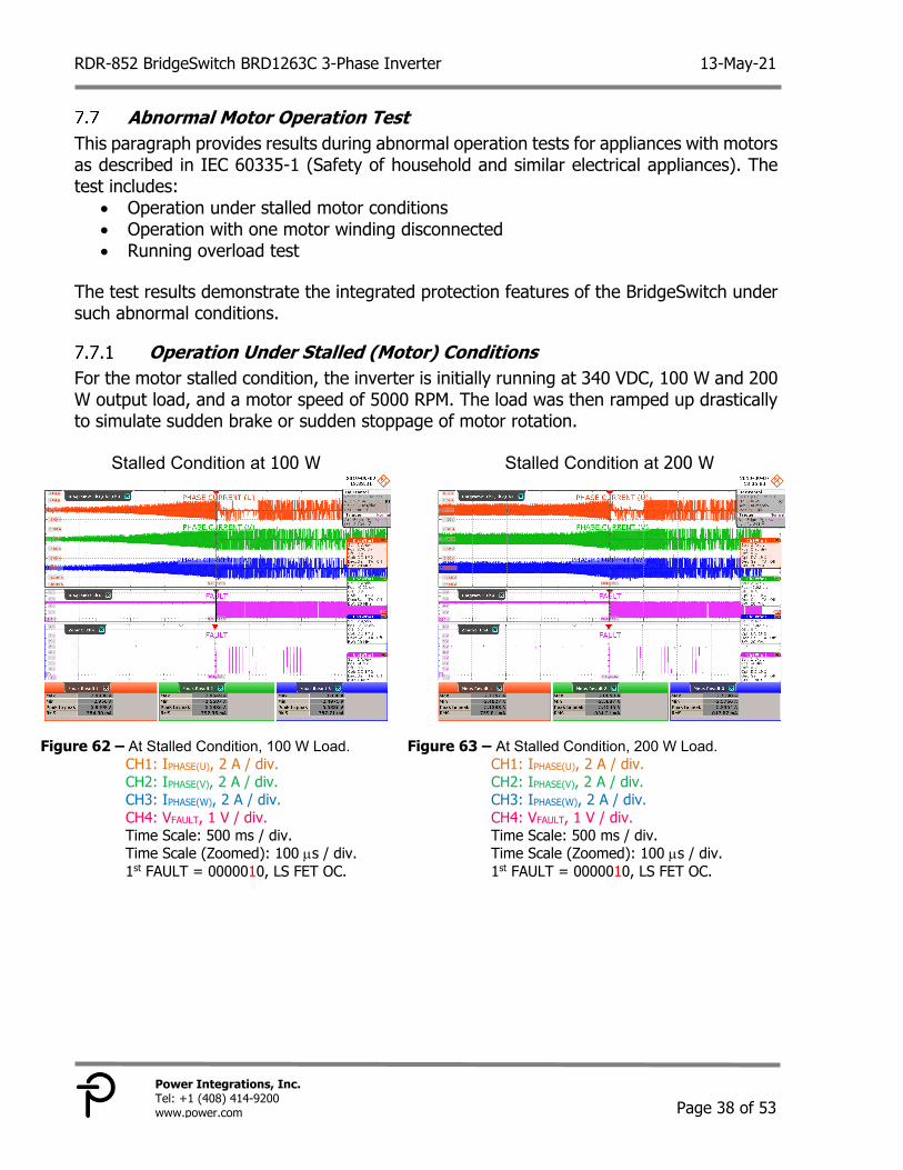
Operation Under Stalled (Motor) Conditions For the motor stalled condition, the inverter is initially running at 340 VDC, 100 W and 200 W output load, and a motor speed of 5000 RPM. The load was then ramped up drastically to simulate sudden brake or sudden stoppage of motor rotation.
Stalled Condition at 100 W Stalled Condition at 200 W
Figure 62 – At Stalled Condition, 100 W Load.
CH1: IPHASE(U), 2 A / div. CH2: IPHASE(V), 2 A / div. CH3: IPHASE(W), 2 A / div. CH4: VFAULT, 1 V / div. Time Scale: 500 ms / div. Time Scale (Zoomed): 100 s / div. 1st FAULT = 0000010, LS FET OC.
Figure 63 – At Stalled Condition, 200 W Load. CH1: IPHASE(U), 2 A / div. CH2: IPHASE(V), 2 A / div. CH3: IPHASE(W), 2 A / div. CH4: VFAULT, 1 V / div. Time Scale: 500 ms / div. Time Scale (Zoomed): 100 s / div. 1st FAULT = 0000010, LS FET OC.
13-May-21 RDR-852 BridgeSwitch BRD1263C 3-Phase Inverter
Page 39 of 53
Power Integrations, Inc. Tel: +1 (408) 414-9200
www.power.com
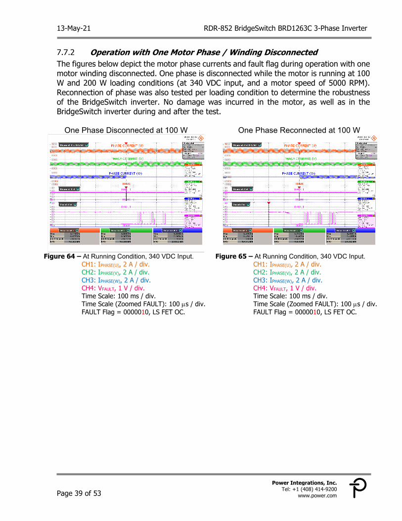
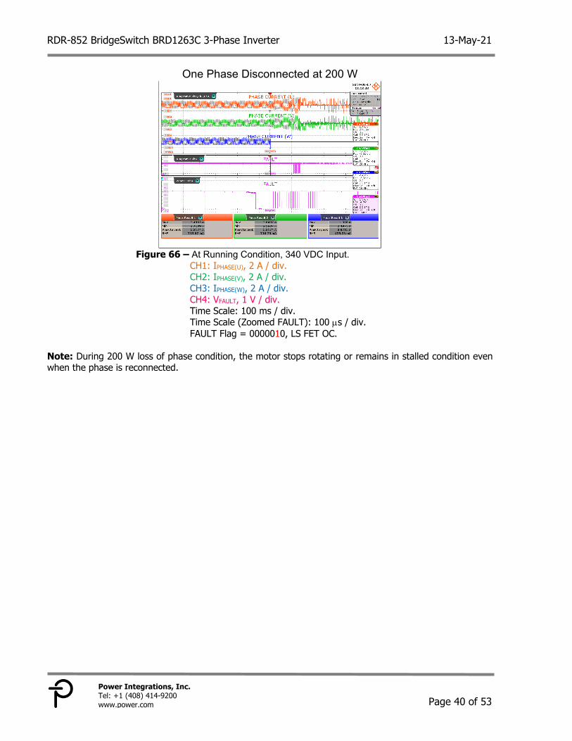
Operation with One Motor Phase / Winding Disconnected The figures below depict the motor phase currents and fault flag during operation with one motor winding disconnected. One phase is disconnected while the motor is running at 100 W and 200 W loading conditions (at 340 VDC input, and a motor speed of 5000 RPM). Reconnection of phase was also tested per loading condition to determine the robustness of the BridgeSwitch inverter. No damage was incurred in the motor, as well as in the BridgeSwitch inverter during and after the test.
One Phase Disconnected at 100 W One Phase Reconnected at 100 W
Figure 64 – At Running Condition, 340 VDC Input. CH1: IPHASE(U), 2 A / div. CH2: IPHASE(V), 2 A / div. CH3: IPHASE(W), 2 A / div. CH4: VFAULT, 1 V / div. Time Scale: 100 ms / div. Time Scale (Zoomed FAULT): 100 s / div. FAULT Flag = 0000010, LS FET OC.
Figure 65 – At Running Condition, 340 VDC Input. CH1: IPHASE(U), 2 A / div. CH2: IPHASE(V), 2 A / div. CH3: IPHASE(W), 2 A / div. CH4: VFAULT, 1 V / div. Time Scale: 100 ms / div. Time Scale (Zoomed FAULT): 100 s / div. FAULT Flag = 0000010, LS FET OC.
RDR-852 BridgeSwitch BRD1263C 3-Phase Inverter 13-May-21
Page 40 of 53
Power Integrations, Inc. Tel: +1 (408) 414-9200 www.power.com
One Phase Disconnected at 200 W
Figure 66 – At Running Condition, 340 VDC Input.
CH1: IPHASE(U), 2 A / div. CH2: IPHASE(V), 2 A / div. CH3: IPHASE(W), 2 A / div. CH4: VFAULT, 1 V / div. Time Scale: 100 ms / div. Time Scale (Zoomed FAULT): 100 s / div. FAULT Flag = 0000010, LS FET OC.
Note: During 200 W loss of phase condition, the motor stops rotating or remains in stalled condition even when the phase is reconnected.
13-May-21 RDR-852 BridgeSwitch BRD1263C 3-Phase Inverter
Page 41 of 53
Power Integrations, Inc. Tel: +1 (408) 414-9200
www.power.com
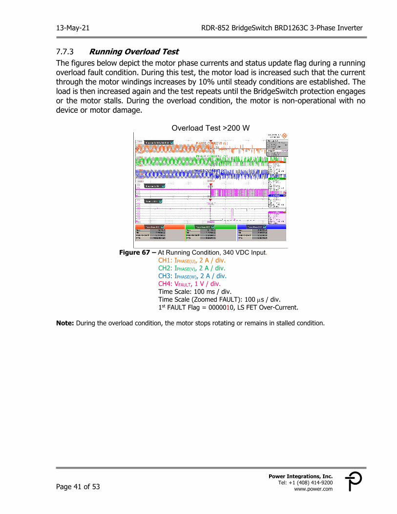
Running Overload Test The figures below depict the motor phase currents and status update flag during a running overload fault condition. During this test, the motor load is increased such that the current through the motor windings increases by 10% until steady conditions are established. The load is then increased again and the test repeats until the BridgeSwitch protection engages or the motor stalls. During the overload condition, the motor is non-operational with no device or motor damage.
Overload Test >200 W
Figure 67 – At Running Condition, 340 VDC Input. CH1: IPHASE(U), 2 A / div. CH2: IPHASE(V), 2 A / div. CH3: IPHASE(W), 2 A / div. CH4: VFAULT, 1 V / div. Time Scale: 100 ms / div. Time Scale (Zoomed FAULT): 100 s / div. 1st FAULT Flag = 0000010, LS FET Over-Current.
Note: During the overload condition, the motor stops rotating or remains in stalled condition.
RDR-852 BridgeSwitch BRD1263C 3-Phase Inverter 13-May-21
Page 42 of 53
Power Integrations, Inc. Tel: +1 (408) 414-9200 www.power.com
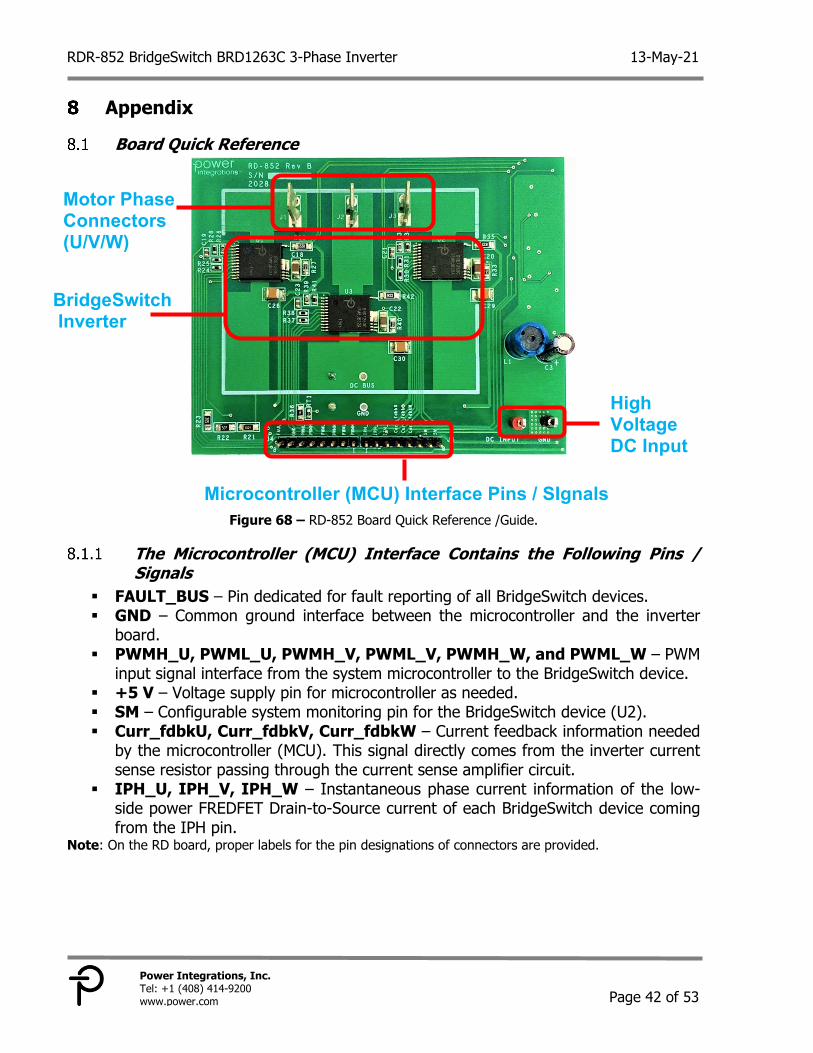
Appendix
Board Quick Reference
Figure 68 – RD-852 Board Quick Reference /Guide.
The Microcontroller (MCU) Interface Contains the Following Pins / Signals
FAULT_BUS – Pin dedicated for fault reporting of all BridgeSwitch devices. GND – Common ground interface between the microcontroller and the inverter
board. PWMH_U, PWML_U, PWMH_V, PWML_V, PWMH_W, and PWML_W – PWM
input signal interface from the system microcontroller to the BridgeSwitch device. +5 V – Voltage supply pin for microcontroller as needed. SM – Configurable system monitoring pin for the BridgeSwitch device (U2). Curr_fdbkU, Curr_fdbkV, Curr_fdbkW – Current feedback information needed
by the microcontroller (MCU). This signal directly comes from the inverter current sense resistor passing through the current sense amplifier circuit.
IPH_U, IPH_V, IPH_W – Instantaneous phase current information of the low-side power FREDFET Drain-to-Source current of each BridgeSwitch device coming from the IPH pin.
Note: On the RD board, proper labels for the pin designations of connectors are provided.
BridgeSwitch Inverter
Motor Phase Connectors (U/V/W)
High Voltage DC Input
Microcontroller (MCU) Interface Pins / SIgnals
13-May-21 RDR-852 BridgeSwitch BRD1263C 3-Phase Inverter
Page 43 of 53
Power Integrations, Inc. Tel: +1 (408) 414-9200
www.power.com
J4 Connector Pin Designation Pin No. Signal Type Comments
1 PWML_V Input Gate drive signal for low-side power FREDFET phase V. 2 PWMH_V Input Gate drive signal for high-side power FREDFET phase V. 3 PWML_W Input Gate drive signal for low-side power FREDFET phase W. 4 PWMH_W Input Gate drive signal for high-side power FREDFET phase W. 5 PWML_U Input Gate drive signal for low-side power FREDFET phase U. 6 PWMH_U Input Gate drive signal for high-side power FREDFET phase U. 7 GND n/a Ground reference for connector input and output signals. 8 FAULT_BUS Input/Output Single wire, bi-directional fault communication bus.
J5 Connector Pin Designation Pin No. Signal Type Comments
1 IPH_U Output Voltage signal proportional to the instantaneous phase low-side FREDFET Drain current of Phase U.
2 IPH_V Output Voltage signal proportional to the instantaneous phase low-side FREDFET Drain current of Phase V.
3 IPH_W Output Voltage signal proportional to the instantaneous phase low-side FREDFET Drain current of Phase W.
4 Curr_fdbkU Output Current feedback information needed by the microcontroller for phase U.
5 Curr_fdbkV Output Current feedback information needed by the microcontroller for phase V.
6 Curr_fdbkW Output Current feedback information needed by the microcontroller for phase W.
7 SM_W Input External input for system sensing (i.e. can be connected to an external thermistor for system temperature monitor via status communication bus)
8 +5 V Output Voltage supply pin for the microcontroller as needed Note: On the RD board, proper labels for the pin designations of connectors are provided.
RDR-852 BridgeSwitch BRD1263C 3-Phase Inverter 13-May-21
Page 44 of 53
Power Integrations, Inc. Tel: +1 (408) 414-9200 www.power.com
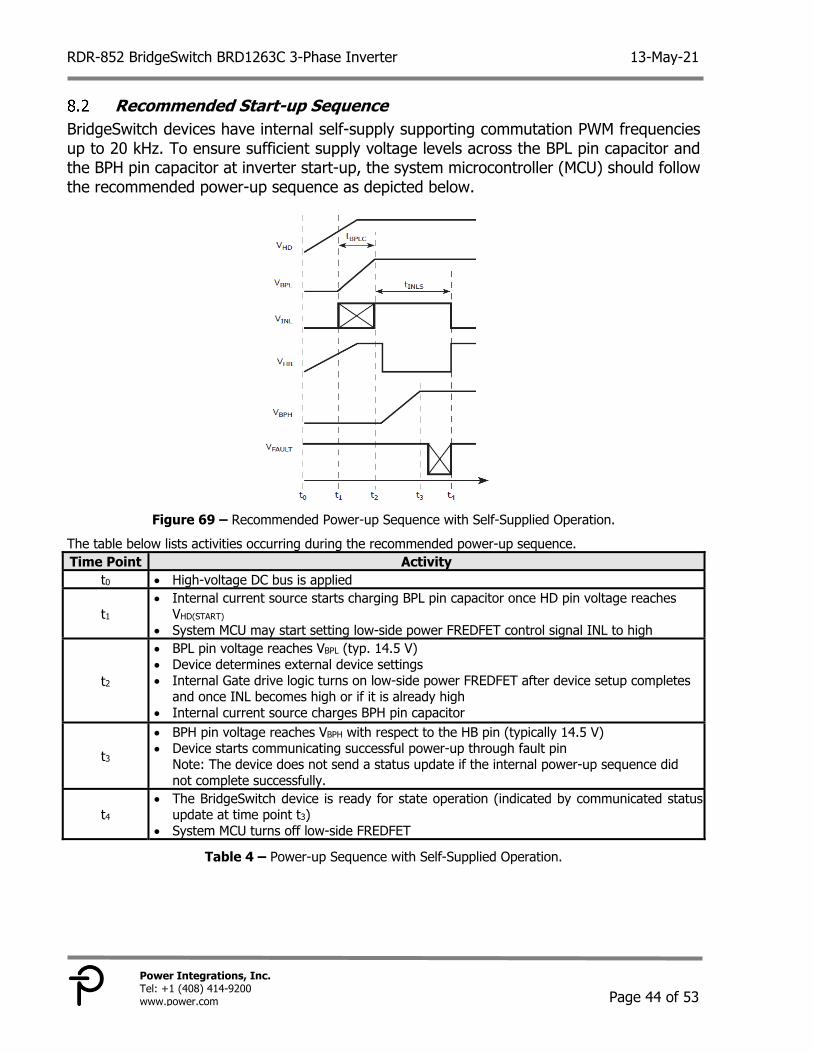
Recommended Start-up Sequence BridgeSwitch devices have internal self-supply supporting commutation PWM frequencies up to 20 kHz. To ensure sufficient supply voltage levels across the BPL pin capacitor and the BPH pin capacitor at inverter start-up, the system microcontroller (MCU) should follow the recommended power-up sequence as depicted below.
Figure 69 – Recommended Power-up Sequence with Self-Supplied Operation.
The table below lists activities occurring during the recommended power-up sequence. Time Point Activity
t0 High-voltage DC bus is applied
t1 Internal current source starts charging BPL pin capacitor once HD pin voltage reaches
VHD(START) System MCU may start setting low-side power FREDFET control signal INL to high
t2
BPL pin voltage reaches VBPL (typ. 14.5 V) Device determines external device settings Internal Gate drive logic turns on low-side power FREDFET after device setup completes
and once INL becomes high or if it is already high Internal current source charges BPH pin capacitor
t3 BPH pin voltage reaches VBPH with respect to the HB pin (typically 14.5 V) Device starts communicating successful power-up through fault pin
Note: The device does not send a status update if the internal power-up sequence did not complete successfully.
t4 The BridgeSwitch device is ready for state operation (indicated by communicated status
update at time point t3) System MCU turns off low-side FREDFET
Table 4 – Power-up Sequence with Self-Supplied Operation.
13-May-21 RDR-852 BridgeSwitch BRD1263C 3-Phase Inverter
Page 45 of 53
Power Integrations, Inc. Tel: +1 (408) 414-9200
www.power.com
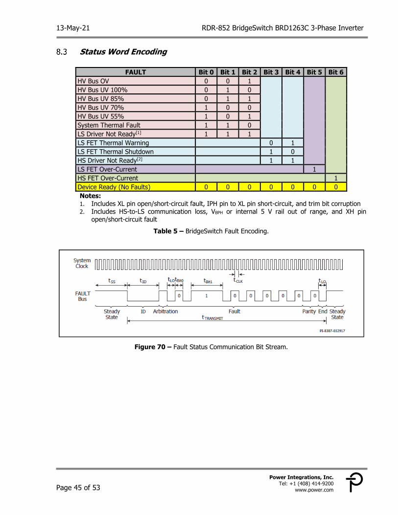
Status Word Encoding
FAULT Bit 0 Bit 1 Bit 2 Bit 3 Bit 4 Bit 5 Bit 6 HV Bus OV 0 0 1
HV Bus UV 100% 0 1 0 HV Bus UV 85% 0 1 1 HV Bus UV 70% 1 0 0 HV Bus UV 55% 1 0 1 System Thermal Fault 1 1 0 LS Driver Not Ready[1] 1 1 1 LS FET Thermal Warning 0 1 LS FET Thermal Shutdown 1 0 HS Driver Not Ready[2] 1 1 LS FET Over-Current 1 HS FET Over-Current 1 Device Ready (No Faults) 0 0 0 0 0 0 0 Notes: 1. Includes XL pin open/short-circuit fault, IPH pin to XL pin short-circuit, and trim bit corruption 2. Includes HS-to-LS communication loss, VBPH or internal 5 V rail out of range, and XH pin
open/short-circuit fault Table 5 – BridgeSwitch Fault Encoding.
Figure 70 – Fault Status Communication Bit Stream.
RDR-852 BridgeSwitch BRD1263C 3-Phase Inverter 13-May-21
Page 46 of 53
Power Integrations, Inc. Tel: +1 (408) 414-9200 www.power.com
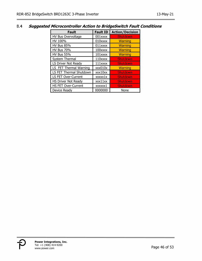
Suggested Microcontroller Action to BridgeSwitch Fault Conditions Fault Fault ID Action/Decision
HV Bus Overvoltage 001xxxx Shutdown HV 100% 010xxxx Warning HV Bus 85% 011xxxx Warning HV Bus 70% 100xxxx Warning HV Bus 55% 101xxxx Warning System Thermal 110xxxx Shutdown LS Driver Not Ready 111xxxx Shutdown LS FET Thermal Warning xxx010x Warning LS FET Thermal Shutdown xxx10xx Shutdown LS FET Over-Current xxxxx1x Shutdown HS Driver Not Ready xxx11xx Shutdown HS FET Over-Current xxxxxx1 Shutdown Device Ready 0000000 None
13-May-21 RDR-852 BridgeSwitch BRD1263C 3-Phase Inverter
Page 47 of 53
Power Integrations, Inc. Tel: +1 (408) 414-9200
www.power.com
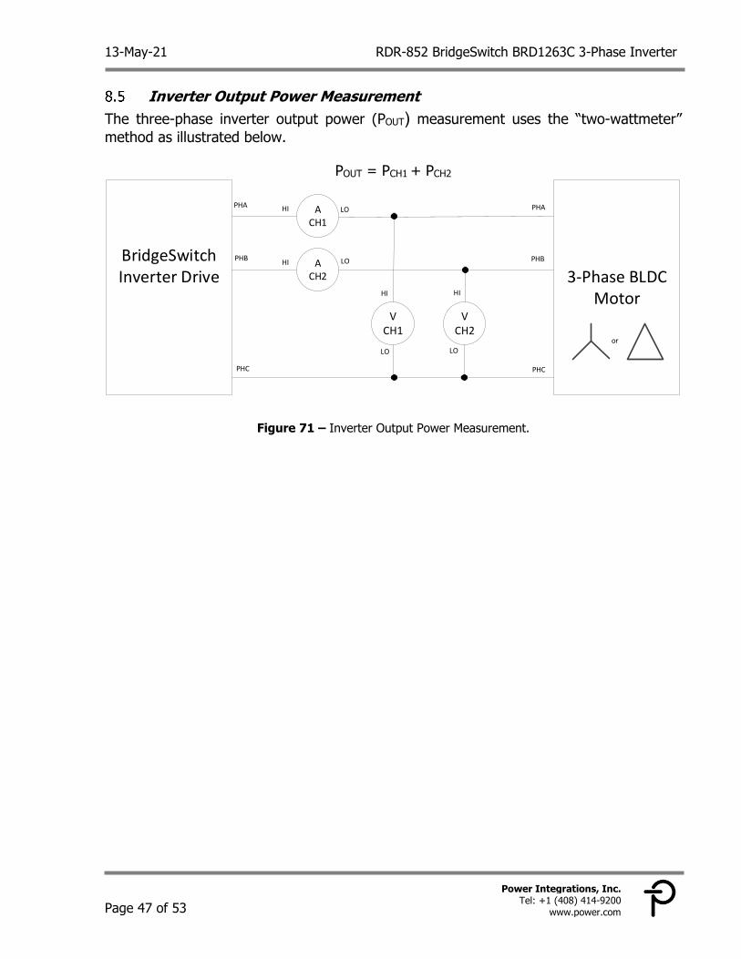
Inverter Output Power Measurement The three-phase inverter output power (POUT) measurement uses the “two-wattmeter” method as illustrated below.
POUT = PCH1 + PCH2
Figure 71 – Inverter Output Power Measurement.
BridgeSwitch Inverter Drive 3‐Phase BLDC
Motor
ACH1
ACH2
VCH1
VCH2
PHA
PHB
PHC PHC
PHB
PHA
or
HI
HI
HI HI
LO LO
LO
LO
RDR-852 BridgeSwitch BRD1263C 3-Phase Inverter 13-May-21
Page 48 of 53
Power Integrations, Inc. Tel: +1 (408) 414-9200 www.power.com
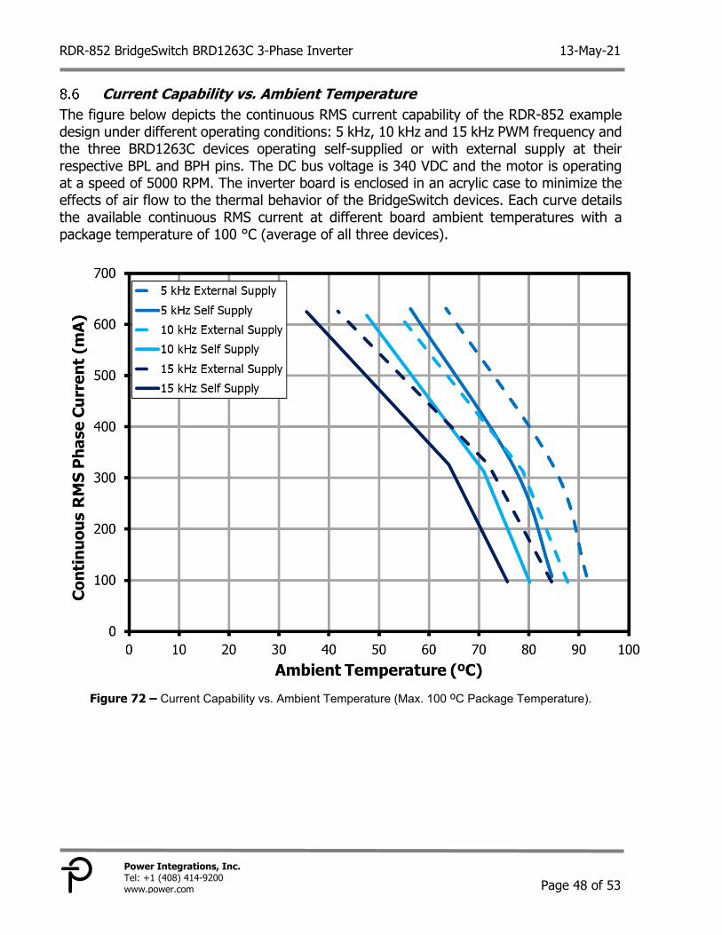
Current Capability vs. Ambient Temperature The figure below depicts the continuous RMS current capability of the RDR-852 example design under different operating conditions: 5 kHz, 10 kHz and 15 kHz PWM frequency and the three BRD1263C devices operating self-supplied or with external supply at their respective BPL and BPH pins. The DC bus voltage is 340 VDC and the motor is operating at a speed of 5000 RPM. The inverter board is enclosed in an acrylic case to minimize the effects of air flow to the thermal behavior of the BridgeSwitch devices. Each curve details the available continuous RMS current at different board ambient temperatures with a package temperature of 100 °C (average of all three devices).
Figure 72 – Current Capability vs. Ambient Temperature (Max. 100 ºC Package Temperature).
13-May-21 RDR-852 BridgeSwitch BRD1263C 3-Phase Inverter
Page 49 of 53
Power Integrations, Inc. Tel: +1 (408) 414-9200
www.power.com
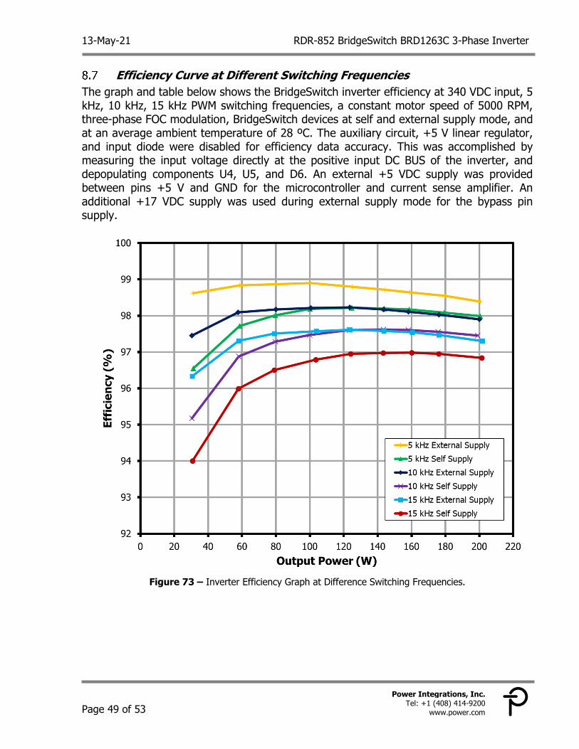
Efficiency Curve at Different Switching Frequencies The graph and table below shows the BridgeSwitch inverter efficiency at 340 VDC input, 5 kHz, 10 kHz, 15 kHz PWM switching frequencies, a constant motor speed of 5000 RPM, three-phase FOC modulation, BridgeSwitch devices at self and external supply mode, and at an average ambient temperature of 28 ºC. The auxiliary circuit, +5 V linear regulator, and input diode were disabled for efficiency data accuracy. This was accomplished by measuring the input voltage directly at the positive input DC BUS of the inverter, and depopulating components U4, U5, and D6. An external +5 VDC supply was provided between pins +5 V and GND for the microcontroller and current sense amplifier. An additional +17 VDC supply was used during external supply mode for the bypass pin supply.
Figure 73 – Inverter Efficiency Graph at Difference Switching Frequencies.
RDR-852 BridgeSwitch BRD1263C 3-Phase Inverter 13-May-21
Page 50 of 53
Power Integrations, Inc. Tel: +1 (408) 414-9200 www.power.com
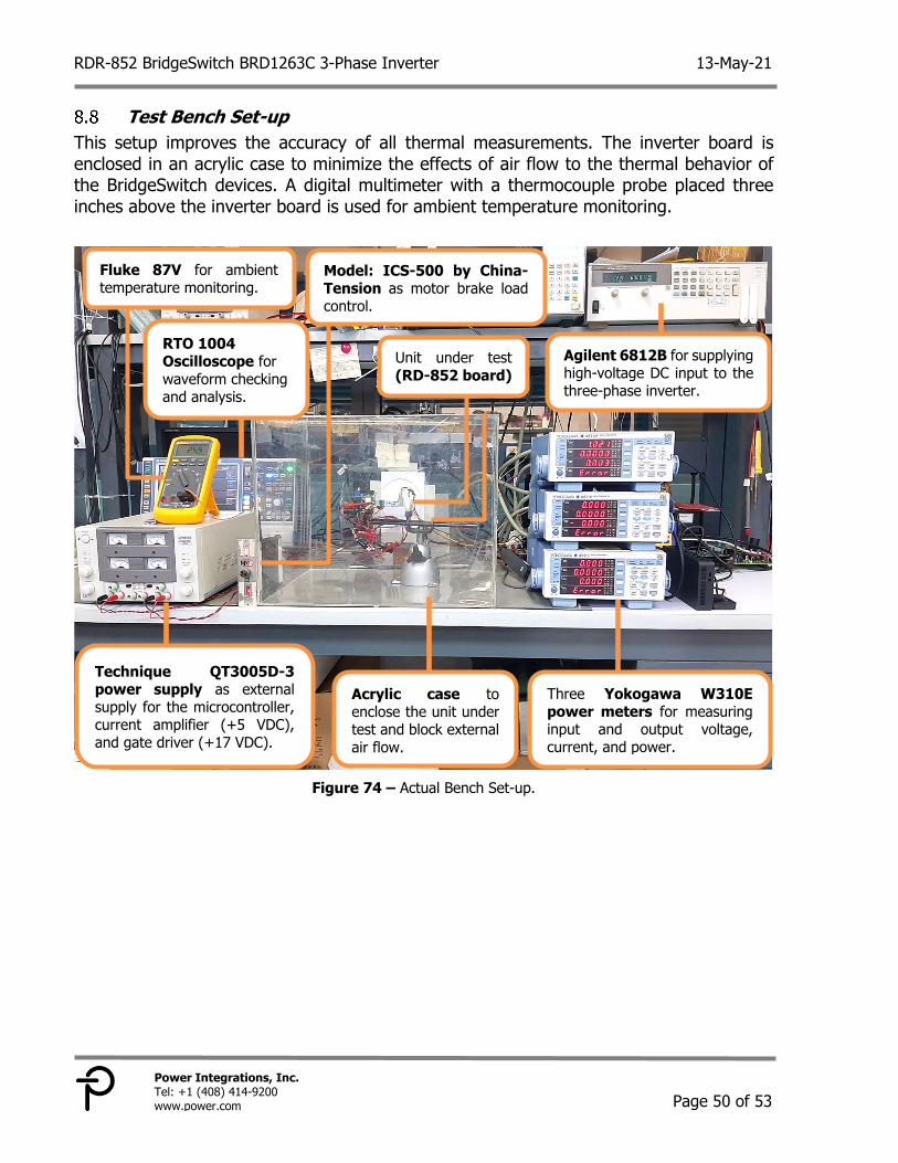
Test Bench Set-up This setup improves the accuracy of all thermal measurements. The inverter board is enclosed in an acrylic case to minimize the effects of air flow to the thermal behavior of the BridgeSwitch devices. A digital multimeter with a thermocouple probe placed three inches above the inverter board is used for ambient temperature monitoring.
Figure 74 – Actual Bench Set-up.
Fluke 87V for ambient temperature monitoring.
Technique QT3005D-3 power supply as external supply for the microcontroller, current amplifier (+5 VDC), and gate driver (+17 VDC).
Model: ICS-500 by China-Tension as motor brake load control.
Acrylic case to enclose the unit under test and block external air flow.
Unit under test (RD-852 board)
Agilent 6812B for supplying high-voltage DC input to the three-phase inverter.
Three Yokogawa W310E power meters for measuring input and output voltage, current, and power.
RTO 1004 Oscilloscope for waveform checking and analysis.
13-May-21 RDR-852 BridgeSwitch BRD1263C 3-Phase Inverter
Page 51 of 53
Power Integrations, Inc. Tel: +1 (408) 414-9200
www.power.com
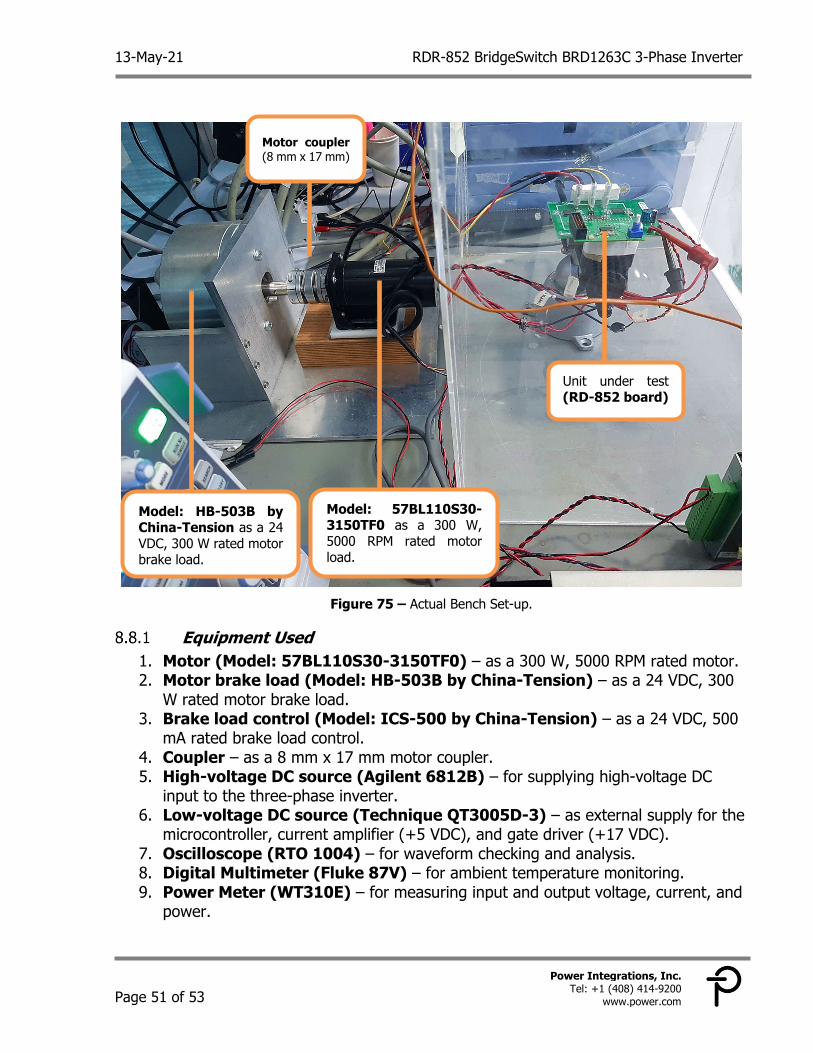
Figure 75 – Actual Bench Set-up.
Equipment Used 1. Motor (Model: 57BL110S30-3150TF0) – as a 300 W, 5000 RPM rated motor. 2. Motor brake load (Model: HB-503B by China-Tension) – as a 24 VDC, 300
W rated motor brake load. 3. Brake load control (Model: ICS-500 by China-Tension) – as a 24 VDC, 500
mA rated brake load control. 4. Coupler – as a 8 mm x 17 mm motor coupler. 5. High-voltage DC source (Agilent 6812B) – for supplying high-voltage DC
input to the three-phase inverter. 6. Low-voltage DC source (Technique QT3005D-3) – as external supply for the
microcontroller, current amplifier (+5 VDC), and gate driver (+17 VDC). 7. Oscilloscope (RTO 1004) – for waveform checking and analysis. 8. Digital Multimeter (Fluke 87V) – for ambient temperature monitoring. 9. Power Meter (WT310E) – for measuring input and output voltage, current, and
power.
Model: HB-503B by China-Tension as a 24 VDC, 300 W rated motor brake load.
Model: 57BL110S30-3150TF0 as a 300 W, 5000 RPM rated motor load.
Unit under test (RD-852 board)
Motor coupler (8 mm x 17 mm)

RDR-852 BridgeSwitch BRD1263C 3-Phase Inverter 13-May-21
Page 52 of 53
Power Integrations, Inc. Tel: +1 (408) 414-9200 www.power.com
Revision History Date Author Rev. Description & Changes Approval
04-Feb-20 MQC 1.0 Initial Release. Apps & Mktg 27-Jul-20 SM 1.1 Schematic, PCB, and Various Updates. Apps & Mktg 12-Aug-20 KM 1.2 Added Alternate J4, J5 Supplier. Apps & Mktg
13-May-21 SM 1.3 Thermals and Efficiency Updates – Closed Case Setup. Apps & Mktg

13-May-21 RDR-852 BridgeSwitch BRD1263C 3-Phase Inverter
Page 53 of 53
Power Integrations, Inc. Tel: +1 (408) 414-9200
www.power.com
For the latest updates, visit our website: www.power.com Reference Designs are technical proposals concerning how to use Power Integrations’ gate drivers in particular applications and/or with certain power modules. These proposals are “as is” and are not subject to any qualification process. The suitability, implementation and qualification are the sole responsibility of the end user. The statements, technical information and recommendations contained herein are believed to be accurate as of the date hereof. All parameters, numbers, values and other technical data included in the technical information were calculated and determined to our best knowledge in accordance with the relevant technical norms (if any). They may base on assumptions or operational conditions that do not necessarily apply in general. We exclude any representation or warranty, express or implied, in relation to the accuracy or completeness of the statements, technical information and recommendations contained herein. No responsibility is accepted for the accuracy or sufficiency of any of the statements, technical information, recommendations or opinions communicated and any liability for any direct, indirect or consequential loss or damage suffered by any person arising therefrom is expressly disclaimed. Power Integrations reserves the right to make changes to its products at any time to improve reliability or manufacturability. Power Integrations does not assume any liability arising from the use of any device or circuit described herein. POWER INTEGRATIONS MAKES NO WARRANTY HEREIN AND SPECIFICALLY DISCLAIMS ALL WARRANTIES INCLUDING, WITHOUT LIMITATION, THE IMPLIED WARRANTIES OF MERCHANTABILITY, FITNESS FOR A PARTICULAR PURPOSE, AND NON-INFRINGEMENT OF THIRD PARTY RIGHTS. Patent Information The products and applications illustrated herein (including transformer construction and circuits’ external to the products) may be covered by one or more U.S. and foreign patents, or potentially by pending U.S. and foreign patent applications assigned to Power Integrations. A complete list of Power Integrations’ patents may be found at www.power.com. Power Integrations grants its customers a license under certain patent rights as set forth at http://www.power.com/ip.htm. Power Integrations, the Power Integrations logo, CAPZero, ChiPhy, CHY, DPA-Switch, EcoSmart, E-Shield, eSIP, eSOP, HiperPLC, HiperPFS, HiperTFS, InnoSwitch, Innovation in Power Conversion, InSOP, LinkSwitch, LinkZero, LYTSwitch, SENZero, TinySwitch, TOPSwitch, PI, PI Expert, PowiGaN, SCALE, SCALE-1, SCALE-2, SCALE-3 and SCALE-iDriver, are trademarks of Power Integrations, Inc. Other trademarks are property of their respective companies. ©2019, Power Integrations, Inc. Power Integrations Worldwide Sales Support Locations
WORLD HEADQUARTERS 5245 Hellyer Avenue San Jose, CA 95138, USA. Main: +1-408-414-9200 Customer Service: Worldwide: +1-65-635-64480 Americas: +1-408-414-9621 e-mail: [email protected] CHINA (SHANGHAI) Rm 2410, Charity Plaza, No. 88, North Caoxi Road, Shanghai, PRC 200030 Phone: +86-21-6354-6323 e-mail: [email protected] CHINA (SHENZHEN) 17/F, Hivac Building, No. 2, Keji Nan 8th Road, Nanshan District, Shenzhen, China, 518057 Phone: +86-755-8672-8689 e-mail: [email protected]
GERMANY (AC-DC/LED Sales) Einsteinring 24 85609 Dornach/Aschheim Germany Tel: +49-89-5527-39100 e-mail: [email protected] GERMANY (Gate Driver Sales) HellwegForum 1 59469 Ense Germany Tel: +49-2938-64-39990 e-mail: igbt-driver.sales@ power.com INDIA #1, 14th Main Road Vasanthanagar Bangalore-560052 India Phone: +91-80-4113-8020 e-mail: [email protected]
ITALY Via Milanese 20, 3rd. Fl. 20099 Sesto San Giovanni (MI) Italy Phone: +39-024-550-8701 e-mail: [email protected] JAPAN Yusen Shin-Yokohama 1-chome Bldg. 1-7-9, Shin-Yokohama, Kohoku-ku Yokohama-shi, Kanagawa 222-0033 Japan Phone: +81-45-471-1021 e-mail: [email protected] KOREA RM 602, 6FL Korea City Air Terminal B/D, 159-6 Samsung-Dong, Kangnam-Gu, Seoul, 135-728 Korea Phone: +82-2-2016-6610 e-mail: [email protected]
SINGAPORE 51 Newton Road, #19-01/05 Goldhill Plaza Singapore, 308900 Phone: +65-6358-2160 e-mail: [email protected] TAIWAN 5F, No. 318, Nei Hu Rd., Sec. 1 Nei Hu District Taipei 11493, Taiwan R.O.C. Phone: +886-2-2659-4570 e-mail: [email protected] UK Building 5, Suite 21 The Westbrook Centre Milton Road Cambridge CB4 1YG Phone: +44 (0) 7823-557484 e-mail: [email protected]