reliability issues of flash memory cells - proceedings of ... · reliability issues of flash memory...
TRANSCRIPT

Reliability Issues of Flash Memory Cells ~
SEIICHI ARITOME, RIICHIRO SHIROTA, GERTJAN HEMINK, TETSUO ENDOH, AND FUJI0 MASUOKA
Invited Paper
The reliability issues of Flash electrically erasable pro- grammable read-only memory (Flash EEPROM) are reviewed in this paper. The reduction of the memory cell size and improvement in the reliability have been realized by several breakthroughs in the device technology; in particular, the reliability of the ETOX and NAND structure EEPROM will be discussed in detail. Flash EEPROM is expected to be a very promising device fo r a large nonvolatile memory market. One of the most promising applications is the replacement of the conventional magnetic hard disk by nonvolatile memories.
I. INTRODUCTION Recent progress in computers requires further efforts in
developing higher density and higher reliability nonvolatile semiconductor memories. A breakthrough in the field of nonvolatile memories was the invention of the Flash EEP- ROM [ l ] . The Flash EEPROM has many advantages in comparison with other nonvolatile memories. Therefore, the Flash EEPROM explosively accelerated the development of higher density EEPROM’s. This paper describes the technical trends and reliability issues of Flash EEPROM’s.
In the following section, the trends in Flash EEPROM development will be reviewed. After that, the reliability of several types of Flash memories will be discussed. And finally, the reliability of thin oxide and interpoly dielectrics are discussed.
11. HISTORY OF THE FLASH EEPROM Table 1 shows the history of Flash EEPROM develop-
ment. The first modem Flash EEPROM was proposed at the 1984 IEDM by Masuoka et al. [ I ] . Fig. 1 shows the cell structure of this first Flash EEPROM. The Flash EEPROM is realized in a three-layer polysilicon technology. The first polysilicon is used as the erase gate, the second polysilicon as the floating gate, and the third polysilicon is used as the control gate. Programming can be performed by hot electron injection from the channel, similar to that of
Manuscript received October 22, 1992; revised November 19. 1992. The authors are with the ULSI Research Center, Toshiba Corporation,
IEEE Log Number 9209252. I Komukai-Toshiba-cho, Saiwai-ku, Kawasaki 210, Japan.
COntrQl Gate
Erase Gate t poly S i )
E:: q( VS
Fig. 1. Top and cross-sectional view of the Flash EEPROM cell [ [ I .
the ultraviolet erasure-type EPROM (UV-EPROM). The erasure is carried out by extracting the electrons from the floating gate to the erase gate for all bits at the same time. This EEPROM structure was called a Flash EEPROM because the complete memory array could be erased very quickly. At present, the name Flash EEPROM is used for all EEPROM’s in which all or a large number of cells, called a block or a page, are erased at the same time.
The Flash EEPROM has several advantages in com- parison with UV-EPROM. The erasing time is less than 1 s, while the erase time for an UV-EPROM is about 10 min. Moreover, the UV-EPROM needs an expensive package because of the UV transparent quartz window, and the UV-EPROM has to be taken out of the system for the erase. Thus, some companies have stopped developing UV-EPROM in favor of the development of the Flash EEPROM.
For erasure, the conventional EEPROM can achieve selective erase of each byte, while the Flash EEPROM erases all bits at the same time. This is a disadvantage of the Flash EEPROM in comparison with the conventional EEPROM. However, the cell size of the Flash EEPROM is less than that of the conventional EEPROM, and is even comparable with EPROM and DRAM. Therefore, the cost per bit is greatly reduced. Now, the market of the Flash
001 8-92 19/93$03.00 0 1993 IEEE
776 PROCEEDINGS OF THE IEEE. VOL. 81. NO. 5 . MAY 1993

Table 1 History of Flash Memory
1978
1984
1985
I985
I987
1987
1987
1988
1988
1988
1988
1988
I988
I988
I989
1989
I989
1989
1989
I989
1989
I990
I990
I990
1990
1990
I990
1990
1990
1991
1991
1991
1991
1991
EAROM
Flash memory
Flash memory (256 kb)
Source-erase type Flash
Drain-erase type Flash ( 128 kb)
NAND structure EEPROM
Source-erase type Flash
ETOX-type Flash (256 kb)
NAND EEPROM
ETOX-type Flash
ETOX-type Flash, reliability
NAND EEPROM
Poly-poly erase Flash
Contactless Flash
Contactless Flash (256 kb)
Gate-negative erase
NAND EEPROM (4 Mb)
ETOX-type Flash ( I Mb)
Sidewall Flajh
Contactless Flash
Punchthrough erase
Well-erase
NAND EEPROM
Contactless Flash, ACEE
NAND EEPROM, well erase
FACE cell
Gate-negative erase
Contactlesv Flash
Bipolarity Write/Erase
PB-FACE cell
Bunt-pulse erase
Sector-erase
Flash cell, scaling
Self-conversion erase
D. C. Guterman et al. 1371
F. Masuoka et al. [ I ]
F. Masuoka er al. 121, 131
S. Mukherjee et U/. [4]
G. Samachisa et al. [SI, [6]
F. Masuoka er al. 171
H. Kume er al. 181
V. N. Kynett rt al.191, I l0J
R. Shirota et al. [ I I ]
S. Tam er al. 1121
G. Verma er al. [ 131
M. Momodomi et al. [ 141
R. Karerounian er al. [ 151
M. Gill et U / . [ 161
S. D’Arrigo et u/.[17]
S. Haddad et al. [ 181
M. Momodomi er N I . [ 191
V. N. Kynett et al. [20]
K. Naruke er d. [21 I
M. Gill et al. [22]
T. Endoh er d. [23]
S. Aritome et U / . 1241
Y. lwata Flash 1251
B. Riemenschneider et N I . 1261
R. Kirisawa et al. [271
B. J. Woo e / d. (281
N. Ajika e/ U / . (291
M . Gill et d. [30]
S. Aritome et d. 13 I ]
B. J . Woo er d. [32]
N. Kodama et al. (331
H. Kume er d. 1341
K. Yoshikawa et a/. 1351
S. Yamada et d . [36]
TI
Toshiba
Toyhiba
EXCEL
Seeq, UCB
Toshiba
Hitachi
INTEL
Toshiba
INTEL
INTEL
Toshiba
WSI
TI
TI
AMD
Toshiba
INTEL
Toshiba
TI
Toshiba
Toshiba
Toshiba
TI
Toshiba
INTEL
Mitsubishi
TI
Toshiba
INTEL
NEC
Hitachi
Toshiba
Toshiba
EEPROM is as large as that of the conventional EEPROM, and will grow up.
Because of these advantages, the Flash EEPROM has been actively developed in many LSI companies, as shown
in Table 1. In 1985, Mukherjee et al. proposed a source-erase type
Flash memory cell [4], called the ETOX (EPROM with tunnel oxide) cell. The structure of this cell is the same
ARITOME et U/ . : RELIABILITY ISSUES OF FLASH MEMORY CELLS 777

Flootifq ate E r a Gate Tumel Oxide Euoand mly-si) (First Poly-Si)
Fig. 2. Three kinds of Flash EEPROM cells.
Memory Transistori
8 7 I b i t
6
5 4 3 2 I
as that of the UV-EPROM. The cell is programmed to a high threshold state by means of channel hot electron injection, with the control gate and the drain connected to a high voltage. Erasing the cell to a low threshold state is performed by Fowler-Nordheim tunneling of electrons from the floating gate to the source diffusion layer by grounding the control gate and applying a high voltage
\id - n+--pRn;t
SOURCE DRAIN
v a q - r -
n+--pRn;t SOURCE DRAIN
SUBSTRATE
Fig. 4. by CHE injection.
Schematic description of Flash EEPROM programming
-4 -1 to the source diffusion. Erasure can be achieved with less than 15 V on the source diffusion layer. Since 1985,
Fig. 5. ~ ;,, distribution in programmed and erased State
the performance of this ETOX flash memory cell has been improved [Fig. 2(b)] by several companies; as a result. 8 Mb flash memories can be fabricated at this 111. RELIABILITY OF THE ETOX FLASHEEPROM
moment. At the 1987 I S S C ~ , Samachisa al. 151 proposed a
drain-erase type Flash EEPROM cell with two levels of polysilicon, as shown in Fig. 2 ( ~ ) . The cell can thought of as two transistors in series. One is a floating-gate memory transistor, similar to an EPROM cell. The other one is a simple enhancement transistor controlled by the control gate. This series enhancement transistor is used as a select transistor. The cell is programmed by hot electron injection and erased by electron tunneling between the floating gate and drain.
was proposed by
In this section, the cell operation and the reliability of the ETOX-type flash cell will be discussed. First, the operation of the cell will be discussed. After that, reliability-related issues, such as disturb, endurance, and retention, will be discussed.
A. cell Operation Programming of the cell is done in a similar way as
in traditional EPROM,s, by channel hot electron injection (CHE), as shown in Fig. 4. The cell is programmed to a high threshold state "0," as shown in Fig. 5 . A shallow drain junction and an optimized channel profile are used to In 19873 a NAND structured
Masuoka et t71. This structure reduces the size enhance CHE injection. Electrical is accomplished without Of the device The NAND by Fowler-Nordheim tunneling of electrons from the float-
ing gate to the source diffusion, as shown in Fig. 6. The cell is erased to a low threshold state. A graded source junction [81 permits the application of high
B. Disturb Mechanisms The two principal memory cell disturb mechanisms that
can occur during programming of an array are called gate- disturb (DC program) and drain-disturb (program disturb)
structure cell arranges a number of bits in series, as shown in Fig' 3' The has One 'Ontact area per 2 b. However, for a NAND structure cell, only one contact hole is required per two NAND structure cells. As a result, the NAND cell can realize a smaller cell area per bit than the current EPROM. Several improvements of the NAND structure cell make it possible to operate the cell with a single 5 V power supply and to use sector erase [ 1 11, [ 141, [191, 1241, [251, V71.
778 PROCEEDINGS OF THE IEEE, VOL. 81, NO. 5. MAY 1993

Vd (Open)
L n t SOURCE DRAIN
SUB
Fig. 6. Schematic description of Flash EEPROM electrical erase by Fowler-Nordheim tunneling of electrons from the floating gate to the source.
S : ( Source = 0 V )
Fig. 7. Schematic description of disturb during programming.
[13]. These mechanisms can occur in memory cells sharing a common word line (WL) or a common bit line (BL) while one of the cells is programmed. The effect of these disturbs on the different cells of the memory array is shown in Fig. 7.
Gate-disturb occurs in unprogrammed or erased cells which are connected to the same word line as the cell that is being programmed. These cells have a low cell threshold voltage. During the programming operation, the common word line is connected to a high voltage. The electric field across the tunnel oxide becomes high, and may cause tunneling of electrons to the floating gate from the substrate. The threshold voltage of the cell will increase, and in severe cases the cell is programmed unintentionally.
Drain-disturb occurs in programmed cells, which are on the same bit line as the cell that is being programmed. These cells will experience a high electric field between the floating gate and the drain. This may cause electrons to tunnel from the floating gate to drain, and lead to a reduced cell threshold voltage.
An important design consideration is a proper selection of the programming voltages to minimize these disturbs. The write/erase cycling of the cell also affects these disturbs. Verma et al. [I31 showed that the drain-disturb character- istics of the flash memory devices are excellent with no measurable change until several thousand cycles. However, write/erase cycling has an influence on the gate-disturb behavior. Fig. 8 shows the gate-disturb time as a function of cycling. Before cycling, the disturb time is about 100 s. After 100 cycles, this margin is decreased about two-three orders of magnitude. This degradation of the gate-disturb is caused by hole trapping during erasing, as will be shown in the following section [ 131.
L
4 0.10 In
0
C y c l e s
Fig. 8. Gate-disturb time as a function of cycling. - Fig. 9. Schematic cross-sectional view of the SISOS cell
C. Overerasing As shown in Fig. 5, the threshold voltage of a cell in the
programmed state is higher than 6.5 V. And the threshold voltage of a cell in the erased state is limited from 0.5 to 3.5 V. Electrical erase is not self-limiting. Therefore, elec- trical erase can leave the floating gate positively charged, thus turning the memory transistor into a depletion-mode transistor; this is called overerasing. The bit-line leakage current caused by this depletion-mode transistor may cause problems during the reading of the cells.
In order to solve this overerasing problem, several meth- ods were proposed [211, [91, 1201.
A series enhancement transistor can be used to prevent the leakage current, as has been shown in the previous section. Another similar method is to use the sidewall select-gate type cell. Naruke et al. proposed a Flash EEP- ROM cell which consists of a stacked-gate MOSFET with a sidewall select-gate on the source side (SISOS cell) [20], as shown in Fig. 9. The cell has a select-gate which prevents undesirable leakage current due to overerasing. This cell has some additional advantages. The cell is programmed by channel hot electron injection at the source side, and is erased by Fowler-Nordheim tunneling of electrons from the floating gate to the drain. The programming by source side injection makes i t possible to optimize the drain junction for erase by Fowler-Nordheim tunneling without having an influence on the generation of hot electrons.
The verified-erase method [20] is another means used to prevent overerase. An erase step is carried out by raising the source junction of all cells in the memory array to the erase voltage with all control gates grounded. Subsequently, a read operation is performed with a voltage of 3.2 V applied to the control gate. This 3.2 V is the upper limit for the threshold voltage of a cell in the erased state. If some
ARITOME er U / ' RELIABILITY ISSUES OF FLASH MEMORY Ck.LLS 719

’ ’ 10’ 102 103 104 I I I I I 1
Stress time Lmsecl
Fig. 10. Threshold voltage versus drain-stress time.
bits require more time to reach the erased state, erasing is performed again. The erase verify sequence is repeated until all cells in the array have a threshold voltage less than or equal to the 3.2 V maximum. It is shown in [20] that this verified erase method effectively suppresses overerasing.
A self-convergence erasing scheme, which is proposed by Yamada et al. [36], can also be used to prevent over- erasing. This method uses avalanche hot carrier injection after erasure by Fowler-Nordheim tunneling. The threshold voltages converge to a certain “steady state,” as shown in Fig. 10. The steady state is caused by a balance between avalanche hot electron injection and avalanche hot hole injection into the floating gate. A tight distribution of the threshold voltages and stable erasure without overerase can be accomplished in this way.
D. Write/Eruse Cycling Endurance Due to the presence of a high voltage at the gated-diode
junction during erasing, holes are inevitably generated by band-to-band tunneling [38], [39], and a small amount of them are injected into the oxide after being accelerated in the depletion region. Hot-hole injection during erasing has been reported to cause variations in the erased threshold voltages of the cells in the memory array [8], and trapped holes in the oxide were shown to degrade the charge retention of memory cells [ 131, [ 181.
In order to suppress the degradation of memory cells, several solutions have been proposed. The simplest method is to reduce the applied voltage to the source. Table 2 shows the data loss of a flash memory cell after various cycling conditions. The average charge loss is small in the case of a low applied voltage to the source because the hot-hole injection due to band-to-band tunneling is suppressed. The low electric field across the tunnel oxide during erasing also results in excellent write/erase endurance characteristics. Fig. I 1 shows the distribution versus write/erase cycles [20]. The plot shows that even after one million write/erase cycles, a program read margin of more than 2 V exists.
In order to realize both a high erase speed and an acceptable writelerase endurance, negative gate erasure has been proposed [ 181. Haddad et al. [ 181 compared the gate negative erase and the source erase method. Fig. 12 shows the gate-disturb after negative gate erasing and sources
Table 2 Charge Loss of ETOX Flash EEPROM Cell after 100 Cycles
Cycling Condition Average Charge Loss
EEPROM program (I b > 0 V) and erase (I, < 0 V)
EEPROM programElash erase 0.51 V at I&,,,,, = 12.5 V; I,, = 0 V
EEPROM programElash erase 0.33 V at I,,,,,, = 11.5 V; I,, - 1 . j V
0.1 V
EEPROM programElash erase 0.24 V at I;,,,,,, = 8.5 V; I:.q = -6 V
Uncycled 0.12 v
10.5
9
2 7.5
L I
t 1 PROGRAM READ MARGlN - 1 VCC MAX VCC MIN
ERASE READ MARGIN
ERASE VT MIN
1 10 100 1000 10000 100000 1M
NUMBER OF CYCLES Fig. 11. Endurance characteristics
erasing. No threshold voltage shift is observed for the cell erased under the gate negative erasing. This indicates that hot-hole injection is effectively suppressed by gate negative erasing. However, the gate-disturb after source erasing is significant. These data strongly support a model of hot- hole injection and hole trapping in the oxide during source erasing.
E. Datu Retention In floating-gate memories, the stored charge can leak
away from the floating gate through the gate oxide or through the interpoly dielectrics. This leakage, caused by mobile ions, oxide defects, or other mechanisms, results
780 PROCEEDINGS OF THE IEEE. VOL. 81. NO. 5. MAY 1993

+1 .o
h
> +0.6 Y
5 +0.2
-0.2 1 1 o-2 lo-’ loo 1 0’ 1 o2
Gate Disturb time ( sec )
Fig. 12. Threshold voltage shift during gate disturb.
in a shift of the threshold voltage of the memory cell. The threshold voltage shift can also be caused by the detrapping of electrons or holes from oxide traps.
Different charge loss mechanisms have been described in [46], [47]. These mechanism are briefly discussed below. The first mechanism is thermionic emission over the image force lowered potential barrier. However, this mechanism is not dominating since the barrier height for thermionic emission is considerably higher than the activation energies for the other charge loss mechanism. The second mecha- nism is called electron detrapping. The activation energy for this type of charge loss is about 1.4 eV. Because the intrinsic charge loss rate decreases with time and stops after a threshold voltage drop of about 0.5 V [47], this type of charge loss is associated with the detrapping of electrons that are trapped in the oxide. The third mechanism is related to defects in the oxide. This mechanism can result in both charge loss and gain, depending on the biasing condition. The activation energy for this kind of charge loss is about 0.6 eV [47]. The fourth mechanism is related to contamination. Positive ions entering the memory cell may compensate a part of the negative charge stored on the floating gate. The activation energy for charge loss by contamination is about 1.2 eV [47].
Kynett et al. showed the results of data retention tests for a 1 Mb Flash memory. Accelerated retention bake experiments done at 250°C for 168 h indicate that after lo4 write/erase cycles, flash memory will exhibit only a 0.7 V program Vth shift [20]. Furthermore, a retention bake of 52 h produced less than a 0.5 V Vtk, shift in programmed devices which have been through more than one million write/erase cycles. The program read margin is more than sufficient to guarantee reliable operation.
I v . RELIABILITY OF THE NAND STRUCTURE CELL
A. Operation of the NAND Structure Cell In order to realize a small EEPROM memory chip, the
NAND structure EEPROM cell was proposed in 1987 [7]. In this structure, the memory cells are arranged in series. Fig. 3 shows a top view and an equivalent circuit with 8 b, arranged in a NAND structured cell. By using 1.0 ,um design rules, the cell size NAND structure EEPROM is 12.9 pm2. This is only 44% of the cell size required by a NOR-structure full-function EEPROM cell [ 191, [25], and 85% of the cell size required by an ETOX cell [20].
- Bias Condition to Detect Id,
Gate Voltow ( v )
Fig. 13. Reading of the NAND EEPROM
( a ) B i t Line (Data I n ) ( b ) B i t Line (Data I n )
Fig. 14. Programming of the NAND EEPROM.
The operation mechanism of a single-memory transistor of the NAND structure is comparable with that of the conventional EEPROM. However, the programming and reading the memory cells are more complex. Therefore, additional peripheral circuitry is required, and the reading speed is lower than that of the conventional type because a number of memory cells are connected in series.
The reading method is shown in Fig. 13 and is essentially the same as that of the NAND-type MASK ROM. 0 V is applied to the gate of the selected memory cell, while 5 V is applied to the gate of the other cells. Therefore, all of the other memory transistors, except for the selected transistor, serve as transfer gates. As a result, in the case where a “ 0 ’ is being written, the memory transistor is in the depletion mode and a current flows. On the other hand, current does not flow in the case where a “1” is written because the memory transistor is in the enhancement mode. The state of the cell is detected by a sense amplifier that is connected to the bit line. The difference between a “ 0 ’ and a “1” stands for whether negative charge is stored in the floating gate or not. If negative charge is stored in the floating gate, the threshold voltage becomes higher and the memory transistor is in the enhancement mode. This is comparable with the conventional EEPROM.
With regard to the programming and erasing methods, two different methods have been proposed. At the first stage of the NAND EEPROM development, a nonuniform write and uniform erase technology was introduced. After that, a uniform write and uniform erase technology was proposed to improve the endurance and the retention.
In the case of nonuniform write and uniform erase technology, electrons are injected into the floating gates of all of the memory transistors at first, which shifts all
ARITOME er U / . : RELIABILITY ISSUES O F FLASH MEMORY CELLS 78 I
/cPERIPHERAL CIRCUIT- b-NAND CELLS-?
N-SUBSTRATE I
Fig. 15. Cross-sectional view of NAND EEPROM.
of the memory transistors into the enhancement mode. Subsequently, the negative charge is removed only from the floating gate of the memory transistor which is writing “0” data. As a result, this memory transistor tums to the depletion mode.
Fig. 14(a) shows an example of writing data in cell 1. 0 V is applied to the select transistor on the earth side to prevent a bit-line current during writing. The gate voltage of the selected memory cell 1 for writing is 0 V. To the other gates in the selected NAND cell block, 22 V is applied. As a result, the seven cell transistors from cell 2 to cell 8 serve as transfer gates for the bit-line voltage which is transferred to the drain of cell 1. If the bit-line voltage is 22 V, electrons will tunnel from the floating gate to the drain of cell 1. This will turn the cell in the depletion mode. On the other hand, if a voltage of about 10 V is applied to the bit line, no tunneling will occur and the cell will stay in the enhancement mode. Next, Fig. 14(b) shows the case when cell 2 is written. Similar to the case when cell 1 is written, 0 V is applied to the gate of the select transistor on the earth side in order to cut off the current. On the other hand, 0 V is applied to the gate of the previously written cell 1. 0 V is also applied to the gate of cell 2 that is selected for writing. Hence, the drain voltage of cell 2 is not transferred to cell 1. Therefore, a high voltage that is applied for writing cell 2 does not have an effect on the previously written cell 1. Using this procedure, the data are written successively in cells 1-8. The programming of the cells is carried out by Fowler-Nordheim tunneling at the drain side, and is therefore nonuniform.
The erasure is performed simultaneously for 8 b of memory transistors connected in series. 0 V is applied to the earth and data line. 17 V is applied to the gates of the select transistors and the eight memory transistors. Under this condition, electrons can be injected into the floating gates of the memory transistors, and the memory transistors will be in the enhancement mode after this step. The erase is uniform because electrons will tunnel from the whole substrate area to the floating gate, not only from the drain or source.
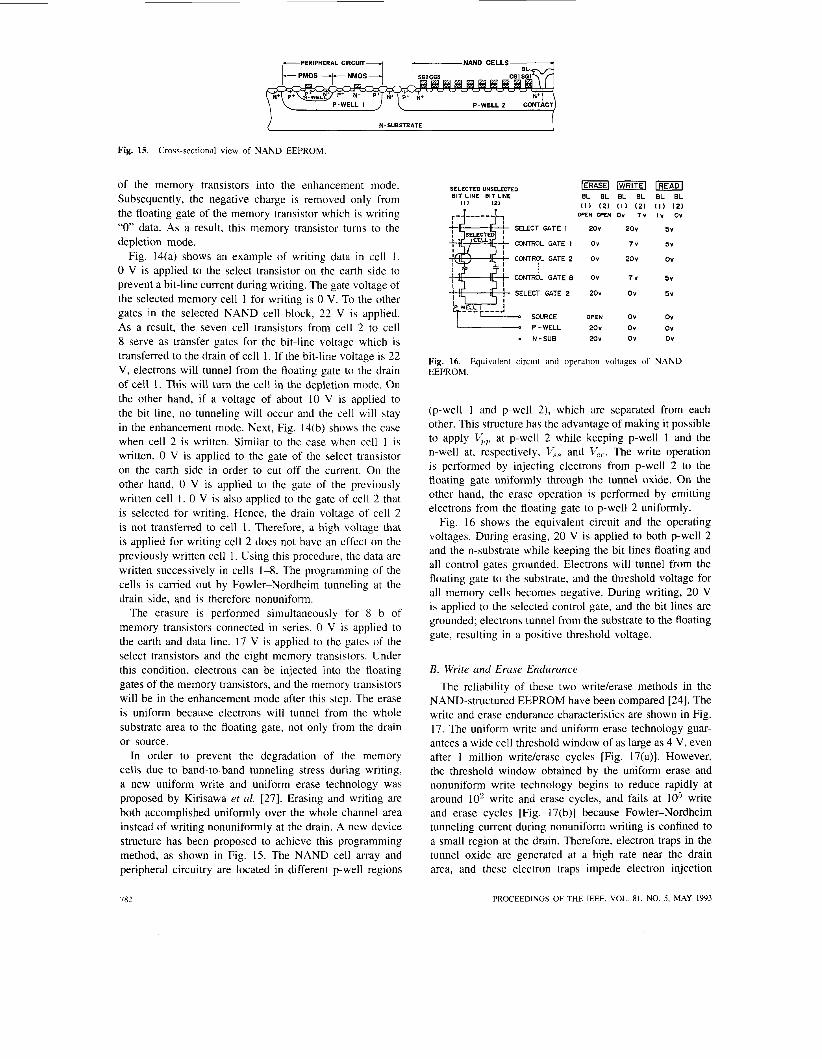
In order to prevent the degradation of the memory cells due to band-to-band tunneling stress during writing, a new uniform write and uniform erase technology was proposed by Kirisawa et al. [27]. Erasing and writing are both accomplished uniformly over the whole channel area instead of writing nonuniformly at the drain. A new device structure has been proposed to achieve this programming method, as shown in Fig. 15. The NAND cell array and peripheral circuitry are located in different p-well regions
[EiSq IWRITE] SELECTED UNSNCTED BIT LINE BIT LINE EL EL BL EL
( 1 ) ( 2 ) ( I ) ( 2 ) OPEN WW Ov 7 v
SaECT GATE I ZOv 2 0 v
C C ” L GATE I Ov 7 V
CCNTti?L GATE2 Ov 2 0 v
7 v
SELECT U T E 2 20v Ov
I I -H d GATE 8 Ov
SOURCE OPEN OV - P-WELL 2 0 v Ov
20v o v N-SUB
lREnol EL BL ( 1 ) ( 2 ) I v o v
5 v
5 v
o v
5 v
5 v
o v
o v ov
Fig. 16. EEPROM.
Equivalent circuit and operation voltages of NAND
(p-well 1 and p-well 2) , which are separated from each other. This structure has the advantage of making it possible to apply V’, at p-well 2 while keeping p-well 1 and the n-well at, respectively, Vqs and Vcc. The write operation is performed by injecting electrons from p-well 2 to the floating gate uniformly through the tunnel oxide. On the other hand, the erase operation is performed by emitting electrons from the floating gate to p-well 2 uniformly.
Fig. 16 shows the equivalent circuit and the operating voltages. During erasing, 20 V is applied to both p-well 2 and the n-substrate while keeping the bit lines floating and all control gates grounded. Electrons will tunnel from the floating gate to the substrate, and the threshold voltage for all memory cells becomes negative. During writing, 20 V is applied to the selected control gate, and the bit lines are grounded; electrons tunnel from the substrate to the floating gate, resulting in a positive threshold voltage.
B. Write and Erase Endurance The reliability of these two write/erase methods in the
NAND-structured EEPROM have been compared [24]. The write and erase endurance characteristics are shown in Fig. 17. The uniform write and uniform erase technology guar- antees a wide cell threshold window of as large as 4 V, even after 1 million write/erase cycles [Fig. 17(a)]. However, the threshold window obtained by the uniform erase and nonuniform write technology begins to reduce rapidly at around lo2 write and erase cycles, and fails at 10’ write and erase cycles [Fig. 17(b)] because Fowler-Nordheim tunneling current during nonuniform writing is confined to a small region at the drain. Therefore, electron traps in the tunnel oxide are generated at a high rate near the drain area, and these electron traps impede electron injection
782 PROCEEDINGS OF THE IEEE, VOL. 81, NO. 5, MAY 1993

6 , , , , , , , UNIFORM WRITE 17 7V.z~"-
4 UNIFORM E R A S 2 0 5 V . Z m ~ c NCt-UUIFORM ERASE 1 5 2 V , Z m r e c 3W'C
ERASE -4 - 4
-6 I IO io2 io3 IO' io5 io6 IO'
W/ E Cycles W/E Cycles
3°C I
( 0 ) UNIFORM WRITE AND (b) UNIFORM WRITE AND UNIFWM ERASE TECHNOLOGY NON-UNIFORM ERASE TECHNOLOGY
2 n
Fig. 17. Endurance characteristics.
TECHNOCffiY 4
and emission between the floating gate and substrate. This effect may be aggravated by hot holes that are generated by band-to-band tunneling.
In uniform write and uniform erase technology, the threshold voltage of the erased cell is dependent on the number of write/erase cycles. However, the threshold volt- age of the written cell is not dependent on the number of write/erase cycles. This can be explained as follows. The oxide traps and interface traps are generated uniformly over the entire channel area because Fowler-Nordheim tunneling of electrons is performed uniformly during both the writing and erasing operation. The uniformly trapped oxide charges over the channel area affect not only the electron tunneling current through the oxide, but also the flatband voltage. The threshold voltage of the erased cell decreases slightly up to lo3 cycles due to hole trapping. Hole traps affect the increase of stored positive charge on the floating gate as well as the decrease of the flatband voltage. After 103-106 cycles, the threshold voltage of the erased cell increases due to electron detrapping. On the other hand, the threshold voltage of the written cell remains almost constant up to IO6 cycles in spite of charge trapping in the oxide because the influence of stored charge on the floating gate and trapped oxide charge on both the flatband voltage and injection field cancel each other out [48].
C. Data Retention Data retention characteristics of the memory cell pro-
grammed by the two write and erase technologies measured at 300°C after different numbers of write and erase cycles from 10 to IO6 were carried out (Fig. 18). In the case of uniform erase and nonuniform write technology, the stored positive charges gradually decay as baking time increases, so the threshold window decreases [Fig. 18(b)]. However, in the case of uniform write and uniform erase technology, the stored positive charges effectively increase up to 100 min baking time due to the detrapping of electrons from the gate oxide to the substrate during the retention bake [Fig. 18(a)]. This increase of effectively stored positive charges up to 100 min retention bake becomes larger with an increasing number of cycles because the number of trapped negative charges in the thin oxide increases.
The effect of detrapping electrons is equivalent to the effect of trapping holes in the gate oxide. As a result, the detrapping of the electrons suppresses the data loss of
W/E Cycles
-3
RETENTION BAKE TIME (minl RETENTION BAKE TIME lminl
( a ) UNIFORM WRITE AND Ib) UNIFORM WRITE AND UNIFORM ERASE TECHNOLDGY NON-UNIFORM ERASE TECHNou)(M
Fig. 18. Data retention characteristics.
the positively charged cell. As a result, the stored positive charges which are effectively increasing at the beginning of the bake extend the data retention time of the memory cell programmed by the uniform write and uniform erase. Fig. 19 shows the data retention time after write and erase cycling. The data retention time can be extended by using uniform write and uniform erase technology, especially beyond IO5 write and erase cycles.
v. AND THE INTERPOLY DIELECTRICS
RELIABILITY OF THE TUNNEL OXIDE
A. Stress-Induced Oxide Leakage Current The reliability of the tunnel oxide is very important
for Flash EEPROM's. These devices are programmed and erased by high-field (Fowler-Nordheim) injection of elec- trons in a very thin dielectric film to charge and discharge the floating gate. Unfortunately, this current through the oxide degrades the quality of the oxide and eventually leads to breakdown. The wearout of tunnel oxide films during a high-field stress has been correlated with the buildup of both positive or negative trapped charges.
Recently, it has been shown that high-field stress also induces a low-field leakage current in thin oxides [40], [41], with a thickness less than 10 nm. The mechanism of this leakage current has been attributed to the generation of localized defects or weak spots [40] and trap states near
ARITOME Cf ( I / RELIABILITY ISSUES OF FLASH MEMORY CELLS 783

(a)Bi-pdority Stress (b)El&mn Emitted Stress (c)Electran Injected Stress
Fig. 20. (b) electron-emitted stress, and (c) electron-injected stress.
Setup and stressing waveform for (a) bipolarity stress,
the injecting interface [41], [42]. These low-field leakage currents degrade the data retention of the EEPROM cell [41], [43], [31]. Unfortunately, these oxide leakage currents increase with decreasing oxide thickness [401, [431, and make it difficult to scale down the oxide thickness of the memory cell.
Aritome et al. [3 11 studied the influence of the waveform of the stress voltage on the degradation of the tunnel oxide. Three types of high-field dynamic stress were used to study the thin oxide leakage currents. Fig. 20 shows the applied dynamic stress waveforms. In the case of bipolarity stress, positive high voltages are applied to the gate or to the substrate and source/drain ( Y D ) regions. Fowler-Nordheim tunneling occurs both from the substrate to the gate and from the gate to the substrate alternately. Electron-emitted stress, emission of electrons from the gate and electron- injected stress, emission of electrons from the substrate are performed for comparison. .The applied gate voltage is comparable to the floating-gate voltage of a memory cell during the write operation. The substrate voltage (V5nb) is chosen in such a way that the tunnel current during emitted and injected stress is the same.
The Ig-Vg characteristics before and after dynamic stress for a 5.6 nm oxide thickness are shown in Fig. 21. The thin oxide leakage currents subjected to three types of high-field dynamic stressing are compared. It is observed that the thin oxide leakage current induced by bipolarity stress is about one order of magnitude smaller than that induced by both the electron-emitted stress and the electron-injected stress. This result shows that the origin of the thin oxide leakage current can be suppressed by a reverse high-field stress.
The data retention characteristics of the Flash memory cell programmed by two different write/erase ( W E ) tech- nologies are compared [31]. Fig. 22 shows these two W E technologies. First, we have the bipolarity W E technology, which is a uniform write and erase technology. During the write operation, a high voltage (Vcq) is applied to the control gate, with the substrate and source/drain regions grounded. Electrons are injected from the substrate to the floating gate over the whole channel area of the memory cell. In the erase operation, a high voltage (Vsul,) is applied to the substrate
10-4 N TOX =5.6nm -
STRESS IO' cycles
Bi-polarity stress
" l O - ' P + + k Y Y + o ELECTRIC FIELD (MVIcm)
Fig. 21. Leakage current of the thin oxide at low voltages for 5.6 nm oxide after bipolarity stress, electron-emitted stress, and electron-injected stress.
W R I T E ERASE ((Electron ~ Injection11 .. (Electron Emission)/ OXIDE
Bi-polarity FN-t
Wr i te/Erase
technology
Bi-polarity Stress
Electron Emitted
Stress
Fig. 22. Comparison between (a) bipolarity F-N tunneling write/erase technology and (b) channel-hot-electron (CHE) write and F-N tunneling erase technology.
and source/drain regions, with the control gate grounded. Electrons are then emitted from the floating gate to the substrate. In this write/erase method, the high-field stress of the thin oxide corresponds to bipolarity stress. The other write/erase method is a channel hot electron (CHE) write and F-N tunneling erase technology. This technology is a nonuniform write and uniform erase technology. The erase operation is the same as in the bipolarity W E technology. However, during the write operation, high voltages are applied to the control gate and the drain. Thus, channel hot electrons are generated by the lateral electric field, and electrons are injected from the substrate to the floating gate. In this case, the high-field stress of the thin oxide is electron-emitted stress. The data retention will be different between these W E technologies because the thin oxide leakage current is different between the bipolarity stress and the electron-emitted stress of the thin oxide. Moreover, in the conventional erasing method of Flash memories [ 121, a high voltage is applied to the source. However, in our experiment, a high voltage is applied to the substrate as well as the source/drain regions in order to prevent the degradation of the thin oxide due to hole injection caused by band-to-band tunneling [ 121.
Fig. 23 shows the write and erase endurance character- istics of both W E technologies. No closure of the cell threshold window occurs up to 10' write/erase cycles in both technologies.
7x4 PROCEEDINGS OF THE IEEE. VOL. X I . NO. 5. MAY 1993

6
- 4 I > =75 nm --o--Bi-polarity FN-t writetamre technobgy
-*--E write and FN-t erose technohqy
io7 I
- 2 k ~ - + w - ~ ~ - . - e e d ERASE
t- -4
I IO io2 io3 lo4 lo5 lo6 107
WRITEIERASE CYCLES
Eo, = 6 MV/cm
Bi-polarity FN-t - Write/Erase
Fig. 23. cell with 7.5 nm oxide.
Write/erase endurance characteristics of Flash memory
-41 ' ' ' I I , I I
Initial' I IO IO' 103 104 105
RETENTION TIME (sec)
Fig. 24. Data retention characteristics under gate voltage stress for bipolarity F-N tunneling write/erase technology and channel hot electron (CHE) write and F-N tunneling erase technology.
Data retention characteristics are measured under various gate voltage conditions in order to accelerate the retention test. The memory cells are subjected to 10: write/erase cycles. In the case of the CHE write and F-N tunneling erase technology, the stored positive charges rapidly decay as a function of time; as a result, the threshold window decreases (Fig. 24). However, in the case of the bipolarity F-N tunneling W E technology, data loss of the stored positive charge is significantly reduced. This phenomenon can be explained by the fact that the thin oxide leakage current is reduced by the bipolarity F-N tunneling stress.
Fig. 25 shows the data retention time after write and erase cycling as a function of the tunnel oxide thickness. The data retention time is defined by the time that Vtll reaches -1.0 V during the gate voltage stress. In devices with a 7.5 nm tunnel oxide, the data retention time obtained with the bipolarity F-N tunneling write/erase technology is 50 times longer than that of CHE write and F-N tunneling erase technology after 10' cycles. However, in devices with a 9 nm tunnel oxide thickness, the data retention time is almost the same for both technologies. For very thin (<9 nm) tunnel oxides, the bipolarity write/erase technology offers improved data retention times in comparison with the CHE write and F-N tunneling erase technology. Therefore, this technology may facilitate the down-scaling of the tunnel oxides. Reducing the tunnel oxide thickness results in lower programming voltages and in faster read operations because the read current is increased.
CHE wite and I FN-t erase I , , , t e c y
6 7 8 9 1 0 102
OXIDE THICKNESS (nm)
Fig. 25. Data retention time of Flash memory cell after write and erase cycling as a function of tunnel oxide thickness. The data retention time is defined by the time at which lit, reaches -1.0 V during the applied gate voltage stress.
c 1 10 bipolar stress I I g 102
; 10'
m . E o x = l 2 Mv/cm
Frequency ( Hz) DC i o o i o ' i o 2 i o 3 i o 4 i o i o 6 10'
E 100
F
Fig. 26. Dependence of time-to-breakdown on stress drequency.
B. Time-Dependent Dielectric Breakdown Under High-Frequency Stress
The time-dependent dielectric breakdown (TDDB) char- acteristics of the tunnel oxide will be discussed here. In particular, it will be shown that TDDB characteristics are dependent on the stress wave form and its frequency.
Fig. 26 shows that the TDDB characteristics [44], [45] depend on both the stress waveform and its frequency. The stress waveforms are the electron-emitted stress, the electron-injected stress, and the bipolarity stress. The time to breakdown during bipolarity stress is longer than that during both the electron-emitted stress and the electron- injected stress. Moreover, it is shown that the TDDB characteristics depend on the frequency of the stress wave. The breakdown time under unipolarity stress does not depend on frequency. However, the breakdown time of bipolarity stress strongly depends on the frequency. The bipolarity stress lifetime in the megahertz range is about 40 times higher than that at 10 Hz at the same applied voltage. It is suggested in [45] that the improved TDDB
ARITOME er 01.: RELIABILITY ISSUES OF FLASH MEMORY CELLS 785

obtained with the bipolarity stress is due to the field-assisted detrapping of holes at the Si/SiO2 interface.
C. Interpoly Dielectrics ONO (oxide/nitride/oxide) interpoly dielectrics are cur-
rently used for nonvolatile memories. In the case of non- volatile memories, the important issues are not only low defect density and long mean time to failure, but also charge retention capability. Mori et al. investigated the ONO inter- poly dielectrics thickness scaling effect on charge retention characteristics in nonvolatile memories systematically [49].
For the top oxide layer, a certain thickness (3 nm) of top oxide, which can block the hole injection, is required. SIN thickness reduction leads to reduced initial rapid charge loss. However, too much reduction sometimes leads to en- hanced charge loss in the long bake test. Bottom polyoxide thinning, down to 10 nm, does not result in degradation. The NO (nitrideloxide) double-layer structure shows a large initial rapid charge loss, which may be prevented by applying the ONO structure. However, if the bottom oxide layer is thin and its quality is poor, a part of the bits may suffer from rapid initial charge loss. When scaling down the ONO thickness, one must consider these key factors concerning charge retention as well as dielectric reliability.
VI. CONCLUSIONS Reliability issues of Flash EEPROM’s are reviewed. The
reliability of both the sourcexrase type (ETOX) Flash memory and the NAND structure EEPROM have been discussed. Disturbs during programming, write/erase en- durance, and charge loss of both devices are reviewed. The reliability of the tunnel oxide and the interpoly di- electric have also been addressed. The bipolarity F-N programming/erase, which is used in the NAND EEPROM, improves the charge to breakdown ( Q b d ) and decreases the stress-induced leakage current. Therefore, the bipolarity write/erase method is very promising for application in future Flash EEPROM devices.
VII. ACKNOWLEDGMENT The authors would like to thank R. Kirisawa, R.
Nakayama, T. Yamaguchi, T. Hatakeyama, S. Iizuka, S. Shutoh, M. Momodomi, T. Tanaka, Y. Tanaka, H. Nakamura, H. Oodaira, S. Watanabe, and K. Ohuchi for their helpful discussion on this work.
REFERENCES
[I ] F. Masuoka, M. Asano, H. Iwahashi, T. Komuro and S. Tanaka, “A new Flash EEPROM cell using triple polysilicon technol- ogy,” in IEEE Tech. Dig. IEDM 1984, pp. 464467 .
[2] -, “A 256K Flash EEPROM using triple polysilicon technol- ogy,” in IEEE ISSCC 1985, pp. 168-169.
[31 -, “A 256K Flash EEPROM using triple polysilicon tech- nology,” IEEE J. Solid-Stare Circuits, vol. SC-22, pp. 548-552, Aug. 1987.
[4] S . Mukherjee, T. Chang, R. Pan, M. Knecht, and D. Hu, “A single transistor EEPROM cell and its implementation in a 5 12K CMOS EEPROM,” in IEEE Tech. Dig. IEDM 1985, pp. 6 1 6-6 1 9.
. .
786
[SI G. Samachisa, C. S . Su, Y. S . Kao, G. Smarandoiu, T. Wong, and C. Hu, “A 128K Flash EEPROM using double polisilicon technology,” in IEEE ISSCC 1987, pp. 76-77.
[6] G. Samachisa, C. S. Su, Y. S . Kao, G. Smarandoiu, C. Y. M. Wang, T. Wong, and C. Hu, “A 128K Flash EEPROM using double polisilicon technology,” IEEE J Solid-State Circuits, vol.
[7] F. Masuoka, M. Momodomi, Y. Iwata, and R. Shirota, “New ultra high density EPROM and Flash EEPROM cell with NAND structure cell,” in IEEE Tech. Dig. IEDM 1987, pp.
[8] H. Kume, H. Yamamoto, T. Adachi, T. Hagiwara, K. Komori, T. Nishimoto, A. Koike, S. Meguro, T. Hayashida, and T. Tsukada, “A flash-erase EEPROM cell with an asymmetric source and drain structure,” in IEEE Tech. Dig. IEDM 1987, pp. 560-563.
[9] V. N. Kynett, A. Baker, M. Fandrich, G. Hoekstra, 0. Jungroth, J. Kreifels, and S. Wells, “An in-system reprogrammable 256K CMOS flash memory,’’ in IEEE ISSCC 1988, pp. 132-133.
IO] V. N. Kynett, A. Baker, M. Fandrich, G . Hoekstra, 0. Jungroth, J. Kreifels, S . Wells, and M. Winston, “An in-system repro- grammable 32KX8 CMOS flash memory,’’ IEEE J. Solid-state Circuits, vol. 23, pp. 1157-1 162, Oct. 1988.
1 I] R. Shirota, Y. Itoh, R. Nakayama, M. Momodomi, S . Inoue, R. Kirisawa, Y. Iwata, M. Chiba, and F. Masuoka, “A new NAND cell for ultra high density 5V-only EEPROMs,” in 1988 Symp. VLSI Technol., Tech. Paper, pp. 33-34.
121 S. Tam, S . Sachdev, M. Chi, G. Verma, J . Ziller, G. Tsau, S . Lai, and V. Dham, “A high density CMOS I-T electrically erasable non-volatile (Flash) memory technology,” in 1988 Symp. VLSI Technof., Tech. Paper, pp. 31-32.
[I31 G. Verma, and N. Mielke, “Reliability performance of ETOX based Flash memories,” in Proc. IEEE IRPS 1988, pp. 158-166.
[I41 M. Momodomi, R. Kirisawa, R. Nakayama, S . Aritome, T. Endoh, Y. Itoh, Y. Iwata, H. Oodaira, T. Tanaka, M. Chiba, R. Shirota and F. Masuoka, “New device technologies for 5V- only 4Mb EEPROM with NAND structure cell,” in IEEE Tech. Dig. IEDM 1988, pp. 412415 .
[I51 R. Kazerounian, S. All, Y. Ma, and B. Eitan, “A 5 Volt high density poly-poly erase flash EPROM cell,” in IEEE Tech. Dig. IEDM 1988, pp. 436439 .
[I61 M. Gill, R. Cleavelin, S . Lin, I. D.’Anigo, G. Santin, P. Shah, A. Nguyen, J. Esquivel, B. Riemenschneider, and J. Paterson, “A 5-volt contactless array 256k flash EEPROM technology,” in IEEE Tech. Dig. IEDM 1988, pp. 428431 .
[I71 S. D’Arrigo, G. Imondi, G. Santin, M. Gill, R. Cleavelin, S. Spagliccia, E. Tomasetti, S . Lin, A. Nguyen, P. Shah, G. Savarese, and D. McElroy, “A 5V-only 256k bit CMOS flash EEPROM,” in IEEE ISSCC 1989, pp. 132-133.
[IS] S. Haddad, C. Chang, B. Swaminathan, and J. Lien, “Degrada- tion due to hole trapping in flash memory cells,” IEEE Electron Device Lett., vol. 10, pp. 1 17-1 19, Mar. 1989.
[I91 M. Momodomi, Y. Itoh, R. Shirota, Y. Iwata, R. Nakayama, R. Kirisawa, T. Tanaka, S. Aritome, T. Endoh, K. Ohuchi, and F. Masuoka, “An experimental 4-Mbit CMOS EEPROM with a NAND structure cell,” IEEE J. Solid-State Circuits, vol. 24,
[20] V. N. Kynett, M. Fandrich, J. Anderson, P. Dix, 0. Jungroth, J. Kreifels, R. A. Lodenquai, B. Vajdic, S . Wells, M. Winston, and L. Yang, “A 90-11s one-million erase/program cycle I-Mbit flash memory,” IEEE J. Solid-State Circuits, vol. 24, pp. 1259-1264, Oct. 1989.
[21] K. Naruke, S . Yamada, E. Obi, S . Taguchi, and M. Wada, “A new flash erase EEPROM cell with sidewall select-gate on its source side,” in IEEE Tech. Dig. IEDM 1989, pp. 603-606.
[22] M. Gill, R. Cleavelin, S . Lin, I. D’Arrigo, G. Santin, P. Shah, A. Nguyen, R. Lahily, P. DeSimone, G. Piva, and J. Paterson, “A 5-volt only flash EEPROM technology for high density memory and system IC applications,” in IEEE 1989 CICC.
[23] T. Endoh, R. Shirota, Y. Tanaka, R. Nakayama, R. Kirisawa, S. Aritome, and F. Masuoka, “New design technology for EEPROM memory cells with 10 million writelerase cycling endurance,” in IEEE Tech. Dig. IEDM 1989, pp. 599-602.
[24] S. Aritome, R. Kirisawa, T. Endoh, N. Nakayama, R. Shirota, K. Sakui, K. Ohuchi, and F. Masuoka, “Extended data retention characteristics after more than 10‘ write and erase cycles in EEPROMs,” in IEEE IRPS 1990, pp. 259-264.
[25] Y. Iwata, M. Momodomi, T. Tanaka, H. Oodaira, Y. Itoh, R. Nakayama, R. Kirisawa, S . Aritome, T. Endoh, R. Shirota, K.
SC-22, pp. 676-683, Oct. 1987.
552-5155,
pp. 1238-1243, Oct. 1989.
PROCEEDINGS OF THE IEEE. VOL. X I , NO. 5 , MAY 1993

Ohuchi, and F. Masuoka, “A high-density NAND EEPROM with block-page programming for microcomputer applications,” IEEE J . Solid-State Circuits, vol. 25, pp. 417424, Apr. 1990. B. Riemenschneider. A. L. Esquivel, J. Paterson, M. Gill, S. Lin, D. McElroy, P. Truong, R. Bussey, B. Ashmore, M. McConnell, H. Stiegler, and P. Shah, “A process technology for a 5-volt only 4Mb flash EEPROM with an 8.6 bm2 cell,” in IEEE 1990 Symp. VLSI Technol., pp. 125-126. R. Kirisawa, S. Aritome, R. Nakayama, T . Endoh, R. Shirota, and F. Masuoka, “A NAND structured cell with a new program- ming technology for highly reliable SV-only Flash EEPROM,” in 1990 Symp. VLSI Techno/., Tech. Paper, pp. 129-130. B. J. Woo, T. C. Ong, A. Fazio, C. Park, G. Atwood, M. Holler, S. Tam, and S. Lai, “A novel memory cell using flash array contactless EPROM(FACE) technology,” in IEEE Tech. Dig. IEDM 1990, pp. 91-94. N. Ajika, M. Ohi, H. Arima, T. Matsukawa, and N. Tsubouchi, “A 5 volt only 16M bit flash EEPROM cell with a simple stacked gate structure,” in IEEE Tech. Dig. IEDM 1990, pp. 115-1 18. M. Gill, R. Cleavelin, S. Lin, M. Middendorf, A. Nguyen, J. Wong, B. Huber, S. D.’Amgo, P. Shah, E. Kougianos, P. Hefley, G. Satin, and G. Naso, “A novel sublithographic tunnel diode based bolt flash memory,” in IEEE Tech. Dig. IEDM 1990, pp. 119-122. S. Aritome, S. Shirota, R. Kirisawa, T . Endoh, N. Nakayama, K. Sakui, and F. Masuoka, “A reliable bi-polarity write/erase technology in flash EEPROMs,” in IEEE Tech. Dig. IEDM 1990, DD. 111-114.
[47] N. R. Mielke, “New EPROM data-loss mechanisms,” in Proc. IRPS 1983, pp. 10&113.
[48] J. S. Witters, G. Groeseneken, and H. E. Maes, “Degradation of tunnel-oxide floating-gate EEPROM devices and the correlation with high field-current-induced degradation of thin gate oxide,” IEEE Trans. Electron Devices, vol. 36, pp. 1663-1682, Sept. 1989.
[49] S. Mori, E. Sakagami, H. Araki, Y. Kaneko, K. Narita, Y. Ohshima, N. Arai, and K. Yoshikawa, “ONO inter-poly dielec- tric scaling for nonvolatile memory applications,” IEEE Trans. Electron Devices, vol. 38, pp. 386-391, Feb. 1991.
Seiichi Aritome was born in Hiroshima, Japan, on August 9, 1960 He received the B E and M.E degrees in electronic engineering from Hiroshima University, Japan, in 1983 and 1985, respectively
He joined the Toshiba Research and Develop- ment Center, Kawasaki, Japan, in 1985 Since then he has been engaged in the development of high-density DRAM’s and EEPROM’s at the Toshiba ULSI Re\earch Center
Mr Aritome I F a member of the Japan Society of Applied Physics.
[32] B. J. Woo, T. C. Ong, and S Lai, “A poly-buffered FACE technology for high density flash memories,” in 1991 S m p . VLSI Technol., Tech Paper, pp. 73-74.
[33] N. Kodama, K. Saitoh, H Shirai, T. Okazaki, and Y Hokari, “A 5V only 16Mbit flash EEPROM cell using highly reliable write/erase technologies,” in 1991 Symp. VLSI Technol., Tech. Paper, pp. 75-76.
[34] H. Kume, T. Tanaka, T Adachi, N. Miyamoto, S. Saeki, Y. ohji, M. Ushiyama, T. Kobaya\hi, T. Nishida, Y. Kawamoto, and K. Seiki, “A 3 42 pm’ flash memory cell technology comformable to sector erase,” in 1991 Sbmp. VLSl Technol, Tech. Paper, pp. 77-78
[35] K. Yoshikawa, S. Mori, E. Sakagami, N Arai, Y Kaneko, and Y. Ohshima, “Flash EEPROM cell scaling based on tunnel oxide thinning limitations,” in 1991 Symp. VLSl Technol, Tech Paper, pp 79-80.
[36] S. Yamada, T Suzuki, E. Obi, M. Oshikiri, K Naruke, and M Wada, “A self-convergence erasing scheme for a simple stacked gate flash EEPROM,” in IEEE Tech Dig. IEDM 1991, pp. 307-310.
[37] D C. Guterman, I H Rimawi, R D. Halvorson, D J. McElroy, and W. W. Chan, “Electrically alterable hot-electron injection floating gate MOS memory cell with series enhancement,” in IEEE Tech. Dig. IEDM 1978, pp. 340-343.
[38] J. Chen, T. Y. Chan, I. C. Chen, P. K. KO, and C Hu, “Subbreakdown drain leakage current in MOSFET,” IEEE Electron Device Let t , vol. EDL-8, pp. 5 15-5 17. Nov 1987
[39] C Chang and J Lien, “Comer-field induced drain leakage in thin oxide MOSFETs,” in IEEE Tech Dig IEDM 1987. pp. 7 14-7 17.
[40] P. Olive, T N. Nguyen, and B. Ricco, “High-field-induced degradation in ultra-thin Si02 films,” IEEE Tran5 Elecfron Devices, vol. 35, pp 2259-2267, Dec. 1988.
[41] D A Baglee and M C Smayling, “The effects of write/erase cycling on data loss in EEPROM\,” in IEEE Tech Dig IEDM 1985, pp. 624-626.
[42] R Rofan and C. Hu, “Stress-induced oxide leakage,” IEEE Electron Devrce L e f t , vol. 12, pp. 632-634, Nov 1991.
[43] K. Naruke. S. Taguchi, and M Wada, “Stress induced leak- age current limiting to scale down EEPROM tunnel oxide thicknes,” in IEEE Tech. Dig IEDM 1988, pp 4 2 4 4 2 7
(441 E. Rosenbaum and C Hu, “High-frequency time-dependent breakdown of SiO2,” IEEE Electron Device L e u , vol 12. pp 267-269, June 1991
[45] E. Rosenbaum, Z Liu, and C. Hu, “The effect of oxide \tress waveform on MOSFET performance,” in IEEE Tech Dig.
[46] R. E Shiner, J. M. Caywood, and B. L Euzent, “Data retention in EPROMs,” in Proc. IRPS 1980, pp 238-243
vice9 in general, hot ele, degradation
lEDM 1991. pp 719-722
Riichiro Shirota was born in Hyogo, Japan, on February 22, 1954. He received the B.E., M.E., and Ph.D. degrees in physics in 1977, 1979, and 1982, respectively, from Nagoya University.
He joined the Toshiba Corporation, Kawasaki, Japan, in 1982. Since then he has been engaged in research and development of high-density DRAM’s and EEPROM’s at the Thoshiba ULSI Research Center.
Gertjan Hemink w’as born in The Netherlands in 1964. He received the M.Sc. and Ph.D. de- grees in electrical engineering from the Univer- sity of Twente in 1988 and 1992, respectively.
At the University of Twente he worked on the development and application of nonvolatile memory cells with a buried injector structure. In July 1992 he joined the Device Research Department of the Toshiba Research and De- velopment Center, Kawasaki, Japan. His main research interests are nonvolatile memory de-
xron modeling, and the modeling of tunnel oxide
Tetsuo Endoh was born in Tokyo, Japan, on October 30, 1962. He received the B.S. degree in physics from the University of Tokyo, Japan, in 1987.
He joined the Toshiba Research and Develop- ment Center, Kawasaki, Japan, in 1987. Since then he has been engaged in research and de- velopment of high-density EEPROM’s at the Toshiba ULSI Research Center.
AXITOME er al.: RELIABILITY ISSUES OF FLASH MEMORY CELLS 7x7

I!!!?? " .-
Fujio Masuoka was born in Takasaki, Japan, on May 9, 1943. He received the B.E., M.E., and Ph.D. degrees in electrical engineering from Tohoku University. Sendai, Japan, in 1966, 1968, and 1971, respectively.
In 1971 he joined the Toshiba Research and Development Center, Toshiba Corporation, Kawasaki, Japan, where he has been working on MOS LSI memory. He is currently managing the Device Research Department of Toshiba ULSI Research Center. His research interests have
been in memory cells such as EPROM, EEPROM, MROM, SRAM, and DRAM.
Dr. Masuoka received the Watanabe Award and the National Invention Award in 1977 and 1978, respectively. He is a member of the Institute of Electronics, Information, and Communication Engineers of Japan.
7xx PROCEEDINGS OF THE IEEE. VOL. X I , NO. 5. MAY 1993
1