reliable 3-d clock-tree synthesis considering nonlinear
TRANSCRIPT

1734 IEEE TRANSACTIONS ON COMPUTER-AIDED DESIGN OF INTEGRATED CIRCUITS AND SYSTEMS, VOL. 32, NO. 11, NOVEMBER 2013
Reliable 3-D Clock-Tree Synthesis ConsideringNonlinear Capacitive TSV Model With
Electrical–Thermal–Mechanical CouplingSai Manoj P. D., Student Member, IEEE, Hao Yu, Member, IEEE, Yang Shang, Student Member, IEEE,
Chuan Seng Tan, Member, IEEE, and Sung Kyu Lim, Senior Member, IEEE
Abstract—A robust physical design of 3-D IC requires inves-tigation on through-silicon via (TSV). The large temperaturesand stress gradients can severely affect TSV delay with largevariation. The traditional physical model treats TSV as a resistorwith linear electrical–thermal dependence, which ignores the fun-damental device physics. In this paper, a physics-based electrical–thermal–mechanical delay model is developed for signal TSVs in3-D IC. With consideration of liner material and also stress, anonlinear model is established between electrical delay with tem-perature and stress. Moreover, sensitivity analysis is performedto relate the reduction of temperature and stress gradients withrespect to dummy TSVs insertion. Taking the design of 3-Dclock tree as a case study, we have formulated a nonlinearoptimization problem for clock-skew reduction. By allocatingdummy TSVs to reduce the temperature and stress gradients,the clock skew introduced by signal TSVs and drivers can beminimized. A number of 3-D clock-tree benchmarks are utilizedin experiments. We have observed that with the use of dummyTSV insertion, clock skew can be reduced by 61.3% on averagewhen the accurate nonlinear electrical–thermal–mechanical delaymodel is applied.
Index Terms—Clock-skew reduction, electrical–thermal–mechanical coupling, nonlinear MOSCAP, stress gradient,temperature gradient, thermal TSV, through-silicon via (TSV),TSV stress.
I. Introduction
3 -D INTEGRATED circuits (3-D ICs) have regained theinterest for big bandwidth in the design of many-core
microprocessor server. The utilization of through-silicon vias(TSVs) in 3-D IC can significantly reduce the latency andpower dissipation in global interconnect such as memory busesand also clock trees [1]–[18]. However, one robust 3-D ICdesign requires a careful examination of TSVs in which elec-trical states such as delays are coupled from multiple physicaldomains. First, thermal reliability is one primary concern since
Manuscript received February 22, 2013; revised April 13, 2013, May 15,2013; accepted June 9, 2013. Date of current version October 16, 2013. Thispaper was recommended by Associate Editor C.-N. Chu.
S. Manoj P. D., H. Yu, Y. Shang, and C. S. Tan are with theSchool of Electrical and Electronic Engineering, Nanyang Technologi-cal University 639798, Singapore (e-mail: [email protected];[email protected]; [email protected]; [email protected]).
S. K. Lim is with the School of Electrical and Computer Engineer-ing, Georgia Institute of Technology, Atlanta, GA 30332 USA (e-mail:[email protected]).
Color versions of one or more of the figures in this paper are availableonline at http://ieeexplore.ieee.org.
Digital Object Identifier 10.1109/TCAD.2013.2270285
heat sink has a long distance for the top layer. Moreover,dynamic voltage and frequency scaling of many-core can resultin highly nonuniform power density. As such, there exists alarge temperature gradient that can result in delay variation ofTSV by electrical–thermal coupling. What is more, becausecoefficients of thermal expansion (CTE) of TSV materialand substrate material are different, large mechanical stresscan be introduced, which in turn leads to delay variation ofdriver by electrical–mechanical coupling. Since delay variationintroduces skew for delay sensitive clock-tree design, a robustphysical design in 3-D IC with TSVs thereby needs to consideroptimization from coupled electrical, mechanical, and thermaldomains.
The design of clock tree is primarily involved with reduc-tion of delay difference at different sinks, known as skew[19]–[26]. Compared to clock tree in 2-D IC, the one in3-D IC will experience much larger temperatures and stressgradients both vertically and horizontally. As signal TSVsare deployed to route 3-D clock tree over the entire 3-Dchip, such nonuniform temperature differences can lead to asignificant clock skew by electrical–thermal coupling of signalTSVs [24]–[26]. Such an electrical–thermal coupling becomesnonlinear when liner material is considered. Moreover, theTSV-induced stress also affects the mobility and delay ofdrivers, which further worsens the clock skew over the entire3-D chip by electrical–mechanical coupling of drivers [10]. Assuch, the traditional clock-tree design methods [19]–[21] with-out considering temperature and stress gradients will becomeinaccurate and unreliable. The thermal-aware 3-D clock-treesynthesis has been discussed in [4] considering thermal profile.A 3-D embedding method was developed in [17] to reducethe wire length. Further optimization in [11] is developedto reduce power and slew rate. However, previous methodsonly conduct the clock network optimization based on linearor nonlinear electrical–thermal–mechanical coupling, ignoringthe TSV physical model and hence is not accurate. As such,there is no specific problem formulated for clock-tree designbased on the reduction of both thermal and stress gradients in3-D IC.
In this paper, based on recent measurement results in[6], [8], [10], [12], and [13], a nonlinear electrical–thermal–mechanical delay model is developed for 3-D clock-treedesign. Further, sensitivity analysis is performed for dummyTSV density with respect to reduction of temperature or stress
0278-0070 c© 2013 IEEE

MANOJ P.D. et al.: RELIABLE 3-D CLOCK-TREE SYNTHESIS CONSIDERING NONLINEAR CAPACITIVE TSV MODEL 1735
Fig. 1. Simplified TSV fabrication procedure.
gradient. Based on accurate TSV models, a reliable 3-D clock-tree design is formulated by dummy TSVs insertion to balancethe clock skew by reducing temperature and stress gradient,with consideration of nonlinear electrical–thermal–mechanicaldelay model. A nonlinear programming-based optimization isdeveloped and implemented to determine the allocation ofdummy TSVs. Experimental results show that with insertion ofa reasonable number of dummy TSVs, the average clock skewcan be reduced by 61.3% for clock-tree benchmarks in [27]in 3-D design [11]. Compared to clock-tree design by lineardelay model, our approach by nonlinear delay model reducesclock skew further by 12.2% under same thermal conditionsand same TSV density.
The rest of this paper is organized as follows. The reli-able 3-D clock-tree design problem formulation is discussedin Section II. Modeling of signal TSVs and drivers underelectrical–thermal–mechanical coupling is discussed in Sec-tion III, and the dummy TSV model and the sensitivity studyare discussed in Section IV. Section V discusses the nonlinearelectrical–thermal–mechanical delay and skew model. Non-linear optimization for reduction of clock skew is presentedin Section VI. Numerical experimental results for modelingand optimization are presented in Section VII. The paper isconcluded in Section VIII.
II. 3-D Reliable Clock-Tree Design Problem
Many approaches have been applied in 2-D clock-treedesigns to reduce clock skew such as buffer sizing [4], mergingpoint adjustment [22], and wire-length balancing [21]. Due tononuniform power densities by many-core microprocessors,there is a large nonuniform temperature gradient. Moreover, alarge stress gradient is induced by TSVs during annealing.Accordingly, the 3-D clock tree will experience significantclock skew under large temperature and stress gradients witha new problem formulation required.
A. TSV Fabrication
An accurate physical model of TSV needs a detailed in-vestigation on its fabrication. As shown in Fig. 1, TSVs areused as vertical interconnections between stacked dies forproviding electrical interconnect as well as heat dissipation.To perform these functions, the materials used for TSVsshould have good electrical conductivity as well as thermalconductivity. Tungsten (W), poly-silicon, and copper (Cu) canbe considered as TSV fill materials. Due to low resistivityand cost, copper is the widely used material for TSV fill [10].To fabricate TSVs, TSV etching is performed by deep ionreactive etching (DRIE), laser or chemical etching, etc. Afterthe etching is performed, the liner material is deposited toprevent ion particle diffusion. After forming the liner layer, theTSV material, such as copper or tungsten, is filled in the etchedregion at high temperature. After annealing to low temperature,
Fig. 2. 3-D clock-tree distribution network at different tiers. (a) Clock treewith 14 TSV bundle locations in an H-tree. (b) Clock tree with 28 TSV bundlelocations in an H-tree. (c) Layer configuration under nonuniform temperaturedistribution.
the substrate is thinned and the current layer can be aligned andintegrated with other layers. Due to the existence of liner andalso the annealing, the physical TSV model becomes electrical,thermal, and mechanical coupled.
B. Problem Formulation
3-D clock tree, as shown in Fig. 2, makes use of TSV forvertical interconnections, which can have significant delay. Assuch, in 3-D clock-tree design, unlike 2-D clock-tree synthesis,the impact of TSV also needs to be considered. Stacking ofdies in vertical direction in 3-D design increases the overalltemperature and also the temperature gradient, due to theincreased and nonuniform power density and heat-dissipationpath. Due to the temperature gradient, the device character-istics also vary because of electrical–thermal coupling. Thetemperature distribution on a 3-D clock tree is shown in Fig. 2.Normally, RC delay DRC for the traditional TSV is modeledas RC-interconnect by a linear electrical–thermal coupling
RT = R0(1 + α · δT ); DRC = R0C0(1 + α · δT ) (1)
where RT is thermal-dependent resistance, R0 represents resis-tance at room temperature, C0 represents capacitance at roomtemperature, δT is the difference of the operating temperatureT and room temperature T0. In addition, note that α is thetemperature-dependent coefficient for resistance, whose valueis experimentally determined.
However, due the existence of liner material around TSV-fill, it forms a nonlinear MOSCAP that can significantlyaffect TSV delay. According to the measurement results in[8], the contribution of second-order temperature-dependentcontribution in MOSCAP model is increased to 30% of theoverall TSV capacitance at 150 °C. As such, TSV needs tobe characterized as a capacitor with nonlinear temperature-dependent instead of linear temperature-dependent resistor.What is more, TSVs exert mechanical stress on the siliconsubstrate due to mismatched CTEs. The impact of stress canaffect mobility and delay of driver. Eventually, one needs anonlinear electrical–thermal–mechanical coupled delay modelin 3-D IC.
By considering all the aforementioned effects, delay at eachclock sink i of one 3-D clock tree needs to be modeled as a
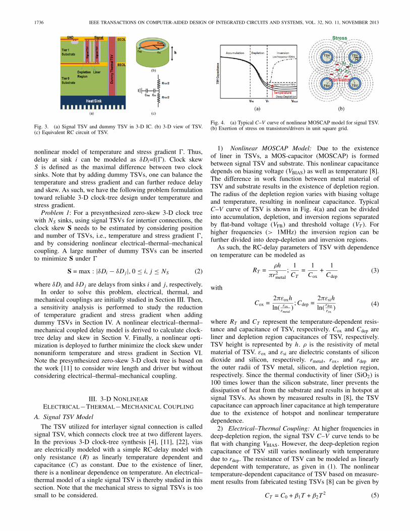
1736 IEEE TRANSACTIONS ON COMPUTER-AIDED DESIGN OF INTEGRATED CIRCUITS AND SYSTEMS, VOL. 32, NO. 11, NOVEMBER 2013
Fig. 3. (a) Signal TSV and dummy TSV in 3-D IC. (b) 3-D view of TSV.(c) Equivalent RC circuit of TSV.
nonlinear model of temperature and stress gradient �. Thus,delay at sink i can be modeled as δDi=f(�). Clock skewS is defined as the maximal difference between two clocksinks. Note that by adding dummy TSVs, one can balance thetemperature and stress gradient and can further reduce delayand skew. As such, we have the following problem formulationtoward reliable 3-D clock-tree design under temperature andstress gradient.
Problem 1: For a presynthesized zero-skew 3-D clock treewith NS sinks, using signal TSVs for intertier connections, theclock skew S needs to be estimated by considering positionand number of TSVs, i.e., temperature and stress gradient �,and by considering nonlinear electrical–thermal–mechanicalcoupling. A large number of dummy TSVs can be insertedto minimize S under �
S = max : |δDi − δDj|, 0 ≤ i, j ≤ NS (2)
where δDi and δDj are delays from sinks i and j, respectively.In order to solve this problem, electrical, thermal, and
mechanical couplings are initially studied in Section III. Then,a sensitivity analysis is performed to study the reductionof temperature gradient and stress gradient when addingdummy TSVs in Section IV. A nonlinear electrical–thermal–mechanical coupled delay model is derived to calculate clock-tree delay and skew in Section V. Finally, a nonlinear opti-mization is deployed to further minimize the clock skew undernonuniform temperature and stress gradient in Section VI.Note the presynthesized zero-skew 3-D clock tree is based onthe work [11] to consider wire length and driver but withoutconsidering electrical–thermal–mechanical coupling.
III. 3-D Nonlinear
Electrical−Thermal−Mechanical Coupling
A. Signal TSV Model
The TSV utilized for interlayer signal connection is calledsignal TSV, which connects clock tree at two different layers.In the previous 3-D clock-tree synthesis [4], [11], [22], viasare electrically modeled with a simple RC-delay model withonly resistance (R) as linearly temperature dependent andcapacitance (C) as constant. Due to the existence of liner,there is a nonlinear dependence on temperature. An electrical–thermal model of a single signal TSV is thereby studied in thissection. Note that the mechanical stress to signal TSVs is toosmall to be considered.
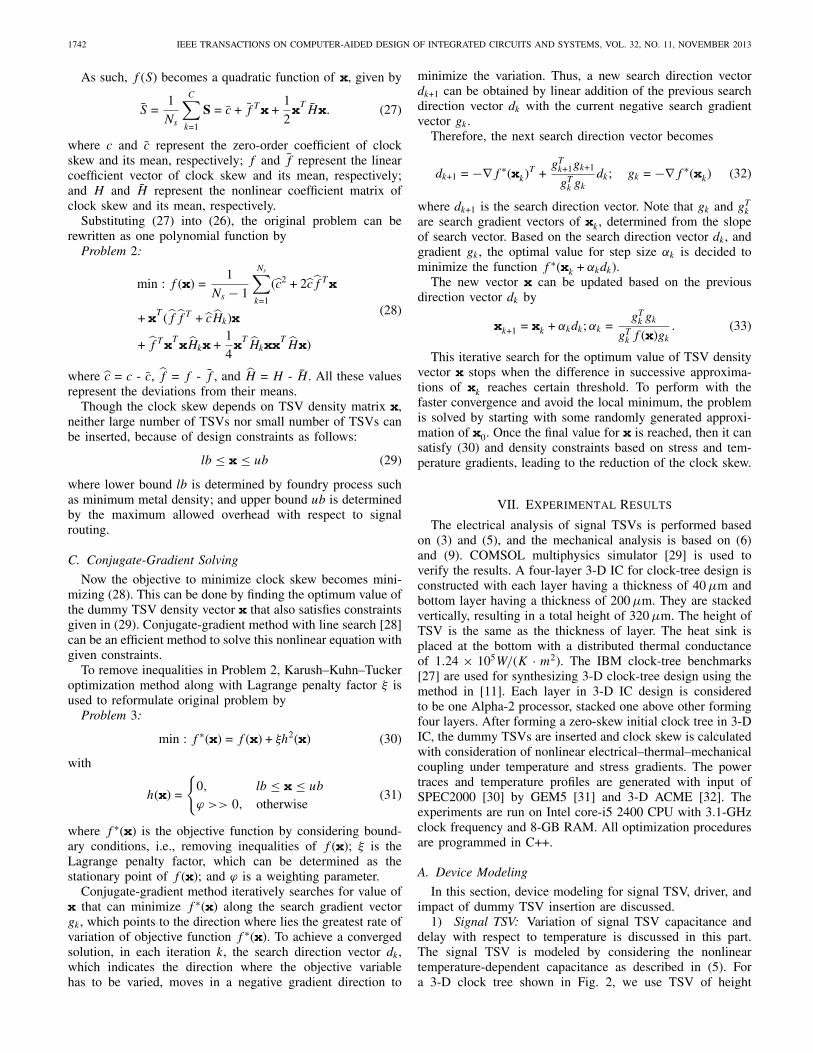
Fig. 4. (a) Typical C–V curve of nonlinear MOSCAP model for signal TSV.(b) Exertion of stress on transistors/drivers in unit square grid.
1) Nonlinear MOSCAP Model: Due to the existenceof liner in TSVs, a MOS-capacitor (MOSCAP) is formedbetween signal TSV and substrate. This nonlinear capacitancedepends on biasing voltage (VBIAS) as well as temperature [8].The difference in work function between metal material ofTSV and substrate results in the existence of depletion region.The radius of the depletion region varies with biasing voltageand temperature, resulting in nonlinear capacitance. TypicalC–V curve of TSV is shown in Fig. 4(a) and can be dividedinto accumulation, depletion, and inversion regions separatedby flat-band voltage (VFB) and threshold voltage (VT ). Forhigher frequencies (> 1MHz) the inversion region can befurther divided into deep-depletion and inversion regions.
As such, the RC-delay parameters of TSV with dependenceon temperature can be modeled as
RT =ρh
πr2metal
;1
CT
=1
Cox+
1
Cdep(3)
with
Cox =2πεoxh
ln( roxrmetal
); Cdep =
2πεsih
ln( rdep
rox)
(4)
where RT and CT represent the temperature-dependent resis-tance and capacitance of TSV, respectively. Cox and Cdep areliner and depletion region capacitances of TSV, respectively.TSV height is represented by h. ρ is the resistivity of metalmaterial of TSV. εox and εsi are dielectric constants of silicondioxide and silicon, respectively. rmetal, rox, and rdep arethe outer radii of TSV metal, silicon, and depletion region,respectively. Since the thermal conductivity of liner (SiO2) is100 times lower than the silicon substrate, liner prevents thedissipation of heat from the substrate and results in hotspot atsignal TSVs. As shown by measured results in [8], the TSVcapacitance can approach liner capacitance at high temperaturedue to the existence of hotspot and nonlinear temperaturedependence.
2) Electrical–Thermal Coupling: At higher frequencies indeep-depletion region, the signal TSV C–V curve tends to beflat with changing VBIAS. However, the deep-depletion regioncapacitance of TSV still varies nonlinearly with temperaturedue to rdep. The resistance of TSV can be modeled as linearlydependent with temperature, as given in (1). The nonlineartemperature-dependent capacitance of TSV based on measure-ment results from fabricated testing TSVs [8] can be given by
CT = C0 + β1T + β2T2 (5)

MANOJ P.D. et al.: RELIABLE 3-D CLOCK-TREE SYNTHESIS CONSIDERING NONLINEAR CAPACITIVE TSV MODEL 1737
where CT and C0 are temperature-varying TSV capacitanceand capacitance at zero temperature. T is the temperature. β1
and β2 are the first- and second-order temperature-dependentcoefficients of CT , which are determined experimentally andreported in [8]. The nonlinear variation of capacitance isdifferent from the traditional via characterization, which ismodeled as linear variants with temperature. However, asshown in this paper, the nonlinearity in TSVs can be observedmainly due to the existence of liner material. As such, thenonlinear electrical–thermal coupling of signal TSV can bringsignificant impact on delay when using TSVs in 3-D clocktree.
B. Driver Model
TSVs can further exert mechanical stress on the devicelayer. This mechanical stress has impact on the mobility anddelay of drivers. As TSV density can be nonuniform acrossthe chip, it results in stress gradient and can further introducedelay variation or skew.
1) Thermal–Mechanical Coupling: TSV material and de-vice layer have different CTEs. In addition, they can have dif-ferent temperatures during the time of operation. The differenttemperatures lead to difference in the amount of expansion ofTSV and the substrate, resulting in mechanical stress. Themechanical stress exerted by multiple TSVs on substrate canbe found by principle of superposition [10] by
σi = −BTα
2(Ri
ri
)2
σ = −n∑
i=1
σi = −BnαT
2(R
r)2
n = ηA
(6)
where σi is the stress from ith TSV, B is the biaxial modulus,α is CTE difference between TSV material and substrate as aconstant, T is the annealing temperature difference, Ri is theradius of ith TSV, ri represents the distance of a transistor ora driver from the center of TSV, and n represents the numberof TSVs with a TSV density of η in area A. For simplicity,all TSVs are considered to be of the same radius R, and thedrivers are approximated with the same distance r from centerof TSVs. As such, we can observe a thermal–mechanicaldependence to characterize the mechanical stress between TSVand the substrate. In thermal–mechanical coupling, the mainfocus is on exertion of stress with respect to temperature andTSV density.
2) Electrical–Mechanical Coupling: Exerted mechanicalstress from TSVs will affect the carrier mobility of drivers[10], [12]. Higher the amount of exerted stress from TSV,stress impact on carrier mobility will be high. This variationof mobility will affect the electrical delay of drivers. Variationin carrier mobility due to exerted mechanical stress can begiven by [10], [12]
δμ
μ= −� × σ; m = −�x (7)
where δμ
μis the ratio of mobility variation, � is the tensor of
piezoresistive coefficients, and σ represents mechanical stress.Note that m represents the maximum value of � among allthe directions (x, y, z), in order to capture its most significantimpact on transistor. For example, �x is used to represent
Fig. 5. (a) 3-D heat-removal path by dummy TSVs. (b) 3-D view of dummyTSV insertion.
the value of the maximum value in tensor �. The value ofm indicates the enhancement factor along the direction thatresults in the maximum stress. It can be different for pMOSand nMOS devices, and can result in a different amount ofmobility variations [10], [12]. The ratio of mobilities with andwithout stress can be calculated as
μs
μ= 1 +
δμ
μ= 1 + mσ (8)
where μs and μ represent the mobility of charge carriers withand without impact of stress; δμ
μis the mobility variation ratio.
As the amount that the stress exerted increases, the ratio ofmobility with and without stress also increases. This variationin mobility results in a change of the source resistance of onedriver. The variation of source resistance with mobility can begiven by
RMD =
RD
1 + δμ
μ
=RD
1 + mσ(9)
where RMD is the driver resistance with impact of stress, and RD
is the driver resistance without impact of stress. As such, whenthe TSV density is different, the impact of exerted mechanicalstress on the driver delay can be different, which further affectsthe clock-tree delay. Note that there is a thermal–mechanicalcoupling discussed previously, which can further worsen thedelay dependence on both thermal and mechanical couplings.
IV. 3-D Dummy TSV Insertion and Sensitivity
In the previous section, modeling of signal TSV and driveris studied under electrical–thermal–mechanical coupling. Thecharacterization of dummy TSVs is equally important todetermine the relation between the reduction of thermal andstress gradient with the dummy TSV insertion density.
A. Dummy TSV Insertion Density
TSV utilized for interlayer insertion but without signalconnection is called dummy TSV. As dummy TSV is filledwith metal material Cu with good thermal conductivity of400 W/mK, it can provide the heat dissipation path verticallyto balance the temperature gradient. What is more, addingdummy TSVs can balance the density of TSV distribution,which also helps to reduce the stress gradient.

1738 IEEE TRANSACTIONS ON COMPUTER-AIDED DESIGN OF INTEGRATED CIRCUITS AND SYSTEMS, VOL. 32, NO. 11, NOVEMBER 2013
1) Reduction of Thermal Gradient: For a chip-level ther-mal analysis, single dummy TSV impact is not effective.Dummy TSVs are modeled in terms of local density as shownin Fig. 5, where dummy TSVs occupy an area of ηA on aregular chip area A. Considering the vertical heat dissipation,the total thermal conductivity λ is given by
λ = ηλTSV + (1 − η)λ0;
= (η + δη)λTSV + (1 − (η + δη))λ0; δn = δηA(10)
where initial thermal conductivity is λ0, initial TSV densityis η, change of TSV density is δη, and change of TSVs is δn
with respect to initial number of TSVs n.As such, the temperature gradient reduction with a change
of δη TSV density is given by
δT = T − T0 =P · l
Aλ0· δη
λλTSV−λ0
+ η + δη(11)
where P is the heat power flowing from chip to heat sink,and l is the length of heat-transfer path distance with a chiparea of A. From (11), one can observe that as δη approachesor becomes larger than λ/(λTSV − λ0) + η, the reduction intemperature due to dummy TSVs becomes saturated.
2) Reduction of Stress Gradient: Considering a squarehaving four TSVs at its four corners, all transistors inside thatparticular square will experience stress from all four TSVs.The stress contour from TSVs and its impact on the neighbortransistors are shown in Fig. 4(b). The stress on each of thetransistor from different TSVs can be calculated by (6). Whatis more, it can be observed that there will be a reductionof stress gradient with insertion of dummy TSVs at properlocations. The stress gradient reduction δσ caused by TSVdensity difference can be given as
δσ = −BαT
2(R
r)2δn = −BαT
2(R
r)2δηA (12)
where δn represents the additional number of TSVs addedand δη represents a change in TSV density due to insertionof additional TSVs. When the density becomes more uniform,the stress gradient also becomes smaller.
B. Sensitivity of Temperature Gradient Reduction
As can be observed from (11), at a certain dummy TSVdensity, the reduction in temperature gradient tends to saturate.Sensitivity of temperature gradient reduction with respect tothe dummy TSV density can be given by
∂T
∂η=
P · l
Aλ0· η0
(η0 + η)2; η0 =
λ0
λTSV + λ0. (13)
From (13), it can be clearly concluded that, when thedummy TSV density η is smaller than its saturation value, η0,i.e., η � η0, the sensitivity of temperature gradient withdummy TSV density remains almost constant; and as η � η0,the sensitivity approaches zero, implying that reduction oftemperature tends to saturate. Thus, temperature sensitivityfunction with dependence on dummy TSV density can be usedduring the optimization of dummy TSV insertion.
C. Sensitivity of Stress Gradient Reduction
From (14), one can observe that the stress gradient reductiondepends on the TSV density. The sensitivity of stress gradientreduction with respect to TSV density is given by
∂σ
∂η= −BαTA
2(R
r)2. (14)
The stress gradient reduction sensitivity may look as inde-pendent from TSV density, but depends on radius of TSVand area, which has impact on TSV density. For a particularTSV density, within given area, TSVs greater than a particularradius cannot be inserted. When the radius of TSV becomesvery small compared to the distance, the stress gradient tendsto saturate early compared to TSVs with larger radius, dueto smaller mechanical stress from TSV. All these sensitivityanalysis will be deployed in the optimization of clock-skewreduction in the later part of this paper.
V. 3-D Nonlinear Delay Model
The effect of temperature and stress on electrical parameterscan be utilized for a detailed delay analysis when includingsignal TSV. Moreover, one can further study the delay sensi-tivity with respect to dummy TSV insertion density as well.In this section, the delay modeling in 3-D IC is developedbased on electrical–thermal coupling, electrical–mechanicalcoupling, and eventually electrical–thermal–mechanical cou-pling. Its sensitivity is also derived with respect to dummyTSV density. As shown in Fig. 6, the 3-D delay model forclock tree includes driver, 2-D wire, and 3-D signal TSV.
A. Delay Model With Electrical–Thermal Coupling
Temperature has a major impact on signal TSV nonlin-ear MOSCAP capacitance according to (3). By consideringnonlinear electrical–thermal coupling from signal TSV as in(5), the signal delay DTSV1 for clock tree shown in Fig. 6 iscalculated as
DTSV1 = Rinαβ2T3 + Rin[(1 − αT0)β2 + αβ1]T 2
+ [α(D0 + RinC0) + (1 − αT0)Rinβ1]T
+ (1 − αT0)(RinC0 + D0)
Rin =RD
SD
+ Sw1Rw1 +RT
2ST
;
D0 =1
2(S2
w1Rw1Cw1 + Sw2Rw2SLCL)
+ (RT
ST
+ Sw1Rw1 +Sw2Rw2
2)(Sw2Cw2 + SLCL)
+RD
SD
(Sw1Cw1 + Sw2Cw2SLCL + SDCP )
(15)
where Rin is the total resistance counted from TSV capacitor,CT is the total capacitance counted from the input, CL is theload capacitance, α is the temperature-dependent coefficientof RT , β1, β2 are the first-order and second-order temperature-dependent coefficients of CT , and T represents the tempera-ture. Note that D0 is the delay of the circuit shown in Fig. 6(b)

MANOJ P.D. et al.: RELIABLE 3-D CLOCK-TREE SYNTHESIS CONSIDERING NONLINEAR CAPACITIVE TSV MODEL 1739
Fig. 6. Delay model of 3-D clock tree with nonlinear electrical–thermal–mechanical coupled model. (a) 3-D TSV clock tree with buffer. (b) Delay modelwith nonlinear electrical-thermal-mechanical coupling.
TABLE I
Physical Parameters Used in TSV Modeling
TABLE II
Electrical Parameters Used in TSV Modeling
TABLE III
Thermal Parameters Used in TSV Modeling
without TSV; and all other parameters can be found fromTables II to III.
In the calculation of delay with electrical–thermal coupling,the impacts of horizontal metal wires and buffers on delay arealso considered. The nonlinearity in the delay mainly arisesfrom nonlinear temperature-dependent TSV capacitor, whilehorizontal metal wire is modeled as a linear temperature-dependent resistor. Majority of the delay is contributed by thesignal TSV.
B. Delay Model With Electrical–Mechanical Coupling
In this section, the impact of mechanical stress on thetransistors or drivers is further considered. The mechanicalstress from TSVs has nonnegligible impact on the driver
resistance according to (9). The clock-tree delay DTSV2 withelectrical–mechanical coupling is then calculated as
DTSV2 =Dσ
1 + mσ+ Dw;
Dσ =RD
SD
[CPSD + Sw1Cw1 + ST C0 + Sw2Cw2 + SLCL];
Dw = Sw1Rw1[Sw1Cw1
2+ ST C0 + Sw2Cw2 + SLCL]
+ Sw2Cw2[Sw2Cw2
2+
R0
ST
] +R0C0
2
(16)
where Dσ and Dw are stress-dependent delay and independentdelay, respectively. RD is the driver resistance without impactof stress, and R0 and C0 are the temperature-independent TSVresistance and capacitance, respectively. All other parameterscan be found from Tables II to IV. One can observe thatDσ is composed of stress-dependent and stress-independentcomponents. Majority of the stress affected part is to the driver.
C. Delay Model With Electrical–Thermal–Mechanical Cou-pling
Till now, the delay models have been studied by consider-ing electrical–thermal and electrical–mechanical coupling oneby one. Considering all the couplings, one can develop anaccurate TSV modeling to the delay and skew in 3-D clock-tree design. The clock-tree delay DTSV considering electrical–thermal–mechanical coupling is given by
DTSV = Dc + D(T ) + D(σ) + D(T, σ)
Dc = D0 − Dσ + R0C0(1 + αT0)
− R0(Sw2Cw2 + SLCL)αT0
ST
;
D(σ) =RD
SD(1 + mσ)[SDCP + Sw1Cw1 + ST C0
+ SLCL + Sw2Cw2];
D(T ) = R0αβ2T3 + R0[(1 − αT0)β2 + αβ1]T 2
+ [R0β1(1 − αT0) + αR0C0 + Sw1Rw1ST β1
+R0α(Sw2Cw2 + SLCL)
ST
]T ;
D(T, σ) =RD
SD(1 + mσ)[ST β1T + ST β2T
2]
(17)
where Dc is a constant delay composed of D0 and Dσ given in(15) and (16); D(T ) is the delay as a function of temperatureonly; D(σ) represents the delay as a function of stress only;and D(T, σ) is the delay as a function of both temperature andstress. All other parameters can be found from Tables II–IV.

1740 IEEE TRANSACTIONS ON COMPUTER-AIDED DESIGN OF INTEGRATED CIRCUITS AND SYSTEMS, VOL. 32, NO. 11, NOVEMBER 2013
TABLE IV
Mechanical Parameters Used in TSV Modeling
As a summary, delay is quite in contrast with 2-D casethat has only linear dependence on temperature. The mainreason for nonlinearity arises from the nonlinear signal TSVMOSCAP capacitance with respect to temperature.
D. Delay Sensitivity With Respect to Temperature and StressGradient
Till now, the impact of different couplings on delays andits dependence with stress and temperature have been studied.With one further step, we show the delay sensitivity withrespect to temperature gradient and stress gradient.
The impact of the temperature and stress gradient on delayas variation or clock skew can be given by
S = Sc + D(δT ) + D(δσ) + D(δT, δσ) (18)
with
Sc = Dc + [R0β1 + αR0C0 + Sw1Rw1ST β1
+R0α(Sw2Cw2 + SLCL)
ST
]T0 + R0β2T20
D(δT ) = [(R0β1 + αR0C0 + Sw1Rw1ST β1
+R0α(Sw2Cw2 + SLCL)
ST
) + [2R0(β2 + αβ1)T0
+ R0αβ2T20 ]δT + [2R0αβ2T0 + R0(β2 + αβ1)](δT )2
+ R0αβ2(δT )3
D(δσ) = − RD
SD(1 + mσ0)2[(SDCP + Sw1Cw1 + ST C0
+ SLCL + Sw2Cw2) + ST β1T0 + ST β2T20 ]mδσ
D(δT, δσ) = − RD
SD(1 + mσ0)2[(ST β1 + 2T0)δT
+ ST β2(δT )2]mδσ
T = T0 + δT ; σ = σ0 + δσ.
Here, δT and δσ represent temperature and stress gradients,respectively. Sc is the temperature and stress gradient indepen-dent coefficient, with Dc representing the constant delay givenin (17). D(δT ) and D(δσ) represent dependence on temper-ature and stress gradients, respectively. D(δT, δσ) representsdependence on both temperature and stress gradients. T0 and
σ0 represent initial room temperature and stress, respectively.All other parameters can be found from Tables II–IV.
From (18), the temperature gradient has a major impact onthe clock-skew sensitivity compared to stress gradient. Thenonlinear terms from temperature and its gradient have a majorimpact on clock skew than that from stress gradient, which isverified by the experiment. When inserting dummy TSVs toreduce the temperature and stress gradient, one can observe thecorresponding clock-skew reduction, which can be deployedfor the optimization flow as discussed in the next section.
VI. 3-D Clock-Skew Reduction by Nonlinear
Optimization
The nonlinear electrical–thermal–mechanical couplingtransforms the 3-D clock-skew reduction problem into anonlinear optimization problem. In this part, a nonlinearprogramming based algorithm is developed for insertion ofdummy TSVs to reduce the clock skew. Before optimizationis performed, sensitivity of clock skew with respect to dummyTSV density needs to be discussed.
The nonlinear optimization of 3-D clock tree in this paperis performed at microarchitecture level by dividing each layerinto M × N grids. If one TSV passes through a grid gi,the delay contributed by that grid needs to be calculated bythe developed coupled electrical–thermal–mechanical model.Generally, temperature has much higher impact than stress.Moreover, the linear delay from horizontal metal wires andbuffers is also considered in (19). As such, based on (18), theskew from individual grid i becomes
Si =
⎧⎪⎪⎪⎪⎪⎨⎪⎪⎪⎪⎪⎩
Sc + [w1δTi + w2(δTi)2 + w3(δTi)3]+[s0 + s1δTi + s2(δTi)2]δσi :3D signal TSVs
z0 + z1δTi : 2D wires
(19)
with
w1 = 2R0(β2 + αβ1)T0 + [R0β1 + αR0C0
+ Sw1Rw1ST β1 +R0α(Sw2Cw2 + SLCL)
ST
]
w2 = 2R0αβ2T0 + R0(β2 + αβ1)w3 = R0β2
(20)
and
s0 = − mRD
SD(1 + mσ0)2[(SDCP + Sw1Cw1 + ST C0
+ SLCL + Sw2Cw2) + ST β1T0 + ST β2T20 ]
s1 = − mRD
SD(1 + mσ0)2[ST β1 + 2ST β2T0];
s2 = − mRD
SD(1 + mσ0)2ST β2
z0 = R0C0 z1 = R0C0α
(21)
where wi and si are the skew coefficients in presence ofTSV; z0 and z1 are the skew coefficients in the absence of

MANOJ P.D. et al.: RELIABLE 3-D CLOCK-TREE SYNTHESIS CONSIDERING NONLINEAR CAPACITIVE TSV MODEL 1741
TSV; δTi and δσi represent temperature and stress gradientsin the ith grid, respectively. Sc is the temperature- and stress-independent coefficient of clock skew and given in (18). Otherparameters can be found from Table II–IV.
A. Clock-Skew Sensitivity With Respect to Dummy TSV Den-sity
The sensitivity of the clock skew with respect to dummyTSV density plays an important role during the optimization.From (19), the sensitivity of clock skew in the ith grid can bederived as follows:
∂Si
∂ηi
= (SiT,T + Si
T,σ) · ∂T
∂η+ (Si
σ,σ + Siσ,T ) · ∂σ
∂η(22)
with
SiT,T = w1 + 2w2δTi + 3w3(δTi)
2
SiT,σ = (s1 + 2s2δTi)δσi
Siσ,σ = s0; Si
σ,T = s0 + s1δTi + s2(δTi)2.
Here, SiT,T and Si
T,σ represent the temperature and temperature-stress gradient coefficients for temperature sensitivity in ithgrid; Si
σ,σ and Siσ,T represent the stress and stress-temperature
gradient coefficients for stress sensitivity in ith grid; and si
and wi are the skew coefficients in the presence of TSVand are given in (19). The clock-skew sensitivity dependson the temperature and stress gradient sensitivities, whichare eventually related to dummy TSV density, and can bedetermined from (13) and (14).
Based on the calculation of clock-skew sensitivities, theupdated temperature and stress by the updated dummy TSVdensity ηi, in the ith grid can be given by
T newi = Ti + γi
T Piηi; σnewi = σi + γi
σηi (23)
where γiT and γi
σ are temperature and stress gradients sensi-tivity in the ith grid with respect to the dummy TSV density,and are given by ∂Ti/∂ηi and ∂σi/∂ηi determined from (13)and (14), respectively.
Moreover, Ti and σi represent temperature and stress in ithgrid; and Pi and ηi are the heat power density and TSV densityin ith grid. Based on the updated values of temperature andstress, by updating TSV density, the skew and its sensitivityvalues in (19) and (22) can be updated.
B. Nonlinear Optimization
Clock-tree branch Bk is a set of grids that branch k, passesthrough, Bk ={gi | branch k passes gi}, with gi representingith grid. Therefore, the clock skew of a clock-tree branch isthe sum of skews from all the grids it passes through
S =∑i∈Bk
Si (24)
where Si represents the skew from ith grid among set Bk.Based on the derived sensitivity and skew function, a nonlinearoptimization can be performed as follows.
Substituting (19), (22), and (23) into (24), the clock-treebranch skew S converts to a quadratic function of inserted
TABLE V
Notations Used in Nonlinear Optimization
dummy TSV density ηi. By considering clock skew from eachgrid, one can represent clock skew into a matrix form as
S = c + fTx +1
2x
THx (25)
with
c = Sc; f =
⎛⎜⎜⎝f0
f1...
f(M×N)
⎞⎟⎟⎠ ; x =
⎛⎜⎜⎝η0
η1...
η(M×N)
⎞⎟⎟⎠ ;
fi =
⎧⎨⎩ (SiT,T + Si
T,σ)λiT + (Si
σ,σ + Siσ,T )γi
σ
if i ∈ Bk;
0 : else;
H =
⎛⎜⎜⎝H0,0 H0,0 · · · H0,Ns
H1,0 H1,1 · · · H1,Ns
......
. . ....
H(M×N),0 H(M×N),2 · · · H(M×N),Ns
⎞⎟⎟⎠
Hi,j =
⎧⎪⎪⎪⎪⎪⎪⎨⎪⎪⎪⎪⎪⎪⎩
(6w3δTjγjT + 2w2γ
jT + s1γ
jσ + 2s2δTj
+2s2δiσγ
jT + 2s2δTiγ
jσ)γi
T
+(s1γjT + 2s2δTiγ
jT )γi
σ :if i, j ∈ Bk;
0 : else.
Here, c represents the zero-order coefficient of clock skew;f and H represent the linear and nonlinear coefficients ofclock skew; x represents the dummy TSV density vector; Ns
represents the total number of sinks; and M × N is the totalnumber of grids; γi
T and γiσ are temperature and stress gradient
sensitivities in ith grid given by (23).Since clock skew is the difference in delay between two
clock sinks, the problem thus becomes to minimize the skewvariance over all clock-tree branches Bk, i.e., to minimizevariance of S in (25)
min : f (S) =1
Ns − 1
Ns∑k=1
(S − S)2 (26)
where S represents the clock skew for Bk clock tree branches,and S represents the average skew of S for Ns sinks.
1742 IEEE TRANSACTIONS ON COMPUTER-AIDED DESIGN OF INTEGRATED CIRCUITS AND SYSTEMS, VOL. 32, NO. 11, NOVEMBER 2013
As such, f (S) becomes a quadratic function of x, given by
S =1
Ns
C∑k=1
S = c + f Tx +1
2x
THx. (27)
where c and c represent the zero-order coefficient of clockskew and its mean, respectively; f and f represent the linearcoefficient vector of clock skew and its mean, respectively;and H and H represent the nonlinear coefficient matrix ofclock skew and its mean, respectively.
Substituting (27) into (26), the original problem can berewritten as one polynomial function by
Problem 2:
min : f (x) =1
Ns − 1
Ns∑k=1
(c2 + 2cf Tx
+ xT (f f T + cHk)x
+ f TxTxHkx +
1
4x
THkxx
THx)
(28)
where c = c - c, f = f - f , and H = H - H . All these valuesrepresent the deviations from their means.
Though the clock skew depends on TSV density matrix x,neither large number of TSVs nor small number of TSVs canbe inserted, because of design constraints as follows:
lb ≤ x ≤ ub (29)
where lower bound lb is determined by foundry process suchas minimum metal density; and upper bound ub is determinedby the maximum allowed overhead with respect to signalrouting.
C. Conjugate-Gradient Solving
Now the objective to minimize clock skew becomes mini-mizing (28). This can be done by finding the optimum value ofthe dummy TSV density vector x that also satisfies constraintsgiven in (29). Conjugate-gradient method with line search [28]can be an efficient method to solve this nonlinear equation withgiven constraints.
To remove inequalities in Problem 2, Karush–Kuhn–Tuckeroptimization method along with Lagrange penalty factor ξ isused to reformulate original problem by
Problem 3:
min : f ∗(x) = f (x) + ξh2(x) (30)
with
h(x) =
{0, lb ≤ x ≤ ub
ϕ >> 0, otherwise(31)
where f ∗(x) is the objective function by considering bound-ary conditions, i.e., removing inequalities of f (x); ξ is theLagrange penalty factor, which can be determined as thestationary point of f (x); and ϕ is a weighting parameter.
Conjugate-gradient method iteratively searches for value ofx that can minimize f ∗(x) along the search gradient vectorgk, which points to the direction where lies the greatest rate ofvariation of objective function f ∗(x). To achieve a convergedsolution, in each iteration k, the search direction vector dk,which indicates the direction where the objective variablehas to be varied, moves in a negative gradient direction to
minimize the variation. Thus, a new search direction vectordk+1 can be obtained by linear addition of the previous searchdirection vector dk with the current negative search gradientvector gk.
Therefore, the next search direction vector becomes
dk+1 = −∇f ∗(xk)T +gT
k+1gk+1
gTk gk
dk; gk = −∇f ∗(xk) (32)
where dk+1 is the search direction vector. Note that gk and gTk
are search gradient vectors of xk, determined from the slopeof search vector. Based on the search direction vector dk, andgradient gk, the optimal value for step size αk is decided tominimize the function f ∗(xk + αkdk).
The new vector x can be updated based on the previousdirection vector dk by
xk+1 = xk + αkdk; αk =gT
k gk
gTk f (x)gk
. (33)
This iterative search for the optimum value of TSV densityvector x stops when the difference in successive approxima-tions of xk reaches certain threshold. To perform with thefaster convergence and avoid the local minimum, the problemis solved by starting with some randomly generated approxi-mation of x0. Once the final value for x is reached, then it cansatisfy (30) and density constraints based on stress and tem-perature gradients, leading to the reduction of the clock skew.
VII. Experimental Results
The electrical analysis of signal TSVs is performed basedon (3) and (5), and the mechanical analysis is based on (6)and (9). COMSOL multiphysics simulator [29] is used toverify the results. A four-layer 3-D IC for clock-tree design isconstructed with each layer having a thickness of 40 μm andbottom layer having a thickness of 200 μm. They are stackedvertically, resulting in a total height of 320 μm. The height ofTSV is the same as the thickness of layer. The heat sink isplaced at the bottom with a distributed thermal conductanceof 1.24 × 10⁵W/(K · m2). The IBM clock-tree benchmarks[27] are used for synthesizing 3-D clock-tree design using themethod in [11]. Each layer in 3-D IC design is consideredto be one Alpha-2 processor, stacked one above other formingfour layers. After forming a zero-skew initial clock tree in 3-DIC, the dummy TSVs are inserted and clock skew is calculatedwith consideration of nonlinear electrical–thermal–mechanicalcoupling under temperature and stress gradients. The powertraces and temperature profiles are generated with input ofSPEC2000 [30] by GEM5 [31] and 3-D ACME [32]. Theexperiments are run on Intel core-i5 2400 CPU with 3.1-GHzclock frequency and 8-GB RAM. All optimization proceduresare programmed in C++.
A. Device Modeling
In this section, device modeling for signal TSV, driver, andimpact of dummy TSV insertion are discussed.
1) Signal TSV: Variation of signal TSV capacitance anddelay with respect to temperature is discussed in this part.The signal TSV is modeled by considering the nonlineartemperature-dependent capacitance as described in (5). Fora 3-D clock tree shown in Fig. 2, we use TSV of height

MANOJ P.D. et al.: RELIABLE 3-D CLOCK-TREE SYNTHESIS CONSIDERING NONLINEAR CAPACITIVE TSV MODEL 1743
Fig. 7. (a) Variation of TSV capacitance with temperature. (b) Variation ofTSV delay with temperature for different TSV bundles.
40 μm, diameter of 15 μm with a resistance of 44m� at roomtemperature. Based on the measured results reported in [8], thevalues for coefficients of temperature dependent parameters α,C0, β1, and β2 in (1) and (5) are used as 0.00125 K1, 88.8 fF,0.0667 fF/K, and 0.0014 fF/K2, respectively. In addition, forreliability consideration, a bundle of TSVs are used for signaldistribution instead of one single TSV. TSV bundle is formedby grouping a few number of TSVs, which are named as T2,T4, T8, and T10 to represent 2, 4, 8, and 10 TSVs in eachbundle, respectively.
The nonlinear variation of the signal TSV MOSCAP basedon (5) is shown in Fig. 7(a). It can be observed from Fig. 7(a),at high temperatures, that the TSV capacitance varies non-linearly due to the existence of liner material. The same isexplained mathematically in (4) and (5). For example, onesignal TSV capacitance at room temperature 25 °C is 87 fF,at 75 °C is nearly 93 fF, and at 150 °C is 113 fF, which showsa nonlinear growth.
Experiments with process variations in TSV are carriedout by varying its capacitance with maximum of 10%. Theaccording variation in delay of signal TSVs is however lessthan 3%, and hence is negligible when compared to thermalor mechanical impact.
To obtain pure signal TSV delay, length of input and output2-D wires to signal TSV is assumed to be as small as possible.An inverter in 22-nm CMOS process is used as buffer withfollowing settings: RD
SD= 100� and SDCP = SLCL = 2fF .
The nonlinear effects of temperature on RC-delay at differenttemperatures for different TSV bundles T2, T4, T8, and T10are shown in Fig. 7(b). Though the nonlinear temperature-dependent MOSCAP contributes to a significant amount ofdelay, the use of signal TSV bundles can help in reduction oftemperature, thereby reducing the overall skew.
It can be observed from Fig. 7(b) that delay for T8-bundle at120 °C reaches nearly 100 ps, which is 67% of the half-clockcycle for a 3.3-GHz multiprocessor. For a normal temperatureof 75 °C, the delay for TSV T8-bundle is nearly 60 ps; and atthe maximum temperature of 200 °C, the delay for T8-bundlereaches nearly 140 ps, which is nearly 46% of a clock cyclesof 3.3-GHz multiprocessor. This delay is of serious concern ifno cooling is applied.
These results are consistent with the discussion inSection III-A. It can also be observed that if TSV is modeledas the traditional linear coupled model, then the calculated de-lay will be less. For example, for T10-bundle, at a temperatureof nearly 125 °C, the delay with the nonlinear coupled model
Fig. 8. (a) Variation of TSV stress with distance. (b) Variation of TSV stresswith temperature and TSV density.
is nearly 130 ps, whereas with the traditional linear coupledmodel, the delay is 120 ps. This difference can bring a bigimpact on 3-D clock-tree designs.
2) Driver: TSV can exert stress with impact on themobility and delay of driver. The impact of mechanical stressis mainly on the devices that are on substrate. This mechanicalstress affects the driver resistance by enhancing its mobility.In the following, the impacts of thermal–mechanical andelectrical–mechanical effects on driver are presented, respec-tively.
a) Thermal–mechanical impact: The mechanical stressfrom TSV is caused by the difference of CTEs between TSVand substrate. Different layers of 3-D IC have different tem-peratures, and hence, TSVs and substrate will be at differenttemperature, resulting in stress gradient. In this paper, all TSVsare considered to have a diameter of 15 μm and a density of400/mm2. The exerted mechanical stress from TSV on deviceis given by (6).
By considering the stress from all TSVs, the exerted me-chanical stress on a driver that is placed inside a squaresurrounded by TSVs is shown in Fig. 8(a). It can be observedthat the stress and mobility remains nearly uniform out ofa particular distance, which defines the keep-out zone; butfor area inside, there is a significant variation in stress andmobility observed. In our experiment, a keep-out zone of 3 μmis considered.
The coupled impact of TSV density and temperature gradi-ent on stress is shown in Fig. 8(b). When temperature gradientincreases and at high TSV density, the amount of exerted stresson the substrate will be high. Thus, to reduce TSV stress onsubstrate, temperature gradient has to be reduced as well. Whatis more, the amount of stress can be varied when the TSVdensity is different. Let us consider a temperature gradient of150 °C, the stress at a TSV density of 200/mm2 is 28.93 MPa,and the stress at a TSV density of 400/mm2 is 57.87 MPa,indicating stress has an impact from temperature gradient aswell as TSV density.
b) Electrical–mechanical impact: The electrical–mechanical impact on the driver is studied in this part. As theamount of exerted mechanical stress varies, the deformation inthe lattice structure also varies, resulting in variation of carriermobility.
For the purpose of illustration, a single TSV having adiameter of 15 μm is considered as the source of stress, thevariation in mobility, and delay due to the exerted stress withdifferent distance is discussed here. Considering a keep-outzone of 3 μm, inside which variation of mobility and delaywith distance for a 22-nm metal gate pMOS and a nMOS

1744 IEEE TRANSACTIONS ON COMPUTER-AIDED DESIGN OF INTEGRATED CIRCUITS AND SYSTEMS, VOL. 32, NO. 11, NOVEMBER 2013
Fig. 9. (a) Variation of nMOS/pMOS carrier mobility with distance underTSV stress. (b) Variation of driver delay with distance under TSV stress.
Fig. 10. Temperature gradient reduction in four-layer 3-D clock tree withdummy TSVs under different power densities.
placed on substrate is shown in Fig. 9(a). The delay of oneaccording driver is shown in Fig. 9(b). Note that all simulationsare carried out in a SPICE simulator [33].
Moreover, one can have the following observations fromFig. 9(a). The amount of stress exerted varies with the distance.In addition, with same amount of stress, the variation in holemobility is higher than electron mobility. For example, for adistance of 2 μm, there is a variation of nearly 4% and 1.8%in mobilities of holes and electrons, respectively.
What is more, the variation of delay of the driver in thepresence of mechanical stress is shown in Fig. 9(b). It can beobserved that as the distance increases, the variation in delaydecreases as the exerted stress decreases with distance. Thereis a decrease of just 1.6% delay at a distance of 4 μm, whereasnearly 3.7% at a distance of 1 μm. So if the keep-out zoneis increased, there will be less stress experience with smallvariation of mobility and delay.
3) Dummy TSV: The reduction of temperature and stressgradient with the insertion of dummy TSVs is presented inthis section.
a) Temperature gradient reduction: In this paper, eachlayer is provided with the same power density of P , whichserves as the heat source. The study is performed for differentvalues with P = {6, 80, 115}W/m2. In the experiment, temper-ature at each layer is collected without dummy TSVs initially.Note that the liner material of dummy TSV is Si3N4, of whichthe thickness is 200 nm. Based on the formed temperaturedistribution, dummy TSVs are inserted with density upper andlower bounds discussed in Section VI-C.
The temperature reduction in each layer with the insertionof dummy TSVs is shown in Fig. 10. It can be observed that
Fig. 11. (a) Setup of TSV distributions for stress gradient calculation.(b) Variation of stress gradient reduction with TSV density and temperaturegradient.
Fig. 12. Signal delay of one single TSV under different technologies.
the reduction in temperature initially increases but tends tosaturate as a particular limit is reached. This is consistent withthe discussion in Section IV-A. It can also be observed thatreduction in temperature for the bottom layer, i.e., layer threeis less than other layers. As it is close to heat sink, insertionof dummy TSV does not make a big difference comparedto other layers. In addition, the maximum inserted dummydensity observed is 400/mm2 with the maximum temperaturereduction of nearly 50 °C in layer 0, i.e., the top layer.
b) Stress gradient reduction: Note that stress and stressgradient depends on both TSV density and temperature gradi-ent. Stress gradient at different temperature gradients and TSVdensities can be found in Fig. 11. As shown in Fig. 11(a),a block B having a constant TSV density of 400/mm2 isconsidered. Another block A has a temperature gradient of180 °C and its TSV density can be varied. The stress gradientbetween the two blocks is shown in Fig. 11(b). It can beobserved that as TSV density is increased, the stress gradienttends to decrease. The stress gradient reduction for the samesetup but with a temperature gradient of 250 °C is also plotted.
B. Delay With Electrical–Thermal–Mechanical Coupling
The delay of clock tree by considering nonlinear electrical–thermal–mechanical coupling is presented in this section.Considering a zero-skew 3-D clock tree shown in Fig. 6(b),the variation of delay on a single signal TSV with drivers indifferent technologies is presented in Fig. 12.
In Fig. 12, delay values are shown for a single TSV of15 μm diameter having buffers at both ends placed at 3 μmdistance from TSV [see Fig. 6(a)]. One can observe that onesignal TSV adds up the delay by nearly four times, whichindicates that the TSV delay is comparable to the minimumsized driver delay. As signal TSV is modeled as a nonlinearMOSCAP with nonlinear temperature-dependent, the delay in-creases with temperature significantly when electrical–thermal

MANOJ P.D. et al.: RELIABLE 3-D CLOCK-TREE SYNTHESIS CONSIDERING NONLINEAR CAPACITIVE TSV MODEL 1745
Fig. 13. Distribution of clock-skew reduction before and after insertion ofdummy TSVs.
coupling is considered. It can be observed that the delay canincrease by nearly 15% for all technologies when temperatureis increased at 200 °C. Then, with the electrical–mechanicalcoupling considered, the delay with stress gradient at a ref-erence temperature of 75 °C is calculated, which is foundto be of 9% lower than the delay without insertion of TSVas stress enhances mobility. By considering all these effects,there is approximately 10% delay variation introduced at200 °C.
C. Skew Reduction by Nonlinear Optimization
The nonlinear optimization of clock-skew reduction for3-D clock-tree design by the insertion of dummy TSVs ispresented in this section. With the help of 3-D ACME, a3-D IC thermal simulator based on Hotspot [34], tempera-ture distribution at each layer can be obtained. Moreover,average temperature based on SPEC2000 benchmarks aretaken to avoid application specific temperature distribution [4].To reduce the area overhead caused by dummy TSVs, thedummy TSV insertion density is limited to 7% of the totalarea. Note that all benchmarks are presynthesized to four-tier 3-D clock tree by [11] considering the wire length andbuffer.
As clock skew is the difference in delay between two sinks,the variation of clock skew with TSVs of one 3-D H-treeis shown in Fig. 13. It can be observed from Fig. 13 thatthe initial clock skew without insertion of dummy TSVs ishigher than the clock skew after insertion of dummy TSVs.For example, for a row grid 16 and column grid 24, havingdummy TSV inserted results in a clock-skew reduction ofnearly 17 ps.
For the same 3-D H-tree example discussed previously,Fig. 14 shows the clock skew for different TSV bundles pre-sented. Here, orig represents the value of clock skew withoutinsertion of dummy TSVs. It can be observed that by modelingelectrical–thermal and electrical–mechanical impacts duringclock-skew reduction, one can observe the clock-skew reduc-tion of 51–53%. With the consideration of all the impacts, i.e.,electrical–thermal–mechanical-coupled model, there can be areduction of nearly 64% in the overall clock skew, which isdesired.
Next, a 3-D clock tree from the IBM benchmark r5 isstudied. The 3-D clock tree after insertion of dummy TSVs isshown in Fig. 15 with TSVs in each layer indicated by soliddots. Dummy TSV insertion is performed under nonlinear
Fig. 14. Comparison of clock-skew reduction with different coupled mod-elings.
Fig. 15. 3-D clock tree after insertion of dummy TSV (black dots) withbalanced clock skews for (a) Tier 0, (b) Tier 1, (c) Tier 2, and (d) Tier 3.
optimization presented in Section VI such that clock skew isreduced under an optimized dummy TSV insertion. One canobserve that a large number of TSVs are inserted in the toplayer, i.e., tier 0 compared to other layers since the top layeris farthest one from the heat sink.
Finally, the comparison of clock skew for different bench-marks before and after insertion of dummy TSVs is shown inTable VI with a detailed summary, which shows the impactof 3-D electrical–thermal–mechanical-coupled delay modeland also the insertion of dummy TSVs to reduce gradient.Clock-skew values are reported in picoseconds. The runtimeis in seconds when performing optimization of insertion ofdummy TSVs based on linear and nonlinear modeling. Differ-ent clock-tree benchmarks and their corresponding numbersof buffers and TSVs are presented in Table VI. The delaymodels with consideration of nonlinear electrical–thermal–mechanical–thermal impacts result in clock-skew reduction by61.3% on an average, listed under nonlin column, comparedto clock skew without the insertion of dummy TSVs, listedunder orig column. Note that the reduced clock skew bylinear modeling is listed under lin column with 49.1% clock-skew reduction compared to orig. The runtime on averagefor nonlinear optimization is 611 s and is 238 s for linear

1746 IEEE TRANSACTIONS ON COMPUTER-AIDED DESIGN OF INTEGRATED CIRCUITS AND SYSTEMS, VOL. 32, NO. 11, NOVEMBER 2013
TABLE VI
3-D Clock-Skew Reduction by Linear and Nonlinear Delay
Models
optimization. Although it seems to be time consuming forthe nonlinear method, the effective reduction in clock skewis 12.2% larger in the nonlinear method than in the linearmethod.
VIII. Conclusion
There is an emerging need for robust 3-D IC designwhen using TSVs. The signal TSVs utilized for interlayersignal connections act as MOSCAPs varying nonlinearly withtemperature due to liner material. What is more, TSVs exertstress on drivers which modify mobility and delay. There-fore, the nonuniform temperature and stress introduce largedelay variation. In this paper, nonlinear electrical–thermal–mechanical delay model was developed. Moreover, insertionof dummy TSVs was utilized to balance temperature and stressgradients for 3-D clock tree with clock-skew reduction. Anonlinear programming problem was formulated to determinethe optimum dummy TSV density guided by sensitivity ofclock-skew reduction. A number of 3-D clock-tree benchmarkswere used to verify the model and also the optimization.The results showed a reduction of clock skew by 61.3% onaverage when nonlinear electrical–thermal–mechanical delaymodel was applied.
References
[1] J. Cong and Y. Zhang, “Thermal-driven multilevel routing for 3D-ICs,”in Proc. IEEE/ACM Asia South Pacific Design Autom. Conf., Jan. 2005,pp. 121–126.
[2] B. Goplen and S. Sapatnekar, “Thermal via placement for 3D ICs,” inProc. IEEE/ACM Int. Symp. Phys. Design, Apr. 2005, pp. 167–174.
[3] Y. Xie, G. H. Loh, B. Black, and K. Bernstein, “Design space explorationfor 3D architectures,” ACM J. Emerging Technol. Comput. Syst., vol. 2,no. 2, pp. 65–103, Apr 2006.
[4] J. Minz, X. Zhao, and S. K. Lim, “Buffered clock tree synthesis for 3DICs under thermal variations,” in Proc. IEEE/ACM Asia South PacificDesign Autom. Conf., Mar. 2008, pp. 504–509.
[5] H. Yu, Y. Shi, L. He, and T. Karnik, “Thermal via allocation for 3DICs considering temporally and spatially variant thermal power,” IEEETrans. Very Large Scale Integr. Syst., vol. 16, no. 12, pp. 1609–1619,Dec. 2008.
[6] T. Bandyopadhyay, R. Chatterjee, D. Chung, M. Swaminathan, and R.Tummala, “Electrical modeling of through silicon and package vias,” inProc. IEEE Int. Conf. Syst. Integr., Sep. 2009, pp. 1–8.
[7] H. Yu, J. Ho, and L. He, “Allocating power ground vias in 3D ICs forsimultaneous power and thermal integrity,” ACM Trans. Design Autom.Electron. Syst., vol. 14, pp. 41:1–41:31, Jun. 2009.
[8] G. Katti, A. Mercha, M. Stucchi, Z. Tokei, D. Velenis, J. Van Olmen, C.Huyghebaert, A. Jourdain, M. Rakowski, I. Debusschere, P. Soussan, H.Oprins, W. Dehaene, K. De Meyer, Y. Travaly, E. Beyne, S. Biesemans,and B. Swinnen, “Temperature dependent electrical characteristics ofthrough-Si-via (TSV) interconnections,” in Proc. IEEE Int. InterconnectTechnol. Conf., Jun. 2010, pp. 1–3.
[9] J. Long, J. C. Ku, S. O. Memik, and Y. Ismail, “SACTA: A self-adjusting clock tree architecture for adapting to thermal-induced delayvariation,” IEEE Trans. Very Large Scale Integr. Syst., vol. 18, no. 9,pp. 1323–1336, Sep. 2010.
[10] J.-S. Yang, K. Athikulwongse, Y.-J. Lee, S. K. Kim, and D. Z. Pan,“TSV stress aware timing analysis with applications to 3D-IC layoutoptimization,” in Proc. 47th ACM/IEEE Design Autom. Conf., Jun. 2010,pp. 803–806.
[11] X. Zhao, J. Minz, and S. K. Lim, “Low-power and reliable clocknetwork design for through-silicon-via (TSV) based 3D ICs,” IEEETrans. Compon., Packag. Manuf. Technol., vol. 1, no. 2, pp. 247–259,Feb. 2011.
[12] D. F. Lim, K. C. Leong, and C. S. Tan, “Selection of underfill materialin Cu hybrid bonding and its effect on the transistor keep-out-zone,” inProc. IEEE 3D Syst. Integr. Conf., Jan.–Feb. 2012, pp. 1–4.
[13] K. Ghosh, J. Zhang, L. Zhang, Y. Dong, H. Y. Li, C. M. Tan,G. Xia, and C. S. Tan, “Strategy for TSV scaling with consider-ation on thermo-mechanical stress and acceptable delay,” in Proc.IEEE Microsyst., Packag., Assem. Circuits Technol. Conf., Oct. 2012,pp. 49–51.
[14] X. Huang, C. Zhang, H. Yu, and W. Zhang, “A nanoelectromechanical-switch based thermal management for 3-D integrated many-corememory-processor system,” IEEE Trans. Nanotechnol., vol. 11, no. 3,pp. 588–600, May 2012.
[15] X.-W. Shih and Y.-W. Chang, “Fast timing-model independent bufferedclock-tree synthesis,” in Proc. 47th ACM/IEEE Design Autom. Conf.,Jun. 2010, pp. 80–85.
[16] D. Lee and I. Markov, “Contango: Integrated optimization of SoC clocknetworks,” in Proc. Design Autom. Test Eur. Conf. Exhib., Mar. 2010,pp. 1468–1473.
[17] T.-Y. Kim and T. Kim, “Clock tree embedding for 3D ICs,” inProc. IEEE/ACM Asia South Pacific Design Autom. Conf., Jan. 2010,pp. 486–491.
[18] T. Mittal and C.-K. Koh, “Cross link insertion for improving toleranceto variations in clock network synthesis,” in Proc. IEEE/ACM Int. Symp.Phys. Design, Mar. 2011, pp. 29–36.
[19] T.-H. Chao, Y.-C. Hsu, J.-M. Ho, and A. B. Kahng, “Zero skewclock routing with minimum wirelength,” IEEE Trans. Circuits Syst.II, Analog Digit. Signal Process., vol. 39, no. 11, pp. 799–814,Nov. 1992.
[20] R. S. Tsay, “An exact zero-skew clock routing algorithm,” IEEE Trans.Comput.-Aided Design Integr. Circuits Syst., vol. 12, no. 2, pp. 242–249,Feb. 1993.
[21] J. Cong, A. B. Kahng, C.-K. Koh, and C.-W. Albert Tsao, “Bounded-skew clock and Steiner routing,” ACM Trans. Design Autom. Electron.Syst., vol. 3, no. 3, pp. 341–388, Jul. 1998.
[22] M. Cho, S. Ahmedtt, and D. Z. Pan, “TACO: Temperature aware clock-tree optimization,” in Proc. IEEE/ACM Int. Conf. Comput.-Aided Design,Nov. 2005, pp. 582–587.
[23] H. Yu, Y. Hu, C. Liu, and L. He, “Minimal skew clock embeddingconsidering time variant temperature gradient,” in Proc. Int. Symp. Phys.Design, Mar. 2007, pp. 173–180.

MANOJ P.D. et al.: RELIABLE 3-D CLOCK-TREE SYNTHESIS CONSIDERING NONLINEAR CAPACITIVE TSV MODEL 1747
[24] H. Wang, H. Yu, and S. X.-D. Tan, “Fast timing analysis of clocknetworks considering environmental uncertainty,” Integr., VLSI J., vol.45, no. 4, pp. 376–387, Sep. 2012.
[25] Y. Shang, C. Zhang, H. Yu, C. S. Tan, X. Zhao, and S. K. Lim, “Thermal-reliable 3D clock-tree synthesis considering nonlinear electrical-thermal-coupled TSV model,” in Proc. ACM/IEEE Asia South Pacific DesignAutom. Conf., Jan. 2013, pp. 693–698.
[26] S. Basir-Kazeruni, H. Yu, F. Gong, Y. Hu, C. Liu, and L. He, “SPECO:Stochastic perturbation based clock tree optimization considering tem-perature uncertainity,” Integr. VLSI J., vol. 46, no. 1, pp. 22–32, Jan.2013.
[27] IBM clock tree benchmarks [Online]. Available:http://vlsicad.ucsd.edu/GSRC/bookshelf/Slots/BST/
[28] D. Luenberger and Y. Ye, Linear and Nonlinear Programming, vol. 116.Berlin, Germany: Springer, 2008.
[29] COMSOL multiphysics simulation tool [Online]. Available: http://www.comsol.com/products/heat-transfer/
[30] SPEC 2000 CPU benchmark suits [Online]. Available: http://www.spec.org/cpu/
[31] GEM5, multicore system simulator [Online]. Available: http://gem5.org/Main−Page
[32] 3D-ACME, 3D-IC steady state temperature simulator [Online]. Avail-able: http://www.3dacme.allalla.com/
[33] NVM SPICE [Online]. Available: http://www.nvmspice.org[34] Hotspot [Online]. Available: http://lava.cs.virginia.edu/hotspot/
Sai Manoj P. D. (S’13) received the B.Tech. degreefrom Jawaharlal Nehru Technological University,Anantapur, India, in 2010, and the M.Tech. degreefrom the International Institute of Information Tech-nology Bangalore, Bengaluru, India, in 2012. He iscurrently pursuing the Ph.D. degree with the Schoolof Electrical and Electronics Engineering, NanyangTechnological University, Singapore.
In 2002, he joined Nanyang Technological Univer-sity. His current research interests include 3-D ICs,network on chips, and low-power system design.
Mr. Manoj P. D. is the recipient of A. Richard Newton Young ResearchFellow Award at the Design Automation Conference 2013.
Hao Yu (M’06) received the B.S. degree from FudanUniversity, Shanghai, China, and the Ph.D. degreefrom the Department of Electrical Engineering, Uni-versity of California at Los Angeles, Los Angeles,CA, USA.
He was a Senior Research Staff at Berkeley DesignAutomation. Since October 2009, he has been anAssistant Professor with the School of Electricaland Electronic Engineering, Nanyang Technologi-cal University, Singapore. He has 94 peer-reviewedIEEE/ACM publications. His current research inter-
ests include 3-D IC and RF-IC at nano-tera scale.Dr. Yu received the Best Paper Award from the ACM Transactions on Design
Automation of Electronic Systems in 2010, the Best Paper Award nominationsat Design Automation Conference in 2006, the IEEE/ACM InternationalConference on Computer-Aided Design in 2006, and 17th Asia and SouthPacific Design Automation Conference in 2012, the Best Student Paper(advisor) Finalist at Silicon Monolithic Integrated Circuits in RF Systemsin 2013, and the Inventor Award from Semiconductor Research Cooperationin 2008. He is an Associate Editor and technical program committee memberfor a number of journals and conferences.
Yang Shang (S’11) received the B.S. and M.S.degrees in electrical and electronic engineering fromNanyang Technological University, Singapore, in2005 and 2009, respectively, where he is currentlypursuing the Ph.D. degree with the School of Elec-trical and Electronics Engineering.
His current research interests include non-volatile memory device model and simulation andmetamaterial-based 60-GHz beyond phase-arrayedreceiver design.
Chuan Seng Tan (S’00–M’07) received the B.Eng.degree in electrical engineering from the Univer-sity of Malaya, Kuala Lumpur, Malaysia, in 1999,the M.Eng. degree in advanced materials from theNational University of Singapore, Singapore, underthe Singapore–Massachusetts Institute of Technol-ogy (MIT) Alliance Program, in 2001, and thePh.D. degree in electrical engineering from MIT,Cambridge, MA, USA, in 2006.
In 2006, he joined Nanyang Technological Univer-sity, Singapore, as a Lee Kuan Yew Post-Doctoral
fellow, where since July 2008, he has been a holder of the inaugural NanyangAssistant Professorship. He is currently involved in research on processtechnology of 3-D ICs. His current research interests include semiconductorprocess technology and device physics.
Dr. Tan was the recipient of the Applied Materials Graduate Fellowshipduring 2003–2005.
Sung Kyu Lim (S’94–M’00–SM’05) received theB.S., M.S., and Ph.D. degrees from the Departmentof Computer Science, University of California at LosAngeles, Los Angeles, CA, USA, in 1994, 1997, and2000, respectively.
In 2001, he joined the School of Electrical andComputer Engineering, Georgia Institute of Tech-nology, Atlanta, GA, USA, where he is currently anAssociate Professor. His current research interestsinclude the architecture, circuit, and physical designfor 3-D ICs and 3-D system in packages.
Dr. Lim received the Design Automation Conference Graduate Scholarshipin 2003 and the National Science Foundation Faculty Early Career Develop-ment (CAREER) Award in 2006. He was on the Advisory Board of the ACMSpecial Interest Group on Design Automation (SIGDA) from 2003 to 2008and received the ACM SIGDA Distinguished Service Award in 2008.