reliably prototyping large socs using fpga clustersatm26/pubs/fox-recosoc-2014.pdf · reliably...
TRANSCRIPT

Reliably Prototyping Large SoCs Using FPGA Clusters
Paul J Fox, A Theodore Markettos and Simon W MooreComputer Laboratory
University of CambridgeCambridge, United Kingdom
{paul.fox, theo.markettos, simon.moore}@cl.cam.ac.uk
Abstract—Prototyping large SoCs (Systems on Chip) usingmultiple FPGAs introduces a risk of errors on inter-FPGAlinks. This raises the question of how we can prove the correct-ness of a SoC prototyped using multiple FPGAs. We proposeusing high-speed serial interconnect between FPGAs, with atransparent error detection and correction protocol workingon a link-by-link basis. Our inter-FPGA interconnect has aninterface that resembles that of a network-on-chip, providinga consistent interface to a prototype SoC and masking thedifference between on-chip and off-chip interconnect. Low-latency communication and low area usage are favoured atthe expense of a little bandwidth inefficiency, a trade-off webelieve is appropriate given the high bandwidth of inter-FPGAlinks.
Keywords-SoC; prototyping; reliability; interconnect; FPGA;communication;
I. INTRODUCTION
Prototyping a large SoC using FPGAs needs multipledevices as there is not enough space in a single FPGA. TheseFPGAs must be connected, both physically and logically,to bridge a partitioned prototype SoC. High bandwidth, lowlatency interconnect allows a tight coupling across partitions.For a trustworthy prototype we require this interconnect tonot introduce errors into the system under test.
With high data rates come bit errors. All high-speedserial communication standards we have encountered havemethods for detecting bit errors on physical links. Thereforewe need to both detect and correct errors on inter-FPGAlinks so that they cannot silently corrupt the operation of amulti-FPGA SoC prototyping system.
The probability of bit errors on inter-FPGA links can bereduced by placing the FPGAs on a single large PCB, butthese are very expensive and lack flexibility (e.g. to changeinterconnect topology). In addition, the possibility of errorsis still not eliminated and so the question of confidencein results remains. To provide a lower cost, more flexible,SoC prototyping system we use multiple commodity single-FPGA PCBs linked by high-speed serial interconnect. Whilethe probability of bit errors on these links is higher than ona large PCB, by implementing a transparent error detectionand correction protocol we provide confidence in resultsproduced by our system.
To simplify SoC prototyping we propose a network-on-chip style interconnect [1] that extends between FPGAs toprovide a consistent interface to a prototype SoC and mask
the difference between on-chip and off-chip interconnect.This means that our interconnect must have a low latency,and so error correction techniques used in local-area net-works such as TCP are unsuitable as they favour bandwidthat the expense of latency, and also have high bufferingrequirements and hence large area. In contrast we sacrificesome bandwidth to produce an error detection and correctionprotocol with reduced latency, a trade-off we believe isappropriate given the high bandwidth of inter-FPGA linksand the demands of SoC prototyping.
II. REQUIREMENTS
The interconnect requirements for multi-FPGA SoC pro-totyping are quite distinct from those of conventional net-working (e.g. for PC clusters):
1) Reliability: We need an interconnect that is reliable inthe face of bit errors so that we can have high confidencein the correctness of a prototype SoC. Due to our need tointerface to a prototype SoC at a hardware level, we cannotleave error handling to higher layers (as in IP networking),so we must handle it in hardware next to the physical links.
2) High bandwidth and ultra-low latency: We would liketo minimise the effort involved in partitioning a SoC overmultiple FPGAs. If bandwidth is high and latency is keptlow, multiple FPGAs can be treated as if they were onelarge chip. This is particularly helpful if the SoC has noobvious partition boundaries. For those parts that must runin lock-step, dilation of the simulated SoC clock enablescommunication to happen within a single cycle. The lengthof that cycle and so SoC performance is thus very muchdependent on the link latency.
3) Minimal overhead: The interconnect must have lowoverheads because they increase latency and reduce through-put. Overhead scales linearly with hop count, so is especiallycritical for multi-hop traffic.
4) Frequent communication: Communication can be ex-pected to happen frequently between partitions in a prototypeSoC, particularly as these partitions are likely to be essen-tially arbitrary, and so there will be as much communicationoff-FPGA as there is within a FPGA.
5) Short messages: The combination of the requirementsfor low latency and frequent communication leads to arequirement for the messages used for off-FPGA commu-nication to be short. Sending large messages which may
978-1-4799-5810-8/14/$31.00 c© 2014 IEEE

be mostly empty would increase the latency due to theinterconnect being busy.
6) Simple interfacing: We wish to mask the differencebetween on-chip and off-chip interconnect to provide a con-sistent interface to a prototype SoC and simplify partitioningover multiple FPGAs.
7) Scalability: The raison d’etre of multi-FPGA pro-totyping is that one FPGA is not enough. Therefore aninterconnect should not impose its own size limits – weshould be able to scale to hundreds of FPGAs.
III. EXISTING APPROACHES
Many previous approaches to SoC prototyping usingFPGAs have used a single FPGA [2], [3]. Multiple FPGAsconnected using a high-speed serial interconnect have beenused [4], [5], but in both cases it is assumed that inter-FPGAlinks are error free. In our experience this is an incorrectassumption, particularly if we are to have confidence in thecorrectness of a prototype SoC.
If we wish to build on the work in [4] while also providingerror detection and correction we will need to implementan appropriate error detection and correction protocol overa high-speed serial interconnect. There are many protocolsavailable, in addition to the option of creating a customprotocol, each with advantages and disadvantages for SoCprototyping.
Many cluster systems, and in particular PC clusters, useInternet Protocol over physical technologies such as Eth-ernet. This provides off-the-shelf switches, cables, routers,media converters and FPGA IP. The disadvantage of Eth-ernet is its focus on large packet sizes, which has animpact on latency and throughput if shorter data payloadsare required. This is noticeable in the multi-FPGA SoCprototyping system presented in [5], which uses 1G Ethernetand exhibits inter-FPGA latency of the order of 10 µs inmany cases, and sometimes even higher.
Interconnect protocols designed for motherboard-levelcommunication include HyperTransport and PCIe. Hyper-Transport’s minimum packet is 4 bytes of payload with 8bytes of overhead, while PCIe has 4 bytes of payload for20 bytes of overhead [6]. HyperTransport is primarily amotherboard-only protocol since it uses source-synchronousclocking [7]. PCIe uses high speed serial links so can travelalong cabling (either directly or encapsulated in the form ofThunderbolt [8]). It consists of a ‘root complex’ interfacinga CPU to a PCIe switch which joins PCIe peripherals. Laidon top of this is a complex protocol intended to emulateall the features of traditional PCI – the PCIe version 3.0specification runs to 860 pages [9]. PCIe architecture is pri-marily hierarchical - major usage is communication betweenCPU/memory and peripherals. Peer-to-peer communicationis possible, but complex and focused on memory-mappedI/O [10].
Infiniband is a serial point-to-point interconnect often usedby supercomputers. In these circumstances it is often usedas a conduit for IP, but it represents a general-purpose fabric.The Infiniband Trade Association themselves quote an end-to-end latency of 1 µs [11].
RapidIO [12] is perhaps the protocol most similar inphilosophy to the requirements we identified in the previoussection. It has reliability, low-latency (1 µs end-to-end), andscalability [13]. However, it also has high overhead (12-16bytes per packet) so is not ideal for creating a transparentinterconnect for SoC prototyping.
Aurora is a protocol that is restricted to Xilinx FPGAs.It was used for SoC prototyping in [4] at a data rateof 3.125 Gbps. However inter-FPGA links were assumedto be error-free and so no error detection or correctionwas implemented. Another implementation of a multi-FPGAsystem using Aurora found that errors restricted usable datarate to 1.95 Gbps per lane [14].
AIREN [15] blends on-chip and off-chip networks usingAurora. On-chip a full crossbar with dimension-orderedrouting is used. Off-chip packets are source-routed acrossthe fabric, and are then presented to the target FPGAusing remote DMA. It does not appear to implement errordetection or correction.
IV. RELIABLE FPGA INTERCONNECT
Our reliable FPGA interconnect follows the requirementsidentified in Section II. Reliability is achieved at a per-linklevel using one reliable transceiver at each end of eachinter-FPGA link, forming a reliable link. These reliable linksare then combined with a routing and switching system toallow our interconnect to span multiple FPGAs. All of thecomponents of the interconnect (other than the lowest leveltransceiver interface) have been implemented in BluespecSystemVerilog. Our current implementation targets AlteraFPGAs, though we believe that it is also compatible withFPGAs from Xilinx which have similar SERDES hardblocks.
A. High-level interface
A high-level view of the interconnect is shown in Figure 1.It is implemented as an Altera Qsys subsystem, whichhas four internal communication ports and a number ofinterfaces to inter-FPGA links, which each include a transmitand receive differential pair and a reference clock input.
Once the interconnect block is instantiated in a higher-level Qsys system, inter-FPGA link interfaces are exportedand connected to appropriate pins. The prototype SoC isconnected to the interconnect using bridges. These convertthe SoCs interfaces to Altera’s Avalon Streaming interfacesto allow connection to the interconnect using Qsys. Ab-stractly a streaming interfaces can be thought of as a bufferedchannel.

SoC Bridge
RoutingandSwitching
ReliableTransceiver
ReliableTransceiver
ReliableTransceiver
ReliableTransceiver
Interconnect Block
HighSpeedSerial Links
FPGA
PrototypeSoC
SoC Bridge
Figure 1. High-level view of FPGA interconnect
SoC bridges communicate using the inter-FPGA intercon-nect by sending and receiving flits, which contain a 64-bitpayload and control bits to control routing and switchingand to allow multiple flits to be formed into packets. Thestructure of a flit is described in more detail in Section IV-C
B. System architecture
The reliable FPGA interconnect is made up of a numberof reliable transceivers (described in Section IV-D), eachof which independently provides a reliable communicationchannel with FIFO semantics between two FPGAs, com-bined with a routing and switching system (described inSection IV-E) to allow SoC bridges to communicate with anyother bridge in the multi-FPGA prototyping system, hencelinking the partitioned prototype SoC.
SoC bridges communicate by specifying either a specificreliable link to an adjacent FPGAs (direct link mode) oralternatively by specifying the identity of a target FPGA, inwhich case hop-based routing is used to select appropriatelinks to reach the target FPGA, via intermediate FPGAs asneeded (routed mode). In both cases the target bridge on thetarget FPGA is also specified.
Direct link mode is most useful for prototyping SoCsthat can be partitioned by simple tiling as it introduces lesslatency than routed mode as it is not necessary to calculatethe number of hops required to reach the target FPGA. Itis also used when setting up the prototyping system, as itallows the identity of the FPGA at the other end of eachlink to be established and hence for routing tables to beconstructed (see Section IV-E5).
Routed mode allows SoC bridges to communicate withbridges on other FPGAs in the prototyping system withoutneeding to be aware of its topology and without the involve-ment of the SoC or bridges on any intermediate FPGAs,allowing the partitioning of more complex prototype SoCs.
C. Communication data structures
The fundamental unit of communication used on theinterconnect is a flit. 76 bit flits are used by our SoC bridges.
System Clock
TX Clock RX Clock
Serial Transceiver
Physical Layer
Link Layer
Reliability Layer
Physical Link
SoC Bridge
76
120 120
76
128 128
4 32
1 1
32 4
Figure 2. Diagram of the reliable transceiver, showing layers and clockdomains
These are extended to 128 bits in the reliable transceiver withthe information necessary to perform reliable transmission.
The fields visible to a bridge are:
Payload Control Start Packet End Packet64 bits 10 bits 1 bit 1 bit
The fields added by the reliable transceiver are:
CRC Seq # Ack # Start of Day Header32 bits 4+1 bits 4+1 bits 2 bits 8 bits
Bridges are responsible for setting the control field ap-propriately to specify the target FPGA and SoC bridge (SeeSection IV-E2). Flits can be formed into packets by settingthe start of packet flag set on the first flit and the endof packet flag on the last flit. Bridges are responsible forsetting these flags appropriately, and for interpreting themto reconstruct packets.
D. Reliable transceiver
The reliable transceiver provides reliable communicationbetween FPGAs with FIFO semantics, including orderingand back-pressure. It is made up of a number of layers,which are shown in Figure 2. In a similar manner toan Ethernet stack, each layer handles communication withdecreasing levels of abstraction as it gets closer to the high-speed serial transceiver. Each of the layers that make up thereliable transceiver will now be discussed.
1) Reliability layer: The layout of this layer is shownin Figure 3. It provides a reliable communication channelwith FIFO semantics by appending a CRC and sequencenumber to each flit, which are validated by this layer in thereceiving reliable transceiver. An acknowledgement numbermay also appended to a flit to acknowledge correct receiptof a flits with that sequence number. If the receiver receives

CheckCRC& Seq
Add CRC& Seq
AddAck
MakeAck
CheckAck
Timeout?ReplayTimer
Replay Buffer
AckBuffer
No
Yes
Remove
Reset
OKRou
tin
g &
Sw
itch
ing
Lin
kLayer
Figure 3. Diagram of reliability layer
a flit which either fails the CRC or that is out of sequence,it does not send an acknowledgement. If there are pendingacknowledgements to be sent but no input flits, an emptyflit is sent for each acknowledgement.
Reliability is window-based with speculative transmis-sion [16]. Transmitted flits that have not yet been ac-knowledged being stored in a replay buffer. If a flit is notacknowledged after a timeout (either because the receiverdetected an error or because an acknowledgement was lost),the first flit in the replay buffer is sent continuously until it isacknowledged, and the same for the other flits in the buffer,after which new flits are accepted from the input. We use an8-flit retransmission window, and so the replay buffer onlyneeds to hold 8×64 bit flits to store a whole window, whichsignificantly reduces FPGA area requirements compared toprotocols with larger flits and longer windows.
Back-pressure is achieved by sending acknowledgementswith an extra flag to indicate that no more flits can beaccepted. This prevents any further flits being transmitted,and so ultimately leads to the reliable transceiver’s inputFIFO becoming full. The start of day bits are used to ensurethat a link resets correctly. The output to the link layer is astream of 120 bit flits.
2) Link layer: This layer performs clock crossing be-tween the system clock domain and the transmit and re-ceive clock domains used by the physical layer and serialtransceiver. It also serialises flits into 32 bit words. An 8 bitheader is appended to each 120-bit flit from the reliabilitylayer. These 128-bit flits are then serialised into 4× {32bit words, 4 bit k symbol indicator} tuples for the physicallayer. The header is used by this layer to identify the startof a 128 bit flit when de-serialising 32 bit words into 128 bitflits, and by the physical layer to perform word alignment.
3) Physical layer: This layer performs word alignmenton the bytes in the 32 bit input received from the serialtransceiver using the 8 bit flit headers as an alignment pat-tern. It also provides the serial transceiver with a continuousstream to transmit. If no valid input is received from the linklayer, the symbol required for the transceiver to perform bytealignment is sent. This layer is clocked by the transmit andreceive clocks provided by the serial transceiver.
InternalSwitch
ExternalSwitch
Destinationto Hops
Port Decider
HopDecrementer
Router
Direct Link Mode
SoC
Bri
dg
es T
ran
sceiv
ers
Relia
ble
Figure 4. Diagram of the routing and switching system
4) Serial transceiver: A FPGA-specific transceiver blockprovided by the FPGA manufacturer. On an Altera Stratix IVthis is an ALTGX megafunction, while on Stratix V it is aCustom PHY megafunction. While this has not been tested,it would appear that a Xilinx GTP transceiver could also beused for compatibility with Xilinx FPGAs. The transceiverblock is configured to use 8b10b coding and byte alignmentof received bits using an alignment pattern, an 8b10b k (orcomma) symbol, which is the pattern sent by the physicallayer when it has no valid data to transmit.
The transceiver block generates a transmit clock andrecovers a receive clock from the incoming serial bit stream.Higher-layer logic needs to perform clock crossing betweenthese clock domains and that used by the rest of the system.
We use a simple Verilog wrapper around the FPGAmanufacturer’s transceiver block to provide a consistentinterface to higher layers in our stack. The transceiver blockand this wrapper are the only parts of our system that arespecific to a particular FPGA.
E. Routing and switching
The routing and switching system is shown in Figure 4.It connects SoC bridges on a FPGA with other bridges onother FPGAs. With each inter-FPGA link handled by a re-liable transceiver, which provides a reliable communicationchannel with FIFO semantics, routing and switching flitsrequires only directing flits to an appropriate link and (forrouted flits) re-writing a flit’s control bits.
Hop-based routing is used to reduce latency at inter-mediate FPGAs between a source and target FPGA. Eachintermediate FPGA only needs to decrement the hop counton an incoming flit and send it on an appropriate link to getit closer to its destination.
1) FPGA topology: The multi-FPGA prototyping systemis assumed to be logically arranged as a 3D torus, withFPGAs each assigned a unique, sequential identifier. We as-sume that the FPGAs are fully connected in the x dimension,but potentially not in the y and z dimensions. Each FPGAhas a unique, sequentially assigned identifier and knows thesize of the FPGA system in each dimension.
2) Format of flit control bits: When used with the routingand switching system, the 10 control bits in a flit aresubdivided into:
Direct Link? Target FPGA / Link Target Bridge1 bit 7 bits 2 bits
The direct link flag is used to choose between either directlink mode or routed mode. Direct link mode sends a flit tothe FPGA at the other end of the off-FPGA link specifiedby the target FPGA or link field. Routed mode sends a flitto the FPGA specified by this field, via intermediate FPGAsas necessary. These modes can be selected on a flit-by-flitbasis, though the mode should be kept consistent within apacket.
3) Operation in direct link mode: In direct link mode theinternal switch accepts an incoming flit, multiplexes it withflits from other applications and then passes it directly to theexternal switch. This sends the flit on the specified inter-FPGA link. The flit is received by the external switch onthe target FPGA and multiplexed with flits from other links.It is then passed directly to the internal switch and then tothe specified application. The target FPGA or link controlfield is re-written to indicate the link that the flit arrived on,which is useful when constructing routing tables.
4) Operation in routed mode: In routed mode the internalswitch and external switch both pass incoming flits to therouter. Incoming flits from applications are checked to see ifthey target this FPGA (i.e. the source and destination FPGAare the same). If so they are sent straight back to the internalswitch, which delivers them to the target application. Flitsthat target other FPGAs are passed to the destination to hopsconverter. This contains a routing table that maps each targetFPGA to a number of hops in the x, y and z dimensions. Thecontrol bits are re-written to replace the target FPGA fieldwith these hops, 3 bits for the x and y dimensions and 2 for z.Flits are then passed to the port decider. This uses a routingtable to determine which link to use to get one hop closerto the target FPGA. z hops are prioritised, then y, then x,constant with our assumptions on the system topology. Theport decider passes flits to the external switch and hence aninter-FPGA link.
When the router receives a flit, it is passed to the hopdecrementer, which decrements a hop in the dimensioncorresponding to the link that the flit arrived on, usinganother routing table. Any flit which has no hops remainingin any dimension has reached its target FPGA, and is passedto the internal switch to be delivered to the target application.Flits with remaining hops are passed to the port decider tocontinue their journey to their target FPGA.
5) Routing table setup: Before the routing and switchingsystem can be used in routed mode, its routing tables mustbe populated. This is currently done by software running ona NIOS II soft core, though in principle a hardware statemachine could be used. Given the dimensions of the system
and an FPGA’s identifier, for each link it must determinewhich FPGA it connects to, its dimension and direction oftravel in the torus. In cases where more than one link has thesame dimension and number of hops, we determine whichlink appears to be the most reliable and hence has the lowestlatency.
The process begins by each FPGA sending a probe fliton every link. These flits are sent in direct link mode, andcontain the identifiers of the FPGA and the link in thepayload. Each FPGA then polls all of its links to receiveflits, and waits until it has received at least 1 flit in everydimension and direction. This ensures that all FPGAs areprogrammed and have started the setup process before anyinferences are made about the reliability of links. Once probeflits are received, each FPGA can determine which FPGAeach link connects to and its dimension and direction oftravel in the torus.
To determine which link is most reliable in each dimen-sion and direction, we would ideally count CRC failures.However, CRCs are checked at the receiving end of eachlink, and as we have not finished routing table setup thereis no way for sending FPGAs to access this information.Instead we make use of the observation that less reliablelinks have lower throughput as they need to retransmitany failing flits. Using this observation, each FPGA sendsa further 32 probe flits on each link. The link in eachdimension and direction that finishes sending its probe flitsfirst is assumed to be the most reliable, and is entered intothe routing table as the link to be used for that dimensionand direction. This completes routing table setup.
V. PLATFORMS
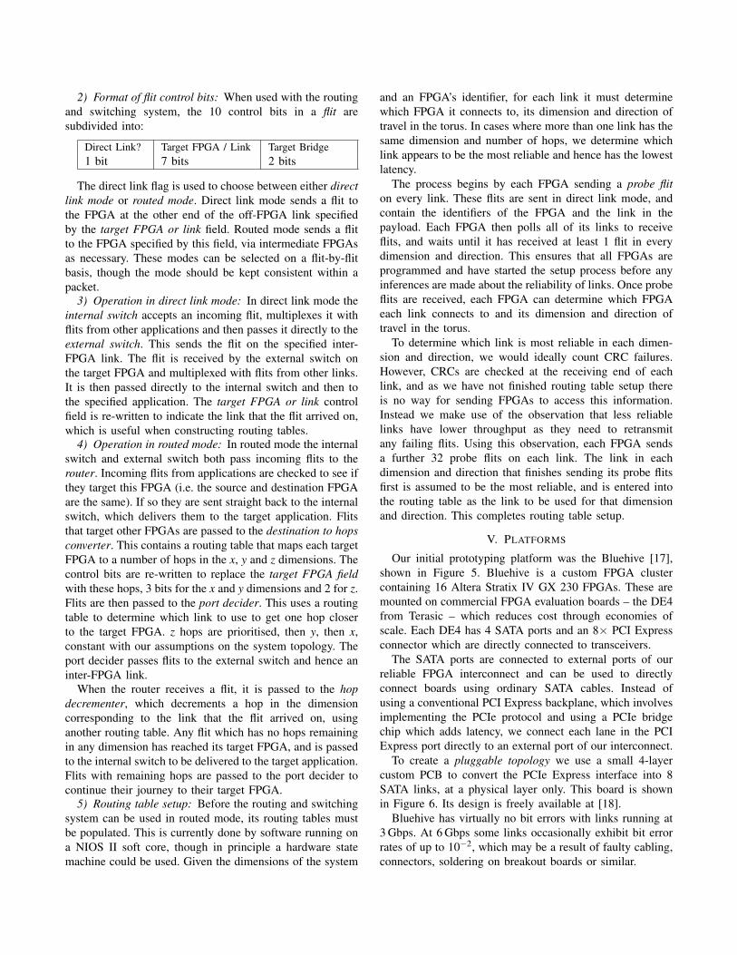
Our initial prototyping platform was the Bluehive [17],shown in Figure 5. Bluehive is a custom FPGA clustercontaining 16 Altera Stratix IV GX 230 FPGAs. These aremounted on commercial FPGA evaluation boards – the DE4from Terasic – which reduces cost through economies ofscale. Each DE4 has 4 SATA ports and an 8× PCI Expressconnector which are directly connected to transceivers.
The SATA ports are connected to external ports of ourreliable FPGA interconnect and can be used to directlyconnect boards using ordinary SATA cables. Instead ofusing a conventional PCI Express backplane, which involvesimplementing the PCIe protocol and using a PCIe bridgechip which adds latency, we connect each lane in the PCIExpress port directly to an external port of our interconnect.
To create a pluggable topology we use a small 4-layercustom PCB to convert the PCIe Express interface into 8SATA links, at a physical layer only. This board is shownin Figure 6. Its design is freely available at [18].
Bluehive has virtually no bit errors with links running at3 Gbps. At 6 Gbps some links occasionally exhibit bit errorrates of up to 10−2, which may be a result of faulty cabling,connectors, soldering on breakout boards or similar.
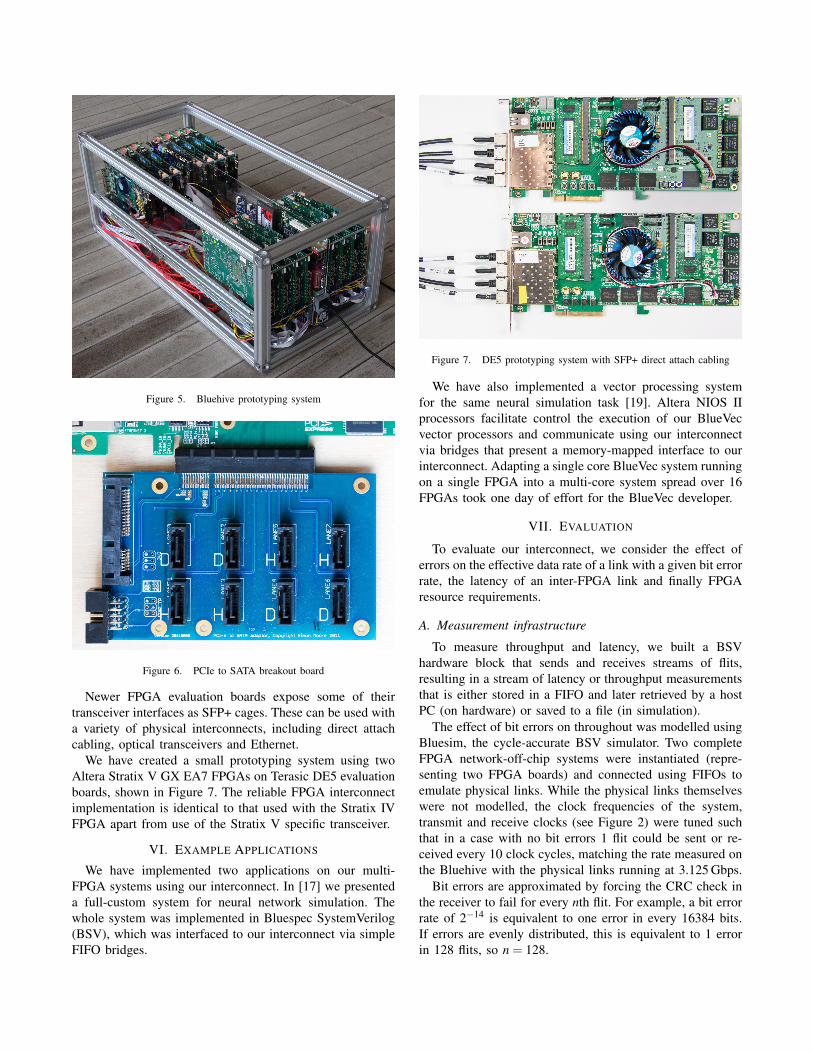
Figure 5. Bluehive prototyping system
Figure 6. PCIe to SATA breakout board
Newer FPGA evaluation boards expose some of theirtransceiver interfaces as SFP+ cages. These can be used witha variety of physical interconnects, including direct attachcabling, optical transceivers and Ethernet.
We have created a small prototyping system using twoAltera Stratix V GX EA7 FPGAs on Terasic DE5 evaluationboards, shown in Figure 7. The reliable FPGA interconnectimplementation is identical to that used with the Stratix IVFPGA apart from use of the Stratix V specific transceiver.
VI. EXAMPLE APPLICATIONS
We have implemented two applications on our multi-FPGA systems using our interconnect. In [17] we presenteda full-custom system for neural network simulation. Thewhole system was implemented in Bluespec SystemVerilog(BSV), which was interfaced to our interconnect via simpleFIFO bridges.
Figure 7. DE5 prototyping system with SFP+ direct attach cabling
We have also implemented a vector processing systemfor the same neural simulation task [19]. Altera NIOS IIprocessors facilitate control the execution of our BlueVecvector processors and communicate using our interconnectvia bridges that present a memory-mapped interface to ourinterconnect. Adapting a single core BlueVec system runningon a single FPGA into a multi-core system spread over 16FPGAs took one day of effort for the BlueVec developer.
VII. EVALUATION
To evaluate our interconnect, we consider the effect oferrors on the effective data rate of a link with a given bit errorrate, the latency of an inter-FPGA link and finally FPGAresource requirements.
A. Measurement infrastructure
To measure throughput and latency, we built a BSVhardware block that sends and receives streams of flits,resulting in a stream of latency or throughput measurementsthat is either stored in a FIFO and later retrieved by a hostPC (on hardware) or saved to a file (in simulation).
The effect of bit errors on throughout was modelled usingBluesim, the cycle-accurate BSV simulator. Two completeFPGA network-off-chip systems were instantiated (repre-senting two FPGA boards) and connected using FIFOs toemulate physical links. While the physical links themselveswere not modelled, the clock frequencies of the system,transmit and receive clocks (see Figure 2) were tuned suchthat in a case with no bit errors 1 flit could be sent or re-ceived every 10 clock cycles, matching the rate measured onthe Bluehive with the physical links running at 3.125 Gbps.
Bit errors are approximated by forcing the CRC check inthe receiver to fail for every nth flit. For example, a bit errorrate of 2−14 is equivalent to one error in every 16384 bits.If errors are evenly distributed, this is equivalent to 1 errorin 128 flits, so n = 128.

0
0.5
1
Thr
ough
put/G
bps
102
104
106
Ret
rans
mits
per
s
10−10 10−9 10−8 10−7 10−6 10−5 10−4 10−3 10−2
100
102
104
106
Bit error rate
CR
Cfa
ilspe
rs
Figure 8. Performance for varying bit error rates (3.125 Gbps link rate)
B. Throughput and Effective data rate
The effect of bit errors on throughput is shown in Figure 8.Effective data rate is derived from throughput by assumingthat each flit that is successfully transmitted carries 64 bitsof useful data. Of particular note is the effective data rateof 1.2 Gbps with a low bit error rate of 10−10. Given that64 bits of payload are carried in a 128 bit flit and that8b10b encoding gives an overhead of 10/8 = 1.25, thisgives an actual data rate on the physical link of 3.0 Gbps,which closely matches the intended physical link data rateof 3.125 Gbps.
It is notable that the data rate for high error rates (10−3 orhigher) is around 40 Mbps. While this is clearly significantlyless than the physical link rate of 3.125 Gbps, this will stillprovide a more than adequate communication link for settingup and monitoring a multi-FPGA cluster, for example toindicate to the operator that some physical links are showinghigh error rates and should be investigated.
C. Latency
The latency of a single inter-FPGA link was measuredusing two Stratix IV GX 230 FPGAs with line rates of3.125 Gbps and 6.250 Gbps (connected using the PCIe–SATA breakout board and SATA cables) and also two StratixV GX EA7 FPGAs with a line rate of 10.0 Gbps (connectedusing SFP+ direct attach cables). Figure 9 shows two typesof measurement for these line rates: unloaded latency usesa single flit at a time on an otherwise unused link and fully
3G 6G 10G 3G 6G 10G
Unloaded Fully loaded
0
200
400
600
800
1000
1200
Lat
ency
/ns
Figure 9. End-to-end latency at different link rates
System Combinational Logic M9KALUT Registers Memory
Reliable Transceiver 1533 (0.8%) 1936 (1.1%) 17 (1.4%)RapidIO Core (1×) 7100 (3.9%) 7600 (4.2%) 51 (4.1%)4× Reliable Transceiver 6132 (3.4%) 7744 (4.2%) 68 (5.5%)RapidIO Core (4×) 9000 (5.0%) 10300 (5.7%) 51 (4.1%)Network-off-Chip Block 28590 (16%) 25248 (14%) 217 (18%)inc NIOS & DDR2 ctl 50667 (28%) 76359 (42%) 337 (27%)
Table IFPGA RESOURCE REQUIREMENTS. FIGURES IN BRACKETS ARE % OF
RESOURCES AVAILABLE ON AN ALTERA STRATIX IV GX 230
loaded latency sends as many flits as possible, as for thethroughout test.
The difference between the unloaded and fully loadedlatencies is primarily a result of 1 to 4 serialisation inthe link layer, which becomes pronounced when transmitbuffers become full. Fully loaded latency is around 1 µs at3.125 Gbps, 600 ns at 6.25 Gbps and 450 ns at 10.0 Gbps,which compares with 1 µs quoted for RapidIO [13] (unclearif unloaded or fully loaded latency) at 10 Gbps line rate.
D. FPGA resources
Table I shows the FPGA resource requirements of ournetwork-off-chip. We measured a single reliable transceiver,a network-off-chip block of 12 reliable transceivers (using 12lanes from a DE4 board), and a full design with network-off-chip, 2× Altera NIOS II processors and 2× DDR2 memorycontrollers plus interfacing logic. The resource requirementsof 1-lane and 4-lane Altera RapidIO cores (taken from [20])are also shown for comparison.
It is clear that our reliable transceiver uses significantlyless resources than the Altera RapidIO core, with 25% ofthe logic usage and 33% of the memory usage. The majorityof the memory usage of the RapidIO core results from itsminimum 8KB transmit buffer and 4KB receive buffer. Thiscompares with the 8-flit and 16-flit transmit and receivebuffers in the reliable transceiver, which use 574 bits and1230 block memory bits respectively, both mapping to threeM9K memory blocks. The remainder of the memory blockusage comes from the clock crossing FIFOs in the link layer.The low buffer sizes that make this lower memory blockutilisation possible are enabled by out short flit size and lowend-to-end latency.

The 4-lane RapidIO core and 4 reliable transceivers arenot directly comparable as the former has a single set ofbuffers and stripes each frame over 4 lanes while the latterare 4 independent channels. However the logic usage of 4reliable transceivers is still lower than that of the 4-laneRapidIO core. Our higher memory block usage indicatesthat using 4 serial links per reliable transceiver will lead topromising future work as memory usage will be reduced. Itcould also eliminate the 1-to-4 serialisation in the link layer,which would significantly reduce latency.
Finally the resource usage of a complete prototypingdesign shows that use of our interconnect leaves ampleFPGA resources for the prototype SoC after communicationand memory interfaces have been instantiated.
VIII. CONCLUSIONS
Our interconnect for multi-FPGA SoC prototyping sys-tems has low latency and is designed to scale to hundreds ofFPGAs. Combined with some custom physical interconnect,it allows us to create multi-FPGA prototyping systems usingcommodity FPGA evaluation boards.
Errors introduced by inter-FPGA links are transparentlydetected and corrected, providing high confidence in thecorrectness of a prototype SoC. Low latency and short dataunits allow us to use much less buffering than comparabletechnologies such as RapidIO, and result in significantlylower latency and FPGA resource utilisation. This is at theexpense of a little bandwidth inefficiency, a trade-off webelieve is appropriate given the high bandwidth of inter-FPGA links.
The combination of transparent error correction, network-on-chip semantics, low latency and low resource usage sim-plifies partitioning of prototype SoCs over multiple FPGAs.
ACKNOWLEDGEMENTS
This work is part of the MRC2 Project that is spon-sored by the Defense Advanced Research Projects Agency(DARPA) and the Air Force Research Laboratory (AFRL),under contract FA8750-11-C-0249. The views, opinions,and/or findings contained in this paper are those of theauthors and should not be interpreted as representing theofficial views or policies, either expressed or implied, ofthe Defense Advanced Research Projects Agency or theDepartment of Defense. We acknowledge additional supportfrom the UK research council, EPSRC, grant EP/G015783/1.We would also like to thank Andrew Moore for his adviceon high-speed communication protocols.
REFERENCES
[1] W. J. Dally and B. Towles, “Route packets, not wires: on-chipinteconnection networks,” in Design Automation, Proceedingsof the 38th Conference on, 2001, pp. 684 – 689.
[2] D. Wang, N. Jerger, and J. Steffan, “DART: A programmablearchitecture for NoC simulation on FPGAs,” in Networks onChip (NoCS), 2011 Fifth IEEE/ACM International Symposiumon, May 2011, pp. 145–152.
[3] P. Wolkotte, P. Holzenspies, and G. J. M. Smit, “Fast, accurateand detailed NoC simulations,” in Networks-on-Chip (NOCS)First International Symposium on, May 2007, pp. 323–332.
[4] Kouadri-Mostefaoui, Abdellah-Medjadji, B. Senouci, andF. Petrot, “Large scale on-chip networks : An accurate multi-FPGA emulation platform,” in Digital System Design Archi-tectures, Methods and Tools, 2008, pp. 3–9.
[5] A. Nejad, M. Martinez, and K. Goossens, “An FPGA bridgepreserving traffic quality of service for on-chip network-basedsystems,” in Design, Automation Test in Europe ConferenceExhibition (DATE), 2011, pp. 1–6.
[6] B. Holden. (2006, November) Latency comparison betweenHyperTransportTM and PCI-ExpressTM in communicationssystems. [Online]. Available: http://www.hypertransport.org/docs/wp/Low Latency Final.pdf
[7] M. Cavalli. (2007, June) Advanced interconnect standardsblend serial and parallel techniques for best performance andscalability. [Online]. Available: http://www.hypertransport.org/docs/wp/Serial vs Parallel.pdf
[8] Intel Corporation. (2012) Thunderbolt technology brief.[Online]. Available: http://www.intel.com/content/dam/doc/technology-brief/thunderbolt-technology-brief.pdf
[9] PCI-SIG, “PCI Express R© base specification revision 3.0,”November 2010.
[10] K. Kong. (2007) PCIe R© as a multiprocessor systeminterconnect. [Online]. Available: http://www.pcisig.com/developers/main/training materials/get document?doc id=8ac11bd327fad024de528e74830b3e6d8b220485
[11] Infiniband TA, “Advantages of Infiniband.” [On-line]. Available: http://www.infinibandta.org/content/pages.php?pg=about us advantages
[12] RapidIO Trade Association. RapidIO interconnectspecification 3.0. [Online]. Available: http://www.rapidio.org/specs/current/2013-oct23.zip
[13] D. Paul, “Low latency servers with RapidIO,”in Open Server Summit, October 2013. [Online].Available: http://www.serverdesignsummit.com/English/Collaterals/Proceedings/2013/20131024 C201 Paul.pdf
[14] T. Bunker and S. Swanson, “Latency-optimized networks forclustering FPGAs,” in Field-Programmable Custom Comput-ing Machines (FCCM), 2013, pp. 129–136.
[15] A. Schmidt, W. Kritikos, R. Sharma, and R. Sass, “AIREN: Anovel integration of on-chip and off-chip FPGA networks,” inField-Programmable Custom Computing Machines (FCCM),2009, pp. 271–274.
[16] P. Watts, S. Moore, and A. Moore, “Energy implicationsof photonic networks with speculative transmission,” Opti-cal Communications and Networking, IEEE/OSA Journal of,vol. 4, no. 6, pp. 503–513, June 2012.
[17] S. W. Moore, P. J. Fox, S. J. T. Marsh, A. T. Markettos,and A. Mujumdar, “Bluehive - a field-programable customcomputing machine for extreme-scale real-time neural net-work simulation,” in Field-Programmable Custom ComputingMachines (FCCM), 2012, pp. 133–140.
[18] “PCIe to SATA breakout board.” [Online]. Available: http://www.cl.cam.ac.uk/research/comparch/opensource/pcie-sata/
[19] M. Naylor, P. Fox, A. Markettos, and S. Moore, “Manag-ing the FPGA memory wall: Custom computing or vectorprocessing?” in Field Programmable Logic and Applications(FPL), Sept 2013, pp. 1–6.
[20] RapidIO MegaCore function user guide. [Online]. Available:http://www.altera.co.uk/literature/ug/ug rapidio.pdf