remote powering platform for implantable sensor …ims.unipv.it/~franco/conferenceproc/362.pdf ·...
TRANSCRIPT

Remote Powering Platform forImplantable Sensor Systems at 2.45 GHz
Onur Kazanc1, Gurkan Yilmaz1, Franco Maloberti2, Catherine Dehollain1
1 RFIC Group, Ecole Polytechnique Federale de Lausanne, Lausanne, Switzerland2 Integrated Microsystems Laboratory, University of Pavia, Pavia, Italy
Abstract— Far-field remotely powered sensor systems enablelong distance operation for low-power sensor systems. In thiswork, we demonstrate a remote powering platform with aminiaturized antenna and remote powering base station oper-ating at 2.45 GHz. The rectenna, which is the energy receivingand conversion element of the sensor system, is designed andmeasured. The measurements for the tag are performed within15 cm distance from the remote powering base station. Therealized gain of the tag antenna is measured as -3.3 dB, whichis 0.5 dB close to the simulations, where simulated realized gainis -2.8 dB.
I. INTRODUCTION
The development of RFIDs gives rise to the implemen-tation of wireless sensor systems for remote monitoringand real-time wireless telemetry. One of the advantages ofthese systems is their battery-free operation which bringsminiaturization. Likewise in RFID, remotely powered sensorsystems utilize ISM frequency bands. For near-field inductivecoupling, the operation frequency is generally selected as13.56 MHz while for far-field electromagnetic coupling, 900MHz and 2.45 GHz frequency bands are chosen [1]. Thewireless sensor systems, which utilize near-field coupling,are mainly focusing on power levels greater than 200 µW [2].The link efficiency of these systems suffers mainly becauseof lateral or angular misalignment between the transmitterand receiver coil [3].
Although, far-field electromagnetic coupling provide lowerenergy density compared to near field coupling, it canprovide a wider coverage of area thanks to the antennaradiation pattern. Therefore, it ensures transmission of powernot limited to the radiator area, and the power delivered isnot affected by the horizontal misalignment of the receivingtag antenna. An application platform of remotely poweredsensor system with electromagnetic coupling is presented inFigure 1. Note that, the beamwidth of the patch antenna cancover a mouse cage where animal mobility is expected.
We aim to design a remote powering platform for im-plantable sensor systems, where the receiving antenna ischosen to operate at 2.45 GHz. The chosen frequency atwhich the antenna exhibits relatively higher gain than 900MHz thanks to its shorter wavelength. Therefore, it enablesimplantable systems with smaller device footprint.
Implanting a device inside the body requires certain spec-ifications to be satisfied in order to guarantee that the bodywill accept the implant. Otherwise, the body exhibits foreign
Tag Antenna
+
Bio-Chip
DATABASE
&
MONITORING
Downlink Uplink
Base
Station+
Reader
Antenna
θθ
Fig. 1. Application platform to measure vital values of laboratory mouse.
body reaction to the implant and it has to be removed.Amongst these specifications, two major goals have beenconsidered in the scope of this study: biocompatibility andbidirectional diffusion barrier. A polymer based packagingis employed in order to protect the implant from the tissuesand vice versa. Therefore, Polydimethylsiloxane (PDMS) isselected as the packaging material since it is shown to bebiocompatible [4]. Moreover, it is preferred as a moisturebarrier material thanks to its hydrophobicity [5].
In this work, we have developed a remote poweringplatform with base station and receiver rectenna, which iscomposed of the antenna and the rectifier, coated with PDMSpolymer. In Section II the rectenna design, which includesrectifier and PDMS coated antenna, is presented. SectionIII describes the base station structure and its components.In Section IV patch antenna design and characterization aregiven. In Section V measurement results of the power link,which is characterized in air, are given. In Section VI resultsof this work are discussed.
II. RECTENNA
A. Determining Non-Linear Rectifier Impedance
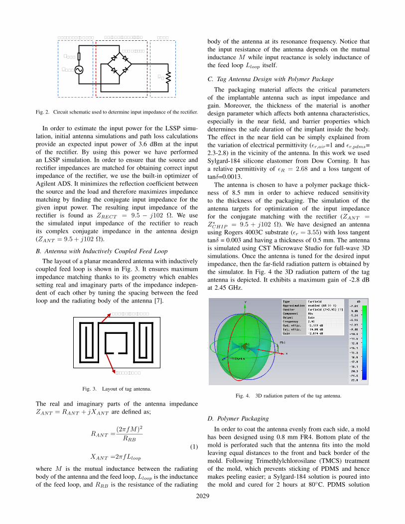
The impedance matching between receiving antenna andthe rectifier determines how much of the incident power onthe antenna is delivered to the rectifier. In order to maximizeimpedance matching, the input impedance of the rectifiershould be determined accurately. Large signal s-parameter(LSSP) simulation permits obtaining the input impedance ofa rectifier when it is matched to its source [6]. The simulationuses the the model of a commercially available diode usedto build a bridge rectifier (Avago HSMS-2828) as shown inFig. 2. The test circuit includes a single tone source at 2.45GHz.
978-1-4244-7929-0/14/$26.00 ©2014 IEEE 2028
ANTENNA MODEL
ZANT
PANT
BRIDGE RECTIFIER LOAD
RL
HSMS-282X
Fig. 2. Circuit schematic used to determine input impedance of the rectifier.
In order to estimate the input power for the LSSP simu-lation, initial antenna simulations and path loss calculationsprovide an expected input power of 3.6 dBm at the inputof the rectifier. By using this power we have performedan LSSP simulation. In order to ensure that the source andrectifier impedances are matched for obtaining correct inputimpedance of the rectifier, we use the built-in optimizer ofAgilent ADS. It minimizes the reflection coefficient betweenthe source and the load and therefore maximizes impedancematching by finding the conjugate input impedance for thegiven input power. The resulting input impedance of therectifier is found as ZRECT = 9.5 − j102 Ω. We usethe simulated input impedance of the rectifier to reachits complex conjugate impedance in the antenna design(ZANT = 9.5 + j102 Ω).
B. Antenna with Inductively Coupled Feed Loop
The layout of a planar meandered antenna with inductivelycoupled feed loop is shown in Fig. 3. It ensures maximumimpedance matching thanks to its geometry which enablessetting real and imaginary parts of the impedance indepen-dent of each other by tuning the spacing between the feedloop and the radiating body of the antenna [7].
RADIATING BODY
FEED LOOP
Fig. 3. Layout of tag antenna.
The real and imaginary parts of the antenna impedanceZANT = RANT + jXANT are defined as;
RANT =(2πfM)2
RRB(1)
XANT =2πfLloop
where M is the mutual inductance between the radiatingbody of the antenna and the feed loop, Lloop is the inductanceof the feed loop, and RRB is the resistance of the radiating
body of the antenna at its resonance frequency. Notice thatthe input resistance of the antenna depends on the mutualinductance M while input reactance is solely inductance ofthe feed loop Lloop itself.
C. Tag Antenna Design with Polymer Package
The packaging material affects the critical parametersof the implantable antenna such as input impedance andgain. Moreover, the thickness of the material is anotherdesign parameter which affects both antenna characteristics,especially in the near field, and barrier properties whichdetermines the safe duration of the implant inside the body.The effect in the near field can be simply explained fromthe variation of electrical permittivity (εr,air=1 and εr,pdms=2.3-2.8) in the vicinity of the antenna. In this work we usedSylgard-184 silicone elastomer from Dow Corning. It hasa relative permittivity of εR = 2.68 and a loss tangent oftanδ=0.0013.
The antenna is chosen to have a polymer package thick-ness of 8.5 mm in order to achieve reduced sensitivityto the thickness of the packaging. The simulation of theantenna targets for optimization of the input impedancefor the conjugate matching with the rectifier (ZANT =Z∗CHIP = 9.5 + j102 Ω). We have designed an antenna
using Rogers 4003C substrate (εr = 3.55) with loss tangenttanδ = 0.003 and having a thickness of 0.5 mm. The antennais simulated using CST Microwave Studio for full-wave 3Dsimulations. Once the antenna is tuned for the desired inputimpedance, then the far-field radiation pattern is obtained bythe simulator. In Fig. 4 the 3D radiation pattern of the tagantenna is depicted. It exhibits a maximum gain of -2.8 dBat 2.45 GHz.
Fig. 4. 3D radiation pattern of the tag antenna.
D. Polymer Packaging
In order to coat the antenna evenly from each side, a moldhas been designed using 0.8 mm FR4. Bottom plate of themold is perforated such that the antenna fits into the moldleaving equal distances to the front and back border of themold. Following Trimethlylchlorosilane (TMCS) treatmentof the mold, which prevents sticking of PDMS and hencemakes peeling easier; a Sylgard-184 solution is poured intothe mold and cured for 2 hours at 80C. PDMS solution
2029

is composed of base agent and curing agent at a 10:1 ratio,respectively. Fig. 5 illustrates the alignment of the antenna tothe molding structure. As previously mentioned the thicknessof the antenna with PDMS coating is 8.5 mm. Therefore, thefront and back thickness of PDMS (a) is 4 mm, sidewallthickness (b) is 1 mm, and the thickness of the antennasubstrate (c) is 0.5 mm.
aa
b
a: front & back thickness
b: side thickness
c: antenna PCB thickness
c
CHIP
Fig. 5. Front view of the antenna and top view of the bottom plate of themold.
In Fig. 6 the antenna with the mounted rectifier, whichis coated with PDMS is shown. The final volume of theimplantable rectenna is 18x11x8.5 mm3. At the tail of thepackage the RC output load and terminals to measure DCoutput voltage of the rectifier are highlighted.
Fig. 6. Fabricated antenna with PDMS coating.
III. REMOTE POWERING BASE STATION
The block diagram of the remote powering base station isshown in Fig. 7. The signal chain consists of a PLL frequencysynthesizer (Analog Devices ADF4360-0) for carrier fre-quency generation and a power amplifier (RFMD 2172). Thepower amplifier is utilized to increase the output power ofthe base station sufficient for remote powering applications.The power amplifier, which is driven by the PLL, has 1 dBcompression point at 23 dBm. The signal chain is completedby a transmitting patch antenna, where the output power ofthe power amplifier absorbed and radiated.
The PLL is programmable through the SPI port by usingTexas Instruments MSP430 microcontroller. We have mea-
μC
MSP430
PA
POWER AMP
Gain PATCH
ANTENNA
SPI Control
PLL
AD 4360-0
RFMD2172
Fig. 7. Block diagram of remote powering base station for 2.45 GHz.
sured the output power of the base station while sweepingthe output power of the PLL through the programmable SPIinterface using the microcontroller. The output power of theremote powering base station ranges from +14.2 dBm to +23dBm.
IV. PATCH ANTENNA
Once the tag is fabricated, it is pre-measured with awideband antenna, in this case a helical antenna, in order tofind its resonance frequency before further characterization.The tag antenna, which is connected with rectifier and theoutput load, is measured and resonates at 2441 MHz. Next,the design and fabrication of patch antenna for 2441 MHz isperformed once resonance of the tag antenna is measured.
The antenna of the remote powering base station is chosenas a patch antenna. The angle of emission is directed towardsone direction and exhibits a beamwidth around 90. Thisenables the antenna to be used for the proposed monitoringapplication. The implemented patch antenna of the RFIDreader is based on an inset-fed patch antenna [8]. Theantenna, which is designed for 2441 MHz, is built on aRogers 5880 Duroid (εr=2.2) substrate with a low tangentloss (tanδ ≈ 0.005). The 3D full-wave simulation of thepatch antenna is performed using CST Microwave Studio.The radiation pattern of the patch antenna is measured inan anechoic chamber. The simulated and measured radiationpattern is depicted in Fig. 8. The maximum gain of the patchantenna is measured as 7.2 dB while simulated maximumgain is 7.4 dB.
−22.2
−22.2
−14.4
−14.4
−6.6
−6.6
1.2
1.2
9 dB
9 dB
90o
60o
30o0o
−30o
−60o
−90o
−120o
−150o
180o150o
120o
SimMeas
Fig. 8. Simulated and measured radiation pattern of the inset-fed patchantenna.
2030

The fabricated patch antenna is measured with a vectornetwork analyzer (VNA) in order to determine input reflec-tion coefficient (S11). The input reflection coefficient of theantenna is measured as -18 dB at 2441 MHz.
V. MEASUREMENT RESULTS
We derive the realized gain GRX(R) of the tag antennaindirectly by simulating and measuring rectenna while know-ing the path loss, output power of the remote powering basestation, and the patch antenna gain. The measurement schemeof the rectenna is depicted in Fig. 9. The transmitting andreceiving antennas are placed d =15 cm apart from eachother in order to operate in far-field region.
POWER
RECTIFIER
ZC
TA
G A
NT
EN
NA
d
RL
BASE
STATION
+
-VRECT
Fig. 9. Measurement setup for rectenna characterization.
Fig. 10. Remote powering base station with patch antenna.
The PEIRP of the remote powering base station shownin Fig. 10 is set to 30.2 dBm (≈1W). Then we calculatethe path loss for 15 cm separation, which is found as 23.8dB. Subtracting this from the PEIRP , the expected inputpower for an isotropic radiator is 6.4 dBm and the expectedpower for our tag antenna, which has a simulated gain of-2.8 dB, is 3.6 dBm. Corresponding simulated efficiency ofthe rectifier for the given input power is found as 10.9%by using harmonic balance simulator. The realized gain ofthe tag antenna GRX(R) can be written by modified Friisequation,
GRX(R) =POUT
PTX ·GTX ·[λ
4πd
]2 · η (2)
where the efficiency of the rectifier (η) is accounted for.By measuring the rectenna with an output load of RL=30 kΩ we obtained a DC output voltage VRECT equalto 2.6 V, whereas the simulated output voltage is 2.74 Vassuming ideal matching. Measured and simulated outputpowers are 250 µW and 225 µW, respectively. Using (2) we
calculate the realized gain GRX(R) of the tag antenna whileassuming the rectifier efficiency is kept constant at 10.9 %.We calculated the realized gain of the tag antenna as -3.3dB. Based on these results, we find the difference betweenthe simulations and the measured realized gain GRX(R) as0.5 dB. This difference can be explained by the nonidealimpedance matching and efficiency variation in the rectifier.Nevertheless, the proposed method enables characterizationof the remote powering link in a simple and accurate manner.Note that the measurement of the rectenna is performed in airand output power level is above 200 µW. In order to verifyin-vivo performance, antenna is needed to be redesigned forin-vivo environment for realistic surroundings.
VI. CONCLUSION
In this work we have presented a remote powering plat-form targeting implantable sensor system applications at 2.45GHz. The work covers the design of the remote poweringbase station and the receiving tag antenna with the rectifier.The tag antenna is coated with polymer and the employedmolding method is described. Measurements are performedwith the rectenna, which is composed of the designed tagantenna and a commercial rectifier in order to achievereal application measurements. The remote powering linkis characterized from remote powering base station to theoutput of the rectifier. The measured antenna performs arealized gain of -3.3 dB while simulated realized gain is-2.8 dB, showing that measurements and simulations agreewell.
ACKNOWLEDGMENT
This work is funded by Nano-Tera initiative of SwissNational Funding (SNF) project entitled “I-Ironic” and bySNF project entitled “Epilepsy in-vivo”.
REFERENCES
[1] K. Finkenzeller, “RFID Handbook: Fundamentals and Applications inContactless Snart Cards and Identification", 2nd Edition, John Wiley& Sons, NY, USA, 2003
[2] N. Chaimanonart, D. J. Young, “An Adaptively RF-Powered WirelessBatteryless In Vivo EKG and Core Body Temperature Sensing Mi-crosystem for Untethered Genetically Engineered Mice Real-Time Mon-itoring”, 6th International Conference on Network Sensing Systems(INSS), pp. 1-6, June 2009
[3] E.G. Kilinc, C. Dehollain; F. Maloberti, “Design and optimization ofinductive power transmission for implantable sensor system”, XIth In-ternational Workshop on Symbolic and Numerical Methods, Modelingand Applications to Circuit Design (SM2ACD), 2010, pp.1-5, 4-6 Oct.2010
[4] M. Belanger, Y. Marois, “Hemocompatibility, Biocompatibility, In-flammatory and In-Vivo Studies of Primary Reference Materials Low-Density Polyethylene and Polydimethylsiloxane: A review.", Journal ofBiomedical Materials Research, vol.58, no.5, pp.467-477, Jul. 2001
[5] C. Lu, Y. Sun, S. J. Harley, E.A. Glascoe, “Modeling Gas Transportand Reactions in Polydimethysiloxane", Proceedings in TOUGH Sym-posium, pp.1-8, Sep. 2012
[6] O. Kazanc, F. Maloberti, C. Dehollain, “Simulation oriented rectennadesign methodology for remote powering of wireless sensor systems",IEEE International Symposium on Circuits and Systems (ISCAS),pp.2877,2880, May 2012
[7] H. W. Son and C. S. Pyo, “Design of RFID Tag Antennas Using anInductively Coupled Feed", Electronics Letters, vol.41, no.8, pp.994-996, Sep. 2005
[8] C. A. Balanis, “Antenna Theory: Analysis and Design”, Second Edi-tion, Wiley-Interscience, 2005
2031