repair and re-balling stencils 1.5 for smd components · repair and re-balling stencils for smd...
TRANSCRIPT
1.5Repair and Re-balling stencils for SMD components
Application
With the introduction of SMD-technology and the constant drive toward miniaturization of components, new procedures and repair processes are constantly being developed in order to provide reliable repair materials and safe repair procedures. Despite the low failure rates of many of the new integrated circuits, the high cost of these devices, and the subse-quent cost of the populated PCB require a reliable repair solution. It is very rare for a new product to achieve a first-pass yield of 100 %. Increased component geometries and component leads, particularly with area array components, create the need for tighter tolerances and accuracy from rework systems and rework stencils. Therefore, a fool-proof repair process is necessary. Decreased spacing of component leads has also gene-rated additional challenges for repair processes and repair stencils. With the high demand on quality and reliability, component repair is getting more complex and time consuming.For over 10 years, LaserJob has been producing high-accuracy laser cut stencils for a variety of rework and repair stations.
Manufacturing in the laser cut and laser welding process
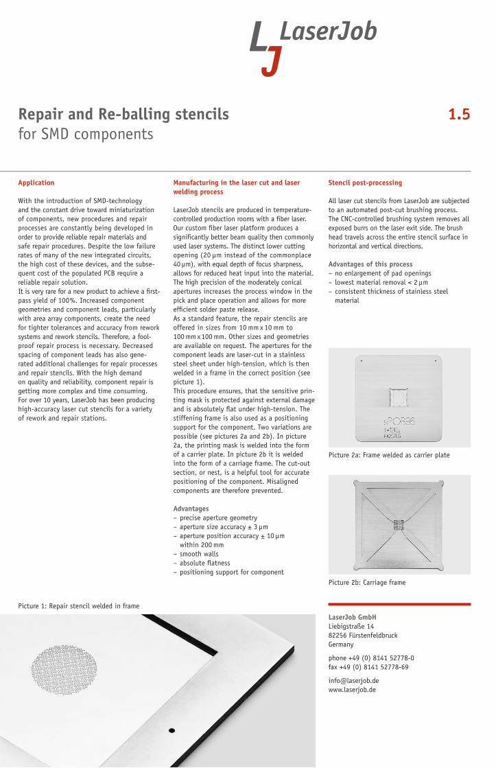
LaserJob stencils are produced in temperature-controlled production rooms with a fiber laser. Our custom fiber laser platform produces a significantly better beam quality then commonly used laser systems. The distinct lower cutting opening (20 µm instead of the commonplace 40 µm), with equal depth of focus sharpness, allows for reduced heat input into the material. The high precision of the moderately conical apertures increases the process window in the pick and place operation and allows for more efficient solder paste release.As a standard feature, the repair stencils are offered in sizes from 10 mm x 10 mm to 100 mm x 100 mm. Other sizes and geometries are available on request. The apertures for the component leads are laser-cut in a stainless steel sheet under high-tension, which is then welded in a frame in the correct position (see picture 1). This procedure ensures, that the sensitive prin-ting mask is protected against external damage and is absolutely flat under high-tension. The stiffening frame is also used as a positioning support for the component. Two variations are possible (see pictures 2a and 2b). In picture 2a, the printing mask is welded into the form of a carrier plate. In picture 2b it is welded into the form of a carriage frame. The cut-out section, or nest, is a helpful tool for accurate positioning of the component. Misaligned components are therefore prevented.
Advantages – precise aperture geometry– aperture size accuracy ± 3 µm– aperture position accuracy ± 10 µm within 200 mm– smooth walls– absolute flatness– positioning support for component
Circlip Toothed washer
Stencil post-processing
All laser cut stencils from LaserJob are subjected to an automated post-cut brushing process. The CNC-controlled brushing system removes all exposed burrs on the laser exit side. The brush head travels across the entire stencil surface in horizontal and vertical directions.
Advantages of this process– no enlargement of pad openings– lowest material removal < 2 µm– consistent thickness of stainless steel material
Picture 1: Repair stencil welded in frame
Picture 2a: Frame welded as carrier plate
Picture 2b: Carriage frame
LaserJob GmbHLiebigstraße 1482256 FürstenfeldbruckGermany
phone +49 (0) 8141 52778-0fax +49 (0) 8141 52778-69
Repair and Re-balling stencils for SMD components
Simple printing stencil
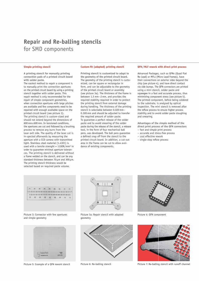
A printing stencil for manually printing connection pads of a printed circuit board with solder paste.The easiest method to repair a component is to manually print the connection apertures on the printed circuit board by using a printing stencil together with solder paste. This repair method is only recommended for the repair of simple component geometries, when connection apertures with large pitches are available and few components need to be repaired with enough available space on the printed circuit board (see picture 3). The printing stencil is custom-sized and should not extend beyond the dimensions of 600 mm x 600 mm. In tensioned conditions, the apertures are cut and followed by a brushing process to remove any burrs from the laser exit side. The quality of the laser cut is in-spected afterwards by measuring theaperture with a CCD camera with transmittedlight. Stainless steel material (1.4301) is used with a tensile strenght > 1100N / mm² in order to guarantee minimal aperture toleran-ces. The printing stencil is delivered without a frame welded on the stencil, and can be any standard thickness between 70 µm and 300 µm. The printing stencil thickness would be selected based on required paste volume.
QFN / MLF rework with direct print process
Advanced Packages, such as QFNs (Quad Flat No Lead) or MFLs (Micro Lead Frames), have their connections on exterior sides beyond the chip (see picture 4), and have direct contact via side bumps. The QFN-connectors are printed using a mini stencil, solder paste and squeegee in a fast and accurate process, thus minimizing component stress (see picture 5). The printed component, before being soldered to the substrate, is analysed by optical inspection. The mini stencil is removed after the refl ow process to ensure higher process stability and to avoid solder paste sloughing and smearing.
Advantages of the simple method of the direct print process of the QFN connectors – fast and simple print process– accurate and stress-free process– cost effective rework– single-step refl ow process
Custom-fi t (adapted) printing stencil
Printing stencil is customized to adapt to the geometry of the printed circuit board.The geometry of the printing stencil is custo-mized, can be square or rectangular in form, and can be adjustable to the geometry of the printed circuit board or assembly (see picture 3a). The thickness of the frame is between 1,5 mm –2 mm, and provides the required stability required in order to protect the printing stencil from external damage during handling. The thickness of the printing stencil is selectable between 0.020 mm–0.300 mm and should be adjusted to transfer the required amount of solder paste. To guarantee a perfect release of the solder paste and to avoid smearing of the solder paste during the release of the stencil, a release tool, in the form of four mechanical ball pens, was developed. The ball pens guarantee a defi ned snap off from the stencil to the printed circuit board. In addition, a cut-out area in the frame can be cut to allow avoi-dance of existing components.
Picture 3: Connector with few apertures and simple geometry
Picture 4: QFN component
Picture 5: Example of a QFN rework stencil
Picture 3a: Repair stencil with adapted geometry
Picture 6: Re-balling stencil Picture 7: Re-balling stencil with runoff channel

Re-balling of BGAs or CSPs with a re-soldering process
The repair or re-soldering of BGAs is a common process in the electronic production. The con-nections of the de-soldered BGAs or CSPs arequite often damaged to the point that they are no longer able to be re-soldered to the prin-ted circuit board. After the residual solder is removed from the land area, a fl ux pen is used to wet the BGA-connections. With the aid of a suitable mask with the corresponding pitch of the BGA balls, the balls are distri-buted over the mask (see picture 6). The excess balls, which have not dropped into the stencil apertures, are diverted back into the container utilizing a runoff channel (see picture 7). With the recommended refl ow process, the balls on the BGA connections are refl owed.
Repair of BGA with a solder paste print process on the PCB
It is also possible to print solder paste direct onto the printed circuit board (PCB) with the support of a stencil in lieu of the re-balling process. After de-soldering the component, the residual solder is removed with an extractor or with solder braid. Solder paste is applied, via a stencil, onto the PCB (see picture 8). Afterwards, the component is placed onto the PCB and refl owed.
Weld seams
Repair stencil
Design proposal for the print process of QFN-components
For connecting apertures of all 4 sides of the package, we recommend the use of a pitch of 0,4 mm, a stencil opening of 0,200 mm x 1,20 mm, and a stencil thickness of 120 µm. This produces an area ratio of 0,86 and a uniform reduction of the stencil opening of –50 µm. In the printing process for a Thermal Die Pad Area, a stencil opening reduction 50–80 % (from the PCB connection pad size) is recommended. This procedure prevents a "fl oating" or "tipping" of the component. In addition, a reduced amount of solder paste minimizes the "voiding" effect of the Thermal Die Pad Area. The printing processes of the Thermal Die Pad Area are realized in three different variations. An example of a VQFN-64-3 component with a Thermal Die Pad Area of 7,10 mm x 7,10 mm is illustrated.
Variation 1: round shape of Thermal Die Pad Area (Stencil thickness: 100 µm)Stencil opening: circular pads: 390 µm x 220 µm (–10 µm reduction in length and width), pitch 0.5 mmStencil opening for Thermal Die Pad Area: Ø 950 µm, pitch 1.65 mm. This represents a 78 % reduction in the size of the thermal apertures.
Variation 2: square shape of Thermal Die Pad Area (Stencil thickness: 100 µm)Stencil opening: circular pads: 390 µm x 220 µm (–10 µm reduction in length and width), pitch 0,5 mmStencil opening for Thermal Die Pad Area: 4 x 1,88 mm x 1,88 mm, mini-tab: 0.5 mm. This represents a 70 % reduction in the size of the thermal apertures.
Variation 3: wing shape of Thermal Die Pads Area (Stencil thickness: 100 µm)Stencil opening: circular pads: 390 µm x 220 µm (–10 µm reduction in length and width), pitch 0.5 mmStencil opening for Thermal Die Pad Area: 4 x 0,68 mm x 1.2 mm x 1.58 mm, mini-tab: 0.5 mm–0.110 mm. This represents a 75 % reduction in the size of the thermal apertures.
Picture 8: Direct solder paste printing process on the PCB (company Finetech)
Quality control
Quality assurance is paramount at LaserJob. Effective quality control starts with incoming inspection of stainless steel sheets and stencil frames. A thickness measurement instrument controls every stainless steel sheet with an accuracy of ±0.5 µm. Pad size and pad geome-tries are inspected immediately after the laser cutting process. The aperture shape is measured, via CCD-camera with transmitted light, to a precision of 1.0 µm. The tolerances of the laser cut opening are illustrated in picture 9.
Picture 9: Tolerances of a laser cut opening
1 / 2 stencil thickness
x = reference value
x = a + b 2
squeegee side
assembly side
± 3 µm
± 3 µm
bxa
b = value measured by transmitted lighta = value measured by refl ected lighta = b + ≤ 12 µma – b = ≤ 12 µmb = x – ≤ 6 µma = x + ≤ 6 µm

www.laserjob.deService
LaserJob offers a full range of consulting services for layout and design. Our team generates, from your CAD-CAM data, automatic cutting in-structions for the laser. Our highly focused laser systems cut with high positioning accu-racy the apertures.
We offer additional– scaling apertures up and down– changing aperture design, e.g. home plates and rounding sharp corners– optimizing apertures (anti tombstone design)– rotating or mirroring of the whole design or sub-areas– control of aspect and area ratios– generation of stencils with multiple panels– generating layouts from existing PCBs– generating stencil layouts for adhesive applications – customer-specific storage for used frames. The frames will be cleaned, re-strung and provided for new orders. Your actual inventory is always retrievable.– data storage– test certificates (as well as customer’s specifications)– data for solder paste inspection systems– Data Matrix Code– measuring of printed circuit boards– production of stencils from provided PCBs, stencils, or films
Fulfillment
The stainless steel material, which is utilized for the stencils, has an optimal hardness and tensile strength. Only stainless steel sheets with a nominal thickness variance are utilized.
MaterialStainless steel: 1.4301Hardness (Hv): min 370Tensile strength (N / mm²): > 1100Thickness of stainless steel sheet: ± 3 %
Dimensions of stainless steel materialsRepair stencils in metal sheet thicknesses of (µm):20, 30, 40, 50, 60, 70, 80, 90, 100, 120, 130, 140, 150, 180, 200, 250, 300, 400Maximum thickness of metal sheet: 2 mmMaximum machine surface: 800 mm x 600 mm
Variances– NanoWork®-stencil – PatchWork®-stencil (Step stencil)– 3D PatchWork®-stencil – combination PatchWork®-stencil with NanoWork®-coating– stencil in screen printing frame glued over stainless steel mesh– in tensioning system LJ 745– in Quattroflex tensioning system – in VectorGuard® tensioning system – in Alpha Tetra/Micromount/Vector tensioning system – in Zelflex tensioning system – in Stencilman tensioning system – in customer-specific tensioning system
Shipping conditions
Shipping timeStandard shipment time ex works is3 work daysOrder entry before 5 p.m. (= first work day)
Common carrier: TNT, UPS, DHL, GO, FedEX (any shipping service) as well as direct shipments with courier delivery with partner companies.
PackagingAll LaserJob stencils are shipped in reusable packaging. To avoid damage of stencils, proven packaging materials are used. We deliver stencils in specialty packaging as well as per customer request.
Order processFor complete processing, we need the drawing of the component with tolerances. We can read drawings in DXF-format or Gerber files. To guarantee fast handling of your order, send the purchase order via
– e-Mail: [email protected]– fax: +49 (0) 8141 52778-60– post
Please send the gerber files for the stencils via e-mail to [email protected]
We are ISO 9001:2015 certified
LaserJob data sheets1.0 SMD stencil1.1 NanoWork®-stencil1.2 PatchWork®-stencil1.3 Tensioning system LJ 745 1.4 Frames and tensioning system1.5 Repair and Re-balling stencil 1.6 Wafer bumping-stencil1.7 LTCC Via fill-stencil2.0 Laser Material Processing
Auch in Deutsch erhältlich.
As of 03/ 2017© LaserJob GmbH