repetitive avalanche and dv/dt rated*njsemi.com/datasheets/irf720 - irf723.pdf · repetitive...
TRANSCRIPT
, Line.
20 STERN AVE.SPRINGFIELD, NEW JERSEY 07081U.S.A.
TELEPHONE: (973) 376-2922(212)227-6005
FAX: (973) 376-8960
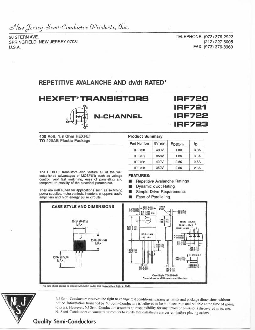
REPETITIVE AVALANCHE AND dv/dt RATED*
IM-CHAIMNEL
400 Volt, 1.8 Ohm HEXFETTO-220AB Plastic Package
Product Summary
The HEXFET transistors also feature all of the wellestablished advantages of MOSFETs such as voltagecontrol, very fast switching, ease of paralleling andtemperature stability of the electrical parameters.
They are well suited for applications such as switchingpower supplies, motor controls, inverters, choppers, audioamplifiers and high energy pulse circuits.
Part Number
IRF720
IRF721
IRF722
(RF723 '
BVDSS
400V
350V
400V
350V
RDS(on)
1.8Q
1.80
2.50
2.5(1
"D3.3A
3.3A
2.8A
2.8A
FEATURES:• Repetitive Avalanche Ratings• Dynamic dv/dt Rating• Simple Drive Requirements• Ease of Paralleling
CASE STYLE AND DIMENSIONS
10.54 (0.415)
ri•f13.97 (0.550)
MAX.
1
MAX.
~~T -1 15.09 (0.594)
MAX.i
•fTIiI
• r•
2.1! 10 11312(210.103)
t T1 }
UM-
139!13.4!
OS941
_ I054I0.4ISI _.10.29 (0 4dil "
3.71 10.1491 „,.3 54 10.1391 u"
IT0
1.1— i
1SSO)
osioi
|
J
(045)MIN.
j-*—
I
TEKM4-0(I»IN |
648I025SJfiTioTfl
^
3MIHISSI3 44 |S HOI
i
||
V-
I2ZI0041)
TERM3 -SOURCE
TERM 2 - D » A I N
TERM 1 - G A T E , \ \/ (0.160) I Am *
43ZfO.UO) 1
2.79(0.110)?»(OMQ) 1
IBI*83(
\
ll\ \
210)
'190)
^SECTION X-X
SI!SrH0939(
Co* Styl. TO-220ABOimeniioni in Millimeters and llnchn)
037}
•This data sheet applies to product with batch codes that begin with a digit, a. 2A3B
NJ Semi-Conductors reserves the right to change test conditions, parameter limits and package dimensions withoutnotice. Information furnished h> NJ Semi-Conductors is believed to be both accurate and reliable at the time of goingto press. However, NJ Semi-Conductors assumes no responsibility for any errors or omissions discovered in its use.N.I Semi-Conductors encourages customers to verify that datasheets are current before placing orders.
Quality Semi-Conductors

IRF720, IRF721, IRF722, IRF723 Devices
Absolute Maximum RatingsParameter
ID ® TC ™ 25°C Continuous Drain Current
ID ® TC " 100°C Continuous Drain Current
IOM Pulsed Drain Current (0
PO @ ̂ C = 25°C Max. Fbwer Dissipation
Linear Derating Factor
VQS Gate-to-Source Voltage
EAS Single Pulsa Avalanche Energy <S>
I AR Avalanche Current ©(Repetitive or Non-Repetitive)
EAR Repetitive Avalanche Energy CD
Jv/ctt - Peak Diode Recovery rfv/dt 0)
Tj Operating JunctionTSTG Storage Temperature Range
Lead Temperature
IRF720, IRF721
3.3
2.1
13
IRF722. IRR23
2.8
. . 1.8 . - -
11
60 '
0.40
±20
190{See Fig. 14)
3.3(See EAR)
5.0(See IAR)
4.0(See Rg. 17)
-66 to 150
300 (0.063 In. 0.6mm) from case lor 10s)
Units
A
A
A
W
VWK®
V
mj
A
mj
Vfns
°C
°C
Electrical Characteristics @ T, = 25°C (Unless Otherwise Specified)Parameter
BVoss Drain-to-Source Breakdown voltage
Fine/nut Static Drain-to-SourceOn-State Resistance 9)
'Dion) On-State Drain Current ®
VGS(th) Gate Threshold Voltage
gfs Forward Transconductance ®
'DSS Ze[0 Gate voltagu Drain Current
1GSS Gate-to-Source Leakage Forward
IQSS Gate-to-Source Leakage Reverse
Qg Total Gate Charge
QgS Gate-to-Source Charge
Qgd Gate-to-Draln ("Mlller'1 Charge
'dtonl Turn-On Delay Time
t, Rise Time
'd(off) Turn-Off Delay Time
t| Fall Time
Lrj Internal Drain Inductance
Lg Internal Source Inductance
Cjgg Input Capacitance
COS3 Output Capacitance
Crss Reverse Transfer Capacitance
Type
IRF720IRF722
IRF721IRF723
IRF720IRF72I
IRF722IRF723
IRR20IRR21
IRF722IRF723
ALL
ALL
ALL
ALL
ALL
ALL
ALL
ALL
ALL
ALL
ALL
ALL
ALL
ALL
ALL
ALL
Win.
400
350
-
-
3.3
2.B
2.0
1.8
-
—
-
-
-
-
-
-
-
-
-
-
-
-
Typ.
-
1.6
1.8
-
-
2.7
-
—
-
-
13
2.2
7.2
10
14
30
13
4.5
7.6
350
64
8.1
Max.
-
1.8
2.5
-
4.0
-
250
1000
500
-500
20
3.3
11
15
21
45
20
-
- -
-
Units
V
0
A
V
SID)
liA
nA
nA
nC
nC
nC
ns
ns
ns
ns
nH
nH
PF
pF
pF
Test Conditions
vGS - ov, iD - 250 ^A
vGS - iov, iD = I.SA
VDS > bton) x "DSIon) Max.VGS = 10V
VDS = VGS. 'D - ZS<VAIDS = i.8A, VDS a wvVOS = Max. Rating, VQS = OV
Vrjs ~ 0.8 X Max RatingVCS - OV, Tj - 125°C
VQS = 2°V
VGS = -20V
VGS - 1"v. ID - 3 3AVQS * 0.8 x Max. RatingSee Rg. 16(Independent of operating temperature)
vDD = 2oov, iD - 3.3A, RG = ienRD = senSes Rg. 15
(Independent of operating temperature)
Measured from the drain Modified MOSFET symbollead, 6mm (0.25 in.) from showing the internalpackage to center of die. inductances. ~ — It
Measured from the source / itl ilead, 6mm 10.25 in.) from i , IT...package to source bonding \ KT
VGS = "« VDS - 25V
f = 1.0 MHi
See Fig. 10
IRF720, IRF721, IRF722, IRF723 Devices
Source-Drain Diode Ratings and CharacteristicsParameter
Ic Continuous Source Current(Body Diodel
ISM Pulsed Source Current(Body Diodel (D
Vsp Diode Forward Vfaltage ®
t,, Reverse Recovery Time
OpR Reverse Recovery Charge
ton Forward Turn-On Time
Type
ALL
AU
ALL
ALL
ALL
ALL
Mm.
-
~
-
120
0.64
Typ,
-
~
-
270
1.4
Max.
3.3
13
1.6
600
3.0
Units
A
A
V
ns
fC
Test Conditions
Modified MOSFET symbol showing the integre)Reverse p-n junction icctifier. -~- — 3t
Tj = 25°C, ls = 3.3A. VGS = 0V
Tj - 2S°C, IF - 3.3A. <i\Ul = 100 A/,a
Intrinsic turn-on time is negligible. Turn-on speed is substantially controlled by LS t LQ.
Thermal ResistanceRtnJC JuncUon-to-Csse
RlhCS Case-to-SInk
RthjA Junction-to-Ambient
ALL
ALL
ALL
-
-
-
-
0.50
-
2.5
-
30
K/W®
IOW®
KW®
Mounting surface fiat, smooth, and greased
Typical socket mount
Typical SPICE Computer Model Parameters (For More Information See Application Note AN-975)
Device
ALL
Level.SPICE
MOSFETModel
3
W(m),ChannelWidth
0.279
Llpm),ChannelLength
1.2
Theta (1M,Mobility
Modulation
0.30
UO (CM2/V-S),SurfaceMobility
450
VTOCV),ThresholdVoltage
4.00
R1 (D),Drain
Resistance
1.4
R2(Q),Source
Resistance
0.02
RG ID).Gate
Resistance
1.5
CGSO (pfl.Gate-
SourceCapacitance
770
CGD(F)Gate-Drain
Capacitance
ca
E1 (V),Voltage Dependent
Voltage Source
2 + 0.995 VDQ
LO InH),Drain
Inductance
4.5
LS(nH),Source
Inductance
7.6
LGInH),Gate
Inductance
7.6
HIM,Diode
SaturationCurrent
3.6 x 10'13
RSIO),DiodeBulk
Resistance
0.026
C8 = 1500 pf + 1.8 x 10⁻²² (VQt;)48
0> Repetitive Rating; Pulse width limited bymaximum function temperature (see figure 5)Refer to current HEXFET reliability report
® 0 VDD • BOV. Starting Tj - 26°C,L - 31 mH.RQ = 250,Peak IL - 3.3A.
01 ISD s 3.3A, d/dt £ 66A/M3,VOD =i 8VDSS, Tj i 160°CSuggested RQ - 180
® Pulse width s 300 ia; Duty Cycle s 2%
K/W = °C/WW/K - W/°C
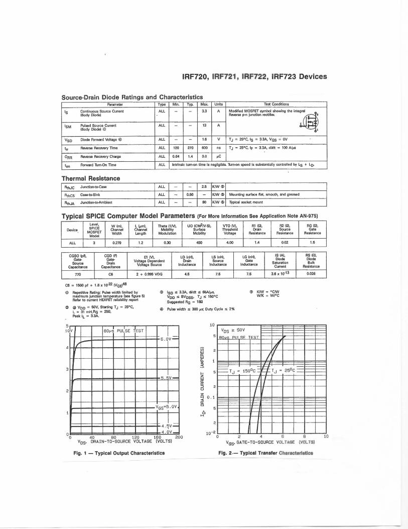
80HS PULSE TEST
6.0V—i
V6S=5.0VJ
•4.5V-A nv
0 40 80 ISO 160 200VDS. DRAIN-TO-SQUHCE VOLTAGE (VOLTS)
Fig. 1 — Typical Output Characteristics
s•^
0.1
10-2I
Vnc
80pl
z E
. PUL
T , =
0V
si-
isc
j)
ESJ
°c
y//g/ // i' /' /1
t
/(J4' /i1\
=
i
j/a
[
r i -
i
^
250(
t 1(Vss. GATE-TO-SOURCE VOLTAGE (VOLTS)
Fig. 2— Typical Transfer Characteristics