research article applying the analog configurability test
TRANSCRIPT

Research ArticleApplying the Analog Configurability Test Approach in a WirelessSensor Network Application
Agustín Laprovitta,1 Gabriela Peretti,2 and Eduardo Romero2
1 Communication Laboratory, Engineering Faculty, Universidad Catolica de Cordoba, Avenida Armada Argentina 3555,5017 Cordoba, Argentina
2Mechatronics Research Group, Facultad Regional Villa Marıa, Universidad Tecnologica Nacional, Avenida Universidad 450,5900 Villa Marıa, Argentina
Correspondence should be addressed to Eduardo Romero; [email protected]
Received 17 September 2013; Accepted 25 December 2013; Published 11 February 2014
Academic Editor: Mohamad Sawan
Copyright © 2014 Agustın Laprovitta et al. This is an open access article distributed under the Creative Commons AttributionLicense, which permits unrestricted use, distribution, and reproduction in any medium, provided the original work is properlycited.
This work addresses the application of the analog configurability test (ACT) approach for an embedded analog configurablecircuit (EACC), composed of operational amplifiers and interconnection resources that are embedded in the MSP430xG461xmicrocontrollers family. This test strategy is particularly useful for in-field application requiring reliability, safe operation, or faulttolerance characteristics. Our test proposal consists of programming a reduced set of available configurations for the EACC andtesting its functionality by measuring only a few key parameters.The processor executes an embedded test routine that sequentiallyprograms selected configurations, sets the test stimulus, acquires data from the internal ADC, and performs required calculations.The test approach is experimentally evaluated using an embedded system-based real application board. Our experimental resultsshow very good repeatability, with very low errors. These results show that the ACT proposed here is useful for testing thefunctionality of the circuit under test in a real application context by using a simple strategy at a very low cost.
1. Introduction
Testing analog circuits in increasingly complex, faster, anddenser integrated systems is a significant challenge. The lowobservability and controllability of the internal nodes and thecomplex nature of the signals involved make that particulartest solutions be generated for specific sections. Anotherdifficulty lies in the fact that analog faults do not cause asimple state change in the logic values, as in the case of itsdigitals counterparts [1]. The embedded analog configurablecircuits (EACCs) available in modern microcontrollers (𝜇C)present additional testing-related problems.The usually highnumber of configurations able to be programmed (andconsequently to be tested) and the strong interaction betweenthe digital and analog blocks, conditioning the access toanalog sections through a complex digital interface, representtypical examples of these difficulties.
In both functional [2, 3] and structural [4, 5] approaches,the test of analog circuits has beenwidely discussed.However,
the test of EACCs has been comparatively less explored. Thefirst efforts for applying well-known test techniques to fieldprogrammable analog arrays (FPAAs) are reported in [6–8].The authors apply oscillation-based test (OBT) for testing theconfigurable blocks of the ispPAC10 device from lattice andpropose a test response analyzer configured in the device,evaluating its fault detection ability through fault injection inthe capacitors, switches, and input amplifiers. The transientresponse analysis method (TRAM) is applied for testing anispPAC10 and another FPAA device from Anadigm in [9,10]. A proposal for testing FPAA interconnections betweenblocks is presented in [11, 12], addressing a particular FPAAdevice from Anadigm. Finally, an application-oriented teststrategy is presented in [13], but it requires the application ofneural networks with high computational demands. Broadly,the implementation of all the above-mentioned methods isfeasible when high hardware overhead is acceptable.
Recently, a new self-test approach for EACCs, namedanalog configurability test (ACT), has been proposed in [14].
Hindawi Publishing CorporationJournal of Electrical and Computer EngineeringVolume 2014, Article ID 309193, 14 pageshttp://dx.doi.org/10.1155/2014/309193

2 Journal of Electrical and Computer Engineering
The main goal of this strategy is to determine the EACCconfigurations that can be successfully programmed. This isachieved by programming a reduced set of available config-urations and by measuring only a few key parameters. Inthis approach, the processor core executes an embedded testroutine that sequentially programs different configurations,acquires data from an embedded analog-to-digital converter(ADC), and performs required calculations.
ACT is attractive for critical systems requiring a circuitreconfiguration under fault conditions. In this context, ACTcould periodically establish the configurations of the EACCthat can be effectively programmed by the processor core,before a reconfiguration procedure. This is useful whenthe application demands fault tolerance characteristics. Byanother way, ACT could be part of a broader software-based built-in self-test (SW-BIST) strategy. In SW-BIST, amicroprocessor core functions as pattern generator and asresponse analyzer to test other components embedded in thesystem [15, 16]. Within this context, ACT could be also usedas a low-cost self-test procedure for maintenance purposes.
In this work, we apply the ACT concept to an EACCcomposed of operational amplifiers (OAs) and interconnec-tion resources that is present in theMSP430x461x 𝜇Cs familyfrom Texas Instruments. It should be noted that the EACCaddressed here has different structure and functionalitiesthan the used in [14]. Additionally, the resources availableon-chip for testing purposes are different, allowing somerefinements in the test procedures.
Our proposal performs the above-mentioned verificationby using only the hardware and software resources of the𝜇C, minimizing consequently the cost in hardware overheadand power consumption. This characteristic is one of thecontributions of this paper, but it is also the main challenge.In addition, the ACT experimental evaluation is performedin an embedded system-based application board, whichconsists of a wireless sensor network (WSN) node witha multisensor interface capability. This constitutes anotherimportant contribution of the present work due to the factthat the performance of the ACT approach is evaluated ina real application context. The results show that the ACTconcept can be successfully extended to the case under study.
The rest of this work is organized as follows: in Section 2,a brief description of the application platform and generaltest considerations are presented. In Section 3, the implemen-tation of the ACT approach is explained. The experimentalresults are reported in Section 4. Finally, Section 5 concludesthe paper.
2. System under Test
2.1. Application Board. As previously mentioned, the ACTexperimental evaluation was performed in a real applicationboard (see Figure 1(a)), which consists of a WSN node.Figure 1(b) shows its complete hardware block diagram. AMSP430 microcontroller (MSP430FG4619) and the set of RFtransceiver and range extender (CC2500 and CC2591, resp.)are the essential components of the node. Additionally, theboard is endowed with a multiple-sensor configurable inter-face: three channels for connecting digital sensors (DCH
𝑋
in Figure 1(b)) and three analog counterparts (ACH𝑋). Each
channel is composed of a set of terminals, some of which havevariable functionality according to the interface requirementsof the respective sensor.
In particular, the analog channels must support the directconnection of a wide range of sensors with different analoginterfaces to a fixed hardware structure. This implies thatthese channels should have the resources required to performtwo main processes: the conditioning and the digitalizationof the sensor signal. For doing these tasks, the node exploitsthe reconfiguration capability of the analog and mixed signalresources available in the 𝜇C. The implementation of thisconcept is illustrated in Figure 2.
As shown in the above-mentioned figure, the micro-controller resources assigned to the analog channels are: anembedded OA module (OAM), which is used in the condi-tioning signal stage, an ADC, responsible for performing thedigitization process, and a digital-to-analog converter (DAC),employedwhen the configuration of the interface requires thegeneration of an offset or a reference voltage level. In addition,outside the 𝜇C boundaries, each analog channel (ACH
𝑋) has
a structure of discrete components, needed to form the circuitconfigurations used in the acquisition of sensor signals.These external components can be dynamically disconnectedfrom the signal path (according to the requirements of theprogrammed interface) bymeans of the proper configurationof analog pins or through the analog switches arranged forthat purpose.
For the sake of clarity, Figure 3 presents examples ofthe interface configurations used for certain analog sensors.In these examples, it is possible to appreciate the changesin the OAM functionality. In Figure 3(a), the module isprogrammed as a unity-gain buffer for resistive type sensors.A programmable-gain noninverting amplifier is configuredfor output-voltage sensors (Figure 3(b)) in order to achievethe best input dynamic range of the ADC. Finally, the OAis used as a differential amplifier with external components(Figure 3(c)) for bridge-type sensors. Changes in the channelconfiguration can be done on field, during the networknormal operation by the reception of the correspondingconfiguration packet.
2.2. OA Module Description. Three OAMs (OAM0, OAM1,and OAM2) are implemented in the MSP430xG461x devices.The functional diagram of one of these modules is depictedin Figure 4. As it is shown, an OA
𝑋(where 𝑋 is used to
indicate whichOAmodule is being discussed), several analogmultiplexers, a resistor ladder, and other resources composeeach OAM. The block configuration is register-based andis programmed by the user at runtime. Each OAM canbe configured to work individually or in combination withother modules, by means of internal feedback paths or usingexternal components.
All the multiplexers and switches driven by the signalmode selection establish different module configurations,called by themanufacturer as “Modes” (seeTable 1).The inputsource for the module is selected by using N-input selectionand P-input selection signals. The OAM output is configured

Journal of Electrical and Computer Engineering 3
(a)
Battery cellLDO reg
JTAG interfaceHID
LEDs and switch
Digitalsensors
Analogsensors
Digital HWinterface
Analog HWinterface
CC2500RF transceiver
SPI
WSN node board
CC2591
UART-SPI-12C
Analog
pins
Vset
MSP430𝜇C
+3.7V
RF PA + LNA
VCC
DCH1
DCH2
DCH3
ACH1
ACH2
ACH3
3.3V–2.2V
(b)
Figure 1: WSN node. (a) Board photograph. (b) Hardware block diagram.
OAM
OA
referencevoltage
generator ADC
CH M
UX
DAC
ADC CH bus
InMUX
Analogsensor
MicrocontrollerApp board
+
−
12bit-DAC
12bit-ADC
C
C
R
R
Rref VrefVref+
VR+ = 2.5V
ACH1
ACH2ACH3
AVCC AVCC
Figure 2: Analog sensor interface of the WSN node.
by two different signals. The signal output-1 selection allowsthe internal routing to some special inputs of the ADC, whilethe signal output-2 selection permits the connection of theOAoutput signal (OAxOUT) with dedicated analog output pins.The internal connection of two or more OAMs is possible
due to the signalsOAxOUT, OAxTAP, andOAxR bottom.Theprogrammable resistor ladder provides the gain in amplifiermodes, as well as the reference voltage level in comparatormode, by the use of the multiplexer driven by the signal gainselection.

4 Journal of Electrical and Computer Engineering
OAM
OAto ADC
+
−Rref
AVCC
ACHX
(a)
OAM
to ADCSensor
Sensor+
−
AVCC
no. 1
no. 2 OAx
ACHX
(b)
DAC
to ADC
+
−
12bit-DAC
C
C
R
R
VR+
AVCC
OAx
ACHX
OAMx
(c)
Figure 3: Examples of analog sensor interface. (a) Resistive type. (b) Output voltage. (c) Bridge type.
It is possible to change the slew rate of the OA byusing the slew rate selection signals. These signals set threeactive modes: slow, medium, and fast. Additionally, unlikethe OAM used in [14], the OA input dynamic range is alsoconfigurable here and the rail-to-rail input mode can bedisabled, causing a significant reduction in OA quiescentcurrent. The manufacturer provides further details of themodule in [17].
2.3. Test Considerations. The 𝜇C adopted in the node imple-mentation is based on a 16-bit RISC CPU and includesseveral digital, analog, and mixed-signal modules on-chip.The complete block diagram of the device, obtained from itsdatasheet [18], is depicted in Figure 5. This figure shows theOAMs identified as circuits under test (CUT) and highlightedthe resources used by ACT.
The OAM addressed in this work is different from theone used in [14]. This can be clearly appreciated by simplycomparing their full schematic diagrams, reported in [17,19] by the manufacturer. The internal feedback structure,the circuitry associated with OA output handling, and themodule input options are the most noticeable differences.Additionally, the configuration registers of both modules arenot equal. Another factor that directly affects test proceduresis the largest number of possible interconnection pathsbetween OAMs, mainly due to the increase of the availablecircuits in this device.
In addition, it should be noted that not all possibleconfigurations of N-input selection and P-input selectionsignals (See Figure 4) can be evaluated in the test proceduresbecause the external OA analog input pins are reserved for
Table 1: OAMmodes.
Mode selection signal value OAMmode0 General-purpose OA1 Unity gain buffer2 Reserved3 Comparator4 Noninverting PGAa
5 Reserved6 Inverting PGA7 Differential amplifieraPGA: programmable gain amplifier.
application purposes in normal operation. Consequently, allthe test procedures are performed using exclusively internalfeedback paths, with the only exception of the procedure inmode 0, which requires an external feedback path.
As can be seen in the next sections, our ACT deter-mines the correctness of a number of programmed OAMconfigurations by measuring their gains.The on-chip digital-to-analog converter (DAC12 in Figure 5) is used as teststimulus generator. The internal analog paths connect thegenerator with the required destinations. Taking advantageof the availability of the DAC in this new platform, we usetwo different voltage levels for each test (𝑉IN1 and 𝑉IN2) andcalculate the gain in differential form in order to cancel theeffect of the OA offset level:
𝐺 =𝑉OUT2 − 𝑉OUT1𝑉IN2 − 𝑉IN1
. (1)

Journal of Electrical and Computer Engineering 5
000
001
010
011
100
101
110
111
1
000
001
010
011
100
101
110
111
00
01
10
11
00
01
10
11
00
01
10
11
01
0
1
signal
1Mode =
OA_OUTPIN
PIN ADC internalconnection
Mode = 0
Internal
connectionPIN
Slew rateselection
Next
signal
00
01
10
11
OA inputpins
InternalDAC out
NC
Gainselection
3
Modeselection
3signal
signal
1
N-input sel = 0Mode = 7
signal
1Mode = {0, 1, 3}
NC
NC
1
Gain sel > 0
OA
pins
Reserved
Reserved
Previous
= 6
=1
signal
+
−
= 3
= 3
2
1
OAx
OAx
OAx
OAx
OAx
OAx
4R
4R
2R
2R
R
R
R
R
CHy
CHy
OAx
CHx
={2
–7}
AVCC
OAx
2, 4, 5, 6}{
Figure 4: Schematic diagram of an OA module.
For this case study, all the measurements in test mode(excepting the slew rate) are performed using the internalADC. As shown in Figure 5, the module is a 12-bit SAR coreconverter with 12 input channels (CH), sample select control,and on-chip reference voltage generator. The analog supplyvoltage of the device (AVCC) is set as the reference voltage forthe ADC in order to be able to perform conversions in theentire OA operating range.
The ADC inaccuracies (including offset, gain, and non-linearity errors) introduce errors in the measurements per-formed by the routine.The total unadjusted error determinesthe overall deviation in the digital code delivered by theADC from an ideal conversion. The datasheet reports atypical value of ±2 LSB for this parameter with a maximumof ±5 LSB, which means a maximum deviation of ±3.052mV
for our test conditions. This value is considered here as thelimiting error of the voltage measurements, neglecting thenoise. For declaring a given test parameter as faulty, it is nec-essary to take into account both the device tolerances relatedto the fabrication process and the limiting error. Detailedinformation on the calculations required for determining theacceptance ranges for a similar case can be found in [14].
3. Analog Configurability Test Scheme
TheACT approach is based on an embedded test routine thatmainly performs four different tasks. The first one checks thevoltage relations of the resistor ladder by acquiring the voltagelevel at its internal connection points. The second task teststhe configurability of the available modes by programming

6 Journal of Electrical and Computer Engineering
CPU
Memory
Memory
RAM (data)OscillatorsPLL+
Analogcomparator
DAC12
2 channels
ADC1212 (bit)
12 channels
Timer-BTimer-A
Watchdogtimer
RTC
HardwaremultiplierBrownout
protection
MAB
MDB
MCLK
SMCLK
ACLK
RST/NMI
Enhancedemulation
JTAGinterface
OAM0 OAM1OAM2
3 op-amps
CUT
I/O portsP7/P8
P9/P10
I/O portsP3/P4P5/P6
USART1
UART/SPI
USCI A0/B0
UART/SPI/IrDA/I2C
LCDcontroller
160 segments
I/O portsP1/P2
Interrupt capability
DMAcontroller
3 channels
2 × 8 4 × 8 4 × 8
168
XinX
DVCC AVCC AVSS
12-bit
DVSS P3.x/ P4.xP9.x/ P10.xP1.x/ P2.x P5.x/ P6.x
P7.x/ P8.x
Figure 5: Block diagram of the MSP430FG4619 used as a case study.
Table 2: OAM valid configurations versus used by ACT.
OAMmode OAM valid configurations ACT task Configurations used by ACTMode 0 12 Mode 0 configurability test 1Mode 1 24 Mode 1 configurability test 1
Mode 3 192Mode 3 configurability test 2
Resistor ladder test 8Slew rate test 6
Mode 4 192 Mode 4 configurability test 1
Mode 6 384 Mode 6 configurability test 2Input rail-to-rail mode test 8
Mode 7 192 Mode 7 configurability test 1Totals 996 30
selected gains. Then, the configurability of the slew rate ofeach OA is verified in the third task, by measuring the timetaken by the OA output to achieve a given value. Finally,the last task determines if the rail-to-rail input mode can beenabled and disabled by the user.
In order to test the correct block programmability, it isnecessary to exercise all the possible states of themultiplexersand switches, employing all the configuration signals combi-nations. In addition, all possible signal paths in the moduleshould be used. EachOAMhas seven groups of configurationsignals: gain selection (3 bits), output selection (2 bits), modeselection (3 bits), slew rate selection (2 bits), input rail-to-railmode selection (1bit), P-input selection (2 bits), and N-inputselection (2 bits). If the two last groups of signals are not takeninto account because, as mentioned above, we reserve theOA analog input pins for application purposes, the remainingsignals produce 256 possible configurations for each value ofmode selection signal (an OAMmode).
However, not all the combinations are valid for all themodes due to the fact that there are some programmed con-figurations that have no effect in the module operation. Forexample, if the module is programmed in mode 0 (general-purpose OA), the internal feedback loop is automatically dis-connected and, consequently, any change in the configurationsignal gain selection does not produce changes in the signalpath. In this way, the number of valid combinations for mode0 is reduced to 12 active configurations (2 valid combinationsfor output 1 selection, 2 combinations for input rail-to-railmode selection, and 3 slewrate active modes). Table 2 sum-marizes the number of valid combinations for each mode inthe column labeled as “OAM valid configurations,” based onthe reduced structural information provided by the vendor in[17].
As can be inferred from this analysis, an exhaustive exer-cise of all the valid OAM configurations would be extremelycostly in both time and power consumption. However, the

Journal of Electrical and Computer Engineering 7
Table 3: Test conditions and expected values for the resistor array.
Testcondition Configuration Ideal value for
𝑉OAxTAP (AVCC units)1 Gain selection = 1 0.25002 Gain selection = 2 0.50003 Gain selection = 3 0.62504 Gain selection = 4 0.75005 Gain selection = 5 0.81256 Gain selection = 6 0.87507 Gain selection = 7 0.9375
proper selection of test configurations allows exercising allthe possible states of the multiplexers and switches whilecovering all the signal paths for each module. The nextsubsections provide further details about the test proceduresand the OA configurations. In this sense, Table 2 also reportsthe number of combinations used by the ACT for each taskin the test routine.
3.1. Resistor Ladder Test. Our test approach seeks to establishwhether all the internal connection points of the OAMresistor ladder are available for the application. For doingthis task, we set the OAM in mode 3 (comparator). In thismode, the multiplexer driven by gain selection establishes aprogrammable voltage reference at the OAxTAP signal (seeFigure 4). The resistor ladder is divided into two: 𝑅top (withits top end connected to analog ground) and 𝑅bottom (with itsbottom end connected to the analog power supply AVCC). Inthis way, the 𝑉OAxTAP (voltage at OAxTAP signal) value is
𝑉OAxTAP =𝑅top
𝑅bottom+𝑅top⋅ AVCC. (2)
Table 3 reports the expected values for 𝑉OAxTAP for eachtest condition used by ACT.
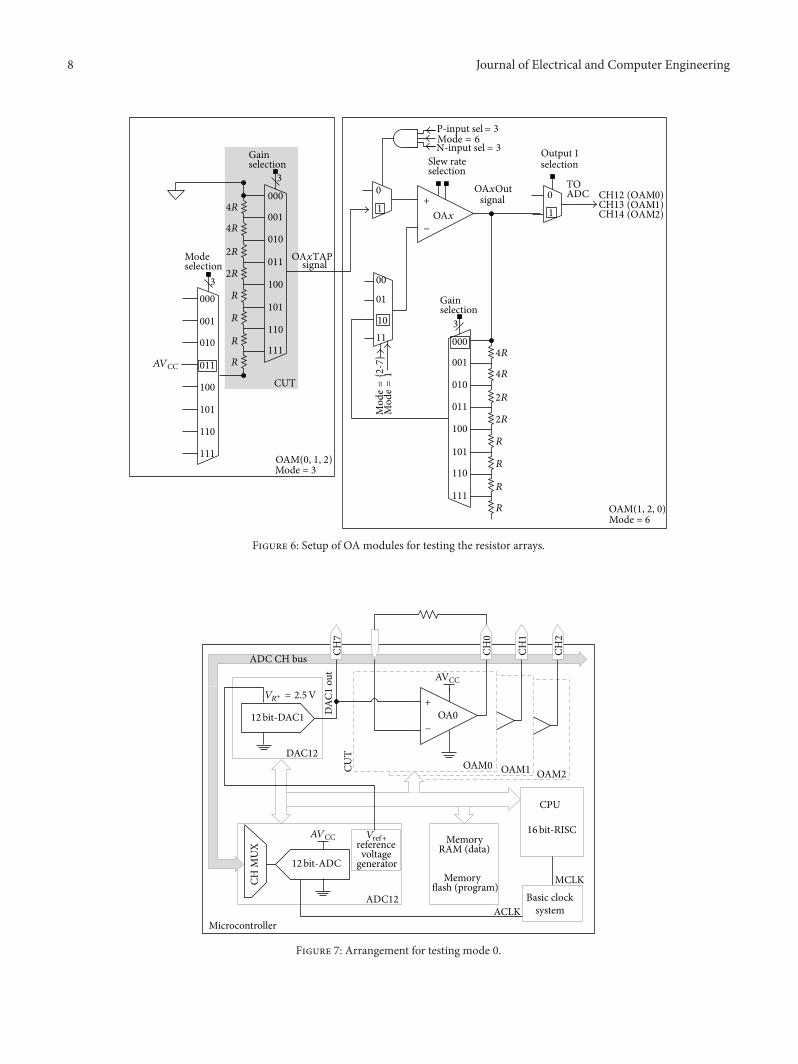
Because it is not possible to measure directly 𝑉OAxTAPthrough an ADC input channel, we propose the schemedepicted in Figure 6. This figure shows the OAMs setup con-figured by the test routine, valid for the three modules. ThesignalOAxTAP is cascaded with the next OAM configured asa unity gain buffer in mode 6. In this way, the ADC acquires(in CH12, CH13, and CH14 for OAM0, OAM1, and OAM2resp.) the programmable𝑉OAxTAP value of the CUT. It shouldbe mentioned that, prior to this test procedure, all OAMs areexercised in mode 6 as unity gain buffer in order to checktheir right operation.
From the measurement of these voltages, the test routinedetermines if all the relations of 𝑅top and 𝑅bottom can beprogrammed and checks if their values are within the limitsspecified by the user. As the resistance ratios establish the gainfor the other module configurations, the routine indirectlytests the correctness of these gain values. Consequently,it would be not necessary to test all the available gainconfigurations in the ACT procedures.
3.2. Mode Configurability Test. To confirm the correct con-figurability of each OAMmode, ACT determines the gain of
the block in different configurations (to be presented in thenext subsection). If this parameter is within the limits allowedby the applications needs, then it is accepted that the testedmode has been properly programmed.
3.2.1. Test of Modes 0 and 1. In both modes, the OAMs areconfigured as unity gain buffers. Mode 0 is designed for usingthe module with external components and all the internalfeedback paths are isolated from the OAs. Consequently, forconfiguring the OA as unity gain buffer, we use the OA pinsto connect the feedback loop. Figure 7 shows the schemeadopted. The feedback path is a wired connection takingadvantage of the existing components on the applicationcircuit board. However, if the configuration of a specificapplication does not include a resistor feedback path, theuse of external analog multiplexers (to switch between testand normal operation mode) is required. Otherwise, thetest procedure for mode 0 (like any other ACT procedure)can be overridden according to the test requirements of theapplication. In mode 1, the OA is configured as unity gainbuffer using a dedicated internal feedback path.
The test procedure is the same for both modes. The OAoutput is connected to the ADC input channel assigned tothe OAxOut pin (OA0, OA1, and OA2 with CH0, CH1, andCH2, resp.). The ADC also acquires the OAM input signal(test stimulus) from the DAC1 output through the CH7.Withthese values, the on-chip processor computes the gain.
3.2.2. Test of Mode 3:Comparator. For testing this mode, weset a fixed voltage level at the noninverter input of the OAs(𝑉+) by using the DAC1 internal connection and program
the inverter input with voltages obtained from the resistorladder. By commuting the ladder between voltages higherand lower than 𝑉
+, it is possible to verify if the comparator
output transitions are between the values reported by thevendor in [18].TheADC acquires the OA output values usingthe internal routing to the ADC CH12, CH13, and CH14 forOAM0, OAM1, and OAM2, respectively.
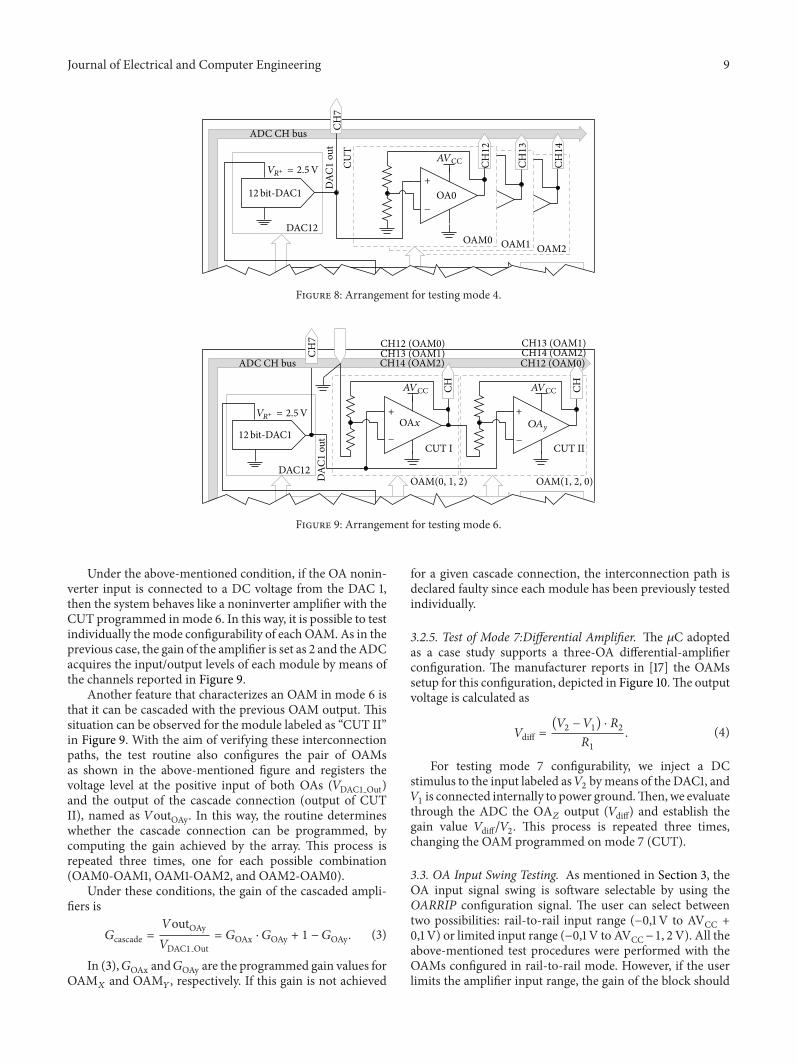
3.2.3. Test of Mode 4:Noninverting PGA. In order to test themode 4 programmability, we set the gain of each OAM as2. As the right operation of the resistor ladder is previouslytested, only one value for the gain is used in the test procedure.As shown in Figure 8, DAC1 is used for exciting the OAMswithDCvoltage levels.TheOAMs input stimulus is registeredthrough the ADC CH7, while the OAs outputs are measuredas in the test of mode 3.
3.2.4. Test of Mode 6:Inverting PGA. When an OAM is con-figured in mode 6 (programmable-gain inverting amplifier),the use of a positive DC voltage level as test stimulus is notuseful because the 𝜇C employs a single supply. Consequently,a negative output swing is not possible. However, for testingmode 6, it is possible to configure the OAM as inverteramplifier but connect internally its input to ground by meansof the proper configuration of the OA input pin. This can beobserved in Figure 9 for the module labeled as “CUT I.”
8 Journal of Electrical and Computer Engineering
000
001
010
011
100
101
110
111
00
01
1011
0
101
CH12 CH13 CH14
Gainselection
3
TOADC000
001
010
011
100
101
110
111
000
001
010
011
100
101
110
111
Gainselection
3
Modeselection
3
CUT
Mode = 3
Mode = 6
signal
= 6
Slew rateselection
+
−
={2
-7}
=1
signal
= 3
= 31
OAx
AVCC
4R
4R
2R
2R
R
R
R
R4R
4R
2R
2R
R
R
R
R
OAx
OAx0)1)2)
OAM(0, 1, 2)
OAM(1, 2, 0)
Figure 6: Setup of OA modules for testing the resistor arrays.
CPU
Microcontroller
referencevoltage
generatorMCLK
MemoryRAM (data)
Memory
ADC12
ADC CH bus
CH M
UX
Basic clock systemACLK
DAC12
+
OAM2
+
OAM1
+
OAM0
CH0
CUT
CH1
CH2
CH7
12bit-DAC1
12bit-ADC
16bit-RISC
OA0+
−
AVCC
Vref+
VR+ = 2.5V
AVCC
DAC
1ou
t
flash (program)
Figure 7: Arrangement for testing mode 0.
Journal of Electrical and Computer Engineering 9
ADC CH bus
DAC12
+
OAM2
+
OAM1
+
OAM0
CH12
CUT
CH13
CH14
CH7
12bit-DAC1 OA0+
−
VR+ = 2.5VAVCC
DAC
1ou
t
Figure 8: Arrangement for testing mode 4.
DAC12
CH
DAC
1 ou
t
CUT I
CH12 (OAM0)CH13 (OAM1)
CH13 (OAM1)CH14 (OAM2)
CUT II
CH7
12bit-DAC1
ADC CH bus
+
−
+
−
CH14 (OAM2)
CHCH
VR+ = 2.5V
CH12 (OAM0)
OAx
AVCC AVCC
OAy
OAM(0, 1, 2) OAM(1, 2, 0)
Figure 9: Arrangement for testing mode 6.
Under the above-mentioned condition, if the OA nonin-verter input is connected to a DC voltage from the DAC 1,then the system behaves like a noninverter amplifier with theCUT programmed inmode 6. In this way, it is possible to testindividually themode configurability of eachOAM. As in theprevious case, the gain of the amplifier is set as 2 and the ADCacquires the input/output levels of each module by means ofthe channels reported in Figure 9.
Another feature that characterizes an OAM in mode 6 isthat it can be cascaded with the previous OAM output. Thissituation can be observed for the module labeled as “CUT II”in Figure 9. With the aim of verifying these interconnectionpaths, the test routine also configures the pair of OAMsas shown in the above-mentioned figure and registers thevoltage level at the positive input of both OAs (𝑉DAC1 Out)and the output of the cascade connection (output of CUTII), named as 𝑉outOAy. In this way, the routine determineswhether the cascade connection can be programmed, bycomputing the gain achieved by the array. This process isrepeated three times, one for each possible combination(OAM0-OAM1, OAM1-OAM2, and OAM2-OAM0).
Under these conditions, the gain of the cascaded ampli-fiers is
𝐺cascade =𝑉outOAy𝑉DAC1 Out
= 𝐺OAx ⋅ 𝐺OAy + 1 − 𝐺OAy. (3)
In (3),𝐺OAx and𝐺OAy are the programmed gain values forOAM
𝑋and OAM
𝑌, respectively. If this gain is not achieved
for a given cascade connection, the interconnection path isdeclared faulty since each module has been previously testedindividually.
3.2.5. Test of Mode 7:Differential Amplifier. The 𝜇C adoptedas a case study supports a three-OA differential-amplifierconfiguration. The manufacturer reports in [17] the OAMssetup for this configuration, depicted in Figure 10.The outputvoltage is calculated as
𝑉diff =(𝑉2− 𝑉1) ⋅ 𝑅2
𝑅1
. (4)
For testing mode 7 configurability, we inject a DCstimulus to the input labeled as𝑉
2bymeans of the DAC1, and
𝑉1is connected internally to power ground.Then,we evaluate
through the ADC the OA𝑍output (𝑉diff) and establish the
gain value 𝑉diff/𝑉2. This process is repeated three times,changing the OAM programmed on mode 7 (CUT).
3.3. OA Input Swing Testing. As mentioned in Section 3, theOA input signal swing is software selectable by using theOARRIP configuration signal. The user can select betweentwo possibilities: rail-to-rail input range (−0,1 V to AVCC +0,1 V) or limited input range (−0,1 V to AVCC−1, 2V). All theabove-mentioned test procedures were performed with theOAMs configured in rail-to-rail mode. However, if the userlimits the amplifier input range, the gain of the block should

10 Journal of Electrical and Computer Engineering
+
+
++
-+
+CUT OAM (1, 2, 0)
Mode = 7
OAM(2, 0, 1)Mode = 6
OAM(0, 1, 2)Mode = 1
OAy
OAZ
−
−
−Vdiff
R1 R2
R1 R2
V1
V2OAx
Figure 10: Three-OA differential amplifier configuration.
be less than the nominal value for input voltage levels nearAVCC.
In order to test the OA input swing programmability,the OAMs configuration depicted in Figure 6 is used. Thetest routine limits the OA
𝑋input range by setting the
OARRIP signal and the resistor ladder is used to set thestimulus levels near AVCC due to the fact that the DACoutput voltage is limited up to 2.5 V. The new OA
𝑋output
measurements are performed as explained in Section 3.1.Theblock gain is computed by means of these measurements andthe registered ones during the resistor ladder test procedures.If the gain of the OA
𝑋module is less than the unit for the
three last test conditions reported in Table 3, then the routinedetermines that the rail-to-rail input mode was successfullydisabled.
3.4. Slew Rate Testing. Each OA has three active modes:slow (0.3 V/𝜇s), medium (0.8V/𝜇s), and fast (1.2 V/𝜇s).Theseslew rate (SR) values are achieved by changing the slew rateselection configuration signals, shown in Figure 4. In order totest the right configuration of this parameter, ACT uses theinternal timer module to measure the time that takes the OAoutput for making a transition from a low voltage level (𝑉OL)to a high one (𝑉OH), for the three active modes.
Figure 11 depicts the scheme adopted for this part ofthe test routine. As observed, the OAM is configured ascomparator. A reference voltage from the resistor ladder andthe DAC1 output are connected to the OAx inputs. Theoutput of each OA under test is connected to a general-purpose digital-input pin with interrupt capability using anexternal wired connection (exclusively for testing purposes).These pins generate an interrupt when there is a low-to-high transition at the OAxOut signal. The routine uses thisinterrupt resource and the Timer-A module, configured atthe lowest available period (125 ns), to accomplish the timemeasurements.
The test procedure is represented in Figure 12(a). Whilethe OA noninverting input voltage 𝑉in+ has a constant levelfrom the DAC1 module, 𝑉in− is switched from a voltage levelhigher than𝑉in+ to a lower one by changing the configuration
of the resistors ladder. This produces a transition at the OAoutput (called 𝑉OAout) from 𝑉OL to 𝑉OH. At the same time,Timer-A is reset and starts a count. When this signal reachesthe threshold voltage of the digital input pin (𝑉IT+), the pingenerates an interruption and the timer is stopped.
According to this figure, the SR can be estimated as
SR =𝑉IT+𝑡sr 𝜇C, (5)
where
𝑡sr 𝜇C = 𝑡TA𝜇C − 𝑡𝑑 − 𝑡int, (6)
𝑡TA𝜇C =1
𝑓clkTA⋅ CountTA. (7)
In (6), 𝑡TA𝜇C is the time measured with Timer-A and 𝑡𝑑
represents the dead time of the OA, defined in this work asthe time required by the OA to reach the 5% of its final valuewhen a step stimulus is applied. On the other hand, 𝑡int is theinterruption processing time and is defined here as follows:the time between the comparator output voltage reaches𝑉IT+and the test routine stops the timer. In (7), CountTA is thecount reached by the Timer-A register and 𝑓clkTA is the workfrequency of the timer.
The parameters 𝑡𝑑, 𝑡int, and𝑉IT+ used by the test routine in
the SR estimation are experimentally determined. For doingthis task, the routine generates an auxiliary signal (𝑉aux𝜇Cin Figure 12) in a digital-output pin that registers the timerevents (when it starts and stops the count). This signal allowsthemeasurements of times and voltage shown in Figure 12(b).The figure presents the results of three measurements ona single OAM, one for each possible SR configuration.However, the measurements have been time-shifted to matchthe low-to-high transition of the signal 𝑉aux𝜇C (stop counttimer event). In this way, the intersection point of the three𝑉OAxOut signals is used as a reference in the measurementof 𝑡int and 𝑉IT+, because these parameters are independentof the SR configuration. Additionally, it is possible to clearlydetermine the different values of 𝑡
𝑑.

Journal of Electrical and Computer Engineering 11
CPU
Microcontroller
MCLK
Basic clock system
DAC12
OAM2
+
OAM1
+
OAM0
CUT
OA2out
DAC1 out
I/O P1
Interrupt capability
MemoryRAM (data)
Memory
Timer A
TA register
referencevoltage
generator
OA1outOA0out
12bit-DAC1
16bit-RISC
OA0+
−
VR+ = 2.5V
Vref+
fTA = 8MHz
AVCC AVCC
port
flash (program)
Figure 11: Arrangement for testing slew rate.
V
Vin−Vin+
VOH
VIT+
tint
VOA outt
ttd
Vaux𝜇C
tsr𝜇CtTA𝜇C
(a)
V
VIT+
tint
t
t
td td td
Vaux𝜇C
slow fastmed
VOA out
(slow) (med)(fast)
(b)
Figure 12: (a) Slewrate test timing diagram. (b) Experimental measurement of 𝑡𝑑, 𝑡int, and 𝑉IT+.
4. Experimental Test Results
The embedded test routine is written in C language as alibrary using IAR Embedded Workbench for TI MSP430C/C++ compiler and amounts to about 3 Kbyte of programmemory in the 𝜇C. For the device used in this application(MSP430FG4619), the total routine execution time is 53.5mswith a CPU clock (main clock, MCLK) of 1MHz. Themeasurement repeatability at free air temperature is evaluatedin order to assess the test precision. For doing this task, thetest procedure is repeated 100 times in each test condition.
Table 4 summarizes the test results for the resistor ladder.It presents the measured values of 𝑉OAxTAP in each testcondition detailed in Table 3, for all the OAMs availablein the device. The mean values shown in the table are ameasure of central tendency, while the maximum (Max) andthe minimum (Min) values are a measure of dispersion. Allthe values depicted in the table are expressed in AVCC units.As can be seen from the data, all measurements present a verylow dispersion around themean value and are very similar forall the OAMs. The maximum deviation is 0.177% (related tothe mean value) for the minimum value of test condition 6

12 Journal of Electrical and Computer Engineering
Table 4: Resistor ladder test experimental results.
Parameter Testcondition Min Mean Max
Voltage level available atthe resistor ladder OA0𝑉OA0TAP (AVCC units)
1 0.2505 0.2506 0.2510
2 0.4999 0.5002 0.5006
3 0.6247 0.6250 0.6256
4 0.7497 0.7500 0.7507
5 0.8122 0.8126 0.8132
6 0.8742 0.8747 0.8750
7 0.9368 0.9371 0.9382
Voltage level available atthe resistor ladder OA1𝑉OA1TAP (AVCC units)
1 0.2505 0.2508 0.2510
2 0.4999 0.5003 0.5006
3 0.6247 0.6249 0.6256
4 0.7492 0.7497 0.7502
5 0.8117 0.8121 0.8122
6 0.8730 0.8746 0.8750
7 0.9355 0.9368 0.9372
Voltage level available atthe resistor ladder OA2𝑉OA2TAP (AVCC units)
1 0.2498 0.2502 0.2505
2 0.4996 0.5000 0.5001
3 0.6247 0.6248 0.6249
4 0.7497 0.7499 0.7507
5 0.8117 0.8122 0.8127
6 0.8730 0.8744 0.8747
7 0.9355 0.9366 0.9372
in OAM1. By another way, the mean values are very close tothe nominal values reported in Table 3.The highest deviationfrom nominal values is 0.323% observed for test condition 1in OAM1. This value can be taken as an indicator of the highaccuracy achieved by ACT.
The experimental results for modes 0, 1, 4, 6, and 7are reported in Table 5. The column labeled as “Parameter”shows the specific gains evaluated by the test routine for eachOAM mode. The column labeled as “Test setup” shows theexpected value for these parameters and gives the value ofthe gain selection signal (see Figure 4). The columns “Min,”“Mean,” and “Max” depict the lowest, mean, and highestvalues of the parameters for the 100 repeated measurements.As in the case of the resistor ladder test, the table showsthat the measurement repeatability is very good for all themodes tested. The highest observed deviation is 1.02% inmode 0. By another way, the mean values are very closeto the expected for each programmed configuration, with amaximum deviation of 0.38% in mode 7.
The test of mode 3 shows that all the OAMs, configuredas comparators, give output excursions between 3.3mV andvalues near AVCC, for the 100 repeated test executions. Thisrange agrees with the data reported by the vendor in thedatasheet [18]. On the other hand, the test results related tothe OA-input swing configurability show that the modulegain (with the range limited) is always less than the unitfor the three last test conditions reported in Table 3. These
values can only be achieved if the rail-to-rail input mode issuccessfully disabled.
Table 6 depicts the experimental results related to theslewrate test procedures, obtained in 100 test executions.The table shows that the slewrate measurements presentvirtually no dispersion, with the exception of the values forthe OA0 and OA2 in “medium” configuration, registering amaximum variation of 9.53% with respect to the main value.As mentioned in Section 3.4, the Timer-A is working at thehighest allowed frequency (8MHz), producing quantizationerrors in the slew rate measurements of 1.532%, 4.226%,and 7.154% for the slow, medium, and fast configurations,respectively.
The quantization error values and the experimental data(reported in Table 6) confirm that ACTdistinguishes changesin the slewrate and consequently is able to test its config-urability because the errors are significantly smaller than thepercentages of variations in the SR produced by a changeof configuration. With the aim of comparison, Table 6 alsoincludes the slewrate typical values reported by the vendor.For all OAs, the mean values are near to the typical ones,suggesting that the measurement is a good estimator of theparameter.
Table 7 shows the auxiliary measurements of times usedin the slewrate estimation: interrupt processing time (𝑡int) anddead time (𝑡
𝑑). The values in the table are the result of the
measurements performed experimentally in laboratory. As

Journal of Electrical and Computer Engineering 13
Table 5: Modes test experimental results.
Test mode Parameter Test setup Min Mean Max
Mode 0Unity gain OAM0 0.9939 1.0013 1.0075Unity gain OAM1 0.9917 1.0010 1.0083Unity gain OAM2 0.9947 1.0011 1.0114
Mode 1Unity gain OAM0 0.9969 1.0026 1.0091Unity gain OAM1 0.9954 1.0025 1.0098Unity gain OAM2 0.9916 0.9979 1.0045
Mode 4Gain OAM0
Programmed gain = +2Gain selection = 2
1.9879 2.0036 2.0167Gain OAM1 1.9924 2.0041 2.0182Gain OAM2 1.9894 2.0025 2.0152
Mode 6
Gain OAM0Programmed gain = +2Gain selection = 2
1.9894 2.0020 2.0198Gain OAM1 1.9894 2.0029 2.0167Gain OAM2 1.9939 2.0035 2.0167
Gain OAM2-OAM0in cascade
Programmed gain = 0.665Gain selection OAM2 = 1Gain selection OAM0 = 2
0.6626 0.6672 0.6727
Gain OAM0-OAM1in cascade
Programmed gain = 0.665Gain selection OAM0 = 1Gain selection OAM1 = 2
0.6619 0.6668 0.6717
Gain OAM1-OAM2in cascade
Programmed gain = 0.665Gain selection OAM1 = 1Gain selection OAM2 = 2
0.6611 0.6671 0.6709
Mode 7
Gain of arrangementOAM0-OAM1-OAM2
Programmed gain = 1.666CUT = OAM1 1.6591 1.6724 1.6823
Gain of arrangementOAM1-OAM2-OAM0
Programmed gain = 1.666CUT = OAM2 1.6591 1.6721 1.6818
Gain of arrangementOAM2-OAM0-OAM1
Programmed gain = 1.666CUT = OAM0 1.6601 1.6730 1.6859
Table 6: Slew-rate test experimental results.
Parameter Programmed slew rate Typical Min Mean Max
Slew rate OA0 (V/𝜇s)Slow 0.300 0.255 0.255 0.255
Medium 0.800 0.702 0.743 0.770Fast 1.200 1.226 1.226 1.226
Slew rate OA1 (V/𝜇s)Slow 0.300 0.264 0.264 0.264
Medium 0.800 0.770 0.770 0.770Fast 1.200 1.226 1.226 1.226
Slew rate OA2 (V/𝜇s)Slow 0.300 0.240 0.240 0.240
Medium 0.800 0.702 0.703 0.770Fast 1.200 1.226 1.226 1.226
Table 7: Slew rate test auxiliary measurements.
Programmedslew rate
Interrupt processingtime 𝑡int (𝜇s)
Dead time𝑡𝑑(𝜇s)
Slow 2.3 7.92Medium 2.3 2.62Fast 2.3 1.58
14 Journal of Electrical and Computer Engineering
can be seen from the table, 𝑡int value is independent of theOAMconfiguration because it only depends on the frequencyof the CPU clock (MCLK).
5. Conclusions
In this paper, we address the application of the ACT approachto an EACC composed of operational amplifiers and inter-connection resources of a modern 𝜇C.The proposed schemeallows establishing the correct configurability of the CUT andchecks the proper behavior of the resistor arrays. The testprocedures were successfully adapted to the requirements ofthe addressedEACC.Thenegligible hardware overhead of theapproach allows using it as a low-cost self-test procedure formaintenance purposes in applications that require minimiz-ing power and cost. The test strategy is experimentally evalu-ated in a WSN node with multisensor interface capability inorder to demonstrate the ACT approach applicability in thecontext of a real application. The experimental results showvery good repeatability, with very low errors. These resultsallow concluding that the approach proposed here is usefulfor testing the functionality of the CUT using a simple andvery low-cost strategy.
Conflict of Interests
The authors declare that there is no conflict of interests regar-ding the publication of this paper.
References
[1] R. Rajsuman, “Testing of analog and mixed-signal cores,” inSystem-on-Chip: Design and Test, pp. 181–205, Advantest Amer-ica R&D Center, Santa Clara, Calif, USA, 2000.
[2] B. Vinnakota and R. Harjani, “Introduction,” inAnalog andMi-xed-Signal Test, B. Vinnakota, Ed., pp. 1–14, PrenticeHall, UpperSaddle River, NJ, USA, 1998.
[3] I. Grout, Integrated Circuit Test Engineering:Modern Techniques,Springer, London, UK, 2006.
[4] F. F. Dai and C. E. Stroud, “Analog and mixed-signal test arch-itectures,” in System-on-Chip Test Architectures: Nanometer De-sign for Testability, L. T. Wang, C. E. Stroud, and N. A. Touba,Eds., pp. 703–741, Morgan Kaufmann, Burlington, Mass, USA,2008.
[5] D. Gizopoulus, Advances in Electronic Testing: Challenges andMethodologies, Springer, Amsterdam, The Netherlands, 2006.
[6] T. R. Balen, A. Andrade Jr., F. Azaıs, M. Lubaszewski, and M.Renovell, “Applying the oscillation test strategy to FPAA’s con-figurable analog blocks,” Journal of Electronic Testing, vol. 21, no.2, pp. 135–146, 2005.
[7] T. Balen, A. Andrade Jr., F. Azaıs, M. Lubaszewski, andM. Ren-ovell, “An approach to the built-in self-test of field program-mable analog arrays,” in Proceedings of the 22nd IEEE VLSI TestSymposium, pp. 383–388, April 2004.
[8] T. Balen, A.Andrade Jr., F. Azaıs,M. Lubaszewski, andM.Reno-vell, “Testing the configurable analog blocks of field programm-able analog arrays,” in Proceedings of the International Test Con-ference, pp. 893–902, October 2004.
[9] T. Balen, J. V. Calvano, M. S. Lubaszewski, and M. Renovell,“Built-in self-test of field programmable analog arrays based on
transient response analysis,” Journal of Electronic Testing, vol. 23,no. 6, pp. 497–512, 2007.
[10] T. Balen, J. V. Calvano, M. S. Lubaszewski, and M. Renovell,“Functional test of field programmable analog arrays,” in Pro-ceedings of the 24th IEEE VLSI Test Symposium, pp. 333–339,Berkeley,California, USA, May 2006.
[11] A. Andrade Jr., G. Vieira, T. R. Balen, M. Lubaszewski, F. Azaıs,and M. Renovell, “Built-in self-test of global interconnects offield programmable analog arrays,” Microelectronics Journal,vol. 36, no. 12, pp. 1112–1123, 2005.
[12] G. Pereira, A. Andrade Jr., T. Balen, M. Lubaszewski, F. Azais,and M. Renovell, “Testing the interconnect networks and I/Oresources of field programmable analog arrays,” in Proceedingsof the 23rd IEEE VLSI Test Symposium, pp. 389–394, 2005.
[13] D. Grzechca, T. Golonek, and J. Rutkowski, “Diagnosis of spe-cification parametric faults in the FPAA—the RBF neural net-work approach,” in Proceedings of the 2nd European ComputingConference (ECC ’08), pp. 275–280, 2008.
[14] A. Laprovitta, G. Peretti, E. Romero, and S.Mourad, “A low-costconfigurability test strategy for an embedded analog circuit,”Microelectronic Journal, vol. 43, no. 11, pp. 745–755, 2012.
[15] A. Krstic, L. Chen, W. C. Lai, K. T. Cheng, and S. Dey, “Em-bedded software-based self-test for programmable core-baseddesigns,” IEEE Design and Test of Computers, vol. 19, no. 4, pp.18–27, 2002.
[16] R. Rajsuman, “Testing a system-on-a-chip with embeddedmic-roprocessor,” in Proceedings of the International Test Conference(ITC ’99), pp. 499–508, September 1999.
[17] Texas Instruments, Chapter 22-OA, in: MSP430x4xx FamilyUser’s Guide-SLAU056J, 2010.
[18] Texas Instruments,MSP430xG461xMixed SignalMicrocontro-ller Datasheet-SLAS508I, 2011.
[19] Texas Instruments, Chapter 18-OA, in: MSP430x2xx FamilyUser’s Guide-SLAU144E, 2008.

International Journal of
AerospaceEngineeringHindawi Publishing Corporationhttp://www.hindawi.com Volume 2014
RoboticsJournal of
Hindawi Publishing Corporationhttp://www.hindawi.com Volume 2014
Hindawi Publishing Corporationhttp://www.hindawi.com Volume 2014
Active and Passive Electronic Components
Control Scienceand Engineering
Journal of
Hindawi Publishing Corporationhttp://www.hindawi.com Volume 2014
International Journal of
RotatingMachinery
Hindawi Publishing Corporationhttp://www.hindawi.com Volume 2014
Hindawi Publishing Corporation http://www.hindawi.com
Journal ofEngineeringVolume 2014
Submit your manuscripts athttp://www.hindawi.com
VLSI Design
Hindawi Publishing Corporationhttp://www.hindawi.com Volume 2014
Hindawi Publishing Corporationhttp://www.hindawi.com Volume 2014
Shock and Vibration
Hindawi Publishing Corporationhttp://www.hindawi.com Volume 2014
Civil EngineeringAdvances in
Acoustics and VibrationAdvances in
Hindawi Publishing Corporationhttp://www.hindawi.com Volume 2014
Hindawi Publishing Corporationhttp://www.hindawi.com Volume 2014
Electrical and Computer Engineering
Journal of
Advances inOptoElectronics
Hindawi Publishing Corporation http://www.hindawi.com
Volume 2014
The Scientific World JournalHindawi Publishing Corporation http://www.hindawi.com Volume 2014
SensorsJournal of
Hindawi Publishing Corporationhttp://www.hindawi.com Volume 2014
Modelling & Simulation in EngineeringHindawi Publishing Corporation http://www.hindawi.com Volume 2014
Hindawi Publishing Corporationhttp://www.hindawi.com Volume 2014
Chemical EngineeringInternational Journal of Antennas and
Propagation
International Journal of
Hindawi Publishing Corporationhttp://www.hindawi.com Volume 2014
Hindawi Publishing Corporationhttp://www.hindawi.com Volume 2014
Navigation and Observation
International Journal of
Hindawi Publishing Corporationhttp://www.hindawi.com Volume 2014
DistributedSensor Networks
International Journal of