research on extending and surpassing the limits of...
TRANSCRIPT
RRD 3/21/07
Research on Extending and
Surpassing the Limits of CMOS
Research on Extending and
Surpassing the Limits of CMOS
IEEE Circuits and Systems Society
DFW Chapter 3/07 Seminar
Dallas, Texas
March 21, 2007
Dr. Robert Doering
Texas Instruments
RRD 3/21/07
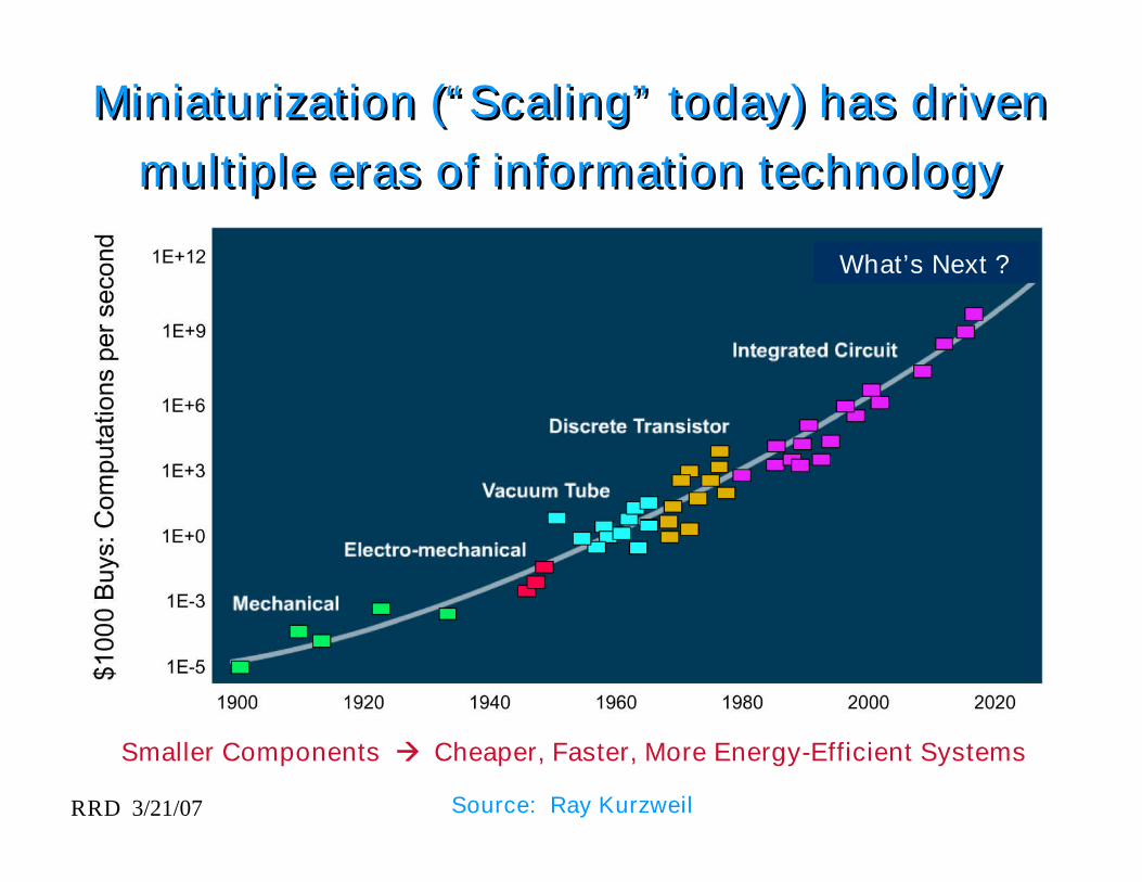
Miniaturization (“Scaling” today) has drivenmultiple eras of information technology
Miniaturization (“Scaling” today) has drivenmultiple eras of information technology
What’s Next ?
Source: Ray Kurzweil
Smaller Components Cheaper, Faster, More Energy-Efficient Systems
RRD 3/21/07
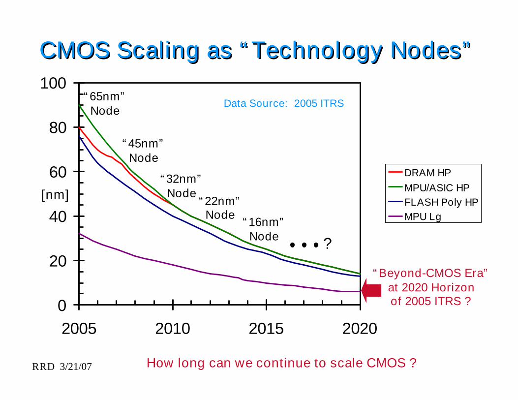
CMOS Scaling as “Technology Nodes”CMOS Scaling as “Technology Nodes”
0
20
40
60
80
100
2005 2010 2015 2020
DRAM HPMPU/ASIC HPFLASH Poly HPMPU Lg
[nm]
“Beyond-CMOS Era”at 2020 Horizonof 2005 ITRS ?
“65nm”Node
“45nm”Node
“32nm”Node
“22nm”Node
“16nm”Node
Data Source: 2005 ITRS
?
How long can we continue to scale CMOS ?
RRD 3/21/07
U.S.A.SIA Korea
KSIAJapan
JEITA
TaiwanTSIA
EuropeESIA
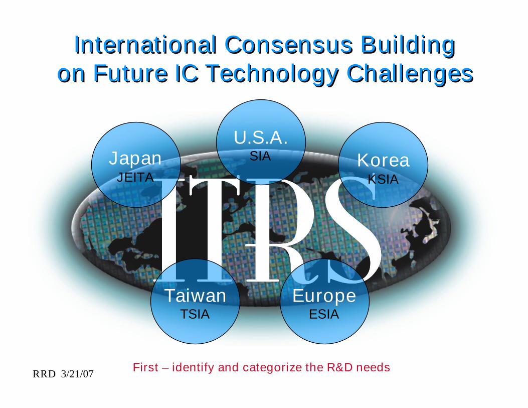
International Consensus Buildingon Future IC Technology Challenges
International Consensus Buildingon Future IC Technology Challenges
First – identify and categorize the R&D needs
RRD 3/21/07
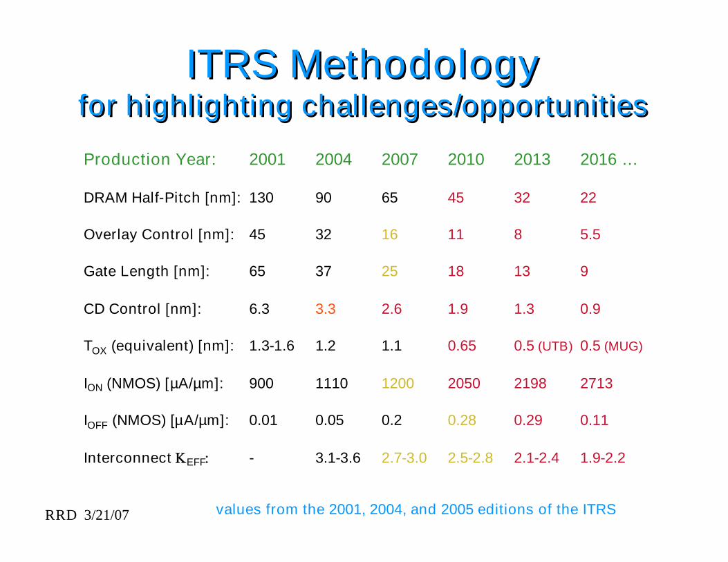
Production Year: 2001 2004 2007 2010 2013 2016 …
DRAM Half-Pitch [nm]: 130 90 65 45 32 22
Overlay Control [nm]: 45 32 16 11 8 5.5
Gate Length [nm]: 65 37 25 18 13 9
CD Control [nm]: 6.3 3.3 2.6 1.9 1.3 0.9
TOX (equivalent) [nm]: 1.3-1.6 1.2 1.1 0.65 0.5 (UTB) 0.5 (MUG)
ION (NMOS) [µA/µm]: 900 1110 1200 2050 2198 2713
IOFF (NMOS) [µA/µm]: 0.01 0.05 0.2 0.28 0.29 0.11
Interconnect EFF - 3.1-3.6 2.7-3.0 2.5-2.8 2.1-2.4 1.9-2.2
ITRS Methodologyfor highlighting challenges/opportunities
ITRS Methodologyfor highlighting challenges/opportunities
values from the 2001, 2004, and 2005 editions of the ITRS
RRD 3/21/07
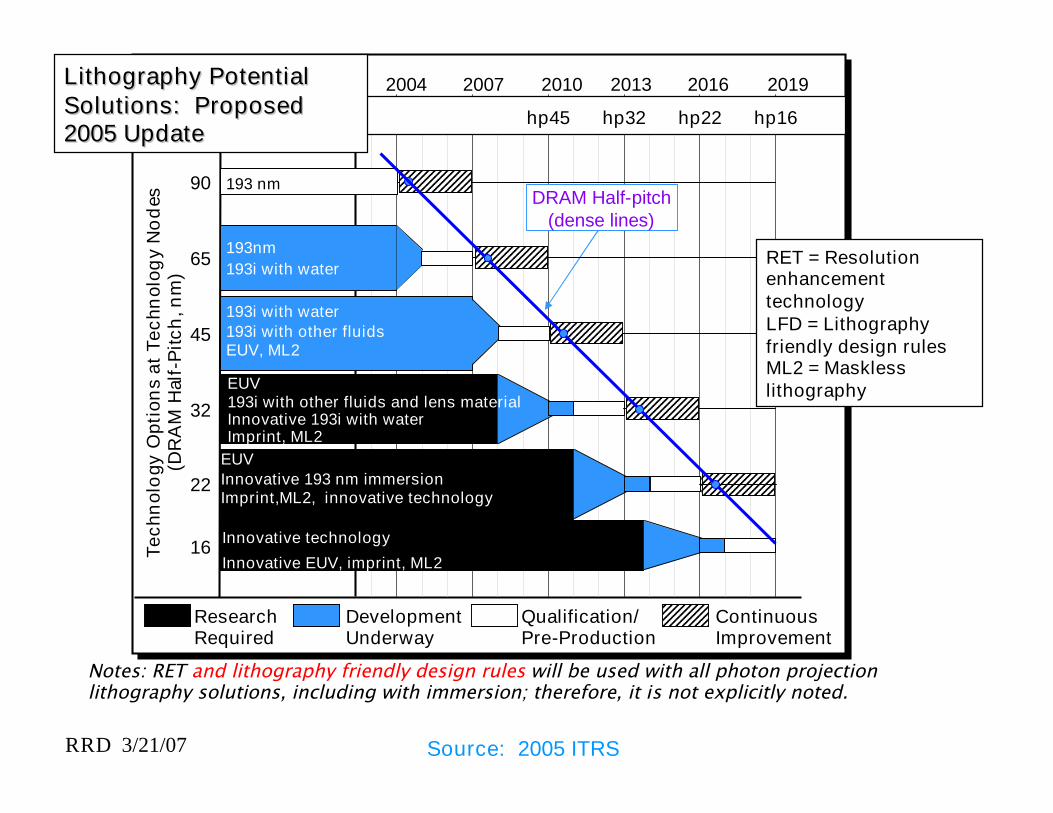
Notes: RET and lithography friendly design rules will be used with all photon projectionlithography solutions, including with immersion; therefore, it is not explicitly noted.
Technology Node
2007 2013 20192004 20162010
hp32 hp16hp22hp45
ResearchRequired
DevelopmentUnderway
Qualification/Pre-Production
ContinuousImprovement
DRAM Half-pitch(dense lines)
Tech
nol
ogy
Opt
ion
sat
Tech
nol
ogy
No
des
(DR
AM
Hal
f-P
itch
,nm
)90 193 nm
65193nm193i with water
32EUV193i with other fluids and lens materialInnovative 193i with waterImprint, ML2
22
16 Innovative technology
Innovative EUV, imprint, ML2
45193i with water193i with other fluidsEUV, ML2
RET = ResolutionenhancementtechnologyLFD = Lithographyfriendly design rulesML2 = Masklesslithography
Lithography PotentialLithography PotentialSolutions: ProposedSolutions: Proposed2005 Update2005 Update
EUVInnovative 193 nm immersionImprint,ML2, innovative technology
Source: 2005 ITRS
RRD 3/21/07
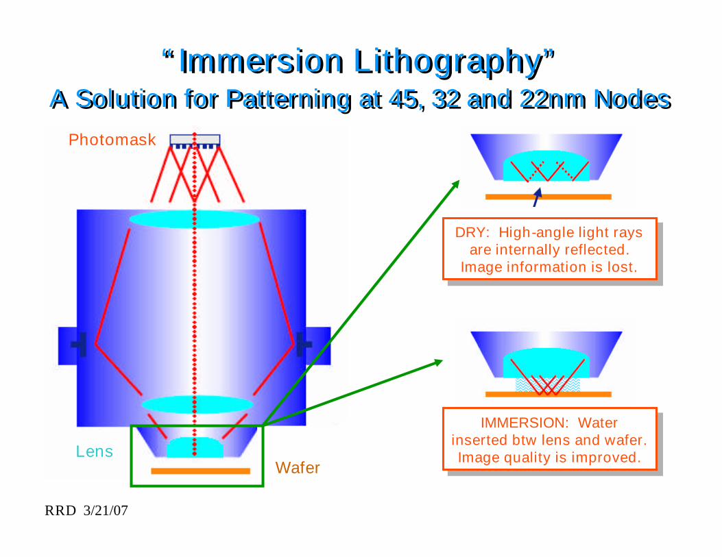
DRY: High-angle light raysare internally reflected.
Image information is lost.
DRY: High-angle light raysare internally reflected.
Image information is lost.
IMMERSION: Waterinserted btw lens and wafer.Image quality is improved.
IMMERSION: Waterinserted btw lens and wafer.Image quality is improved.
“Immersion Lithography”A Solution for Patterning at 45, 32 and 22nm Nodes
“Immersion Lithography”A Solution for Patterning at 45, 32 and 22nm Nodes
Photomask
WaferLens
RRD 3/21/07
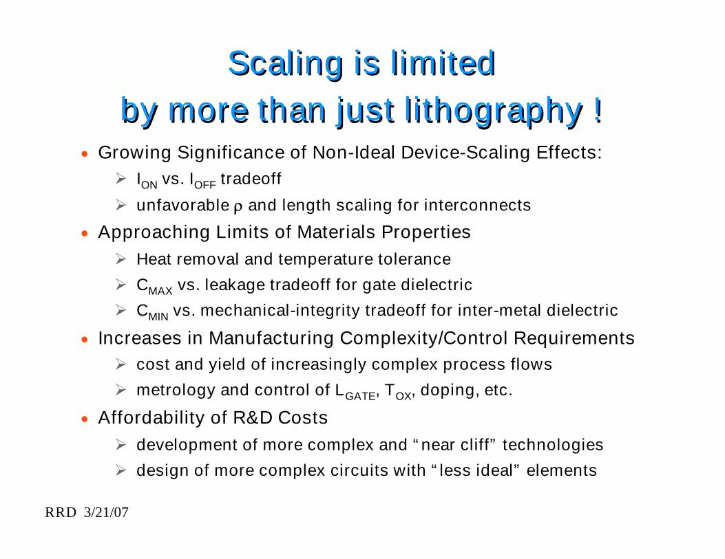
Scaling is limitedby more than just lithography !
Scaling is limitedby more than just lithography !
Growing Significance of Non-Ideal Device-Scaling Effects: ION vs. IOFF tradeoff
unfavorable and length scaling for interconnects
Approaching Limits of Materials Properties Heat removal and temperature tolerance
CMAX vs. leakage tradeoff for gate dielectric
CMIN vs. mechanical-integrity tradeoff for inter-metal dielectric
Increases in Manufacturing Complexity/Control Requirements cost and yield of increasingly complex process flows
metrology and control of LGATE, TOX, doping, etc.
Affordability of R&D Costs development of more complex and “near cliff” technologies
design of more complex circuits with “less ideal” elements
RRD 3/21/07
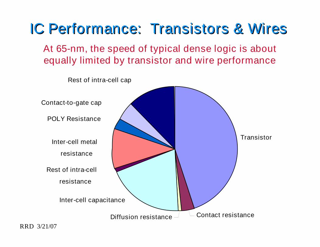
At 65-nm, the speed of typical dense logic is aboutequally limited by transistor and wire performance
Transistor
Contact resistanceDiffusion resistance
Inter-cell capacitance
Rest of intra-cell
resistance
Inter-cell metal
resistance
POLY Resistance
Contact-to-gate cap
Rest of intra-cell cap
IC Performance: Transistors & WiresIC Performance: Transistors & Wires
RRD 3/21/07
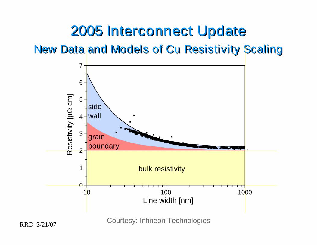
2005 Interconnect UpdateNew Data and Models of Cu Resistivity Scaling
2005 Interconnect UpdateNew Data and Models of Cu Resistivity Scaling
10 100 10000
1
2
3
4
5
6
7
sidewall
grainboundary
bulk resistivity
Res
istiv
ity[µ
cm]
Line width [nm]
Courtesy: Infineon Technologies
RRD 3/21/07
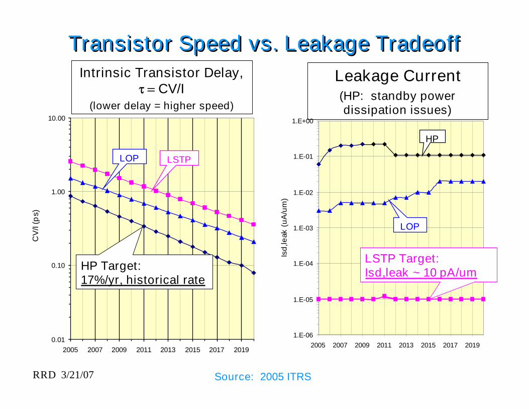
Intrinsic Transistor Delay,CV/I
(lower delay = higher speed)
Leakage Current(HP: standby powerdissipation issues)
Preliminary Results
0.01
0.10
1.00
10.00
2005 2007 2009 2011 2013 2015 2017 2019
Calendar Year
CV
/I(p
s)(p
s)
1.E-06
1.E-05
1.E-04
1.E-03
1.E-02
1.E-01
1.E+00
2005 2007 2009 2011 2013 2015 2017 2019
Calendar year
Isd
,leak
(uA
/um
)
HP Target:17%/yr, historical rate
LOP LSTP
LSTP Target:Isd,leak ~ 10 pA/um
LOP
HP
Transistor Speed vs. Leakage TradeoffTransistor Speed vs. Leakage Tradeoff
Source: 2005 ITRS
RRD 3/21/07
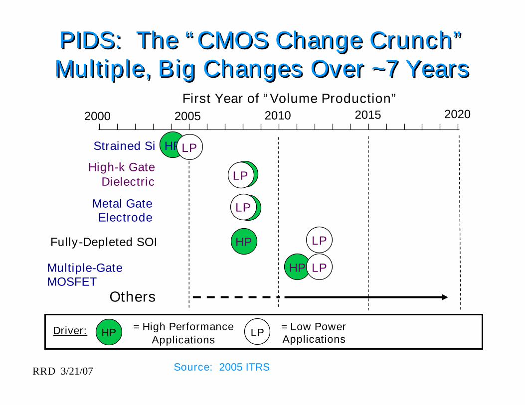
2000 2005 2010 2015 2020First Year of “Volume Production”
High-k GateDielectric HPLP
LPHP = High PerformanceApplications
= Low PowerApplications
Driver:
Others
Fully-Depleted SOI HP LP
Multiple-GateMOSFET
HP LP
HPStrained Si LP
HPMetal GateElectrode
LP
PIDS: The “CMOS Change Crunch”Multiple, Big Changes Over ~7 YearsPIDS: The “CMOS Change Crunch”Multiple, Big Changes Over ~7 Years
Source: 2005 ITRS
RRD 3/21/07
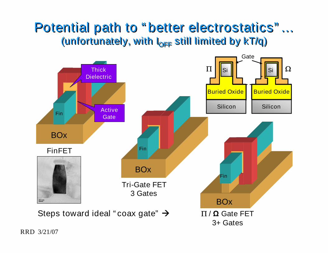
Fin
BOx
Tri-Gate FET3 Gates
Fin
BOx/ ΩGate FET
3+ Gates
Fin
BOx
FinFET2 Gates
ThickDielectric
ActiveGate
Potential path to “better electrostatics”…(unfortunately, with IOFF still limited by kT/q)
Potential path to “better electrostatics”…(unfortunately, with IOFF still limited by kT/q)
Buried Oxide
Silicon
Si Si
Gate
Buried Oxide
Silicon
Steps toward ideal “coax gate”
20 nm
RRD 3/21/07
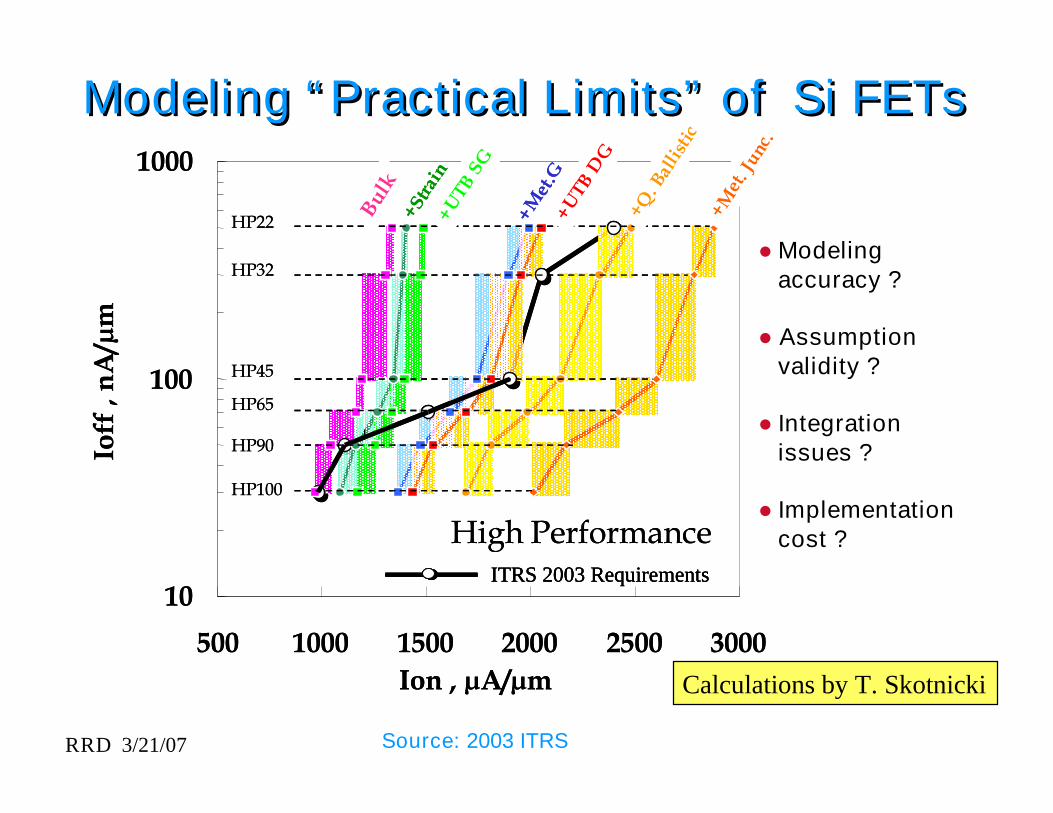
10
100
1000
500 1000 1500 2000 2500 3000Ion , µA/µm
Ioff
,nA
/µm
HP100
HP90
HP65
HP45
HP32
HP22 Bulk
+Stra
in+U
TBSG
+Met
.G+U
TBD
G
+Q. B
allis
tic+M
et. J
unc.
High PerformanceITRS 2003 Requirements
10
100
1000
500 1000 1500 2000 2500 3000Ion , µA/µm
Ioff
,nA
/µm
HP100
HP90
HP65
HP45
HP32
HP22 Bulk
+Stra
in+U
TBSG
+Met
.G+U
TBD
G
+Q. B
allis
tic+M
et. J
unc.
High PerformanceITRS 2003 RequirementsITRS 2003 Requirements
Calculations by T. Skotnicki
●Modelingaccuracy ?
●Assumptionvalidity ?
●Integrationissues ?
●Implementationcost ?
Source: 2003 ITRS
Modeling “Practical Limits” of Si FETsModeling “Practical Limits” of Si FETs
RRD 3/21/07
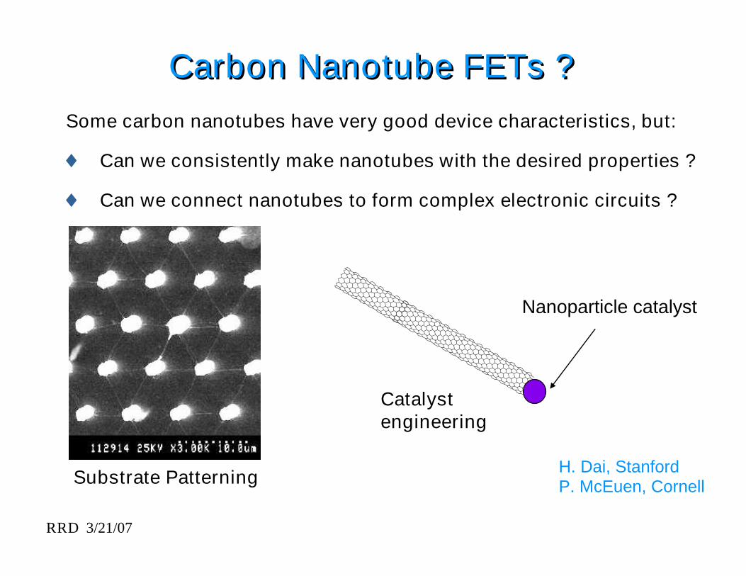
Substrate Patterning H. Dai, StanfordP. McEuen, Cornell
Catalystengineering
Nanoparticle catalyst
Carbon Nanotube FETs ?Carbon Nanotube FETs ?Some carbon nanotubes have very good device characteristics, but:
Can we consistently make nanotubes with the desired properties ?
Can we connect nanotubes to form complex electronic circuits ?
RRD 3/21/07
RRD 3/21/07
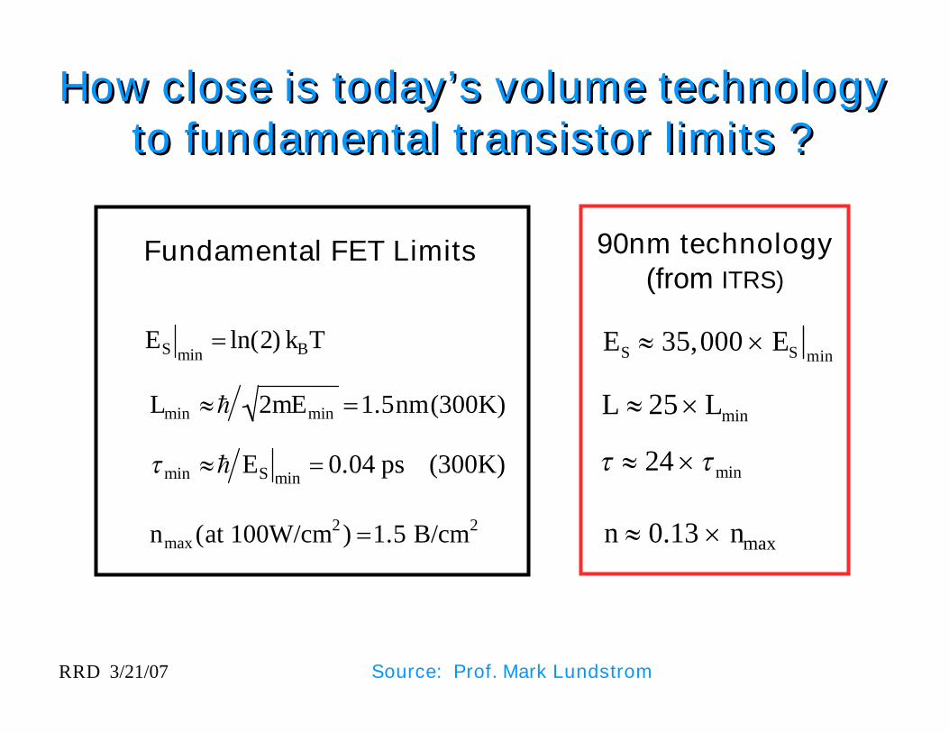
How close is today’s volume technologyto fundamental transistor limits ?
How close is today’s volume technologyto fundamental transistor limits ?
ES minln(2) kBT
Lmin 2mEmin 1.5nm(300K)
min ES min0.04 ps (300K)
Fundamental FET Limits
nmax (at 100W/cm2) 1.5 B/cm2
90nm technology(from ITRS)
ES 35,000 ES min
L 25Lmin
24 min
Source: Prof. Mark Lundstrom
n 0.13 nmax
RRD 3/21/07
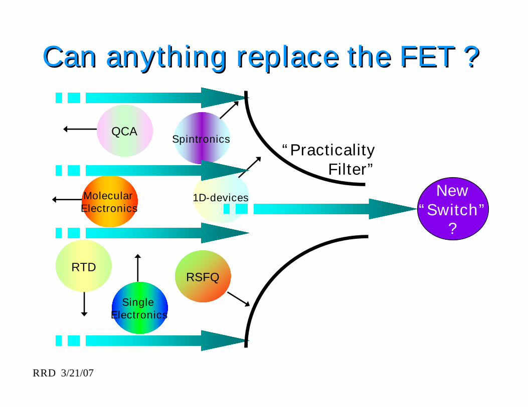
Can anything replace the FET ?Can anything replace the FET ?
QCA
RTD
SingleElectronics
MolecularElectronics
RSFQ
Spintronics
1D-devices New“Switch”
?
“PracticalityFilter”
RRD 3/21/07
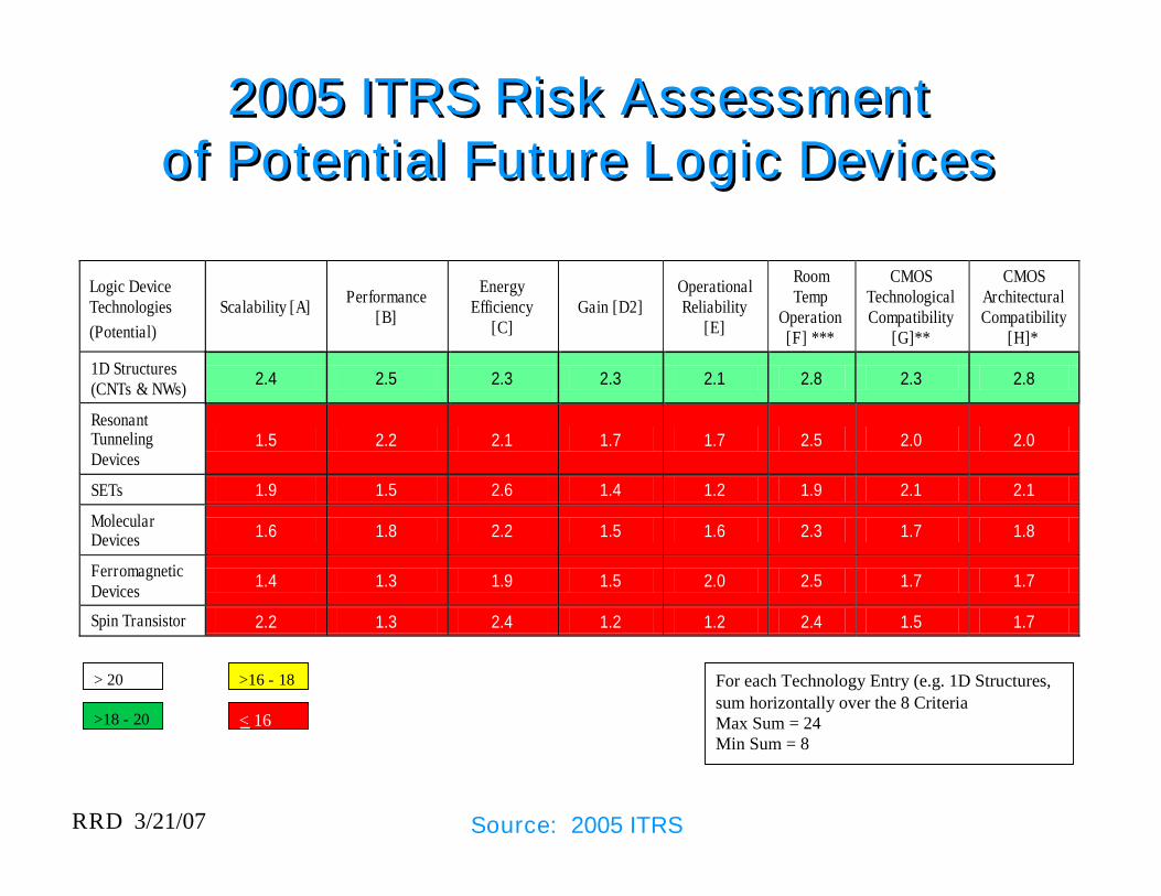
Logic DeviceTechnologies(Potential)
Scalability [A] Performance[B]
EnergyEfficiency
[C]Gain [D2]
OperationalReliability
[E]
RoomTemp
Operation[F] ***
CMOSTechnologicalCompatibility
[G]**
CMOSArchitecturalCompatibility
[H]*
1D Structures(CNTs & NWs) 2.4 2.5 2.3 2.3 2.1 2.8 2.3 2.8
ResonantTunnelingDevices
1.5 2.2 2.1 1.7 1.7 2.5 2.0 2.0
SETs 1.9 1.5 2.6 1.4 1.2 1.9 2.1 2.1
MolecularDevices 1.6 1.8 2.2 1.5 1.6 2.3 1.7 1.8
FerromagneticDevices 1.4 1.3 1.9 1.5 2.0 2.5 1.7 1.7
Spin Transistor 2.2 1.3 2.4 1.2 1.2 2.4 1.5 1.7
For each Technology Entry (e.g. 1D Structures,sum horizontally over the 8 CriteriaMax Sum = 24Min Sum = 8
> 20
>18 - 20 < 16
>16 - 18
2005 ITRS Risk Assessmentof Potential Future Logic Devices
2005 ITRS Risk Assessmentof Potential Future Logic Devices
Source: 2005 ITRS
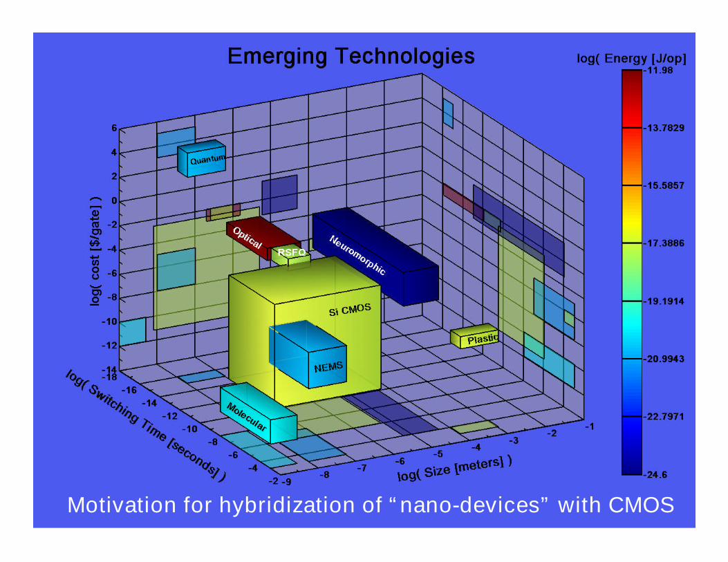
RRD 3/21/07Motivation for hybridization of “nano-devices” with CMOS
SRC/File name/ 21S.T.08.05.05
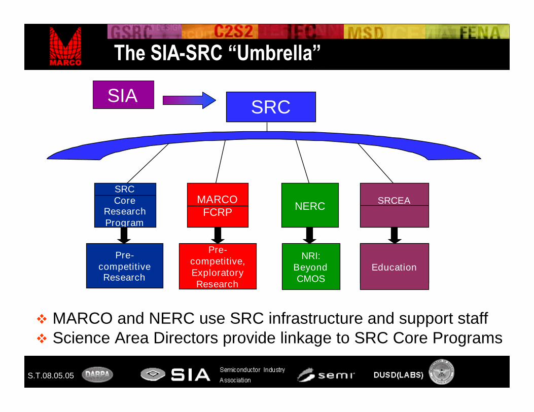
The SIA-SRC “Umbrella”
MARCOFCRP
SRCCore
ResearchProgram
SRC
NERC SRCEA
Pre-competitiveResearch
Pre-competitive,ExploratoryResearch
SIAParticipants &
others
NRI:BeyondCMOS
Education
MARCO and NERC use SRC infrastructure and support staff Science Area Directors provide linkage to SRC Core Programs
SIA
RRD 3/21/07 Source: MARCO, 2004
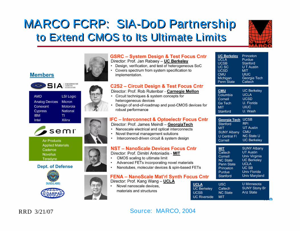
MARCO FCRP: SIA-DoD Partnershipto Extend CMOS to Its Ultimate Limits
MARCO FCRP: SIA-DoD Partnershipto Extend CMOS to Its Ultimate Limits
RRD 3/21/07
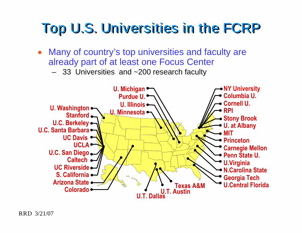
Many of country’s top universities and faculty arealready part of at least one Focus Center– 33 Universities and ~200 research faculty
Top U.S. Universities in the FCRPTop U.S. Universities in the FCRP
U.T. Dallas
U. MichiganPurdue U.U. Illinois
U. Minnesota
Columbia U.Cornell U.RPIStony BrookU. at AlbanyMITPrincetonCarnegie MellonPenn State U.U.VirginiaN.Carolina StateGeorgia TechU.Central Florida
U.T. Austin
U. WashingtonStanford
U.C. BerkeleyU.C. Santa Barbara
UC DavisUCLA
U.C. San DiegoCaltech
UC RiversideS. California
Arizona StateColorado
NY University
Texas A&M
RRD 3/21/07
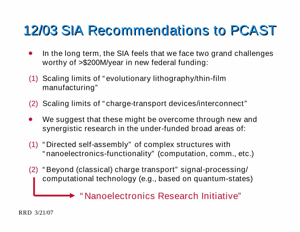
12/03 SIA Recommendations to PCAST12/03 SIA Recommendations to PCAST
In the long term, the SIA feels that we face two grand challengesworthy of >$200M/year in new federal funding:
(1) Scaling limits of “evolutionary lithography/thin-filmmanufacturing”
(2) Scaling limits of “charge-transport devices/interconnect”
We suggest that these might be overcome through new andsynergistic research in the under-funded broad areas of:
(1) “Directed self-assembly” of complex structures with“nanoelectronics-functionality” (computation, comm., etc.)
(2) “Beyond (classical) charge transport” signal-processing/computational technology (e.g., based on quantum-states)
“Nanoelectronics Research Initiative”

RRD 3/21/07
The Search for a “New Switch”:
The NERC Consortium NRI ProgramThe Search for a “New Switch”:
The NERC Consortium NRI Program
NERC members: AMD, Intel, IBM , Freescale, Micron, TI
Started in March, 2005
First project: partnership with NSF on supplementalfunding for selected N/MR-SECs on nanoelectronics
NERC-NSF award announcements at SNB-III, 12/05
Latest program: formation of three regional NRICenters in partnership with state governments, et al.
RRD 3/21/07
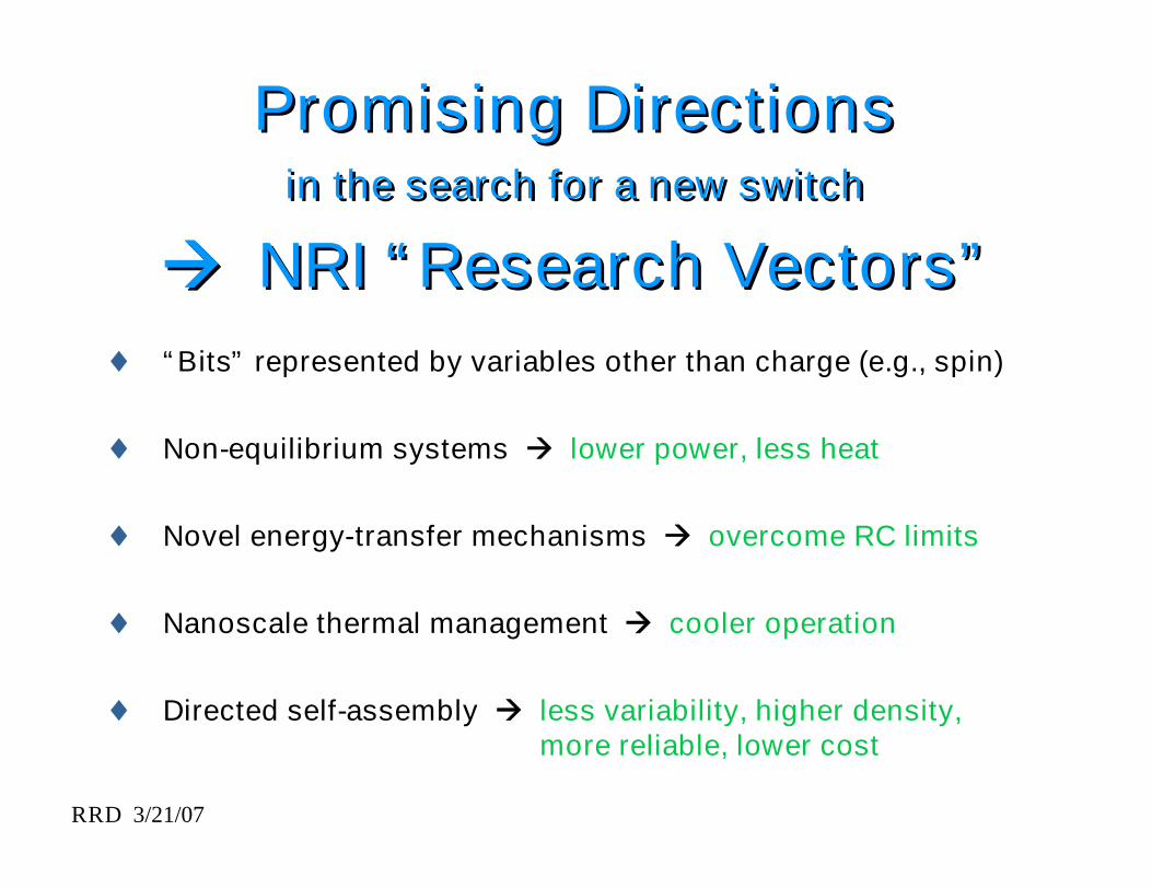
Promising Directionsin the search for a new switch
NRI “Research Vectors”
Promising Directionsin the search for a new switch
NRI “Research Vectors” “Bits” represented by variables other than charge (e.g., spin)
Non-equilibrium systems lower power, less heat
Novel energy-transfer mechanisms overcome RC limits
Nanoscale thermal management cooler operation
Directed self-assembly less variability, higher density,more reliable, lower cost
RRD 3/21/07
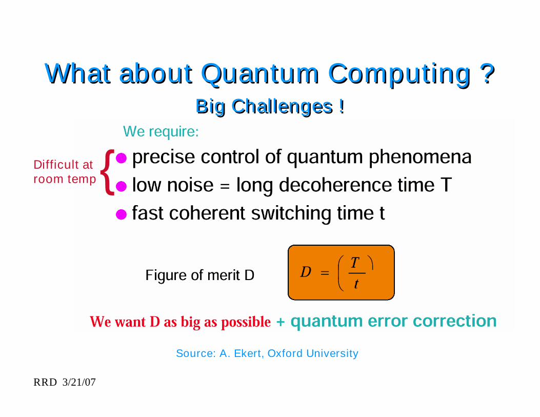
What about Quantum Computing ?Big Challenges !
What about Quantum Computing ?Big Challenges !
Source: A. Ekert, Oxford University
Difficult atroom temp
RRD 3/21/07
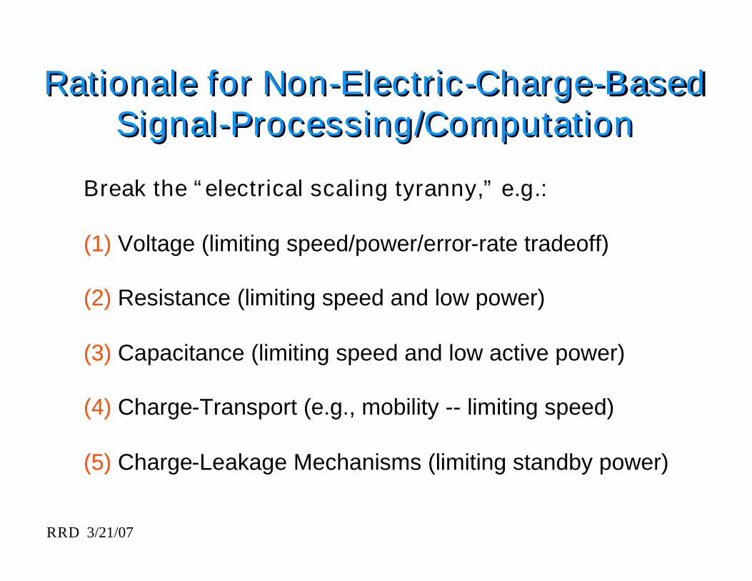
Rationale for Non-Electric-Charge-BasedSignal-Processing/Computation
Rationale for Non-Electric-Charge-BasedSignal-Processing/Computation
Break the “electrical scaling tyranny,” e.g.:
(1) Voltage (limiting speed/power/error-rate tradeoff)
(2) Resistance (limiting speed and low power)
(3) Capacitance (limiting speed and low active power)
(4) Charge-Transport (e.g., mobility -- limiting speed)
(5) Charge-Leakage Mechanisms (limiting standby power)
RRD 3/21/07
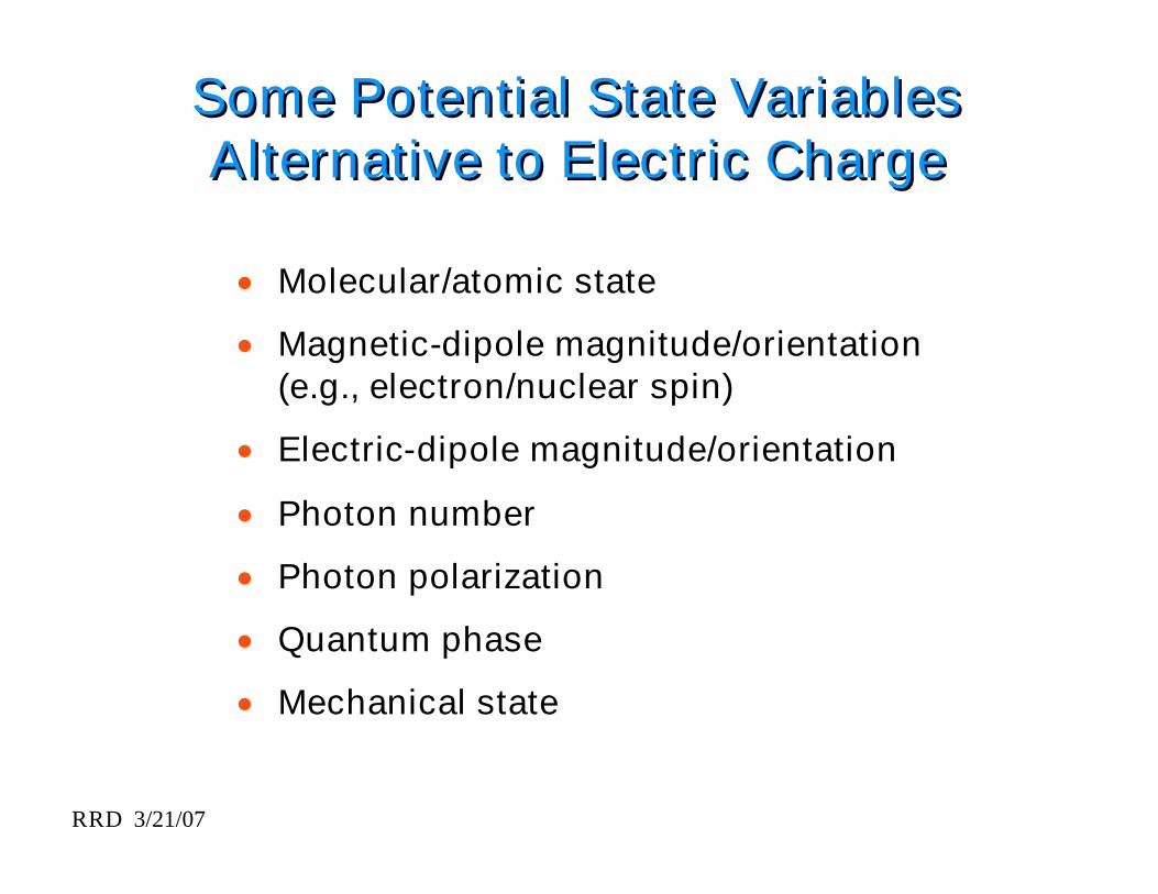
Some Potential State VariablesAlternative to Electric Charge
Some Potential State VariablesAlternative to Electric Charge
Molecular/atomic state
Magnetic-dipole magnitude/orientation(e.g., electron/nuclear spin)
Electric-dipole magnitude/orientation
Photon number
Photon polarization
Quantum phase
Mechanical state
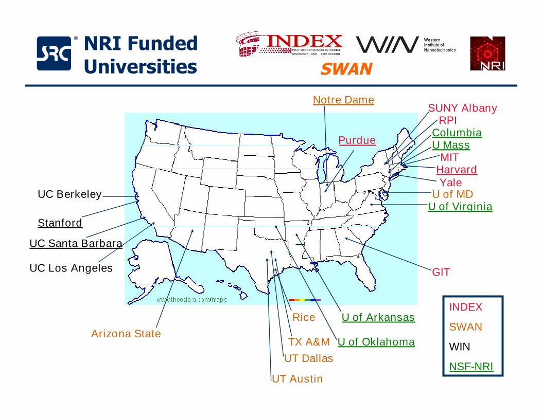
NRI FundedUniversities
SUNY Albany
U of Virginia
GIT
Columbia
Harvard
Purdue
U of Arkansas
U MassMIT
U of OklahomaArizona State
Rice
TX A&MUT Dallas
UT Austin
U of MD
Notre Dame
UC Berkeley
UC Los Angeles
Stanford
UC Santa Barbara
INDEX
SWAN
WIN
NSF-NRI
RPI
Yale
INSTITUTE FOR NANOELECTRONICSINSTITUTE FOR NANOELECTRONICS
DISCOVERY AND EXPLORATIONDISCOVERY AND EXPLORATION
INSTITUTE FOR NANOELECTRONICSINSTITUTE FOR NANOELECTRONICS
DISCOVERY AND EXPLORATIONDISCOVERY AND EXPLORATION
SWAN
RRD 3/21/07
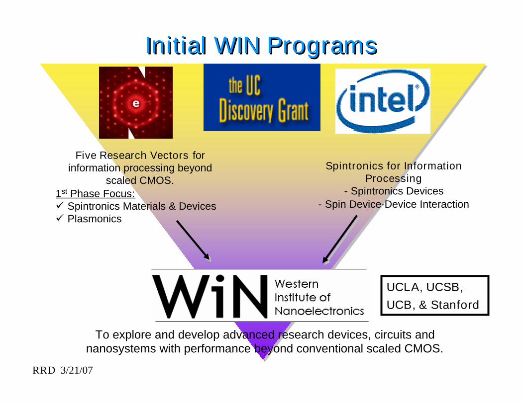
Initial WIN ProgramsInitial WIN Programs
To explore and develop advanced research devices, circuits andnanosystems with performance beyond conventional scaled CMOS.
Five Research Vectors forinformation processing beyond
scaled CMOS.1st Phase Focus:Spintronics Materials & DevicesPlasmonics
Spintronics for InformationProcessing
- Spintronics Devices- Spin Device-Device Interaction
UCLA, UCSB,UCB, & Stanford
RRD 3/21/07
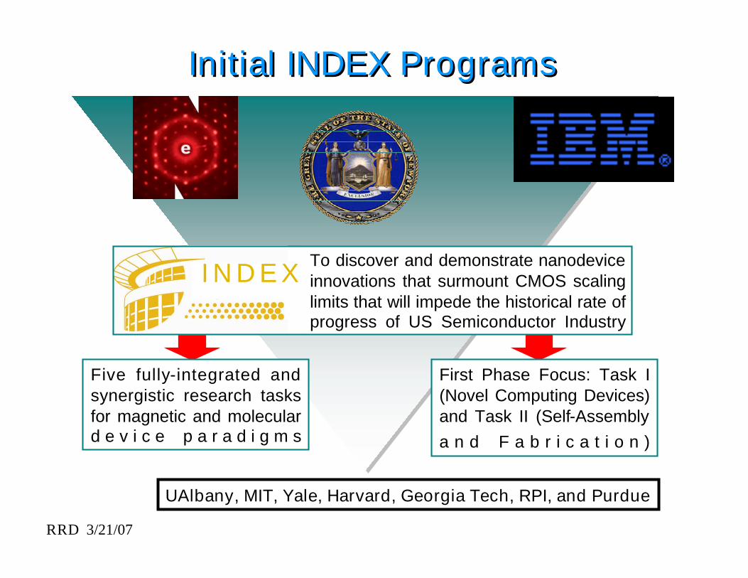
Five fully-integrated andsynergistic research tasksfor magnetic and moleculard e v i c e p a r a d i g m s
To discover and demonstrate nanodeviceinnovations that surmount CMOS scalinglimits that will impede the historical rate ofprogress of US Semiconductor Industry
I N D E X
First Phase Focus: Task I(Novel Computing Devices)and Task II (Self-Assemblya n d F a b r i c a t i o n )
Initial INDEX ProgramsInitial INDEX Programs
UAlbany, MIT, Yale, Harvard, Georgia Tech, RPI, and Purdue
RRD 3/21/07
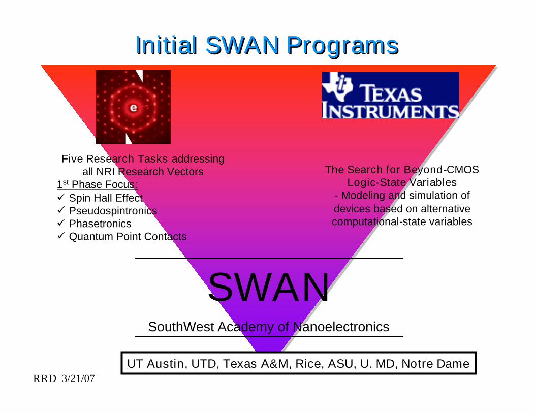
Five Research Tasks addressingall NRI Research Vectors
1st Phase Focus:Spin Hall EffectPseudospintronicsPhasetronicsQuantum Point Contacts
The Search for Beyond-CMOSLogic-State Variables
- Modeling and simulation ofdevices based on alternativecomputational-state variables
Initial SWAN ProgramsInitial SWAN Programs
SWANSouthWest Academy of Nanoelectronics
UT Austin, UTD, Texas A&M, Rice, ASU, U. MD, Notre Dame
SWAN
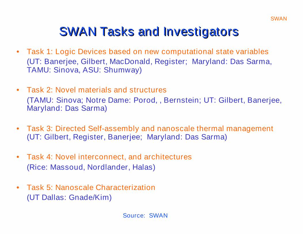
SWAN Tasks and InvestigatorsSWAN Tasks and Investigators
• Task 1: Logic Devices based on new computational state variables(UT: Banerjee, Gilbert, MacDonald, Register; Maryland: Das Sarma,TAMU: Sinova, ASU: Shumway)
• Task 2: Novel materials and structures(TAMU: Sinova; Notre Dame: Porod, , Bernstein; UT: Gilbert, Banerjee,Maryland: Das Sarma)
• Task 3: Directed Self-assembly and nanoscale thermal management(UT: Gilbert, Register, Banerjee; Maryland: Das Sarma)
• Task 4: Novel interconnect, and architectures(Rice: Massoud, Nordlander, Halas)
• Task 5: Nanoscale Characterization(UT Dallas: Gnade/Kim)
Source: SWAN
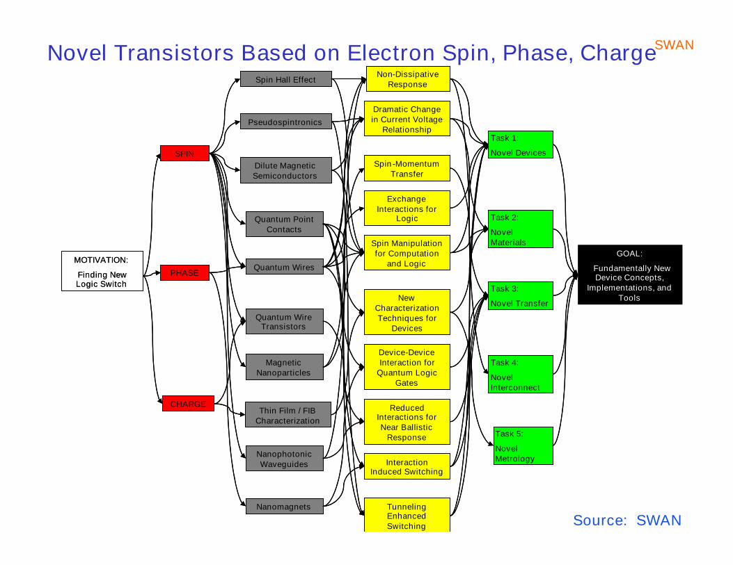
SWANNovel Transistors Based on Electron Spin, Phase, ChargeSpin Hall Effect
Pseudospintronics
MagneticNanoparticles
Quantum PointContacts
Quantum Wires
TunnelingEnhancedSwitching
MOTIVATION:
Finding NewLogic Switch
SPIN
PHASE
CHARGE ReducedInteractions forNear Ballistic
Response
Device-DeviceInteraction for
Quantum LogicGates
GOAL:
Fundamentally NewDevice Concepts,
Implementations, andTools
Quantum WireTransistors
Non-DissipativeResponse
Dramatic Changein Current Voltage
Relationship
Spin-MomentumTransfer
Spin Manipulationfor Computation
and Logic
Nanomagnets
NanophotonicWaveguides
Thin Film / FIBCharacterization
Task 1:
Novel Devices
Task 2:
NovelMaterials
Task 3:
Novel Transfer
Task 4:
NovelInterconnect
Task 5:
NovelMetrology
Dilute MagneticSemiconductors
InteractionInduced Switching
NewCharacterizationTechniques for
Devices
ExchangeInteractions for
Logic
Spin Hall Effect
Pseudospintronics
MagneticNanoparticles
Quantum PointContacts
Quantum Wires
TunnelingEnhancedSwitching
MOTIVATION:
Finding NewLogic Switch
SPIN
PHASE
CHARGE ReducedInteractions forNear Ballistic
Response
Device-DeviceInteraction for
Quantum LogicGates
GOAL:
Fundamentally NewDevice Concepts,
Implementations, andTools
Quantum WireTransistors
Non-DissipativeResponse
Dramatic Changein Current Voltage
Relationship
Spin-MomentumTransfer
Spin Manipulationfor Computation
and Logic
Nanomagnets
NanophotonicWaveguides
Thin Film / FIBCharacterization
Task 1:
Novel Devices
Task 2:
NovelMaterials
Task 3:
Novel Transfer
Task 4:
NovelInterconnect
Task 5:
NovelMetrology
Dilute MagneticSemiconductors
InteractionInduced Switching
NewCharacterizationTechniques for
Devices
ExchangeInteractions for
Logic
Source: SWAN
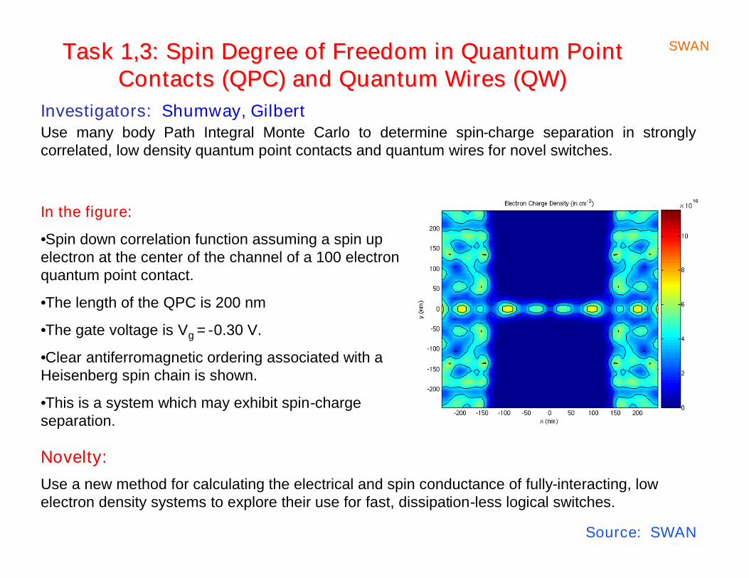
SWANTask 1,3: Spin Degree of Freedom in Quantum PointTask 1,3: Spin Degree of Freedom in Quantum PointContacts (QPC) and Quantum Wires (QW)Contacts (QPC) and Quantum Wires (QW)
Investigators:Investigators: Shumway, Gilbert
Novelty:Novelty:
Use a new method for calculating the electrical and spin conductance of fully-interacting, lowelectron density systems to explore their use for fast, dissipation-less logical switches.
Use many body Path Integral Monte Carlo to determine spin-charge separation in stronglycorrelated, low density quantum point contacts and quantum wires for novel switches.
In the figure:In the figure:
•Spin down correlation function assuming a spin upelectron at the center of the channel of a 100 electronquantum point contact.
•The length of the QPC is 200 nm
•The gate voltage is Vg = -0.30 V.
•Clear antiferromagnetic ordering associated with aHeisenberg spin chain is shown.
•This is a system which may exhibit spin-chargeseparation.
Source: SWAN
SWAN
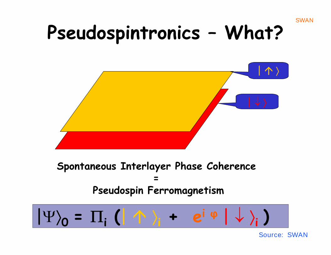
Pseudospintronics – What?
|
|
|0 = i (| i + ei φ| i )
Spontaneous Interlayer Phase Coherence=
Pseudospin Ferromagnetism
Source: SWAN
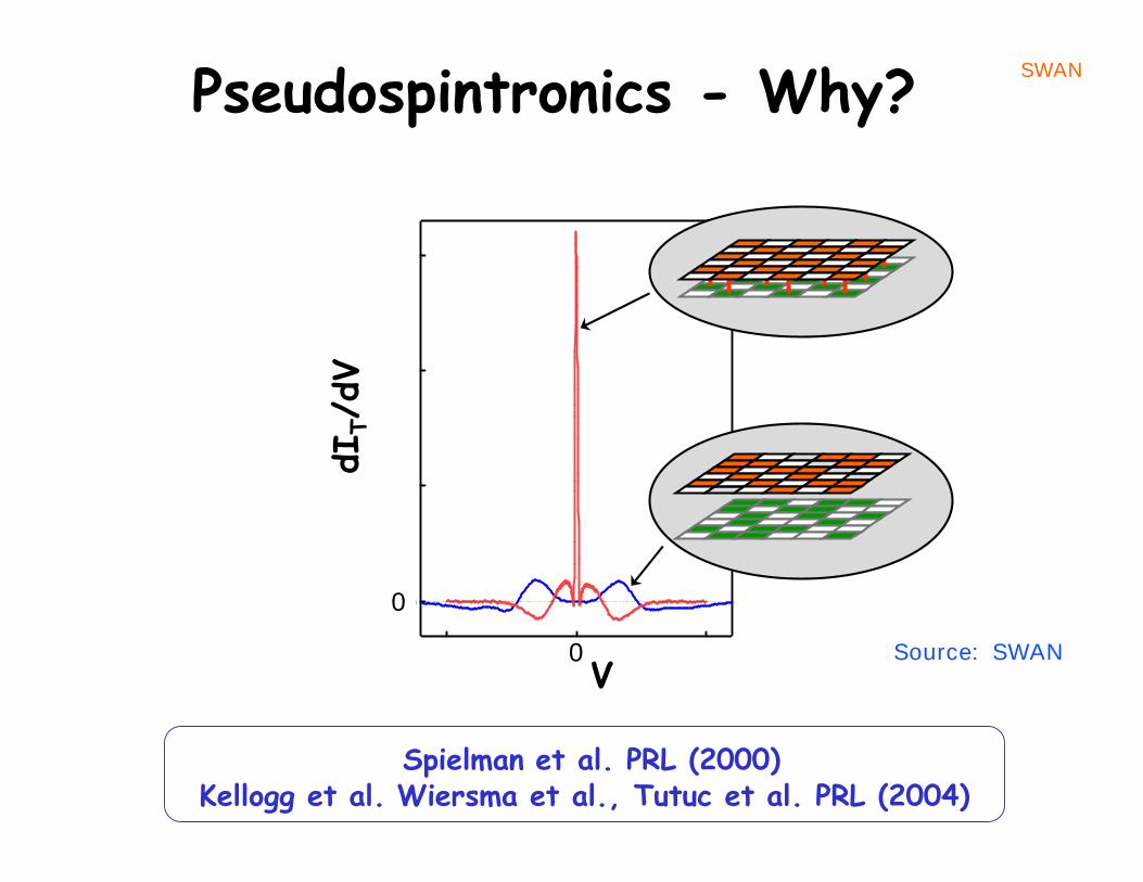
SWANPseudospintronics - Why?
Spielman et al. PRL (2000)Kellogg et al. Wiersma et al., Tutuc et al. PRL (2004)
300
200
100
0Tun
nelin
gC
ondu
ctan
ce(1
0-9
-1)
-5 0 5Interlayer Voltage (mV)
0
dIT/d
V
0
VSource: SWAN
SWAN
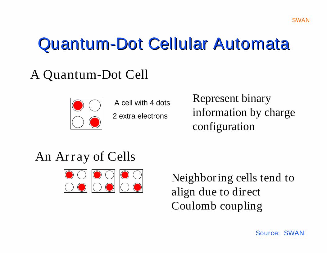
Quantum-Dot Cellular AutomataQuantum-Dot Cellular Automata
Represent binaryinformation by chargeconfiguration
A cell with 4 dots
2 extra electrons
Neighboring cells tend toalign due to directCoulomb coupling
A Quantum-Dot Cell
An Array of Cells
Source: SWAN
SWAN
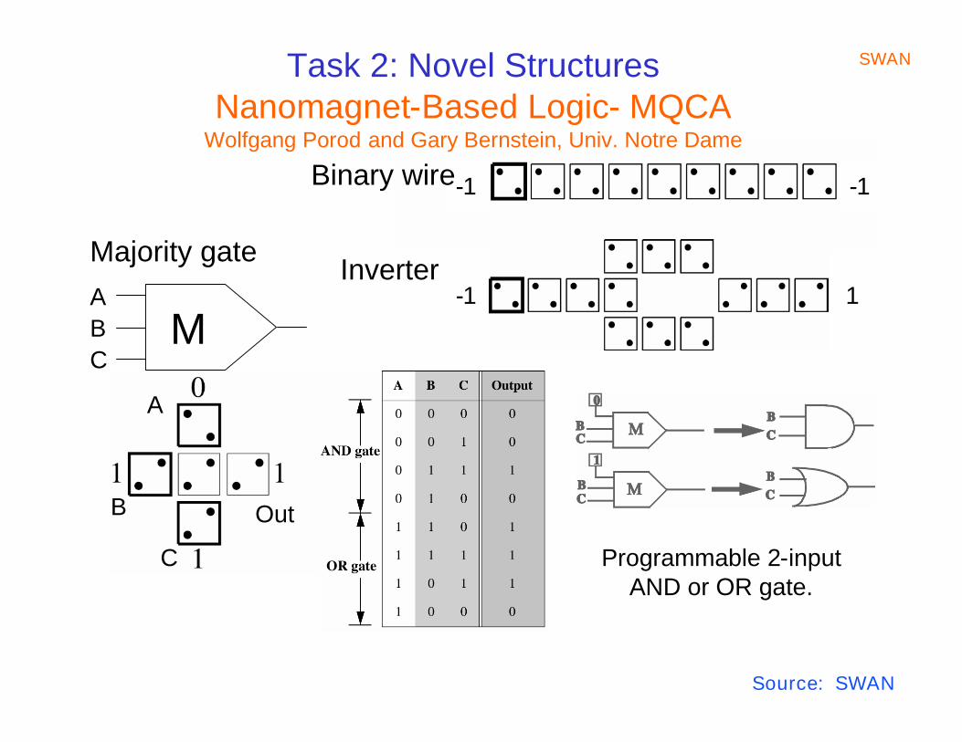
1 1-1 -1
A
B
C
Out
-11 1-1
Binary wire
InverterMajority gate
MABC
Programmable 2-inputAND or OR gate.
Task 2: Novel StructuresNanomagnet-Based Logic- MQCA
Wolfgang Porod and Gary Bernstein, Univ. Notre Dame
Source: SWAN
SWAN
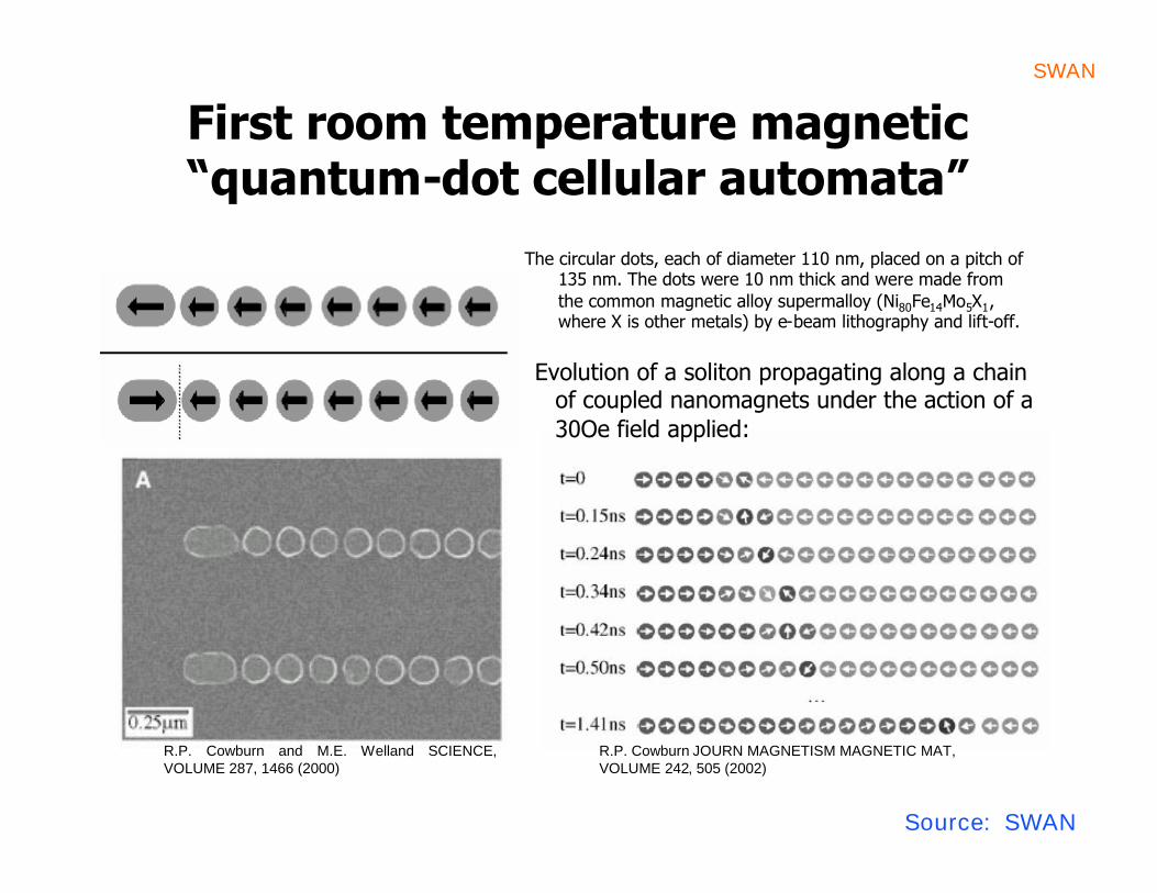
First room temperature magnetic“quantum-dot cellular automata”
R.P. Cowburn and M.E. Welland SCIENCE,VOLUME 287, 1466 (2000)
R.P. Cowburn JOURN MAGNETISM MAGNETIC MAT,VOLUME 242, 505 (2002)
Evolution of a soliton propagating along a chainof coupled nanomagnets under the action of a30Oe field applied:
The circular dots, each of diameter 110 nm, placed on a pitch of135 nm. The dots were 10 nm thick and were made fromthe common magnetic alloy supermalloy (Ni80Fe14Mo5X1,where X is other metals) by e-beam lithography and lift-off.
Source: SWAN
SWAN
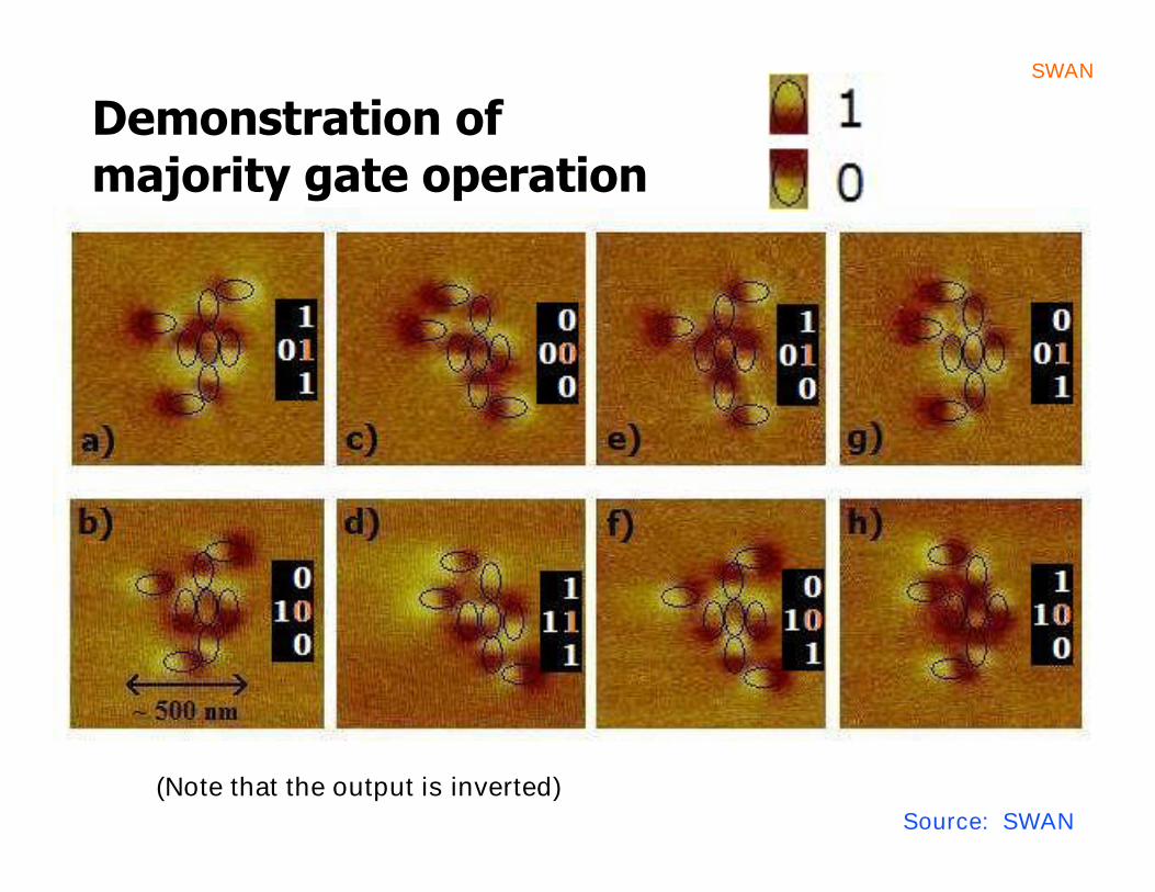
Demonstration ofmajority gate operation
(Note that the output is inverted)Source: SWAN
RRD 3/21/07
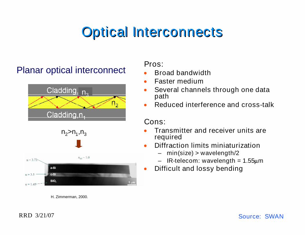
Optical InterconnectsOptical Interconnects
Planar optical interconnectPros: Broad bandwidth Faster medium Several channels through one data
path Reduced interference and cross-talk
Cons: Transmitter and receiver units are
required Diffraction limits miniaturization
– min(size) > wavelength/2– IR-telecom: wavelength = 1.55m
Difficult and lossy bending
n3
n2>n1,n3
H. Zimmerman, 2000.
Source: SWAN
RRD 3/21/07
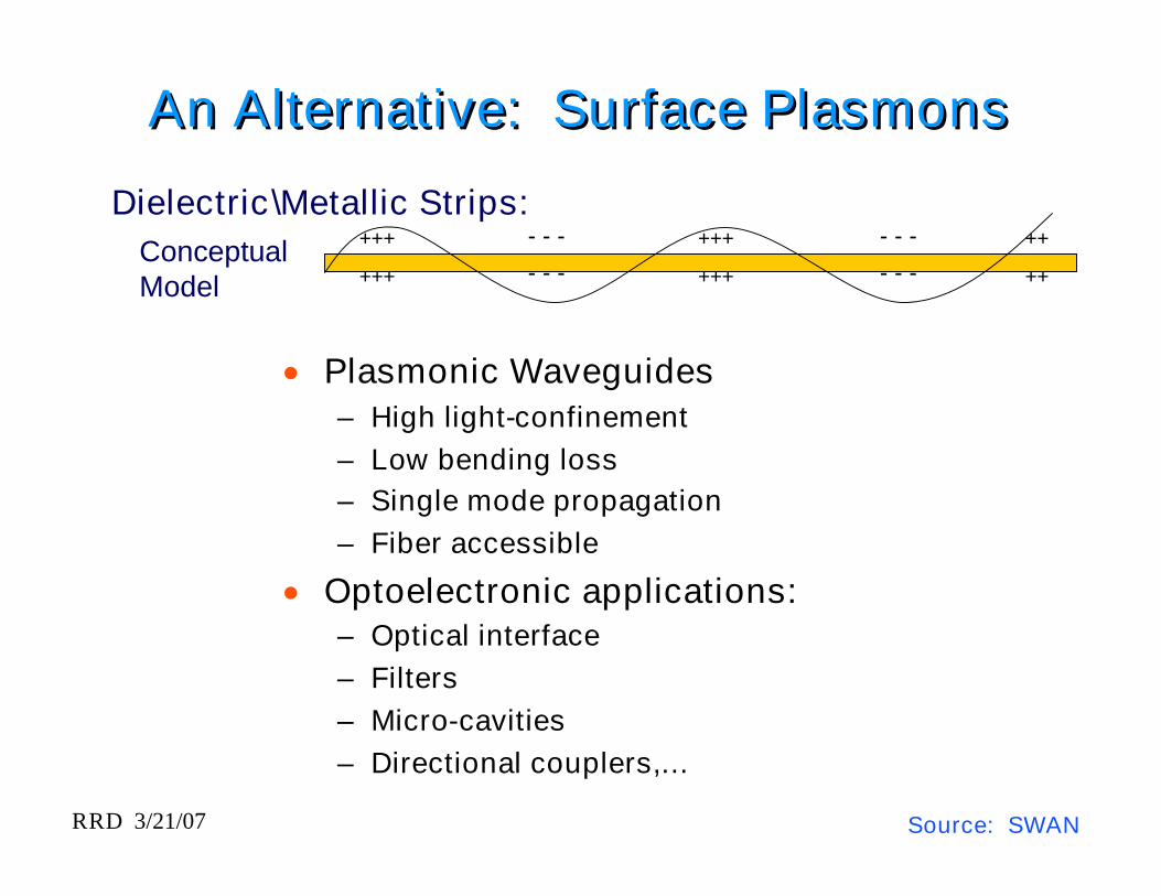
An Alternative: Surface PlasmonsAn Alternative: Surface Plasmons
Plasmonic Waveguides– High light-confinement– Low bending loss– Single mode propagation– Fiber accessible
Optoelectronic applications:– Optical interface– Filters– Micro-cavities– Directional couplers,…
Dielectric\Metallic Strips:+++ +++ ++
- - -
- - -
+++ +++
- - -
- - - ++ConceptualModel
Source: SWAN
RRD 3/21/07
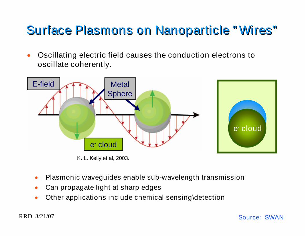
Oscillating electric field causes the conduction electrons tooscillate coherently.
Surface Plasmons on Nanoparticle “Wires”Surface Plasmons on Nanoparticle “Wires”
K. L. Kelly et al, 2003.
E-field
e- cloud
MetalSphere
e- cloud
Plasmonic waveguides enable sub-wavelength transmission Can propagate light at sharp edges Other applications include chemical sensing\detection
Source: SWAN
RRD 3/21/07
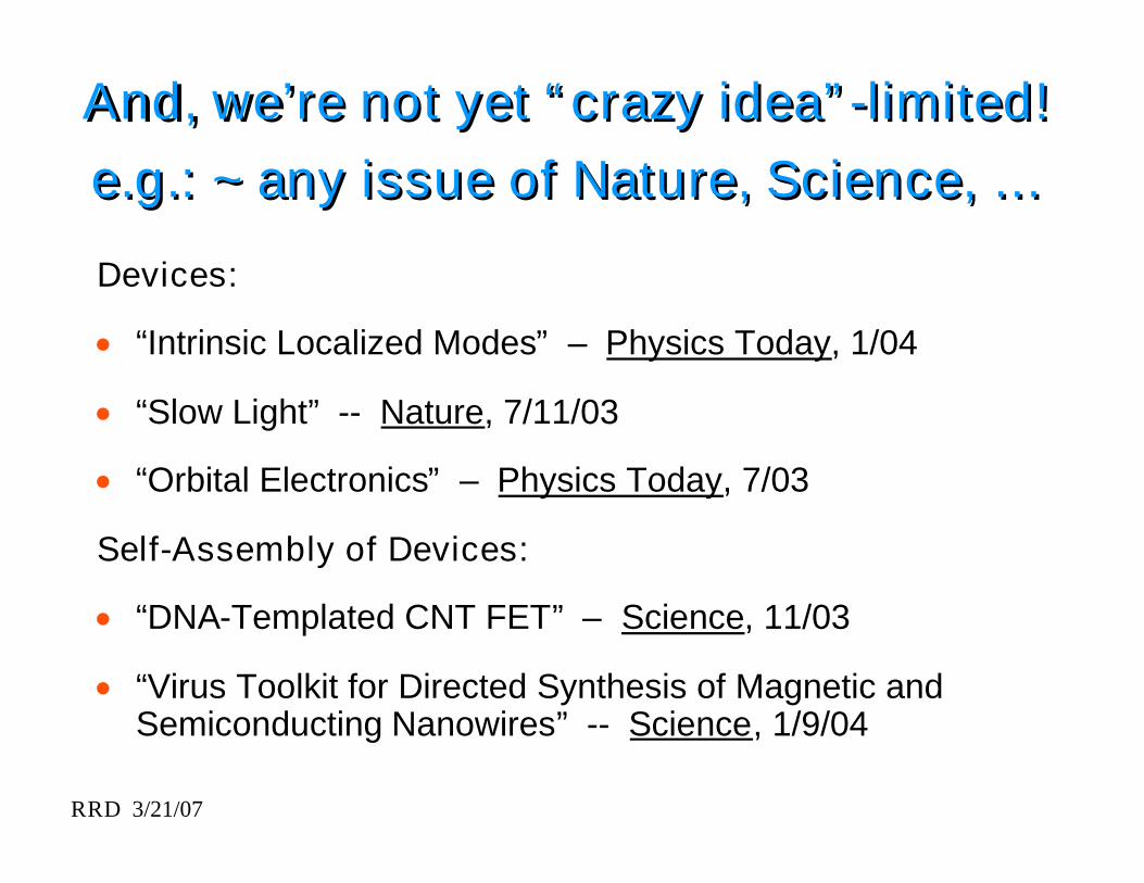
Devices:
“Intrinsic Localized Modes” – Physics Today, 1/04
“Slow Light” -- Nature, 7/11/03
“Orbital Electronics” – Physics Today, 7/03
Self-Assembly of Devices:
“DNA-Templated CNT FET” – Science, 11/03
“Virus Toolkit for Directed Synthesis of Magnetic andSemiconducting Nanowires” -- Science, 1/9/04
And, we’re not yet “crazy idea”-limited!e.g.: ~ any issue of Nature, Science, …
And, we’re not yet “crazy idea”-limited!e.g.: ~ any issue of Nature, Science, …