resonance damping in a higher order filter (lcl) in an active front end operation · 2013-04-04 ·...
TRANSCRIPT

Resonance Damping in a Higher Order Filter (LCL) in an Active Front End
Operation
A Project Report
Submitted for partial fulfillment of degree Master of Engineering
In Electrical Engineering
By
NILANJAN MUKHERJEE
June 2009


i Acknowledgements I express my profound gratitude to my guide Dr. Vinod John for suggesting me the topic and I wish to thank him for giving me opportunity to work with such a fascinating project of current interest. I am again thanking him for providing the course “Dynamics of Linear System” that helped me a lot in my present work and also for providing me freedom that I have enjoyed throughout my work. I cannot forget those ours long discussion with him about the various things related to power electronics. He was really active in discussion with me in each and every problem that I have faced in my work. I sincerely thank Dr. G. Narayanan for his course “PWM Power converter and its application” that helped me to expose such fascinating research area. I am also grateful to him for provided me an opportunity to deal with a highly prospectus mini-project related to my main work that nobody has touched so far. I am grateful to Prof. V.T. Ranganathan, Prof. V. Ramanarayanan for their courses namely, “Electric Drives”, “Switch Mode Power Conversion” as those courses also helped me in my project. I consider myself fortunate to be a part of this Power Electronics Group. I have extreme gratitude & affection for this institute, as I have received every opportunity for self-improvement. I gratefully acknowledge the financial support from the institute for being a Master student. I have all along been enjoying the company of a very good set of friends and seniors here at PEG, especially Dipankar who was there with me all the time as a friend and sometime like an elder brother with all the happenings in these two years. I cherish the wonderful time I have had with him that I cannot forget in my life. It was a great pleasure working with Anirban in the same lab. I got a lot of advice with the discussion with him in the lab. Over all it was a great pleasure to work with this Power Electronics Group. I also had a great time with all my friends here at IISc. I thank Mrs. Silvi Jose for her help in purchase of components etc. I sincerely thank Mr. D.M.Channe Gowda and his colleagues at the EE Office who have always been very helpful.

ii Acknowledgements
Abstract The use of Distributed or Disperse Generation is rapidly increasing in the modern distribution networks because of their potential advantages. They need DC/AC converter in order to interface to the grid .These type of active rectifiers/inverters are used more frequently in regenerative systems and distributed power systems . The switching frequency of these converters is generally between 5 kHz and 20 kHz and causes high order harmonics that can disturb other EMI sensitive loads/equipment on the grid side. Choosing a high value for the line-side inductance can solve this problem, but this makes the system expensive and bulky. On the contrary, to adopt an LCL- filter configuration allows to use reduced values of the inductances (preserving dynamic performance) and to reduce the switching frequency pollution emitted in the grid. The main goal is to ensure a reduction of the switching frequency ripple at a reasonable cost and, at the same time, to obtain a high performance active rectifier. Usually the converter side reactor is bigger than the grid side one because it is responsible for the attenuation of most of the switching ripple. The ac capacitor is limited in order not to reduce too much the reactive power drawn and the grid side reactor is chosen in order to properly tune the cut-off frequency of the LCL-filter. As a drawback these LCL filters have very high gain at the filter cutoff frequency, so naturally if that frequency get excited then system will oscillate. As a result system becomes highly sensitive to outside disturbances. One way of reducing the resonance oscillation in current & voltage of the system is by adding a passive damping circuit to the filter. This damping circuit can be purely resistive or more complex solution consisting of a combination of resistors, capacitors and inductors. A more attractive option is the use of active damping where the output voltage from the converter is used (suitable control action) to damp out the resonance oscillations. The greater emphasis is given to active damping in current work. Some of the techniques are available in the literature based on current control strategy of the converter. But in the current work state-space based method of control is adopted in order to get more flexibility & optimized the energy during control action.

iv Abstract

Contents Acknowledgements i Abstract iii List of Figures ix Nomenclature xiii 1. Introduction …………………………………………………….1
1.1 Organization of the project ………………………………….2
2. Active Front End Operation with LCL filter and Problem of Resonance
2.1 Introduction …………………………………………………3 2.2 Active Front End Converter (AFEC) ……………………….4 2.3 Grid connected operation with “L” filter………………. …..5 2.4 Grid connected operation with “LCL” filter………………...5 2.5 Problem of resonance AFEC …………………………...…..6 2.6 Conclusion ………………………………………………….7
3. Introduction to passive damping in LCL filter
3.1 Introduction ………………………………………………. 9 3.2 Different passive damping topologies……………………..10
3.2.1 Solution 1 ……………………………………… … 10 3.2.2 Solution 2. ………………………………………….13 3.2.3 Solution 3 …………………………………………..14
3.3 Conclusion ………………………………………………..19
4. Introduction to Active damping
4.1 Introduction …………………………………………………20 4.2 Active damping based on traditional approach ……………..20

vi Contents 4.3 Active damping by means of State-space based method ……21 4.4 Filter modeling in state-space ……………………………….21 4.5 Pole-placement of the system ……………………………….22 4.6 Physical realization of Active Damping (Concepts of Virtual resistance) ……………………………..26 4.7 Active damping loop realization …………………………….28 4.8 Conclusion ………………………………………………….29
5. Grid synchronization & Introduction to Phase Locked Loop
5.1 Introduction ………………………………………………….30 5.2 PLL algorithm ……………………………………………...30 5.3 Conclusion …………………………………………………..34
6. Control Scheme for Standalone and Grid Interactive Mode with LCL Filter
6.1 Introduction …………………………………………………..36 6.2 Model for control design ……………………………………..36 6.3 Over view of the control loop consisting of three states of the
system …………………………………………………………39 6.4 Current control strategy ……………………………...……….41 6.5 Analysis of controller performance... ………………………...43 6.6 Inclusion of inner most state-space based damping loop ….;...46 6.7 Operation in standalone mode with LCL filter………………..47 6.8 Control in standalone mode with LCL filter
…………………………………………………………………48 6.9 Sensor less operation..…………..…..………………………..49 6.10 Conclusion ...……………………….……………..…………50
7. Simulation Results
7.1 Introduction ………………………………………………….52 7.2 System parameters …………………………………………...52 7.3 Standalone mode results ……………………………………..53

Contents vii 7.4 Grid connected mode results ……………………………...53 7.5 Conclusion ………………………………………………...66
8. Experimental Results
8.1 Introduction …………………………………………………..68 8.2 Standalone Mode of operation ………………………………..68 8.3 grid connected mode of operation ……………………………74 8.4 Conclusion …………………………………………………....79
A. Further Investigation about damping
A.1 Introduction ………………………………………………….81 A.2 Comparison of Active & Passive damping ………………….81 A.3 Optimal damping (Advanced Active Damping) …………….83 A.3.1 Introduction …………………………………………..…83 A.3.2 Optimal gain matrix calculation …………………………83
A.4 Conclusion …………………………………………………86
B. Hardware Implementation
B.1 Introduction …………………………………………………..87 B.2 Experimental Setup …………………………………………..87 B.2.1 Diode bridge rectifier …………………………………...87 B.2.2 Pre-charging Autotransformer ………………………….89 B.2.3 IGBT based inverter ……………………………………89 B.2.4 FPGA Controller ……………………………………….89 B.3 Implementation stages………………………………………..92 B.4 Conclusion …………………………………………………...92
References ………………………………………………………….…...94

viii contents

List of Figures 2.1 Grid connected operation with the simple “L” filter ……………...5 2.2 Grid connected operation with the third order “LCL” filter ……....5 2.3 PWM waveform applied to the filter ………………………….......6 2.4 LCL filter is being excited by unit impulse …………………….....7 3.1 frequency response of the capacitor current in LCL filter …….….11 3.2 series damping in LCL filter ………………………………….…..11 3.3 Frequency response of capacitor current after damping ……….…12 3.4 bypassing the damping resistance by fL ………………………....13 3.5 Frequency response with bypassing inductance ……………….…14 3.6 R-C parallel damping for the LCL filter ………………………...14 3.7 damping by changing fC / C ratio ………………………………...15
3.8 Root locus analysis of L2
inv
iU
transfer function in damped case ….....16
3.9 change of closed loop poles with the variation of ‘a ……….…….16 3.10 Comparison of transient response with different ‘a’……….……17 3.11 Variation of ‘Q’ with the ‘a’……………………………….……17 3.12 overall comparison of Loss, attenuation, Damping with fC / C ratio …………………………………..…….….18 4.1 Typical scheme for Active damping …………………….……….23 4.2 Pole placement to LHS of s-plane ………………………….…….23 4.3 Active damping by weight age capacitor current feedback ….…...25 4.4 Approximate Circuit representation for Active damping …….…...26 4.5 comparison of different damping factor in Active Damping ….…..27 4.6 State-space based active damping loop (general case) …………....28 4.7 Comparison of virtual resistance based damping & actual resistance based damping of L2
inv
iU
transfer function……………………………….29
5.1 Basic PLL structure …………………………………………….30 5.2 Reference frame ……………………………………………………31 5.3 Simplified block diagram of SRF PLL …………………………..33 5.4 Theta is synchronized with grid voltage …………………………...33 5.5 sin( )θ and 'sin( )θ synchronized with each other …………………39 6.1 Active rectifier with LCL filter ……………………………………..37 6.2 Grid connection with LCL filter ……………………………………37 6.3 Conventional three loop control strategy for LCL filter ……………39

x List of Figures 6.4 Two loop control strategy for LCL filter ……………………………40 6.5 Single loop control strategy for LCL filter ………………………….41 6.6 Modified two loop control strategy for LCL filter ………………….42 6.7 Two loop control strategy for LCL filter ……………………………42
6.8 Root locus of *
L2
L2
ii
with pK = 0.5 ……………………………………43
6.9 Root locus of *
L2
L2
ii
with pK = 1 ………………………………………44
6.10 Root locus of *
L2
L2
ii
with pK = 2 ……………………………………..44
6.11 Bode plot of *
L2
L2
ii
with different value of Kc ………………………45
6.12 Current control with State-space based damping loop …………….46 6.13 Standalone mode of operation ……………………………………..47 6.14 Vector control of standalone mode ………………………………..48 6.15 Vector control in grid parallel mode ………………………………49 7.1 d-axis load side current in standalone when the reference changes @ 0.05 sec ………………………………………………………………….55 7.2 q-axis load side current in standalone when the reference changes @ 0.05 sec …………………………………………………………………55 7.3 R-phase load side current in standalone when the reference changes @ 0.05 sec………………………………………………………………….56 7.4 capacitor current in standalone when the reference changes @ 0.05 sec……………………………………………………………….56 7.5 Capacitor voltage in standalone when the reference changes @ 0.05 sec ………………………………………………………………57 7.6 d-axis load side current in standalone when the damping loop is being enabled @ 0.02 sec ……………………………………………………..57 7.7 q-axis load side current in standalone when the damping loop is being enabled @ 0.02 sec …………………………………………………….58 7.8 Capacitor current in standalone when the damping loop is being enabled @ 0.02 sec………………………………………………………………58 7.9 Capacitor voltage in standalone when the damping loop is being enabled @ 0.02 sec………………………………………………………………59 7.10 R-phase load side current in standalone when the damping loop is being enabled @ 0.02 sec ……………………………………………………..59
List of Figures xi 7.11 d-axis grid side current in no-load where the reactive power reference changes @ 0.02 sec …………………………………………………….60 7.12 q-axis grid side current in no-load ………………………………..60 7.13 grid side current in no-load …………………………………….. 7.14 DC-link voltage profile in no load ……………………………….61 7.15 Fundamental of R-phase inverter voltage& grid voltage of R-phase ………………………………………………..61 7.16 d-axis current of grid side with load ……………………………..62 7.17 q-axis current of grid side with load enabled @ 0.08sec ………...62 7.18 line side current of R-phase with load enabled @ 0.08sec ………63 7.19 DC-link voltage profile when the load is being enabled @ 1.5sec..63 7.20 Line side current & line voltage with UPF operation ……………64 7.21 Line side current when active damping enabled @ 0.1 sec ………64 7.22 capacitor voltage when active damping enabled @ 0.1 sec ………65 7.23 capacitor current when active damping enabled @ 0.1 sec ………66 8.1 q-axis load side current with change of reference ………………….69 8.2 q-axis load side current with change of reference ………………….69 8.3 load side current with change of reference …………………………70 8.4 Un-damped load current & its spectra in standalone mode …………70 8.5 Damped load current & its spectra in standalone mode …………….71 8.6 Active damping test of load current with lesser state-weight age …..71 8.7 Active damping test of load current with higher state-weight age ….72 8.8 Un-damped capacitor current & its spectra …………………………72 8.9 Active damping test of capacitor current ……………………………73 8.10 Active damping test of q-axis capacitor current ……………………73 8.11 DC – bus control test (voltage rise)…………………………………74 8.12 DC – bus control test (voltage falling)……………………………...74 8.13 Distorted current from grid (full of resonance)……………………..75 8.14 Less distorted current grid (state-weight age K=10)………………...75 8.15 smooth current from grid (state-weight age 25) and its FFT………..76 8.16 grid side current dynamics when sudden change in DC-bus………..76 8.17 grid side current dynamics when sudden change load ……………...77 8.18 Line side current when active damping is being enabled mid-way…77 8.19 Active damping loop is being enabled mid-way with BW of 1.2 KHz………………………………………………………………………78 8.20 Distortion in the utility voltage and smoothing out by active damping…………………………………………………………………..78
xii List of Figures
A.1 Frequency response of 1L
inv
iU for un-damped, actively damped &
passively damped system…………………………………………………82
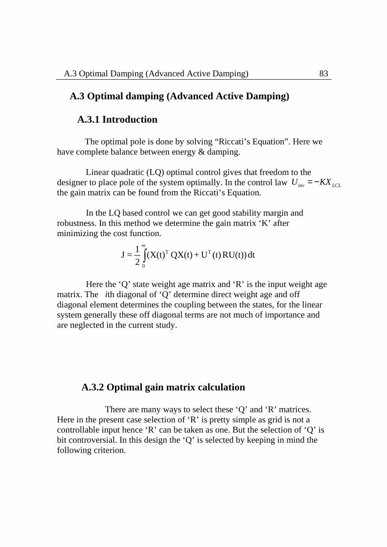
A.2 Frequency response of 2L
inv
iU for un-damped, actively damped &
passively damped system…………………………………………………82 A.3 Root loci of the original system & optimally damped system ………85
A.4 Frequency response of 1L
inv
iU in the original system & optimally damped
system…………………………………………………………………….85
A.5 Frequency response of 2L
inv
iU in the original system & optimally damped
system……………………………………………………………………86 B.1 Complete Hardware Setup ………………………………………….88 B.2 Block diagram of the FPGA board …………………………………90
Nomenclatures Symbols Definition
dcV : DC-bus voltage.
invU : Inverter output voltage.
gU : Grid voltage
cV : Capacitor voltage in LCL filter
Q : Quality factor / state weight age matrix
rw : Resonance frequency in rad/s
LCLA : System matrix in LCL filter
LCLB : Input matrix in LCL filter
LCLC : Output matrix in LCL filter
LCLX : State vector
ξ : Damping ratio
L1i : Inverter side current
L2i : Grid side current/line side current
ic : Capacitor current in LCL filter
dR : Damping resistance in LCL filter
fL : Bypassing inductance in damping circuit
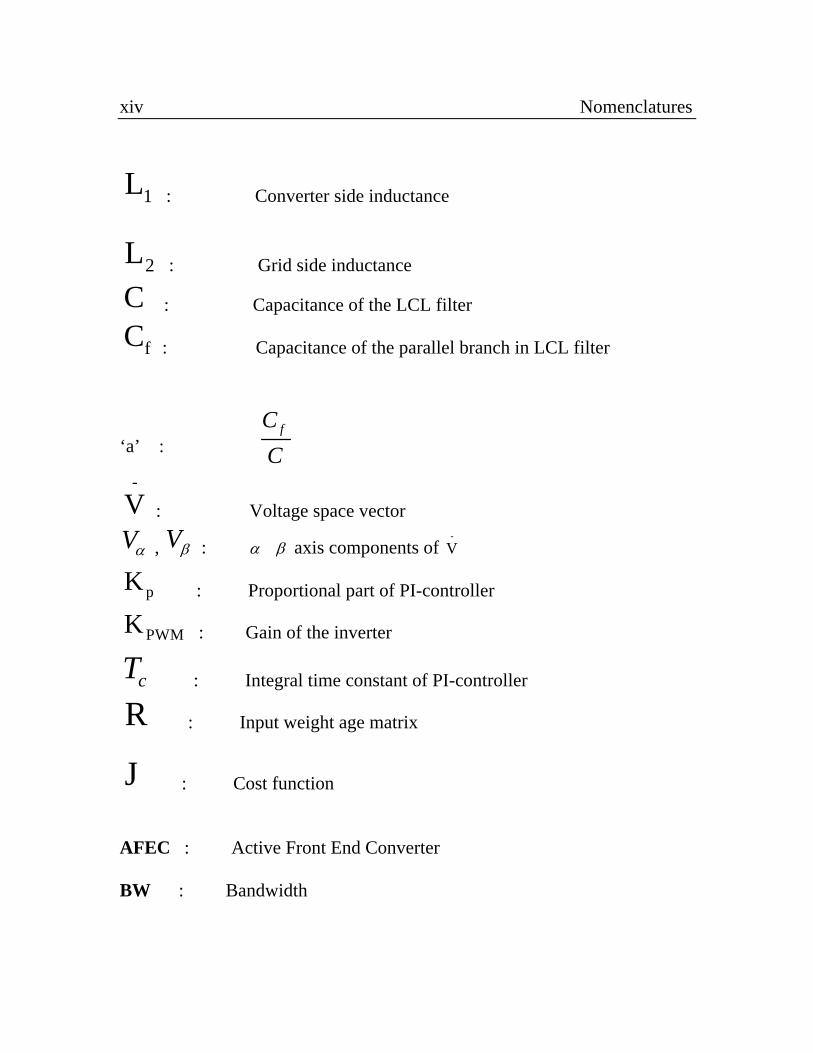
xiv Nomenclatures
1L : Converter side inductance
2L : Grid side inductance
C : Capacitance of the LCL filter
fC : Capacitance of the parallel branch in LCL filter
‘a’ : fC
C
-V : Voltage space vector
Vα , Vβ : α β axis components of -
V
pK : Proportional part of PI-controller
PWMK : Gain of the inverter
cT : Integral time constant of PI-controller
R : Input weight age matrix
J : Cost function AFEC : Active Front End Converter BW : Bandwidth
Chapter 1 Introduction Three-phase grid connected PWM rectifiers (Active rectifier) are often used in regenerative system & adjustable drives system when regenerative braking is required. Apart from power generation, they offer control of power factor as well as dc link voltage while injecting lower current harmonics to the grid than passive diode rectifier bridges. Traditionally, LC filter is used for an inverter power supply like in UPS system. A grid-interconnected inverter used in such an application however, has some unique requirements that an LC filter may not be sufficient. (Based on IEEE 519-1992) A PWM converter with higher switching frequency will result in smaller LC filter size. However, switching frequency is generally limited in high power applications. As an alternative solution, LCL filter is more attractive for two reasons: First, they offer advantages in terms of costs & dynamics second; it has better attenuation than LC filter given the size. LCL filter also provides inductive output at the grid interconnection point to prevent inrush current compared to LC filter. One drawback LCL filter based Active rectifier system is that the filter can oscillate with the resonance frequency. Active damping is generally more attractive than passive damping as of it is being loss-less & more flexible however, the control bandwidth is quite limited in high power converters due to their limitation in switching frequency. Here in the present work the design part of the filter is not considered. Concentration is given to the damping part of LCL filter. First part of the work is concentrated on the passive damping & the next part is focused on active damping.

2 Chapter 1. Introduction 1.1 Organization of the report Chapter 2: Active front end operation with LCL filter and problem of LCL resonance. Chapter 3: Introduction to passive damping in LCL filter Chapter 4: Introduction to Active damping Chapter 5: Grid synchronization & Introduction to Phase Locked Loop Chapter 6: Control Scheme for Standalone and Grid Interactive Mode with LCL Filter Chapter 7: Simulation Results Chapter 8: Experimental results.
Chapter 2 Active Front End Operation with LCL filter and Problem of Resonance 2.1 Introduction Active rectifier / active front end converters have been used in drives as well as distributed generation system & now becoming more and more popular because of its ability to control the line side power factor and load voltage at a time. This type of converters connected between load and the grid /utility in order to supply fine quality of power to the load. Now AFEC can be connected to the grid through “L” filter & “LCL” filter The major advantage of the L type of filter are, design is simple and implementation is bit easy, but at the same time disadvantage of the “L” filter are large magnitude required to provide required attenuation, poor dynamic response due to large time lag . System will be bulky and cost as well as inefficient in application like 100’s of KW or MW range. On the other hand “LC” filter has better attenuation compared to “L” filter but there is always a problem of inrush current due to grid voltage fluctuation. Now “LCL” filter is better than these filters because of giving better decoupling between filter and grid (reducing the dependence on grid parameters.) as well as excellent attenuation of -60dB/decade to the switching frequency harmonics.
4 Chapter 2. Active Front End Operation with LCL filter and Problem of Resonance
2.2 Active Front End Converter (AFEC) The converter consists of a three-phase bridge, a high capacitance on the dc side and a three-phase filter in the line side. The voltage at the mid point of a leg or the pole voltage Vi is pulse width modulated (PWM) in nature. The pole voltage consists of a fundamental component (at line frequency) besides harmonic components around the switching frequency of the converter. Being at high frequencies, these harmonic components are well filtered by the high inductances (L) or some higher order line filter (LCL). Hence the current is near sinusoidal. The fundamental component of Vi controls the flow of real and reactive power. It is well known that the active power flows from the leading voltage to the lagging voltage and the reactive power flows from the higher voltage to the lower voltage. Therefore, controlling the phase and magnitude of the converter voltage fundamental component with respect to the grid voltage can control both active and reactive power. As the grid voltage leads the converter pole voltage, real power flows from the ac side to the dc side, while the reactive power flows from the converter to the grid Apart from control of real and reactive power flow, an FEC should also have a fast dynamic response. Operation of FEC with the first order ‘L’ filter is well reported in the literature but operation of this type active rectifier with ‘LCL’ filter has now started drawing attention [12],[2]. The present work chooses LCL filter based Active Front End converter as its control platform

2.3 Grid connected operation with “L” filter 5 2.3 Grid connected operation with “L” filter
L
R
Y
B
+Vdc/2
+Vdc/2
OL
L
LidcV
Active rectifier
LOAD
dci
Grid
Fig 2.1 Grid connected operation with the simple “L” filter 2.4 Grid connected operation with “LCL” filter
Fig 2.2 Grid connected operation with the third order “LCL” filter
GridGrid
GridC
L1 L2
L2L1
C C
R
Y
B
Neutral
Active Rectifier
O
1Li 2LicV
L1LOAD
dcidcV
Loadi
N
L2

6 Chapter 2. Active Front End Operation with LCL filter And Problem of Resonance
Fig 2.3 PWM waveform applied to the filter 2.5 Problem of LCL resonance in AFEC Normally grid impedance reflected back to the converter side is generally very less so, if the resonance is excited, the oscillation of that can continue for ever and it can make the entire system very vulnerable. Actually when the PWM converter is switched on, the filter (LCL) encounter a sudden pulse at the input as a result filter starts to oscillate in its cutoff frequency. Here is an attempt to show how the resonance is excited by PWM converter (AFEC) itself. For that LCL filter is modeled inside the FPGA based controller & fed from a very narrow single pulse from the same controller. After exciting from the pulse, filter starts to oscillate at resonant frequency. Pulse is being generated in FPGA by means of switch de-bouncing logic
Grid
L1 L2
C
Vc
Simplified Power circuit
1Li 2Li
ciinvU
gU

2.6 Conclusion 7
Fig 2.4 LCL filter is being excited by unit impulse 2.6 Conclusion
In the grid-connected operation with LCL filter, like Distribution Generation case or in Front End operation, damping carries a significant part of designs if we want to utilize the advantages of higher order filter.
There are two ways to damp the resonance, Passive Damping and Active damping. First one can damp resonance in all condition but it is of loss full process & second one can act only when the power converter is switching. Firstly Passive damping is taken to describe & then active damping is analyzed.

8 Chapter 2. Active Front End Operation with LCL filter and Problem of Resonance
Chapter 3 Introduction to passive damping in LCL filter 3.1 Introduction Damping is essential in LCL filter based grid connected system or in the case, when it is connected to light load (standalone mode of operation). This resonance effect can cause instability in the output, especially if some harmonic voltage/current is near the resonant frequency. Damping by control algorithm (Active damping) is most attractive however; the control bandwidth is quite limited in high power converters due to their low switching frequency. Therefore passive damping (by addition of passive circuit elements) is considered in most of the cases. Here in this chapter different passive damping topologies are described & compared. The criteria for the following comparison are effective resonance suppression without deteriorating the attenuation at switching frequency. The Bode plots are used to analyze the performance of damping filters. The five different damping topologies are described. There is always a tradeoff exits between losses & damping in the passive damping, so this also give limitation of passive damping in different cases. Those issues are compared; solution is given depending on power level, damping requirement & efficiency (or losses).
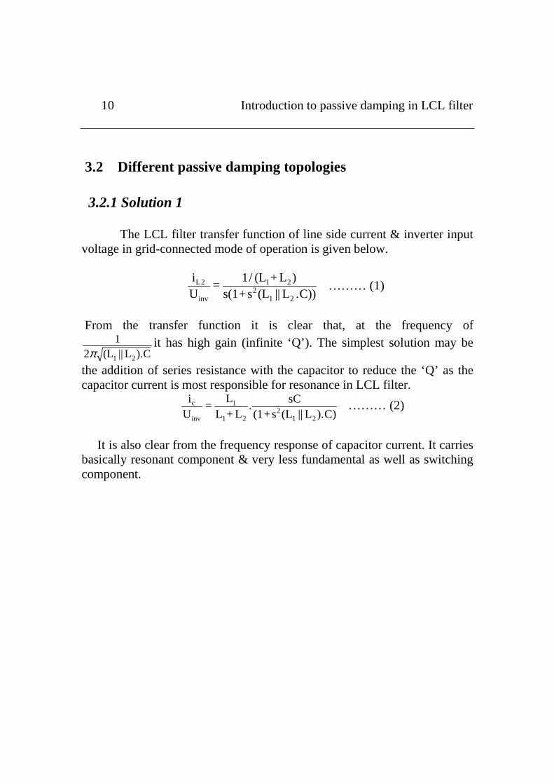
10 Introduction to passive damping in LCL filter 3.2 Different passive damping topologies 3.2.1 Solution 1
The LCL filter transfer function of line side current & inverter input voltage in grid-connected mode of operation is given below.
L2 1 22
1 2inv
i 1/ (L + L )=
U s(1+s (L || L .C)) ……… (1)
From the transfer function it is clear that, at the frequency of
1 2
12 (L || L ).Cπ
it has high gain (infinite ‘Q’). The simplest solution may be
the addition of series resistance with the capacitor to reduce the ‘Q’ as the capacitor current is most responsible for resonance in LCL filter.
c 12
1 2 1 2inv
Li sC= .
U L + L (1+s (L || L ).C) ……… (2)
It is also clear from the frequency response of capacitor current. It carries basically resonant component & very less fundamental as well as switching component.

Different passive damping topologies 11
Fig 3.1 frequency response of the capacitor current in LCL filter
1L
invU
2L
gUdR
C
ciL2i
L1i
Fig 3.2 series damping in LCL filter Fig 3.2 shows the first & the simplest kind of passive damping topology. The bode-plot is given for the capacitor current vs. inverter voltage & line side current Vs inverter output voltage. It is clear from those that larger series resistance can give better damping or lower ‘Q’ as clear from the transfer function after damping.
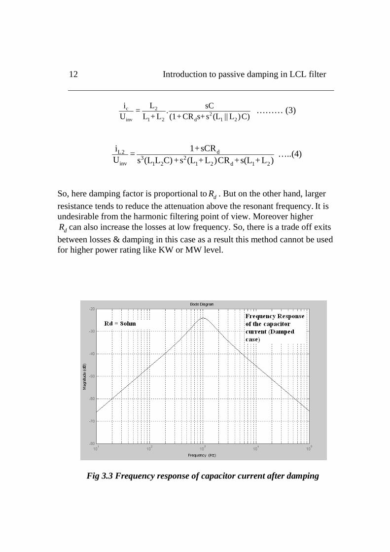
12 Introduction to passive damping in LCL filter
c 22
1 2 1 2inv d
Li sC= .
U L + L (1+ CR s+s (L || L )C) ……… (3)
dL23 2
inv 1 2 1 2 1 2d
1+sCRi=
U s (L L C) +s (L + L )CR +s(L + L ) …..(4)
So, here damping factor is proportional todR . But on the other hand, larger
resistance tends to reduce the attenuation above the resonant frequency. It is undesirable from the harmonic filtering point of view. Moreover higher
dR can also increase the losses at low frequency. So, there is a trade off exits
between losses & damping in this case as a result this method cannot be used for higher power rating like KW or MW level.
Fig 3.3 Frequency response of capacitor current after damping
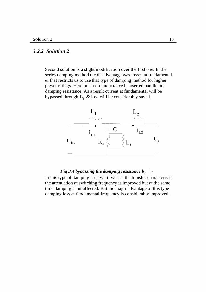
Solution 2 13 3.2.2 Solution 2
Second solution is a slight modification over the first one. In the series damping method the disadvantage was losses at fundamental & that restricts us to use that type of damping method for higher power ratings. Here one more inductance is inserted parallel to damping resistance. As a result current at fundamental will be bypassed through fL & loss will be considerably saved.
1L
invU
2L
gUdR
CL2i
L1i
fL
Fig 3.4 bypassing the damping resistance by fL In this type of damping process, if we see the transfer characteristic the attenuation at switching frequency is improved but at the same time damping is bit affected. But the major advantage of this type damping loss at fundamental frequency is considerably improved.

14 Introduction to passive damping in LCL filter
Fig 3.5 Frequency response with bypassing inductance
3.2.3 Solution 3
1L
invU
2L
gU
dRC
L2iL1i fC
Vc
Fig 3.6 R-C parallel damping for the LCL filter

Solution 3 15 In this type of damping is much more preferred compared to simple series damping as here damping is not only depends on resistance but also on the ‘a’ (fC / C) ratio .It is shown by following frequency plots: -
Fig 3.7 damping by changing fC / C ratio
16 Introduction to passive damping in LCL filter
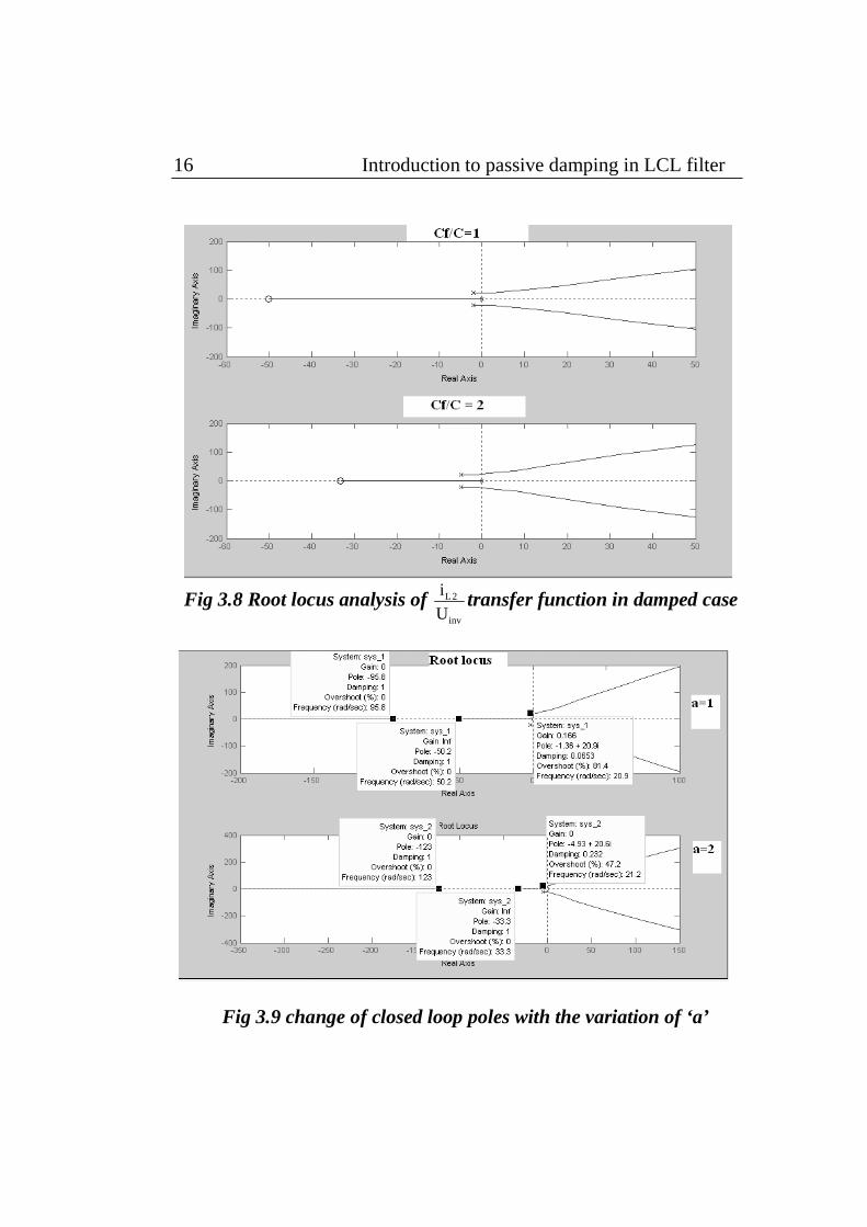
Fig 3.8 Root locus analysis of L2
inv
i
Utransfer function in damped case
Fig 3.9 change of closed loop poles with the variation of ‘a’

Solution 3 17
Fig 3.10 Comparison of transient response with different ‘a’
Fig 3.11 Variation of ‘Q’ with the ‘a’

18 Introduction to passive damping in LCL filter
Now if we see the transfer function,
f dL24 3 2
inv 1 2 f d 1 2 f f f 1 2 1 2
1+ sC Ri
U s L L CC R + s L L (C+ C ) + s C R (L + L ) + s(L + L )=
………………………………………………………… (5) The loss, attenuation & damping (‘Q’ factor) with variation of
fC / C(a) are analyzed below: -
Fig 3.12 overall comparison of Loss, attenuation, damping with
fC / C ratio
Design of ‘a’ 19
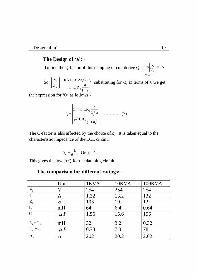
The Design of ‘a’: -
To find the Q-factor of this damping circuit derive Q = c
inv
Vlim = 0.5
U
0ω →
So, c r d d
invr d d
V 0.5+ j0.5w C R=
aU jw C R1+ a
substituting for dC in terms of C we get
the expression for ‘Q’ as follows:-
r d
2
r d 2
a1+ jw CR
1+ aQ =a
jw CR(1+ a)
……….. (7)
The Q-factor is also affected by the choice ofdR . It is taken equal to the characteristic impedance of the LCL circuit.
d
LR =
C Or a = 1.
This gives the lowest Q for the damping circuit. The comparison for different ratings: - Unit 1KVA 10KVA 100KVA
bV V 254 254 254 bI A 1.32 13.2 132 bZ Ω 193 19 1.9
L mH 64 6.4 0.64 C Fµ 1.56 15.6 156
1 2L = L mH 32 3.2 0.32 dC = C Fµ 0.78 7.8 78
dR Ω 202 20.2 2.02

19 Introduction to passive damping in LCL filter
3.3 Conclusion In this chapter several passive damping filters [12] as part of the overall output filter have been discussed. Passive damping is the simplest way of damping resonance excited by this type of filter. But there is trade off between losses and damping in passive damping topologies. Passive damping can be used where the efficiency is not so much of importance or where damping required (Q factor) is not so high. The results of passive damping are given in chapter 7.
Chapter 4
Introduction to Active Damping 4.1 Introduction In case of passive damping, damping provided by physical element like resistors. But this process is associated with losses and in the high power application with process cannot be afforded. To reduce losses and improve the performance inductors, capacitors are provided along with resistors.
In case of active damping, damping is being provided by means of control algorithm, this process is not a lossy process so this process is much more attractive. But there is a limitation of active damping, such as this control technique depends on the switching of power converter, so this is effective only when power converter is switching. On the other hand switching frequency of the power converter is limited hence the control BW of the active damping is also limited. There are broadly two methods of active damping can be thought one is based on traditional PI-controller and the other is based on generalized state-space approach. In this chapter we will focus on a method of active damping based on State-space (arbitrary pole placement)
4.2 Active damping based on traditional approach The traditional approach is based on different current control strategy such as conventional PI-controller based [3] (in rotating frame) combined with lead compensator or a resonant controller as a main compensator in α β− domain. In these approaches BW of the system or settling time cannot be arbitrarily fixed as these based upon main current controller BW. In other words placement of the closed loop poles is determined by the current controller design.
21 Introduction to Active Damping
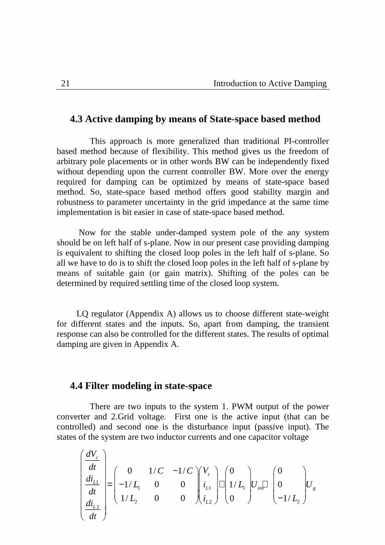
4.3 Active damping by means of State-space based method This approach is more generalized than traditional PI-controller based method because of flexibility. This method gives us the freedom of arbitrary pole placements or in other words BW can be independently fixed without depending upon the current controller BW. More over the energy required for damping can be optimized by means of state-space based method. So, state-space based method offers good stability margin and robustness to parameter uncertainty in the grid impedance at the same time implementation is bit easier in case of state-space based method. Now for the stable under-damped system pole of the any system should be on left half of s-plane. Now in our present case providing damping is equivalent to shifting the closed loop poles in the left half of s-plane. So all we have to do is to shift the closed loop poles in the left half of s-plane by means of suitable gain (or gain matrix). Shifting of the poles can be determined by required settling time of the closed loop system. LQ regulator (Appendix A) allows us to choose different state-weight for different states and the inputs. So, apart from damping, the transient response can also be controlled for the different states. The results of optimal damping are given in Appendix A. 4.4 Filter modeling in state-space There are two inputs to the system 1. PWM output of the power converter and 2.Grid voltage. First one is the active input (that can be controlled) and second one is the disturbance input (passive input). The states of the system are two inductor currents and one capacitor voltage
11 1 1
2 222
0 1/ 1/ 0 0
1/ 0 0 1/ 0
1/ 0 0 1/0
c
c
LL inv g
LL
dV
dt VC Cdi
L i L U Udt
L Lidi
dt
− = − + +
−

4.5 Pole-placement of the system 22 So in more compact form, ………. (1) ……….. (2) Where the matrices are following,
So, the eigen values of system are
Now position of the poles are on imaginary axis hence the system is oscillatory and highly sensitive to outside disturbances. 4.5 Pole-placement of the system Typical scheme (in brief) for active damping control can be visualized by the following figure.
1
2
0 1/ 1/
1/ 0 0
1/ 0 0LCL
C C
A L
L
− = −
1 1
0
1/
0
B L
=
2
2
0
0
1/
B
L
= −
1 0 0
0 1 0LCLC
=
1 2
10,
( || ).j
L L Cλ +
−=
.
1 2LCL LCL inv
LCL LCL
x A x B u B ug
y C x
= + +=
23 Introduction to Active Damping
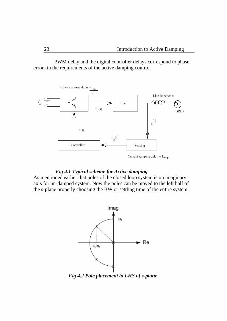
PWM delay and the digital controller delays correspond to phase errors in the requirements of the active damping control.
Fig 4.1 Typical scheme for Active damping As mentioned earlier that poles of the closed loop system is on imaginary axis for un-damped system. Now the poles can be moved to the left half of the s-plane properly choosing the BW or settling time of the entire system.
Fig 4.2 Pole placement to LHS of s-plane

Per unitization 24 Let the imaginary axis pole is to be shifted to Where the is the damping factor of the system. Here only task to choose this damping factor for designing this system. is taken as 0.6 (sufficient to provide the damping) For assigning above pole in the system we use control law
inv LCLU = -KX Or in other words inv 1 c 2 L1 3 L2U = -K V - K i - K i ….. (3) The task is to find the gain matrix for the system. For that system is per unitized. Per unitization:- For 10KVA inverter and 440V grid voltage we can per unitized the system.
L1=L2 = 3mH and C = 16 Fµ can be per unitized as L1 = L2 = 0.05p.u
C = 0.09p.u …….. (4) Now the required pole placement @ Hence the required gain matrix is K= [-0.0005 1.5 -1.5].
21r rjξω ω ξ+− −
ξξ
12.25 16.32j+−−
c
c
L1L1 inv g
L2L2
dV
dt V0 20 -20 0 0di
= -10.3 0 0 i + 10.3 U + 0 Udt
10.3 0 0 0 -10.3idi
dt
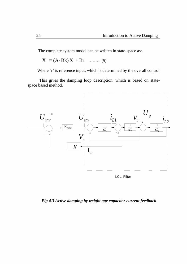
25 Introduction to Active Damping The complete system model can be written in state-space as:- …….. (5) Where ‘r’ is reference input, which is determined by the overall control This gives the damping loop description, which is based on state-space based method.
PWMK1
1
sL
1
sC 2
1
sL
*invU invU
cV
1Li cV2Li
gU
Kci
LCL Filter Fig 4.3 Active damping by weight age capacitor current feedback
.
X = (A- Bk)X + Br

4.6 Physical realization of Active Damping (concepts of Virtual
resistance) 26
4.7 Physical realization of Active Damping (concepts of Virtual resistance)
The concepts of active damping can be realized from the equation (5). After splitting the state-space form we get, So, if we try to give the circuit form of the above equation then it approximately looks like:-
invUgU
1LvR
1(1 ) cK V+ 2L
C
pR
1Li 2Li
cV
Fig 4.4 Approximate Circuit representation for Active damping
cL1 L2
L11 1 c 2 L1 3 L2 inv
L22 c g
dVC = i - i . - - - 6 .
dtdi
L = -(1+ )V - i - i + U - - - - - 7 .dtdi
L = V - U - - - - - - 8 .dt
K K K
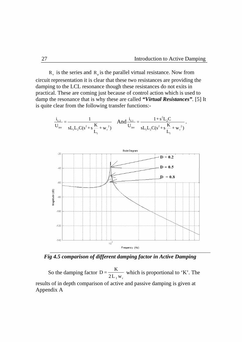
27 Introduction to Active Damping vR is the series and pR is the parallel virtual resistance. Now from
circuit representation it is clear that these two resistances are providing the damping to the LCL resonance though these resistances do not exits in practical. These are coming just because of control action which is used to damp the resonance that is why these are called “Virtual Resistances”. [5] It is quite clear from the following transfer functions:-
L2
2 2inv1 2 r
1
i 1=
KU sL L C(s +s + w )L
And2
L1 2
2 2inv1 2 r
1
i 1+ s L C=
KU sL L C(s +s + w )L
.
Fig 4.5 comparison of different damping factor in Active Damping
So the damping factor 1 r
KD =
2L w which is proportional to ‘K’. The
results of in depth comparison of active and passive damping is given at Appendix A

4.8 Active damping loop realization 28
4.8 Active damping loop realization
The following figure shows the general practical approach of active damping loop. It consists of three feedbacks like two inductor currents and one capacitor voltage though it is shown that there is no need of feeding backs the capacitor voltage for arbitrary pole placements. But in the case of optimal damping (Appendix A) all the three feedback signals are needed.
INVERTER
PWM Pulse generation
Gate pulses for IGBTZC
Current sense voltage sense
L1 L2 Vc
Active
C
Processing
1Li2Li
gUCurrent sense
Fig 4.6 State-space based active damping loop (general case)

29 Introduction to Active Damping
Fig 4.7 Comparison of virtual resistance based damping and actual
resistance based damping of L2
inv
i
Utransfer function
4.9 Conclusion
Active damping by means of state-space based method is much more robust compared to other ones. The implementation of the state-space based method is much simpler than complex control topology. The active damping implemented in MATLAB/SIMULINK and also in practically. The results are given in chapter 7 and 8.

Chapter 5 Grid synchronization & Introduction to Phase Locked Loop 5.1 Introduction A phase locked loop is used in applications where tracking of phase and frequency of the incoming signal is necessary. For grid connected applications of power converters such as distributed generation and power quality improvement, a PLL is used to generate unit sine and cosine signals synchronized to system frequency from utility voltage. Closed loop control of power converters in synchronous reference frame method needs these unit sine and cosine signals to compute feedback and modulating signals. Here SRF based (Synchronous frame based) algorithm is described. It is robust algorithm that also works under abnormal grid condition. 5.2 PLL algorithm
Fig 5.1 Basic PLL structure
31 Grid synchronization & Introduction to Phase Locked Loop
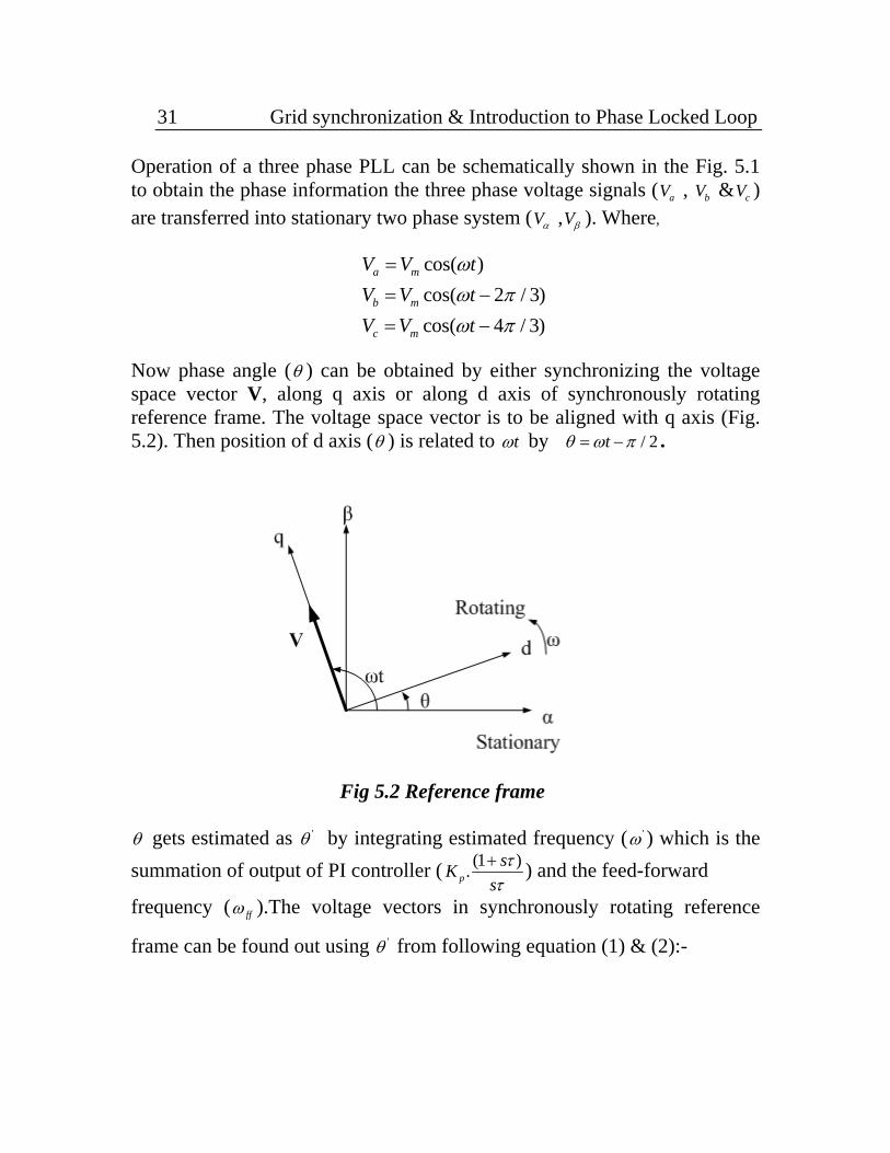
Operation of a three phase PLL can be schematically shown in the Fig. 5.1 to obtain the phase information the three phase voltage signals ( aV , bV & cV ) are transferred into stationary two phase system (Vα ,Vβ ). Where,
cos( )cos( 2 / 3)cos( 4 / 3)
a m
b m
c m
V V tV V tV V t
ωω πω π
== −
= −
Now phase angle (θ ) can be obtained by either synchronizing the voltage space vector V, along q axis or along d axis of synchronously rotating reference frame. The voltage space vector is to be aligned with q axis (Fig. 5.2). Then position of d axis (θ ) is related to tω by / 2tθ ω π= − .
Fig 5.2 Reference frame θ gets estimated as 'θ by integrating estimated frequency ( 'ω ) which is the summation of output of PI controller ( (1 ).p
sKsτ
τ+ ) and the feed-forward
frequency ( ffω ).The voltage vectors in synchronously rotating reference
frame can be found out using 'θ from following equation (1) & (2):-
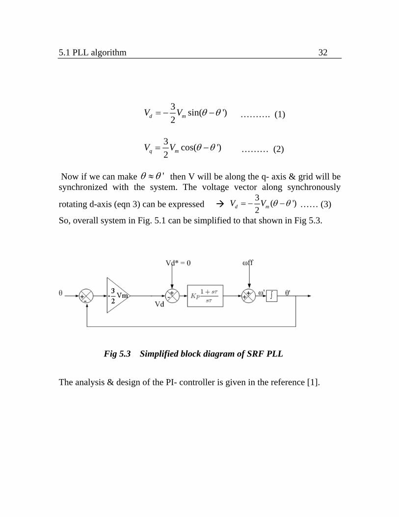
5.1 PLL algorithm 32
3 sin( ')2d mV V θ θ= − − ………. (1)
3 cos( ')2q mV V θ θ= − ……… (2)
Now if we can make 'θ θ≈ then V will be along the q- axis & grid will be synchronized with the system. The voltage vector along synchronously
rotating d-axis (eqn 3) can be expressed 3 ( ')2d mV V θ θ= − − …… (3)
So, overall system in Fig. 5.1 can be simplified to that shown in Fig 5.3.
Fig 5.3 Simplified block diagram of SRF PLL The analysis & design of the PI- controller is given in the reference [1].
33 Grid synchronization & Introduction to Phase Locked Loop
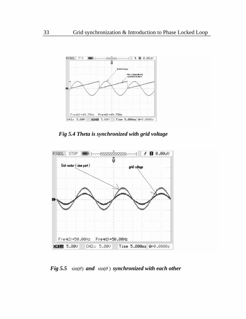
Fig 5.4 Theta is synchronized with grid voltage
Fig 5.5 sin( )θ and 'sin( )θ synchronized with each other

5.3 Conclusion 34 5.3 Conclusion A three-phase PLL system is presented here for utility interface applications. Operation is suitable especially under distorted utility conditions such as line harmonics and frequency disturbances but in the present case balanced grid is assumed. The PLL is completely implemented in inside FPGA based controller as well as in practically without the use of any hardware filters. All analytical results were experimentally verified.

35 5.3 Conclusion
Chapter 6
Control Scheme for Standalone and Grid Interactive Mode with LCL Filter 6.1 Introduction Here in this chapter dq-based control strategy [1] is adopted. The control scheme for LCL filter based system is quite different as well as complicated from those of simple L filter based grid-connected system. The number of sensors is also more in case of LCL filter. Control scheme that is described, can be applicable to both in standalone and grid parallel mode. Initially current controllers, voltage controller and then at last State-space based damping loop is described. 6.2 Model for control design For control design, the grid is modeled as an ideal sinusoidal three phase voltage source without line impedances, although, in reality there are line impedances and distortions like line harmonics and unbalances. The space notation is used. Three phase values are transformed into the dq-reference frame that rotates synchronously with the line voltage space vector. From control point of view it is advantageous to control dc values since PI controller can achieve reference tracking without steady state errors. Modeling of the LCL filter in the dq-reference frame without frequency dependences of the inductances is performed here.

37 Control Scheme for Standalone and Grid Interactive Mode with
LCL Filter
Fig 6.1 Active rectifier with LCL filter Simplified model for Grid connected mode
1L
invU
2L
gUCci
L2iL1i
Vc
Fig 6.2 Grid connection with LCL filter
GridGrid
GridC
L1 L2
L2L1
C C
R
Y
B
Neutral
Active Rectifier
O
1Li 2LicV
L1LOAD
dcidcV
Loadi
N
L2
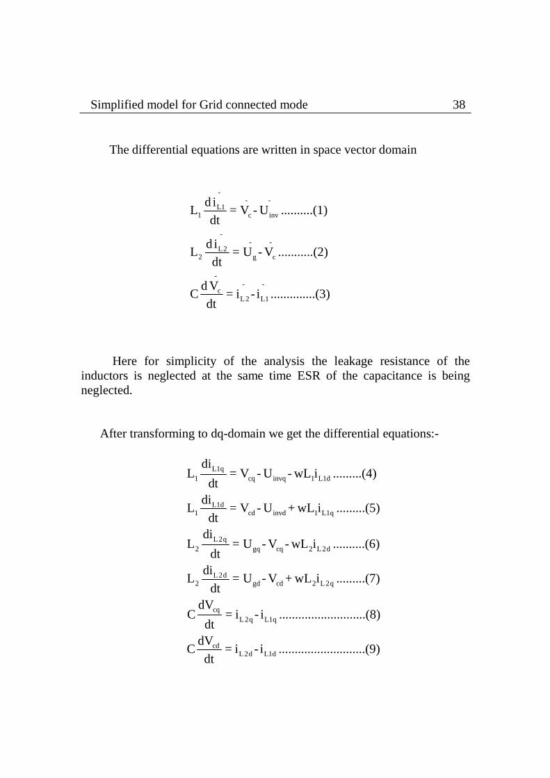
Simplified model for Grid connected mode 38 The differential equations are written in space vector domain
-- -
L11 c inv
-- -
L22 g c
-- -
cL 2 L1
d iL = V - U ..........(1)
dt
d iL = U - V ...........(2)
dt
d VC = i - i ..............(3)
dt
Here for simplicity of the analysis the leakage resistance of the inductors is neglected at the same time ESR of the capacitance is being neglected. After transforming to dq-domain we get the differential equations:-
L1q1 cq invq 1 L1d
L1d1 cd invd 1 L1q
L 2q2 gq cq 2 L 2d
L 2d2 gd cd 2 L 2q
cqL 2q L1q
diL = V - U - wL i .........(4)
dtdi
L = V - U + wL i .........(5)dt
diL = U - V - wL i ..........(6)
dtdi
L = U - V + wL i .........(7)dt
dVC = i - i ...........................(8)
dt
cdL 2d L1d
dVC = i - i ...........................(9)
dt
39 Control Scheme for Standalone and Grid Interactive Mode with LCL Filter
Now if we include the dynamics of the DC-bus voltage of the power converter we get,
L2q gqdc
dc dc load loaddc
i UdV 3C = i - i = - i .......(10)
dt 2 V
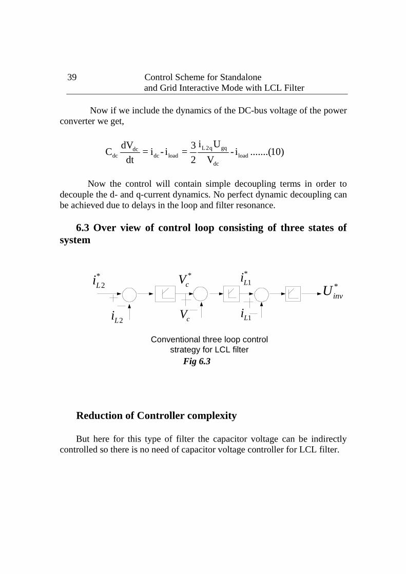
Now the control will contain simple decoupling terms in order to decouple the d- and q-current dynamics. No perfect dynamic decoupling can be achieved due to delays in the loop and filter resonance. 6.3 Over view of control loop consisting of three states of system
*2Li
2Li
*cV
cV 1Li
*1Li *
invU
Conventional three loop control strategy for LCL filter
Fig 6.3 Reduction of Controller complexity But here for this type of filter the capacitor voltage can be indirectly controlled so there is no need of capacitor voltage controller for LCL filter.

Two loop control strategy for LCL filter 40
The L2 L1 ci - i = i and the c c
1V = i dt
C∫ , hence if we can control
L1i and L 2i separately then that itself control the ci followed
by the cV . Two Loop current control Strategy for LCL filter Now the control loop may be reduced to following fashion:-
*2Li
2Li 1Li
*1Li
*invU
Two loop control strategy for LCL filter Fig 6.4 So here the output of the line side current controller is becoming the reference of converter side current. Now here line side current and converter side current are almost equal in magnitude and phase in fundamental as capacitor size is limited in LCL filter because of reactive power burden. Hence further more simplification is possible. The converter side current controller can also be omitted and only line side current controller is fair enough to control the current. The output of line side current controller will become inverter input reference.

41 Control Scheme for Standalone and Grid Interactive Mode with LCL Filter
*2Li
2Li
*invU
Single loop control strategy for LCL filter
Fig 6.5 Limitation of Single loop control strategy for LCL filter Single grid current loop controller is not sufficient for stability of the overall system. The resonance of the filter can make the system unstable as here we are only concentrating on the fundamental current where LCL filter has significant amount of resonance frequency super imposed over the fundamental. So we need to consider the resonance carefully. Higher-level control [10] loops are required to provide fast dynamic compensation for the system disturbances and improve stability. 6.4 Current control strategy Conventional PI controller [7] in innermost loops is not reasonable from point of view of speed and complexity. Basically in order to control the resonance in the filter inner most current loop should be very fast (ideally instantaneous). So, for this type of filters inner most current loop ( L1i ) can be designed by a proportional controller. This controller or this inner loop makes the system dynamic response very good by limiting the unwanted
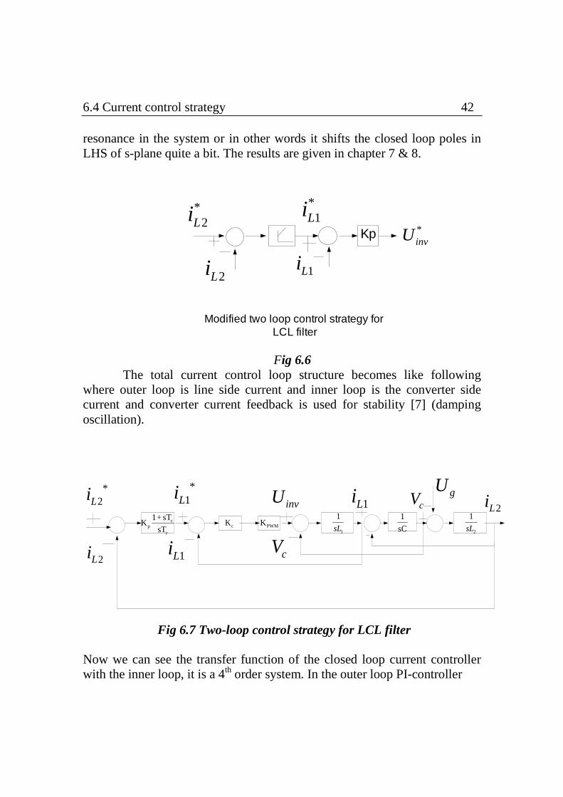
6.4 Current control strategy 42 resonance in the system or in other words it shifts the closed loop poles in LHS of s-plane quite a bit. The results are given in chapter 7 & 8.
Kp
*2Li
2Li 1Li
*1Li
*invU
Modified two loop control strategy for LCL filter
Fig 6.6 The total current control loop structure becomes like following where outer loop is line side current and inner loop is the converter side current and converter current feedback is used for stability [7] (damping oscillation).
cp
c
1+ sTK
sT cK PWMK1
1
sL
1
sC 2
1
sL
*2Li
2Li
*1Li
1Li
invU
cV
1Li cV2Li
gU
Fig 6.7 Two-loop control strategy for LCL filter Now we can see the transfer function of the closed loop current controller with the inner loop, it is a 4th order system. In the outer loop PI-controller

43 Control Scheme for Standalone and Grid Interactive Mode with LCL Filter
used as usual and proportional controller is used in inner loop. The closed loop transfer function is given below, is used to analyze the stability.
*p c PWM p c PWM cL2
4 3 2L2 1 2 c PWM 2 1 2 p c PWM c PWM p c PWM c
(K K K )s+ K K K / Ti=
i (L L C)s + (K K L C)s + (L + L )s + (K K K + K K )s+ K K K / T
......... (11) 6.5 Analysis of controller performance
A. Analysis of the outer loop
The outer loop is a PI-controller, where the value of pK should be quite high value to track the reference but at the same time
pK should not be as large as wish, which can be seen from the following analysis. As it grows bigger, the poles will shift towards the right side of s-plane.
Fig 6.8 Root locus of *
L2
L2
i
i with pK = 0.5
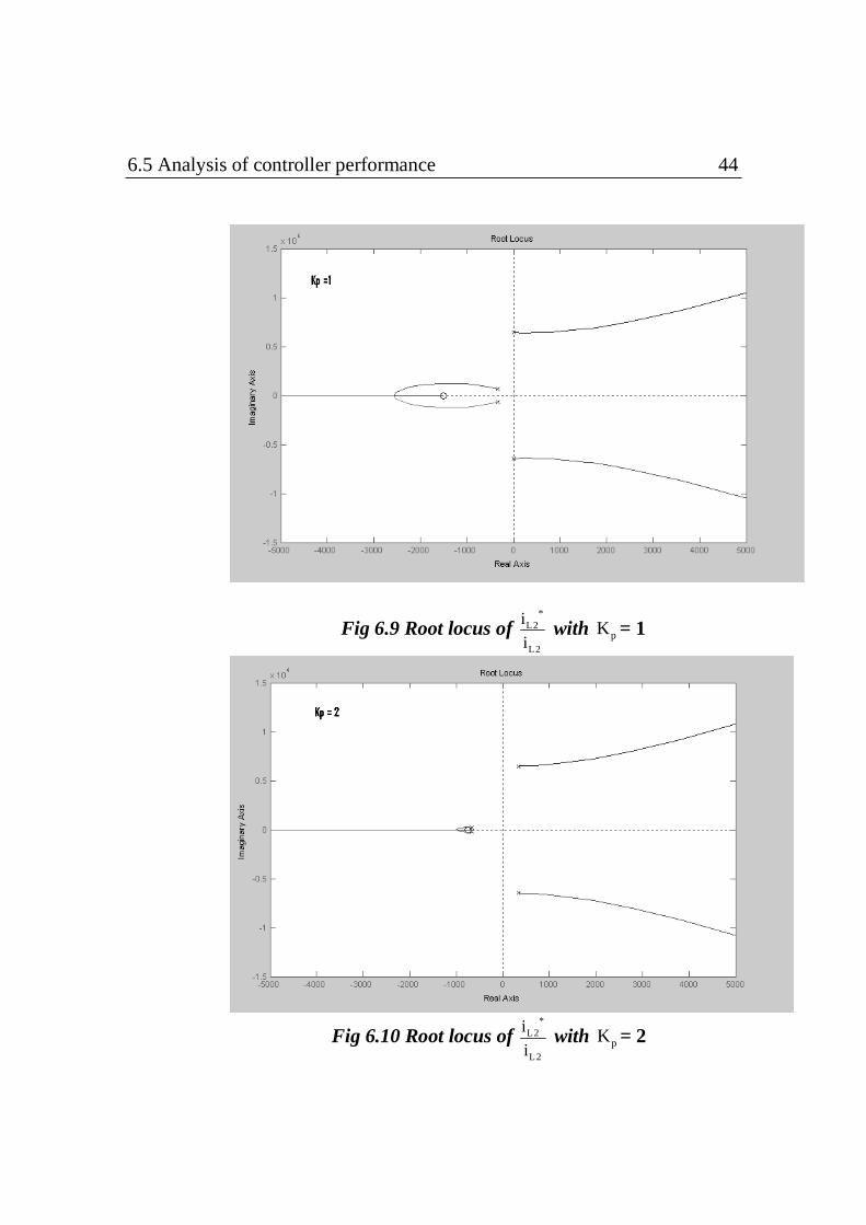
6.5 Analysis of controller performance 44
Fig 6.9 Root locus of *
L2
L2
i
i with pK = 1
Fig 6.10 Root locus of *
L2
L2
i
i with pK = 2

45 Control Scheme for Standalone and Grid Interactive Mode with LCL Filter
B. Analysis of the inner loop
The inner loop basically improves the stability of the system and increases the robustness. In other words more important role of the inner loop is to damp the resonance peak but at the same time very high of cK can make system unstable also. So, the value of
cK has to be limited and we cannot depend the value of cK to damp the oscillation.
Fig 6.11 Bode plot of *
L2
L2
i
i with different value of Kc

6.6 Inclusion of inner most state-space based damping loop 46
6.6 Inclusion of innermost state-space based damping loop
As mentioned earlier that in the converter current loops the value of cK is limited from the point of view of stability. So, when high damped system is desired this method of damping not so much preferable. The state-space based method offer more flexibility of choosing the controller parameter and at the same time robustness. The total current control loop with the damping loop is shown below
cp
c
1+ sTK
sTPWMK
1
1
sL
1
sC 2
1
sL
*2Li
2Li
*invU invU
cV
1Li cV2Li
gU
K
Control partPower
converterLCL filter
Fig 6.12 Current control with State-space based damping loop
47 Control Scheme for Standalone and Grid Interactive Mode with LCL Filter
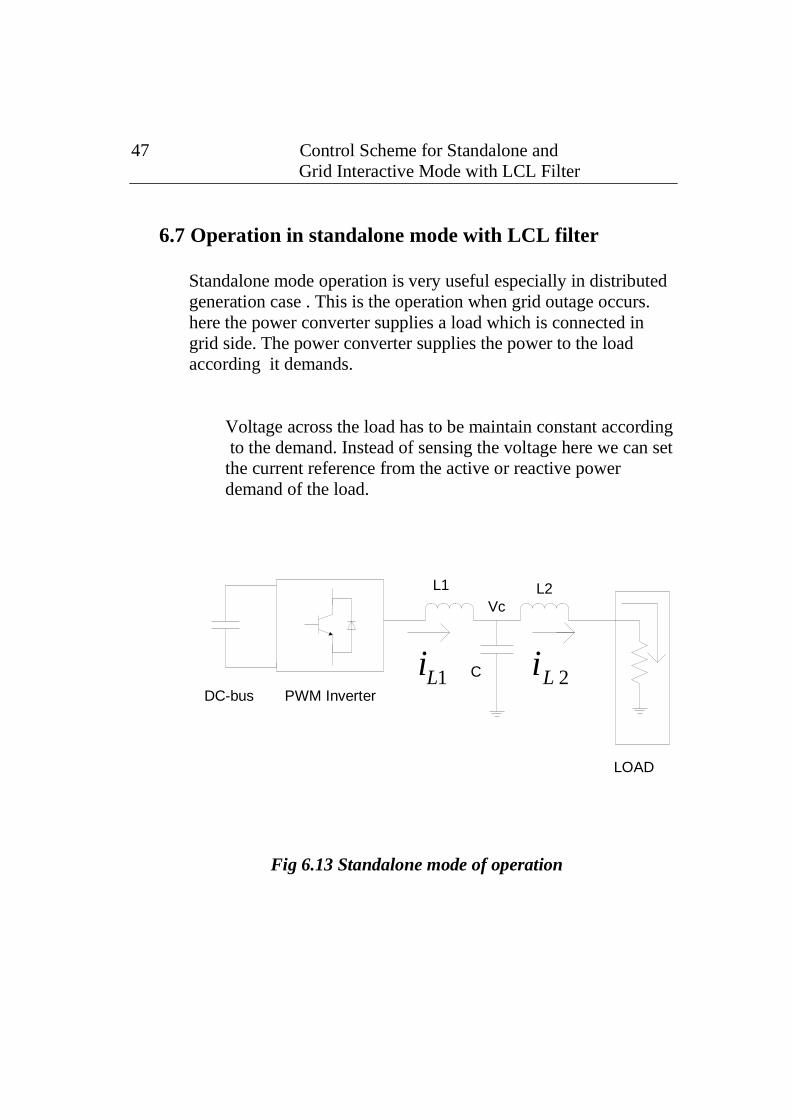
6.7 Operation in standalone mode with LCL filter Standalone mode operation is very useful especially in distributed generation case . This is the operation when grid outage occurs. here the power converter supplies a load which is connected in grid side. The power converter supplies the power to the load according it demands. Voltage across the load has to be maintain constant according to the demand. Instead of sensing the voltage here we can set the current reference from the active or reactive power demand of the load. Fig 6.13 Standalone mode of operation
PWM InverterDC-bus
L1 L2
C
LOAD
Vc
1Li 2Li

6.7 Control in standalone mode with LCL filter 48 6.7 Control in standalone mode with LCL filter Here in standalone mode voltage loop is neglected as current reference is being generated from the active power reference. The complete vector control of the system is shown below which include active damping loop also in that. The results are given in chapter 7,8 and also in Appendix C
abc-dq
PLLAlgorithm
Decoupling & dq-abc
2L abci
1L abci
gabcU
1 cp
c
sTK
sT
+
1 cp
c
sTK
sT
+
*2L di
2L di
2L qi
*2L qi
sensed
sensed
sensed
θ
K
cabci
*invU
PWMKPWMK
invabcU
Fig 6.14 Vector control of standalone mode Here though the grid is not connected but the unit vector is generated from the grid only by SRF based PLL algorithm. Single grid current control loop with the state-space damping loop is included to damp the un-wanted resonance of LCL filter. 6.8 Control in grid parallel mode with LCL filter In grid connected mode load is connected across the DC-bus, which is to be supplied from the grid with good power quality (FEC mode)[16]. So,

49 Control Scheme for Standalone and Grid Interactive Mode with LCL Filter
naturally the load voltage has to be maintaining constant. Here DC-link voltage controller is must for this kind of operation.
PLLAlgorithm
Decoupling & dq-abc
*dcV
gabcU
1 cp
c
sTK
sT
+
1 cp
c
sTK
sT
+
*2L di
2L di
2L qi
*2L qi
θ
K
cabci
*invabcU
PWMKPWMK
invabcU1 dc
dcdc
sTK
sT
+
dcV
sensed
sensed
Reactive Power reference
Active Power reference
Fig 6.15 Vector control in grid parallel mode 6.9 Sensor less operation In the control of LCL filter based system (grid connected or standalone mode) consists of several loops cascaded. Naturally while doing the implementation in practice it needs quite a few sensors. These sensors, specially the LEM current sensors are costly hence it is better to use minimal number of sensors.
6.10 Conclusion 50 So, in the LCL filter based system the idea of minimizing sensors really makes sense. The way out is to estimate the corresponding quantities like voltages or currents. There are two ways to eliminate sensors, one way to run a parallel process in the controller and then calculate quantities and use for control, the second way to design the reduced order observer to estimate the states. 6.10 Conclusion The control strategies that is described in this chapter equally applicable for standalone and grid parallel mode with very little difference. The above control strategy is simulated and experimentally verified and results are given in chapter 7 and 8.

51 6.10 Conclusion

Chapter 7
Simulation Results 7.1 Introduction The entire system is simulated in standalone and grid connected mode. The system parameters are specified in the following table. The simulation is carried out in MATLAB/SIMULINK software. At first the standalone mode results are presented followed by grid connected mode results. 7.2 System parameters Symbols Values used
gU 100-200V (L-n)
dcV 400-550V
1L 3mH
2L 3mH C 16 Fµ
swf 5-10KHz f 50Hz
dcC 3300 Fµ Load (grid connected mode) 100-200ohm Load (in standalone mode) 10-20ohm

53 Simulation Results
7.3 Standalone mode results These are the results that are simulated in standalone mode (Power circuit in chapter 6). Actually this mode of operation is essential from point of proving the controller performance as in this case we can test the each loop separately (current control loop, damping loop).This flexibility is not available in grid parallel mode where all control has to be worked in cascaded manner. Hence this mode of operation is essential before going to grid interactive mode. - Actually the current control loop & damping loops are decoupled in the sense, their BW is well apart. So for current loop sees the damping loop instantaneous similar reasons applicable for voltage loop & current loop. So, we can test these loops separately & verify. System has simulated in all condition like with damping, without damping, with load & without load & functions of all the three loops are shown separately. In standalone mode the all the results are with 20ohms load in the grid side Figs 7.1 to 7.5 are the results of standalone mode without damping. Figs 7.6 to 7.10 are the results of standalone mode with damping. 7.4 Grid connected mode results In this mode all the three loops like voltage (DC-bus loop), current (grid current loop) & active damping loop are cascaded one after other. DC-bus loop is the outer most loops so naturally much slower compared to other two. Hence while designing the DC-bus loop the other loop are taken as one. Similarly for the current loop, damping loop is taken as one.

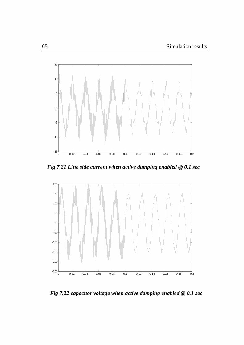
7.4 Grid connected mode results 54 Figs 7.11 to 7.15 are the results of grid connected mode with damping and with no-load Figs 7.16 to 7.20 are the results of grid connected mode with damping and with load Figs 7.21 to Fig 7.23 are the results of Active damping in grid parallel mode
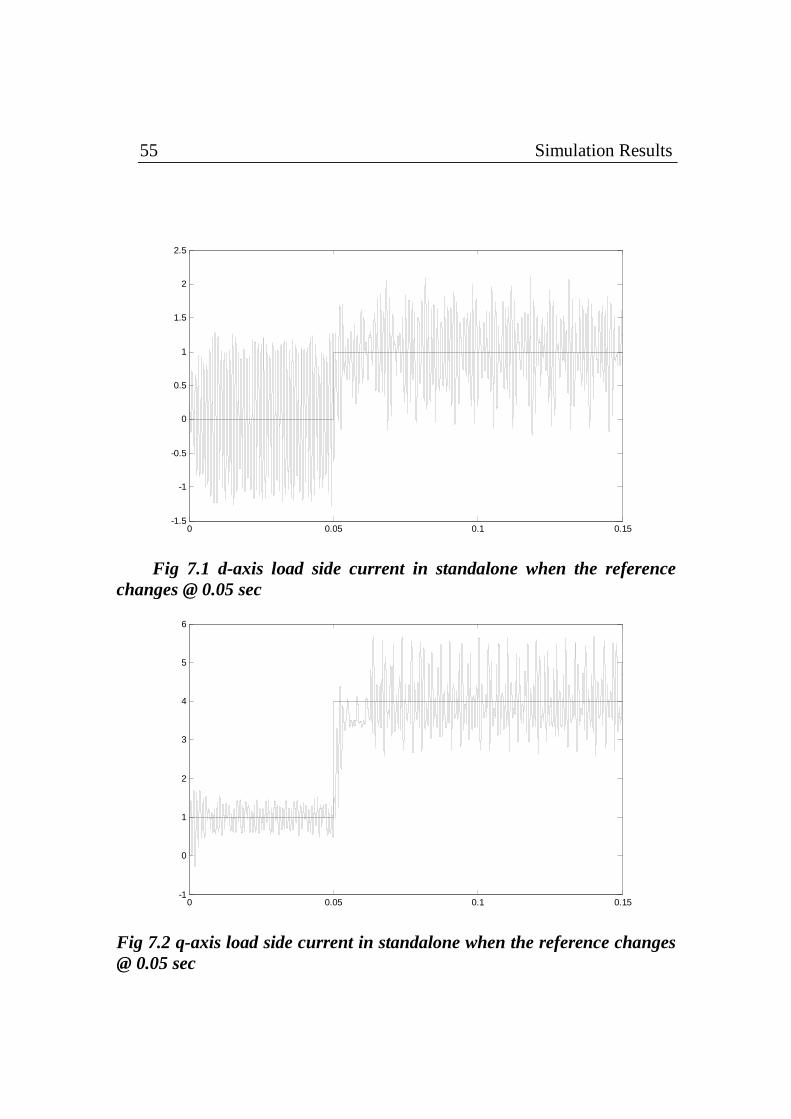
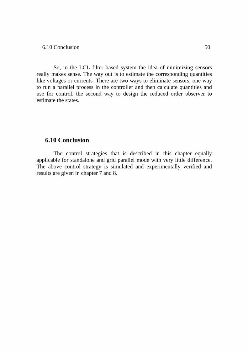
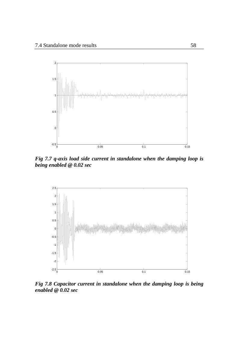
55 Simulation Results
0 0.05 0.1 0.15-1.5
-1
-0.5
0
0.5
1
1.5
2
2.5
Fig 7.1 d-axis load side current in standalone when the reference changes @ 0.05 sec
0 0.05 0.1 0.15-1
0
1
2
3
4
5
6
Fig 7.2 q-axis load side current in standalone when the reference changes @ 0.05 sec

7.3 Standalone mode results 56
0 0.05 0.1 0.15-4
-3
-2
-1
0
1
2
3
4
Fig 7.3 R-phase load side current in standalone when the reference changes @ 0.05 sec
0 0.05 0.1 0.15-4
-3
-2
-1
0
1
2
3
4
Fig 7.4 capacitor current in standalone when the reference changes @ 0.05 sec

57 Simulation results
0 0.05 0.1 0.15-80
-60
-40
-20
0
20
40
60
80
Fig 7.5 Capacitor voltage in standalone when the reference changes @ 0.05 sec
0 0.05 0.1 0.15-1.5
-1
-0.5
0
0.5
1
1.5
Fig 7.6 d-axis load side current in standalone when the damping loop is being enabled @ 0.02 sec
7.4 Standalone mode results 58
0 0.05 0.1 0.15-0.5
0
0.5
1
1.5
2
Fig 7.7 q-axis load side current in standalone when the damping loop is being enabled @ 0.02 sec
0 0.05 0.1 0.15-2.5
-2
-1.5
-1
-0.5
0
0.5
1
1.5
2
2.5
Fig 7.8 Capacitor current in standalone when the damping loop is being enabled @ 0.02 sec
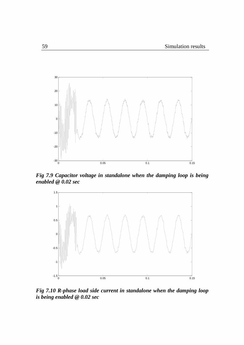
59 Simulation results
0 0.05 0.1 0.15-30
-20
-10
0
10
20
30
Fig 7.9 Capacitor voltage in standalone when the damping loop is being enabled @ 0.02 sec
0 0.05 0.1 0.15-1.5
-1
-0.5
0
0.5
1
1.5
Fig 7.10 R-phase load side current in standalone when the damping loop is being enabled @ 0.02 sec
7.4 Grid connected mode results 60
0 0.05 0.1 0.15-1
0
1
2
3
4
5
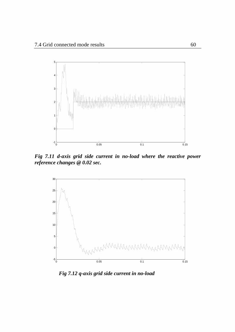
Fig 7.11 d-axis grid side current in no-load where the reactive power reference changes @ 0.02 sec.
0 0.05 0.1 0.15-5
0
5
10
15
20
25
30
Fig 7.12 q-axis grid side current in no-load

61 Simulation results
0 0.05 0.1 0.15-20
-15
-10
-5
0
5
10
15
Fig 7.13 grid side current in no-load
0 0.05 0.1 0.15240
250
260
270
280
290
300
310
Fig 7.14 DC-link voltage profile in no load

7.4 Grid connected mode results 62
0 0.05 0.1 0.15-1000
-800
-600
-400
-200
0
200
400
600
800
1000
Fig 7.15 Fundamental of R-phase inverter voltage& grid voltage of R-phase
0 0.05 0.1 0.15-1
0
1
2
3
4
5
Fig 7.16 d-axis current of grid side with load

63 Simulation results
0 0.05 0.1 0.15-5
0
5
10
15
20
25
30
Fig 7.17 q-axis current of grid side with load enabled @ 0.08sec
0 0.05 0.1 0.15-20
-15
-10
-5
0
5
10
15
Fig 7.18 line side current of R-phase with load enabled @ 0.08sec

7.4 Grid connected mode results 64
0 0.5 1 1.5 2 2.5 3240
260
280
300
320
340
360
380
400
420
Fig 7.19 DC-link voltage profile when the load is being enabled @ 1.5sec
0 0.02 0.04 0.06 0.08 0.1 0.12 0.14 0.16 0.18 0.2-150
-100
-50
0
50
100
150
Fig 7.20 Line side current & line voltage with UPF operation
65 Simulation results
0 0.02 0.04 0.06 0.08 0.1 0.12 0.14 0.16 0.18 0.2-15
-10
-5
0
5
10
15
Fig 7.21 Line side current when active damping enabled @ 0.1 sec
0 0.02 0.04 0.06 0.08 0.1 0.12 0.14 0.16 0.18 0.2-250
-200
-150
-100
-50
0
50
100
150
200
Fig 7.22 capacitor voltage when active damping enabled @ 0.1 sec

7.5 Conclusion 66
0 0.02 0.04 0.06 0.08 0.1 0.12 0.14 0.16 0.18 0.2-10
-8
-6
-4
-2
0
2
4
6
8
Fig 7.23 capacitor current when active damping enabled @ 0.1 sec 7.5 Conclusion Here in this chapter the entire system is simulated in two modes Standalone and Grid connected mode. The test of controller can be only be done in standalone only. Hence the controller test results are given in standalone mode and test of active damping results are given in FEC mode as well as in standalone mode.

67 7.5 Conclusion

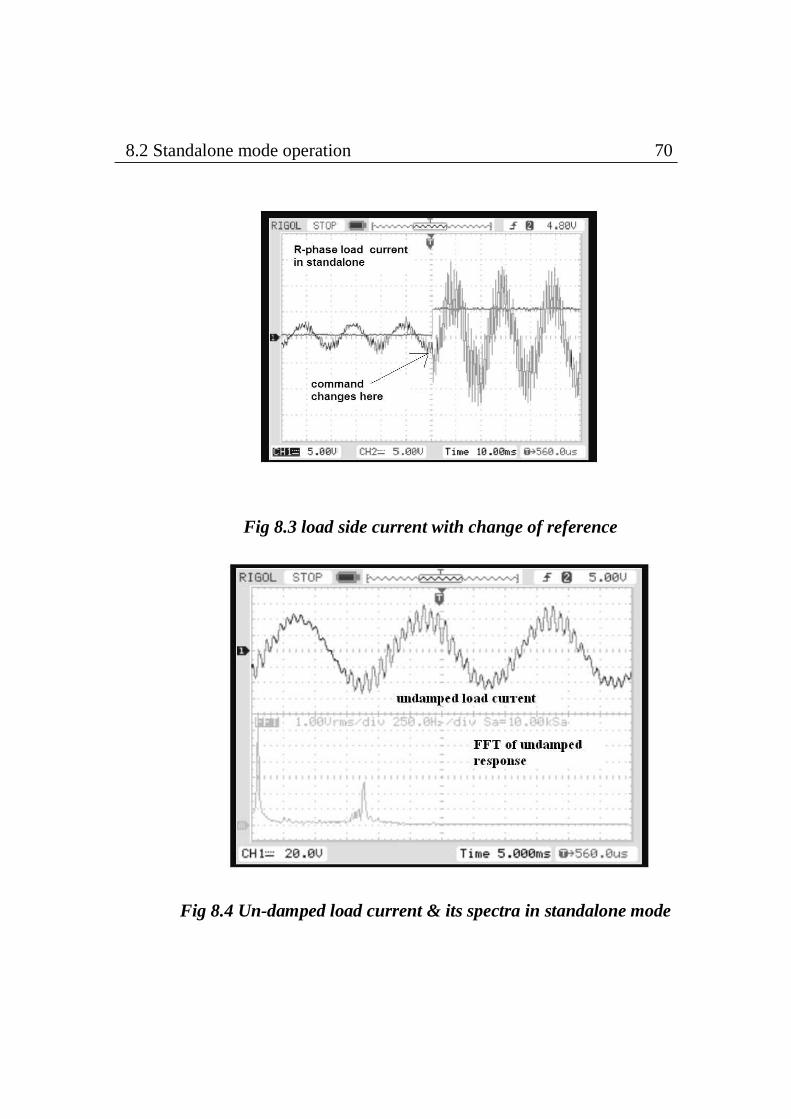
Chapter 8
Experimental Results 8.1 Introduction The system has experimentally verified on 10KVA power converter which is operated in standalone mode & FEC mode with LCL filter in Lab. Parameters are same as in simulation. 8.2 Standalone Mode of operation Figs 8.1 to 8.3 are the results of standalone mode without damping. Figs 8.4 to 8.10 are the results of standalone mode with damping. 8.3 grid parallel mode of operation Figs 8.11 to Fig 8.20 are the results of grid parallel mode including damping loops.

69 Experimental Results
Fig 8.1 q-axis load side current with change of reference
Fig 8.2 q-axis load side current with change of reference
8.2 Standalone mode operation 70
Fig 8.3 load side current with change of reference
Fig 8.4 Un-damped load current & its spectra in standalone mode

71 Experimental Results
Fig 8.5 Damped load current & its spectra in standalone mode
Fig 8.6 Active damping test of load current with lesser state-weight age
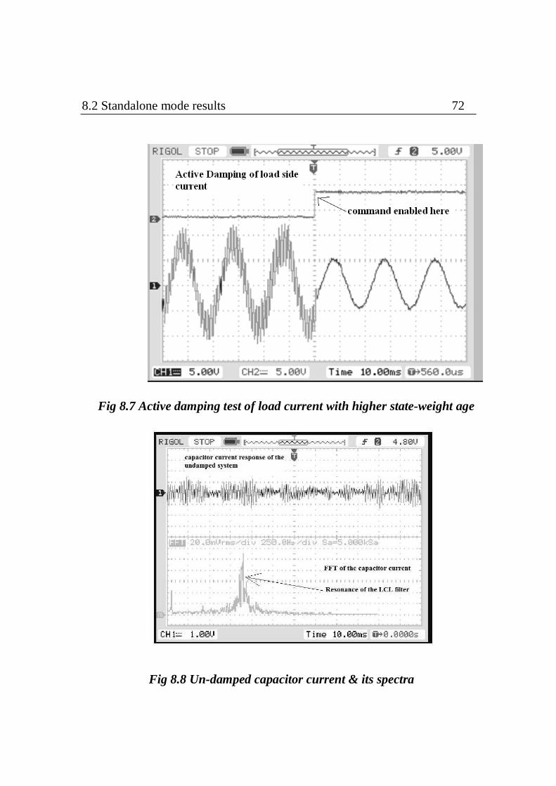
8.2 Standalone mode results 72
Fig 8.7 Active damping test of load current with higher state-weight age
Fig 8.8 Un-damped capacitor current & its spectra

73 Experimental Results
Fig 8.9 Active damping test of capacitor current
Fig 8.10 Active damping test of q-axis capacitor current
8.3 Grid connected mode results 74
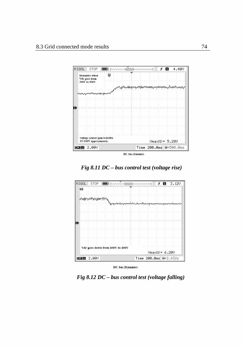
Fig 8.11 DC – bus control test (voltage rise)
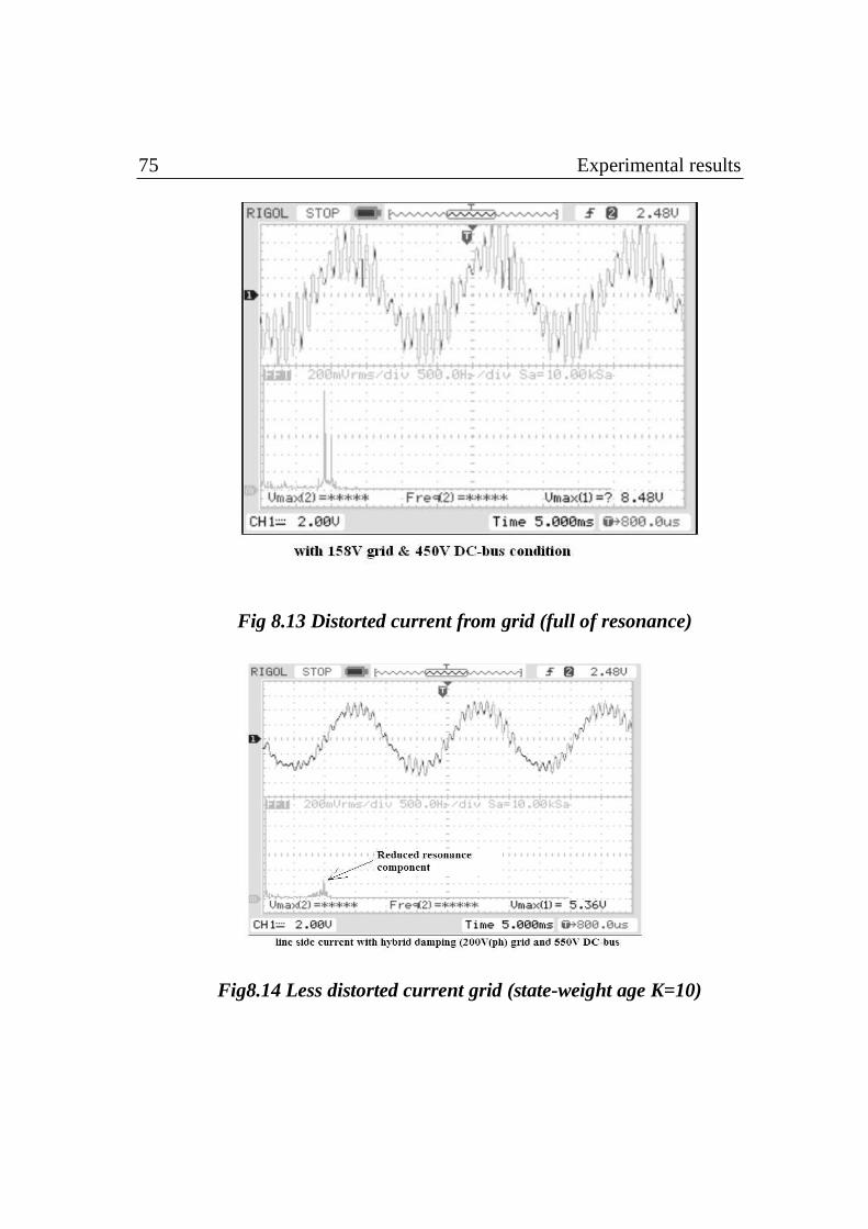
Fig 8.12 DC – bus control test (voltage falling)
75 Experimental results
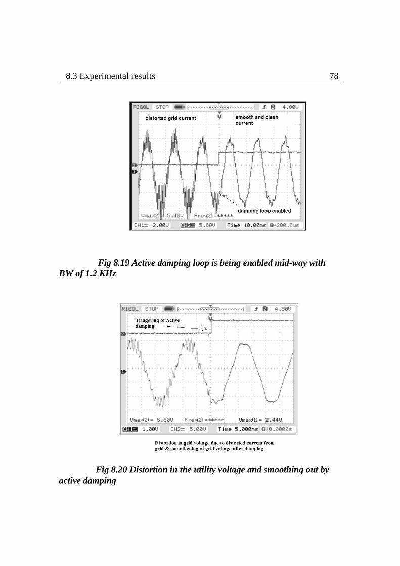
Fig 8.13 Distorted current from grid (full of resonance)
Fig8.14 Less distorted current grid (state-weight age K=10)

8.3 Grid connected mode results 76
Fig 8.15 smooth current from grid (state-weight age 25) and its FFT
Fig 8.16 grid side current dynamics when sudden change in DC-bus

77 Experimental results
Fig 8.17 grid side current dynamics when sudden change load
Fig 8.18 Line side current when active damping is being enabled mid-way
8.3 Experimental results 78
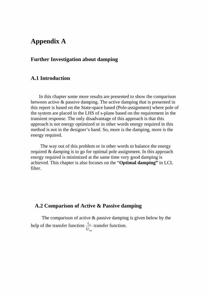
Fig 8.19 Active damping loop is being enabled mid-way with BW of 1.2 KHz
Fig 8.20 Distortion in the utility voltage and smoothing out by active damping

79 Experimental results 8.3 Conclusions The standalone mode results are given in the chapter and those results are enough to prove concepts of controls. The grid connected mode results are very similar to above results with very little difference. It is also clear how state-feedback approach can be very effective for analysis and practical implementation. The analysis is given in chapter 6.

80 8.3 Conclusion
Appendix A Further Investigation about damping A.1 Introduction In this chapter some more results are presented to show the comparison between active & passive damping. The active damping that is presented in this report is based on the State-space based (Pole-assignment) where pole of the system are placed in the LHS of s-plane based on the requirement in the transient response. The only disadvantage of this approach is that this approach is not energy optimized or in other words energy required in this method is not in the designer’s hand. So, more is the damping, more is the energy required. The way out of this problem or in other words to balance the energy required & damping is to go for optimal pole assignment. In this approach energy required is minimized at the same time very good damping is achieved. This chapter is also focuses on the “Optimal damping” in LCL filter. A.2 Comparison of Active & Passive damping The comparison of active & passive damping is given below by the
help of the transfer function 1L
inv
i
Utransfer function.
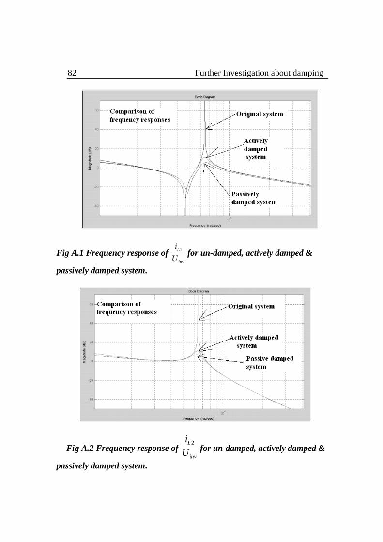
82 Further Investigation about damping
Fig A.1 Frequency response of 1L
inv
i
Ufor un-damped, actively damped &
passively damped system.
Fig A.2 Frequency response of 2L
inv
i
U for un-damped, actively damped &
passively damped system.
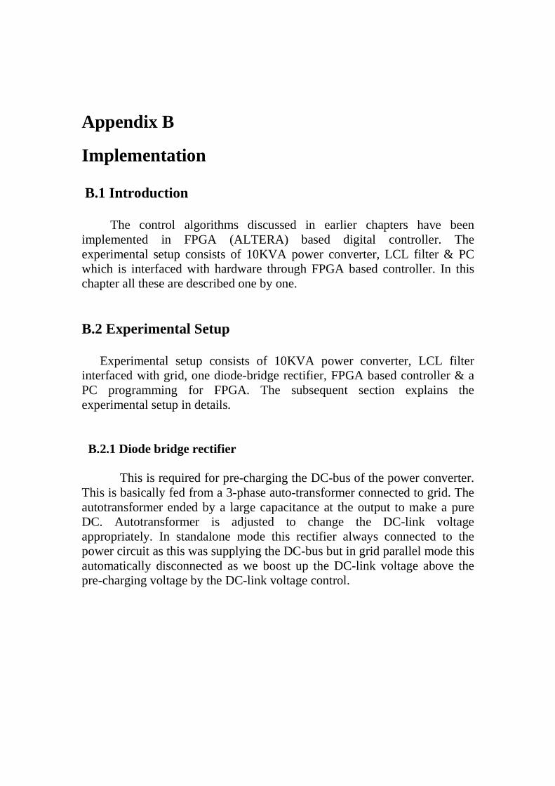
A.3 Optimal Damping (Advanced Active Damping) 83 A.3 Optimal damping (Advanced Active Damping) A.3.1 Introduction The optimal pole is done by solving “Riccati’s Equation”. Here we have complete balance between energy & damping. Linear quadratic (LQ) optimal control gives that freedom to the designer to place pole of the system optimally. In the control law the gain matrix can be found from the Riccati’s Equation. In the LQ based control we can get good stability margin and robustness. In this method we determine the gain matrix ‘K’ after minimizing the cost function. Here the ‘Q’ state weight age matrix and ‘R’ is the input weight age matrix. The ith diagonal of ‘Q’ determine direct weight age and off diagonal element determines the coupling between the states, for the linear system generally these off diagonal terms are not much of importance and are neglected in the current study. A.3.2 Optimal gain matrix calculation There are many ways to select these ‘Q’ and ‘R’ matrices. Here in the present case selection of ‘R’ is pretty simple as grid is not a controllable input hence ‘R’ can be taken as one. But the selection of ‘Q’ is bit controversial. In this design the ‘Q’ is selected by keeping in mind the following criterion.
inv LCLU KX= −
T T
0
1J = (X(t) QX(t) + U (t)RU(t))dt
2
∞
∫

84 Further Investigation about damping
(a) Heavy weight is putted on the L1i so as to get fast and well damped transient response.
(b) Impedance of the capacitor is fairly high @50Hz and very little current bypasses through it also; thus almost similar
weight can be putted on theL2i . (c) cV should be given least weight (or may zero weight) as it
should be directed by the grid voltage in order avoid converter saturation.
By the above criterion Q = and R = 1 Solving the equation, Now system is stable as ‘P’ is positive definite matrix. Now for this ‘P’, optimal gain matrix which is [7 11 2]. The optimal poles are at Here we can see that the gain matrix that is coming is consists of nonzero weight age to all the states unlike in arbitrary pole placement where capacitor weight age was zero.
0 0 0
0 100 0
0 0 50
1 0T TA P PA PBR B P Q−+ − + =
6.5 0.42 2
0.42 0.63 0.1
2 0.1 5.75
P
=
1 TK R B P−=165, 5 15jλ +
−= − −

A.3 Optimal Damping (Advanced Active Damping) 85
Fig A.3 Root loci of the original system & optimally damped system .
Fig A.4 Frequency response of 1L
inv
i
U in the original system &
optimally damped system.

86 Further Investigation about damping
Fig A.5 Frequency response of 2L
inv
i
U in the original system &
optimally damped system. A.4 Conclusion In this chapter the few more comparison of among the different damping procedure is done. The optimal damping seems to be most perfect method of damping as in this method the energy & damping both are balanced but it needs one more sensing of capacitor voltage. Hence this procedure of damping can be applied suitably for sensor less system otherwise system may be complicated & costly also.
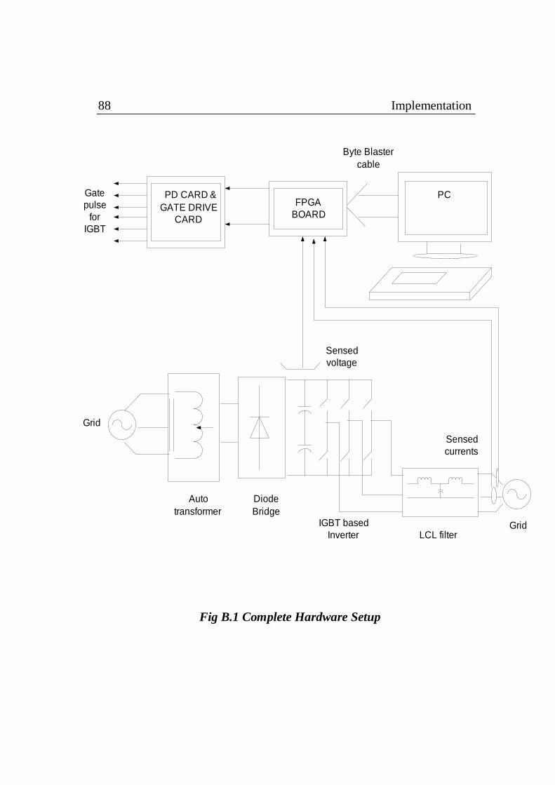
Appendix B
Implementation B.1 Introduction The control algorithms discussed in earlier chapters have been implemented in FPGA (ALTERA) based digital controller. The experimental setup consists of 10KVA power converter, LCL filter & PC which is interfaced with hardware through FPGA based controller. In this chapter all these are described one by one. B.2 Experimental Setup Experimental setup consists of 10KVA power converter, LCL filter interfaced with grid, one diode-bridge rectifier, FPGA based controller & a PC programming for FPGA. The subsequent section explains the experimental setup in details. B.2.1 Diode bridge rectifier This is required for pre-charging the DC-bus of the power converter. This is basically fed from a 3-phase auto-transformer connected to grid. The autotransformer ended by a large capacitance at the output to make a pure DC. Autotransformer is adjusted to change the DC-link voltage appropriately. In standalone mode this rectifier always connected to the power circuit as this was supplying the DC-bus but in grid parallel mode this automatically disconnected as we boost up the DC-link voltage above the pre-charging voltage by the DC-link voltage control.
88 Implementation
PC FPGA
BOARD
PD CARD & GATE DRIVE
CARD
Gate pulse
for IGBT
Sensed currents
Sensed voltage
LCL filterGrid
Grid
Auto transformer
Diode Bridge
IGBT based Inverter
Byte Blastercable
Fig B.1 Complete Hardware Setup
B.2 Experimental setup 89
B.2.2 Pre-charging Autotransformer An auto transformer is placed before the grid & it is used to feeding the inverter DC-link voltage. This facility is used to vary the grid voltage also (we can operate the system at any grid voltage). B.2.3 IGBT based Inverter The power devices are used in the inverter are IGBTs . There are three legs in the inverter with two IGBTs (one module) in each leg. IGBTs are mounted on heat sink & are connected to the DC bus voltage via DC bus bar. The basic components are PD card, Gate drive card, front panel card & sensing cards B.2.4 FPGA Controller The digital platform consists of FPGA device & other devices interfaced to FPGA a shown in A.2. The devices interfaced include configuration device (EEPROM), ADC & DAC; dedicated I/O pins are also provided. The FPGA has logic elements arranged in rows & columns. Each logic elements has certain hardware resources, which will be utilized to realize the user logic. The vertical & horizontal interconnects of varying speeds provide signal interconnects to implement the custom logic. The choice of an FPGA device for a given application is based on the size required (no. of logic elements), clock speed & number of I/O pins. ALTERA EP1CQ240C8 is found to be suitable for the given platform. The resources available in this device are listed in Table.
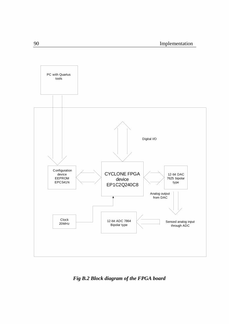
90 Implementation
Configuration device
EEPROM EPCS41N
PC with Quartus tools
CYCLONE FPGA device
EP1C2Q240C8
12-bit DAC7625 bipolar
type
Analog output from DAC
Sensed analog input through ADC
12-bit ADC 7864Bipolar type
Clock 20MHz
Digital I/O
Fig B.2 Block diagram of the FPGA board

\ 8.2 Experimental setup 91
1. Configuration Device
The configuration device is an EEPROM (EPCS41N) which is used to a PC through a parallel port or USB using Byte blaster II or USB blaster cable. The digital design for the implementation of the proposed scheme is done using Quartus-II tool (Altera’s design tool for FPGA) and the output file after compilation is downloaded to EEPROM through Byte blaster II or USB blaster cable.
2. ALTERA FPGA device data Part No EP1C12Q240C8 Manufacturer Altera No. of pins 240 No. of I/O pins 173 Total internal memory bits 2,39,616 Package PQFP No. of logic elements 12000 No. of PLL 2 Maximum clock frequency using PLL
275MHz
3. Analog to Digital converter (ADC)
ADC on the board, AD7864AS-1 of analog devices, is used to convert the analog input signals from the system to digital signals which are used for further processing. This MQFP packaged, 12 bit, 44-pins simultaneous ADC has 4 channels with a conversion time of 1.6 sµ per channel. There are four such ADCs on the board and hence can take up to 16-analog input.

92 Implementation stages
93 Digital to Analog converter (DAC)
DAC on the board, DAC-7625U, is used to output the digital variables in the controller in analog form. The DAC is TTL devices working with +5V and -5V power supply. This is a 12-bit, 28 pins DAC of TEXAS has 4 channels with conversion time of 10sµ .
94 Digital I/Os
Dedicated digital I/Os are necessary to interface to ADC, DAC etc which are present on the board. Apart from that 56 I/O pins are provided for the user to interface application specific hardware.
B.3 Implementation stages The implementation can be done divided into two major parts
(a) Estimation and calculation of different quantities (b) Controller design and realization.
B.4 Conclusion The chapter presented details of the experimental setup & controller used for the purpose. The results of the experiments are given in chapter 8.

93 B.4 Conclusion
References 1. V. Blasko and V. Kaura, “A new mathematical model and control of a three-phase AC-DC voltage source converter,” IEEE Trans. Power Electron., vol. 12, pp. 116–123, Jan. 1997. 2. M. Liserre, F. Blaabjerg, and S. Hansen, “Design and control of an LCL-filter based active rectifier,” in Proc. IAS’01, Sept./Oct. 2001, pp. 299–307. 3. V. Blasko and V. Kaura, “A novel control to actively damp resonance in input lc filter of a three-phase voltage source converter,” IEEE Trans. Ind. Applicat., vol. 33, pp. 542–550, Mar.–Apr. 1997. 4. R. W. Erickson and D. Maksimovic, Fundamentals of Power Electronics. Boston, MA: Kluwer, 2001. 5. M. Liserre, A. Dell’Aquila, and F. Blaabjerg, “Stability improvements of an LCL-filter based three-phase active rectifier,” in Proc. PESC’02, June 2002, pp. 1195–1201.
6. P. A. Dahono, “A control method to damp oscillation in the input LC filter of AC-DC PWM converters,” in Proc. PESC’02, June 2002, pp. 1630–1635. 7. E. Twining and D. G. Holmes, “Grid current regulation of a three-phase voltage source inverter with an LCL input filter,” in Proc. PESC’02, June 2002, pp. 1189–1194.
8. N. Abdel-Rahim and J. E. Quaicoe, “Modeling and analysis of a feedback control strategy for three-phase voltage-source utility interface systems,” in Proc. 29th IAS Annu. Meeting, 1994, pp. 895–902. 9. M. Lindgren and J. Svensson, “Control of a voltage-source converter connected to the grid through an LCL-filter-application to active filtering,” in Proc. Power Electron. Spec. Conf. (PESC’98), Fukuoka, Japan, 1998.

94 References
10. Poh Chiang Loh. “Analysis of Multiloop Control Strategies for LC/CL/LCL-Filtered Voltage-Source and Current-Source Inverters,” IEEE Trans on Industry Applications, 2005, 2(41):644-654. 11. R. Teodorescu, F.Blaabjerg, U. Borup and M.Liserre. “A New Control Structure for Grid-Connected LCL PV Inverters with Zero Steady- State Error and Selective Harmonic Compensation,” APEC, 2004, vol.1: 580-586 12. Hamid R. Karshenas and Hadi Saghafi. “Basic Critia in Designing LCL Filters for Grid Connected Converters,” IEEE ISIE, 2006: 1996-2000 13. F.A. Magueed and J. Svensson, “Control of VSC connected to the grid through LCL-filter to achieve balanced currents,” in Proc. IEEE Industry Applications Society Annual Meeting 2005, vol. 1, pp. 572-8. 14. M. Liserre, A. Dell’Aquila, and F. Blaabjerg, “Genetic algorithm-based design of the active damping for an LCL-filter three-phase active rectifier,” IEEE Transactions on Power Electronics, vol. 19, no. 1, pp. 76-86, 2004. 15. M. Prodanovic and T.C. Green, “Control and filter design of three-phase inverters for high power quality grid connection,” IEEE Transactions on Power Electronics, vol. 18, no. 1, pp. 373-80, 2003. 16. Vector control of three-phase AC/DC front-end converter - J S SIVA PRASAD, TUSHAR BHAVSAR, RAJESH GHOSH and G NARAYANAN. Sadhana Vol. 33, Part 5, October 2008, pp. 591–613. 17. Operation of a three phase - Phase Locked Loop system under distorted utility conditions - Vikram Kaura, Vladimir Blasko. IEEE Transactions 1996.
