review current trends in shrinking the channel...
TRANSCRIPT

REVIE
W
www.advmat.de
20
Current Trends in Shrinking the Channel Length ofOrganic Transistors Down to the Nanoscale
By Yang Cao, Michael L. Steigerwald, Colin Nuckolls, and Xuefeng Guo*
In this Review article, we highlighted current trends in shrinking the channel
length of organic field-effect transistors (OFETs) down to the nanoscale in
three systems where sophisticated device fabrication has been integrated into
the development of different electrodes with nanoscale gaps. The design
principle is the combination of molecular design freedom and flexible
molecular self-assembly with state-of-the-art device fabrication to realize
organic field effect nano-transistors where molecular materials themselves
behave as pivotal elements. Three different types of nanoscale electrodes are
used for OFETs: metals, single-walled carbon nanotubes (SWCNTs), and
graphenes. These electrodes are made by e-beam lithography as well as other
complementary methods (shadow deposition, underetching, nanoimprinting,
rubber stamping, and microcontact printing).
1. Introduction
Rising technical demands ofmodern information society (such ashigh-capacity performance, high-speed capability, high degree ofintegration, and low-power consumption) lead to the pressingneed to scale down the characteristic dimensions of conventionalSi-based optoelectronic devices. The feature size used in Intel andIBM is presently as short as 45 nm, which is well within the‘‘nano’’ range.[1] This trend is expected to continue in the nextdecade. The ultimate goal is the single molecule/atom transistor(Fig. 1).[2–5]
Organic/molecular electronic devices have attracted broadattention over the past decade because of their inherentadvantages, such as solution-processibility, light-weight, thepossibility of large-area processing, low cost, and their flex-ibility.[6–12] Organic field-effect transistors (OFETs), in particular
Figure 1. Illustration of
[*] Prof. X. Guo, Y. CaoCenter for NanochemistryBeijing National Laboratory for Molecular SciencesTate Key Laboratory for Structural Chemistry of Unstable and StableSpeciesCollege of Chemistry and Molecular EngineeringPeking University, Beijing 100871, P. R. (China)E-mail: [email protected]
Prof. C. Nuckolls, Dr. M. L. SteigerwaldDepartment of ChemistryThe Columbia University Center for Electronics of MolecularNanostructuresColumbia University, New York 10027 (USA)
DOI: 10.1002/adma.200900504
� 2010 WILEY-VCH Verlag GmbH & Co. KGaA, Weinheim
as one of the fundamental building blocksof electronic circuits, are one of the mostimportant interests. In general, mostOFETs are built from organic thin filmsas the active layers. Through great efforts inthe past decade the performance character-istics of someOFETs are now comparable tothose of amorphous silicon TFTs.[13] How-ever, the conduction mechanisms in theseorganic thin films are still poorly under-stood. The nature of charge conduction inthin films of organic semiconductors maydiffer from that in bulk organic materials,owing to their sensitivity to the molecularpacking, film morphology, and tempera-ture.[14–17] These factors work together andgreatly influence the quality of organic thin
films. Previous studies have shown that charge transport inOFETs is dominated by defects such as traps and grainboundaries.[18–20] The resulting performance characteristics ofthe devices are significantly limited.
To probe the intrinsic properties of organic thin films, deviceswith defect-free active layers would be necessary. Remarkableattempts have been made to build OTFTs on micro/nanome-ter-scale organic crystals,[21–36] bulk organic crystals,[9,11,12,37,38]
and large single grains.[39] Organic single crystals possessessentially perfect molecular ordering and are virtually free ofgrain boundaries, at least by comparison to the analogous organicthin films. The effective use of organic single crystals can affordmicro/nanometer-sized organic single-crystalline transistors.However, it is a big challenge to design molecules thatself-assemble in a predictive manner via weak Van der Waalsforces into ordered high-quality single crystals over a large areaand in a controllable way.[10,22,23,38] More work directed towardimproving the performance of these devices is needed. Anotherimportant approach to minimizing defect density is to shrink theactive channels by aggressively scaling down OFETs. From theview of the practical application, this approach is more usefulsince device miniaturization could make tremendous contribu-tion to the integration of future optoelectronic circuits.[3,4]
Shrinking device dimensions down to molecular length scalesof organic semiconductors offers new, defect-free charge
a single molecule/atom transistor.
Adv. Mater. 2010, 22, 20–32

REVIE
W
www.advmat.de
Yang Cao received her B.Sc. in Chemistryfrom Zhengzhou University, China in2007. She is currently pursuing a Ph.D. atthe College of Chemistry and MolecularEngineering, Peking University at Beij-ing, China under the guidance ofXuefeng Guo and Zhongfan Liu. Hercurrent research is focused on molecularelectronic devices based on graphene.
Xuefeng Guo received his Ph.D. in 2004from the Institute of Chemistry, ChineseAcademy of Science, Beijing, withDaobenZhu and Deqing Zhang. From 2004 to2007, he was a postdoctoral scientist atColumbia University with Colin Nuckollsand Philip Kim. He joined the faculty atPeking University in 2008. His researchfocuses on functional nanometer/mole-cular devices.
transport regimes. This may lead to larger carrier mobilities,increased device speed, and enhanced ON/OFF ratio. Scalingdown OFETs implies the reduction of the device dimensions,both the thickness of the devices (the semiconductor and/orinsulator layers) and their lateral dimension (source–draindistance). Several attempts to reduce the semiconductor/insulator thickness have been made using Langmuir–Blodgett(LB) films[40–42] and self-assemblied monolayer (SAMs) or
Table 1. Device characteristics of OFETs with nanoscale channel lengths.
Parameters
publications
m (cm2/Vs) L (nm) tox (nm) VD (V) VG (V) ON/O
rat
Collet et al. [60] – 250 2 1.0 �1 10
Rogers et al. [72] 1� 10�3 100 20 �5 �3 25
Collet et al. [61] 3.6� 10�4 30 2 �1.5 �1.5 <1
Granstorm et al. [64] 5� 10�4 400 150 �10 �30 10
Chwang et al. [65] 10�4 500 150 �15 �15 10
Jones et al. [68] – 50 100 0.1 0.4 –
Austin et al. [70] 8� 10�4 70 5 �3 �3 10
Zaumseil et al. [71] – 150 26 �2 �2.2 <1
Wang et al. [66] 0.046 9 100 �5 �30 10
Zhang et al. [62] 0.01 30 30 �2 �4 10
Scheinert et al. [69] 3� 10�5 700 50 �5 �5 10
Tulevski et al. [56] – 40 10 �3 �2.5 10
Qi et al. [79] – 6 10 �1 �3 10
Tsukagoshi et al. [78] – <500 200 �2 �10 10
Lee et al. [63] – 10 3 �0.3 �0.3 10
Tulevshi et al. [55] 0.022 40–100 5 �3.6 �3.6 10
Guo et al. [54] �l [a] <10 300 �20 �20 10
Mottaghi et al. [57] 0.0035 50–1000 100 �0.5 �3 1.8�Smits et al. [58] 0.01 750 200 �20 �20 10
Guo et al. [80] �l [a] <10 300 �20 �20 10
Cao et al. [81] 10�3 100 300 �20 �5 10
[a] This mobility is only for comparison with other thin film transistors because it assu
[b] Contorted hexabenzocoronene.
Adv. Mater. 2010, 22, 20–32 � 2010 WILEY-VCH Verlag Gmb
multilayers.[43–61] These studies utilized sophisticated molecularassemblies that spontaneously happen when the substrates aredipped sequentially into solutions of the active components toform an active part of OFETs, either the gate dielec-tric[44–46,49,51,52,60,61] or the semiconductor layer.[54,56–58] In theformer case, OFETs built on self-assemblied gate dielectric layerscan function at a very low-operating voltage (as small as 2V). Thisapproach is attractive because it increases the capacitive couplingthrough the gate insulators and thus reduces the powerdissipation. The big challenge, however, is to build moleculargate dielectric layers that minimize gate leakage currents. In thelatter case, the electrical characteristics of the devices do not allowclear parameter extraction (in most cases) due to the inherentproblems in the devices (such as the contact resistance and poorintermolecular p–p stacking between molecules in the self-assemblied layers). It is possible to realize large-area SAM fieldeffect transistors (FETs) if densely packed SAMs can be achieved.This possibility has been well demonstrated by the recent work byEdsger C. P. Smits et al.[58]
In this Review article, we will describe the current trends inshrinking the channel length of organic transistors down to thenanoscale in three systems in order to minimize defect density inthe device materials. In each system sophisticated devicefabrication is integrated into the development of differentnanoscale electrodes. The incorporation of molecular self-assembly into the device fabrication allows us to build effectivefield effect nano-transistors. These three systems are i) nanoscalemetal electrodes (made using electron beam (e-beam) lithogra-phy,[55–57,60–67] shadow deposition,[68] underetching,[69] nanoim-printing,[70] rubber stamping,[71] and microcontact printing,[72]),ii) single-walled carbon nanotube (SWCNT) electrodes,[5,54,73–79]
FF
io
S mV/Dec Current
saturation?
Materials Fabrication Method Year
300 n n-Si E-beam lithography 1998
– y sexithiophene Microcontact printing 1999
0 350 n sexithiophene E-beam lithography 2000
0 – n sexithiophene E-beam lithography 1999
0 – n sexithiophene E-beam lithography 2000
– – polyaniline Shadow deposition 19874 – n P3HT Nanoimprinting 2002
00 – n Pentacene Rubber stamping 2003
0 – n Pentacene E-beam lithography 2004
0 – y Pentacene E-beam lithography 20034 400 n P3HT Underetching 2004
– n Tetracene E-beam lithography 20043 400 n Pentacne, P3HT E-beam lithography 20043 – n Pentacene E-beam lithography 2004
0 – y Pentacene E-beam lithography 20053 – y Pentacene E-beam lithography 20063 500 y HBC [b] E-beam lithography 2006
l03 – n Oligothiophene E-beam lithography 20076 – y Oligothiophene Photolithography 20083 500 y HBC [b] E-beam lithography 20095 20 V/Dec n Pentacene, P3HT E-beam lithography 2009
mes a parallel capacitor model for the gate dielectric, which is not accurate here.
H & Co. KGaA, Weinheim 21

REVIE
W
www.advmat.de
Figure 2. A) A possible leakage path that would allow for transistor actionwithout the current actually passing through the nanogap. Reproducedwith permission from [63]. Copyright 2005, IEEE. B) The function of the twoside guards is to suppress fringe currents. The white scale bar is 100 nm.Reproduced with permission from [66]. Copyright 2004, American Instituteof Physics.
22
and iii) cut single-layer graphene sheets as 2D contacts.[81] We willdescribe the fabrication of these devices as well as some of theirunique characteristics and sensitivities.
2. OFETs Based on Nanoscale Metal Electrodes
Traditionally, Si-based devices are made with metal electrodes,such as Au, Cu, and Pt, because of their high conductivities andtheir compatibility with industrial semiconductor processes.With great effort numerous approaches have been used to makenanoscale metal electrodes in order to achieve OFETs withsubmicrometer channel length. These methods include e-beamlithography,[55–57,60–67] shadow deposition,[68] underetching,[69]
nanoimprinting,[70] rubber stamping,[71] and microcontact print-ing.[72] Device characteristics of OFETs made by each method arelisted in Table 1. These results are promising and in principledemonstrate the possibility of realizing functional OFETs withchannel lengths in the nanometer range and the wide capabilityfor application in nanoscale/molecular electronics.
2.1. E-beam Lithographic Method
E-beam lithography is the most commonly used technique tofabricate nanoscale metal electrodes. OFETs with sub 100 nmchannel lengths have been reported. For example, by usinge-beam lithography and lift-off techniques, Collet[60,61] and Zhang
Figure 3. a) Molecular structure of an end functionalized tetracene and schematic of bondingand orientation of it on aluminum oxide. b) SEM image of the nanodevices. c) SEM image of the40 nm gap. d) Source–drain I/V curves at different gate biases [GV¼ 0 (red) to �2.5 V (darkgreen) in �0.5 steps]. Inset: Tapping mode AFM image of the 40 nm device. Reproduced withpermission from [56]. Copyright 2004, ACS.
et al.[62] have reported the fabrication of organicthin-film transistors with a channel length asshort as 30 nm. OFETs with even smallerchannel lengths (10 nm) were also fabricatedby Subramanian’s group.[63] However, in suchdevices with small W/L ratio, a significantportion of the measured drain current mayactually result from fringe current ratherchannel current, through the path illustratedin Figure 2. To suppress spreading current indevices, Wang et al.[66] employed a new pair ofguarding electrodes, which are as close as20 nm to the two sides of the channel (Fig. 2B),to improve the FETproperties of pentacene thinfilm transistors with sub 10 nm channellengths. Such OFETs based on nanoscale metalelectrodes are very interesting for studyingthe intrinsic properties of organic thin films,and they can operate at low voltage (Table 1).Their current–voltage characteristics exhibit
� 2010 WILEY-VCH Verlag Gm
the similar p-type FET behaviors. Typical field-effect mobilitiesof these nanodevices are the order of 10�2 cm2 V�1 s�1 (Table 1).At this early stage these studies show that it is possible to realizefunctioning OFETs with the channel length down to thenanoscale, and that their electrical characteristics exhibit goodperformance, comparable to macroscopic OFETs.
Previous reports of organic thin-film devices have shown thatthe first few molecular layers of organic semiconductor at theoxide interface are the locus of charge injection and areresponsible for current modulation.[14,43,44,64,65] It is veryimportant to explore the subtle correlation between structures,assemblies, and properties of the first layer of organicsemiconductors. Little work has been devoted to the use of thefirst layer or self-assembled monolayer (SAM) as an active part ofOFETs due to the great challenge of achieving uniform SAMswith dense packing. Recently, Tulevski et al.[56] demonstrated anew class of organic semiconductor that spontaneously formsupright monolayers on gate oxides. They found that a tetracenederivative covalently forms dense, upright monolayers on thesurface of the aluminum oxide dielectric layer (Fig. 3A). The rigid,covalent attachment provides a direct method for using thedielectric surface structure as an adjustable parameter to tune themonolayers’ self-assembled structure and therefore their elec-trical properties. After these monolayers spontaneously self-organize into the active layer in nanoscale field-effect transistor(FET) devices with prepatterned source–drain electrodes sepa-rated by less than 100 nm (Fig. 3B, C), the resulting devicesshowed the p-type, hole transporting properties (Fig. 3D). Thiswork opens up a new avenue for studying the intrinsicproperties of SAM as the active layer in nanoscale thin-filmorganic transistors. Moreover, the SAM-based nanodevicescould act as highly sensitive environmental and molecularsensors since the first layer of the active channel is exposed to theenvironment.
As the authors mentioned, this work still suffers from twofactors: one is the sharp decrease in the yield of the devices withl> 60 nm, and the other is the nonlinear I/V curves and thefailure of the current saturation (Fig. 3D). These issues can beascribed to the problems of poor long-range organization of
bH & Co. KGaA, Weinheim Adv. Mater. 2010, 22, 20–32
REVIE
W
www.advmat.de
the organic monolayer, poor charge injection from contacts, andincreased contact resistance. However, the recent work byMottaghi[57] and Zhang et al.[62] demonstrated sub 100 nmOFETs which do show saturated current output currents,indicating that these observed nonidealities may not be intrinsicto nanoscale OFETs. In Mottaghi’s work OFETs are built on anSAM formed from bifunctional molecules comprising a shortalkyl chain linked to an oligothiophene moiety that acts as theactive semiconductor.[57] Platinum/titanium source and drainelectrodes are patterned by e-beam lithography, with a channellength ranging between 20 and 1000 nm. Although ill-defined I/Vcurves were recorded, attributed to a poor electrical contactbetween platinum and the oligothiophene moiety in most cases, afew devices did offer well-defined curves with a clear saturation.
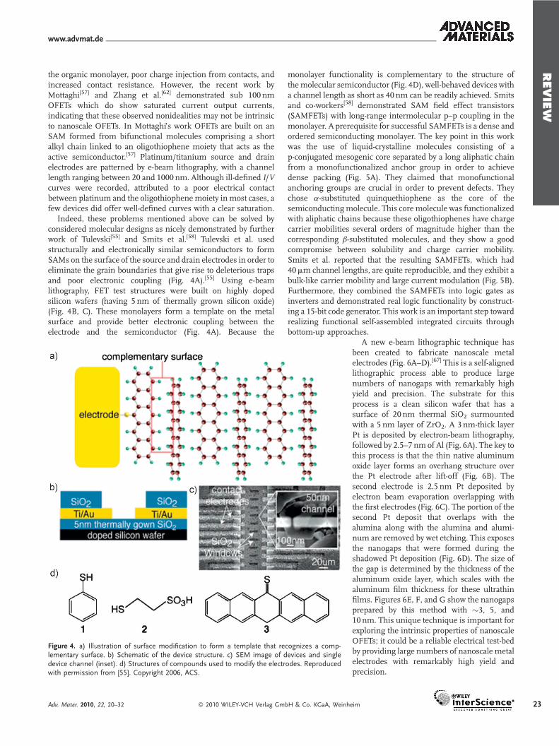
Indeed, these problems mentioned above can be solved byconsidered molecular designs as nicely demonstrated by furtherwork of Tulevski[55] and Smits et al.[58] Tulevski et al. usedstructurally and electronically similar semiconductors to formSAMs on the surface of the source and drain electrodes in order toeliminate the grain boundaries that give rise to deleterious trapsand poor electronic coupling (Fig. 4A).[55] Using e-beamlithography, FET test structures were built on highly dopedsilicon wafers (having 5 nm of thermally grown silicon oxide)(Fig. 4B, C). These monolayers form a template on the metalsurface and provide better electronic coupling between theelectrode and the semiconductor (Fig. 4A). Because the
Figure 4. a) Illustration of surface modification to form a template that relementary surface. b) Schematic of the device structure. c) SEM image of ddevice channel (inset). d) Structures of compounds used to modify the electrwith permission from [55]. Copyright 2006, ACS.
Adv. Mater. 2010, 22, 20–32 � 2010 WILEY-VCH Verlag Gmb
monolayer functionality is complementary to the structure ofthemolecular semiconductor (Fig. 4D), well-behaved devices witha channel length as short as 40 nm can be readily achieved. Smitsand co-workers[58] demonstrated SAM field effect transistors(SAMFETs) with long-range intermolecular p–p coupling in themonolayer. A prerequisite for successful SAMFETs is a dense andordered semiconducting monolayer. The key point in this workwas the use of liquid-crystalline molecules consisting of ap-conjugated mesogenic core separated by a long aliphatic chainfrom a monofunctionalized anchor group in order to achievedense packing (Fig. 5A). They claimed that monofunctionalanchoring groups are crucial in order to prevent defects. Theychose a-substituted quinquethiophene as the core of thesemiconductingmolecule. This core molecule was functionalizedwith aliphatic chains because these oligothiophenes have chargecarrier mobilities several orders of magnitude higher than thecorresponding b-substituted molecules, and they show a goodcompromise between solubility and charge carrier mobility.Smits et al. reported that the resulting SAMFETs, which had40mm channel lengths, are quite reproducible, and they exhibit abulk-like carrier mobility and large current modulation (Fig. 5B).Furthermore, they combined the SAMFETs into logic gates asinverters and demonstrated real logic functionality by construct-ing a 15-bit code generator. This work is an important step towardrealizing functional self-assembled integrated circuits throughbottom-up approaches.
cognizes a comp-evices and singleodes. Reproduced
H & Co. KGaA, Weinh
A new e-beam lithographic technique hasbeen created to fabricate nanoscale metalelectrodes (Fig. 6A–D).[67] This is a self-alignedlithographic process able to produce largenumbers of nanogaps with remarkably highyield and precision. The substrate for thisprocess is a clean silicon wafer that has asurface of 20 nm thermal SiO2 surmountedwith a 5 nm layer of ZrO2. A 3 nm-thick layerPt is deposited by electron-beam lithography,followed by 2.5–7 nm of Al (Fig. 6A). The key tothis process is that the thin native aluminumoxide layer forms an overhang structure overthe Pt electrode after lift-off (Fig. 6B). Thesecond electrode is 2.5 nm Pt deposited byelectron beam evaporation overlapping withthe first electrodes (Fig. 6C). The portion of thesecond Pt deposit that overlaps with thealumina along with the alumina and alumi-num are removed by wet etching. This exposesthe nanogaps that were formed during theshadowed Pt deposition (Fig. 6D). The size ofthe gap is determined by the thickness of thealuminum oxide layer, which scales with thealuminum film thickness for these ultrathinfilms. Figures 6E, F, and G show the nanogapsprepared by this method with �3, 5, and10 nm. This unique technique is important forexploring the intrinsic properties of nanoscaleOFETs; it could be a reliable electrical test-bedby providing large numbers of nanoscale metalelectrodes with remarkably high yield andprecision.
eim 23

REVIE
W
www.advmat.de
Figure 5. a) X-ray reflectivity (XRR) of the SAM on silicon dioxide. The solid red line is the fit to the experimental data. The inset shows the chemicalstructure of themolecule and the thicknesses, root-mean-square (r.m.s.) roughness values and electron densities obtained from the fit. The measurementsreveal a layer thickness equivalent to one monolayer. b) Output characteristics for the corresponding SAMFET. The gate voltage was varied from �5 to�20 V in steps of �5 V. Reproduced with permission from[58]. Copyright 2008, Nature Publishing Group.
24
2.2. Other Methods
In addition to e-beam lithography, a large number of approacheshave been developed to make nanoscale metal electrodes in orderto achieve OFETs with submicrometer channel lengths. Forexample, Wrighton and co-workers[68] used multistep shadowdeposition techniques to prepare molecule-based transistors withthe source–drain electrodes separated by 50 nm (Fig. 7A). Rogerset al.[72] integrated near-field photolithography with microcontactprinting and shadow masking to demonstrate complementaryinverter circuits from OFETs with 100 nm channel length.Scheinert et al.[69] developed an underetching technique to definesubmicrometer channel length polymer FETs (Fig. 7B). Thetransistors with submicrometer channel length show theoperating voltage as low as 5V with a low inverse subthreshold
Figure 6. a) A line of Al on Pt is deposited by e-beam lithography on a siliconZrO2. b) Air in the ambient oxidizes aluminum to produce an overhanging alumc) Evaporation of the counter electrode produces platinum separated byaluminum oxide overhang. d) Dissolving the aluminum/aluminum oxide lspaced platinum electrodes. e) SEM showing a 3 nm gap; the part in the red rec200%. F) SEM showing a 5 nm gap. G) SEM showing a 10 nm gap. Reproducedfrom ref. [67]. Copyright 2007, Wiley-VCH.
� 2010 WILEY-VCH Verlag Gm
slope of 0.4–0.5 V/dec, on–off ratio of 104, and withoutshort-channel effects. Austin and Chou[70] successfully fabricated70 nm channel length polythiophene transistors using nanoprint-ing lithography (Fig. 7C). Finally, Zaumseil et al.[71] used ahigh-resolution rubber stamping technique to define channelsdown to 150 nm and built pentacene transistors (Fig. 7D). Thegood performance of all the devices and their low-voltageoperationmake them and the fabrication procedures attractive formany applications.
3. OFETs Based on SWCNT Electrodes
Since their discovery,[82] carbon nanotubes have been regarded asone of the best nanostructural materials derived from bottom-upchemical synthesis.[3,4] Carbon nanotubes have the simplest
wafer coated withinum oxide layer.the amount of
ayer give closelytangle is enlargedwith permission
bH & Co. KGaA, Wei
chemical composition and atomic bondingconfiguration but exhibit perhaps the mostextreme diversity and richness among nanoma-terials in structures and structure–propertyrelations.[83,84] SWCNTs are 1D ballisticallyconducting nanowires that are intrinsically thesamescaleasmolecules.Theyareeasy toprocessfor nanofabrication. SWCNTs are formed byfoldingup a graphene sheet into a cylinder alonga certain lattice vector. This hints at usefulconduction via the p-bonding network. Ulti-mately SWCNTs are composed of carbonsix-membered rings, and therefore we proposethat a high-quality contact can be formedbetween SWCNT electrodes and molecules. Asa result of all of these features, SWCNTs shouldbe ideal point contacts for testing the intrinsicproperties of various molecular devices withmolecular sizes in all dimensions.[5,54,73–79]
We form SWCNTelectrodes by cutting themby precise local oxidation through a poly-methylmethacrylate (PMMA) mask.[73] Themask is created by e-beam lithography. Thisprocess leaves two ends that are separated by a
nheim Adv. Mater. 2010, 22, 20–32

REVIE
W
www.advmat.de
Figure 7. Schematic illustrations of building thin film transistors by multistep shadow mask technique a), underetching lithography b), nanoprintinglithography c), and rubber stamping technique d). Reproduced with permission from [68–71]. Copyright 1987, ACS, and copyright 2004, 2002, and 2003,AIP, respectively.
gap of �10 nm (Fig. 8A, B). This method differs from theformation of SWCNT electrodes by electrical breakdown, whichhas been used recently to realize pentacene nanotransistors by Qiand Tsukagoshi et al.[78,79] In both cases, applying a high currentthrough the channel disconnected each single-walled or multi-walled carbon nanotube that bridged the twometal leads. Organicmaterials were then thermally evaporated to bridge the gap. Thisformed ultra small OFETs having nanoscale channel lengths(Fig. 8). These two studies have proven that carbon nanotubes canbe novel electrodes for a variety of molecular devices.
In order to fabricate SWCNTelectrodes we prepare an array ofSWCNT transistors and spin-coat this array with a blanket layer ofPMMA. Then we open a window (<10 nm) on top of individualSWCNT transistors using ultra high-resolution e-beam litho-graphy. We then cut the nanotubes through the window viaoxygen plasma ion etching (Fig. 9A, B). We control the degree ofcutting, and therefore the gap size, by varying the time of the
Figure 8. Individual carbon nanotubes as electrodes for small OFETs. A) Schecut SWCNT with a sub-10-nm gap to be used as source (S) and drain (D) electrFET and AFM image of a cut SWNT with a vapor-deposited pentacene crystaSWNT. B) Cross-sectional view of device structures of the pentacene nanotrannanotube electrodes. Reproduced with permission from [78–79]. Copyrighcopyright 2004, AIP, respectively.
Adv. Mater. 2010, 22, 20–32 � 2010 WILEY-VCH Verlag Gmb
exposure to the oxidant. Figure 9C shows an AFM image of onenanogap. Given the imaging convolution of the AFM tip size, anupper bound on the size of a typical gap in these micrographs is�10 nm. This strategy allows molecules to be wired into theSWCNT circuits through robust amide linkages, avoiding thecommon problems related to thiol molecules inserted betweengold electrodes. The amide linkages are so robust that the devicescan endure external stimuli and chemical treatments. Utilizingthis method, we have tested a number of different types ofmolecular wires.[73–77] We have made different types of molecularelectronic devices that are able to switch conductance as afunction of pH,[73] detect the binding between protein andsubstrate,[76] photoswitch the conductance between conjugatedand nonconjugated states,[77] and measure the conductancedifferences between complementary and mismatched DNAstrands.[74] Detailed below are the new applications of thisstrategy in organic electronics. We have demonstrated that
matic drawing of aodes of an organicllite bridging a cutsistor with carbont 2004, ACS, and
H & Co. KGaA, Weinh
SWCNTs can function as efficient pointcontacts for nanoscale FETs. We made FETsout of both monolayers[54] and self-assembledcolumns[80] of polycyclic aromatic hydrocar-bons. These devices are ultrasensitive to theirchemical environment, temperature, andlight.[54,80]
3.1. Chemoresponsive Monolayer
Transistors
It is a formidable challenge to make organicmonolayer transistors because when thesemiconducting layers of typical OFETs arescaled down to a monolayer their properties
eim 25

REVIE
W
www.advmat.de
Figure 9. A) Very fine cutting of SWCNTs with oxygen plasma introduced through an opening ina window of PMMA defined with e-beam lithography. B) The results of oxidative opening of thetubes are point-contacts that are functionalized on their ends and separated by as little as�2 nm. C) AFM image of the gap cut into the SWCNT. Inset: height profile of the isolated tubes.Reproduced with permission from [73]. Copyright 2006, American Association for the Advance-ment of Science.
26
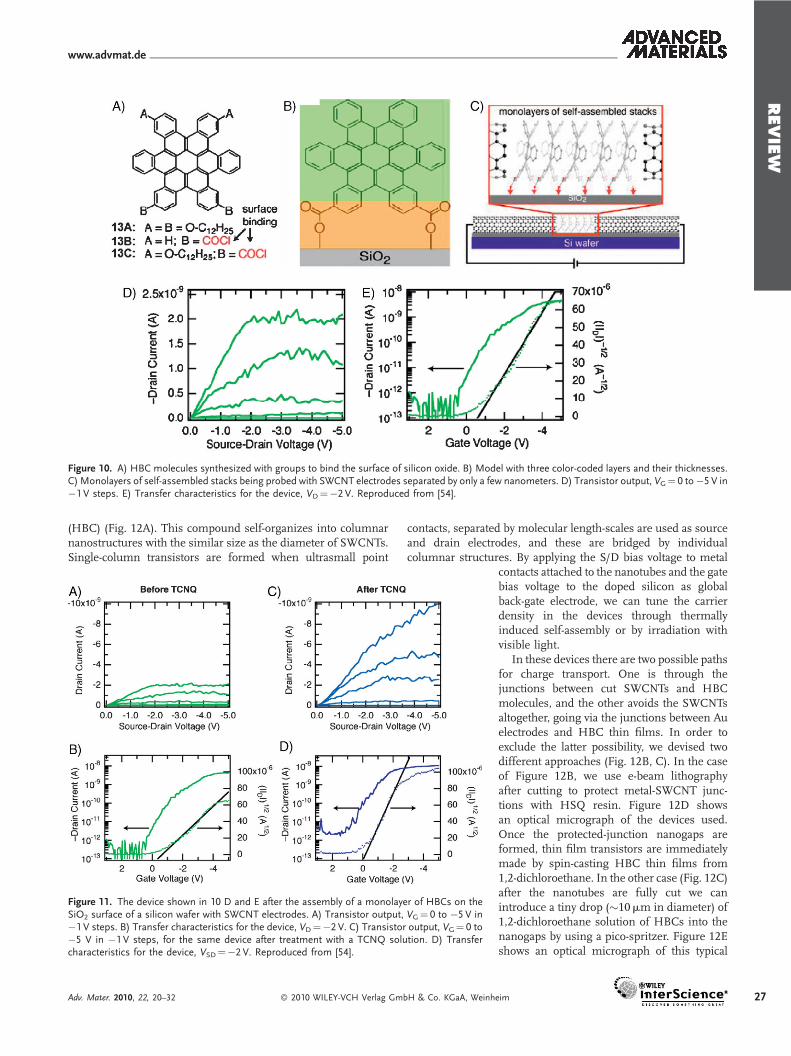
generally become poor, presumably due to discontinuities ordefects in the films.[54,56–58] However, this problem could becircumvented by chemically functionalizing the molecularsemiconducting material such that the molecules both assemblelaterally and attach themselves chemically to the substrate(Fig. 10).[54] We have found that monolayers of molecules behaveas p-type semiconductors when they are incorporated into FETswired by SWCNTelectrodes. The devices show both large currentmodulation and high gate efficiency. Contorted hexabenzocor-onenes (HBCs) (Fig. 10A) were chosen because these compoundsself-organize into molecular stacks with useful semiconductingproperties. Acid chloride functionality was chosen for itswell-known ability to bind to the silicon oxide surface. Owingto their good solubility, high-coverage monolayers with �0.7molecules per square nm on silicon oxide can be easily formed.The surface reaction between the carbonyl chlorides of the HBCsand the oxygens of the silicon oxide produces an ester, impartingsignificant stability to the monolayers (Fig. 10B). Surface X-rayreflectivity data can be fit well to a box-model of three layers(Fig. 10B), which implies an HBC monolayer, composed of anester layer and the HBC core, whose thickness is approximately12.2 A. These reflectivity results are in agreement with the resultsfrom UV-vis absorption that show that the molecules of themonolayer are essentially upright and tightly packed on thesilicon oxide surface. Another striking feature of the X-rayscattering is the extremely high electron density (0.54 e�/A3) forthe HBC layer. The tight packing of these molecules and their
� 2010 WILEY-VCH Verlag GmbH & Co. KGaA, Wei
high p-electron density imply useful electronicproperties of the monolayer. To aid in thesubsequent analysis of the devices, we only usethose that are wired using metallic SWCNTs.
When ultra-small point contacts, separatedby molecular length-scales, are used as thesource and drain electrodes (Fig. 10C), transis-tors can be made from monolayers of thesemolecules. These transistors have high gateefficiency and large ON/OFF ratios. Theseelectrically active monolayers of HBCs behaveas p-type semiconducting films. Figure 10Dand E show the transistor characteristics for amonolayer of HBCs. These devices are verystable; they can be cycled many times despitethe high levels of current through theseself-assembled stacks. The carrier mobility isvery high (�1 cm2 V�1 � s�1). In such a deviceusing SWCNT S/D electrodes separated by�10 nm, owing to their 1D nature, the electricfield from the back gate could focus on theSWCNT junction regions and efficiently pene-trate into the middle of the semiconductorchannel, thus leading to the observed high gatemodulation. Another possibility is that thegate voltage does change the properties of thecontact. However, it is logically very difficult toseparate the behavior of the contact from thebehavior of the semiconductor, since the devicemust be a combination of the two (plus the otherelements: the dielectric, etc.). We suppose thatthe synergistic effects of surface attachment of
HBCmolecules, the upright conformation, the close packing, andthe particular 1D nature of SWCNT electrodes produce thehigh-performance FET behavior. This study demonstrates a clearexample of how the ever-reducing dimensions of top-down devicefabrication can be tailored to mesh with the expanding lengthscales of bottom up self-assembly.
Since the electrical current in OFETs travels through the firstfew layers of molecules near the oxide interface, these monolayerdevices can detect certain types of molecules. In other words, theactive channel of such a monolayer device is exposed to theenvironment and is available for analyte recognition. Figure 11shows the transistor characteristics for the device shown inFigure 10D and E after dipping into a solution of the well-knownelectron acceptor TCNQ. Given the affinity of TCNQ for themolecules such as coronene, it likely acts as a dopant for thestacks by accepting p-electrons. This would explain the shift involtage threshold to more positive values and the increase of theOFF-current by roughly an order of magnitude. These resultsform the basis for a new type of environmental and molecularsensors. What is left unclear is how this doping occurs: whether itis through an intercalation of the TCNQ or some other associativemechanism.
3.2. Photoresponsive Nanoscale Columnar Transistors
In order to make the photoresponsive transistors[80] we used theliquid crystalline material tetra(dodecyloxy)hexabenzocoronene
nheim Adv. Mater. 2010, 22, 20–32
REVIE
W
www.advmat.de
Figure 10. A) HBC molecules synthesized with groups to bind the surface of silicon oxide. B) Model with three color-coded layers and their thicknesses.C) Monolayers of self-assembled stacks being probed with SWCNT electrodes separated by only a few nanometers. D) Transistor output, VG¼ 0 to�5 V in�1 V steps. E) Transfer characteristics for the device, VD¼�2 V. Reproduced from [54].
(HBC) (Fig. 12A). This compound self-organizes into columnarnanostructures with the similar size as the diameter of SWCNTs.Single-column transistors are formed when ultrasmall point
Figure 11. The device shown in 10 D and E after the assembly of a monolayeSiO2 surface of a silicon wafer with SWCNT electrodes. A) Transistor output,�1 V steps. B) Transfer characteristics for the device, VD¼�2 V. C) Transistor�5 V in �1 V steps, for the same device after treatment with a TCNQ solucharacteristics for the device, VSD¼�2 V. Reproduced from [54].
Adv. Mater. 2010, 22, 20–32 � 2010 WILEY-VCH Verlag Gmb
contacts, separated by molecular length-scales are used as sourceand drain electrodes, and these are bridged by individualcolumnar structures. By applying the S/D bias voltage to metal
r of HBCs on theVG¼ 0 to �5 V inoutput, VG¼ 0 totion. D) Transfer
H & Co. KGaA, Weinh
contacts attached to the nanotubes and the gatebias voltage to the doped silicon as globalback-gate electrode, we can tune the carrierdensity in the devices through thermallyinduced self-assembly or by irradiation withvisible light.
In these devices there are two possible pathsfor charge transport. One is through thejunctions between cut SWCNTs and HBCmolecules, and the other avoids the SWCNTsaltogether, going via the junctions between Auelectrodes and HBC thin films. In order toexclude the latter possibility, we devised twodifferent approaches (Fig. 12B, C). In the caseof Figure 12B, we use e-beam lithographyafter cutting to protect metal-SWCNT junc-tions with HSQ resin. Figure 12D showsan optical micrograph of the devices used.Once the protected-junction nanogaps areformed, thin film transistors are immediatelymade by spin-casting HBC thin films from1,2-dichloroethane. In the other case (Fig. 12C)after the nanotubes are fully cut we canintroduce a tiny drop (�10mm in diameter) of1,2-dichloroethane solution of HBCs into thenanogaps by using a pico-spritzer. Figure 12Eshows an optical micrograph of this typical
eim 27

REVIE
W
www.advmat.de
Figure 12. A schematic of how HBCs can be assembled to form single-column transistors andmeasured by SWCNT point contacts. A) The structure of contorted liquid crystalline tetra(dodecyloxy)hexabenzocoronene (HBC). B) Device structure of single column transistors withSWCNT-metal junctions protected by HSQ. C) Device structure of single column transistorsmade by drop-casting. Only the nanogaps between SWCNT electrodes are covered by HBCs.D) An optical microscopy image of a device whose SWCNT-metal junctions have been protectedby HSQ. E) An optical microscopy image of a device produced by drop-casting HBCs exactly onthe nanogaps. Reproduced from [80].
28
device structure. It is very clear that the tiny drop of organicsemiconducting materials is not connected to any metalelectrode. In both of the cases charge exclusively passes throughSWCNT-molecule-SWCNT junctions, identifying that thesenanojunctions play a key role in the electronic characteristicsof the devices.
It is noteworthy that the electrical properties of these devicesimprove significantly after annealing. Before the devices were
Figure 13. Device characteristics of a device before and after annealing. A) Transistor output,VG¼ 0 to �3 V in �0.6 V steps. (B) Transfer characteristics for the device, VD¼�3 V.C) Transistor output, VG¼ 0 to �11 V in �2.2 V steps for the same device after the treatmentof heat. B) Transfer charateristics for the device, VD¼�11V. Reproduced from [80].
� 2010 WILEY-VCH Verlag GmbH & Co. KGaA, Wein
annealed, we found that the yield of theworking devices was low (�10%) and themaximum current within the measured scaleis quite small as shown in Figure 13A, B, whileafter heating the yield of the working devicesincreased to �60%. Another significant dif-ference is the maximum current after anneal-ing, which increased by a factor of over twoorders at VD¼�3V (Fig. 13C, D). Thesemolecular transistors, which have the 1Dballistic SWCNTs as point contacts, exhibithigh-current modulation and a high ON/OFFratio. The ON/OFF ratio is as high as 103; thisis difficult to achieve in ultrasmall devices withmetallic S/D electrodes. This is because of thesynergistic effects of the 1D nature of SWCNTelectrodes in the devices and self-assembliedcolumnar nanostructures of HBCs.
Another significant advantage is that we canuse SWCNTs as point contacts to measure thephotoconductivity of an individual, 1D liquidcrystalline columnar core. This is because thesize of these columnar nanostructures per-fectly matches the diameter of SWCNT
electrodes. In Figure 14A and B we compare the electricalcharacteristics of the same annealed device made by drop-castingin the dark and under the irradiation of visible light. Themeasured photoconductivity originates from photoexcitationsthat are restricted in the 1D hexaradialene-core by theinsulating alkoxyphenyl cladding. When the devices are held atfixed source-drain bias and gate bias by switching on/off light, thereversible photocurrent of the devices can be monitored in the
real time (Fig. 14C). We also found that thedevice photoresponsiveness is universal sincewe used another organic semiconductor(dithiophenylpentacene) to observe the similarphenomenon. These studies demonstrate thatefficacious stimuli-responsive single columntransistors should have the potential forapplications in ultrasensitive devices forenvironmental sensing and solar energyharvesting.
4. OFETs Based on 2D GrapheneElectrodes
Graphene, a newly isolated form of car-bon,[85,86] has a set of remarkable electronicand physical properties that make them idealfor use in nanoelectronics[87–89] and itsdiscovery has led to a flood of worldwideresearch interest.[90–99] As an electrode fornanoscale electrical devices graphene is attrac-tive because it is a very thin (single-atom thick),two-dimensional semimetal that is easilyavailable in very high crystallographic quality.We suggest that graphene may prove to beanother type of electrode for making a wide
heim Adv. Mater. 2010, 22, 20–32

REVIE
W
www.advmat.de
Figure 14. Device characteristics of a device made by drop-casting in the dark and under irradiation with visible light after annealing. A) Transistor output,VG¼ 0 to�20 V in�4 V steps. B) Transistor output, VG¼ 0 to�20V in�4 V steps for the same device after the treatment of heat. C) The drain current as afunction of time while the same device is held at �20V source–drain bias and �8 V gate bias by switching on/off light. Reproduced from [80].
variety of molecular devices (Fig. 15A) and might improve theperformance of nano-OFETs.[81]
The fabrication of three-terminal, graphene-based transistorsis described in the literature.[85–89] The identification of the singlegraphene sheets obtained by a repeated peeling-off technique isperformed by a combination of optical and atomic forcemicroscopy. After device fabrication by e-beam lithography, weoxidatively cut individual graphene sheets using another ultrafinelithographic process and oxygen plasma etching. This producesnanogaps between the graphene half-sheets (Fig. 15B). Wecontrolled the fabrication procedure to give a gap size in the range
Figure 15. A schematic of how graphene sheets function as 2D electrodeelectrical conductance of organic semiconductors. A) Device structure of P3HTby dip-coating. Only the nanogaps between graphene sheets are covered bymicrographs and atomic force microscopic image of a representative devicegraphenes used here is �0.8 nm, a single layer of graphene. The gap size betwends is �100 nm. Reproduced with permission from [81]. Copyright 2009, W
Figure 16. Device characteristics of a representative P3HT thin film transisgraphene contacts made by dip-coating from its dilute chloroform solution (A) Transistor output, VG¼ 100 to �5 V in �21 V steps. B) Transfer characterisVD¼�20V. The field effect mobility m, calculated in the red regime, is�1.4�VD¼�20V. L¼�100 nm and W¼�4mm. Reproduced with permission fro2009, Wiley-VCH.
Adv. Mater. 2010, 22, 20–32 � 2010 WILEY-VCH Verlag Gmb
of 100–150 nm, which is the shortest channel length that can yieldan efficient field effect from the global back-gate. We thendip-coated thin films of organic semiconductors (P3HT) withinand across the gap between the graphene half-sheets. By applyinggate bias voltage (VG), we can fine-tune the carrier density in thedevices.
To exclude the possibility of charge transporting directlythrough the junctions between Au electrodes and P3HT thinfilms, we performed concentration-dependent experiments.Based on the results, we are confident that the current path ofthe devices is through graphene electrodes bridged by P3HT. It is
s to measure thetransistors madeP3HT. B) Optical. The thickness ofeen the grapheneiley-VCH.
tor based on 2D�0.25mg mL�1).tics for the device,10�3 cm2 V1 � s1 atm [81]. Copyright
H & Co. KGaA, Weinh
remarkable that these molecular transistors,which utilize the 2D single-layer grapheneelectrodes, display high current modulationand high ON/OFF ratio. The ON/OFF currentratio is as high as that of macroscopic organicFETs (�105 in Fig. 16A, B). The calculatedcarrier mobility (m) is quite good (around1.4� 10�3 cm2 V�1 � s�1, even without opti-mization). Both of these values are comparableto those obtained from bulk organic FETsbased on metal electrodes.[14,100–104] Further-more, because of the tight interatomic sp2
bonds existing in their intrinsic structurewithout any defects, graphene-based electro-des are quite stiff, thus ensuring robustdevices, even under source-drain voltagebiases as high as�20V. This strongly suggeststhat cut 2D planar graphene sheets canfunction as efficient electrodes, realizing allthe functions of macroscopic metal electrodesat the nanometer scale.
These graphene-based transistors are sen-sitive to visible light because of the presence ofphotoactive organic materials. Figure 17 showsthe electrical photoresponses of the samedevice in Figure 16A made by dip-coatingfrom the dilute chloroform solution of P3HT.The reversible photocurrent, presumably ori-ginating from the photoexcited states of themolecules, was stable without any degradationfor many measurement cycles even in thepresence of oxygen and moisture in the air.
eim 29

REVIE
W
www.advmat.de
Figure 17. A) Time trace of the drain current for the same device used in Figure 3, showing thereversible photocurrent while the device was held at�2 V source-drain bias and�2 V gate bias byswitching on/off light. B) A representative full switching cycle showing the quick saturationprocess in drain current of the device under light irradiation. Reproduced with permission from[81]. Copyright 2009, Wiley-VCH.
30
The calculated responsivity of the device is very high,approximately 8.3 A/W (W¼�100 nm and L¼�4mm,VD¼�2V and VG¼�2V) at an intensity of 30 mW cm�2, incomparison with conventional photodetectors (typically less than1 A/W), using the conventional model for the calculation.[105,106]
To identify the reliability and generality of the devicephotoresponsiveness, we used the junction-protected devices tofabricate pentacene nanotransistors.[81] We also observed thequick, stable photoinduced current increase of the device uponexposure to visible light under the same conditions. This studydemonstrates that 2D planar graphene sheets can serve aspowerful electrodes due to the 2D planar nature and the highelectrical conductivity of semimetallic graphenes. Furthermore,because of their 2D compatibility with existing CMOS archi-tectures, graphenes might be simply integrated into CMOStechnology and find a broad application in developing integratedultrasensitive devices at the nanometer scale.
5. Conclusion
Recent advances in current trends in shrinking the channellength of OFETs down to the nanoscale are presented. Tominimize defect density, remarkable attempts have been made tobuild nano-OTFTs in three systems. In each case sophisticateddevice fabrication has been integrated into the development ofdifferent electrodes with nanoscale gaps. The principle is thecombination of molecular design freedom and flexible molecularself-assembly with state-of-the-art device fabrication to constructorganic field effect nano-transistors where molecular materialsthemselves behave as pivotal elements. In the first system,e-beam lithography is the most commonly used technique tomake nanoscale metal electrodes with high yield and precision.Other methods, including shadow deposition, underetching,nanoimprinting, rubber-stamping, and microcontact printing,are complementary and powerful for making miniaturizedOFETs. In the second system, we detailed a general methodologyof forming SWCNT electrodes with 1–10 nm gaps as pointcontacts. These OFETs based on SWCNT electrodes, which areformed from both monolayers and self-assembled columns ofpolycyclic aromatic hydrocarbons, are ultrasensitive to theirchemical environment, temperature, and light. In the third
� 2010 WILEY-VCH Verlag GmbH & Co. KGaA, Wein
system, we report on a recent study of makingphotoresponsive field effect nano-transistorsusing cut single-layer graphene sheets as 2Dcontacts. Nanoscale organic transistors basedon graphene contacts show high-performancebulk-like FET behaviors, proving that grapheneis another type of powerful electrodes formaking a wide variety of molecular devices.
Shrinking device dimensions are attractivebecause it allows for probing the intrinsicbehavior of organic materials and increasingthe FETperformance, such as carrier mobility,on-current, low-operating voltage, and devicespeed. However, such size reduction has metwith a number of difficulties that limit theperformance of the devices. Nonidealities havebeen observed including the degradation of
gate effects, the lack of the I/V current saturation, and the strongdeviation from square-law behavior that are ascribed to increasedcontact resistance, poor charge injection from contacts, ballistictransport, and space charge limited current. To achieve functionalOFETs, one should try as best as possible to comprehensivelyunderstand the device fabrication process as an integral one. Theholistic consideration of the appropriate choice of contactmaterials, interface structures, and device design may enablethe realization of optimized nanoscale organic devices. Anotherformidable issue in molecule-based electronics is a great shortageof efficient integration strategies. More research is necessary tobridge hard electronics with the vast store of the soft molecularworld.
Acknowledgements
We acknowledge primary financial support from FANEDD (no. 2007B21),MOST (2009CB623703), and NSFC (grant no. 50873004, 20833001,50821061). C. N. and M. L. S. acknowledge financial support from theNanoscale Science and Engineering Initiative of the National ScienceFoundation under NSF Award Number CHE-0641523 and by the New YorkState Office of Science, Technology, and Academic Research (NYSTAR).
Received: February 13, 2009
Published online: July 17, 2009
[1] R. K. Kanjolia, Semicond. Int. 2007, 30, 32.
[2] A. Lochtefeld, D. A. Antoniadis, IEEE Elec. Device Lett. 2001, 22, 95.
[3] J. Robertson, Mater. Today 2007, 10, 36.
[4] S. E. Thompson, S. Parthasarathy, Mater. Today 2006, 9, 20.
[5] A. K. Feldman, M. L. Steigerwald, X. Guo, C. Nuckolls, Acc. Chem. Res.
2008, 41, 1731.
[6] S. Xiao, M. Myers, Q. Miao, S. Sanaur, K. Pang, M. L. Steigerwald, C.
Nuckolls, Angew. Chem. Inter. Ed. 2005, 44, 7390.
[7] Q. Miao, X. Chi, S. Xiao, R. Zeis, M. Lefenfeld, T. Siegrist, M. L.
Steigerwald, C. Nuckolls, J. Am. Chem. Soc. 2006, 128, 1340.
[8] M.-H. Yoon, C. Kim, A. Facchetti, T. J. Marks, J. Am. Chem. Soc. 2006, 128,
12851.
[9] Z. Bao, Mater. Matters 2007, 2, 4.
[10] C. Reese, Z. Bao, Mater. Today 2007, 10, 20.
[11] D.-H. Kim, J.-H. Ahn, W. M. Choi, H.-S. Kim, T.-H. Kim, J. Song, Y. Y.
Huang, Z. Liu, C. Lu, J. A. Rogers, Science 2008, 320, 507.
heim Adv. Mater. 2010, 22, 20–32

REVIE
W
www.advmat.de
[12] V. C. Sundar, J. Zaumseil, V. Podzorov, E. Menard, R. L. Willett, T. Someya,
M. E. Gershenson, J. A. Rogers, Science 2004, 303, 1644.
[13] T. W. Kelley, D. V. Muyres, P. F. Baude, T. P. Smith, T. D. Jones,Mater. Res.
Soc. Symp. Proc. 2003, 771, 169.
[14] C. D. Dimitrakopoulos, P. R. L. Malenfant, Adv. Mater. 2002, 14, 99.
[15] J. L. Bredas, J. P. Calbert, F. D. A. Da Silva, J. Cornil, Proc. Natl. Acad. Sci. U.
S. A. 2002, 99, 5804.
[16] D. J. Gundlach, T. N. Jackson, D. G. Schlom, S. F. Nelson, Appl. Phys. Lett.
1999, 74, 3302.
[17] D. Knipp, R. A. Street, A. R. Volkel, Appl. Phys. Lett. 2003, 82, 3907.
[18] R. A. Street, D. Knipp, A. R. Volkel, Appl. Phys. Lett. 2002, 80, 1658.
[19] S. Verlaak, V. Arkhipov, P. Heremans, Appl. Phys. Lett. 2003, 82, 745.
[20] G. Horowitz, M. E. Hajlaoui, Synth. Met. 2001, 122, 185.
[21] S. Xiao, J. Tang, T. Beetz, X. Guo, N. Tremblay, T. Siegrist, Y. Zhu, M. L.
Steigerwald, C. Nuckolls, J. Am. Chem. Soc. 2006, 128, 10700.
[22] A. L. Briseno, S. C. B. Mannsfeld, S. A. Jenekhe, Z. Bao, Y. Xia, Mater.
Today 2008, 11, 38.
[23] Q. Tang, L. Jiang, Y. Tong, H. Li, Y. Liu, Z. Wang, W. Hu, Y. Liu, D. Zhu,
Adv. Mater. 2008, 20, 2947.
[24] A. L. Briseno, S. C. B. Mannsfeld, C. Reese, J. M. Hancock, Y. Xiong, S. A.
Jenekhe, Z. Bao, Y. Xia, Nano Lett. 2007, 7, 2847.
[25] A. L. Briseno, S. C. B. Mannsfeld, X. Lu, Y. Xiong, S. A. Jenekhe, Z. Bao, Y.
Xia, Nano Lett. 2007, 7, 668.
[26] Y. Sun, L. Tan, S. Jiang, H. Qian, Z. Wang, D. Yan, C. Di, Y. Wang, W. Wu,
G. Yu, S. Yan, C. Wang, W. Hu, Y. Liu, D. Zhu, J. Am. Chem. Soc. 2007, 129,
1882.
[27] Q. Tang, H. Li, Y. Liu, W. Hu, J. Am. Chem. Soc. 2006, 128, 14634.
[28] Y. Liu, H. Li, D. Tu, Z. Ji, C. Wang, Q. Tang, M. Liu, W. Hu, Y. Liu, D. Zhu, J.
Am. Chem. Soc. 2006, 128, 12917.
[29] Q. Tang, Y. Tong, H. Li, Z. Ji, L. Li, W. Hu, Y. Liu, D. Zhu, Adv. Mater. 2008,
20, 1511.
[30] Q. Tang, L. Li, Y. Song, Y. Liu, H. Li, W. Xu, Y. Liu, W. Hu, D. Zhu, Adv.
Mater. 2007, 19, 2624.
[31] Q. Tang, H. Li, Y. Song, W. Xu, W. Hu, L. Jiang, Y. Liu, X. Wang, D. Zhu,
Adv. Mater. 2006, 18, 3010.
[32] Q. Tang, H. Li, M. He, W. Hu, C. Liu, K. Chen, C. Wang, Y. Liu, D. Zhu,
Adv. Mater. 2006, 18, 65.
[33] Q. Tang, Y. Tong, H. Li, W. Hu, Appl. Phys. Lett. 2008, 92, 083309/1.
[34] Y. Zhou, W.-J. Liu, Y. Ma, H. Wang, L. Qi, Y. Cao, J. Wang, J. Pei, J. Am.
Chem. Soc. 2007, 129, 12386.
[35] D. H. Kim, J. T. Han, Y. D. Park, Y. Jang, J. H. Cho, M. Hwang, K. Cho, Adv.
Mater. 2006, 18, 719.
[36] D. H. Kim, D. Y. Lee, H. S. Lee, W. H. Lee, Y. H. Kim, J. I. Han, K. Cho, Adv.
Mater. 2007, 19, 678.
[37] J. Takeya, C. Goldmann, S. Haas, K. P. Pernstich, B. Ketterer, B. Batlogg, J.
Appl. Phys. 2003, 94, 5800.
[38] A. L. Briseno, S. C. B. Mannsfeld, M. M. Ling, S. Liu, R. J. Tseng, C. Reese,
M. E. Roberts, Y. Yang, F. Wudl, Z. Bao, Nature 2006, 444, 913.
[39] G. Wang, Y. Luo, P. H. Beton, Appl. Phys. Lett. 2003, 83, 3108.
[40] J. Paloheimo, P. Kuivalainen, H. Stubb, E. Vuorimaa, P. Yli-Lahti, Appl.
Phys. Lett. 1990, 56, 1157.
[41] L. Aguilhon, J. P. Bourgoin, A. Barraud, P. Hesto, Synth. Met. 1995, 71,
1971.
[42] G. Xu, Z. Bao, J. T. Groves, Langmuir 2000, 16, 1834.
[43] C. R. Kagan, A. Afzali, R. Martel, L. M. Gignac, P. M. Solomon, A. G.
Schrott, B. Ek, Nano Lett. 2003, 3, 119.
[44] L.-L. Chua, J. Zaumseil, J.-F. Chang, E. C. W. Ou, P. K. H. Ho, H.
Sirringhaus, R. H. Friend, Nature 2005, 434, 194.
[45] H. Klauk, U. Zschieschang, J. Pflaum, M. Halik, Nature 2007, 445,
745.
[46] M. Halik, H. Klauk, U. Zschieschang, G. Schmid, C. Dehm, M. Schutz, S.
Maisch, F. Effenberger, M. Brunnbauer, F. Stellacci, Nature 2004, 431,
963.
Adv. Mater. 2010, 22, 20–32 � 2010 WILEY-VCH Verlag Gmb
[47] Y.-Y. Lin, D. J. Gundlach, S. F. Nelson, T. N. Jackson, IEEE Trans. Elec.
Devices 1997, 44, 1325.
[48] S. H. Kim, J. H. Lee, S. C. Lim, Y. S. Yang, T. Zyung, Jpn. J. Appl. Phys. Part
2-Lett. Express Lett. 2004, 43, L60.
[49] M.-H. Yoon, A. Facchetti, T. J. Marks, Proc. Natl. Acad. Sci. U. S. A. 2005,
102, 4678.
[50] H. Ma, O. Acton, G. Ting, J. W. Ka, H.-L. Yip, N. Tucker, R. Schofield, A. K.
Y. Jen, Appl. Phys. Lett. 2008, 92, 113303/1.
[51] M. Halik, Proceedings of SPIE 2005, 5940, 59400W/1.
[52] A. Facchetti, M.-H. Yoon, T. J. Marks, Adv. Mater. 2005, 17, 1705.
[53] M.-H. Yoon, H. Yan, A. Facchetti, T. J. Marks, J. Am. Chem. Soc. 2005, 127,
10388.
[54] X. Guo, M. Myers, S. Xiao, M. Lefenfeld, R. Steiner, G. S. Tulevski, J. Tang,
J. Baumert, F. Leibfarth, J. T. Yardley, M. L. Steigerwald, P. Kim, C.
Nuckolls, Proc. Natl. Acad. Sci. U. S. A. 2006, 103, 11452.
[55] G. S. Tulevski, Q. Miao, A. Afzali, T. O. Graham, C. R. Kagan, C. Nuckolls,
J. Am. Chem. Soc. 2006, 128, 1788.
[56] G. S. Tulevski, Q. Miao, M. Fukuto, R. Abram, B. Ocko, R. Pindak, M. L.
Steigerwald, C. R. Kagan, C. Nuckolls, J. Am. Chem. Soc. 2004, 126, 15048.
[57] M. Mottaghi, P. Lang, F. Rodriguez, A. Rumyantseva, A. Yassar, G.
Horowitz, S. Lenfant, D. Tondelier, D. Vuillaume, Adv. Funct. Mater.
2007, 17, 597.
[58] E. C. P. Smits, S. G. J. Mathijssen, P. A. van Hal, S. Setayesh, T. C. T. Geuns,
K. A. H. A. Mutsaers, E. Cantatore, H. J. Wondergem, O. Werzer, R. Resel,
M. Kemerink, S. Kirchmeyer, A. M. Muzafarov, S. A. Ponomarenko, B. de
Boer, P. W. M. Blom, D. M. de Leeuw, Nature 2008, 455, 956.
[59] J. Huang, J. Sun, H. E. Katz, Adv. Mater. 2008, 20, 2567.
[60] J. Collet, D. Vuillaume, Appl. Phys. Lett. 1998, 73, 2681.
[61] J. Collet, O. Tharaud, A. Chapoton, D. Vuillaume, Appl. Phys. Lett. 2000,
76, 1941.
[62] Y. Zhang, J. R. Petta, S. Ambily, Y. Shen, D. C. Ralph, G. G. Malliaras, Adv.
Mater. 2003, 15, 1632.
[63] J. B. Lee, P. C. Chang, J. A. Liddle, V. Subramanian, IEEE Trans. Elec.
Devices 2005, 52, 1874.
[64] E. L. Granstrom, C. D. Frisbie, J. Phys. Chem. B 1999, 103, 8842.
[65] A. B. Chwang, C. D. Frisbie, J. Phys. Chem. B 2000, 104, 12202.
[66] L. Wang, D. Fine, T. Jung, D. Basu, H. von Seggern, A. Dodabalapur, Appl.
Phys. Lett. 2004, 85, 1772.
[67] J. Tang, Y. Wang, J. E. Klare, G. S. Tulevski, S. J. Wind, C. Nuckolls, Angew.
Chem, Inter. Ed. 2007, 46, 3892.
[68] E. T. T. Jones, O. M. Chyan, M. S. Wrighton, J. Am. Chem. Soc. 1987, 109,
5526.
[69] S. Scheinert, T. Doll, A. Scherer, G. Paasch, I. Horselmann, Appl. Phys.
Lett. 2004, 84, 4427.
[70] M. D. Austin, S. Y. Chou, Appl. Phys. Lett. 2002, 81, 4431.
[71] J. Zaumseil, T. Someya, Z. Bao, Y.-L. Loo, R. Cirelli, J. A. Rogers, Appl. Phys.
Lett. 2003, 82, 793.
[72] J. A. Rogers, A. Dodabalapur, Z. Bao, H. E. Katz, Appl. Phys. Lett. 1999, 75,
1010.
[73] X. Guo, J. P. Small, J. E. Klare, Y. Wang, M. S. Purewal, I. W. Tam,
B. H. Hong, R. Caldwell, L. Huang, S. O’Brien, J. Yan, R. Breslow,
S. J. Wind, J. Hone, P. Kim, C. Nuckolls, Science 2006, 311, 356.
[74] X. Guo, A. A. Gorodetsky, J. Hone, J. K. Barton, C. Nuckolls, Nat.
Nanotechnol. 2008, 3, 163.
[75] X. Guo, L. Huang, S. O’Brien, P. Kim, C. Nuckolls, J. Am. Chem. Soc. 2005,
127, 15045.
[76] X. Guo, A. Whalley, J. E. Klare, L. Huang, S. O’Brien, M. L. Steigerwald,
C. Nuckolls, Nano Lett. 2007, 7, 1119.
[77] A. C. Whalley, M. L. Steigerwald, X. Guo, C. Nuckolls, J. Am. Chem. Soc.
2007, 129, 12590.
[78] K. Tsukagoshi, I. Yagi, Y. Aoyagi, Appl. Phys. Lett. 2004, 85, 1021.
[79] P. Qi, A. Javey, M. Rolandi, Q. Wang, E. Yenilmez, H. Dai, J. Am. Chem.
Soc. 2004, 126, 11774.
H & Co. KGaA, Weinheim 31

REVIE
W
www.advmat.de
32
[80] X. Guo, S. Xiao, M. Myers, Q. Miao, M. L. Steigerwald, C. Nuckolls, Proc.
Natl. Acad. Sci. U. S. A. 2009, 106, 691.
[81] Y. Cao, S. Liu, Q. Shen, K. Yan, P. Li, J. Xu, D. Yu, M. L. Steigerwald,
C. Nuckolls, Z. Liu, X. Guo, 2009, in press.
[82] S. Iijima, Nature 1991, 354, 56.
[83] H. Dai, Acc. Chem. Res. 2002, 35, 1035.
[84] P. Avouris, Acc. Chem. Res. 2002, 35, 1026.
[85] Y. Zhang, Y.-W. Tan, H. L. Stormer, P. Kim, Nature 2005, 438,
201.
[86] K. S. Novoselov, A. K. Geim, S. V. Morozov, D. Jiang, Y. Zhang,
S. V. Dubonos, I. V. Grigorieva, A. A. Firsov, Science 2004, 306, 666.
[87] A. K. Geim, A. H. MacDonald, Phys. Today 2007, 60, 35.
[88] A. K. Geim, K. S. Novoselov, Nat. Mater. 2007, 6, 183.
[89] K. S. Novoselov, Z. Jiang, Y. Zhang, S. V. Morozov, H. L. Stormer, U. Zeitler,
J. C. Maan, G. S. Boebinger, P. Kim, A. K. Geim, Science 2007, 315, 1379.
[90] D. A. Abanin, L. S. Levitov, Science 2007, 317, 641.
[91] X. Du, I. Skachko, A. Barker, E. Y. Andrei, Nat. Nanotechnol. 2008, 3, 491.
[92] M. Y. Han, B. Oezyilmaz, Y. Zhang, P. Kim, Phys. Rev. Lett. 2007, 98,
206805/1.
[93] C. Lee, X. Wei, J. W. Kysar, J. Hone, Science 2008, 321, 385.
� 2010 WILEY-VCH Verlag Gm
[94] X. Li, X. Wang, L. Zhang, S. Lee, H. Dai, Science 2008, 319, 1229.
[95] R. R. Nair, P. Blake, A. N. Grigorenko, K. S. Novoselov, T. J. Booth, T.
Stauber, N. M. R. Peres, A. K. Geim, Science 2008, 320, 1308.
[96] B. Ozyilmaz, P. Jarillo-Herrero, D. Efetov, D. A. Abanin, L. S. Levitov, P.
Kim, Phys. Rev. Lett. 2007, 99, 166804/1.
[97] L. A. Ponomarenko, F. Schedin, M. I. Katsnelson, R. Yang, E. W. Hill, K. S.
Novoselov, A. K. Geim, Science 2008, 320, 356.
[98] N. Tombros, C. Jozsa, M. Popinciuc, H. T. Jonkman, B. J. van Wees,
Nature 2007, 448, 571.
[99] R. Williams, L. DiCarlo, C. M. Marcus, Science 2007, 317, 638.
[100] C. R. Kagan, P. Andry, Thin-Film Transistors Dekker, New York 2003.
[101] H. E. Katz, Z. Bao, S. L. Gilat, Acc. Chem. Res. 2001, 34, 359.
[102] L. A. Majewski, M. Grell, Synth. Met. 2005, 151, 175.
[103] M. Raja, G. C. R. Lloyd, N. Sedghi, W. Eccleston, L. R. Di, S. J. Higgins, J.
Appl. Phys. 2002, 92, 1441.
[104] H. Sakai, Y. Takahashi, H. Murata, Appl. Phys. Lett. 2007, 91, 113502/1.
[105] L. D. Garrett, J. Qi, C. L. Schow, J. C. Campbell, IEEE Trans. Elec. Devices
1996, 43, 411.
[106] M. C. Hamilton, S. Martin, J. Kanicki, IEEE Trans. Elec. Devices 2004, 51,
877.
bH & Co. KGaA, Weinheim Adv. Mater. 2010, 22, 20–32