review for exam 2 spring, 2002 charges in conductors electric fields are created when positive...
TRANSCRIPT
Review for Exam 2
Spring, 2002
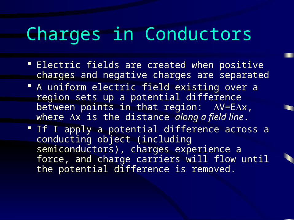
Charges in Conductors
Electric fields are created when positive charges and negative charges are separated
A uniform electric field existing over a region sets up a potential difference between points in that region: V=Ex, where x is the distance along a field line.
If I apply a potential difference across a conducting object (including semiconductors), charges experience a force, and charge carriers will flow until the potential difference is removed.
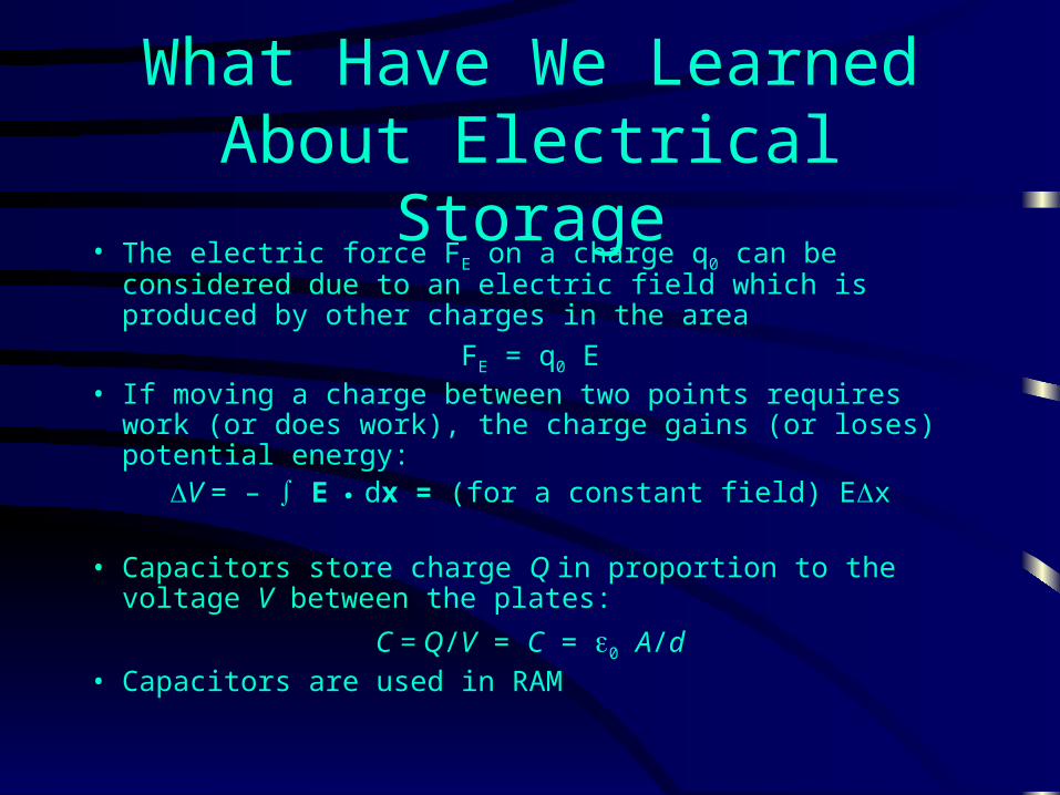
What Have We Learned About Electrical Storage
• The electric force FE on a charge q0 can be considered due to an electric field which is produced by other charges in the area
FE = q0 E• If moving a charge between two points requires work (or does
work), the charge gains (or loses) potential energy:V = – E dx = (for a constant field) Ex
• Capacitors store charge Q in proportion to the voltage V between the plates:
C = Q/V = C = 0 A/d• Capacitors are used in RAM
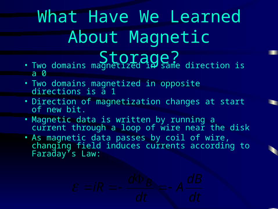
What Have We Learned About Magnetic Storage?
• Two domains magnetized in same direction is a 0• Two domains magnetized in opposite directions is
a 1• Direction of magnetization changes at start of new
bit.• Magnetic data is written by running a current
through a loop of wire near the disk• As magnetic data passes by coil of wire, changing
field induces currents according to Faraday’s Law:
dt
dBA
dt
diR B
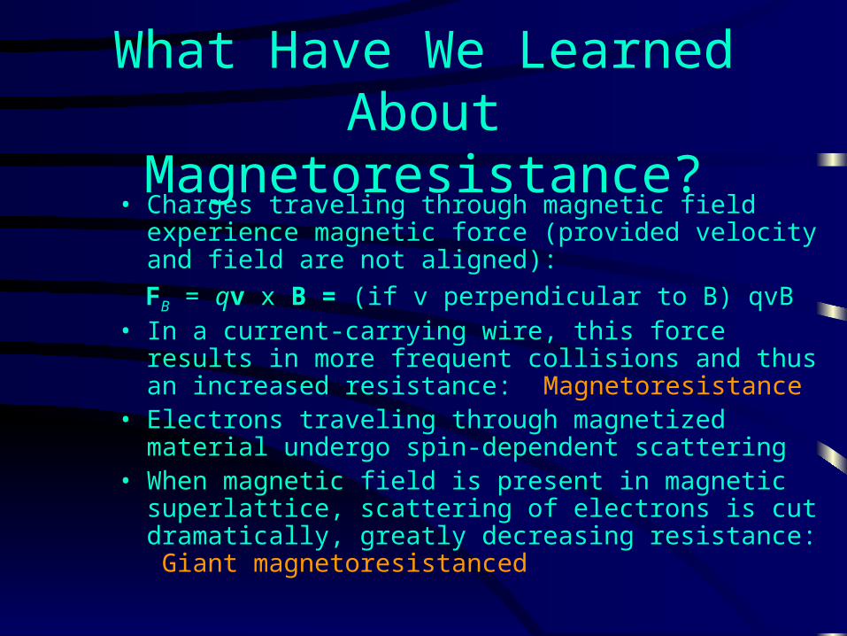
What Have We Learned About Magnetoresistance?
• Charges traveling through magnetic field experience magnetic force (provided velocity and field are not aligned):
FB = qv x B = (if v perpendicular to B) qvB• In a current-carrying wire, this force results in more
frequent collisions and thus an increased resistance: Magnetoresistance
• Electrons traveling through magnetized material undergo spin-dependent scattering
• When magnetic field is present in magnetic superlattice, scattering of electrons is cut dramatically, greatly decreasing resistance: Giant magnetoresistanced
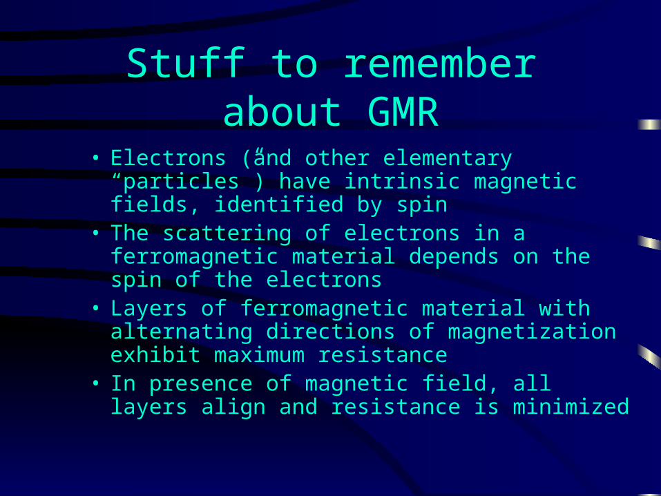
Stuff to remember about GMR
• Electrons (and other elementary “particles”) have intrinsic magnetic fields, identified by spin
• The scattering of electrons in a ferromagnetic material depends on the spin of the electrons
• Layers of ferromagnetic material with alternating directions of magnetization exhibit maximum resistance
• In presence of magnetic field, all layers align and resistance is minimized
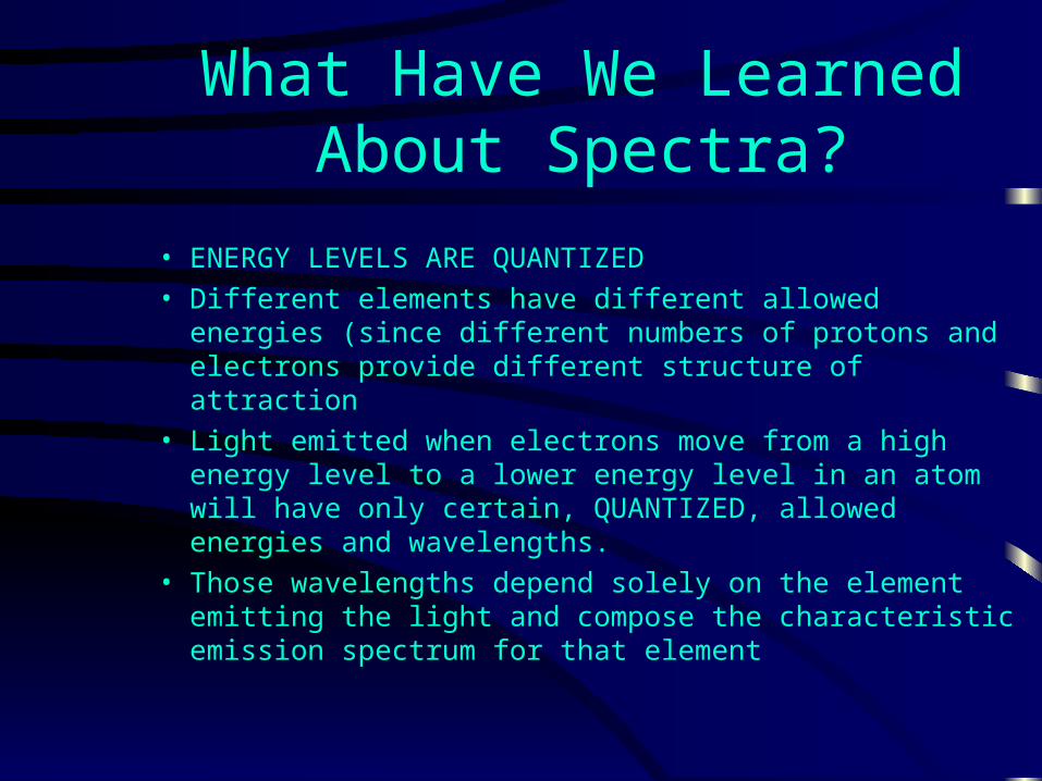
What Have We Learned About Spectra?
• ENERGY LEVELS ARE QUANTIZED
• Different elements have different allowed energies (since different numbers of protons and electrons provide different structure of attraction
• Light emitted when electrons move from a high energy level to a lower energy level in an atom will have only certain, QUANTIZED, allowed energies and wavelengths.
• Those wavelengths depend solely on the element emitting the light and compose the characteristic emission spectrum for that element
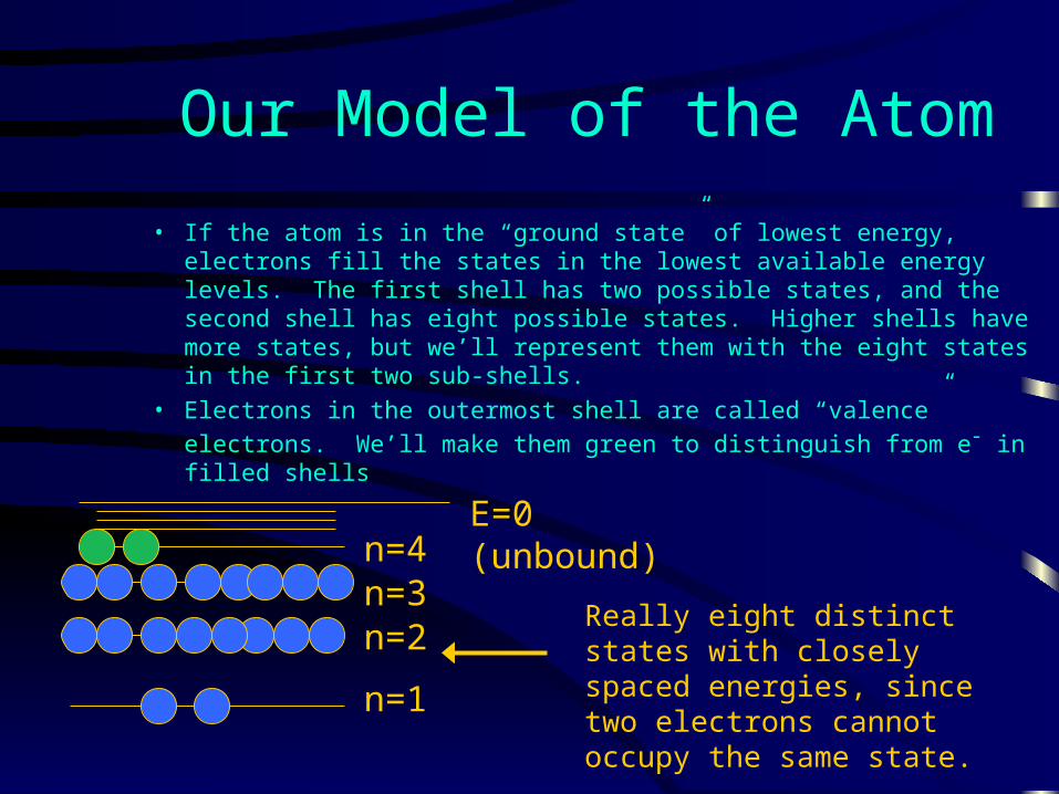
Our Model of the Atom
• If the atom is in the “ground state” of lowest energy, electrons fill the states in the lowest available energy levels. The first shell has two possible states, and the second shell has eight possible states. Higher shells have more states, but we’ll represent them with the eight states in the first two sub-shells.
• Electrons in the outermost shell are called “valence” electrons. We’ll
make them green to distinguish from e- in filled shells
E=0 (unbound)
n=1
n=2n=3n=4
Really eight distinct states with closely spaced energies, since two electrons cannot occupy the same state.

Electrons in Solids• The shifted energies in adjacent atoms combine to create a continuous
“band” of allowed energies for each original energy level; each band, however, has a finite number of states equal to the number in original atoms
• Electrons can move from the locality of one atom to the next only if an energy state is available within the same band
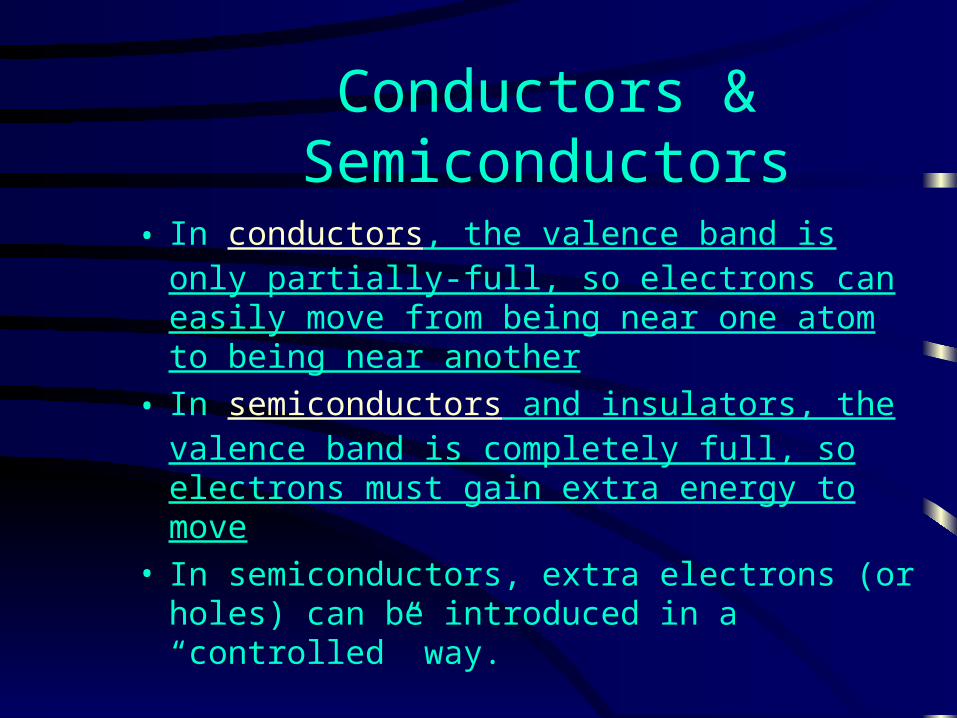
Conductors & Semiconductors
• In conductors, the valence band is only partially-full, so electrons can easily move from being near one atom to being near another
• In semiconductors and insulators, the valence band is completely full, so electrons must gain extra energy to move
• In semiconductors, extra electrons (or holes) can be introduced in a “controlled” way.
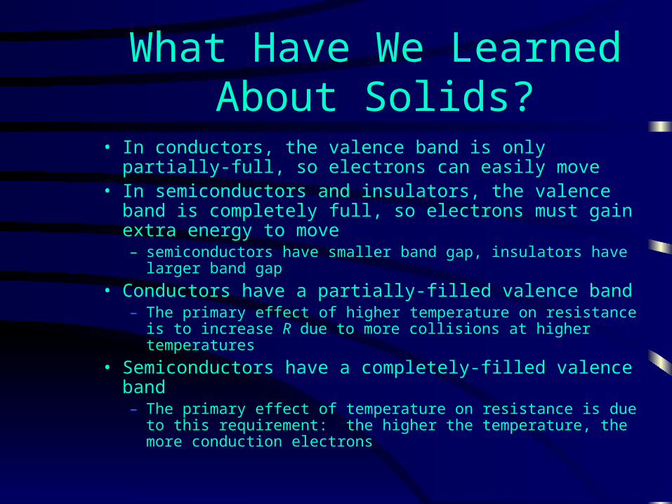
What Have We Learned About Solids?
• In conductors, the valence band is only partially-full, so electrons can easily move
• In semiconductors and insulators, the valence band is completely full, so electrons must gain extra energy to move– semiconductors have smaller band gap, insulators have larger band
gap
• Conductors have a partially-filled valence band– The primary effect of higher temperature on resistance is to increase
R due to more collisions at higher temperatures
• Semiconductors have a completely-filled valence band– The primary effect of temperature on resistance is due to this
requirement: the higher the temperature, the more conduction electrons
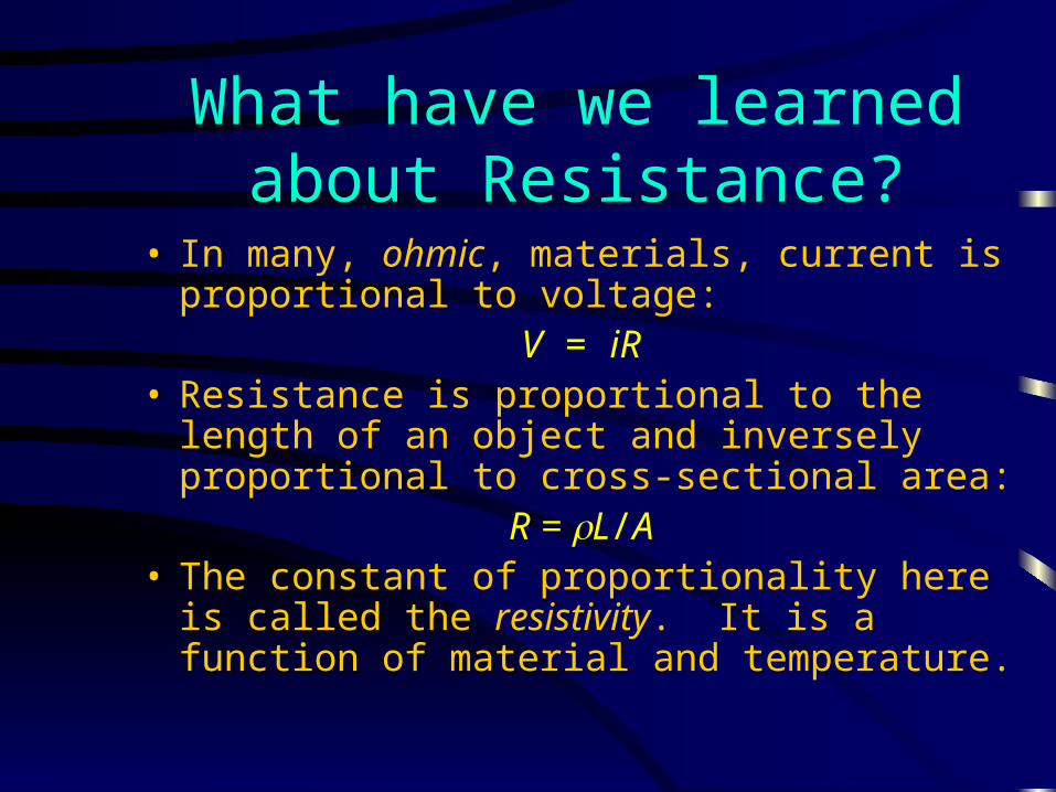
What have we learned about Resistance?
• In many, ohmic, materials, current is proportional to voltage:
V = iR• Resistance is proportional to the length of an
object and inversely proportional to cross-sectional area:
R = L/A• The constant of proportionality here is called the
resistivity. It is a function of material and temperature.
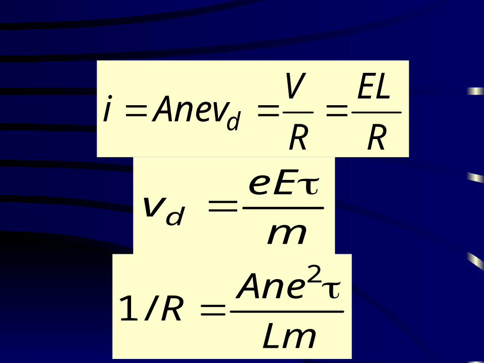
R
EL
R
VAnevi d
m
eEvd
Lm
AneR
2
/1
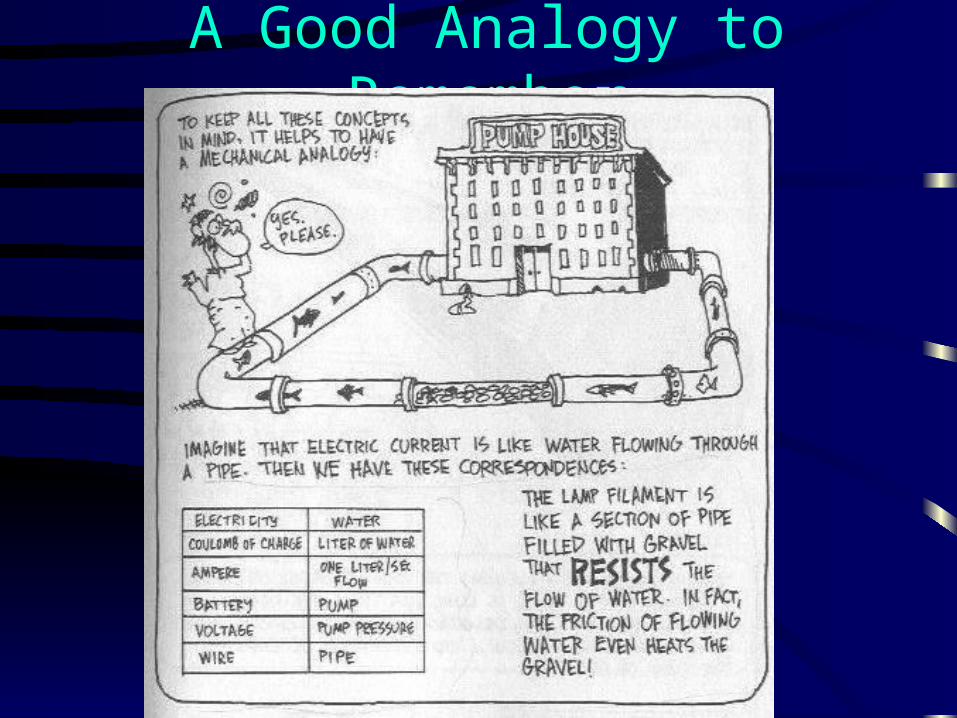
A Good Analogy to Remember
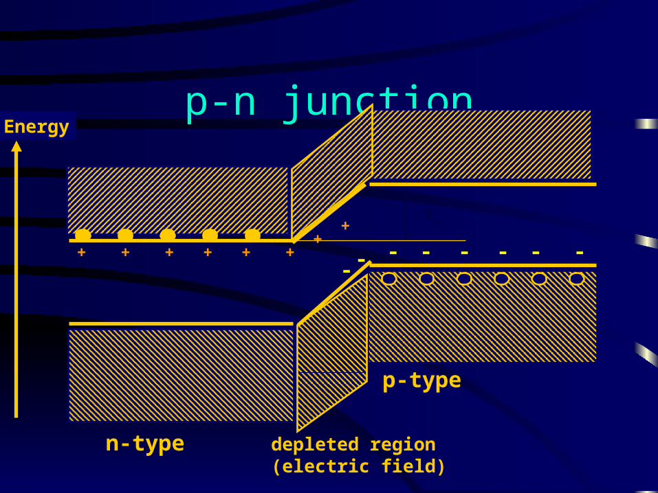
p-n junction
n-type
p-type
Energy
depleted region(electric field)
+ + + + + ++
+
--------
Vo

Wide Bandgap Semiconductors
What is a wide bandgap semiconductor?
Larger energy gap allows higher power and temperature operation and the generation of more energetic (i.e. blue) photons
Traditional wide bandgap semiconductors include AlAs/GaAs, SiC
The III-nitrides (AlN, GaN and InN) have recently become feasible.
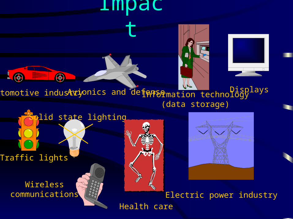
Impact
Automotive industry Avionics and defense
Traffic lights
Solid state lighting
Electric power industry
Health care
Information technology(data storage)
Wirelesscommunications
Displays

Heterojunctions