reviewarticle status and prospects of al -based · pdf filereviewarticle status and prospects...
TRANSCRIPT

REVIEW ARTICLE
Status and prospects of Al2O3-based surface passivation schemesfor silicon solar cells
G. Dingemans and W. M. M. Kesselsa)
Department of Applied Physics, Eindhoven University of Technology, P.O. Box 513, 5600 MB Eindhoven,The Netherlands
(Received 18 February 2012; accepted 25 May 2012; published 6 July 2012)
The reduction in electronic recombination losses by the passivation of silicon surfaces is a critical
enabler for high-efficiency solar cells. In 2006, aluminum oxide (Al2O3) nanolayers synthesized by
atomic layer deposition (ALD) emerged as a novel solution for the passivation of p- and n-type
crystalline Si (c-Si) surfaces. Today, high efficiencies have been realized by the implementation of
ultrathin Al2O3 films in laboratory-type and industrial solar cells. This article reviews and
summarizes recent work concerning Al2O3 thin films in the context of Si photovoltaics. Topics
range from fundamental aspects related to material, interface, and passivation properties to
synthesis methods and the implementation of the films in solar cells. Al2O3 uniquely features a
combination of field-effect passivation by negative fixed charges, a low interface defect density, an
adequate stability during processing, and the ability to use ultrathin films down to a few
nanometers in thickness. Although various methods can be used to synthesize Al2O3, this review
focuses on ALD—a new technology in the field of c-Si photovoltaics. The authors discuss how the
unique features of ALD can be exploited for interface engineering and tailoring the properties of
nanolayer surface passivation schemes while also addressing its compatibility with high-throughput
manufacturing. The recent progress achieved in the field of surface passivation allows for higher
efficiencies of industrial solar cells, which is critical for realizing lower-cost solar electricity in the
near future. VC 2012 American Vacuum Society. [http://dx.doi.org/10.1116/1.4728205]
I. INTRODUCTION
Over 85% of the solar cells currently produced are based
on crystalline silicon wafers. The lion’s share of these indus-
trially manufactured cells have energy conversion efficiencies
of typically g ¼ 16%–18%, while the record of g ¼ 25.0% for
laboratory-type Si solar cells1,2 is already fairly close to the
theoretical maximum of g ¼ �29%.3–8 The efficiency of solar
cells is significantly affected by electronic recombination
losses at the wafer surfaces—primarily through a suboptimal
open-circuit voltage. A reduction in surface recombination is
called surface passivation. At present, only a fraction of indus-
trial solar cells has effective passivation schemes imple-
mented, which explains a significant part of the efficiency gap
between industrial cells and high-efficiency laboratory cells.9
Over the years, various materials and material stacks have
been investigated for surface passivation purposes of the
cell’s front and rear side.10 The suitability of a passivation
scheme depends on doping type and Si resistivity and on
aspects such as the thermal-, UV-, and long-term stability,
the optical properties (i.e., parasitic absorption, refractive
index), and the processing requirements (e.g., surface clean-
ing, available synthesis methods). Silicon nitride (a-SiNx:H)
is an important material in Si photovoltaics as it is used in
virtually all (laboratory and industrial) solar cells as antire-
flective coating. a-SiNx:H also provides (some) surface pas-
sivation and passivation of bulk defects for multicrystalline
Si. Traditionally, thermally grown SiO2 has been used as
effective passivation scheme in high-efficiency laboratory
cells, for instance in the record passivated emitter rear
locally diffused (PERL) cell.1,2 Another widely investigated
material is amorphous Si (a-Si:H). The combination of
intrinsic and doped a-Si:H nanolayers (<10 nm) has been
successfully applied in (commercial) heterojunction solar
cells.11
Aluminum oxide (Al2O3) has recently emerged as an al-
ternative passivation material. Although not outstanding at
that time, the passivation properties of Al2O3 were already
reported in 1989 by Hezel and Jaeger.12 Nonetheless, their
publication was written for posterity. Al2O3 technology
gained momentum only after its reintroduction—this time
synthesized by atomic layer deposition (ALD).13–15 The
level of passivation that was demonstrated by Hoex et al. in
2006 for Al2O3 on lowly doped Si and pþ emitters was at
least as good as obtained by thermally grown SiO2.14,16
Compared to other investigated materials, a distinguishing
property of Al2O3 appeared to be the field-effect passivation
induced by negative fixed charges.14,17
The popularity of Al2O3 can be explained by two im-
portant trends. First, the photovoltaics (PV) industry hasa)Electronic mail: [email protected]
040802-1 J. Vac. Sci. Technol. A 30(4), Jul/Aug 2012 0734-2101/2012/30(4)/040802/27/$30.00 VC 2012 American Vacuum Society 040802-1
Downloaded 10 Jul 2012 to 131.155.113.183. Redistribution subject to AVS license or copyright; see http://avspublications.org/jvsta/about/rights_and_permissions
recently been looking to improve the rear side of
conventional screen-printed p-type Si solar cells by replac-
ing the Al-backsurface field (Al-BSF) by a dielectrically pas-
sivated rear. The latter leads to lower surface recombination
losses, better internal reflection, and reduced wafer bow for
thin wafers. The adoption of a passivated rear side is inevita-
ble concerning the demand for higher efficiencies and the
use of thinner Si wafers. While the availability of (laser)
processes to produce local rear contacts was not a (promi-
nent) bottleneck anymore, the availability of suitable
passivation schemes was. Due to inversion layer shunting,
a-SiNx:H was not a suitable candidate for the p-type Si rear.
Due to reasons of costs, complexity, and a possible adverse
impact of high temperatures on the bulk quality, thermal
oxidation was also not a first choice. Although plasma de-
posited SiOx/SiNx stacks were considered as alternatives,18
the focus shifted to Al2O3 (and Al2O3/SiNx stacks) as a
solution for the p-type Si rear side. Second, for n-type Si so-
lar cells a suitable passivation solution of the pþ emitter was
required. The negative charges of Al2O3 are an ideal match
for the passivation of such emitters. To date, the application
of Al2O3 on pþ emitters and on the p-type Si rear
has resulted in enhanced solar cell efficiencies up to
23.9%.9,19
Along with the introduction of Al2O3 came the introduc-
tion of ALD in the field of Si PV. ALD differs from conven-
tional (plasma-enhanced) chemical vapor deposition
methods by the strict separation of the precursor gases in
two half-cycles during deposition leading to self-limiting
layer-by-layer growth. The hallmark of ALD is precise
thickness control and very uniform and conformal deposition
over large area surfaces. For these reasons, the technique has
recently been adopted for the synthesis of high-k nanolayers
(such as Hf-based oxides) in the semiconductor industry. For
the PV industry, high-throughput spatial and batch ALD
equipment have been designed in the last few years and are
already commercially available.20,21
In this review article, we aim to discuss the progress in
the development and understanding of the properties of
Al2O3-based surface passivation schemes over the last few
years. In doing so, relevant literature will be referenced, but
also some previously unpublished experimental results have
been included. The focus will be on Al2O3 deposited by
atomic layer deposition. The further development, adoption,
and integration of Al2O3-based passivation schemes will rely
on an understanding of the properties underlying the synthe-
sis and key properties of the films. This article aims to con-
tribute to the latter. After a general introduction about the
basics of surface passivation (Sec. II), the synthesis methods
and Al2O3 material properties will be discussed (Sec. III).
Subsequently, atomic layer deposition of Al2O3 will be
addressed in detail in Sec. IV. Section V covers the surface
passivation properties and underlying mechanisms. Section
VI reports on technological aspects that are relevant for the
application of Al2O3-based surface passivation schemes in
(industrial) solar cells. Finally, in Sec. VII, recent progress
on the high-efficiency solar cells featuring Al2O3 films is
reviewed.
II. SURFACE PASSIVATION: BASICSAND APPLICATIONS
A. Surface passivation mechanisms
It is insightful to discuss the rate of surface recombina-
tion, Us (expressed in cm�2 s�1), by its description in the
Shockley–Read-Hall (SRH) formalism.22,23 Us can be
expressed as a function of the interface defect density (Nit,
expressed in cm�2), the hole and electron capture cross sec-
tions (rp/n), and the hole and electron densities at the surface
(ps and ns, respectively),24–27
Us ¼ðnsps � n2
i ÞvthNit
ns þ n1
rpþ ps þ p1
rn
¼ nsps � n2i
ns þ n1
Spþ ps þ p1
Sn
� nspsns
Spþ ps
Sn
:
(1a)
The parameter vth represents the thermal velocity of the elec-
trons, n1 and p1 statistical factors, ni the intrinsic carrier con-
centration, and Sn/p ¼ rn/pvthNit. For sake of the discussion
here, the energy dependence of the parameters (rn/p, n1, p1,
and Nit) is neglected by assuming a single defect at midgap.
In the latter case, and for relevant illumination and doping
levels, n1, p1 and ni � ns and ps, and can therefore be
neglected in Eq. (1a). In reality, the energy levels associated
with surface defects (e.g., dangling bonds) are distributed
throughout the bandgap due to slight variations in structure
and bond angle. Therefore, formally, Us should be expressed
by the extended SRH formalism with an integral over
the bandgap energies while replacing Nit by Dit (in units of
eV�1 cm�2).24,26 As follows from the simple expression in
Eq. (1a), the driving force in surface recombination proc-
esses is the term (nsps – n2i ), which describes the deviation of
the system from thermal equilibrium under illumination.
Equation (1a) shows that Us can be decreased by a reduction
in Nit (or Dit), which is referred to as chemical passivation.
In a recombination event both electrons and holes are
involved. It is notable that the highest recombination rate is
achieved when ps/ns � rn/rp,27 with the ratio of the cross
sections being dependent on the details of the passivation
scheme. Consequently, another way to reduce the recombi-
nation is by a significant reduction in the density of one type
of charge carrier at the surface by an electric field. This is
called field-effect passivation.27,28 We note that, apart from
the SRH model, also the amphoteric nature of dangling
bonds can be used to describe chemical and field-effect pas-
sivation, as reported by Olibet et al.29
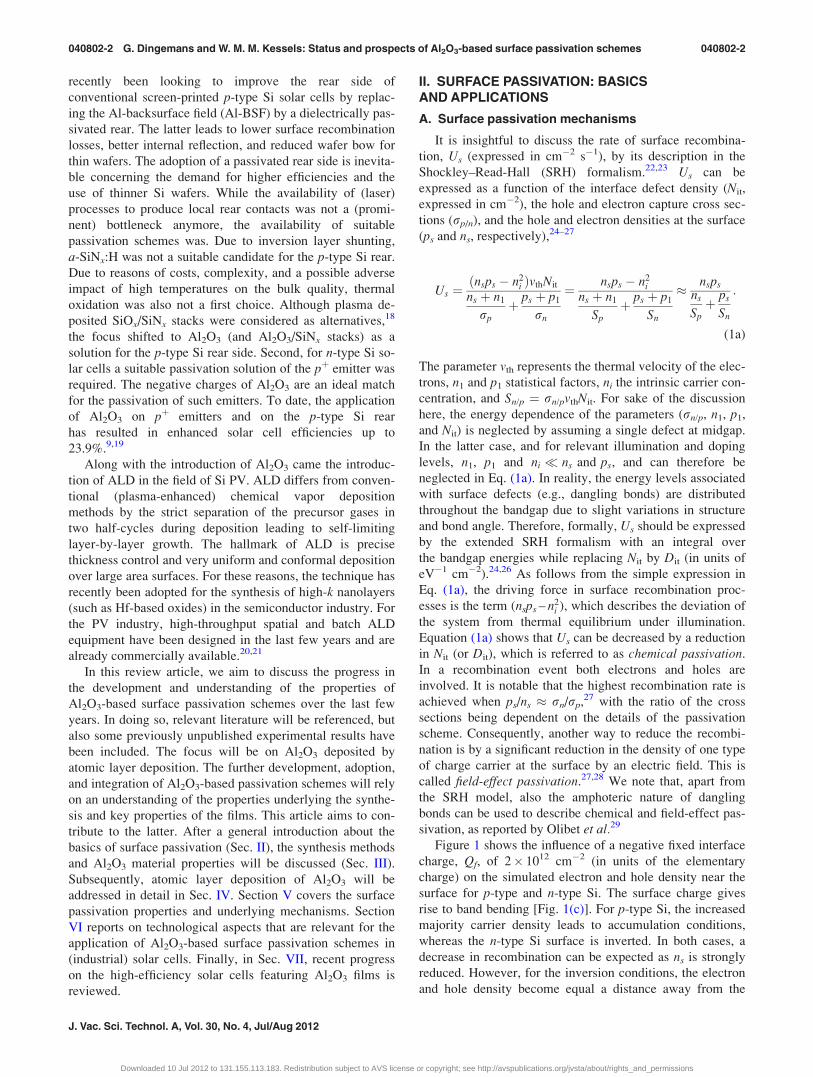
Figure 1 shows the influence of a negative fixed interface
charge, Qf, of 2� 1012 cm�2 (in units of the elementary
charge) on the simulated electron and hole density near the
surface for p-type and n-type Si. The surface charge gives
rise to band bending [Fig. 1(c)]. For p-type Si, the increased
majority carrier density leads to accumulation conditions,
whereas the n-type Si surface is inverted. In both cases, a
decrease in recombination can be expected as ns is strongly
reduced. However, for the inversion conditions, the electron
and hole density become equal a distance away from the
040802-2 G. Dingemans and W. M. M. Kessels: Status and prospects of Al2O3-based surface passivation schemes 040802-2
J. Vac. Sci. Technol. A, Vol. 30, No. 4, Jul/Aug 2012
Downloaded 10 Jul 2012 to 131.155.113.183. Redistribution subject to AVS license or copyright; see http://avspublications.org/jvsta/about/rights_and_permissions
interface. This phenomenon can be expected to enhance
recombination in the subsurface when bulk defects are
present.
A measure that reflects the level of surface passivation is
the surface recombination velocity S:
S � Us
Dn; (1b)
with Dn the injection level. It is possible to deduce an effec-
tive surface recombination velocity, Seff, from the effective
lifetime of the minority carriers in the Si substrate, seff. The
effective lifetime is often measured by the photoconductance
decay technique and is controlled by bulk- and surface
recombination processes,30–33
1
seff
¼ 1
sSRH
þ 1
sAuger
þ 1
srad
� �bulk
þ 1
ssurf
: (2a)
Equation (2a) illustrates that both intrinsic (Auger and radia-
tive recombination) and extrinsic recombination processes
determine bulk recombination. Extrinsic recombination via
bulk defects is also known as SRH recombination. Impur-
ities, such as Fe,34 lattice faults, and dangling bonds at grain
boundaries (multicrystalline Si) can all represent bulk defect
states. In addition, boron–oxygen complexes, formed during
illumination, can be prominent recombination centers, espe-
cially for monocrystalline p-type Si grown by the Czochralski
method (Cz-Si).35–38 These defects limit the maximum bulk
lifetime. On the other hand, for high quality float-zone (FZ)
Si, Auger recombination and, to a lesser extent, radiative
recombination are generally more important processes than
recombination through bulk defects, especially at high injec-
tion levels.
For a symmetrically passivated wafer with sufficiently
low Seff values, Eq. (2a) can be expressed as
1
seff
¼ 1
sbulk
þ 2Seff
W; (2b)
with W the wafer thickness. The relative error in Seff is typi-
cally below 4% for S values <250 cm/s.24,30 For poorly pas-
sivated surfaces, a term accounting for the diffusion of
minority carriers toward the surface is required to improve
the accuracy as described by
1
seff
¼ 1
sbulk
þ W
2Seff
þ 1
Dn
W
p
� �2 !�1
; (2c)
with Dn the diffusion coefficient (with a typical value of
30 cm2/s).24 To calculate the exact value for Seff by Eq. (2b),
the bulk lifetime—which is generally not known—is
required as an input parameter. Some authors use the general
parameterization of the Auger recombination by Kerr and
Cuevas for wafers with various resistivities to obtain a mea-
sure for the bulk lifetime.39 However, it should be noted that
these values represent an approximation (derived under the
assumption that Seff was 0 cm/s). In fact, Benick et al. have
reported seff values above the “intrinsic Auger limit” as
derived by Kerr and Cuevas, suggesting that the intrinsic
lifetime can be higher in reality.40 In addition, sbulk may
vary significantly from wafer to wafer due to the presence of
SRH recombination. Alternatively, an upper level of Seff can
be calculated by assuming that recombination only occurs at
the wafer surfaces (i.e., sbulk ¼1),
Seff;max ¼ Seff <W
2seff
: (2d)
Seff,max is a good approximation for the actual value of Seff
(for injection levels for which Auger recombination is not
dominant) when the passivation properties are evaluated on
Si wafers with high bulk lifetimes (> 1 ms). On the other
hand, for an excellent surface passivation quality, with the
surface recombination approaching 0 cm/s, the effective life-
time becomes dominated by intrinsic recombination proc-
esses which will limit the minimal value of Seff that can be
experimentally determined.
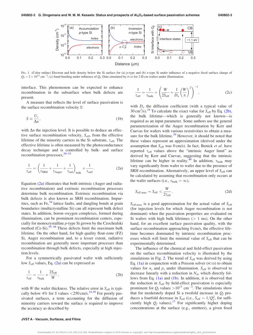
The influence of the chemical and field-effect passivation
on the surface recombination velocity is illustrated by the
simulations in Fig. 2. The trend of Seff was derived by using
Eq. (1a) in conjunction with a Poisson solver (PC1D) to obtain
values for ns and ps under illumination. Seff is observed to
decrease linearly with a reduction in Nit, which directly fol-
lows from Eq. (1a) and (1b). In addition, it is observed that
the reduction in Seff by field-effect passivation is especially
prominent for Qf values >1011 cm�2. The simulations show
that for moderately doped Si a twofold increase in Qf pro-
duces a fourfold decrease in Seff (i.e., Seff � 1=Q2f , for suffi-
ciently high Qf values).17 For significantly higher doping
concentrations at the surface (e.g., emitters), a given fixed
0.0 0.1 0.2 0.3
Distance (μm)
holes
electrons
n = p
Si i
nter
face
with
Qf
Den
sity
(cm
-3)
0.0 0.1 0.2 0.31013
1015
1017
1019
electrons
Inversionn-type Si
Accumulationp-type Si
holes
0.0 0.1 0.2 0.3
(c)(b)
VB
Interface states
CB
~1.1 eV
(a)
FIG. 1. (Color online) Electron and hole density below the Si surface for (a) p-type and (b) n-type Si under influence of a negative fixed surface charge of
Qf ¼ 2� 1012 cm�2; (c) band bending under influence of Qf. Data simulated by PC1D for 2 X cm wafers under illumination.
040802-3 G. Dingemans and W. M. M. Kessels: Status and prospects of Al2O3-based surface passivation schemes 040802-3
JVST A - Vacuum, Surfaces, and Films
Downloaded 10 Jul 2012 to 131.155.113.183. Redistribution subject to AVS license or copyright; see http://avspublications.org/jvsta/about/rights_and_permissions
charge density has a relatively smaller influence on band
bending and the charge carrier densities (not shown). Conse-
quently, the influence of the (additional) field-effect passiva-
tion induced by the passivation scheme becomes smaller for
higher doping densities.
Figure 2 also shows that the trend between Seff and Qf
changes significantly when the value of rn/rp is increased
from 1 to 102. In the latter case, a maximum appears in Seff
at Qf ¼ �2� 1011cm�2, which coincides with the condition
for maximum recombination (ps/ns ¼ rn/rp ¼ 102). In addi-
tion, higher Qf values >4� 1011 cm�2 appear to be required
to activate the field-effect passivation. It is notable that, for
the case of Al2O3, a value of rn=rp � 1 is probably more re-
alistic than rn=rp ¼ 1. As will be discussed later, the Si/
Al2O3 interface is essentially “Si/SiO2”-like.41 The value of
rn/rp ¼ �102 reported for thermally grown SiO2 interfaces
may therefore be a better assumption for the Si/Al2O3
interface.28,42
The experimentally accessible parameter, Seff,max, is also
given in Fig. 2. Seff,max was derived by combining Eqs. (2b)
and (2d) and substituting a bulk lifetime of 10 ms. Figure 2
shows that for a very high level of surface passivation,
Seff,max becomes limited by the bulk lifetime. In that case,
Seff,max does not reflect the actual (extremely low) Seff values
anymore. This implies, for instance, that significant varia-
tions of Qf> 1� 1012 cm�2 are not expected to lead to dras-
tic changes in the measured Seff,max values.
B. Surface passivation materials
The most important surface passivation materials used in
photovoltaics include SiO2, a-SiNx:H, and a-Si:H.
Considering the recent progress, Al2O3 can now be added to
this list.
1. SiO2
The high quality interface between thermally grown SiO2
and Si contributed significantly to the dominance of Si in the
microelectronics industry43 and is also responsible for high
solar cell efficiencies.44,45 Thermal SiO2 leads to very low
surface recombination velocities (Seff< 10 cm/s) after form-
ing gas annealing or alnealing (using a sacrificial Al
layer).45–49 The hydrogen that is introduced during the
annealing process passivates the electronically active defects
such as the prominent Pb-type defect which constitutes an Si
dangling bond ( Si). This leads to typical defect densities
of the order of 1010 cm�2 eV�1.46,50 Field-effect passivation
is not prominent with comparatively low values of Qf in the
range of 1010–1011 cm�2. Hence, an important benefit of
thermal SiO2 is the high level of chemical passivation that
can be achieved for both n- and p-type Si surfaces over a
wide range of relevant doping levels. Moreover, it can be
used to engineer diffusion profiles. Thermal oxidation can be
carried out in H2O-vapor (T � 850–900 C) or O2 atmos-
phere (T � 950–1000 C).44,45,49 The growth rate for the for-
mer “wet” thermal process is significantly higher than for
the “dry” process. Various other methods have been
explored for developing SiO2 surface passivation films at
low temperatures. Low-temperature processing can be tech-
nologically interesting as it opens up the possibility for using
materials that are less thermally stable and avoids the risk of
bulk lifetime degradation. The most widely investigated
low-temperature method is plasma-enhanced chemical vapor
deposition (PECVD), which allows for high-throughput
processing.18,51,52 Another option for the synthesis of SiOx is
a chemical oxidation of the Si surface, for example using
HNO3.53,54 A drawback of this method is that it can only
produce SiOx with a thickness of a few nanometers. In gen-
eral, the level of passivation induced by single layer SiO2
synthesized at low temperatures is seriously lower than
obtained by thermal oxidation processes. However, these
properties can be improved drastically by the application of
a-SiNx:H or Al2O3 capping layers (see Sec. VI B).
2. a-SiNx:H
The working horse thin film dielectric in c-Si photovol-
taics is a-SiNx:H (for brevity, SiNx) synthesized by
PECVD.55–61 Owing to the fact that the optical properties of
the material can be varied in a wide range, SiNx is the stand-
ard for antireflection coatings in solar cells. Figure 3 shows
the material composition in terms of the atomic H, Si, and
N density as a function of the refractive index. Films with
comparatively high nitrogen content exhibit refractive indi-
ces of approximately 2, which results in optimal antireflec-
tion properties when applied on the front side of a solar cell.
The films also contain a relatively large amount of hydrogen
of �10–15 at. %. The hydrogen released during firing plays
an important role in the bulk passivation of multicrystalline
Si.61–63 Depending on film composition, the films provide a
reasonable to high level of passivation. Optimal surface pas-
sivation is generally achieved for relatively Si-rich films.
However, the nitrogen-rich films exhibit a superior thermal
109 1010 1011 1012 101310-1
100
101
102
103
Nit = 1011 cm-2
Nit = 1010 cm-2
σn/σp=1
Seff,max
Nit = 1011 cm-2, σn/σp=1
Nit = 1012 cm-2, σn/σp=1S
eff &
Sef
f,max
(cm
/s)
Qf (cm-2)
Seff,max limited by bulk
Seff
σn/σp=102
FIG. 2. (Color online) Simulated Seff and Seff,max values using Eq. (1a) and
(1b) and the relation between negative Qf and ps and ns using PC1D. The val-
ues used for the defect cross sections (rn ¼ rp ¼ 10�16 cm�2) are somewhat
arbitrary but of a typical order of magnitude. Note that these values affect
the scaling between Seff and Nit (vertical axis) and not the qualitative picture.
For ratio of rn/rp ¼ 102, values of rn ¼ 10�15 cm�2; rp ¼ 10�17 cm�2 were
used. Other values included a bulk resistivity of 2 X cm p-type Si (doping of
7.2� 1015 cm�3) and an injection level of Dn ¼ 5� 1014 cm�3. To calculate
Seff,max, a value of sbulk ¼ 10 ms was used. The simulation is an approxima-
tion to illustrate general trends.
040802-4 G. Dingemans and W. M. M. Kessels: Status and prospects of Al2O3-based surface passivation schemes 040802-4
J. Vac. Sci. Technol. A, Vol. 30, No. 4, Jul/Aug 2012
Downloaded 10 Jul 2012 to 131.155.113.183. Redistribution subject to AVS license or copyright; see http://avspublications.org/jvsta/about/rights_and_permissions

and chemical stability and can be useful as a capping layer
on Al2O3. The passivation mechanisms of the a-SiNx:H films
strongly depend on the nitrogen content. When the nitrogen
content is relatively low, the films exhibit amorphous Si-like
properties. In this case, the high level of passivation is
mainly governed by chemical passivation. On the other hand,
for high [N], the films induce a significant amount of field-
effect passivation with fixed charge densities of the order of
1012 cm�2, as shown in the following. This is related to the
so-called K-center (an Si atom backbonded with three N
atoms) that can be charged positively [see Fig. 3 (inset)].64–67
A significant positive charge density leads to inversion con-
ditions for p-type Si surfaces. Strong inversion can give rise
to transport properties parallel to the interface. a-SiNx
applied on the rear side of a p-type Si solar cell can therefore
compromise solar cell performance by the so-called parasitic
or inversion layer shunting effect.67 SiO2/SiNx stacks are
expected to reduce or nullify this detrimental effect.68,69
3. a-Si:H
Hydrogenated amorphous Si (a-Si:H) is a semiconductor;
in contrast to the dielectrics discussed so far. a-Si:H leads
to excellent passivation properties with Seff as low as
2 cm/s.70–75 The growth related material properties of
PECVD a-Si:H have been studied in depth for applications
such as thin film Si solar cells.76–80 This knowledge is also
useful for the optimization and understanding of the a-Si:H
properties for crystalline Si technology. In particular, hetero-
junction solar cells have attracted considerable attention in
recent years.11,81–83 For such cells, high-temperature dopant
diffusion processes are replaced by the deposition of doped
a-Si:H films at low temperature. The surface passivation and
unique contacting approach contribute to high open-circuit
voltages (>700 mV). Efficiencies of 23.7% have been
achieved using industrial processes.84 Limitations of the
application of a-Si:H surface passivation films are parasitic
absorption effects and the lack of thermal stability during
high-temperature processes (such as contact firing). The lat-
ter is an impediment to the use of a-Si:H in standard screen-
printed solar cells.
Significant differences exist between the level of chemical
and field-effect passivation afforded by the various passiva-
tion schemes. Thermal SiO2 and intrinsic a-Si:H do not pro-
vide a high level of field-effect passivation, whereas this
mechanism is quite significant for N-rich SiNx and Al2O3. To
illustrate the differences in the passivation mechanisms of the
materials, corona charging experiments are insightful. In
Fig. 4, Seff,max is plotted as a function of the corona charge
density, ranging from negative to positive, deposited on ALD
Al2O3, N-rich SiNx and SiOx films synthesized by PECVD.
The maximum in Seff,max is a measure for the chemical passi-
vation because at this point the effect of intrinsic charge in the
passivation scheme is nullified by the deposited corona
charges. It is observed that the chemical passivation induced
by Al2O3 is better than obtained by the SiNx or PECVD SiOx
films. In addition, Fig. 4 illustrates that the SiOx and SiNx
films exhibit a positive fixed charge density, whereas Al2O3
leads to a significantly higher and negative Qf.
C. Surface passivation in high-efficiency solar cells
From the previous discussion, the question arises how the
solar cell efficiency is affected by the implementation of a
surface passivation scheme. Here, we consider a conven-
tional p-type Si solar cell as an example to illustrate the
effect of rear surface passivation. By using an Al2O3 film as
dielectric in combination with local contacts [PERC-type
cell (passivated emitter and rear cell)], the solar cell effi-
ciency can be significantly higher than obtained with a full
Al-BSF. This is related to (1) lower Seff values and (2) the
enhanced absorption in photon energy range of 1–1.2 lm by
an enhanced reflection from the solar cell’s rear side. For the
latter, a thickness of the passivation scheme of approxi-
mately 100–150 nm is beneficial.
The optical properties for a PERC cell with Al2O3 on
the rear surface were simulated85 and used as an input for
the PC1D program to simulate solar cell performance. The
enhanced photon absorption for the PERC solar cell relative
-6 -4 -2 0 2 4 6 8 100
100
200
300
400
500
Qf= −5x1012 cm-2
Al2O3
Sef
f,max
(cm
/s)
Corona charge density (1012 cm-2)
a-SiNx:HQf= +3x1012 cm-2
PECVD SiOx
Q = +1x1012 cm-2f
FIG. 4. (Color online) Seff,max vs deposited corona charge density for
a-SiNx:H (�80 nm, after firing) and PECVD SiOx (�50 nm) and Al2O3 films
(�30 nm) after annealing at 400 C in H2/N2 and N2, respectively.
1.8 2.0 2.2 2.4 2.6 2.80
20
40
60
80Si
NSiSi
Si
NSiN
Si
NNN
Si,
N, H
(at %
)
Refractive index
[Si]
[N]
[H]
FIG. 3. (Color online) Composition of a-SiNx:H films in terms of H, Si, and
N density plotted over the resulting refractive index. The films were depos-
ited in a Roth & Rau MW-PECVD reactor. The atomic densities were
obtained by Rutherford backscattering spectroscopy and elastic recoil detec-
tion. The inset shows some possible bonding configurations of Si (with dan-
gling bonds) where N3:Si– represents the amphoteric K-center, which is
typically positively charged for a-SiNx:H films on Si substrates.
040802-5 G. Dingemans and W. M. M. Kessels: Status and prospects of Al2O3-based surface passivation schemes 040802-5
JVST A - Vacuum, Surfaces, and Films
Downloaded 10 Jul 2012 to 131.155.113.183. Redistribution subject to AVS license or copyright; see http://avspublications.org/jvsta/about/rights_and_permissions
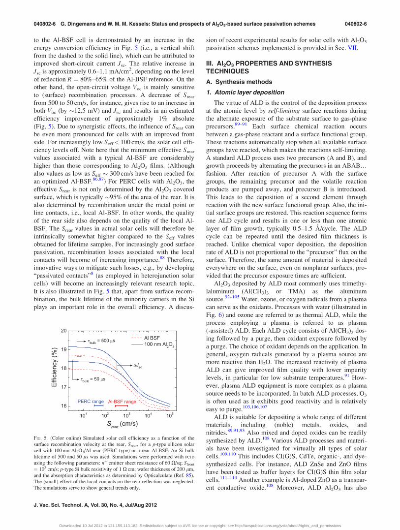
to the Al-BSF cell is demonstrated by an increase in the
energy conversion efficiency in Fig. 5 (i.e., a vertical shift
from the dashed to the solid line), which can be attributed to
improved short-circuit current Jsc. The relative increase in
Jsc is approximately 0.6–1.1 mA/cm2, depending on the level
of reflection R ¼ 80%–65% of the Al-BSF reference. On the
other hand, the open-circuit voltage Voc is mainly sensitive
to (surface) recombination processes. A decrease of Srear
from 500 to 50 cm/s, for instance, gives rise to an increase in
both Voc (by �12.5 mV) and Jsc and results in an estimated
efficiency improvement of approximately 1% absolute
(Fig. 5). Due to synergistic effects, the influence of Srear can
be even more pronounced for cells with an improved front
side. For increasingly low Seff< 100 cm/s, the solar cell effi-
ciency levels off. Note here that the minimum effective Srear
values associated with a typical Al-BSF are considerably
higher than those corresponding to Al2O3 films. (Although
also values as low as Seff � 300 cm/s have been reached for
an optimized Al-BSF.86,87) For PERC cells with Al2O3, the
effective Srear is not only determined by the Al2O3 covered
surface, which is typically �95% of the area of the rear. It is
also determined by recombination under the metal point or
line contacts, i.e., local Al-BSF. In other words, the quality
of the rear side also depends on the quality of the local Al-
BSF. The Srear values in actual solar cells will therefore be
intrinsically somewhat higher compared to the Seff values
obtained for lifetime samples. For increasingly good surface
passivation, recombination losses associated with the local
contacts will become of increasing importance.88 Therefore,
innovative ways to mitigate such losses, e.g., by developing
“passivated contacts”8 (as employed in heterojunction solar
cells) will become an increasingly relevant research topic.
It is also illustrated in Fig. 5 that, apart from surface recom-
bination, the bulk lifetime of the minority carriers in the Si
plays an important role in the overall efficiency. A discus-
sion of recent experimental results for solar cells with Al2O3
passivation schemes implemented is provided in Sec. VII.
III. Al2O3 PROPERTIES AND SYNTHESISTECHNIQUES
A. Synthesis methods
1. Atomic layer deposition
The virtue of ALD is the control of the deposition process
at the atomic level by self-limiting surface reactions during
the alternate exposure of the substrate surface to gas-phase
precursors.89–91 Each surface chemical reaction occurs
between a gas-phase reactant and a surface functional group.
These reactions automatically stop when all available surface
groups have reacted, which makes the reactions self-limiting.
A standard ALD process uses two precursors (A and B), and
growth proceeds by alternating the precursors in an ABAB…
fashion. After reaction of precursor A with the surface
groups, the remaining precursor and the volatile reaction
products are pumped away, and precursor B is introduced.
This leads to the deposition of a second element through
reaction with the new surface functional group. Also, the ini-
tial surface groups are restored. This reaction sequence forms
one ALD cycle and results in one or less than one atomic
layer of film growth, typically 0.5–1.5 A/cycle. The ALD
cycle can be repeated until the desired film thickness is
reached. Unlike chemical vapor deposition, the deposition
rate of ALD is not proportional to the “precursor” flux on the
surface. Therefore, the same amount of material is deposited
everywhere on the surface, even on nonplanar surfaces, pro-
vided that the precursor exposure times are sufficient.
Al2O3 deposited by ALD most commonly uses trimethy-
laluminum (Al(CH3)3 or TMA) as the aluminum
source.92–105 Water, ozone, or oxygen radicals from a plasma
can serve as the oxidants. Processes with water (illustrated in
Fig. 6) and ozone are referred to as thermal ALD, while the
process employing a plasma is referred to as plasma
(-assisted) ALD. Each ALD cycle consists of Al(CH3)3 dos-
ing followed by a purge, then oxidant exposure followed by
a purge. The choice of oxidant depends on the application. In
general, oxygen radicals generated by a plasma source are
more reactive than H2O. The increased reactivity of plasma
ALD can give improved film quality with lower impurity
levels, in particular for low substrate temperatures.91 How-
ever, plasma ALD equipment is more complex as a plasma
source needs to be incorporated. In batch ALD processes, O3
is often used as it exhibits good reactivity and is relatively
easy to purge.103,106,107
ALD is suitable for depositing a whole range of different
materials, including (noble) metals, oxides, and
nitrides.89,91,93 Also mixed and doped oxides can be readily
synthesized by ALD.108 Various ALD processes and materi-
als have been investigated for virtually all types of solar
cells.109,110 This includes CI(G)S, CdTe, organic-, and dye-
synthesized cells. For instance, ALD ZnSe and ZnO films
have been tested as buffer layers for CI(G)S thin film solar
cells.111–114 Another example is Al-doped ZnO as a transpar-
ent conductive oxide.108 Moreover, ALD Al2O3 has also
FIG. 5. (Color online) Simulated solar cell efficiency as a function of the
surface recombination velocity at the rear, Srear, for a p-type silicon solar
cell with 100 nm Al2O3/Al rear (PERC-type) or a rear Al-BSF. An Si bulk
lifetime of 500 and 50 ls was used. Simulations were performed with PC1D
using the following parameters: nþ emitter sheet resistance of 60 X/sq; Sfront
¼ 105 cm/s; p-type Si bulk resistivity of 1 X cm; wafer thickness of 200 lm,
and the absorption characteristics as determined by Opticalculate (Ref. 85).
The (small) effect of the local contacts on the rear reflection was neglected.
The simulations serve to show general trends only.
040802-6 G. Dingemans and W. M. M. Kessels: Status and prospects of Al2O3-based surface passivation schemes 040802-6
J. Vac. Sci. Technol. A, Vol. 30, No. 4, Jul/Aug 2012
Downloaded 10 Jul 2012 to 131.155.113.183. Redistribution subject to AVS license or copyright; see http://avspublications.org/jvsta/about/rights_and_permissions

been used; for example, as encapsulation layer in CI(G)S
and organic cells.115–118
Benefits of ALD over PECVD and PVD are the excellent
uniformity that can be achieved on large substrates, the rela-
tively low substrate temperatures used in the process (tem-
perature window typically 100–350 C), and the fact that
ALD can readily produce multilayer structures. On the other
hand, due to the purge steps, the ALD cycle times are typi-
cally of the order of a few seconds (single-wafer reactor),
which leads to low deposition rates for temporal ALD. How-
ever, the throughput can be significantly enhanced using
ALD batch reactors or a novel approach based on the spatial
separation of the ALD precursors. These options for high-
volume manufacturing are discussed in detail in Sec. VI C.
2. PECVD
Plasma-enhanced chemical vapor deposition is not a tradi-
tional synthesis method for Al2O3 and the amount of techno-
logically relevant literature available on this topic is limited.
Nevertheless, before Al2O3 became of interest for solar cell
applications, some PECVD processes were reported using Al
precursors such as Al(CH3)3 and AlCl3.119–121 In the last few
years, additional PECVD processes have been developed with
the incentive to mitigate the drawbacks of temporal ALD.
Miyajima et al. were the first to report on PECVD Al2O3 for
surface passivation applications.122,123 They used a capaci-
tively coupled plasma in combination with Al(CH3)3, H2, and
CO2 process gasses. Furthermore, a PECVD process was
developed in an industrial inline reactor that is already widely
used for a-SiNx:H deposition (Roth & Rau).124 The plasma is
created via a linear antenna by 2.45 GHz microwave pulses.
N2O, Al(CH3)3, and argon were used as process gasses. Depo-
sition rates of 100 nm/min could be achieved. Roth &
Rau now offers a tool that enables the deposition of Al2O3
and a-SiNx:H without vacuum break. In addition to the contin-
uous flow processes, an alternative PECVD process has been
reported in which the Al(CH3)3 precursor was pulsed.98,125
This pulsed process leads to additional control over the mate-
rial properties. Collectively, the various reports have shown
that for optimized PECVD processes the passivation quality
of the deposited aluminum oxide films can be quite compara-
ble to that achieved by ALD.
3. Other synthesis methods
In the first report on Al2O3 for surface passivation, atmos-
pheric pressure chemical vapor deposition (APCVD) of
aluminum-triisopropoxide was used.12 Very recently, good
results were reported using a large-scale deposition tool
based on the APCVD method.126 Physical vapor deposition,
i.e., sputtering, has also been applied for the synthesis of
Al2O3 passivation layers. RF magnetron sputtering of an alu-
minum target in an O2/Ar mixture led to deposition rates of
�4 nm/min in a laboratory system.127 Although only prelim-
inary data are available, sputtering appears to produce Al2O3
with a lower level of passivation compared to ALD or
PECVD.
B. Material and interface properties of Al2O3 on Si
The material properties of amorphous Al2O3 vary with
deposition method.98 A prominent factor influencing the
Al2O3 composition is the incorporation of other elements
than O and Al, such as carbon and most notably hydrogen.
For ALD processes, the Al2O3 properties and the hydrogen
content are primarily controlled by the substrate temperature
during deposition Tdep.97,98 Fourier-transform infrared
absorption (FTIR) measurements have indicated that hydro-
gen is incorporated as OH-groups, and that also some CHx
may be present.128 In addition, the presence of carbonates
was observed for Al2O3 films deposited by plasma ALD.
Both the hydrogen and carbon content were observed to
decrease with increasing deposition temperature.
Table I lists the important material properties of ALD
Al2O3. For the relevant range of Tdep ¼ 150–250 C, both
thermal and plasma ALD Al2O3 exhibited a comparable mass
density and refractive index. However, the hydrogen content
for thermal ALD Al2O3 (�3.6 at. %) was higher than for
plasma ALD (�2.7 at. %) at Tdep ¼ 200 C. We verified with
Rutherford backscattering spectroscopy (RBS) and x-ray pho-
toelectron spectroscopy (XPS) that the carbon content in the
films deposited at a temperature of �200 C was negligible
with [C]< 1 at. %. In Fig. 7 data are shown for the refractive
index, n, and extinction coefficient, k, as determined for
plasma ALD Al2O3 films from spectroscopic ellipsometry
measurements. Annealing at 400 C did not change the optical
FIG. 6. (Color online) Schematic of ALD cycle comprising two precursor dosing steps and two purge steps.
040802-7 G. Dingemans and W. M. M. Kessels: Status and prospects of Al2O3-based surface passivation schemes 040802-7
JVST A - Vacuum, Surfaces, and Films
Downloaded 10 Jul 2012 to 131.155.113.183. Redistribution subject to AVS license or copyright; see http://avspublications.org/jvsta/about/rights_and_permissions
properties of the film significantly and thermal ALD with
H2O gave similar results. From the dielectric function e2, an
optical bandgap of Eopt ¼ 6.4 6 0.1 eV was determined for
both the as-deposited and annealed films. This experimentally
determined value for (amorphous) Al2O3 films is lower than
the value of �8.8 eV representative for crystalline Al2O3. The
Al2O3 films crystallize at temperatures above �850 C.129,130
Given the optical bandgap, parasitic absorption in the amor-
phous Al2O3 films will not occur in the range relevant for
photovoltaics as only light with k<�200 nm is absorbed by
the Al2O3 films. This is in contrast to, e.g., a-SiNx:H films,
with typical Eopt ¼ 3–3.5 eV.
Apart from the bulk properties, the properties of the inter-
face between Al2O3 and Si are obviously also of crucial im-
portance for surface passivation. It was found that a thin
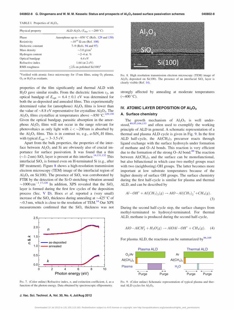
(�1–2 nm) SiOx layer is present at this interface.14,131,132 This
interfacial SiOx is formed even on H-terminated Si (e.g., after
HF treatment). Figure 8 shows a high-resolution transmission
electron microscopy (TEM) image of the interfacial region of
Al2O3 on Si(100). The presence of SiOx was corroborated by
FTIR by the detection of the Si-O stretching vibration around
�1000 cm�1.17,128 In addition, XPS revealed that the SiOx
layer is formed during the first few cycles of the deposition
process (Sec. V D). Hoex et al. reported a (very small)
increase of the SiOx thickness during annealing at �425 C of
�0.3 nm, which is close to the resolution of TEM.14 Our XPS
measurements confirmed that the SiOx thickness was not
strongly affected by annealing at moderate temperatures
(�400 C).
IV. ATOMIC LAYER DEPOSITION OF Al2O3
A. Surface chemistry
The growth mechanism of Al2O3 is well under-
stood,89,93,104,133 and often used to exemplify the working
principle of ALD in general. A schematic representation of a
thermal and plasma ALD cycle is given in Fig. 9. In the first
ALD half-cycle, the Al(CH3)3 precursor reacts through
ligand exchange with the surface hydroxyls under formation
of methane and O–Al bonds. This reaction is very efficient
due to the formation of the strong O–Al bond.89 The reaction
between Al(CH3)3 and the surface can be monofunctional,
but also bifunctional in which case two methyl groups react
with two (neighboring) OH groups. The latter becomes more
important at low substrate temperatures because of the
higher density of surface OH groups. The surface chemistry
during the first half-cycle is similar for plasma and thermal
ALD, and can be described by
Al�OH þAlðCH3Þ3ðgÞ ! AlO�AlðCH3Þ2þCH4ðgÞ:
(3)
During the second half-cycle step, the surface changes from
methyl-terminated to hydroxyl-terminated. For thermal
ALD, methane is produced during the second half-cycle,
AlO�AlCH3 þ H2OðgÞ ! AlOAl�OH þ CH4ðgÞ: (4)
For plasma ALD, the reactions can be summarized by96,105
0 2 4 6 8 100.0
0.5
1.0
1.5
2.0
2.5
k
as-depositedannealed
n&
k
Photon energy (eV)
n
FIG. 7. (Color online) Refractive index, n, and extinction coefficient, k, as a
function of the photon energy. Data obtained by spectroscopic ellipsometry.
FIG. 8. High resolution transmission electron microscopy (TEM) image of
Al2O3 deposited on Si(100). The presence of an interfacial SiOx layer is
clearly visible (Ref. 14).
Plasma ALD Thermal ALDPlasma ALDO2/Ar
Al(CH3)3
Thermal ALDAr
Al(CH3)3
Plasma
Purge
H2O
Purge Purge Purge
FIG. 9. (Color online) Schematic representation of typical plasma and ther-
mal ALD cycles for Al2O3.
TABLE I. Properties of Al2O3.
Physical property ALD Al2O3 (Tdep ¼ �200 C)
Phase Amorphous up to �850 C (Refs. 129 and 130)
Resistivity �1016 X cm (Ref. 108)
Dielectric constant 7–9 (Refs. 94 and 97)
Mass density �3.0 g/cm3
Hydrogen content �2–4 at. %
Optical bandgap 6.4 eV
Refractive index 1.64 (at 2 eV)
RMS roughness �2A on polished Si(100)a
aVerified with atomic force microscopy for 15 nm films, using O2 plasma,
O3 or H2O as oxidants.
040802-8 G. Dingemans and W. M. M. Kessels: Status and prospects of Al2O3-based surface passivation schemes 040802-8
J. Vac. Sci. Technol. A, Vol. 30, No. 4, Jul/Aug 2012
Downloaded 10 Jul 2012 to 131.155.113.183. Redistribution subject to AVS license or copyright; see http://avspublications.org/jvsta/about/rights_and_permissions

AlO�AlCH3þ4OðgÞ!AlOAl�OH þH2OðgÞþCOxðgÞ:(5)
Note that the formation of the H2O by-product during the
plasma step can give rise to a secondary reaction pathway.96
In addition to H2O and an O2 plasma, O3 also can be used
as coreactant. The reaction chemistry during O3-based ALD
appeared to be more complex than the H2O and O2–plasma-
based process (see, for example, Refs. 103–105).
Depending on the length of each of the steps in the ALD
cycle (Fig. 9), subsaturated growth, true ALD growth, or
ALD growth with a parasitic CVD component takes place.
The latter refers to a growth process that is not fully self-
limiting. A true, saturated ALD process is obtained when an
increase in the duration of the precursor and oxidant expo-
sure times, in conjunction with sufficiently long purge steps,
does not produce a higher growth per cycle (GPC). Under
such circumstances, the deposition is highly uniform and
conformal. Figure 10 shows that the thickness increases line-
arly with the number of cycles without apparent growth
delay for deposition on Si(100). The associated growth rates
were 1.0 A/cycle (thermal ALD) and 1.1 A/cycle (plasma
ALD) for Tdep¼ �250 C. Note that these values are below
the approximate thickness of a monolayer (�0.3 nm), which
can be attributed to incomplete surface OH coverage and
steric hindrance effects of the precursor molecules.
B. ALD process parameters
The influence of the relevant ALD parameters on the
GPC of Al2O3 is shown in Fig. 11, comparing thermal ALD
and plasma ALD. The TMA dosing time had virtually no
effect on the growth process in our reactor configuration
(Oxford Instruments OpAL). For dosing times of 10 ms and
above, saturated ALD growth was observed for both meth-
ods. However, the purge time after the Al(CH3)3 dosing
strongly influenced the growth process. Figure 11 shows that
purge times <�3 s gave rise to higher GPC values for
plasma and thermal ALD. In addition, short purge times led
to a decrease in refractive index (n ¼ �1.61 vs 1.64 for a
true ALD process) and corresponding decrease in mass den-
sity of the Al2O3 films. A parasitic CVD growth component
also produces film nonuniformity and is expected to impair
the conformality of ALD. The minimum purge times
required after the Al(CH3)3 precursor injection are closely
related to the gas residence time. For short purge times, a
fraction of Al(CH3)3 precursor remains in the reactor and
can react with the oxidant introduced in the subsequent oxi-
dation half-cycle.
Whether parasitic CVD reactions occur can be detected
by optical emission spectroscopy measurements during
plasma ALD. Figure 12 shows the presence of CO*, H*, and
OH* emission in the plasma.134 When the spectrum is
recorded after a sufficiently long purge time, the emission
associated with C and H fragments can only originate from a
monolayer of –CH3 ligands at the growth interface. How-
ever, when reducing the purge time below 3.5 s, we observe
an increase in the emission of CO*, H*, and OH* as shown in
Fig. 12(b). This is indicative of the dissociation of residual
Al(CH3)3 in the plasma and corresponds well with the
observed higher GPC values.
Regarding the second half-cycle, a saturated ALD process
was obtained already for short H2O dosing times (�10–20 ms),
which also led to high refractive index values of�1.64. A slight
increase of the GPC was, however, observed for longer H2O
dosing times. This is typically observed for thermal ALD at rel-
atively low substrate temperatures and is referred to as “soft sat-
uration.”94 The plasma time had a more pronounced effect on
the growth process. Plasma times <2 s clearly led to subsatu-
rated growth. Under these circumstances the total flux of oxygen
radicals during the oxidation half-cycle is insufficient to remove
all the precursor ligands and restore the surface with OH groups.
The plasma time can therefore be associated with the rate of the
surface chemical reactions. The refractive index was also
observed to drop for short plasma times, which is indicative of
the incorporation of impurities into the material. Moreover, it
was observed that subsaturated growth led to a significant dete-
rioration of the thickness uniformity, especially at the edges of
the substrate holder. The final purge step in the ALD cycle
serves to remove the traces of the oxidant and reaction products
left in the reactor. Figure 11 demonstrates that significant purg-
ing after plasma exposure was not required, while after H2O
dosing, purge times �1 s were important to avoid parasitic
CVD reactions. This implies that the very small amount of H2O
produced during the O2 plasma step did not lead to significant
reactions with the Al(CH3)3 precursor introduced in the subse-
quent step. This may change at lower deposition temperatures,
for which generally longer plasma purge times are required.
For the optimized ALD processes in the single-wafer re-
actor (Oxford Instruments OpAL), nonuniformities of 1.5%
and 4.3% were obtained for thermal and plasma ALD for
wafers 200 mm in diameter. For similar wafer sizes, values
of <2% have been reported for thermal and plasma ALD
before.97 The slight nonuniformity of plasma ALD can be
attributed to a radial nonuniformity of the plasma species
and can be decreased when using smaller wafers.
C. Substrate temperature
The substrate temperature is the most important parame-
ter affecting the growth rate and, as discussed in Sec. III B,
0 100 200 300 400 5000
10
20
30
40
50 Plasma ALD Thermal ALD
Thic
knes
s (n
m)
Number of cycles
FIG. 10. (Color online) Al2O3 film thickness as a function of the number of
ALD cycles (Tdep ¼ 250 C).
040802-9 G. Dingemans and W. M. M. Kessels: Status and prospects of Al2O3-based surface passivation schemes 040802-9
JVST A - Vacuum, Surfaces, and Films
Downloaded 10 Jul 2012 to 131.155.113.183. Redistribution subject to AVS license or copyright; see http://avspublications.org/jvsta/about/rights_and_permissions

the material properties of ALD Al2O3 films. Figure 13 shows
that the influence of Tdep on film growth is markedly differ-
ent for plasma and thermal ALD.97–99 For plasma ALD, the
GPC and the number of Al atoms deposited per cycle
decreases with increasing Tdep. This trend can be attributed
to a lower OH surface coverage at higher Tdep, due to ther-
mally activated dehydroxylation reactions under formation
of H2O.92 For thermal ALD, an increase in the growth rate
was observed for increasing Tdep up to �250 C, whereas for
Tdep> 250 C the trend was similar to plasma ALD. This dif-
ference between thermal and plasma ALD at low Tdep can be
explained by a lower reactivity of H2O at low substrate tem-
peratures. In contrast, the reactivity of the O2 plasma is not
controlled by the temperature. From a technological point of
view, it is important to note that the purge times to remove
H2O from the reactor increase drastically with decreasing
300 400 500 600 700 800 0 2 4 6 8
(b)
Purge (s)
CO*
Hα
OH*
OES
sig
nal
Wavelength (nm)
OH*
Hα
O*
CO*
Hβ
(a)
FIG. 12. (Color online) (a) Optical emission spectroscopy spectrum recorded
during plasma ALD. (b) Emission intensity of OH, H*, and CO* as a func-
tion of the preceding Al(CH3)3 purge length. Every data point represents a
separate measurement during the initial stages of plasma operation. Note
that for the purge time of 0 s, the plasma was switched on directly after the
precursor dose.
0 100 200 300 4000123456
0.0
0.1
0.2
(b)
Substrate temperature (oC)
Plasma ALD Thermal ALD
# A
l ato
ms
per c
ycle
(
1015
cm
-2)
G
row
th ra
te (n
m/c
ycle
)
(a)
FIG. 13. (Color online) Influence of the substrate temperature on the growth
per cycle in terms of (a) film thickness and (b) Al atoms deposited (Refs. 98
and 99). The latter was determined by RBS measurements.
0 20 40 60 80 1000.00
0.05
0.10
0.15
0.20
Gro
wth
per
Cyc
le (n
m/c
ycle
)
Dose time (ms)0 1 2 3 4 5
Purge time (s)
0 1 2 3 4 5
(b)
Plasma time (s)
(a)
Subsaturation
0 1 2 3
CVD
Purge time (s)
0 20 40 60 80 1000.00
0.05
0.10
0.15
0.20
Gro
wth
per
Cyc
le (n
m/c
ycle
)
Dose time (ms)0 1 2 3 4 5
Purge time (s)
CVD
0 20 40 60 80
Subsaturation CVD
H2O dose time (ms)0 1 2 3
Purge time (s)
FIG. 11. (Color online) Growth per cycle (GPC) as a function of the length of successive ALD steps for (a) thermal ALD and (b) plasma ALD. The films were
deposited in an Oxford Instruments OpAL reactor (Tdep ¼ 250 C). The nonvaried parameters (purge and dose times) were sufficiently long to be compatible
with saturated ALD growth and did not affect the influence of the varied parameter on the GPC.
040802-10 G. Dingemans and W. M. M. Kessels: Status and prospects of Al2O3-based surface passivation schemes 040802-10
J. Vac. Sci. Technol. A, Vol. 30, No. 4, Jul/Aug 2012
Downloaded 10 Jul 2012 to 131.155.113.183. Redistribution subject to AVS license or copyright; see http://avspublications.org/jvsta/about/rights_and_permissions
Tdep. Plasma ALD is therefore generally preferred over ther-
mal ALD for low-temperature applications (<150 C).
V. SURFACE PASSIVATION BY Al2O3
A. Passivation performance
Very low surface recombination velocities Seff< 5 cm/s
have been reported for Al2O3 on low-resistivity p-type and
n-type Si (typically, 1–4 X cm) after annealing at moderate
temperatures.14,15,40,98,135,136 In addition, for boron-doped
emitters ALD Al2O3 resulted in very low emitter saturation
current densities of J0,e � 10 and 30 fA/cm2 for >100 and
54 X/sq sheet resistances, respectively.137 In other studies,
Al2O3 passivation has shown to be compatible with implied
Voc values up to 700 mV (90 X/sq emitter).40,138 Also for
screen-printed Al-pþ-emitters comparatively low J0,e values
(�160 fA/cm2) have been obtained.139 The level of passiva-
tion achieved by Al2O3 for pþ surfaces was higher than
obtained by thermal SiO2 and a-Si:H and significantly higher
than by SiNx.16,137 This can be explained by the differences
in strength and polarity of the fixed charges present in the
passivation schemes. Possibly, differences in the capture
cross section ratios—a relatively lower rn/rp is beneficial
for pþ passivation—may contribute as well (see Sec. II A).
For nþ emitters, it is expected that the negative Qf of Al2O3
will not contribute to optimal passivation properties when
compared to SiNx containing positive charges. Preliminary
measurements have indeed revealed significantly higher J0,e
values for Al2O3 (�170 fA/cm2) than for SiNx (�62 fA/cm2)
on 62 X/sq nþ emitters.140 Another report has shown that
implied Voc values between �640 and �680 mV can be
achieved for sheet resistances between 20 and �100 X/sq
using plasma ALD Al2O3.141 It was argued that the low
interface defect density induced by Al2O3 is primarily re-
sponsible for the passivation of nþ emitters with low sheet
resistances (<�100 X/sq).
Prior to deposition of the Al2O3 films on lifetime samples,
the native oxide is generally removed from the wafers by treat-
ment in diluted HF (e.g., 1%) followed by rinsing in de-ionized-
H2O and drying (e.g., in an N2 flow). The time between this
cleaning step and film deposition is not a critical parameter. In
addition, even surface chemical treatments (e.g., treatment in
HNO3) that result in a chemical oxide on the wafer surface can
be applied prior to Al2O3 deposition.54 To activate the passiva-
tion, annealing temperatures in the range of 350–450 C were
found to be optimal.135 Annealing can be simply carried out in
N2 environment, as a gas mixture containing H2 (i.e., forming
gas annealing) led to similar results. Annealing times between
10 and 30 min are generally applied. However, we verified that
annealing times of �1–2 min can already be sufficient to fully
activate the passivation performance of the films.
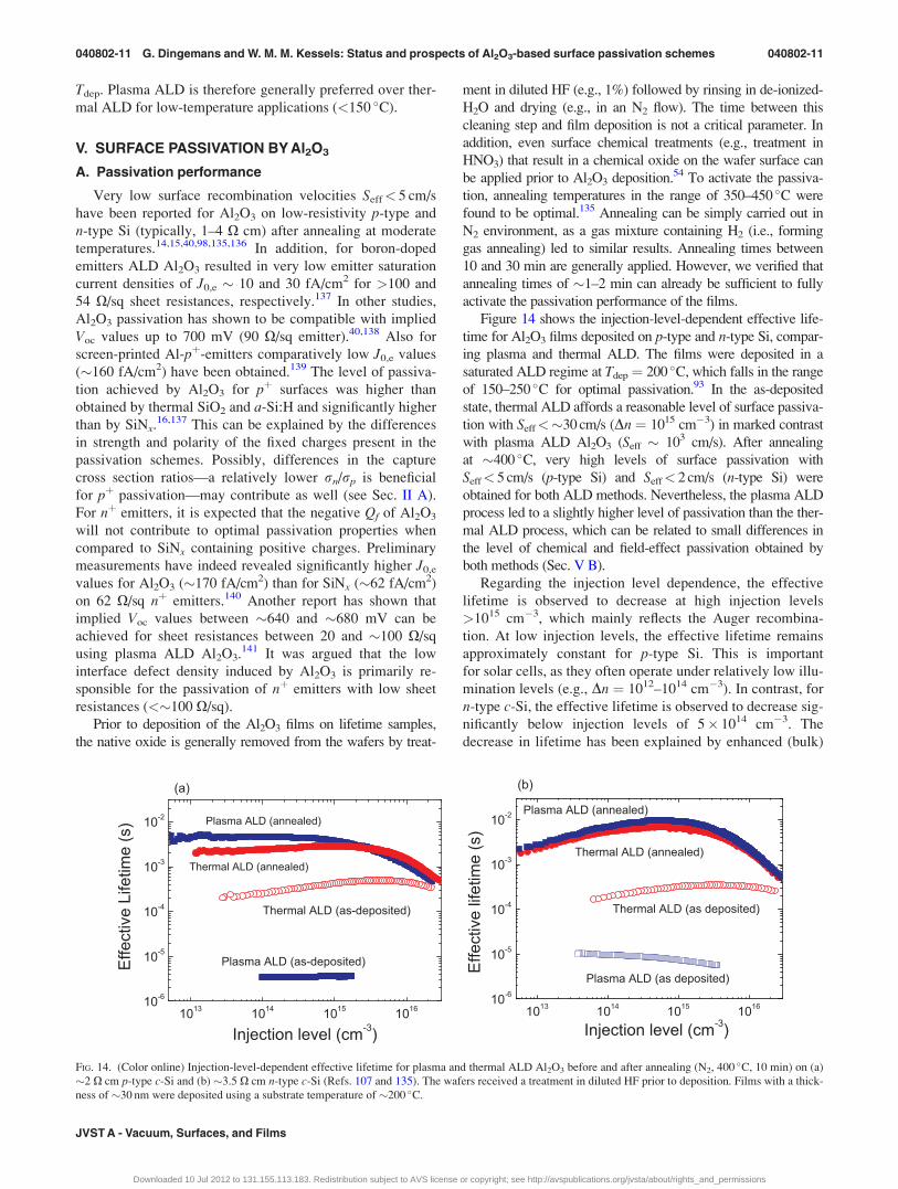
Figure 14 shows the injection-level-dependent effective life-
time for Al2O3 films deposited on p-type and n-type Si, compar-
ing plasma and thermal ALD. The films were deposited in a
saturated ALD regime at Tdep¼ 200 C, which falls in the range
of 150–250 C for optimal passivation.93 In the as-deposited
state, thermal ALD affords a reasonable level of surface passiva-
tion with Seff<�30 cm/s (Dn ¼ 1015 cm�3) in marked contrast
with plasma ALD Al2O3 (Seff � 103 cm/s). After annealing
at �400 C, very high levels of surface passivation with
Seff< 5 cm/s (p-type Si) and Seff< 2 cm/s (n-type Si) were
obtained for both ALD methods. Nevertheless, the plasma ALD
process led to a slightly higher level of passivation than the ther-
mal ALD process, which can be related to small differences in
the level of chemical and field-effect passivation obtained by
both methods (Sec. V B).
Regarding the injection level dependence, the effective
lifetime is observed to decrease at high injection levels
>1015 cm�3, which mainly reflects the Auger recombina-
tion. At low injection levels, the effective lifetime remains
approximately constant for p-type Si. This is important
for solar cells, as they often operate under relatively low illu-
mination levels (e.g., Dn ¼ 1012–1014 cm�3). In contrast, for
n-type c-Si, the effective lifetime is observed to decrease sig-
nificantly below injection levels of 5� 1014 cm�3. The
decrease in lifetime has been explained by enhanced (bulk)
1013 1014 1015 101610-6
10-5
10-4
10-3
10-2 Plasma ALD (annealed)
Plasma ALD (as-deposited)
Thermal ALD (as-deposited)
Effe
ctiv
e Li
fetim
e (s
)
Injection level (cm-3)
Thermal ALD (annealed)
(a)
1013 1014 1015 101610-6
10-5
10-4
10-3
10-2
Thermal ALD (annealed)
Thermal ALD (as deposited)
Effe
ctiv
e lif
etim
e (s
)
Injection level (cm-3)
Plasma ALD (as deposited)
Plasma ALD (annealed)
(b)
FIG. 14. (Color online) Injection-level-dependent effective lifetime for plasma and thermal ALD Al2O3 before and after annealing (N2, 400 C, 10 min) on (a)
�2 X cm p-type c-Si and (b) �3.5 X cm n-type c-Si (Refs. 107 and 135). The wafers received a treatment in diluted HF prior to deposition. Films with a thick-
ness of �30 nm were deposited using a substrate temperature of �200 C.
040802-11 G. Dingemans and W. M. M. Kessels: Status and prospects of Al2O3-based surface passivation schemes 040802-11
JVST A - Vacuum, Surfaces, and Films
Downloaded 10 Jul 2012 to 131.155.113.183. Redistribution subject to AVS license or copyright; see http://avspublications.org/jvsta/about/rights_and_permissions

recombination in the inversion layer induced by the negative
Qf.17,28,142 Further evidence for this hypothesis is provided
by the observation that the effective lifetime under low illu-
mination conditions could be improved by a significant
reduction in Qf.143
The influence of the ALD process parameters (i.e., dose
and purge times, see Fig. 11) on the passivation quality of as-
deposited and annealed Al2O3 films was also assessed. The
passivation performance appeared to be insensitive to varia-
tions in the process parameters (not shown), with the excep-
tion of the plasma time. Interestingly, a reduction in plasma
time led to a significant decrease in the Seff values for as-
deposited plasma ALD Al2O3 (Tdep ¼ 250 C). This can be
attributed to a detrimental impact of vacuum ultraviolet
(VUV) radiation from the plasma which is reduced for shorter
plasma times.107 Furthermore, it is important to note that a
pure ALD growth mode was not necessary for obtaining opti-
mal passivation. For example, a reduction in the Al(CH3)3
purge times from 3.5 to 0.5 s led to significantly higher
growth rates (GPC values of �1.8 A, see Fig. 11) without
compromising the passivation performance (Seff< 2 cm/s).
Nonetheless, conditions outside the ALD growth window are
expected to lead to an increase in thickness nonuniformity.
B. Effect of annealing on chemical and field-effectpassivation
Figure 15 shows the influence of annealing on the surface
passivation mechanisms of Al2O3 films synthesized by
plasma ALD and thermal ALD (using H2O). For thermal
ALD Al2O3, the key effect of annealing is the increase of Qf,
whereas for plasma ALD the chemical passivation improves
dramatically. The relatively low Dit value of �3� 1011
eV�1 cm�2 for as-deposited thermal ALD Al2O3 is consist-
ent with the moderate level of surface passivation obtained
prior to annealing (compare Fig. 14).107 This is in sharp con-
trast with plasma ALD, which did not provide passivation in
the as-deposited state despite the high value of Qf. It has
been shown that the high Dit values for as-deposited plasma
ALD Al2O3 are, at least partially, related to the exposure of
the surface to VUV radiation that is present in the
plasma.107,144 After annealing, both ALD processes resulted
in low Dit� 1� 1011 eV�1 cm�2.107,146,147 Also for films de-
posited by PECVD, similar low defect densities were
reported.145
Regarding the field-effect passivation, it is notable that
the thermal ALD Al2O3 films exhibited very low Qf values
of the order of 1011 cm�2 prior to annealing; in contrast to
plasma ALD with Qf of the order of 1012 cm�2. Also after
annealing, the highest Qf values have been reported for
Al2O3 synthesized by plasma ALD. Furthermore, it was veri-
fied that Qf was not critically dependent on the annealing
temperature (T ¼ 300–600 C), see Fig. 16. While an initial
increase is observed between T ¼ 300 and 400 C, Qf
appeared to be relatively independent of the annealing tem-
perature for T� 400 C. Similar observations were reported
by Benick et al.146
In general, the Qf values that are reported for Al2O3 in vari-
ous studies fall in the range of (2–13)� 1012 cm�2 after anneal-
ing at moderate temperatures.12,16,98,107,123,124,127,146,147 Note
that these films all afforded low Seff values<�10 cm/s.
Although the relevant material or processing parameters
responsible for the variations in Qf have not been fully identi-
fied, it was reported that the deposition temperature during
ALD can affect the passivation mechanisms of the films. It was
found that a variation in Tdep between 150 and 300 C also gave
rise to a variation in Qf between 6 and 3.5� 1012 cm�2.148
C. Effect of film thickness
A key benefit of ALD is the ability to deposit ultrathin
films. For thermal ALD, a correlation between film thickness
and as-deposited surface passivation performance was
found.135 This effect may be attributed to a small “in situannealing effect” taking place in the ALD reactor (at a depo-
sition temperature of 200 C) during prolonged processing
time. More interesting is the thickness dependence after
annealing. A constant high level of surface passivation could
be maintained down to approximately 5 and 10 nm, for
plasma and thermal ALD, respectively.135,147 It has been
established that the cause of the deterioration is a decrease in
FIG. 15. (Color online) Influence of annealing on the negative fixed charge
density, Qf, and interface defect density at midgap, Dit, for plasma and ther-
mal ALD Al2O3 films. In the various studies annealing took place at temper-
atures of �400 C.
200 300 400 500 600
1011
1012
1013
Thermal ALD
Neg
ativ
e Q
f (cm
-2)
Annealing temperature (oC)
Plasma ALD
as-d
epos
ited
FIG. 16. (Color online) Negative fixed charge density Qf vs annealing tem-
perature (N2, 10 min) for plasma and thermal ALD Al2O3 films. Qf was
determined from C–V measurements. Film thickness was � 30 nm.
040802-12 G. Dingemans and W. M. M. Kessels: Status and prospects of Al2O3-based surface passivation schemes 040802-12
J. Vac. Sci. Technol. A, Vol. 30, No. 4, Jul/Aug 2012
Downloaded 10 Jul 2012 to 131.155.113.183. Redistribution subject to AVS license or copyright; see http://avspublications.org/jvsta/about/rights_and_permissions
the chemical passivation.145,149,150 Measurements by the
noncontacting technique of secondary-harmonic spectros-
copy have shown that the field-effect passivation remained
constant while decreasing the film thickness to 2 nm.150 This
is consistent with the fixed negative charges being located
near the SiOx/Al2O3 interface. Similar conclusions have
been drawn from C–V measurements.151,152
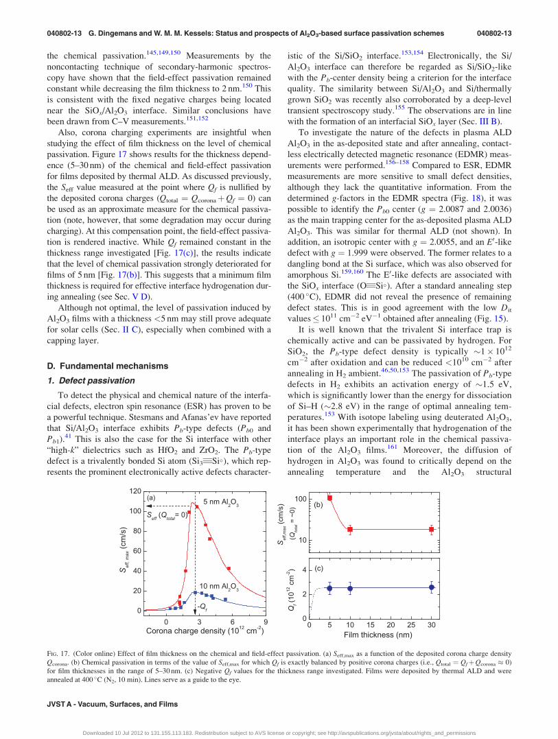
Also, corona charging experiments are insightful when
studying the effect of film thickness on the level of chemical
passivation. Figure 17 shows results for the thickness depend-
ence (5–30 nm) of the chemical and field-effect passivation
for films deposited by thermal ALD. As discussed previously,
the Seff value measured at the point where Qf is nullified by
the deposited corona charges (Qtotal ¼ QcoronaþQf ¼ 0) can
be used as an approximate measure for the chemical passiva-
tion (note, however, that some degradation may occur during
charging). At this compensation point, the field-effect passiva-
tion is rendered inactive. While Qf remained constant in the
thickness range investigated [Fig. 17(c)], the results indicate
that the level of chemical passivation strongly deteriorated for
films of 5 nm [Fig. 17(b)]. This suggests that a minimum film
thickness is required for effective interface hydrogenation dur-
ing annealing (see Sec. V D).
Although not optimal, the level of passivation induced by
Al2O3 films with a thickness <5 nm may still prove adequate
for solar cells (Sec. II C), especially when combined with a
capping layer.
D. Fundamental mechanisms
1. Defect passivation
To detect the physical and chemical nature of the interfa-
cial defects, electron spin resonance (ESR) has proven to be
a powerful technique. Stesmans and Afanas’ev have reported
that Si/Al2O3 interface exhibits Pb-type defects (Pb0 and
Pb1).41 This is also the case for the Si interface with other
“high-k” dielectrics such as HfO2 and ZrO2. The Pb-type
defect is a trivalently bonded Si atom (Si3 Si), which rep-
resents the prominent electronically active defects character-
istic of the Si/SiO2 interface.153,154 Electronically, the Si/
Al2O3 interface can therefore be regarded as Si/SiO2-like
with the Pb-center density being a criterion for the interface
quality. The similarity between Si/Al2O3 and Si/thermally
grown SiO2 was recently also corroborated by a deep-level
transient spectroscopy study.155 The observations are in line
with the formation of an interfacial SiOx layer (Sec. III B).
To investigate the nature of the defects in plasma ALD
Al2O3 in the as-deposited state and after annealing, contact-
less electrically detected magnetic resonance (EDMR) meas-
urements were performed.156–158 Compared to ESR, EDMR
measurements are more sensitive to small defect densities,
although they lack the quantitative information. From the
determined g-factors in the EDMR spectra (Fig. 18), it was
possible to identify the Pb0 center (g ¼ 2.0087 and 2.0036)
as the main trapping center for the as-deposited plasma ALD
Al2O3. This was similar for thermal ALD (not shown). In
addition, an isotropic center with g ¼ 2.0055, and an E0-like
defect with g ¼ 1.999 were observed. The former relates to a
dangling bond at the Si surface, which was also observed for
amorphous Si.159,160 The E0-like defects are associated with
the SiOx interface (O Si). After a standard annealing step
(400 C), EDMR did not reveal the presence of remaining
defect states. This is in good agreement with the low Dit
values� 1011 cm�2 eV�1 obtained after annealing (Fig. 15).
It is well known that the trivalent Si interface trap is
chemically active and can be passivated by hydrogen. For
SiO2, the Pb-type defect density is typically �1� 1012
cm�2 after oxidation and can be reduced <1010 cm�2 after
annealing in H2 ambient.46,50,153 The passivation of Pb-type
defects in H2 exhibits an activation energy of �1.5 eV,
which is significantly lower than the energy for dissociation
of Si–H (�2.8 eV) in the range of optimal annealing tem-
peratures.153 With isotope labeling using deuterated Al2O3,
it has been shown experimentally that hydrogenation of the
interface plays an important role in the chemical passiva-
tion of the Al2O3 films.161 Moreover, the diffusion of
hydrogen in Al2O3 was found to critically depend on the
annealing temperature and the Al2O3 structural
0 3 6 90
20
40
60
80
100
120
-Qf
10 nm Al2O3
S eff,
max
(cm
/s)
Corona charge density (1012 cm-2)
Seff (Qtotal= 0)
5 nm Al2O3(a)
0 5 10 15 20 25 300
2
4 (c)
Qf (
1012
cm
-2)
Film thickness (nm)
(b)
10
100
Sef
f,max
(cm
/s)
(Qto
tal =
~0)
FIG. 17. (Color online) Effect of film thickness on the chemical and field-effect passivation. (a) Seff,max as a function of the deposited corona charge density
Qcorona. (b) Chemical passivation in terms of the value of Seff,max for which Qf is exactly balanced by positive corona charges (i.e., Qtotal ¼ QfþQcorona � 0)
for film thicknesses in the range of 5–30 nm. (c) Negative Qf values for the thickness range investigated. Films were deposited by thermal ALD and were
annealed at 400 C (N2, 10 min). Lines serve as a guide to the eye.
040802-13 G. Dingemans and W. M. M. Kessels: Status and prospects of Al2O3-based surface passivation schemes 040802-13
JVST A - Vacuum, Surfaces, and Films
Downloaded 10 Jul 2012 to 131.155.113.183. Redistribution subject to AVS license or copyright; see http://avspublications.org/jvsta/about/rights_and_permissions

properties.162 For films that exhibited either a low mass
density (and high hydrogen content) or a very low initial
hydrogen content (and a high mass density), the passivation
was less thermally stable at temperatures of �600 C com-
pared to films with intermediate properties. Finally it is
speculated that, apart from the interface hydrogenation, the
chemical passivation may also be influenced by film relaxa-
tion, Si–O bond rearrangements, and some additional inter-
facial oxide growth during annealing.
2. Negative charge formation
The microscopic origin of the defect states in the Si–
Al2O3 system that lead to negative Qf has not been clearly
established (see the discussion in Ref. 17). Moreover, dedi-
cated theoretical or experimental work on this topic has not
yet been carried out in the context of field-effect passivation.
However, in a broader context, defects in Al2O3, and espe-
cially in other (high-k) metal oxides, have been studied for
their important role in metal–oxide–semiconductor applica-
tions. It is well known that the origin of the charge traps are
(ionized) point defects,163–166 with candidates such as (oxy-
gen or metal atom) vacancies and interstitials. The latter
may also include extrinsic defects, such as interstitial hydro-
gen.167 The defects in these ionic metal-oxides are different
from those in thermally-grown SiO2.
Various simulation studies have identified the point defects
in Al2O3, i.e., the O vacancy, the O interstitial, the Al va-
cancy, and the Al interstitial, and their energetic positions in
the bandgap.164,168–170 Liu et al. have provided evidence that
the O vacancy is responsible for transport and trapping prop-
erties.164 However, it is not likely responsible for negative
charge. In a simulation study, Matsunaga et al. have reported
that the Al vacancy (VAl) and the O interstitial (Oi) can be
charged negatively.168 VAl was found to be stable in the �3
state, and Oi in the �2 state.168,169 Using more advanced sim-
ulations, Weber et al. have recently analyzed the defects in
Al2O3 in the context of III–V electronics.169 They found that
VAl and Oi produce levels in the Al2O3 bandgap belowmidgap. Both defects are therefore likely candidates to trap
negative fixed charge in, e.g., the InGaAs/Al2O3 system which
has a valence band offset of Ev � 3 eV compared to the
Al2O3 valence band maximum. As Ev� 3 eV for Si,164,171,172
we may expect that the negative fixed charge in the Si/Al2O3
system has a similar origin.
Experimentally, however, it is difficult to determine
unambiguously the presence and type of point defects in the
bulk of ultrathin films. Moreover, the concentration and type
of defects that form near the Si/Al2O3 interface may differ
from the bulk. When the negative charge is related to the
presence of VAl and Oi defects, a slightly oxygen-rich struc-
ture in proximity of the Si interface would be expected. In
agreement with this, Shin et al. have demonstrated that nega-
tive fixed charges were indeed correlated with the presence
of an O-rich region near the interface for InGaAs/Al2O3
MOS structures.170 Also for the Si/Al2O3 system, depth-
dependent structural properties have been reported by
Kimoto et al.173 Both tetrahedrally and octahedrally coordi-
nated Al atoms exist in Al2O3, but the former appeared to be
more dominant near the surface.
Regarding the stoichiometry of the ALD films, an O/Al
ratio very close to �1.5 was determined by RBS for a film
deposited using 250 ALD cycles (Tdep� 200 C).98 How-
ever, due to the presence of a small amount of OH groups
(�1–3 at. %) it is expected that the films are slightly O-rich.
To investigate whether the stoichiometry of Al2O3 is thick-
ness dependent, XPS spectra were recorded for films grown
using 10 cycles (�1.2 nm) and 100 cycles (�12 nm). The Al
2p peak is sensitive to structural variations in the Al2O3
films, and it was found to consist of multiple contributions
for the ultrathin 1.2 nm film. The most prominent contribu-
tions can be assigned to an Al2O3 structure (�74.4 eV) and
the presence of Al–OH bonds (�75.6 eV),174 see Fig. 19(b).
At the surface, carbon was detected [Fig. 19(c)], which also
appears in the Al 2p spectrum. To obtain a semiquantitative
analysis of the atomic Al and O density for ultrathin Al2O3
films, the O contribution originating from the carbonates on
the surface and from the interfacial oxide is significant and
has to be corrected for. Moreover, an adsorbed H2O layer on
the surface can also contribute.175 This leads to an inherent
uncertainty in the O/Al ratio for very thin films. Also for
thicker films, a sensitivity factor is required to calibrate
the O/Al ratio as determined by XPS to the more precise
value determined by RBS. Figure 19(d) shows that small
variations in the stoichiometry near the interface, most likely
a higher oxygen concentration, may exist. In contrast, a
more dramatic change in stoichiometry near the interface
was recently suggested by Werner et al., with the O/Al ratio
reaching a value as high as �8, as was inferred from XPS
measurements.147
However, in this context, it is relevant to consider that the
number of defect states near the interface that is required to
account for Qf is relatively small. Using atomic densities
obtained by RBS, we can estimate the number density of
“Al2O3 units” to be approximately 7� 1014 units/cm2 at the
SiOx/Al2O3 interface. Therefore, for a fixed charge density of
3220 3240 3260 3280 3300 3320-3
-2
-1
0
1
2
g = 1.999
g = 2.0055
g = 2.0036
g = 2.0087
annealed(400 oC, N2)
ED
MR
spec
trum
ΔV(1
0-4V
)
Magnetic field (G)
T=4.5K, 180 mW, 9.16 GHz
H II [011]
as-deposited
FIG. 18. (Color online) Electrically detected magnetic resonance (EDMR)
spectra obtained for plasma ALD Al2O3 films deposited on Si(100). As-
deposited and annealed samples were compared.
040802-14 G. Dingemans and W. M. M. Kessels: Status and prospects of Al2O3-based surface passivation schemes 040802-14
J. Vac. Sci. Technol. A, Vol. 30, No. 4, Jul/Aug 2012
Downloaded 10 Jul 2012 to 131.155.113.183. Redistribution subject to AVS license or copyright; see http://avspublications.org/jvsta/about/rights_and_permissions

7� 1012 charges/cm2, we find that only one “surface charge” is
present for every 102 Al2O3 units. Thus, a very large deviation
from stoichiometry appears not to be a prerequisite to account
for the typical negative fixed charge densities of Al2O3.
Another important issue is the role of charging of defect
states. The charge state of an (ionized) defect can be changed
by electron (or hole) injection into the conduction (or va-
lence) band of the dielectric and by tunneling from the
dielectric into the substrate or from the dielectric surface
into the metal (gate).176,177 For the Si/Al2O3 system, there
are some indications that charge injection from Si into Al2O3
may play a role in the formation of the negative Qf. Second-
harmonic generation experiments have demonstrated that Qf
can increase under influence of laser irradiation.172 This is
consistent with (multi-) photon-induced charge injection
from Si into preexistent defect states at the SiOx/Al2O3 inter-
face. In addition, we have observed a hysteresis during co-
rona charging experiments that is consistent with a charge
injection phenomenon. For annealed Al2O3 samples, the
fixed charge density was observed to increase by (1–2)
� 1012 cm�2 after deposition of positive corona charges
(�1013 cm�2) on the Al2O3 surface (not shown). The net
positive charge may attract electrons from the Si wafer into
defect states at the SiOx/Al2O3 interface. In addition, it has
been demonstrated that an increase in the SiO2 interlayer
thickness over the range of 1–30 nm gave rise to a decrease
in negative Qf.69,143 For instance, flatband conditions were
observed for an ALD SiO2 interlayer thickness of �5 nm.143
The simplest explanation is that the SiO2 acts as a barrier,
reducing charge injection from the Si substrate into defect
states at the SiO2/Al2O3 interface.
In conclusion, simulations and experiments have provided
evidence that the negative charge at the SiO2/Al2O3 interface
may be related to VAl and Oi defects. Charge injection phe-
nomenon across the interface may play a role in the forma-
tion of the negative charge associated with these defects. It
is important to point out that also other mechanisms can con-
tribute to negative charges, and that more research is
required to draw final conclusions.
VI. IMPLEMENTATION IN SOLAR CELLS
A. Stability
1. UV stability
The ultraviolet (UV) stability of a passivation layer is im-
portant when applied at the front side of a solar cell. With an
optical bandgap of �6.4 eV, amorphous Al2O3 is transparent
for the UV radiation in the solar spectrum. The surface passi-
vation induced by Al2O3 was not found to degrade during
the UV exposure of an Hg lamp (�254 nm). In fact, in some
cases the effective lifetime of an Al2O3-passivated wafer
exposed to UV light was even observed to increase by
�40%.178 This was tentatively explained by an increase in
Qf by photon-induced charge injection from the Si substrate.
Other reports have shown that during light soaking the passi-
vation performance remained stable.179
2. Firing stability
When Al2O3 surface passivation films are implemented in
screen-printed solar cells, the thermal stability of the films
during high-temperature firing processes (>800 C) is crucial.
The impact of direct firing and firing after a preceding low-
temperature annealing step on the passivation properties of
Al2O3 has been evaluated.40,136,178 The reports show that the
level of passivation by Al2O3 decreases, but that its thermal
stability is generally sufficient for application in screen-
printed solar cells. On the other hand, the exact level of passi-
vation that can be expected after firing is strongly dependent
on the peak temperature and the duration of the firing step.
For low resistivity n- and p-type c-Si, Seff< 14 and
25 cm/s have been reported after annealing (400 C) and sub-
sequent firing (800 C).178,180 After direct firing at 750 C,
an Seff value of �20 cm/s could be achieved for p-type Si.40
Moreover, a good thermal stability was obtained for the pas-
sivation of pþ emitters.40,138,181 The latter also appeared to
be less sensitive to the peak temperature than the passivation
of low resistivity Si wafers. For instance, the level of passi-
vation of a 90 X/sq. pþ emitter was compatible with
108 105 102 99 960.0
0.2
0.4
0.6
0.8
1.0
80 75 700.0
0.1
0.2
292 288 284 2800.0
0.1
0.2
0 100 200 3000
2
4
6
XP
S s
igna
l
Binding energy (eV)
Si 2p(a)
Al2O3
(d)
(c)
(b) as-grown annealed
Si-Si
Si-O
Al 2pAl-OH
Binding energy (eV)
C 1s
O/A
l rat
io
C-O
Number of ALD cycles
FIG. 19. (Color online) (a)–(c) X-ray photoelectron spectroscopy (XPS) applied to an ultrathin Al2O3 film synthesized using 10 plasma ALD cycles on HF-last
Si(100). Data are obtained before and after annealing (400 C, 10 min, N2). (d) Estimate of the O/Al ratio for films deposited using 10 and 100 cycles (XPS
measurement) and 250 cycles (Rutherford backscattering spectroscopy measurement).
040802-15 G. Dingemans and W. M. M. Kessels: Status and prospects of Al2O3-based surface passivation schemes 040802-15
JVST A - Vacuum, Surfaces, and Films
Downloaded 10 Jul 2012 to 131.155.113.183. Redistribution subject to AVS license or copyright; see http://avspublications.org/jvsta/about/rights_and_permissions
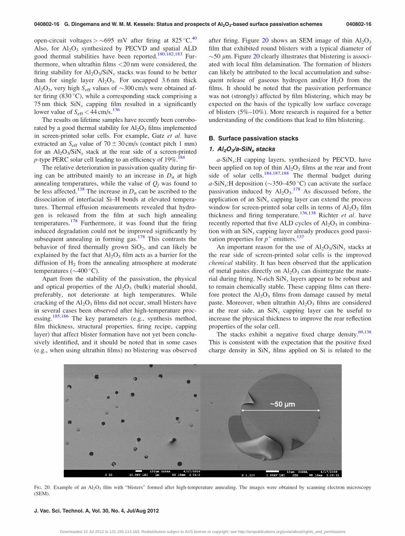
open-circuit voltages>�695 mV after firing at 825 C.40
Also, for Al2O3 synthesized by PECVD and spatial ALD
good thermal stabilities have been reported.180,182,183 Fur-
thermore, when ultrathin films <20 nm were considered, the
firing stability for Al2O3/SiNx stacks was found to be better
than for single layer Al2O3. For uncapped 3.6 nm thick
Al2O3, very high Seff values of �300 cm/s were obtained af-
ter firing (830 C), while a corresponding stack comprising a
75 nm thick SiNx capping film resulted in a significantly
lower value of Seff< 44 cm/s.136
The results on lifetime samples have recently been corrobo-
rated by a good thermal stability for Al2O3 films implemented
in screen-printed solar cells. For example, Gatz et al. have
extracted an Seff value of 70 6 30 cm/s (contact pitch 1 mm)
for an Al2O3/SiNx stack at the rear side of a screen-printed
p-type PERC solar cell leading to an efficiency of 19%.184
The relative deterioration in passivation quality during fir-
ing can be attributed mainly to an increase in Dit at high
annealing temperatures, while the value of Qf was found to
be less affected.138 The increase in Dit can be ascribed to the
dissociation of interfacial Si–H bonds at elevated tempera-
tures. Thermal effusion measurements revealed that hydro-
gen is released from the film at such high annealing
temperatures.178 Furthermore, it was found that the firing
induced degradation could not be improved significantly by
subsequent annealing in forming gas.178 This contrasts the
behavior of fired thermally grown SiO2, and can likely be
explained by the fact that Al2O3 film acts as a barrier for the
diffusion of H2 from the annealing atmosphere at moderate
temperatures (�400 C).
Apart from the stability of the passivation, the physical
and optical properties of the Al2O3 (bulk) material should,
preferably, not deteriorate at high temperatures. While
cracking of the Al2O3 films did not occur, small blisters have
in several cases been observed after high-temperature proc-
essing.185,186 The key parameters (e.g., synthesis method,
film thickness, structural properties, firing recipe, capping
layer) that affect blister formation have not yet been conclu-
sively identified, and it should be noted that in some cases
(e.g., when using ultrathin films) no blistering was observed
after firing. Figure 20 shows an SEM image of thin Al2O3
film that exhibited round blisters with a typical diameter of
�50 lm. Figure 20 clearly illustrates that blistering is associ-
ated with local film delamination. The formation of blisters
can likely be attributed to the local accumulation and subse-
quent release of gaseous hydrogen and/or H2O from the
films. It should be noted that the passivation performance
was not (strongly) affected by film blistering, which may be
expected on the basis of the typically low surface coverage
of blisters (5%–10%). More research is required for a better
understanding of the conditions that lead to film blistering.
B. Surface passivation stacks
1. Al2O3/a-SiNx stacks
a-SiNx:H capping layers, synthesized by PECVD, have
been applied on top of thin Al2O3 films at the rear and front
side of solar cells.184,187,188 The thermal budget during
a-SiNx:H deposition (�350–450 C) can activate the surface
passivation induced by Al2O3.178 As discussed before, the
application of an SiNx capping layer can extend the process
window for screen-printed solar cells in terms of Al2O3 film
thickness and firing temperature.136,138 Richter et al. have
recently reported that five ALD cycles of Al2O3 in combina-
tion with an SiNx capping layer already produces good passi-
vation properties for pþ emitters.137
An important reason for the use of Al2O3/SiNx stacks at
the rear side of screen-printed solar cells is the improved
chemical stability. It has been observed that the application
of metal pastes directly on Al2O3 can disintegrate the mate-
rial during firing. N-rich SiNx layers appear to be robust and
to remain chemically stable. These capping films can there-
fore protect the Al2O3 films from damage caused by metal
paste. Moreover, when ultrathin Al2O3 films are considered
at the rear side, an SiNx capping layer can be useful to
increase the physical thickness to improve the rear reflection
properties of the solar cell.
The stacks exhibit a negative fixed charge density.69,138
This is consistent with the expectation that the positive fixed
charge density in SiNx films applied on Si is related to the
FIG. 20. Example of an Al2O3 film with “blisters” formed after high-temperature annealing. The images were obtained by scanning electron microscopy
(SEM).
040802-16 G. Dingemans and W. M. M. Kessels: Status and prospects of Al2O3-based surface passivation schemes 040802-16
J. Vac. Sci. Technol. A, Vol. 30, No. 4, Jul/Aug 2012
Downloaded 10 Jul 2012 to 131.155.113.183. Redistribution subject to AVS license or copyright; see http://avspublications.org/jvsta/about/rights_and_permissions
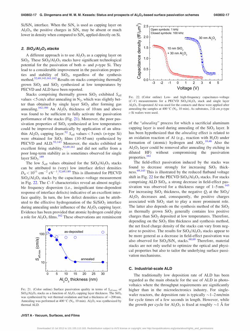
Si/SiNx interface. When the SiNx is used as capping layer on
Al2O3, the positive charges in SiNx may be absent or much
lower in density when compared to SiNx applied directly on Si.
2. SiO2/Al2O3 stacks
A different approach is to use Al2O3 as a capping layer on
SiO2. These SiO2/Al2O3 stacks have significant technological
potential for the passivation of both n- and p-type Si. They
lead to a considerable improvement in the passivation proper-
ties and stability of SiO2, regardless of the synthesis
method.52,69,143,161,162 Results on stacks comprising thermally
grown SiO2 and SiO2 synthesized at low temperatures by
PECVD and ALD have been reported.
Stacks comprising thermally grown SiO2 exhibited Seff
values <5 cm/s after annealing in N2, which was slightly bet-
ter than obtained by single layer SiO2 after forming gas
annealing.162,180 An Al2O3 thickness of 10 nm and above
was found to be sufficient to fully activate the passivation
performance of the stacks (Fig. 21). Moreover, the poor pas-
sivation properties of SiO2 synthesized at low temperatures
could be improved dramatically by application of an ultra-
thin Al2O3 capping layer.52 Seff values< 5 cm/s (n-type Si)
were obtained for SiO2 films (10–85 nm) synthesized by
PECVD and ALD.52,143 Moreover, the stacks exhibited an
excellent firing stability,52,69,161 and did not suffer from a
poor long-term stability as is sometimes observed for single
layer SiO2.189
The low Seff values obtained for the SiO2/Al2O3 stacks
can be attributed to (very) low interface defect densities
Dit< 1011 cm�2 eV�1.52,69,189 This is illustrated for PECVD
SiO2/Al2O3 stacks by the capacitance–voltage measurement
in Fig. 22. The C–V characteristics reveal an almost negligi-
ble frequency dispersion (i.e., insignificant time-dependent
response of interface defects) indicative of an excellent inter-
face quality. In turn, the low defect densities can be attrib-
uted to the effective hydrogenation of the Si/SiO2 interface
during annealing under influence of the Al2O3 capping layer.
Evidence has been provided that atomic hydrogen could play
a role for Al2O3 films.162 These observations are reminiscent
of the “alnealing” process for which a sacrificial aluminum
capping layer is used during annealing of the SiO2 layer. It
has been hypothesized that the alnealing effect is related to
an oxidation reaction of Al (e.g., reaction with H2O) under
formation of (atomic) hydrogen and AlOx.10,46 Also the
Al2O3 layer could be removed after annealing (by etching in
diluted HF) without compromising the passivation
properties.161
The field-effect passivation induced by the stacks was
found to decrease strongly for increasing SiO2 thick-
ness.69,143 This is illustrated by the reduced flatband voltage
shift in Fig. 22 for the PECVD SiO2/Al2O3 stacks. For stacks
comprising ALD SiO2, a strong decrease in field-effect pas-
sivation was observed for a thickness range of 1–5 nm.143
For increasing SiO2 thickness, the negative Qf at the SiO2/
Al2O3 decreases and, consequently, the positive charges
associated with SiO2 start to play a more prominent role.
The latter also depends on the synthesis method of the SiO2
as thermally grown SiO2 generally contains less positive
charges than SiO2 deposited at low temperatures. Therefore,
depending on the SiO2 film thickness and synthesis method,
the net fixed charge density of the stacks can vary from neg-
ative to positive. The results for SiO2/Al2O3 stacks appear to
be more general as a decrease in field-effect passivation was
also observed for SiO2/SiNx stacks.68,69 Therefore, material
stacks are not only useful to optimize the optical and physi-
cal properties but also to tailor the underlying surface passi-
vation mechanisms.
C. Industrial-scale ALD
The traditionally low deposition rate of ALD has been
regarded as the main obstacle for the use of ALD in photo-
voltaics where the throughput requirements are significantly
higher than in the microelectronics industry. For single-
wafer reactors, the deposition rate is typically �1–2 nm/min
for cycle times of a few seconds in length. However, while
the growth per cycle for Al2O3 is fixed at roughly �1 A for
0 5 10 15 20 25 30
10
100
Sef
f,max
(cm
/s)
Al2O3 thickness (nm)
as-deposited
annealed
FIG. 21. (Color online) Surface passivation quality in terms of Seff,max of
SiO2/Al2O3 stacks as a function of Al2O3 capping layer thickness. The SiO2
was synthesized by wet thermal oxidation and had a thickness of �200 nm.
Annealing was performed at 400 C (N2, 10 min). Al2O3 was synthesized by
thermal ALD.
-3 -2 -1 0 1 2 3 4 50.0
0.5
1.0
1.5
2.0
2.5
30 nm Al2O3
Cap
acita
nce
dens
ity (f
F/µm
2 )
Voltage (V)
10 nm SiO2
+ 30 nm Al2O3
Open symbols: 1 kHzClosed symbols: 100 kHz
FIG. 22. (Color online) Low- and high-frequency capacitance–voltage
(C–V) measurements for a PECVD SiO2/Al2O3 stack and single layer
Al2O3. Evaporated Al was used for the contacts and these were applied after
annealing the samples at 400 C (N2, 10 min). As substrates, 2 X cm p-type
c-Si wafers were used.
040802-17 G. Dingemans and W. M. M. Kessels: Status and prospects of Al2O3-based surface passivation schemes 040802-17
JVST A - Vacuum, Surfaces, and Films
Downloaded 10 Jul 2012 to 131.155.113.183. Redistribution subject to AVS license or copyright; see http://avspublications.org/jvsta/about/rights_and_permissions

all ALD equipment, the duration of the cycle and the number
of wafers that can be deposited simultaneously, and there-
with the deposition rate (i.e., thickness per unit of time per
wafer), can vary substantially. With the incentive to over-
come the throughput limitations of existing ALD Al2O3
methods, equipment manufacturers such as Beneq and ASM
have redesigned or adapted their ALD batch tools, which
were originally designed for the semiconductor industry, to
meet the throughput requirements of typically >3000 solar
cells/h. Moreover, spatial ALD equipment has recently been
developed specifically for the deposition of Al2O3 for PV
applications.21
The concept of spatial ALD was already described in
the original ALD patent of Suntola.190 More recently,
technology to enable atmospheric spatial ALD has been
explored by Levy et al.191 The difference between spatial
and temporal ALD pertains to the separation of the precur-
sor and oxidant steps (Fig. 23). In conventional temporal
ALD processes, such as used in batch reactors, the precur-
sor and oxidants are injected sequentially into the same re-
actor volume. In spatial ALD, the precursor and oxidants
are separated spatially in different zones of the reactor.
Two spatial ALD concepts have been commercialized—by
SoLayTec and by Levitech.192,193 Both concepts are quite
similar with the main difference being the transport of the
wafers (Fig. 23). The Levitech approach is based on an
inline reactor (the Levitrack) where transport is controlled
by an atmospheric gas bearing on which the wafer floats.
While the wafer moves through the reactor, it is sequen-
tially exposed to Al(CH3)3, N2, H2O, and again N2. The
precursor zones are repeated over the length of the track,
which also has a heating and cooling zone in the initial
and final part of the reactor. The system yields �1 nm
Al2O3 per 1 m system length in its current configuration.
In the SoLayTec reactor, the wafer moves back and forthunderneath TMA and H2O injection zones. Therefore, film
thickness is independent of system length. As is the case
in the Levitrack, wafer movement is fully controlled by
gas flows. In the SoLayTec concept, the deposition rate
depends on the number of injection slots integrated in the
injector head and the number of passages of the wafer per
second.
In spatial ALD, the cycle time is ultimately dictated by the
speed of the precursor reactions at the growth surface and not
by the purge steps that avoid parasitic CVD reactions between
precursors. Both spatial ALD reactors lead to significantly
higher deposition rates (e.g., 30–70 nm/min) than generally
obtained by temporal ALD (a few nm/min at most). Other
benefits of these reactors are that no vacuum pumps are
required as the reactors are operated under atmospheric pres-
sure conditions, and that, in the ideal case, only the wafer is
coated (either single-side or double-side depending on the re-
actor design) and not the reactor walls. In addition, there are
no moving equipment parts apart from the wafers. More
details on spatial ALD and the systems can be found in Refs.
20 and 21 and 194–198.
An important question to address is whether the scale-up
of the ALD processes compromises the passivation proper-
ties of Al2O3 films in comparison with single-wafer labora-
tory systems. Here, we focus on the passivation properties of
Al2O3 films that were deposited in an ASM ALD batch reac-
tor and in the inline ALD reactor from Levitech.
1. Batch ALD
The surface passivation properties of Al2O3 deposited in
the ASM ALD batch reactor were optimized for substrate
temperature and precursor dosing times. O3 was used as the
oxidant and the lifetime wafers were deposited at both sides
simultaneously. The wafers can also be placed back-to-back,
which results in single-side deposition of twice the amount
of wafers and, therefore, a higher wafer throughput. The
Al2O3 films afforded a low level of surface passivation in the
as-deposited state. This is similar to the results for plasma
FIG. 23. (Color online) (a) Schematic representation of atomic layer deposition processes for oxides where the precursor dose step and the oxidant are (i) sepa-
rated in time or (ii/iii) separated spatially. The precursor and oxidant are prevented from reacting with each other, either by purging the reactor or by their spa-
tial separation involving purge flows in between the precursor inlets. (b) Schematic of an ALD batch reactor. (c) Spatial ALD setup as commercialized by the
company Levitech, where the wafer moves through an inline reactor, see also (ii). Note that (iii) is the approach commercialized by the company SolayTec,
where the substrate moves back and forth between two reactor zones.
040802-18 G. Dingemans and W. M. M. Kessels: Status and prospects of Al2O3-based surface passivation schemes 040802-18
J. Vac. Sci. Technol. A, Vol. 30, No. 4, Jul/Aug 2012
Downloaded 10 Jul 2012 to 131.155.113.183. Redistribution subject to AVS license or copyright; see http://avspublications.org/jvsta/about/rights_and_permissions

ALD. The surface passivation was activated by annealing,
resulting in low Seff values< 6 cm/s for Al2O3 films with a
thickness of �15 nm for 2 X cm p-type Si wafers.107 This
high level of passivation after annealing can be explained by
a high fixed negative charge density of 3.4� 1012 cm�2 and
a low interface defect density Dit of �1� 1011 eV�1 cm�2
as determined by C–V measurements.107
2. Spatial ALD
The Al2O3 films deposited in the Levitrack afforded some
surface passivation in the as-deposited state with
Seff< 50 cm/s for a film thickness of �15 nm. This is in
agreement with results for thermal ALD with H2O in a lab
scale reactor (Fig. 14). After a standard anneal, the effective
lifetime increased significantly to seff ¼ 2.5 ms, resulting in
very low Seff< 6 cm/s [Fig. 24(a)].180 Reference samples de-
posited with plasma ALD Al2O3 in a single-wafer reactor
showed similar low Seff values. For annealed films, Seff
decreased with increasing film thickness and saturated for
thicknesses >�10 nm. Interestingly, after a subsequent firing
process in an industrial belt line furnace (T> 800 C), the
thickness dependence of the passivation disappeared. Ultra-
thin films of �5 nm yielded relatively low Seff values
<25 cm/s after firing. Regarding the field-effect passivation,
it was verified by corona charging experiments that the spa-
tial ALD Al2O3 films exhibited a high negative Qf of
(4 6 0.5)�1012 cm�2 after annealing [Fig. 24(b)].
The excellent passivation results for the spatial and batch
ALD Al2O3 processes are comparable to those obtained for
single-wafer reactors. This is also true for the Al2O3 films de-
posited in the spatial ALD tools of SoLayTec, which led to low
Seff values of <8 cm/s on low-resistivity p- and n-type Si.197,198
Therefore, no apparent compromised performance in terms of
resulting passivation quality was observed when going to
scaled-up ALD processes. To date, spatial and batch ALD
equipment has already been installed in pilot production lines
at a number of solar cell manufacturers and research institutes.
3. ALD or PECVD?
PECVD is a serious contender for the deposition of Al2O3
in the PV industry. Good surface passivation properties
(Seff< 10 cm/s, 1 X cm p-type Si), on par with ALD, have
been reported for Al2O3 synthesized by PECVD in an indus-
trial Roth & Rau reactor.124 A difference may be the refrac-
tive index of the PECVD deposited films, which is generally
somewhat lower (�1.60) than for ALD (�1.64).124,125 This
is indicative of a slightly lower film density.
The PECVD and the ALD processes both have strengths
and weaknesses. Hence, it is likely that there are opportunities
for both—and perhaps also other—deposition technologies
depending on specific demands and applications. When ultra-
thin Al2O3 films are required (<10 nm), the thickness control
and uniformity of ALD may provide key benefits over PECVD.
This will also be the case for concepts in which Al2O3 films are
required on both sides of the solar cell, and for more advanced
passivation schemes comprising stacks of ALD materials,
nanolaminates, or perhaps doped and mixed oxides. However,
when thick Al2O3 films are required, PECVD may be the pre-
ferred option. In the end, cost-of-ownership considerations
(such as operational costs, footprint, equipment down-time, pre-
cursor consumption, etc.) may be at least as important as the
purely technological specifications of the system.
D. Alternative precursors
1. Solar grade TMA
Cost-of-ownership for Al2O3 deposition technology could
be reduced when, instead of highly purified “semiconductor
grade” Al(CH3)3, a lower cost precursor can be used. The pre-
cursor costs are directly related to the number of purification
steps required during precursor synthesis. Possible impurities
that can be present in lower grade TMA include Ga, Zn, Cl
atoms. To assess the possible influence of the purity level on
the passivation properties of the Al2O3 films, Al(CH3)3 with
two different purities, i.e., semiconductor grade and solar
grade, were compared.180 For both thermal and plasma ALD,
no significant difference was observed between the two pre-
cursors in terms of resulting passivation performance. This
holds for both p- and n-type silicon. It can therefore be con-
cluded that the surface passivation is not compromised by the
higher impurity level of solar grade Al(CH3)3. This compati-
bility is crucial for large-scale production.
2. DMAI
As an alternative to Al(CH3)3, dimethylaluminium iso-
propoxide [AlMe2(OiPr)] can be used as Al precursor during
ALD. This novel precursor (in brief DMAI), commercialized
by Air Liquide, is not pyrophoric. DMAI is therefore safer to
handle and store than TMA. In the DMAI molecule, the Al
atom is bonded to an isopropoxide group and to two methyl
groups [Fig. 25(inset)]. DMAI can be used in combination
with O3, H2O, or an O2 plasma as coreactants. A saturated
process was developed for plasma and thermal ALD in our
OpAL reactor.199 Slightly longer dosing times (�100 ms)
were required for DMAI than for TMA, which can be
0 5 10 15 201
10
100
0 2 4 6 8
20
30
40
50
60(b)
Seff,m
ax (cm/s)as-deposited
annealedfiredplasma ALD ref.
Sef
f,max
(cm
/s)
Al2O3 film thickness (nm)
as-deposited
annealed
after firing
(a)
Qcorona (1012 cm-2)
FIG. 24. (Color online) Results obtained for the inline thermal ALD reactor
of Levitech. (a) Thickness dependence of the passivation performance of
Al2O3, for as-deposited films, after annealing (10 min) and after subsequent
firing at �850 C. The results are compared with plasma ALD reference
samples. (b) Corona charging graph for an 18 nm Al2O3 film after annealing.
A negative Qf of �4� 1012 cm�2 was obtained. Wafers with a resistivity of
�2 X cm (p-type) were used as substrates.
040802-19 G. Dingemans and W. M. M. Kessels: Status and prospects of Al2O3-based surface passivation schemes 040802-19
JVST A - Vacuum, Surfaces, and Films
Downloaded 10 Jul 2012 to 131.155.113.183. Redistribution subject to AVS license or copyright; see http://avspublications.org/jvsta/about/rights_and_permissions
attributed to a lower vapor pressure for DMAI (9 Torr at
66.5 C) than for TMA (9 Torr at 16.8 C). The plasma ALD
process yielded a growth rate of 0.9 A/cycle for Tdep ¼200 C, which is lower than the 1.2 A obtained when using
TMA in plasma ALD. In addition, the DMAI-Al2O3 films
exhibited a higher hydrogen content of �7 at. % and, conse-
quently, a lower mass density of �2.6 g/cm3 (Tdep ¼ 200 C)
compared to Al2O3 deposited from TMA. These differences
illustrate that a relatively small change to the precursor mol-
ecule can give rise to different growth and material
properties.
The surface passivation performance of the DMAI-Al2O3
films is displayed in Fig. 25, comparing results for n- and p-
type c-Si. Before annealing, the passivation performance
was very poor with Seff values of the order of 103 cm/s, as
expected for plasma ALD. After annealing, the effective life-
time is observed to improve significantly. Seff values <6 and
<3 cm/s were obtained for p- and n-type Si, respectively.
These values are quite comparable to those reported for
plasma ALD Al2O3 using Al(CH3)3.
VII. SOLAR CELLS FEATURING Al2O3
One key aspect of all high-efficiency solar cells is the incor-
poration of effective surface passivation schemes on the front
and/or rear side. Figure 26 illustrates a selection of solar cell
structures based on p-type and n-type Si base material. It is
evident that the number of process steps required for the fabri-
cation of the different cells varies widely. The industrial stand-
ard screen-printed p-type Si solar cell, which can be
manufactured in only eight process steps, exemplifies the sim-
plest device structure [Fig. 26(i)]. The energy conversion effi-
ciency of this type of solar cell can be increased by improving
the front side, e.g., by using a selective emitter and higher as-
pect ratio front contacts. However, to achieve a significant
increase in efficiency, it is necessary to also improve the rear
side by the implementation of a passivated rear with local
backsurface field (PERC-type solar cell). The PERC-type
design is compatible with high cell efficiencies,47,200 and is
currently being introduced in mass production. The adaptation
from the standard Al-BSF cell to a PERC cell requires the dep-
osition of a rear passivation film, local contact formation by,
for example, laser processing,201,202 but it also changes, for
example, the requirements for the optimal Si bulk resistiv-
ity9,203 and the composition of the metal pastes. Another route
to realize high efficiencies is the use of n-type Si base material.
The effective passivation of pþ emitters by Al2O3 has been an
important step forward for various types of n-type Si solar
cells. An advantage of using n-type Si is the high bulk lifetime,
which does not suffer from light-induced degradation by the
formation of boron-oxygen complexes as is the case for Czo-
chralski (Cz) p-type Si. This is one of the reasons why cells
based on n-type Cz Si have a higher efficiency potential than
those using Cz p-type Si.9 However, for n-type cells, an nþ
BSF [or front surface field (nþ FSF)] cannot be simply formed
FIG. 25. (Color online) Injection-level-dependent effective lifetime for
Al2O3 films synthesized by plasma ALD using DMAI as precursor for Al.
Annealing was performed at 400 C (10 min, N2). Data for n- (3.5 X cm)
and p-type (2 X cm) Si is shown (Ref. 199). Inset shows precursor drawings,
comparing TMA and DMAI.
FIG. 26. (Color online) Various solar cell concepts based on p- and n-type Si wafers. (i) Full Al-BSF; (ii) passivated emitter and rear (PERC) cell; (iii) back-
contacted emitter wrap through (BC EWT) cell; (iv), (v) passivated emitter and rear totally diffused (PERT) cell; (vi) passivated emitter and rear locally dif-
fused (PERL) cell; (vii) backjunction Al alloyed rear emitter (“BJ-Alpþ”) cell; (viii) backjunction PERT cell; (ix) bifacial cell; (x) interdigitated
backcontacted backjunction (IBC BJ) cell; (xi) backcontacted emitter wrap through (BC EWT) cell; (xii) heterojunction (HJ) cell.
040802-20 G. Dingemans and W. M. M. Kessels: Status and prospects of Al2O3-based surface passivation schemes 040802-20
J. Vac. Sci. Technol. A, Vol. 30, No. 4, Jul/Aug 2012
Downloaded 10 Jul 2012 to 131.155.113.183. Redistribution subject to AVS license or copyright; see http://avspublications.org/jvsta/about/rights_and_permissions
during the metallization process similar to the formation of the
Al-BSF for p-type cells and therefore requires additional pro-
cess steps. On the other hand, screen printing can be employed
to create an Al-pþ emitter at the rear side[Fig. 26 (vii)]. It is
important to note, however, that elaborate cleaning steps are
required to remove the Al and passivate the emitter. Obviously
passivation of the emitter is more straightforward when using
boron diffusion or ion implementation processes.204
Al2O3-based passivation schemes have been employed
for various types of solar cells listed in Fig. 26. An overview
of important results is presented in Table II. Note that not all
efforts could be included, given the accelerating activity in
the field.
A. p-type Si cells
The first p-type PERC solar cell featuring Al2O3 surface pas-
sivation was reported in 2008 by Schmidt et al.205 It was dem-
onstrated on cell level that the passivation performance of
Al2O3 can be on par or superior to alnealed thermally grown
SiO2. An effective surface recombination velocity of �70 cm/s
was deduced from the internal quantum efficiency measure-
ments for Al2O3 with a PECVD SiOx capping layer and local
rear contacts. The SiOx capping films can be applied on top of
the thin Al2O3 films to improve the rear reflection properties.
Efficiencies of 20%–20.6% were reported, which were later
increased up to 21.4% (Jsc = 40.7 mA/cm2, Voc = 664 mV,
FF = 79.4%) in a follow-up experiment.182 As expected, the
Al2O3-passivated PERC cells did not suffer from parasitic
shunting (by the formation of an inversion layer), as can be the
case when SiNx is applied on the rear. By direct comparison, it
was furthermore concluded that Al2O3 synthesized by sputtering
led to a lower Voc and g compared to ALD Al2O3 films, which
is consistent with the differences in passivation quality as
deduced from effective lifetime measurements.182 Very similar
efficiencies of up to 21.5% have been reported for PERC cells
by Saint-Cast et al.188 The passivation by PECVD or plasma
ALD Al2O3 led to similar solar cell performance. Moreover, the
rear reflection properties for single layer Al2O3 with a thickness
of �100 nm were equivalent to those of SiO2 or Al2O3/SiOx
stacks. The high open-circuit voltages >675 mV clearly demon-
strate the excellent rear surface passivation properties of the
Al2O3 films.188 The front side of the PERC cells in Refs. 188
and 205 exhibited high-efficiency nþ emitters of 100 and 120
X/sq, respectively. In Ref. 205, the emitter surface was very
lightly oxidized (“tunnel oxidation,” leading to �1.5 nm SiOx)
to improve the front side contact resistance and therewith the
fill-factor (FF) of the cells. Zielke et al. have recently demon-
strated that a few ALD cycles of Al2O3 on top the nþ emitter
also had a positive impact on the cell efficiency and reproduci-
bility.206 However, when more than two ALD cycles were
employed, a decrease in FF and g was observed, which the
authors ascribed to a decrease in tunneling probability. A similar
front and rear passivation scheme was used by Petermann et al.for thin 43 lm epitaxial Si layer solar cells in combination with
the porous Si layer transfer process.207 Partially due to the
improved surface passivation, they were able to improve the
efficiency of this type of solar cells from 16.9% to 19.1%.
It is important to note that the laboratory-type PERC cells dis-
cussed before were based on high-quality FZ Si (B-doped,
0.5 X cm, �4 cm2) with an evaporated Al backcontact. Either
TABLE II. Selection of solar cell results with implemented Al2O3-based surface passivation schemes. The “solar cell types” in the first column refer to Fig.
26.
Solar cell type Passivation layer(s) Cell efficiency (%) Additional details References
p-PERC (ii) (Rear) ALD Al2O3þSiOx 21.4 Al evaporated contacts, 0.5 X cm FZ, 4 cm2 182, 205
(Rear) sputtered Al2O3þSiOx 20.1 182
p-PERC (ii) (Rear) ALD Al2O3þSiOx 21.3 Al rear, plated front contacts, 188
(Rear) PECVD Al2O3þSiOx 21.5 0.5 X cm FZ, 4 cm2
p-PERC (ii) (Front) few ALD cycles Al2O3þSiNx ARC;
(rear) Al2O3/SiNx stack
21.7 Al evaporated contacts, 0.5 X cm FZ, 4 cm2 206
19.1 43 lm thick, B-doped epitaxial Si, 0.5 X cm FZ, 4 cm2 207
p-PERC (ii) (Rear) Al2O3/SiNx stack 18.6 Screen-printed, 3 X cm Cz, 125� 125 mm 208
p-PERC (ii) (Rear) Al2O3/SiNx stack 19.0 Screen-printed, 2–3 X cm Cz, 125� 125 mm 184
p-PERC (ii) (Rear) Al2O3/SiOx/SiNx stack 19.1 Screen-printed, 1 X cm Cz, 148.25 cm2 209
n-PERT (iv) (Front) Al2O3/ SiNx 20.8 (FZ) Full metallization of nþ diffused rear side, 213
19.4 (Cz) 90 X/sq pþ, 1 X cm FZ, 4 cm2
n-PERL (vi) (Front) Al2O3/SiNx stack
(Rear) thermal SiO2 23.9
Local diffused nþ BSF,
140 X/sq pþ, 1 X cm FZ, 4 cm2 9, 19
n-PERL (vi) (Front) Al2O3/SiNx stack 22.4 Local nþ BSF (PassDop, Laser doping), 212
(Rear) a-Si:C 1 X cm FZ, 4 cm2
n-IBC (x) (Rear) Al2O3 19.0 Al-pþ/nþ (rear side), 220
(Front) SiNx 2 X cm Cz, 4 cm2
EWT (xi) (Front/rear pþ) Al2O3/SiNx 21.6 1.5 X cm Cz, 4 cm2 221
(Rear nþ BSF) thermal SiO2þ Al2O3/SiNx
040802-21 G. Dingemans and W. M. M. Kessels: Status and prospects of Al2O3-based surface passivation schemes 040802-21
JVST A - Vacuum, Surfaces, and Films
Downloaded 10 Jul 2012 to 131.155.113.183. Redistribution subject to AVS license or copyright; see http://avspublications.org/jvsta/about/rights_and_permissions
photolithography-based processes were used to create openings
in the rear surface passivation scheme,205 or laser-fired-contacts
(LFCs) were implemented.188
Results on industrially feasible PERC cells, based on Cz-Si
and screen-printed metallization, have also been reported
(Table II). For these type of cells, a stack of Al2O3/a-SiNx:H
is used on the rear, instead of single layer Al2O3. This is
chiefly related to the high chemical stability of N-rich SiNx
when covered by metal paste. Lauermann et al. reported a
�0.7% higher (absolute) efficiency for PERC cells (18.6%)
than for Al-BSF reference cells.208 The combination of
increased surface passivation performance and enhanced rear
reflection led to an increase of Jsc by 1.5 mA/cm2 compared
to the references. These results demonstrate on a device level
that the Al2O3/SiNx passivation scheme is sufficiently firing
stable. Gatz et al. reported an energy conversion efficiency of
19.0% for large area Cz Si solar cells passivated by an Al2O3/
SiNx stack.184 As expected, the Jsc (38.9 mA/cm2) and Voc
(652 mV) were significantly higher than for the Al-BSF refer-
ence (g ¼ 18.6%, Jsc ¼ 37 mA/cm2, Voc ¼ 636 mV). Very
recently, Vermang et al. reported an efficiency of 19.1% for a
PERC cell with a triple-layer Al2O3/SiOx/SiNx stack on the
rear.209 Taken together, the PERC cells exhibited significantly
lower FF values [e.g., 77.2% (Ref. 208) and 75.1% (Ref.
184)] than were obtained for the Al-BSF references (79.5%
and 78.7%, respectively). An enhanced series resistance asso-
ciated with the local (line or point) contacts is responsible for
this difference. For PERC cells, the pitch and local contact
size are critical parameters for optimizing the rear side, which
involves a trade-off between a low contact resistance (narrow
pitch and large contacts) and low surface recombination
velocities (wide pitch and small contacts). Ongoing optimiza-
tion of metal pastes for local contacts will contribute to further
reductions in contact resistance. Apart from laser ablation (or
etching) of the dielectric prior to metallization, another indus-
trially feasible option is to use LFCs at the rear side where
structuring is done after the application of the metal paste.201
An alternative rear side metallization process based on an
open grid is used for the so-called PASHA cell (Passivated on
all sides H-pattern), compare Fig. 26 (ix).210 Although the ef-
ficiency potential for these cells is somewhat lower than for
PERC cells, the fabrication is simpler as the contacts are fired
through the dielectric layer forming an effective BSF. A cap-
ping layer on Al2O3 is not necessary.
Apart from PERC cells based on Cz-Si, excellent results
were reported recently by Q-Cells for industrially manufac-
tured multicrystalline Si (mc-Si) cells with improved front
and rear side. Using a rear surface passivation stack (materi-
als undisclosed) and LFCs, Engelhart and co-workers
demonstrated record efficiencies of up to 19.5% (mc-Si)
and 20.2% (Cz-Si).203,211 The authors estimated that the
improvement in Jsc due to enhanced rear reflection (DJsc � 1
mA/cm2) was almost as important as the reduction in elec-
tronic rear side recombination (DJsc � 1.2 mA/cm2) for the
mc-Si cells (Jsc ¼ 38.9 mA/cm2, Voc ¼ 652 mV, FF ¼ 76.7%).
These solar cell results demonstrate clearly that rear side sur-
face passivation is not only useful for monocrystalline Si cells
but has also significant potential for cells based on lower
quality Si substrates, which was previously unexpected. More-
over, these developments suggest that the performance gap
between industrially produced Cz-Si cells and cheaper mc-Si
cells can be reduced by the implementation of new technolo-
gies. Finally, it is important to point out that a fair comparison
between various surface passivation schemes should also
address the solar cell performance under low-illumination
conditions.211
B. n-type Si cells
Al2O3-based passivation was first tested for n-type Si solar
cells in a PERL cell design. An Al2O3/SiNx stack was used on
the front side boron emitter (�140 X/sq).19 Hoex et al. demon-
strated that Al2O3-passivated boron emitters with comparable
sheet resistance lead to ultralow J0 of �10 fA/cm2.137 For the
PERL cell, Benick et al. reported record efficiencies of, at that
time, 23.2% (or 23.4% after adjustment of the AM1.5 spec-
trum).19 In subsequent work, the efficiency was even improved
further to 23.9%.9 Internal quantum efficiencies of approxi-
mately 100% were obtained for the front side, in combination
with Voc values >700 mV. These results underline the passiva-
tion properties of Al2O3 for highly doped p-type surfaces on a
device level. The PERL cell, featuring local nþ BSFs fabricated
using photolithography processes, presents a complex cell con-
cept involving many different process steps. To simplify the
formation of the nþ BSF, a novel process was developed at
Fraunhofer ISE where a phosphorous containing passivation
layer (called PassDop) is locally opened by a laser under the si-
multaneous diffusion of P atoms into Si. Using this process,
promising efficiencies of 22.4% have already been demon-
strated.212 A next step toward industrial feasibility is the use of
screen-printed metallization.
Another approach, which is compatible with industrial proc-
essing, consists of a full-area nþ diffusion. [Fig. 26 (iv)] . Richter
et al. demonstrated efficiencies of 20.8% for this concept using
an Al2O3/SiNx stack on the front side pþ emitter (90 X/sq) in
combination with screenprinting technology.213 The p–n junction
can also be formed at the rear side by the formation of an Al-pþ
emitter and efficiencies up to 19.8% have been reported.214 It is
evident that both cells are limited by the properties of the rear
side, which does not comprise dielectric passivation. Therefore,
to further improve the energy conversion efficiency, a passivated
rear with local contacts can be implemented similar to p-type
PERC cells. In a preliminary study, SiNx and SiONx/SiNx stacks
have been evaluated for the passivation of the rear nþ BSF.215 In
combination with a stack comprising 0.5 nm Al2O3 and 70 nm
SiNx on the front side, a significantly enhanced Voc of 671 mV
was obtained, which represented an increase of �15 mV com-
pared to the cell with fully metalized BSF. At Q-Cells, the poten-
tial of concept (viii) was evaluated (Fig. 26). As the p–n junction
is moved to the rear side, the front side can be manufactured
similarly to conventional industrial p-type cells. First results al-
ready demonstrated a promising efficiency of 20.2% for large
area Cz cells using industrially feasible techniques (passivation
materials not disclosed).216
In addition to the PERL and PERT cells, various other n-
type cell designs have the potential of high efficiencies and can
040802-22 G. Dingemans and W. M. M. Kessels: Status and prospects of Al2O3-based surface passivation schemes 040802-22
J. Vac. Sci. Technol. A, Vol. 30, No. 4, Jul/Aug 2012
Downloaded 10 Jul 2012 to 131.155.113.183. Redistribution subject to AVS license or copyright; see http://avspublications.org/jvsta/about/rights_and_permissions

therewith exploit the benefits of n-type Si over p-type Si base
material. Bifacial cells [Fig. 26 (ix)] have attracted considerable
attention due to the simplicity of the rear side, which does not
require any structuring or local opening of the passivation layer.
Efficiencies of 19.5% have been reported for industrially pro-
duced cells by Yingli in collaboration with Energy Center
Netherlands.217 Although promising, to our knowledge no
results have been reported for n-type bifacial cells with Al2O3
passivation as yet. Another concept compatible with very high
efficiencies is the so-called interdigitated backcontacted (IBC)
cell design, which has been commercialized by Sunpower.
Exceptionally high efficiencies up to 24.2% have been real-
ized.84 Low recombination on the front side—obtained by
effective surface passivation and/or the implementation of an
FSF—and in the Si bulk are crucial as the minority carriers
generated near the front side have to diffuse to the rear p–njunction. At the rear side, a passivation scheme compatible
with both nþ- and pþ-type Si is required. Moreover, depending
on cell design, the passivation scheme needs to ensure excellent
electrical insulation as the oversized metal contacts (of the nþ
BSF) need to be isolated from the emitter underneath. Gong
et al. reported that higher implied Voc values were obtained
when using Al2O3 instead of SiOx/SiNx on the Al-pþ emitters,
but this was not yet corroborated on the solar cell level.218
Reichel et al. have reported efficiencies up to 23% for IBC
cells, but no details were given concerning the rear side passi-
vation.219 IBC cells with a screen-printed Al-pþ emitter have
been reported by Bock et al. For these cells with Al2O3 passiva-
tion on the rear side, efficiencies of 19% were obtained with
significant room for improvement up to 21.3%, as suggested by
device simulations.220 Another backcontacted cell concept is
the so-called emitter wrap through (EWT) cell. In this cell con-
cept, the requirements on the bulk lifetime and front side
recombination are less strict than in the IBC concept. There-
fore, a separate diffusion for the front side is not necessary for
the EWT cells. Kiefer et al. reported a cell efficiency of 21.6%
for EWT cells using Al2O3/SiNx passivation on the front and
rear side pþ emitter.221 Low J0,e of 60 and 35 fA/cm2 were
reported for the textured and planar pþ emitter (�50 X/sq)
surfaces. For the nþ BSF, the Al2O3/SiNx layers were deposited
on top of a thermally grown SiO2 layer. Note that Sun et al.employed such an SiO2/Al2O3 stack at the rear of p-type
PERC cells and reported excellent passivation properties and
g ¼ 20.1%.222 The SiO2/Al2O3 stack system leads to a high
level of chemical passivation (Sec. VI B). Moreover, the
absence of significant negative fixed charge density in the
SiO2/Al2O3 is expected to be beneficial for the passivation of
nþ surfaces.
Finally, heterojunction (HJ) cells critically rely on an
excellent level of surface passivation, typically realized by
using undoped a-Si:H thin films below the p- and n-doped a-
Si:H films [Fig. 26 (xii)]. The latter concept is used in the
successful Heterojunction with Intrinsic Thin layer cells
commercialized by Sanyo.11,84 Note that HJ technology can
also be combined with the IBC concept for realizing high
Voc and Jsc.81 It is expected that the passivation properties of
Al2O3 films can be exploited for HJ cells using innovative
approaches and cell designs. For example, Al2O3 could be
applied on a front side (diffused) pþ emitter for cells with an
nþ heterojunction at the rear side.9
VIII. CONCLUDING REMARKS
In this article the fast-growing activities relating to Al2O3
thin films applied for the passivation of Si surfaces since
2006 have been reviewed. The appearance of Al2O3 as a
very effective passivation material was not anticipated in the
field, where surface passivation schemes had primarily been
based on Si-containing films (e.g., SiO2, a-SiNx, and a-
Si:H). Compared to these other materials, a distinguishing
characteristic of the Al2O3 films is field-effect passivation
induced by negative fixed charges. Nonetheless, the very
low defect densities (Dit� 1011 eV�1 cm�2) induced by the
films are also essential for the low surface recombination
velocities that have been reported for p, pþ, and n-type Si.
Depending on sheet resistance, Al2O3 may even contribute
to sufficiently low emitter saturation current densities for nþ
Si, although SiO2/Al2O3 stacks without negative charges are
likely preferable.
Atomic layer deposition is also novel in the field of c-Si
photovoltaics. Because of its precise thickness control, ALD
is ideally suited for engineering the Si surface and tailoring
the properties of nanolayer surface passivation schemes. For
example, ultrathin SiO2 interlayers have been used to control
the fixed charge density associated with Al2O3. In addition,
the application of just a few ALD Al2O3 cycles, prior to
a-SiNx deposition, was demonstrated to be already sufficient
to improve the passivation properties of pþ emitters. Other
enticing possibilities for the future may include the use of
ALD for ultrathin pinhole-free inversion, barrier and tunnel-
ing layers, selectively doped films, and stacks in combina-
tion with transparent conductive oxides. This may contribute
to developments regarding novel low-recombination contact
and metallization schemes.
The use of ALD is no longer limited to ultrathin films of
only a few nanometers. With the availability—and further
development—of spatial ALD and large-scale batch reac-
tors, ALD may soon be a technologically and cost-effective
deposition process for the PV industry. The industry at large
has been relying on the successful screen-printed Al-BSF
technology for the last few decades, but it is expected that
the PERC-type solar cells featuring dielectric rear side passi-
vation will become a prominent technology in the next few
years. Subsequently, and partially concurrently, higher effi-
ciency n-type Si cells featuring passivation on the front and
rear sides will play an increasingly important role. It has
been demonstrated that Al2O3, deposited either by ALD or
PECVD, and in combination with an a-SiNx:H capping
layer, provides a metallization-stable solution for both p-
and n-type Si cells. Nonetheless, the integration of the
(novel) technologies (i.e., cleaning, deposition, contacting
methods) in industrial process flows can still pose chal-
lenges. In addition, methods to monitor the passivation qual-
ity during manufacturing have to be developed. Appropriate
tests (e.g., accelerated aging) to determine the long-term
040802-23 G. Dingemans and W. M. M. Kessels: Status and prospects of Al2O3-based surface passivation schemes 040802-23
JVST A - Vacuum, Surfaces, and Films
Downloaded 10 Jul 2012 to 131.155.113.183. Redistribution subject to AVS license or copyright; see http://avspublications.org/jvsta/about/rights_and_permissions
field performance of surface passivation films are also not
available yet.
In the broader field of photovoltaics, surface passivation
schemes based on ALD Al2O3 may be a natural choice for
future developments regarding nano- and microwire solar
cells223–225 and other next-generation concepts that require
ultrathin conformal films.226 However, given the urgency for
the large-scale adoption of sustainable energy sources, we
hope that the technology described in this paper will contrib-
ute significantly to improving the conversion efficiency of
industrial solar cells and further reducing the price of solar
electricity on the short term.
ACKNOWLEDGMENTS
The authors gratefully acknowledge M. C. M. van de San-
den, N. M. Terlinden, M. M. Mandoc, S. E. Potts, J. A. van
Delft, C. A. A. van Helvoirt and W. Keuning (TU/e), E. H.
A. Granneman and P. Vermont (Levitech), D. Pierreux
(ASM), S. Bordihn and P. Engelhart (Q-Cells), J. Hilfiker
(J.A. Woollam Co.), and Ch. Lachaud and A. Madec (Air
Liquide) for their valuable contributions to this work. M.
Fanciulli (MDM Italy) is kindly acknowledged for the
EDMR measurements.
1J. H. Zhao, A. H. Wang, and M. A. Green, Prog. Photovoltaics 7, 471
(1999).2M. A. Green, Prog. Photovoltaics 17, 183 (2009).3T. Tiedje, E. Yablonovitch, G. D. Cody, and B. G. Brooks, IEEE Trans.
Electron Devices 31, 711 (1984).4M. A. Green, IEEE Trans. Electron Devices 31, 671 (1984).5M. J. Kerr, A. Cuevas, and P. Campbell, Prog. Photovoltaics 11, 97
(2003).6M. A. Green, Silicon Solar Cells: Advanced Principles and Practice(Bridge Printery, Sydney, Australia, 1995).
7W. Shockley and H. J. Queisser, J. Appl. Phys. 32, 510 (1961).8R. M. Swanson, Proceedings of the 31st IEEE Photovoltaic SpecialistsConference, Lake Buena Vista, FL, 3–7 January 2005 (IEEE, New York,
2005).9S. W. Glunz et al., Proceedings of the 35th IEEE Photovoltaic SpecialistsConference, Honolulu, HI, 20–25 June 2010 (IEEE, New York, 2010).
10A. G. Aberle, Prog. Photovoltaics 8, 473 (2000).11Y. Tsunomura, T. Yoshimine, M. Taguchi, T. Baba, T. Kinoshita, H.
Kanno, H. Sakata, E. Maruyama, and M. Tanaka, Sol. Energy Mater. Sol.
Cells 93, 670 (2009).12R. Hezel and K. Jaeger, J. Electrochem. Soc. 136, 518 (1989).13G. Agostinelli, P. Vitanov, Z. Alexieva, A. Harizanova, H. F. W. Dekkers,
S. De Wolf, and G. Beaucarne, Proceedings of the 19th European Photo-voltaic Solar Energy Conference, Paris, 7–11 June 2004 (unpublished).
14B. Hoex, S. B. S. Heil, E. Langereis, M. C. M. van de Sanden, and W. M.
M. Kessels, Appl. Phys. Lett. 89, 042112 (2006).15G. Agostinelli, A. Delabie, P. Vitanov, Z. Alexieva, H. F. W. Dekkers, S. De
Wolf, and G. Beaucarne, Sol. Energy Mater. Sol. Cells 90, 3438 (2006).16B. Hoex, J. Schmidt, P. Pohl, M. C. M. van de Sanden, and W. M. M.
Kessels, J. Appl. Phys 104, 044903 (2008).17B. Hoex, J. J. H. Gielis, M. C. M. van de Sanden, and W. M. M. Kessels,
J. Appl. Phys. 104, 113703 (2008).18M. Hofmann, S. Janz, C. Schmidt, S. Kambor, D. Suwito, N. Kohn, J.
Rentsch, R. Preu, and S. W. Glunz, Sol. Energy Mater. Sol. Cells 93,
1074 (2009).19J. Benick, B. Hoex, M. C. M. van de Sanden, W. M. M. Kessels, O.
Schultz, and S. W. Glunz, Appl. Phys. Lett. 92, 253504 (2008).20W. M. M. Kessels and M. Putkonen, MRS Bull. 36, 907 (2011).21P. Poodt, D. C. Cameron, E. Dickey, S. M. George, V. Kuznetsov, G. N.
Parsons, F. Roozeboom, G. Sundaram, and A. Vermeer, J. Vac. Sci.
Technol. A 30, 010802 (2012).
22W. Shockley and W. T. J. Read, Phys. Rev. 87, 835 (1952).23R. N. Hall, Phys. Rev. 87, 387 (1952).24S. Rein, Lifetime Spectroscopy (Springer, Berlin, 2004).25A. G. Aberle, Crystalline Silicon Solar Cells: Advanced Surface Passiva-
tion and Analysis (University of New South Wales, Sydney, Australia,
1999).26R. B. M. Girisch, R. P. Mertens, and R. F. de Keersmaecker, IEEE Trans.
Electron Devices 25, 203 (1988).27A. G. Aberle, S. Glunz, and W. Warta, Sol. Energy Mater. Sol. Cells 29,
175 (1993).28S. W. Glunz, D. Biro, S. Rein, and W. Warta, J. Appl. Phys. 86, 683 (1999).29S. Olibet, E. Vallat-Sauvain, and C. Ballif, Phys. Rev. B 76, 035326
(2007).30A. B. Sproul, M. A. Green, A. W. Stephens, J. Appl. Phys. 72, 4161 (1992).31D. Macdonald and A. Cuevas, Sol. Energy 76, 255 (2004).32R. A. Sinton and A. Cuevas, Appl. Phys. Lett. 69, 2510 (1996).33H. Nagel, C. Berge, and A. G. Aberle, J. Appl. Phys. 86, 6218 (1999).34G. Coletti, R. Kvande, V. D. Mihailetchi, L. J. Geerlings, L. Arnberg, and
E. J. Vrelid, J. Appl. Phys. 104, 104913 (2008).35S. W. Glunz, S. Rein, J. Y. Lee, and W. Warta, J. Appl. Phys. 90, 2397
(2001).36J. Schmidt and K. Bothe, Phys. Rev. B 69, 024107 (2004).37D. Macdonald, F. Rougieux, A. Cuevas, B. Lim, J. Schmidt, M. Di Saba-
tino, and L. Geerlings, J. Appl. Phys. 105, 093704 (2009).38B. Lim, V. V. Voronkov, R. Falster, K. Bothe, and J. Schmidt, Appl.
Phys. Lett. 98, 162104 (2011).39M. J. Kerr and A. Cuevas, J. Appl. Phys. 91, 2473 (2002).40J. Benick, A. Richter, M. Hermle, and S. W. Glunz, Phys. Status Solidi
(RRL) 3, 233 (2009).41A. Stesmans and V. V. Afanas’ev, Appl. Phys. Lett. 80, 1957 (2002).42A. G. Aberle, S. Glunz, and W. Warta, J. Appl. Phys. 71, 4422 (1992).43M. L. Green, E. P. Gusev, R. Degraeve, and E. L. Garfunkel, J. Appl.
Phys. 90, 2057 (2001).44O. Schultz, A. Mette, M. Hermle, and S. W. Glunz, Prog. Photovoltaics
16, 317 (2008).45J. Benick, K. Zimmermann, J. Spiegelman, M. Hermle, and S. W. Glunz,
Prog. Photovoltaics 19, 361 (2011).46M. L. Reed and J. D. Plummer, J. Appl. Phys. 63, 5776 (1988).47A. W. Blakers, A. Wang, A. M. Milne, J. Zhao, and M. A. Green, Appl.
Phys. Lett. 55, 1363 (1989).48M. J. Kerr and A. Cuevas, Semicond. Sci. Technol. 17, 35 (2002).49S. Mack, A. Wolf, A. Walczak, B. Thaidigsmann, E. Allan Wotke, J. J.
Spiegelman, R. Preu, and D. Biro, Sol. Energy Mater. Sol. Cells 95, 2570
(2011).50W. D. Eades and R. M. Swanson, J. Appl. Phys. 58, 4267 (1985).51B. Hoex, F. J. J. Peeters, M. Creatore, M. A. Blauw, W. M. M. Kessels,
and M. C. M. van de Sanden, J. Vac. Sci. Technol. A 24, 1823 (2006).52G. Dingemans, M. C. M. van de Sanden, and W. M. M. Kessels, Phys.
Status Solidi (RRL) 5, 22 (2011).53V. D. Mihailetchi, Y. Komatsu, and L. J. Geerligs, Appl. Phys. Lett. 92,
063510 (2008).54S. Bordihn, P. Engelhart, V. Mertens, G. Kesser, D. Kohn, G. Dingemans,
M. M. Mandoc, J. W. Muller, and W. M. M. Kessels, Energy Procedia 8,
654 (2011).55C. Leguijt et al., Sol. Energy Mater. Sol. Cells 40, 297 (1996).56J. Schmidt and A. Cuevas, J. Appl. Phys. 85, 3626 (1999).57M. J. Kerr and A. Cuevas, Semicond. Sci. Technol. 17, 166 (2002).58S. de Wolf, G. Agostinelli, G. Beaucarne, and P. Vitanov, J. Appl. Phys.
97, 063303 (2005).59A. G. Aberle and R. Hezel, Prog. Photovoltaics 5, 29 (1997).60B. Hoex, A. J. M. van Erven, R. C. M. Bosch, W. T. M. Stals, M. D.
Bijker, P. J. van den Oever, W. M. M. Kessels, and M. C. M. van de San-
den, Prog. Photovoltaics 13, 705 (2005).61J. Hong, W. M. M. Kessels, W. J. Soppe, W. W. Weeber, W. M. Arnold-
bik, and M. C. M. van de Sanden, J. Vac. Sci. Technol. B 21, 2123 (2003).62F. Duerinckx and J. Szlufcik, Sol. Energy Mater. Sol. Cells 72, 231
(2002).63M. I. Bertoni et al., Prog. Photovoltaics 19, 187 (2010).64W. L. Warren, J. Kanicki, J. Robertson, E. H. Poindexter, and P. J.
McWhorter, J. Appl. Phys. 74, 4034 (1993).65S. E. Curry, P. M. Lenahan, D. T. Krick, J. Kanicki, and C. T. Kirk, Appl.
Phys. Lett. 56, 1359 (1990).66H. Mackel and R. Ludemann, J. Appl. Phys. 92, 2602 (2002).
040802-24 G. Dingemans and W. M. M. Kessels: Status and prospects of Al2O3-based surface passivation schemes 040802-24
J. Vac. Sci. Technol. A, Vol. 30, No. 4, Jul/Aug 2012
Downloaded 10 Jul 2012 to 131.155.113.183. Redistribution subject to AVS license or copyright; see http://avspublications.org/jvsta/about/rights_and_permissions

67S. Dauwe, L. Mittelstadt, A. Metz, and R. Hezel, Prog. Photovoltaics 10,
271 (2002).68G. Dingemans, M. M. Mandoc, S. Bordihn, M. C. M. van de Sanden, and
W. M. M. Kessels, Appl. Phys. Lett. 98, 222102 (2011).69S. Mack, A. Wolf, C. Brosinsky, S. Schmeisser, A. Kimmerle, P.
Saint-Cast, M. Hofmann, and D. Biro, IEEE J. Photovoltaics 1, 135
(2011).70M. Schaper, J. Schmidt, H. Plagwitz, and R. Brendel, Prog. Photovoltaics
13, 381 (2005).71S. Gatz, H. Plagwitz, P. P. Altermatt, B. Terheiden, and R. Brendel,
Appl. Phys. Lett. 93, 173502 (2008).72C. Leendertz, N. Mingirulli, T. F. Schulze, J. P. Kleider, B. Rech, and L.
Korte, Appl. Phys. Lett. 98, 202108 (2011).73T. F. Schulze, H. N. Beushausen, C. Leendertz, A. Dobrich, B. Rech, and
L. Korte, Appl. Phys. Lett. 96, 25102 (2010).74S. de Wolf, B. Demaurex, A. Descoeudres, and C. Ballif, Phys. Rev. B
83, 233301 (2011).75A. Illiberi, M. Creatore, W. M. M. Kessels, and M. C. M. van de Sanden,
Phys. Status Solidi (RRL) 4, 206 (2010).76A. Shah, P. Torres, R. Tscharner, N. Wyrsch, and H. Keppner, Science
285, 692 (1999).77R. W. Collins, A. S. Ferlauto, G. M. Ferreira, C. Chen, J. Koh, R. J.
Koval, Y. Lee, J. M. Pearce, and C. R. Wronski, Sol. Energy Mater. Sol.
Cells 78, 143 (2003).78A. H. M. Smets, W. M. M. Kessels, and M. C. M. van de Sanden, Appl.
Phys. Lett. 82, 1547 (2003).79M. N. van den Donker, B. Rech, W. M. M. Kessels, and M. C. M. van de
Sanden, New J. Phys. 9, 280 (2006).80G. Dingemans, M. N. van den Donker, D. Hrunski, A. Gordijn, W. M. M.
Kessels, and M. C. M. van de Sanden, Appl. Phys. Lett. 93, 111914 (2008).81N. Mingirulli et al., Status Solidi (RRL) 5, 159 (2011).82S. Martın de Nicola, D. Munoz, A. S. Ozanne, N. Nguyen, and P. J.
Ribeyron, Energy Procedia 8, 226 (2011).83D. L. Batzner et al., Energy Procedia 8, 153 (2011).84M. A. Green, K. Emery, Y. Hishikawa, W. Warta, and E. D. Dunlop,
Prog. Photovoltaics 20, 12 (2012).85R. Santbergen and R. J. C. van Zolingen, Sol. Energy Mater. Sol. Cells
92, 432 (2008).86T. Fellmeth, S. Mack, J. Bartsch, D. Erath, U. Jager, R. Preu, F. Clement,
and D. Biro, IEEE Electron Device Lett. 32, 1101 (2011).87J.-H. Lai, A. Upadhyaya, R. Ramanathan, A. Das, K. Tate, V. Upadhyaya,
A. Kapoor, C.-W. Chen, and A. Rohatgi, IEEE J. Photovoltaics 1, 16 (2011).88A. Wolf, D. Biro, J. Nekarda, S. Stumpp, A. Kimmerle, S. Mack, and R.
Preu, J. Appl. Phys. 108, 124510 (2010).89S. M. George, Chem. Rev. 110, 111 (2010).90M. Leskela and M. Ritala, Angew. Chem., Int. Ed. 42, 5548 (2003).91H. B. Profijt, S. E. Potts, M. C. M. van de Sanden, and W. M. M. Kessels,
J. Vac. Sci. Technol. A 29, 050801 (2011).92R. L. Puurunen, Appl. Surf. Sci. 245, 6 (2005).93R. L. Puurunen, J. Appl. Phys. 97, 121301 (2005).94M. D. Groner, F. H. Fabreguette, J. W. Elam, and S. M. George, Chem.
Mater. 16, 639 (2004).95M. D. Groner, F. H. Fabreguette, J. W. Elam, and S. M. George, Thin
Solid Films 413, 186 (2002).96S. B. S. Heil, J. L. van Hemmen, M. C. M. van de Sanden, and W. M. M.
Kessels, J. Appl. Phys. 103, 103302 (2008).97J. L. van Hemmen, S. B. S. Heil, J. H. Klootwijk, F. Roozeboom, C. J.
Hodson, M. C. M. van de Sanden, and W. M. M. Kessels, J. Electrochem.
Soc. 154, G165 (2007).98G. Dingemans, M. C. M. van de Sanden, and W. M. M. Kessels, Electro-
chem. Solid-State Lett. 13, H76 (2010).99S. E. Potts, W. Keuning, E. Langereis, G. Dingemans, M. C. M. van de
Sanden, and W. M. M. Kessels, J. Electrochem. Soc. 157, P66 (2010).100J. W. Lim and S. J. Yun, Electrochem. Solid-State. Lett. 7, F45 (2004).101S.-C. Ha, E. Choi, S.-H. Kim, and J. S. Roh, Thin Solid Films 476, 252
(2005).102S. K. Kim and C. S. Hwang, J. Appl. Phys. 96, 2323 (2004).103S. D. Elliott, G. Scarel, C. Wiemer, M. Fanciulli, and G. Pavia, Chem.
Mater. 18, 3764 (2006).104D. N. Goldstein, J. A. McCormick, and S. M. George, J. Phys. Chem. C
112, 19530 (2008).105E. Langereis, J. Keijmel, M. C. M. van de Sanden, and W. M. M. Kessels,
Appl. Phys. Lett. 92, 231904 (2008).
106E. Granneman, P. Fischer, D. Pierreux, H. Terhorst, and P. Zagwijn, Surf.
Coat. Technol. 201, 8899 (2007).107G. Dingemans, N. M. Terlinden, D. Pierreux, H. B. Profijt, M. C. M. van
de Sanden, and W. M. M. Kessels, Electrochem. Solid-State Lett. 14, H1
(2011).108J. W. Elam, D. Routkevitch, and S. M. George, J. Electrochem. Soc. 150,
G339 (2003).109J. R. Bakke, K. L. Pickrahn, T. P. Brennan, and S. F. Bent, Nanoscale 3,
3482 (2011).110J. A. van Delft, D. Garcia-Alonso, and W. M. M. Kessels, “Atomic layer
deposition for photovoltaics: application and prospects for solar cell man-
ufacturing,” Semicond. Sci. Technol. (to be published).111E. B. Yousfi, T. Asikainen, V. Pietu, P. Cowache, M. Powalla, and D.
Lincot, Thin Solid Films 361, 183 (2000).112P. Genevee, F. Donsanti, G. Renou, and D. Lincot, Proceedings of the
25th European Photovoltaic Solar Energy Conference, Valencia, Spain,
6–10 September 2010 (unpublished).113Y. Ohtake, K. Kushiya, M. Ichikawa, A. Yamada, and M. Konagai, Jpn.
J. Appl. Phys., Part 1 34, 5949 (1995).114C. Platzer-Bjorkman, J. Lu, J. Kessler, and L. Stolt, Thin Solid Films
431, 321 (2003).115W. J. Potscavage, S. Yoo, B. Domercq, and B. Kippelen, Appl. Phys.
Lett. 90, 253511 (2007).116S. Sarkar, J. H. Culp, J. T. Whyland, M. Garvan, and V. Misra, Org. Elec-
tron. 11, 1896 (2010).117P. F. Carcia, R. S. McLean, and S. Hegedus, Sol. Energy Mater. Sol.
Cells 94, 2375 (2010).118S. Hegedus, P. F. Carcia, R. S. McLean, and B. Culver, Proceedings of
the 35th IEEE Photovoltaic Specialists Conference, Honolulu, HI, 20–25
June 2010 (IEEE, New York, 2010).119C. Cibert, H. Hidalgo, C. Champeaux, P. Tristant, C. Tixier, J. Desmai-
son, and A. Catherinot, Thin Solid Films 516, 1290 (2008).120M. T. Seman, D. N. Richards, P. Rowlette, and C. A. Wolden, Chem.
Vap. Deposition 14, 296 (2008).121C. E. Chryssou and C. W. Pitt, IEEE J. Quantum Electron. 34, 282
(1998).122S. Miyajima, J. Irikawa, A. Yamada, and M. Konogai, Proceedings of the
23rd European Photovoltaic Solar Energy Conference, Valencia, Spain,
1–5 September 2008 (unpublished).123S. Miyajima, J. Irikawa, A. Yamada, and M. Konagai, Appl. Phys.
Express 3, 012301 (2010).124P. Saint-Cast, D. Kania, M. Hofmann, J. Benick, J. Rentsch, and R. Preu,
Appl. Phys. Lett. 95, 151502 (2009).125G. Dingemans, M. C. M. van de Sanden, and W. M. M. Kessels,
“Plasma-enhanced Chemical Vapor Deposition of Aluminum Oxide
Using Ultrashort Precursor Injection Pulses,” Plasma Processes Polym.
(in press).126L. Black, K. M. Provancha, and K. R. McIntosh, Proceedings of the 26th
European Photovoltaic Solar Energy Conference, Hamburg, Germany,
5–9 September 2011 (unpublished).127T.-T. Li and A. Cuevas, Phys. Status Solidi (RRL) 3, 160 (2009).128V. Verlaan, L. R. J. G. van den Elzen, G. Dingemans, M. C. M.
van de Sanden, and W. M. M. Kessels, Phys. Status Solidi C 7, 976
(2010).129G. Dingemans, A. Clark, J. A. van Delft, M. C. M. van de Sanden, and
W. M. M. Kessels, J. Appl. Phys. 109, 113107 (2011).130V. V. Afanas’ev, M. Houssa, A. Stesmans, C. Merckling, T. Schram, and
J. A. Kittl, Appl. Phys. Lett. 99, 072103 (2011).131A. Roy Chowdhuri, C. G. Takoudis, R. F. Klie, and N. D. Browning,
Appl. Phys. Lett. 80, 4241 (2002).132R. Kuse, M. Kundu, T. Yasuda, N. Miyata, and A. Toriumi, J. Appl.
Phys. 94, 6411 (2003).133S. D. Elliott and J. C. Greer, J. Mater. Chem. 14, 3246 (2004).134A. J. M. Mackus, S. B. S. Heil, E. Langereis, H. C. M. Knoops, M. C. M. van
de Sanden, and W. M. M. Kessels, J. Vac. Sci. Technol. A 28, 77 (2010).135G. Dingemans, R. Seguin, P. Engelhart, M. C. M. van de Sanden, and W.
M. M. Kessels, Phys. Status Solidi (RRL) 4, 10 (2010).136J. Schmidt, B. Veith, and R. Brendel, Phys. Status Solidi (RRL) 3, 287
(2009).137B. Hoex, J. Schmidt, R. Bock, P. P. Altermatt, and M. C. M. van de
Sanden, Appl. Phys. Lett. 91, 112107 (2007).138A. Richter, J. Benick, M. Hermle, and S. W. Glunz, Phys. Status Solidi
(RRL) 5, 202 (2011).
040802-25 G. Dingemans and W. M. M. Kessels: Status and prospects of Al2O3-based surface passivation schemes 040802-25
JVST A - Vacuum, Surfaces, and Films
Downloaded 10 Jul 2012 to 131.155.113.183. Redistribution subject to AVS license or copyright; see http://avspublications.org/jvsta/about/rights_and_permissions

139R. Bock, J. Schmidt, S. Mau, B. Hoex, and R. Brendel, IEEE Trans. Elec-
tron Devices 57, 1966 (2010).140S. Bordihn, et al. (to be published).141B. Hoex, M. C. M. van de Sanden, J. Schmidt, R. Brendel, and W. M. M.
Kessels, Phys. Status Solidi (RRL) 6, 4 (2012).142S. Steingrube, P. P. Altermatt, D. S. Steingrube, J. Schmidt, and R.
Brendel, J. Appl. Phys. 108, 014506 (2010).143G. Dingemans, N. M. Terlinden, M. A. Verheijen, M. C. M. van de
Sanden, and W. M. M. Kessels, J. Appl. Phys. 110, 093715 (2011).144H. B. Profijt, P. Kudlacek, M. C. M. van de Sanden, and W. M. M.
Kessels, J. Electrochem. Soc. 158, G88 (2011).145P. Saint-Cast, Y.-H. Heo, E. Billot, P. Olwal, M. Hofmann, J. Rentsch,
S. W. Glunz, and R. Preu, Energy Procedia 8, 642 (2011).146J. Benick, A. Richter, T. -T. A.A. Li, N. E. Grant, K. R. Mc Intosh,
Y. Ren, K. J. Weber, M. Hermle, and S. W. Glunz, Proceedings of the35th IEEE Photovoltaic Specialists Conference, Honolulu, HI, 20–25
June 2010 (IEEE, New York, 2010).147F. Werner, B. Veith, D. Zielke, L. Kuhnemund, C. Tegenkamp, M. Seibt,
R. Brendel, and J. Schmidt, J. Appl. Phys. 109, 113701 (2011).148G. Dingemans and W. M. M. Kessels, ECS Trans. 41, 293 (2011).149F. Werner, B. Veith, V. Tiba, P. Poodt, F. Roozeboom, R. Brendel, and J.
Schmidt, Appl. Phys. Lett. 97, 162103 (2010).150N. M. Terlinden, G. Dingemans, M. C. M. van de Sanden, and W. M. M.
Kessels, Appl. Phys. Lett. 96, 112101 (2010).151R. S. Johnson, G. Luckovsky, and I. Baumvol, J. Vac. Sci. Technol. A
19, 1353 (2001).152D. Hoogeland, K. B. Jinesh, F. Roozeboom, W. F. A. Besling, M. C. M.
van de Sanden, and W. M. M. Kessels, J. Appl. Phys. 106, 114107 (2009).153A. Stesmans, J. Appl. Phys. 88, 489 (2000).154C. R. Helms and E. H. Poindexter, Rep. Prog. Phys. 57, 791 (1994).155E. Simoen, A. Rothschild, B. Vermang, J. Poortmans, and R. Mertens,
Electrochem. Solid-State Lett. 14, H362 (2011).156M. Fanciulli, O. Costa, S. Baldovino, S. Cocco, G. Seguini, E. Prati, and
G. Scarel, Defects in High-k Gate Dielectric Stacks, NATO Science
Series Vol. 220 (Springer, Dordrecht, 2005), p. 263.157G. Kawachi, C. F. O. Graeff, M. S. Brandt, and M. Stutzmann, Phys.
Rev. B 54, 7957 (1996).158S. Baldovino, S. Nokhrin, G. Scarel, M. Fanciulli, T. Graf, and M. S.
Brandt, J. Non-Cryst. Solids 322, 166 (2003).159D. Haneman, Phys. Rev. 170, 705 (1968).160M. H. Brodsky and R. S. Title, Phys. Rev. Lett. 23, 581 (1969).161G. Dingemans, W. Beyer, M. C. M. van de Sanden, and W. M. M.
Kessels, Appl. Phys. Lett. 97, 152106 (2010).162G. Dingemans, F. Einsele, W. Beyer, M. C. M. van de Sanden, and W.
M. M. Kessels, J. Appl. Phys. 111, 093713 (2012).163A. Stesmans and V. V. Afanas’ev, J. Appl. Phys. 97, 033510 (2004).164D. Liu, S. J. Clark, and J. Robertson, Appl. Phys. Lett. 96, 032905
(2010).165P. C. McIntyre, ECS Trans. 11, 235 (2007).166J. Robertson, Solid-State Electron. 49, 283 (2005).167P. W. Peacock and J. Robertson, Appl. Phys. Lett. 83, 2025 (2003).168K. Matsunaga, T. Tanaka, T. Yamamoto, and Y. Ikuhara, Phys. Rev. B
68, 085110 (2003).169J. R. Weber, A. Janotti, and C. G. van de Walle, J. Appl. Phys. 109,
033715 (2011).170B. Shin, J. R. Weber, R. D. Long, P. K. Hurley, C. G. van de Walle, and
P. C. McIntyre, Appl. Phys. Lett. 96, 152908 (2010).171V. V. Afanas’ev, A. Stesmans, B. J. Mrstik, and C. Zhao, Appl. Phys.
Lett. 81, 1678 (2002).172J. J. H. Gielis, B. Hoex, M. C. M. van de Sanden, and W. M. M. Kessels,
J. Appl. Phys. 104, 073701 (2008).173K. Kimoto, Y. Matsui, T. Nabatame, T. Yasuda, T. Mizoguchi, I. Tanaka,
and A. Toriumi, Appl. Phys. Lett. 83, 4306 (2003).174T. Gougousi, D. Barua, E. D. Young, and G. N. Parsons, Chem. Mater.
17, 5093 (2005).175C. van der Marel, M. Yildirim, and H. R. Stapert, J. Vac. Sci. Technol. A
23, 1456 (2005).176S. Guha and V. Narayanan, Phys. Rev. Lett. 98, 196101 (2007).177A. S. Foster, F. Lopez Gejo, A. L. Shluger, and R. M. Nieminen, Phys.
Rev. B 65, 174117 (2002).178G. Dingemans, R. Seguin, P. Engelhart, F. Einsele, B. Hoex, M. C. M.
van de Sanden, and W. M. M. Kessels, J. Appl. Phys. 106, 114907
(2009).
179J. Schmidt et al., Proceedings of the 23rd European Photovoltaic SolarEnergy Conference, Valencia, Spain, 1–5 September 2008 (unpublished).
180G. Dingemans and W. M. M. Kessels, Proceedings of the 25th Euro-pean Photovoltaic Energy Conference, Valencia, Spain, 6–10 Septem-
ber 2010 (unpublished).181A. Richter, M. Horteis, J. Benick, S. Hennick, M. Hermle, and S. W.
Glunz, Proceedings of the 35th IEEE Photovoltaic SpecialistsConference, Honolulu, HI, 20–25 June 2010 (IEEE, New York, 2010).
182J. Schmidt et al., Proceedings of the 25th European Photovoltaic EnergyConference, Valencia, Spain, 6–10 September 2010 (unpublished).
183D. Kania, P. Saint-Cast, M. Hofmann, J. Rentsch, and R. Preu, Proceed-ings of the 25th European Photovoltaic Energy Conference, Valencia,
Spain, 6–10 September 2010 (unpublished).184S. Gatz, H. Hannebauer, R. Hesse, F. Werner, A. Schmidt, Th. Dull-
weber, J. Schmidt, K. Bothe, and R. Brendel, Phys. Status Solidi (RRL)
5, 147 (2011).185A. Richter, S. Hennick, J. Benick, M. Horteis, M. Hermle, and S. W.
Glunz, Proceedings of the 25th European Photovoltaic Energy Confer-ence, Valencia, Spain, 6–10 September 2010 (unpublished).
186B. Vermang et al., Proceedings of the 37th IEEE Photovoltaic SpecialistsConference, Seattle, WA, 19–24 June 2011 (IEEE, New York, 2011).
187J. Benick, B. Hoex, G. Dingemans, A. Richter, M. Hermle, and S. W.
Glunz, Proceedings of the 24th European Photovoltaic EnergyConference, Hamburg, Germany, 21–25 September 2009 (unpublished).
188P. Saint-Cast, J. Benick, D. Kania, L. Weiss, M. Hofmann, J.
Rentsch, R. Preu, and S. W. Glunz, IEEE Electron Device Lett. 31,
695 (2010).189G. Dingemans, C. A. A. van Helvoirt, W. Keuning, and W. M. M. Kes-
sels, J. Electrochem. Soc. 159, 277 (2012).190T. Suntola and J. Antson, U.S. Patent 4,058,430 (15 November 1977).191D. H. Levy, D. Freeman, S. F. Nelson, P. J. Cowdery-Corvan, and L. M.
Irving, Appl. Phys. Lett. 92, 192101 (2008).192See: http://www.levitech.nl193See: http://www.solaytec.com194E. H. A. Granneman, P. Vermont, V. Kuznetsov, M. Koolen, and K.
Vanormelingen, Proceedings of the 25th European Photovoltaic EnergyConference, Valencia, Spain, 6–10 September 2010 (unpublished).
195I. Cesar et al., Proceedings of the 35th IEEE Photovoltaic SpecialistsConference, Honolulu, HI, 20–25 June 2010 (IEEE, New York,
2010).196P. Poodt, A. Lankhorst, F. Roozeboom, K. Spee, D. Maas, and A.
Vermeer, Adv. Mater. 22, 3564 (2010).197B. Vermang, A. Rothschild, A. Racz, J. John, J. Poortmans, R. Mertens,
P. Poodt, V. Tiba, and F. Roozeboom, Prog. Photovoltaics 19, 733
(2011).198F. Werner, W. Stals, R. Gortzen, B. Veith, R. Brendel, and J. Schmidt,
Energy Procedia 8, 301 (2011).199S. E. Potts, G. Dingemans, Ch. Lachaud, and W. M. M. Kessels, J. Vac.
Sci. Technol. A 30, 021505 (2012).200O. Schultz, S. W. Glunz, and G. P. Willeke, Prog. Photovoltaics 12, 553
(2004).201E. Schneiderlochner, R. Preu, R. Ludemann, and S. W. Glunz, Prog. Pho-
tovoltaics 10, 29 (2002).202P. Engelhart, S. Hermann, T. Neubert, H. Plagwitz, R. Grischke, R.
Meyer, A. Schoonderbeek, U. Stute, and R. Brendel, Prog. Photovoltaics
15, 521 (2007).203P. Engelhart et al., Energy Procedia 8, 313 (2011).204N. Bateman, P. Sullivan, C. Reichel, J. Benick, and M. Hermle, Energy
Procedia 8, 509 (2011).205J. Schmidt, A. Merkle, R. Brendel, B. Hoex, M. C. M. van de Sanden,
and W. M. M. Kessels, Prog. Photovoltaics 16, 461 (2008).206D. Zielke, J. H. Petermann, F. Werner, B. Veith, R. Brendel, and J.
Schmidt, Phys. Status Solidi (RRL) 5, 298 (2011).207J. H. Petermann, D. Zielke, J. Schmidt, F. Haase, E. Garralaga Rojas, and
R. Brendel, Prog. Photovoltaics 20, 1 (2012).208T. Lauermann, T. Luder, S. Scholz, G. Hahn, and B. Terheiden, Proceed-
ings of the 35th IEEE Photovoltaic Specialists Conference, Honolulu, HI,
20–25 June 2010 (IEEE, New York, 2010).209B. Vermang, H. Goverde, L. Tous, A. Lorenz, P. Choulat, J. Horzel,
J. John, J. Poortmans, and R. Mertens, Prog. Photovoltaics 20, 269
(2012).210I. Cesar et al., 37th IEEE Photovoltaic Specialists Conference, Seattle,
WA, 19–24 June 2011 (IEEE, New York, 2011).
040802-26 G. Dingemans and W. M. M. Kessels: Status and prospects of Al2O3-based surface passivation schemes 040802-26
J. Vac. Sci. Technol. A, Vol. 30, No. 4, Jul/Aug 2012
Downloaded 10 Jul 2012 to 131.155.113.183. Redistribution subject to AVS license or copyright; see http://avspublications.org/jvsta/about/rights_and_permissions

211P. Engelhart et al., Proceedings of the 26th European Photovoltaic EnergyConference, Hamburg, Germany, 5–9 September 2011 (unpublished).
212D. Suwito, U. Jager, J. Benick, S. Janz, M. Hermle, and S. W. Glunz,
IEEE Trans. Electron Devices 57, 2032 (2010).213A. Richter, M. Horteis, J. Benick, S. Henneck, M. Hermle, and S. W.
Glunz, Proceedings of the 35th IEEE Photovoltaic Specialists Confer-ence, Honolulu, HI, 20–25 June 2010 (IEEE, New York, 2010).
214C. Schmiga, M. Horteis, M. Rauer, K. Meyer, J. Lossen, H.-J. Kro-
koszinski, M. Hermle, and S. W. Glunz, Proceedings of the 24thEuropean Photovoltaic Energy Conference, Hamburg, Germany,
21–25 September 2009 (unpublished).215A. Richter, J. Benick, A. Kalio, J. Seiffe, M. Horteis, M. Hermle, and S.
W. Glunz, Energy Procedia 8, 479 (2011).216V. Mertens et al., Proceedings of the 26th EUPVSEC, Hamburg, Ger-
many, 5–9 September 2011 (unpublished).217A. R. Burgers et al., Proceedings of the 25th EUPVSEC, Valencia, Spain,
6–10 September 2010 (unpublished).218C. Gong, S. Singh, J. Robbelein, N. Posthuma, E. Van Kerschaver,
J. Poortmans, and R. Mertens, Prog. Photovoltaics 19, 781 (2011).
219C. Reichel, M. Reusch, F. Granek, M. Hermle, and S. W. Glunz,
Proceedings of the 35th IEEE Photovoltaic Specialists Conference, Hon-
olulu, HI, 20–25 June 2010 (IEEE, New York, 2010).220R. Bock, S. Mau, J. Schmidt, and R. Brendel, Appl. Phys. Lett. 96,
263507 (2010).221F. Kiefer, C. Ullzhofer, T. Brendemuhl, N.-P. Harder, R. Brendel, V.
Mertens, S. Bordihn, C. Peters, and J. W. Muller, IEEE J. Photovoltaics
1, 49 (2011).222W. C. Sun, W. L. Chang, C. H. Chen, C. H. Du, T. Y. Wang,
T. Wang, and C. W. Lana, Electrochem. Solid-State Lett. 12, H388
(2009).223L. Tsakalakos, J. Balch, J. Fronheiser, B. A. Korevaar, O. Sulima, and J.
Rand, Appl. Phys. Lett. 91, 233117 (2007).224M. D. Kelzenberg, D. B. Turner-Evans, M. C. Putnam, S. W. Boettcher,
R. M. Briggs, J. Y. Baek, N. S. Lewis, and H. A. Atwater, Energy
Environ. Sci. 4, 866 (2011).225D. R. Kim, C. H. Lee, P. M. Rao, I. S. Cho, and X. Zheng, Nano Lett. 11,
2704(2011).226A. Polman and H. A. Atwater, Nature Mater. 11, 174 (2012).
040802-27 G. Dingemans and W. M. M. Kessels: Status and prospects of Al2O3-based surface passivation schemes 040802-27
JVST A - Vacuum, Surfaces, and Films
Downloaded 10 Jul 2012 to 131.155.113.183. Redistribution subject to AVS license or copyright; see http://avspublications.org/jvsta/about/rights_and_permissions