reza ghaffarian, ph.d. - nepp.nasa.gov · nepp etw -2018 reza ghaffarian/jpl/caltech summary...
TRANSCRIPT
by
Reza Ghaffarian, Ph.D.NASA-JPL-CalTech
(818) [email protected]
NEPP Electronics Technology Workshop (ETW 2018)June 18-22, 2018, NASA GSFC
Copyright 2018 California Institute of Technology Government sponsorship acknowledged
http://nepp.nasa.gov

Reza Ghaffarian/JPL/CaltechNEPP ETW- 2018
Outline� Advanced Packaging Technologies� NEPP Tasks: FCBGA/TMV/WLP/TSV� Standard &WLP to Fan-out WLP (FO-WLP)
�Reliability under thermal stress� Creep/fatigue thermal stresses and combined stresses
�TC Reliability for Advanced Single Package� Test vehicle and advanced array packages� FCBGA1924 behavior under TC� FPBGA evaluation after TC
� TMV/2.5D (SiP)/3D/WLP TSV Evaluation� 3D memory TC evaluation� TMV test vehicle build and TC evaluation � System in package (SiP) and TC evaluation� WLP test vehicle design (FOWLP and 3D TSV)
� Summary

Reza Ghaffarian/JPL/CaltechNEPP ETW- 2018
FCBGA/TMV/TSVPackaging Technologies
Best Practices and Guidelines• Test, usage, screening,
qualification• Radiation facility studies

Reza Ghaffarian/JPL/CaltechNEPP ETW- 2018
Standard to FO-WLPPackaging Technologies

Reza Ghaffarian/JPL/CaltechNEPP ETW- 2018
• Norm pitch for PCB (> 0.3 mm)
• Chip node ~ 14 nm• Die pitch ~ 150 µm• Al Pad- Non Reflow
• Interposer• Polymer, Ceramic, Flex• Cu:Ni:Au Pad
• Wafer• Pitch limitation• Mold & Fan-out
Packaging Concept

Reza Ghaffarian/JPL/CaltechNEPP ETW- 2018
Chip
C4Solder Joint
Organic or CeramicSubstrate
Underfill
2nd Level PCB orC5 Solder Joint
Eutectic, Pb-freeSolder Balls2nd Level PCB
Flip Chip BGA (FCBGA)

Reza Ghaffarian/JPL/CaltechNEPP ETW- 2018
ThermalPackage CTE Mismatch
Chip on Interposer
Chip
Global CTE MismatchPackage on
PCB, local PTH/Via
Local CTE MismatchPackage on
PCB, Solder/Column
Packaging ReliabilityUnder Thermal Stress
∆D = (αC - αS)(Tc–T0) LD/H
WLPFan Out WLP

Reza Ghaffarian/JPL/CaltechNEPP ETW- 2018
Fatigue Models Under TC
∆D = (αC - αS)(Tc–T0) LD/H
N f 50%( ) = 12
2ε f'
∆D
m
N f 50%( ) = 12
2ε f'
∆D
m
Engelmaier-Wild Model
Appears to be simple!W/O
Physics of Failure (PoF)Model: Semi-analytical, Semi-empirical

Reza Ghaffarian/JPL/CaltechNEPP ETW- 2018
Accel TC for Solder
∆D = ∆α ∆T LD/H
∆T = 0°C to 100°C Creep (time dependent)
∆T = -55°C to 100°C Creep + Fatigue
∆T = -55°C to 125°C Excess creep + Fatigue
∆T = -65°C to 150°C Excess creep + Fatigue
∆T = -120°C to 85°C Mild creep + Excess Fatigue
∆T = -196°C to 25°C Low creep + Excess Fatigue

Reza Ghaffarian/JPL/CaltechNEPP ETW- 2018
Synergism TC+ Mech
∆T + Vib + ∆T for CBGA/CGA/PBGA
∆T + Drop + ∆T for CGA/FCBGA
Vibration at cold/hot for FPBGA/FCBGA/QFN
Vibration at hot for FPBGA/FCBGA
Vibration with ∆T for FPBGA/FCBGA
A. Perkins: Solder Joint Reliability Prediction for Multiple Environments

Reza Ghaffarian/JPL/CaltechNEPP ETW- 2018
Standard Single Chip Packaging
Wire bond to Flip ChipCBGA to CCGA
CSP / WLPa/M/W-
QFN/LGA
Chip Scale Packaging
(CSP)
Wafer Level Packaging
PBGA/SOCQFN/MLF
PBGA
LGA
QFN
CBGA
2116 FCBGA ASIC
Multi-rowQFN
Reza Ghaffarian/JPL/CaltechNEPP ETW- 2018
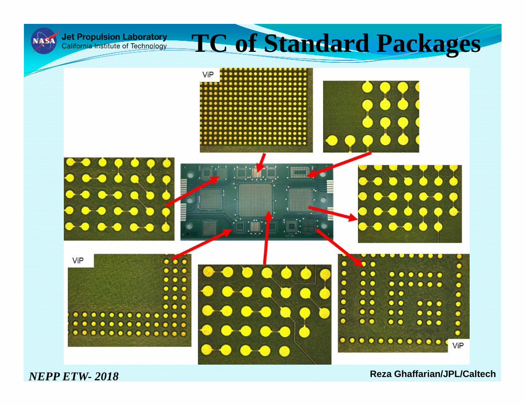
TC of Standard Packages

Reza Ghaffarian/JPL/CaltechNEPP ETW- 2018
� Test matrix covered numerous standard packaging technologies
� FCBGA, FPBGAs, PBGAs daisy-chain package for TC reliability
� Two PCB finish (HASL/ENEPIG) W/WO Microvia
� Most single-side, one double-side mirror image
� TC= (-55°C/100°C), TC = (-55°C/125°C)
� TSC (-65°C/150°C)
FCBGA/PBGA & more

Reza Ghaffarian/JPL/CaltechNEPP ETW- 2018
SN11ENEPIG
SN12HASL
X-rayFCBGA
1924

Reza Ghaffarian/JPL/CaltechNEPP ETW- 2018
FCBGA 1924 on ENEPIG200 TSC (-65°C/150°C)

Reza Ghaffarian/JPL/CaltechNEPP ETW- 2018
200X 200X 200x
200X 200X
FCBGA 1924 on HASL

Reza Ghaffarian/JPL/CaltechNEPP ETW- 2018
PCB Pads
PCB Pads
BGA Pads
BGA Pads
FCBGA 1924 on HASL200 TSC (-65°C/150°C)

Reza Ghaffarian/JPL/CaltechNEPP ETW- 2018
X-ray FPBGA432/ENEPIG

Reza Ghaffarian/JPL/CaltechNEPP ETW- 2018
FPBGA432 on ENEPIG

Reza Ghaffarian/JPL/CaltechNEPP ETW- 2018
SEM/EDS of FPBGA432 on ENEPIGPbSn Balls

Reza Ghaffarian/JPL/CaltechNEPP ETW- 2018
2.5D/3DPackaging Technologies
2D to 2.5 D*Single Chip to Multi-chip
TSV for Interposer
2.5D to 3DTSV 3D SIP
Stack Die PoP
Package on Package (PoP)
3D Wire Bond
3D
Through-silicon Via
3D Wafer-level Packaging
* 2.5D now 2DS (on silicon substrates) and 2DO (on organic substrates)

Reza Ghaffarian/JPL/CaltechNEPP ETW- 2018
3D StackSingle-sided

Reza Ghaffarian/JPL/CaltechNEPP ETW- 2018
3D StackX-ray after TC

Reza Ghaffarian/JPL/CaltechNEPP ETW- 2018
3D StackX-section after TC
Reza Ghaffarian/JPL/CaltechNEPP ETW- 2018
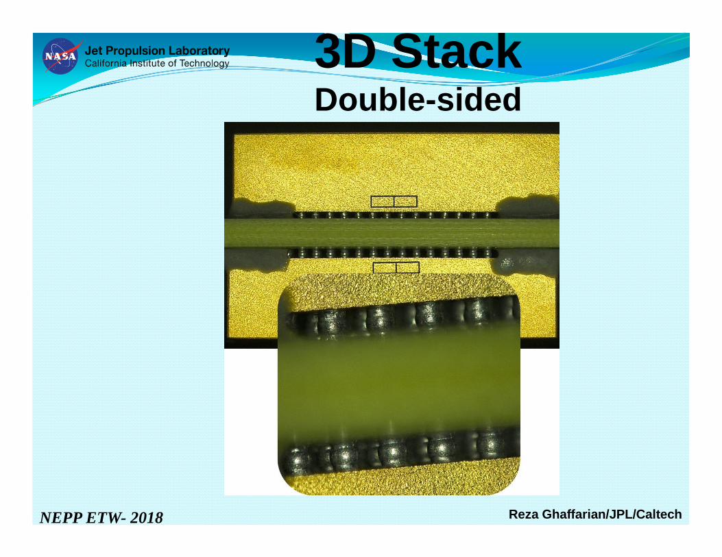
3D StackDouble-sided

Reza Ghaffarian/JPL/CaltechNEPP ETW- 2018
TMV/TSV PackagingStatus
2.5 DSIP
3D TSV TMV
Through Mold Via (TMV)

Reza Ghaffarian/JPL/CaltechNEPP ETW- 2018
� Assembled ten (10) 3DTMV, 9-15 bottom/top parts
� Three assembly styles: Pre-stack, use solder paste for both bottom/top, use solder paste for bottom, flux for top
� No failures to 200 thermal cycles (-55/125C)
� NASA NEPP Report submitted
3D TMV
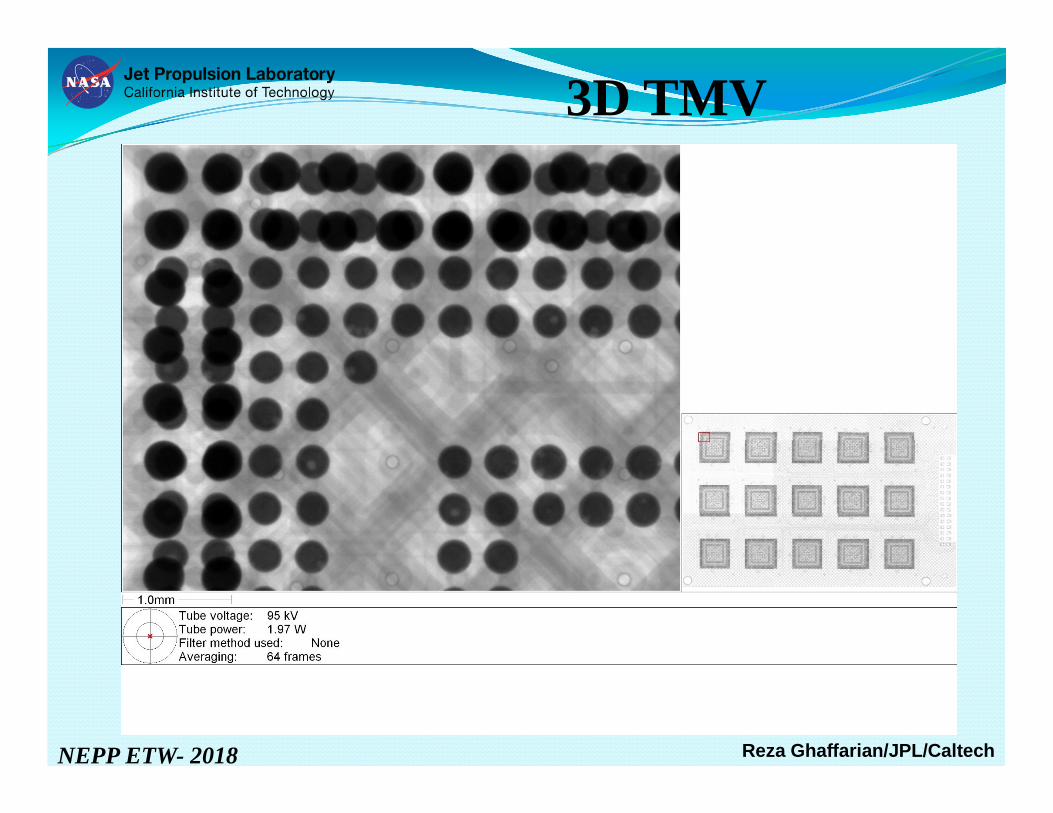
Reza Ghaffarian/JPL/CaltechNEPP ETW- 2018
3D TMV

Reza Ghaffarian/JPL/CaltechNEPP ETW- 2018
3D TMVafter TC
Bottom: Solder PasteTop: Solder Paste
Bottom: Solder PasteTop: Flux Only

Reza Ghaffarian/JPL/CaltechNEPP ETW- 2018
3D TMVSEM after TC/Cut

Reza Ghaffarian/JPL/CaltechNEPP ETW- 2018
3D TMV3D CT Scan after TC/Cut

Reza Ghaffarian/JPL/CaltechNEPP ETW- 2018
3D TMVX-section at 3D Scan
Reza Ghaffarian/JPL/CaltechNEPP ETW- 2018
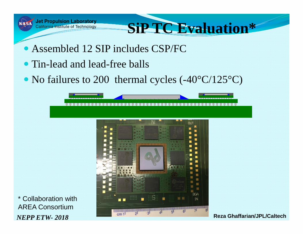
� Assembled 12 SIP includes CSP/FC
� Tin-lead and lead-free balls
� No failures to 200 thermal cycles (-40°C/125°C)
SiP TC Evaluation*
* Collaboration withAREA Consortium

Reza Ghaffarian/JPL/CaltechNEPP ETW- 2018
� Failures at higher cycles
� Early failures and standard failures for CSPs
� Failure due to warpage for FC
SiP TC Evaluation

Reza Ghaffarian/JPL/CaltechNEPP ETW- 2018
Warpage for SiP

Reza Ghaffarian/JPL/CaltechNEPP ETW- 2018
BGA Failure in SiP

Reza Ghaffarian/JPL/CaltechNEPP ETW- 2018
WLP & 3D TSVTC Evaluation
Option 1: Modified WLP TSV to enable PCB manufacturingOption 2: Use interposer for TC

Reza Ghaffarian/JPL/CaltechNEPP ETW- 2018
Summary� Packaging technologies� Standard to WLP and 3DTSV
� NEPP evaluated reliability of numerous packages� FCBGA. FPBGA, 3D stack, WLP, SiP, and 3D TSV� Presented results of numerous TC evaluation
� No failure to 200 TC cycles (–55°/100°C) � FCBGA1924, PBGA896, FPGA, 3D stack� No failure condition verified by daisy-chain or X-section
� Failure to 200 TSC cycles (–65°/150°C) � FPBGA 432 I/O, 0.4 mm pitch failed near 100 cycles
� No failure of TMV assemblies (–55°/125°C)� All paste at board, but solder paste or flux on the top� Pre-stack with paste and then solder onto board
� No failure of SiPs (–40°/125°C)� Effect of top stack on lower failure initiation observed at higher cycle� Various failures including flip-chip at higher cycles
� Design/Assembly of WLP/FOWLP on standard PCB is challenging. Interposer needed� NEPP Test Report on FCBGA/3D stack is on NEPP Website� NEPP Report for TMV/SiP is being released

Reza Ghaffarian/JPL/CaltechNEPP ETW- 2018
The research described in this publication is being conducted at the Jet Propulsion Laboratory, California Institute of Technology, under a contract with the National Aeronautics and Space Administration. Copyright 2018 California Institute of Technology. U.S. Government sponsorship acknowledged.
The author would like to acknowledge the support of the JPL team and industry partners. The author also extends his appreciation to the program managers of the National Aeronautics and Space Administration Electronics Parts and Packaging (NEPP) Program, including M. Sampson, K. LaBel, Dr. D. Sheldon, Dr. J. Evans, and J. Pellish for their support and continuous encouragement.
http://nepp.nasa.gov