rf and if digitization in radio receivers: theory ... · rf and if digitization in radio receivers:...
TRANSCRIPT

NTIA Report 96-328
RF and IF Digitization in Radio Receivers:Theory, Concepts, and Examples
J.A. WepmanJ.R. Hoffman
U.S. DEPARTMENT OF COMMERCERonald H. Brown, Secretary
Larry Irving, Assistant Secretaryfor Communications and Information
March 1996

2
Product Disclaimer
Certain commercial equipment, components, instruments, and materials are identified in this paperto provide some examples of current technology. In no case does such identification implyrecommendation or endorsement by the National Telecommunications and InformationAdministration, nor does it imply that the material or equipment identified is necessarily the bestavailable for the purpose. Furthermore, examples of technology identified in this paper are notintended to be all-inclusive; they represent only a sampling of what is available.

3
CONTENTS
Page
Product Disclaimer . . . . . . . . . . . . . . . . . . . . . . . . . . . . . . . . . . . . . . . . . . . . . . . . 2
1. INTRODUCTION . . . . . . . . . . . . . . . . . . . . . . . . . . . . . . . . . . . . . . . . . . . . . . 5
2. ANALOG-TO-DIGITAL CONVERTERS . . . . . . . . . . . . . . . . . . . . . . . . . . . . . . . 72.1 Sampling Methods and Analog Filtering . . . . . . . . . . . . . . . . . . . . . . . . . . . 7
2.1.1 Sampling at Twice the Maximum Frequency . . . . . . . . . . . . . . . . . . 72.1.2 Out-of-Band Energy . . . . . . . . . . . . . . . . . . . . . . . . . . . . . . . . . . 72.1.3 Realizable Anti-Aliasing Filters . . . . . . . . . . . . . . . . . . . . . . . . . 102.1.4 Oversampling . . . . . . . . . . . . . . . . . . . . . . . . . . . . . . . . . . . . . 102.1.5 Quadrature Sampling . . . . . . . . . . . . . . . . . . . . . . . . . . . . . . . . 112.1.6 Bandpass Sampling for Direct Downconversion . . . . . . . . . . . . . . . 11
2.2 Effects of Quantization Noise, Distortion, and Receiver Noise . . . . . . . . . . . 122.3 Important Specifications . . . . . . . . . . . . . . . . . . . . . . . . . . . . . . . . . . . . 14
2.3.1 Theoretical Signal-to-Noise Ratio Specifications . . . . . . . . . . . . . . 152.3.2 Practical Specifications for Real ADC’s . . . . . . . . . . . . . . . . . . . . 16
2.4 ADC Conversion Methods . . . . . . . . . . . . . . . . . . . . . . . . . . . . . . . . . . . 202.5 ADC Performance vs. Sampling Rate . . . . . . . . . . . . . . . . . . . . . . . . . . . 28
3. DIGITAL SIGNAL-PROCESSING REQUIREMENTS AND LIMITATIONS . . . . . . 303.1 Processors . . . . . . . . . . . . . . . . . . . . . . . . . . . . . . . . . . . . . . . . . . . . . 303.2 Real-Time Operation . . . . . . . . . . . . . . . . . . . . . . . . . . . . . . . . . . . . . . 323.3 Algorithms . . . . . . . . . . . . . . . . . . . . . . . . . . . . . . . . . . . . . . . . . . . . . 33
4. POTENTIAL DEVICES AND METHODS USEFUL IN RADIOS EMPLOYING RF AND IF DIGITIZATION . . . . . . . . . . . . . . . . . . . . . . . . . . . . 36
4.1 Quantization Techniques . . . . . . . . . . . . . . . . . . . . . . . . . . . . . . . . . . . . 364.1.1 Uniform Quantization . . . . . . . . . . . . . . . . . . . . . . . . . . . . . . . . 374.1.2 µ-law Quantization . . . . . . . . . . . . . . . . . . . . . . . . . . . . . . . . . 384.1.3 Adaptive Quantization . . . . . . . . . . . . . . . . . . . . . . . . . . . . . . . 434.1.4 Differential Quantization . . . . . . . . . . . . . . . . . . . . . . . . . . . . . . 44
4.2 Nonlinear Devices for Amplitude Compression . . . . . . . . . . . . . . . . . . . . . 474.2.1 Log Amplifiers . . . . . . . . . . . . . . . . . . . . . . . . . . . . . . . . . . . . 474.2.2 Automatic Gain Control . . . . . . . . . . . . . . . . . . . . . . . . . . . . . . . 49
4.3 Postdigitization Algorithms for Improving Spurious Free Dynamic Range . . . . . . . . . . . . . . . . . . . . . . . . . . . . . . 50
4.4 Sampling Downconverters . . . . . . . . . . . . . . . . . . . . . . . . . . . . . . . . . . . 514.5 Specialized Integrated Circuits . . . . . . . . . . . . . . . . . . . . . . . . . . . . . . . . 52
5. EXAMPLES OF RADIOS USING RF OR IF DIGITIZATION . . . . . . . . . . . . . . . . 53

4
CONTENTS (Cont’d)Page
6. SUMMARY AND RECOMMENDATIONS . . . . . . . . . . . . . . . . . . . . . . . . . . . . 57
7. REFERENCES . . . . . . . . . . . . . . . . . . . . . . . . . . . . . . . . . . . . . . . . . . . . . . . 59
APPENDIX: ACRONYMS AND ABBREVIATIONS . . . . . . . . . . . . . . . . . . . . . . . . 63

The authors are with the Institute for Telecommunication Sciences, National Telecommunications and*
Information Administration, U.S. Department of Commerce, Boulder, CO 80303.
5
RF AND IF DIGITIZATION IN RADIO RECEIVERS: THEORY, CONCEPTS, AND EXAMPLES
Jeffery A. Wepman and J. Randy Hoffman *
Hardware development of analog-to-digital converters (ADC’s) and digital signalprocessors, including specialized integrated circuits, has advanced rapidly withinthe last few years. These advances have paved the way for development of radioreceivers using digitization at the IF and in some cases at the RF. Applications forthese receivers are expected to increase rapidly in areas such as cellular mobile,satellite, and personal communications services (PCS) systems. The constraintsplaced on these receivers due to hardware limitations of these devices areinvestigated in this paper. Some examples of state-of-the-art ADC’s, signalprocessors, and specialized integrated circuits are listed. Various quantizationtechniques, nonlinear compression devices, postdigitization algorithms forimproving dynamic range, sampling downconverters, and specialized integratedcircuits are discussed as they are expected to be useful in the development of thesetypes of receivers. Several examples of radio receivers employing digitization atthe IF and RF are also presented.
Key words: analog-to-digital converters; automatic gain control devices; digital signalprocessors; digitization; logarithmic amplifiers; quantization; radio receivers;sampling downconverters; signal-to-noise ratio; spurious free dynamic range
1. INTRODUCTION
As advances in technology provide increasingly faster and less expensive digital hardware, moreof the traditionally analog functions of a radio receiver will be replaced with software or digitalhardware. The final goal for radio receiver design is to directly digitize the RF signal at theoutput of the receive antenna and therefore implement all receiver functions in either digitalhardware or software. The trend in receiver design is evolving toward this goal by incorporatingdigitization closer and closer to the receive antenna for systems at increasingly higher frequenciesand wider bandwidths. Analog RF front-ends with digitization at either baseband or IF arecurrently being implemented in many arenas.
There is keen interest in replacing analog hardware with digital signal processing in radio receiversfor several reasons. One reason is the potential for the reduction in product development timesince changes can be implemented in software instead of altering the hardware [1]. Digitaltechnology can offer a more ideal performance for implementing signal-processing functions. Therepeatability and temperature stability can be substantially better. Functions that are not

6
implementable in analog hardware can be implemented in software. An example is the design offinite impulse response (FIR) filters that simultaneously can achieve sharp rolloff and linear phase.Another advantage is that digitally implemented signal-processing functions do not require thetuning or “tweaking” typically required in an analog implementation to achieve the desiredperformance [2]. (Proper operation of digital processing circuitry does require some level ofsynchronization, however.) Cost-effective multipurpose radios can be designed to allow receptionof different modulation types and bandwidths simply by changing the software that controls theradio. The final benefit is the cost savings in implementing the receiver.
As radio receiver design evolves so that direct digitization of the RF input signal becomes morecommonplace, these systems will have to go through the process of spectrum certification beforethey can be implemented and used by Government agencies. The process of spectrum certificationincludes an electromagnetic compatibility (EMC) analysis. Development of EMC analysismethodologies and a spectrum certification process for radio receivers using digitization at the RFis required to help the National Telecommunications and Information Administration (NTIA)manage the Federal radio spectrum for Government agencies in the most efficient manner possible.
Methods for analyzing EMC in traditional receivers (such as the superheterodyne) are wellestablished. EMC analysis of these new receivers that utilize digitization of the RF signal at thefront-end may be different. Information currently requested by NTIA for receiver equipmentcharacteristics that is used in the EMC analyses may no longer be relevant for these new types ofreceivers. Detailed knowledge of how these receivers operate is therefore required to help developappropriate methods of EMC analysis. This report provides more information on these types ofradio receivers. In Section 2, we discuss analog-to-digital converters (ADC’s), one of theimportant components needed in radio receivers using digitization at the RF or IF. Therequirements, practical limitations, and potential problems for ADC’s are presented. Section 3includes the signal-processing requirements and limitations for radio receivers that digitize at theRF or IF. Some devices and techniques that may be useful for receivers employing directdigitization of the RF are described in Section 4. These include 1) methods of nonuniformquantization, 2) nonlinear amplitude compression devices, 3) algorithms for improving dynamicrange, 4) sampling downconverters, and 5) specialized integrated circuits. Chapter 5 presentssome examples of radios that digitize at the RF or IF. Chapter 6 provides a brief summary of thisinvestigation and some recommendations for further work in this area.

7
2. ANALOG-TO-DIGITAL CONVERTERS
The ADC is a key component in any radio that uses direct digitization of the RF input signal orthat uses digitization after an initial downconversion to an IF. The other key component is thedigital signal processor (discussed in Section 3).
2.1 Sampling Methods and Analog Filtering
The sampling process is critical for radio receivers using digitization at the RF or IF. The contentof the resulting sampled signal waveform is highly dependent on the relationship between thesampling rate employed and the minimum and maximum frequency components of the analoginput signal. Some common sampling techniques that utilize a uniform spacing between thesamples include sampling at twice the maximum frequency, oversampling, quadrature sampling,and bandpass sampling (also called downsampling or direct downconversion). Samplingtechniques with nonuniform spacing between the samples do exist but they are not widely used andtherefore are not considered in this report.
When a continuous-time analog signal is sampled uniformly, the spectrum of the original signalF(f) is repeated at integer multiples of the sampling frequency (i.e., F(f) becomes periodic). Thisis an inherent effect of sampling and cannot be avoided. This phenomenon is shown graphicallyin Figure 1. Figure 1a shows the spectrum of the original analog signal F(f). Figure 1b showsthe spectrum of the sampled signal F (f) using a sampling rate of f =2f .s s max
2.1.1 Sampling at Twice the Maximum Frequency
The general theorem for sampling a bandlimited analog signal (a signal having no frequencycomponents above a certain frequency f ) requires that the sampling rate be at least two timesmax
the highest frequency component of the analog signal 2f . This ensures that the original signalmax
can be reconstructed exactly from the samples. Figure 1b shows an example of sampling abandlimited signal with a maximum frequency of f at f =2f . Note that the copies of F(f) thatmax s max
are present in F (f) do not overlap. As the sampling rate is increased beyond 2f , the copies ofs max
F(f) that are present in F (f) are spread even farther apart. This is shown in Figure 1c. Samplings
a bandlimited signal at rates equal to or greater than 2f guarantees that spectrum overlap (oftenmax
called aliasing) does not occur and that the original analog signal can be reconstructed exactly[3,4]. Figure 1d shows the spectrum overlap that occurs when sampling at rates less than 2f .max
2.1.2 Out-of-Band Energy
Two practical problems arise when sampling at the 2f rate: defining what a bandlimited signalmax
is for real systems and analog filtering before the ADC stage. A theoretically defined bandlimited

8
Figure 1. Spectrum of: (a) a bandlimited continuous-time analog signal; (b) the signal sampledat f =2f ; (c) the signal sampled at f >2f ; and (d) the signal sampled at f <2f .s max s max s max
signal is a signal with no frequency components above a certain frequency. When considering realsignals such as an RF signal at the input of a radio receiver, however, signals of all frequenciesare always present. While all frequencies are always present, it is the amplitude of thesefrequencies that is the important factor. In particular, the relative amplitude of the undesiredsignals to the desired signal is important. When digitizing an RF or IF signal at the 2f rate inmax
a radio receiver, undesired signals (above one-half the sampling rate) of a sufficient amplitude cancreate spectrum overlap and distort the desired signal. This phenomenon is illustrated in Figure 2.Figure 2a shows the spectrum of the analog input signal with its desired and undesiredcomponents. If this signal is sampled at two times the highest frequency in the desired signal f ,d
the resulting spectrum of the sampled signal F (f) is shown in Figure 2b. Note that spectrums
overlap has occurred here (i.e., the spectrum of the undesired signal occurs within the spectrum

9
Figure 2. Spectrum of: (a) a continuous-time analog signal with a desired and undesiredcomponent and (b) the signal sampled at f =2f .s d
of the desired signal). This causes distortion in the reconstructed desired signal. This effect raisesan important question: “How large do signals occurring above f /2 need to be for the distortions
of the desired signal to be caused predominantly by spectrum overlap and not ADCnonlinearities?” Nonlinearities in the ADC cause spurious responses in the ADC output spectrum.Distortion due to spectrum overlap can be said to predominate distortion due to ADCnonlinearities when the undesired signals appearing in the frequency band from 0 to f /2 due tos
spectrum overlap exceed the largest spurious response of the ADC due to nonlinearities.Therefore, undesired signals appearing in the frequency band from 0 to f /2 due to spectrums
overlap must be lower in power than the largest spurious response of the ADC. In other words,distortion of the desired signal is predominated by ADC nonlinearities (and not spectrum overlap)if signals higher in frequency than f /2 are lower in power than the largest spurious response ofs
the ADC. This can be quite a stringent requirement. Depending upon the details of the radiosystem, this requirement may be eased.
To determine ways to “ease” this requirement, the following questions should be asked: “Howmuch distortion of the desired signal is tolerable?,” “Do the bandwidth and frequency content ofboth the desired signal in the frequency band from 0 to f /2 and the undesired signals above thes
frequency band from 0 to f /2 effect the distortion of the desired signal?” These questions are bests
answered by considering the details of the specific radio system such as the type of sourceinformation (voice, data, video, etc.); the desired signal bandwidth; the modulation and codingtechniques; the undesired signal characteristics (bandwidth, power, and type of signal); and theperformance criterion used to evaluate the reception quality of the desired signal. System

10
simulation is a valuable tool for providing answers to these questions for specific radio systemsand operating environments.
2.1.3 Realizable Anti-Aliasing Filters
Analog filtering before the ADC stage is intimately related to the definition of bandlimiting.Where the definition of bandlimiting involves the content of the signals that may be present,analog filtering before the ADC represents a signal-processing stage where certain frequencies canbe attenuated. It is important to know both the signals that can be present before filtering and theamount of attenuation that the filter offers for different frequencies. With knowledge of both ofthese, the true spectrum of the signal to be digitized can be determined. Sampling at two timesthe maximum desired frequency presents a large and often impractical demand on the filter usedbefore digitization (the anti-aliasing filter). Ideally, an anti-aliasing filter placed before an ADCwould pass all of the desired frequencies up to some cutoff frequency and provide infiniteattenuation for frequencies above the cutoff frequency. Then sampling at f =2f would be twos max
times the cutoff frequency and no spectrum overlap would occur. Unfortunately, practical,realizable filters cannot provide this type of “brickwall” response. The attenuation of real filtersincreases more gradually from the cutoff frequency to the stopband. Therefore, for a given cutofffrequency on a real filter, sampling at two times this cutoff frequency will produce some spectrumoverlap. The steeper the transition from the passband to the stopband and the more attenuationin the stopband, the less the sampled signal will be distorted by spectrum overlap. In general,more complicated filters are required to achieve steeper transitions and higher attenuation in thestopband. Therefore, more complicated filters are required to reduce the distortion in the sampledsignal due to spectrum overlap for a given sampling rate. Limitations on the practicalimplementation of analog filters make high-order, steep rolloff filters difficult to realize. Also,as the steepness of the rolloff is increased, the phase response tends to become more nonlinear.This can create distortion of the desired receive signal since different frequencies within a signalcan be delayed in time by different amounts.
2.1.4 Oversampling
Sampling at rates greater than 2f is called oversampling. One of the benefits of oversamplingmax
is that the copies of F(f) that are present in F (f) become increasingly separated as the sampling rates
is increased beyond 2f . For an analog signal with a given frequency content and a given anti-max
aliasing filter with a cutoff frequency of f , sampling at two times the cutoff frequency producesc
a certain amount of distortion due to spectrum overlap. When sampling at a higher rate, a simpleranti-aliasing filter with a more gradual transition from passband to stopband and less stopbandattenuation can be used without any increase in the distortion due to spectrum overlap. Therefore,oversampling can minimize the requirements of the anti-aliasing filter. The tradeoff, of course,is that faster ADC’s are required to digitize relatively low frequency signals.

11
2.1.5 Quadrature Sampling
In quadrature sampling the signal to be digitized is split into two signals. One of these signals ismultiplied by a sinusoid to downconvert it to a zero center frequency and form the in-phasecomponent of the original signal. The other signal is multiplied by a 90 phase-shifted sinusoidto downconvert it to a zero center frequency and form the quadrature-phase component of theoriginal signal. Each of these components occupies only one-half of the bandwidth of the originalsignal and can be sampled at one-half the sampling rate required for the original signal.Therefore, quadrature sampling reduces the required sampling rate by a factor of two at theexpense of using two ADC’s instead of one.
2.1.6 Bandpass Sampling for Direct Downconversion
Sampling at rates lower than 2f still can allow for an exact reconstruction of the informationmax
content of the analog signal if the signal is a bandpass signal. An ideal bandpass signal hasno frequency components below a certain frequency f and above a certain frequency f .l h
Typically, bandpass signals have f » f - f . For a bandpass signal, the minimum requirementl h l
on the sampling rate to allow for exact reconstruction is that the sampling rate be at least twotimes the bandwidth f - f of the signal.h l
Sampling at a rate two times the bandwidth of a signal is called the Nyquist sampling rate.When the signal is a baseband signal (a signal with frequency content from DC to f ) themax
Nyquist sampling rate is 2f . For bandpass signals, however, the Nyquist sampling rate ismax
2(f - f ). To ensure that spectrum overlap does not occur when sampling rates are betweenh l
two times the bandwidth of the bandpass signal and two times the highest frequency in thebandpass signal, the sampling frequency f must satisfy [4] s
These equations show that only certain ranges of sampling rates can be used if spectrum overlapis to be prevented.
Bandpass sampling can be used to downconvert a signal from a bandpass signal at an RF or IF toa bandpass signal at a lower IF. Since the bandpass signal is repeated at integer multiples of thesampling frequency, selecting the appropriate spectral replica of the original bandpass signalprovides the downconversion function.
Bandpass sampling holds promise for radio receivers that digitize directly at the RF or IF sincethe desired input signals to radio receivers are normally bandpass signals. Theoretically, bandpasssampling allows sampling rates to be much lower than those required by sampling at two or moretimes the highest frequency content of the bandpass signal. This implies that ADC’s with slowersampling rates (and therefore potentially higher performance, lower power consumption, or lowercost) may be used. An important practical limitation, when using bandpass sampling, is that the

12
ADC must still be able to effectively operate on the highest frequency component in the signal.This specification is usually given as the analog input bandwidth for the ADC.
Conventional ADC’s are designed to operate on signals with maximum frequencies up to one-halfthe sampling rate. In other words, conventional ADC’s typically are not suitable for bandpasssampling applications where the maximum input frequencies are greater than the sampling rate.Furthermore, for conventional ADC’s, many manufacturers provide specifications only atfrequencies well below one-half the maximum sampling rate. In general, performance of ADC’stypically degrades with increased input frequency. Therefore, in using ADC’s for frequenciesnear one-half the maximum sampling rate or for bandpass sampling applications, the specificationsof the converter must be determined and carefully examined at the desired input frequencies. Inaddition, when bandpass sampling, stringent requirements on analog bandpass filters (steeprolloffs) are needed to prevent distortion of the desired signal from strong adjacent channelsignals.
2.2 Effects of Quantization Noise, Distortion, and Receiver Noise
This section addresses the relationships between quantization noise, harmonic distortion, andreceiver noise. The ADC’s best suited to RF and IF processing that have widespread availabilityuse uniform quantization. In uniform quantization, the voltage difference between eachquantization level is the same. Other methods of quantization include logarithmic (A-law andµ-law), adaptive, and differential quantization. These methods currently are used in sourcecoding. A discussion of these quantization techniques is given in Section 4.
In uniform quantization, the analog signal cannot be represented exactly with only a finite numberof discrete amplitude levels. Therefore, some error is introduced into the quantized signal. Theerror signal is the difference between the analog signal and the quantized signal. Statistically, theerror signal is assumed to be uniformly distributed within a quantization level. Using thisassumption, the mean squared quantization noise power P isqn
where q is the quantization step size and R is the input resistance of the ADC [5]. In an idealADC, this representation of the quantization noise power is accurate to within a dB for inputsignals that are not correlated with the sampling clock.
If the analog input into an ADC is periodic, the error signal is also periodic. This periodic errorsignal includes harmonics of the analog input signal and results in harmonic distortion.Furthermore, harmonics that fall above f /2 appear in the frequency band from 0 to f /2 due tos s
aliasing.
This harmonic distortion that occurs through the quantization process is quite undesirable in radioreceiver applications; it becomes difficult if not impossible to distinguish the harmonics caused

13
by quantization and the spurious and harmonic components of the actual input signal. Ditheringis a technique that is commonly used to reduce this harmonic distortion.
Dithering is a method of randomizing the quantization noise by adding an additional noise signalto the input of the ADC [6]. Several types of techniques are used for dithering. Perhaps the mostbasic technique adds wideband thermal noise to the input of the ADC. This can be accomplishedby summing the output of a noise diode with the input signal before digitization by the ADC. Thisalso can be achieved by simply placing an amplifier before the ADC and providing enough gainto boost the receiver noise to a level that minimizes the spurious responses of the ADC. Thesetechniques reduce the levels of the spurious responses by randomizing the quantization noise. Inother words, for periodic input signals that would normally produce harmonics in the ADC output,the addition of a dithering signal spreads the energy in these harmonic components into randomnoise, thus reducing the amplitude of the spurious components.
A disadvantage of adding wideband noise to the input of the ADC is that the SNR is degraded.The amount of degradation depends upon the amount of noise power added to the input of theADC. Adding a noise power equal to the quantization noise power degrades the SNR by 3 dB [5].
Two techniques commonly are used to prevent degradation in the SNR while dithering. The firsttechnique filters noise from a wideband noise source before the noise is added to the ADC input.Filtering limits the noise power to a frequency range that is outside of the receiver’s bandwidth.Hence, over the receiver’s bandwidth, the SNR is not degraded.
The other technique used to prevent degradation of the SNR is called subtractive dithering(Figure 3). A pseudorandom noise (PN) code generator is used to generate the dithering signal.The digital output of the PN code generator is converted into an analog noise signal using a digital-to-analog converter. This noise signal is added to the input signal of the ADC. The digital outputof the PN code generator is then subtracted from the output of the ADC, again preserving the SNRof the ADC [7]. An example of dithering, achieved by boosting the receiver system noise withan amplifier, is given in the following paragraphs.
Commercially available ADC’s typically have a full scale range (FSR) of 1-20 V. The FSR of theADC is the difference between the maximum and the minimum analog input voltages to the ADC.Dividing the FSR by the number of quantization levels 2 , where B is the number of bits of theB
ADC, provides the quantization step size q. For an 8-bit ADC with an FSR of 2.5 V, thequantization step size is 9.77 mV. To compute the quantization noise power, the effective inputresistance of the ADC must be known.
Components in radio receivers typically have a 50-ohm input and output impedance. The inputimpedance of ADC’s is usually higher than this and is not well specified. Therefore, wheninterfacing an RF component with an ADC, as is necessary for digitization at the RF or IF, this

14
Figure 3. Block diagram of subtractive dithering.
impedance mismatch must be considered. A simple method of impedance matching is to place a50-ohm resistive load at the input of the ADC. This forces the effective input resistance of theADC to be close to 50 ohms. The quantization noise power then can be computed. Assuming a50-ohm effective input resistance R to the ADC in this example, the quantization noise powerequals -38 dBm. For a noise-limited receiver, the receiver noise power P can be computed asrn
the thermal noise power in the given receiver bandwidth (BW) plus the receiver noise figure (NF).This is given as
For a receiver with a 10-MHz BW and a 6-dB NF, the receiver noise power is -98 dBm.Therefore, a gain of 60 dB is required to boost the receiver noise to the quantization noise powerlevel. For an ADC of higher resolution, less gain would be needed since the quantization noisepower would be smaller. Also, wider receiver bandwidths and higher receiver noise figures wouldrequire less gain since the receiver noise power would be larger. Nevertheless, for most practicalreceiver and ADC combinations, an amplifier with automatic gain control is necessary before theADC. The automatic gain control is designed so that the receiver noise roughly equals thequantization noise power level for low-level signals and the input signal power does not exceedthe ADC’s FSR for high-level signals.
The 2- to 30-MHz single-sideband (SSB) receiver presented in [8] shows an example of a receiverusing this dithering technique. Digitization occurs at the 456-kHz IF after dual downconversion.The Collins Radio Division of Rockwell International uses this type of scheme in many of theirreceivers.
2.3 Important Specifications
In this section, theoretical signal-to-noise ratio (SNR) due to quantization noise and aperture jitteris discussed. Practical specifications for real ADC’s are then presented.
15
(1)
Figure 4. Frequency-spreading of quantization noise power due to oversampling.
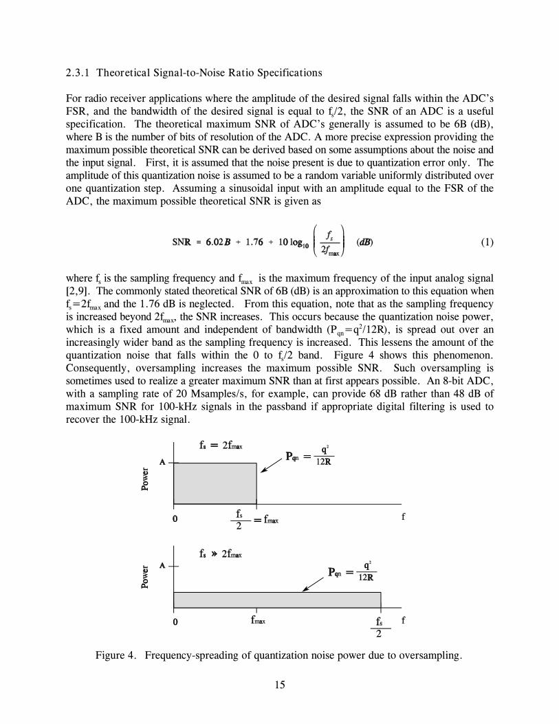
2.3.1 Theoretical Signal-to-Noise Ratio Specifications
For radio receiver applications where the amplitude of the desired signal falls within the ADC’sFSR, and the bandwidth of the desired signal is equal to f /2, the SNR of an ADC is a usefuls
specification. The theoretical maximum SNR of ADC’s generally is assumed to be 6B (dB),where B is the number of bits of resolution of the ADC. A more precise expression providing themaximum possible theoretical SNR can be derived based on some assumptions about the noise andthe input signal. First, it is assumed that the noise present is due to quantization error only. Theamplitude of this quantization noise is assumed to be a random variable uniformly distributed overone quantization step. Assuming a sinusoidal input with an amplitude equal to the FSR of theADC, the maximum possible theoretical SNR is given as
where f is the sampling frequency and f is the maximum frequency of the input analog signals max
[2,9]. The commonly stated theoretical SNR of 6B (dB) is an approximation to this equation whenf =2f and the 1.76 dB is neglected. From this equation, note that as the sampling frequencys max
is increased beyond 2f , the SNR increases. This occurs because the quantization noise power,max
which is a fixed amount and independent of bandwidth (P =q /12R), is spread out over anqn2
increasingly wider band as the sampling frequency is increased. This lessens the amount of thequantization noise that falls within the 0 to f /2 band. Figure 4 shows this phenomenon.s
Consequently, oversampling increases the maximum possible SNR. Such oversampling issometimes used to realize a greater maximum SNR than at first appears possible. An 8-bit ADC,with a sampling rate of 20 Msamples/s, for example, can provide 68 dB rather than 48 dB ofmaximum SNR for 100-kHz signals in the passband if appropriate digital filtering is used torecover the 100-kHz signal.

The SNR is often (and more accurately) called the signal-to-noise plus distortion ratio (SINAD) when1
distortion is included with the noise (as in this case).
16
Besides being limited by the quantization step size (resolution), the SNR of the ADC also islimited by aperture jitter. Aperture jitter is the variation in time of the exact sampling instant.Aperture jitter can be caused externally by jitter in the sampling clock, or internally since thesampling switch does not open at precise times. Aperture jitter causes a phase modulation of thesampled signal and thus results in an additional noise component in the sampled signal [10]. Themaximum analog input frequency of the ADC is limited by this aperture jitter since the SNR dueto aperture jitter (SNR ) degrades as the input frequency increases. The SNR is given asaj aj
where t is the aperture jitter of the ADC [2]. For sampling at f =2f , both the SNR due toa s max
quantization noise and the SNR due to aperture jitter can be combined to give the overallSNR [11].
2.3.2 Practical Specifications for Real ADC’s
The SNR in a real ADC can be determined by measuring the residual error. Residual error is thecombination of quantization noise, random noise, and nonlinear distortion (i.e., all of theundesired components of the output signal from the ADC). The residual error for an ADC isfound by using a sinusoidal input into the ADC. An estimate of the input signal is subtracted fromthe output of the ADC; the remaining signal is the residual error. The mean squared (MS) powerof the residual error then is computed. The SNR then is found by dividing the mean squaredpower of the input signal by the mean squared power of the residual error.1
A specification sometimes used for real ADC’s instead of the SNR is the effective number of bits(ENOB). This specification is defined as the number of bits required in an ideal ADC so that themean squared noise power in the ideal ADC equals the mean squared power of the residual errorin the real ADC.
The spurious free dynamic range (SFDR) is another useful specification for ADC’s. Onedefinition of the SFDR assumes a single tone sinusoidal input into the ADC. Measurement of thisSFDR is made by taking the Fast Fourier Transform (FFT) of the output of the ADC. Thisprovides the frequency spectrum of the output of the ADC and is plotted as the ADC output powerin dB vs. frequency. The SFDR is then the difference between the power in the sinusoidal inputsignal and the peak power of the largest spurious signal in the ADC output spectrum. An exampleof determining the SFDR from the ADC output spectrum is shown in Figure 5. In this idealizedADC output spectrum, the input signal is a 10-MHz sinusoid. Various spurious responses areshown. The SFDR is 50 dB.

17
Figure 5. Example ADC output spectrum showing the spurious free dynamic range.
SFDR allows one to assess how well an ADC can detect simultaneously a very small signal in thepresence of a very large signal. Hence, it is an important specification for ADC’s used in radioreceiver applications. A common misconception is that the SFDR of the ADC is equivalent to theSNR of the ADC. In fact, there is typically a large difference between the SFDR and the SNRof an ADC. The SNR is the ratio between the signal power and the power of the residual error.The SFDR, however, is the ratio between the signal power and the peak power of only the largestspurious product that falls within the band of interest. Therefore, the SFDR is not a directfunction of bandwidth; it does not necessarily change with a change in bandwidth, but it may.Since the power of the residual error includes quantization noise, random noise, and nonlineardistortion within the entire 0 to f /2 band, the power of the residual error can be much higher thans
the peak power of the largest spurious product. Hence, the SFDR can be much larger than theSNR [5]. A practical example of this can be seen from the specifications for the Analog DevicesAD9042 monolithic ADC. With a 19.5-MHz analog input signal, 1 dB below full scale (the full-scale input is 1 V ), the typical SFDR specification is 81 dB while the SNR specification isp-p
66.5 dB (from -40 - +85 °C) [12].
The SFDR specification is useful for applications when the desired signal bandwidth is smallerthan f /2. In this case, a wide band of frequencies is digitized and results in a given SNR. Thes
desired signal then is obtained by using a narrowband digital bandpass filter on this entire band

18
of frequencies. The SNR is improved by this digital-filtering process since the power of theresidual error is decreased by filtering. The SFDR specification for the ADC is important becausea spurious component still may fall within the bandwidth of the digital filter; hence, the SFDR,unlike the SNR, does not necessarily improve by the digital-filtering process. However, severaltechniques are available to improve the SFDR. Dithering (discussed in Section 2.2) improves theSFDR of ADC’s. Additionally, postdigitization-processing techniques such as state variablecompensation [13], phase-plane compensation [14], and projection filtering [15] have been usedto improve SFDR.
For an ideal ADC, and in practical sigma-delta ( ) converters, the maximum SFDR occurs ata full-scale input level. In other types of practical ADC’s, however, the maximum SFDR occursat input levels at least several dB below the full-scale input level. This occurs because as the inputlevels approach full-scale (within several dB), the response of the ADC becomes more nonlinearand more distortion is exhibited. Additionally, due to random fluctuations in the amplitude of realinput signals, as the input signal level approaches the FSR of the ADC, the probability of thesignal amplitude exceeding the FSR increases. This causes additional distortion from clipping.Therefore, it is extremely important to avoid input signal levels that closely approach the full-scalelevel in ADC’s. Prediction of the SFDR for practical ADC’s is difficult, therefore measurementsare usually required to characterize the SFDR.
In the preceding discussion on SFDR, a sinusoidal ADC input signal was assumed. However,intermodulation distortion (IMD) due to multitone inputs is important in ADC’s used for widebandradio receiver applications. To characterize this IMD due to multitone inputs, another definitionof the SFDR could be used. In this case, the SFDR is the ratio of the combined signal power ofall of the multitone inputs to the peak power of the largest spurious signal in the ADC outputspectrum. A current example of test equipment to generate multitone inputs produces up to 48tones.
The noise power ratio (NPR) specification is useful in applications such as mobile cellular radio,where the spectrum of a signal to be digitized consists of many narrowband channels and whereadjacent channel interference can degrade system performance. Particularly, the NPR providesinformation on the effectiveness of an ADC in limiting crosstalk between channels [13].
The NPR is measured by using a noise input signal into the ADC. This noise signal has a flatspectrum that is bandlimited to a frequency that is less than one-half the sampling frequency.Additionally, a narrow band of frequencies is removed from the noise signal using a notch filter.This noise spectrum is used as the input signal to the ADC. The frequency spectrum of the outputof the ADC then is determined. The NPR then is computed by dividing the power spectral densityof the noise outside the frequency band of the notch filter by the power spectral density of thenoise inside the frequency band of the notch filter [5].
When using an ADC in a bandpass-sampling application where the maximum input frequency intothe ADC is actually higher than one-half the sampling frequency, the full-power analog inputbandwidth is an important specification. A common definition (although not universal) of full-power analog input bandwidth is the range from DC to the frequency where the amplitude of theoutput of the ADC falls to 3 dB below the maximum output level. This assumes a full-scale input

19
signal to the ADC. Typically, the ADC is operated at input frequencies below this bandwidth.Aside from full-power analog input bandwidth, it is important to examine the behavior of the otherspecifications such as SNR, SFDR, and NPR at the desired operating frequencies since thesespecifications typically vary with frequency. In addition to the SNR, SFDR, and NPR of realADC’s being a function of frequency, they are also a function of input signal amplitude. Table 1provides a summary of the important ADC specifications for radio receiver applications.
Table 1. Summary of ADC Specifications for Radio Receiver Applications
Specification Application Definition
Signal-to-NoiseRatio (SNR)
Desired Signal BWEqual to f /2s
Spurious FreeDynamic Range
(SFDR)
Desired Signal BWLess Than f /2s
Noise Power Ratio(NPR)
Desired SignalSpectrum ContainsMany Narrowband
Channels
Full-Power AnalogInput BW Bandpass Sampling
Range from DC to Frequency Where OutputAmplitude Falls to 3 dB Less Than Maximum **
With an input signal having a bandlimited, flat noise spectrum and a narrow band of frequencies removed by a*
notch filter.For a full-scale input signal.**
When testing an ADC, it is important to ensure that all quantization levels are tested. For singletone inputs, the relationship between the input signal frequency and the sampling rate must bechosen so that the same small set of quantization levels is not tested repeatedly. In other words,the samples should not always occur at the same amplitude levels of the input signal. Forexample, using an input frequency of f /8 is a poor choice since the same eight amplitude levelss
are sampled every period of the input signal (assuming that the input signal and the sampling clockare phase coherent) [16]. The histogram test can be used to ensure that all quantization levels aretested. In the histogram test, an input signal is applied to the ADC and the number of samples thatare taken at each of the 2 quantization levels are recorded. In an ideal ADC this histogram isB
identical to the probability density function of the amplitude values of the input signal. Comparingthe histogram to the probability density function of the input signal gives an indication of thenonlinearity of the ADC. An examination of the histogram reveals whether all of the differentquantization levels are being tested. When no samples are recorded for a given quantization level,

20
this level is either not being tested by the testing procedure (input signal and sampling rate) or theADC is exhibiting a missing code. A missing code is a quantization level that is not present inthe output of a real ADC that is present in the output of an ideal ADC. Missing codes are fairlyrare in currently available ADC’s in general and do not occur in converters.
2.4 ADC Conversion Methods
Many methods for implementing ADC’s currently exist. Several of the most common techniquesare presented below. The counter ADC uses a digital-to-analog converter (DAC) and increasesthe output of this DAC one quantization level at a time using a counter circuit until the output ofthe DAC equals the amplitude of the analog signal at a given time. The output of the counter thenprovides the digital representation of the analog input voltage. A major drawback to this type ofconverter is that it is fairly slow. An improvement to the counter type ADC is the tracking ADC.This type of converter is similar to the counter ADC except that an up-down counter is used inplace of the ordinary counter. In this ADC, the output of the internal DAC is compared to theanalog input signal. If the amplitude of the analog input signal is greater than the output of theDAC, the counter counts up; if it is less than the output of the DAC, the counter counts down.The tracking ADC is much faster than the counter ADC when there are only small changes in theamplitude of the input signal. For large changes in the input signal amplitude this type of ADCis still fairly slow.
The counter and tracking ADC’s belong to the feedback class of ADC’s. The successive-approximation ADC also belongs to this class. This type of ADC again uses a DAC in a feedbackloop. For a conversion with this ADC, a register is used to set the most significant bit (MSB) inthe DAC to 1. The output of the DAC is compared to the amplitude of the analog input. If theDAC output is greater than the analog input, the MSB of the DAC is cleared, otherwise it is keptset to 1. The next significant bit of the DAC is then set to 1 and the output of the DAC again iscompared to the amplitude of the analog input. If the DAC output is greater than the analog input,this bit is cleared. This process continues for all B bits of the DAC. The input of the DACprovides the output of the ADC. The conversion is made in B steps making this technique quiteefficient and hence reasonably fast. Successive-approximation is one of the most popular ADCtechniques.
The parallel or flash ADC is used for applications that require the fastest possible digitization.In the current state-of-the-art technology, sampling rates on the order of 500-1000 Msamples/s foran 8-bit ADC most likely imply that a flash ADC is being used. This type of converter uses abank of 2 - 1 voltage comparators in parallel where B is the number of bits of the ADC. TheB
analog input signal is applied to one input on all of the voltage comparators while the other inputto each comparator is a reference voltage corresponding to each of the 2 - 1 quantization levels.B
The reference voltages typically are generated by a voltage divider network. All comparators withreference voltages below the analog input signal produce a logical 1 output. The remainingcomparators, with reference voltages equal to or above the input signal, produce a logical 0output. The outputs of the comparators are then combined in a fast decoder circuit to generatethe output digital word of the ADC. Therefore, conversion takes place in only two steps (voltagecomparison and decoding), making this technique the fastest of the commonly available

21
techniques. A major limitation of this type of ADC is the large number of comparators requiredin the implementation. For a B-bit flash ADC, 2 - 1 comparators are needed. Since an 8-bitB
ADC requires 255 comparators and a 9-bit ADC requires 511 comparators, flash ADC’s of morethan 8 bits typically are not available commercially. Linearity is a problem in flash ADC’s asobserved in degraded SFDR performance.
One technique used to implement high-speed ADC’s combines two separate B-bit ADC’s (usuallyflash ADC’s) to produce a single ADC with a resolution of 2B bits. For example, two 4-bitconverters can be combined to provide an 8-bit converter. In this technique, the first 4-bit ADCdigitizes the analog input. The output of the ADC is then converted back into an analog signalusing a DAC. This signal then is subtracted from the original input analog signal producing adifference signal. This difference signal is then amplified and digitized using the second 4-bitADC. The amplifier gain is set to provide a full-scale input signal into the second ADC. Theoutputs of both 4-bit ADC’s then are combined using digital error correction logic to produce an8-bit output representing the analog input signal [17]. This type of ADC is called a two-stagesubranging ADC. Subranging ADC’s with up to five stages are available. Signal delays(sometimes called pipeline delays) increase with each additional stage and must be considered inthe design of subranging ADC’s. Subranging ADC’s exhibit a repetitive nonlinearity due to thenature of digitizing difference signals. This is visualized best by considering a ramp input into anideal ADC representing the first stage of a subranging ADC. The transfer function of the idealADC is shown in Figure 6a while the ramp input is shown in Figure 6b. The output of the firstADC is a quantized version of the ramp as shown in Figure 6c. Subtracting a reconstructedversion of the input ramp from the quantized version, produces a repetitive ramp differencewaveform that repeats 2 times where B is the number of bits in the first ADC. This differenceB
signal (shown in Figure 6d) is amplified to produce a full-scale input to the second ADC.Therefore, the differential nonlinearity in the second ADC is exercised 2 times. (DifferentialB
nonlinearity is defined as the deviation of any quantization step in the ADC from q, the theoreticalquantization step size of the ADC.)
Subranging ADC’s are becoming very popular since they can achieve high-speed operation withhigh resolution. They require far fewer comparators for a given resolution than flash ADC’s.While the internal ADC’s within a subranging ADC have traditionally been flash ADC’s, othertypes of ADC’s may be used. For example, a new architecture, the cascaded magnitude amplifier,has been used in the Analog Devices AD9042 (a 12-bit, 41-Msamples/s subranging ADC). Thisarchitecture provides a very high-speed conversion and greatly reduces the number of comparatorsrequired in the internal ADC’s.
The cascaded magnitude amplifier (MA) ADC consists of B-1 MA’s in series and a singlecomparator placed in series after the last MA. A diagram showing the operation of the cascadedMA ADC is given in Figure 7. Referring to this figure, the first MA compares the input signalto a voltage level V /2 where V is the full-scale input voltage of the ADC. If the input signal isfs fs

22
Figure 6. (a) Ideal ADC transfer function; (b) input ramp signal; (c) output (quantized) rampsignal; and (d) repetitive ramp difference signal.
greater than V /2, the bit representing this MA is set to 1. If the input signal is less than V /2, thefs fs
bit representing this MA is set to 0. Therefore, this first MA divides the full-scale voltage intotwo regions and the bit representing this MA is set according to the region in which the inputvoltage falls. The next (second) MA uses the output of the first MA as its input. As shown in Figure 7, thesecond MA divides each of the two regions defined by the first MA into two additional regions.If the input voltage to the first MA is between V and V /2, the second MA determines if the inputfs fs
signal is between V and 3V /4 or between 3V /4 and V /2. The bit representing this MAfs fs fs fs

23
Figure 7. Operation of the cascaded magnitude amplifier ADC.

24
Figure 8. First-order ADC.
then is set to 1 or 0, respectively. Conversely, if the input voltage to the first MA is between 0and V /2, the second MA determines if the input signal is between V /2 and V /4 or between V /4fs fs fs fs
and 0. The bit representing this MA then is set to 0 or 1, respectively.
Each subsequent MA (and the final comparator) further subdivides the regions in a similarmanner, providing all of the necessary quantization levels (Figure 7 shows operation up to thethird MA). Because of the way that the bit representing an MA is set (as seen in Figure 7), theoutput bits from each MA form a Gray code that represents the input signal voltage. In the Graycode, only one bit changes in the code word from one quantization level to another.Determination of the output bits is dependent upon the input signal propagating through thecascaded MA’s only. Very high-speed operation is achieved because the response time of theamplifiers is very fast.
Integrating ADC’s are another category of converters. They convert the analog input signalamplitude into a time interval that is measured subsequently. The most popular methods withinthis category of ADC’s are the dual slope and charge balancing methods. While these types ofADC’s are highly linear and are good at rejecting input noise, they are quite slow.
A relatively new type of ADC is the converter. The first-order converter is the mostbasic converter (Figure 8). It consists of a modulator, a digital filter, and a decimator.To understand how this converter works, an understanding of oversampling, noise shaping, digitalfiltering, and decimation is required.
The operation of the converter relies upon the effects of oversampling. converters usea very low-resolution quantizer (typically a 1-bit quantizer) and sample at a rate much greater than2f . As discussed previously, sampling at rates faster than 2f provides an improvement in themax max
SNR of the ADC. This occurs because the quantization noise, which is a fixed amount, is spread

25
(2)
out over a greater bandwidth as f increases beyond 2f . This improvement in SNR due tos max
oversampling causes the low-resolution quantizer to appear to have a much higher resolution.This apparent higher resolution can be quantified by the ENOB and is found from
This equation shows that the SNR must increase by approximately 6 dB in order for the ENOBto increase by 1 bit. As shown in (1), the sample rate f must be increased to four times greaters
than 2f in order for the SNR to increase by approximately 6 dB. Each subsequent increase ofmax
6 dB in the SNR requires a further increase in sampling rate of four times.
As seen from (1) and (2), to achieve an ENOB of 12 bits using a 1-bit quantizer, a sampling rateover 4 million times faster than 2f is required. This obviously is not practical and shows thatmax
converters must use other techniques in addition to oversampling.
The other key component in converters is the integrator that is placed before the 1-bitquantizer. This integrator functions as a low-pass filter for the desired signals occurring at orbelow f and as a high-pass filter for the quantization noise in the ADC. This shapes themax
quantization noise (which is normally flat across the band from 0 to f /2) so that very little of thiss
noise occurs in the desired signal’s band (0 to f ). Most of the quantization noise is shifted tomax
frequencies above f . This process is called noise shaping and is shown in Figure 9. The resultsmax
of this noise shaping are that the desired apparent resolution (ENOB) can be achieved with muchless oversampling than is predicted by (1) and (2).
The effects of the integrator on the quantization noise of the converter can be seenmathematically by considering a linearized model of the modulator portion of the converter.The block diagram of this model is shown in Figure 10. The quantizer is modeled as a unity gainamplifier with quantization noise added. Looking at this model in the frequency domain, theoutput of the modulator Y(s) is given as
where X(s) is the input signal, H(s)=1/s is the transfer function of the integrator, and Q is the quantization noise. This expression can be rewritten as

26
Figure 9. Noise shaping in ADC’s.
Figure 10. Linearized model of the modulator.
This shows that at low frequencies (s<<1) the output is primarily a function of the input signalX(s) and not the quantization noise. For high frequencies (s>>1), Y(s) is primarily a functionof the quantization noise [18].
More than one integration and summing stage can be used in the modulator to provide even morenoise shaping. Third and even higher-order converters have been designed. (The numberof integrators determines the order of the modulator.) Higher-order modulators further decreasethe amount of quantization noise in the desired signal’s band by placing more of the quantizationnoise above f . Therefore, higher-order converters can provide the same apparent resolutionmax

27
with less oversampling than lower-order converters [19]. modulators higher than second-order provide some difficult design challenges. Instability becomes possible and must beconsidered carefully in the design.
After the modulator, a digital filter is used. This digital filter is used to 1) filter thequantization noise above f and 2) prevent aliasing when the signal is decimated. Decimationmax
is a process of reducing the data rate by resampling a discrete-time signal at a lower rate.Decimation is useful in converters because the oversampling creates a data rate that is muchhigher than 2f . After filtering the quantization noise, the highest frequency component of themax
desired signal is only f . Therefore, the required sampling rate only needs to be 2f to fullymax max
reconstruct the desired input signal. Decimation is performed by saving only one out of every Msamples to reduce the data rate to (or a little higher than) 2f .max
Decimation may be combined with digital filtering for more efficient processing. FIR filters canbe used to provide both filtering and decimation at the same time. This is true because the FIRfilter output needs to be computed for only one out of every M input samples. Conversely, infiniteimpulse response (IIR) filters cannot be used for decimation because they rely on all of the inputsamples to produce the proper output. IIR filtering, if desired, can be performed after decimation.
The converters described are designed to operate on baseband signals. A new type ofconverter, the bandpass converter, shows great potential for radio receiver applications fordigitization at the RF or IF. This converter architecture is identical to the traditional converter except that the integrators are replaced by bandpass filters and a bandpass digital filterafter the modulator is used. Use of bandpass filters instead of integrators shapes thequantization noise such that it is moved both below and above the desired band of frequencies.This provides a bandpass region of low quantization noise. Bandpass converters are currentlya very promising research and development topic.
The converter has a couple of advantages over the more traditional types of ADC’s. Becauseof the high sampling rate, the attenuation requirements on the anti-aliasing filter can be lessened.Additionally, an improvement in the linearity of the ADC results in an improved SFDR. Thisadvantage results from using a 1-bit or other low-resolution quantizer. One disadvantage of converters that are currently available is that they typically are limited to signal bandwidths below150 kHz (for a 12-bit ENOB).
The design of high-speed ADC’s usually incorporates both a sample-and-hold amplifier (SHA) anda quantizer. Many ADC’s provide a SHA as an integral part of the ADC. External SHA’s alsocan be used with ADC’s but this requires careful design considerations of the SHA and ADCspecifications, in addition to timing and interface issues between the external SHA and the ADC.
The purpose of the SHA in ADC applications is to keep the input signal constant during the ADCconversion. While there are many different SHA implementations, all SHA’s consist of four basiccomponents: an input amplifier, capacitor, output buffer, and switching circuit. An example SHAshowing the basic components is given in Figure 11. The input amplifier provides a high inputimpedance to the input signal and supplies the necessary current to charge the hold capacitor.When the switch closes, the SHA operates in the track mode and the voltage on the hold capacitor

28
Figure 11. Example showing the basic components of a sample-and-hold circuit.
follows the input signal. When the switch opens, the SHA operates in the hold mode. Ideally,the voltage on the hold capacitor remains at its value before the switch opened. Since it has a highinput impedance, the output buffer prevents the hold capacitor from discharging significantly. Thehold command controls the operation of the switch and determines when the SHA is in the trackor hold mode [20].
Sometimes SHA’s are called track-and-hold amplifiers (THA’s). The name used depends on howthe device is used. When the device spends most of its time in the hold mode and just a short timein track mode (enough time to take a sample of the input), the device is called a SHA. When thedevice spends only a short time in the hold mode and most of its time in the track mode, it iscalled a THA [21].
For radio receiver applications, typically high-speed ADC’s are required, especially for directdigitization of the RF or digitization of wideband IF. Because of this, successive-approximation,subranging, flash, and bandpass ADC’s are the most likely types of ADC’s to be used forthese applications.
2.5 ADC Performance vs. Sampling Rate
The performance of ADC’s continues to improve at a rapid rate. For radio receiver applicationsusing digitization at the RF or IF, ADC’s with both high sampling rates and high performance aredesired. Unfortunately, there is a tradeoff between these two requirements. As a general trend,although not always true, the higher the performance of the ADC, the lower its maximumsampling rate will be. The goal of direct digitization at the RF in radio receivers at increasinglyhigher frequencies and wider bandwidths is one of the forces driving the development of higher-performance, faster ADC’s. Digital sampling oscilloscopes are another example of applicationsthat encourage the development of higher-performance, faster ADC’s.
Interleaving is a common technique used to increase the sampling rate beyond the capability of asingle ADC. In this technique, multiple ADC’s of the same type are staggered in time to achievehigher sampling rates. Each ADC is offset in time from the preceding ADC. For uniform sample

29
spacing, this offset is determined by dividing the time interval between samples of a single ADCby the total number of ADC’s to be used. The interleaving technique is used extensively in digitalsampling oscilloscopes. Examples of current high-speed ADC technology showing maximum sampling rates for variousADC resolutions are given in Table 2. The low-resolution (6- or 8-bit), high sampling rate ADC’sare typically implemented as flash ADC’s and therefore are limited in SFDR.
When selecting an ADC for a specific radio receiver application, in addition to the sampling rate,one must consider critical specifications that characterize the ADC performance such as the SNR,SFDR, NPR, and full-power analog input bandwidth. In certain applications such as channelizedPCS and mobile cellular systems, instead of digitizing the entire band with a single high-speedADC, parallel ADC’s used to digitize narrower bandwidths are often practical ADC architectures.In this case, ADC’s with better performance can be used since the demands of a high samplingrate are relieved.
Table 2. Examples of Current High-Speed ADC Technology
Resolution (Number of Bits) Sampling Rate(Msamples/s) Manufacturer
6 4000 Rockwell International
8 1000 Signal Processing Technology
8 2000* Hewlett-Packard
8 3000**
10 70 Pentek
12 50 Hughes Aircraft
12 100**
14 24 Hughes Aircraft
18 10 Hewlett-Packard
8000 Msamples/s with interleaving.*
Device in development; work is being sponsored b y the Advanced Research Projects Agency (ARPA) of the U.S.**
Department of Defense.

30
3. DIGITAL SIGNAL-PROCESSING REQUIREMENTS AND LIMITATIONS
Besides ADC’s, digital signal processing is another key element in radios using digitization of theRF or IF. The amount of time required for signal processing is of critical importance in radioreceiver applications. The required processing time is a function of the received signal bandwidth,the speed of the processor, and the number and complexity of the algorithms required to performthe needed radio receiver operations. These operations are application-specific and may includesome or all of the following: downconversion, filtering, multiple access processing,demultiplexing, frequency despreading, demodulation, synchronization, channel decoding,decryption, and source decoding [22,23]. Because of the wide variety of algorithms possible inradio receiver applications, digital signal-processing limitations are more difficult to discuss thanADC’s.
The intent of this section is to discuss the requirements and limitations of digital signal processing.It is not intended to provide a detailed presentation of the wide variety of digital signal-processingtechniques and algorithms that are available. Many books and papers are available to providedetailed information on digital signal-processing techniques and algorithms. One fundamentalbook on digital signal processing is [24].
3.1 Processors
Many different processors are available to provide digital signal processing. These processorsvary substantially in speed of operation, physical size, and cost. Speed is usually a criticalrequirement in selecting a processor. Other factors including dynamic range, arithmetic precision,cost, and size are also important considerations when choosing a processor.
A common method used to increase total processing speed beyond that of a single processor is toemploy multiple processors operating in parallel. Assuming a given processor, by putting moreand more of these processors together and operating them in parallel, higher and higher processingspeeds can be achieved. This, of course, also increases power consumption, size, and cost. Many radio receiver applications require processors with small physical size and relatively lowcost. For these cases, single chip processors are the preferred choice. Single chip processors canbe general purpose microprocessors (such as the Intel 80486), digital signal processors (such asthe Texas Instruments TMS320C40), or specialized integrated circuits for dedicated processingtasks (such as the Harris HSP50016 Digital Downconverter). Some specialized radio receiverapplications may not be bound by stringent physical size and cost limitations. Therefore,processors of all types are considered in this report, ranging from single chip general purposemicroprocessors to supercomputers.
Computations in digital signal processing can be performed using fixed-point arithmetic orfloating-point arithmetic, although many of the computations require floating-point arithmetic.The advantage of floating-point arithmetic over fixed-point arithmetic is that it permits the use ofnumbers with a much greater dynamic range. This is important in many digital signal-processingoperations.

31
In fixed-point arithmetic, the position of the decimal point in the register where each operand isstored always is assumed to be the same. In floating-point arithmetic, each operand is representedby a number stored in a register representing a fraction or integer. A number stored in a secondregister specifies the position of the decimal point of the number stored in the first register. Someprocessors do not have floating-point hardware and require floating-point operation to beimplemented in software. Software implementation of floating-point arithmetic is typically muchslower than hardware implementation.
Because floating-point operations are so important in digital signal processing, the speed ofprocessors is often specified in terms of millions of floating-point operations per second(MFLOPS). This parameter allows comparison of the processing speed of different processorsand also allows determination of the time required to execute certain algorithms.
Many different benchmarks (such as the SPEC benchmarks, Whetstone, Dhrystone, and Linpack)are used to compare speeds between processors. Each benchmark provides a number indicatingthe relative speed of processing based on testing varying tasks. Results from the application ofa benchmark to different processors can be compared. However, results between differentbenchmarks, in general, should not be compared. While these benchmarks are useful forcomparing processor performance, the parameter chosen to compare processing speeds betweenprocessors in this report is the theoretical peak MFLOPS. This parameter was chosen due to itsease of availability for virtually all floating-point processors, its lack of dependence on specificbenchmarking algorithms, and its relevancy to dedicated applications used in implementation ofa radio receiver. The theoretical peak MFLOPS parameter gives the maximum possible speed ofperformance for the processor. It is found by computing the number of floating-point additionsand multiplications (using the processor’s full precision) that can be performed during a given timeinterval [25].
Some examples of the processing speed of various types of processors ranging from single chipprocessors to supercomputers are presented in Table 3. This table only gives a sampling of therange of capabilities that exist in digital signal processing. Many other processors, with varyingcapabilities, either exist or have been proposed. In addition, new developments with increasingcapabilities are announced all the time. An extensive listing of processing speeds for manydifferent computers is found in [25].
In certain situations, especially in the high-throughput case, overall processing performance is notlimited by the processor speed but by the maximum data transfer rates of the peripheralcomponents such as memory or I/O (input/output) ports. The inclusion of these factors inplatform evaluation should not be ignored when choosing a processor.

32
Figure 12. Real-time processing for block data using a single processor.
Table 3. Examples of Processing Technology
ProcessingSpeed *
Numberof
ProcessorsPlatform Manufacturer and Model
50 MFLOPS 1 DSP Chip Texas Instruments TMS320C40
120 MFLOPS 1 DSP Chip Analog Devices ADSP-21060/62
400 MFLOPS 8 VME Board Pentek 4285
800 MFLOPS 16 Computer Workstation SUN Sparc 2000
6.48 GFLOPS 4 Supercomputer Convex C4/XA-4
32 GFLOPS 4 Supercomputer Hitachi S-3800/480
184 GFLOPS 3680 Massively ParallelComputer
Intel Paragon XPS140
236 GFLOPS 140 Massively ParallelComputer
National Aerospace Laboratory Numerical Wind Tunnel (Japan)
Theoretical peak processing speed.*
3.2 Real-Time Operation
For most radio receiver applications, real-time operation is important. In many types ofprocessing, such as computing Fast Fourier Transforms (FFT’s), the data is partitioned into blocksof a finite length. Processing is performed on the entire block of data. In this block typeprocessing, assuming a single processor, real-time operation essentially means that all processingon a given block of data (including any required data transfers) is completed before all of the nextblock of data to be processed is captured. This concept is illustrated in Figure 12 [26].

33
Figure 13. Real-time processing for block data using two processors.
If the processing time (including any required data transfers) is longer than the time required tocapture all of the next block of data (again assuming a single processor), data collection must bestopped until the processing is completed. At that time data collection may resume. Under theseconditions some of the input data is missed and is not processed. This is an example of processingthat does not take place in real time. Depending upon the application and the amount of data lost,this may not be acceptable.
This problem can be alleviated by using two or more processors operating cooperatively. Thisgeneral technique is called multiprocessing and is used frequently. To illustrate howmultiprocessing can be used to speed up overall data throughput, consider the previous exampleof data partitioned into data blocks but with two processors available instead of one. As shownin Figure 13, processor 1 operates on one block of data and processor 2 operates on the next blockof data. The processors continue to operate on alternating data blocks. The processed data outputis obtained by switching back and forth between the outputs of the two processors. This issometimes called a “ping-pong” technique. Using this technique, the processing time of eachprocessor can take longer than the time to capture the next block of data and still provide real-timeoutput. The processing time cannot exceed the time to capture the next two blocks of data,however. This technique can be extended to more than two processors to achieve even fasteroverall data throughput.
3.3 Algorithms
Providing a general discussion on algorithms used for implementing radio receiver functions isdifficult. This is due to the wide variety of types of receivers as well as the various ways ofimplementing the required receiver operations for each type of receiver. In short, algorithms arehighly application-specific. The details of the many potential algorithms used in radio receiversare beyond the scope of this report. It is beneficial, however, to look at an example algorithm toobserve the methodology in determining algorithm complexity vs. the potential for real-timeoperation. This type of assessment is crucial for radio receivers that use digitization at the RF orIF.
The FFT is an example of an algorithm frequently used in digital signal-processing and radioreceiver applications. The FFT transforms time-domain samples of received signals into a set of

There are many different FFT algorithms available requiring different numbers of floating-point operations.2
N log N commonly is used as an approximation for the number of floating-point operations required in computing2
an FFT.
34
frequency-domain samples, allowing operations on the received signals to be performed directlyin the frequency domain. These received signals are typically bandpass signals when digitizationoccurs at the RF or IF. These bandpass signals may be digitized using either sampling at twicethe maximum frequency, bandpass sampling, or oversampling. The FFT also can be applied tosignals that have been downconverted to baseband but the signal must be split into co-phase andquadrature-phase components before digitization unless coherent downconversion has been used.
Regardless of the sampling method employed, the resolution of the transformed signal in thefrequency domain is a function of both the time spacing between the samples of the signal t inthe time domain and the number of samples N used in the computation of the FFT. The frequencyspacing between samples in the frequency domain is then given as
The maximum frequency of the spectrum is then
since there are N/2 samples in the FFT computed from N real-valued time-domain samples.
(Actually, there are (N/2)+1 samples in the FFT ranging from DC to f if both DC and f aremax max
included.) For a fixed N-point FFT (i.e., an FFT computed from N real-valued time-domainsamples), the frequency spacing between the frequency domain samples f must be changed inorder to change the maximum frequency of the spectrum. That requires changing the time spacing
t between the time-domain samples. By decreasing t and holding N constant, the time durationof a block of N samples is reduced and the maximum frequency of the spectrum is therebyincreased. Therefore, for fixed values of N, the higher the maximum frequency desired, theshorter the duration of the block of N samples must be. With a fixed number of samples N, agiven processor, and a given FFT algorithm , the processing time to compute an N-point FFT is2
fixed. For real-time operation, this computation of the FFT (including any other requiredprocessing such as windowing and any required data transfers) must be performed within the timetaken to capture all N samples of the current data block assuming that a single processor is used.A parameter called real-time bandwidth then can be defined as the maximum frequency that canbe processed in real time.
To achieve real-time processing, careful consideration of processor speed, the signal bandwidth(data rate), the number of computations required in implementing the signal-processingalgorithms, and the speed of any necessary data transfers is required. An example showing howto estimate the amount of processing power required for real-time analysis is given below. For

35
this example, the simplified case of looking at the time required to compute an FFT isinvestigated. While this example shows the methodology used to determine a required processingspeed, the processing required for radio receiver applications normally would involve much morethan computing a single FFT. In this simplified example, it is assumed that an input signal issampled at a fixed rate and that the only processing performed on the sampled input signal is theFFT. No other processing (such as windowing or averaging) is performed. Data transfer timeis also neglected.
Assuming a bandlimited input signal with a maximum frequency of 5 MHz, the 2f samplingmax
rate would be 10 Msamples/s. For this sampling rate, the time between samples t is 100 ns.Assume that FFT’s are computed from blocks of N=1024 samples. Therefore, it takesN t = 102.4 µs to capture a block of data. The number of floating-point operations (actuallymultiplications) required to compute an N-point FFT is estimated as N log N. Therefore, roughly2
2
10,240 floating-point operations are required for the 1024-point FFT. In order to achieve real-time processing in the single processor case, the FFT must be computed within the time periodrequired to capture a block of data (102.4 µs). The minimum required processing speed is thenfound by
In this simplified case, the minimum processing speed is 100 MFLOPS. One can then comparethe required processing speed to the processing speeds available for different types of processorssuch as those listed in Table 3.

Section 4.1, Quantization Techniques (from pages 36-47), iscurrently unavailable for distribution over the Internet.Please contact Jeff Wepman via e-mail [email protected] for further information.
36
4. POTENTIAL DEVICES AND METHODS USEFUL IN RADIOSEMPLOYING RF AND IF DIGITIZATION
This section describes some methods and devices that may be useful in implementing radioreceivers where digitization occurs at the RF or IF. These methods and devices probably will beconsidered in the design of future radio receivers as the digitization of received signals progressestoward the receive antenna. Various quantization techniques are discussed in detail since theauthors believe that this area has great potential for use in radio receiver applications. Nonlinearcompression devices are discussed, including log amplifiers and automatic gain control devices.Postdigitization algorithms for improving the SFDR provide extended dynamic range capabilityfor presently available ADC’s. Sampling downconverter technology is introduced. Thistechnology is based on the theory of bandpass sampling and may be coupled with ADC technologyto provide improved ADC performance for bandpass sampling applications. Finally, specializedintegrated circuits for digital signal-processing tasks required in radio receiver applications arementioned. An example of this type of technology, the Harris HSP50016 digital downconverter,is presented.
4.1 Quantization Techniques

Section 4.1, Quantization Techniques (from pages 36-47), iscurrently unavailable for distribution over the Internet.Please contact Jeff Wepman via e-mail [email protected] for further information.
37

Section 4.1, Quantization Techniques (from pages 36-47), iscurrently unavailable for distribution over the Internet.Please contact Jeff Wepman via e-mail [email protected] for further information.
38

Section 4.1, Quantization Techniques (from pages 36-47), iscurrently unavailable for distribution over the Internet.Please contact Jeff Wepman via e-mail [email protected] for further information.
39

Section 4.1, Quantization Techniques (from pages 36-47), iscurrently unavailable for distribution over the Internet.Please contact Jeff Wepman via e-mail [email protected] for further information.
40

Section 4.1, Quantization Techniques (from pages 36-47), iscurrently unavailable for distribution over the Internet.Please contact Jeff Wepman via e-mail [email protected] for further information.
41

Section 4.1, Quantization Techniques (from pages 36-47), iscurrently unavailable for distribution over the Internet.Please contact Jeff Wepman via e-mail [email protected] for further information.
42

Section 4.1, Quantization Techniques (from pages 36-47), iscurrently unavailable for distribution over the Internet.Please contact Jeff Wepman via e-mail [email protected] for further information.
43

Section 4.1, Quantization Techniques (from pages 36-47), iscurrently unavailable for distribution over the Internet.Please contact Jeff Wepman via e-mail [email protected] for further information.
44

Section 4.1, Quantization Techniques (from pages 36-47), iscurrently unavailable for distribution over the Internet.Please contact Jeff Wepman via e-mail [email protected] for further information.
45

Section 4.1, Quantization Techniques (from pages 36-47), iscurrently unavailable for distribution over the Internet.Please contact Jeff Wepman via e-mail [email protected] for further information.
46

47
4.2 Nonlinear Devices for Amplitude Compression
As discussed in Section 4.1.2, logarithmic compression at the input to the quantizer can improvethe SNR by making it independent of the input signal variance. In actual implementation, wheresystem noise defines a minimum signal input amplitude, this form of compression can be achievedthrough the use of log amplifiers. Likewise, by using variable gain, it is possible to adapt thesignal amplitude to the characteristics of the quantizer. This, too, can be implemented by usingautomatic gain control (AGC) amplifiers. Both log amplifiers and AGC amplifiers are discussedin greater detail below [30-33].
4.2.1 Log Amplifiers
There are several different types of log amplifiers, each suited to different applications. Commonto all is some form of logarithmic compression of signal parameters. A simple operationalamplifier circuit that uses the nonlinear (logarithmic) characteristics of a p-n junction can be used[34]; however, these circuits suffer from temperature variations, limited dynamic range, and slowrise times. Depending on the application, these circuits may or may not be adequate. A morepowerful technique is the approximation of the logarithmic function using the summation of linear(or curved) lines. Typically these are implemented with differential amplifiers using integratedcircuit technology and may be purchased as discrete components or built into the front-endreceiver circuitry. There are three basic types of these log amplifiers: detector log videoamplifiers, successive detection log amplifiers, and true log IF amplifiers.
Detector log video amplifiers are suited to applications where phase and frequency informationis not necessary. The envelope of the input signal simply is converted to a log-compressed videosignal at the output. Total input dynamic range of these amplifiers is generally 50 dB. A typicalapplication might be the demodulation and logarithmic compression of an amplitude-modulatedsignal.

48
Figure 23. Limited IF output power as a function of the input signal power.
The successive detection log amplifier provides two outputs. One is the same as the detector logvideo amplifier output, described above. The other is a limited IF signal. The former providesamplitude information expressed in logarithmic form and the latter provides phase and frequencyinformation. The limited IF signal is a copy of the input signal except that its amplitude variationis compressed and limited by a transfer function similar to that in Figure 23. This figure showsthe limited IF output power as a function of the input signal power. Typically these amplifiershave a total input dynamic range of 80 dB. A successive detection log amplifier recently has beenannounced by Microphase, Inc. that provides a 100-dB input dynamic range.
The “true” logarithmic IF amplifier is called so because the IF output is a bipolar logarithmicfunction of the IF input signal (without any limiting). This amplifier may also have an output thatis the same as the detector log video amplifier. Due to the dual-polarity of the output signal, theseamplifiers function well in logarithmic IF applications. As might be expected, there is somedeviation from the true logarithmic curve (toward a more linear function) as signals approach zero,but this is not generally a problem if the system noise power is set to the minimum signal inputamplitude of the log amplifier (typically -80 dBm). These amplifiers also generally have a totalinput dynamic range of 80 dB. In addition, they inherently have low phase shifts over widevariations in input signal power.
Logarithmic amplifiers have wide instantaneous dynamic range. Instantaneous dynamic rangemeans that at any point in time, all signals within the dynamic range of the amplifier appear at the

49
output. Take for an example, an input containing two signals, one at -5 dBm and one at -75 dBm.For a logarithmic amplifier with an 80-dB dynamic range, it is possible to maintain the integrityof both signals at the output, but in a compressed form. Instead of the log amplifier, consider avariable attenuator placed before a fixed-gain amplifier. With the same input consisting of boththe -5-dBm and -75-dBm signals, assume that the fixed-gain amplifier would saturate if noattenuation was used. Therefore, the attenuation of the variable attenuator must be increased toprevent amplifier saturation. In doing so, the noise figure of the combination of the variableattenuator and the fixed-gain amplifier will increase. This may cause the smaller signal (-75 dBm)to be overpowered by the noise and go undetected. Logarithmic amplifiers are, therefore, goodfor processing multiple signals where small signals are present simultaneously with large signals.Logarithmic amplifiers must be used carefully in receiver systems, however. Being nonlineardevices, they may cause distortion of the input signals. A careful analysis of the effects ofdistortion on the desired received signals must be performed.
4.2.2 Automatic Gain Control
AGC is used to normalize the output signal level despite variations in input signal power. Atypical AGC device operates using a feedback loop whereby the power of the output of a variablegain device (amplifier or attenuator) is sampled and used to adjust the gain of the variable gaindevice itself. In this way, the output power is maintained at a relatively constant level. Theresponse time of the AGC loop is perhaps the most critical design parameter and is dependentupon the application. Generally the AGC device is adjusted to react fast enough to normalize theoverall power but slow enough to maintain the desired information content of the signal.Depending upon the application, the control voltage for the variable gain device may be used todecompress the output signal after digitization.
Typically AGC devices can have a total dynamic range of 80 dB. But because they operate byadjusting the gain of the system, the instantaneous dynamic range is much lower than that forlogarithmic amplifiers. Therefore, these systems generally are better suited for narrowerbandwidth systems where individual signals are isolated by appropriate filtering before the AGC.AGC’s, unlike logarithmic amplifiers, are not effective in receivers where weak desired signalsneed to be detected in the presence of strong undesired signals.
AGC devices can be purchased as discrete components or built into the front-end receivercircuitry. As with any feedback system, stability is an important consideration. In radio receiverapplications that use an AGC device before an ADC, there should be enough gain in the systemso that the system noise at the output of the AGC device prior to digitization is slightly greaterthan the quantization noise power of the digitizer. To maximize the SNR, the normalized outputof the AGC device should be set as large as possible without causing the ADC to overload orgenerate excessive spurious responses. A more detailed discussion of AGC devices can be foundin [35].

50
4.3 Postdigitization Algorithms for Improving Spurious Free Dynamic Range
As previously mentioned, there are numerous postdigitization techniques for optimizing thequantization process. Many of these techniques are used to increase the SNR of the quantizer byimproving the predictor characteristics of differential quantization schemes. Another area ofpostdigitization processing provides compensation for the nonlinearities that occur in practicalimplementations of ADC’s. As discussed in Section 2 of this report, these nonlinearities producespurious signals that can reduce significantly the SFDR of the ADC. The purpose of thiscompensation is to suppress the spurious responses below the noise in the frequency band from0 to f /2. Two of these techniques, phase-plane and state variable compensation, are discusseds
below [13,14].
Both techniques are used to identify a set of correction factors that can be used to compensate forany nonlinearity throughout the full amplitude range of the ADC. In phase-plane compensation,the procedure for correcting the digitized signal is as follows: The input signal is split into twoseparate signals. One signal is fed into the ADC and the other is sent through an analogdifferentiator and then digitized by a second ADC. The differentiated signal is used to determinethe instantaneous slope of the signal. The output of both ADC’s then is used to determine thecorrection factor to be applied to the ADC output representing the digitized input signal. A tableconsisting of correction factors for each possible combination of quantization level andinstantaneous slope is developed for an individual ADC based on measurements of that particularADC. This table then is stored in RAM and is used to provide the correct ADC output for anygiven input signal amplitude. Studies using this technique show as much as a 15- to 16-dB (about2.5 bits) improvement in the SFDR over uncompensated ADC’s [14]. This improvement,however, is restricted to a narrow frequency band well below f /2.s
In an effort to improve the SFDR for all frequencies in the 0 to f /2 frequency band, a states
variable compensation technique was also proposed. This type of compensation is implementedby applying the input signal to an ADC and splitting the output of the ADC into two signals. Oneof these signals is used without modification while the other is delayed by a single clock cycle (onesample of the input signal). The two outputs, representing the quantization levels for the presentand previous ADC outputs, then are used to determine the correction factor to be applied to thepresent ADC output. A table of correction factors for each possible combination of present andprevious quantization levels is developed for an individual ADC based on measurements of thatparticular ADC. As in phase-plane compensation, this table is stored in RAM and is used toprovide the correct ADC output for any given input signal amplitude. Tests using this techniquealso show as much as a 16-dB improvement in the SFDR over the entire 0 to f /2 frequency bands
for the particular sampling rate.
While compensation techniques require additional hardware and testing of individual ADC’s, theycan improve the SFDR of the ADC significantly without increasing its resolution (number of bits).In essence, they bring the characteristics of the ADC closer to the theoretical expectation of itsperformance. An underlying assumption in these techniques, however, is that the ADCcharacteristics are static. Testing of ADC’s has shown that for most ADC’s this is a validassumption [14].

51
4.4 Sampling Downconverters
The 6300 series sampling downconverters manufactured by Watkins-Johnson are an example ofa technology potentially useful in the RF front-end of radio receivers. These samplingdownconverters are microwave devices that use bandpass sampling techniques to downconvert anRF signal (typically in the 2- to 18-GHz range) to an IF signal (typically at 70 MHz up to500 MHz). In its current configuration, the sampling downconverter functionally performs in thesame manner as the conventional mixer. However, the device is actually a sample-and-hold circuitthat uses a step recovery diode (SRD) to generate a sampling pulse train from a sinusoidal “clock”frequency. The sample-and-hold circuits in these downconverters are designed to work in the 2-to 18-GHz range, far higher in frequency than the sample-and-hold circuits integral to mostADC’s. In the future, this technology may be coupled with high-resolution quantizers to producebandpass sampling ADC’s with a high analog input frequency capability and the high resolutionof quantizers that would operate at much lower frequencies. Use of these samplingdownconverters for radio receiver applications requires some careful considerations, however.The frequency content of the input must be bandlimited properly to prevent spectrum overlap inthe desired signal output as with any bandpass sampling scheme. These downconverters do suffera higher conversion loss than conventional mixers. The maximum specified conversion loss forthe 6300 series sampling downconverters can be anywhere from 13-25 dB depending on thespecific model. Typical conversion loss for conventional mixers ranges from roughly 5-9 dB.As with any downconverter, spurious suppression must be considered carefully. Thespecifications for the Watkins-Johnson 6300 series sampling downconverters state a minimum 15-dBc spurious suppression at a -10-dBm RF input level [36]. (This spurious suppression does notinclude the local oscillator (LO) signal leakage at the IF port or the 2 harmonic of the IF signal.)nd
More typically, even a bad spur would be 25 dBc with the -10-dBm RF input level. Operation atlower RF input levels will provide even better spurious suppression [37]. These types of devicesmay be very useful for future radio receiver front-ends and ADC’s.
It is tempting to compare the spurious suppression of the sampling downconverter to that ofconventional mixers. While this comparison could be made for a specific mixer, it is not possibleto make any general conclusions. While there are several types of conventional mixers, double-balanced mixers are the industry standard [38]. Even within the double-balanced mixer type, thereare several different classes of mixers. These classes of mixers include class 1, class 2, and class3 mixers. Class 2 mixers require more LO power and have better spurious suppression than class1 mixers. Similarly, class 3 mixers require more LO power and have better spurious suppressionthan class 2 mixers. The higher the mixer class, the more LO power is required but the better thespurious suppression is. In addition to the different classes of mixers, spurious suppression is afunction of LO and RF input power levels and frequencies. While there are specifications onmixers that help predict spurious suppression, spurious suppression for a specific mixer shouldbe determined by measurement over a well-defined set of conditions [38].

52
4.5 Specialized Integrated Circuits
As digitization in radio receivers moves closer to the receive antenna, more of the traditionallyanalog receiver functions will be replaced with digital signal-processing algorithms. In addition,the area of digital communications requires extensive digital signal processing. While the speedof general digital signal processors continues to increase, specialized integrated circuits (IC’s)can, in general, digitally implement radio receiver functions faster. Use of these specialized IC’sshould be quite prevalent in radio receiver applications of the future.
A current example of this type of specialized IC is the single chip digital downconverter. Digitaldownconversion offers a clear advantage over conventional analog downconversion by providingmore precise frequency control of the LO and by providing a more ideal mixing operation.Current digital downconverters can control LO frequencies to within less than .01 Hz out ofseveral MHz and can provide mixing with over 100 dB of SFDR. In addition, on-chip filters canbe programmed to produce almost any desired bandwidth while preserving linear phase. Incontrast to analog equivalents, these chips provide reproducible component accuracies that do notdegrade over time or temperature.
The Harris HSP50016 is a programmable monolithic digital downconverter capable of extractinga narrow baseband signal from a wideband input bandpass signal (RF or IF) [39,40]. The digitaldownconverter multiplies a digitized wideband input signal by samples representing both an in-phase LO and a quadrature-phase LO to produce in-phase and quadrature-phase baseband signals.Next, the digital downconverter filters the in-phase and quadrature-phase signals to extract thechannel of interest. It then decimates the output to a sampling rate of twice the maximumfrequency of the signal of interest. The digital downconverter can also be configured to providea downconverted version of the input bandpass signal at a new IF. The HSP50016 can operateon 16-bit data at a rate of up to 52 Msamples/s [41].
53
5. EXAMPLES OF RADIOS USING RF OR IF DIGITIZATION
This section describes several radio receivers (currently existing or in development) employingdirect digitization at the RF or IF. Digitization at the IF is becoming increasingly popular. Manyradio receivers using this digitization currently are being developed. While direct digitization ofthe RF is a future design goal, few of these systems are in existence today except perhaps forfrequencies below the HF band. In general, since many radio receivers using digitization at theRF or IF are currently in development, information about them is quite difficult to obtain. Thereceivers discussed below are a small sampling of these systems.
The dynamic signal analyzer is an excellent example of technology that uses direct digitization ofthe RF. The dynamic signal analyzer digitizes the input signal and provides various processing,display, and data storage options. A common signal-processing function is performing an FFTon an input signal and thereby providing a frequency domain display of the input signal. The HP3587S is an example of this type of analyzer. This particular signal analyzer is implemented asa VXIbus system; the VXIbus is a standard modular instrument architecture that allows customconfiguration of various measurement devices in a compact frame under computer control. Theconfiguration of the HP 3587S includes a 10-Msample/s, 18-bit digitizer. This high-resolutionADC provides a maximum SFDR of 110 dB. An amplifier is used before the digitizer to set thesystem (random) noise power slightly above the quantization noise power. The system noisefigure is then determined by this amplifier and is specified to be 14 dB. The signal analyzercontains a DSP module that can compute 250 MFLOPS. With this processor, a 1-MHz real-timebandwidth is achieved [42].
The HP1486A is a VXIbus signal-processing module currently in development that can process9 billion math operations per second. It achieves this high processing speed by using application-specific integrated circuits (ASIC’s) along with performing computations as 28-bit fixed-pointarithmetic. This module was designed for communication signal processing and can provide high-speed demodulation of both analog and digital communications signals. Processing speed isclaimed to be fast enough to provide real-time demodulation of signals in the proposed HDTVdigital transmission format. The HP1486A accepts data input up to 30 Msamples/s using a high-speed local bus. The receiver functions it can perform include: fixed and adaptive filtering;downconversion; extraction of signal amplitude, phase, and frequency information; resampling;adaptive clock and carrier synchronization; and symbol decoding. A general purpose DSP blockis also available for more customized processing. These functions are individually programmableand can be used in a wide variety of combinations to implement various types of radioreceivers [43].
A few years ago, the Novotel Communications Corporation (Calgary, Canada) was working ona global positioning system (GPS) receiver at 1.575 GHz using direct digitization of the RF. Inaddition to the challenges presented by direct digitization at this input frequency, the receiverdesign needed to be small, lightweight, inexpensive, and consume little power. A receiver usingbandpass sampling techniques was considered; however, Novotel found that the receiver designwas not feasible from a cost standpoint. Additionally, a sample-and-hold amplifier that wouldperform well at 1.575 GHz was not available commercially at that time so the technical feasibilitywas also in question.

54
The Honeywell Technology Center is developing an integrated avionics radio that digitizes andprocesses wideband IF signals between 100 and 1300 MHz [44]. The frequency bands that thesystem operates over include:
108-118 MHz VHF Omni Range and Instrument Landing System (ILS) Locator 118-137 MHz VHF Voice (Including Air Traffic Control Operations)329-335 MHz Instrument Landing System Glide Path960-1215 MHz Electronic Aids to Air Navigation (DME/Mode S)
Postdigitization filtering is used to isolate individual signals along with proprietary hardware toextend receiver dynamic range. Due to the developmental nature of this system, any furtherdetails (such as the IF bandwidth, dynamic range, sampling rate, ADC, processor hardware, andtypes of processing) are considered proprietary.
The SEA Corporation currently is producing a portable handheld transceiver operating in the 220-to 222-MHz band that uses digitization at the IF. SEA also is developing receivers for variousapplications in the 3- to 30-MHz band [45]. The 220- to 222-MHz band has 5-kHz channelbandwidths and therefore, requires sophisticated modulation techniques that generally depend ondigital signal processing. Amplitude-companded single-sideband modulation (ACSSB) is beingutilized with transmit tone in band (TTIB). However, discussions are underway to migrate todigital modulation. These receivers digitize IF signals at bandwidths slightly greater than thechannel, and use bandpass sampling techniques for further downconversion. The system uses a12-bit digitizer with a predigitization, 20-dB step AGC device.
Due to the very high dynamic range of input signal amplitudes present in the HF band, andlimitations in the SFDR of high-speed ADC’s currently available commercially, direct digitizationat the RF in HF receivers is currently unrealistic [2]. There has been some recent activity,however, in digitization of the IF in HF radio receivers. An example design for an HF SSB radioreceiver employing digitization at the IF is described in [10]. This SSB receiver uses a traditionalsuperheterodyne front-end with two conversion stages to generate a 16-kHz wide IF signalcentered at 456 kHz. An ADC, operating in a bandpass-sampling mode, samples the IF signal at96 kHz thereby translating the desired replica of the spectrum to an IF centered at 24 kHz. Digitalsignal processing is then used to convert the IF signal to a baseband signal with an in-phase andquadrature-phase component. Decimation is then used to reduce the sample rate and allow thesignal processing to take place in real time. The SSB signal is then digitally demodulated andconverted to an analog signal for output.
Digitization at the wideband IF is being used in some receivers for cellular and PCS base stations.A potentially large market exists for these types of receivers. One example base station, theWatkins-Johnson Base , uses a receiver that digitizes at the wideband IF. The Base base stations2 2
can be used for cellular or PCS applications by simply interchanging the RF front-end. Thereceiver in the Base base station performs an initial downconversion and then digitizes up to a 15-2
MHz bandwidth at the IF. Digital signal processing is then used for channelization, filtering,tuning, and demodulation. The capability of digitizing up to a 15-MHz bandwidth permitsdigitization of either the entire mobile-to-base station cellular frequency block A or block B witha single receiver. Digitization of an entire, licensed, mobile-to-base station PCS frequency block

55
also can be achieved. The Steinbrecher and Airnet Corporations also produce cellular and PCSbase stations that use wideband IF digitization.
There are several advantages of receivers in cellular or PCS base stations that digitize thewideband IF over traditional receivers used in analog cellular base stations. First, analog cellularbase stations require one receiver per cellular channel. Only one wideband receiver is requiredfor all of the cellular channels in a cell using a nonsectorized cell. Sectorized cells require onewideband receiver for all of the cellular channels used in a sector. Because of this, receivers thatdigitize at the wideband IF are cheaper, smaller, and consume less power than analog receiversin cellular base stations. Since filtering, demodulation, and signal processing are all performeddigitally, the audio quality is claimed to be better than in analog receivers [46]. Perhaps one ofthe greatest advantages is that the receivers can receive multiple telephone calls with differing air-interface standards simultaneously. The receiver can be reconfigured with software and canoperate with any air-interface standard. These standards include the advanced mobile phoneservice (AMPS), narrowband AMPS (N-AMPS), time-division multiple access (TDMA), cellulardigital packet data (CDPD), and code-division multiple access (CDMA) [47].
Speakeasy is a new, joint-service military radio transceiver currently in development whosereceiver uses digitization at the IF. The project is being managed by the Air Force RomeLaboratory. In Phase I of this project, the Speakeasy concept was demonstrated by implementinga VME-based radio operating over 2- 2000 MHz using digitization of the IF at bandwidths up toapproximately 10 MHz. General purpose, programmable DSP’s were used for radio receiveroperations whenever possible. When general-purpose DSP’s were not fast enough to performcertain operations, application specific processors and dedicated digital hardware were used.
Two general modes of operation are available for the VME-based Speakeasy radio: a narrowbandmode where an approximately 200-kHz IF bandwidth is digitized, and a wideband mode wherean approximately 10-MHz bandwidth is digitized. Currently, two separate ADC’s are used forthese two modes. The narrowband mode uses a high-resolution ADC while the wideband modeuses a lower-resolution, faster ADC. The eventual goal is to use only one ADC for both modeswhen ADC’s of sufficient resolution and sampling rate become available.
The VME-based Speakeasy radio allows selection (from a menu) of the types of signals that a userwants to transmit and receive. Currently, up to two types of signals can be processed (receivedor transmitted) simultaneously. The ultimate goal is to provide a capability to process four typesof signals simultaneously. Speakeasy can process various types of amplitude, frequency, andphase-modulated signals as well as spread spectrum signals for analog and digital voice and datacommunication.
The goal of Phase II of the Speakeasy project is to provide a more compact and enhanced versionof the VME-based radio developed in Phase I that will emulate more than 15 existing militaryradios [48].
Both direct broadcast satellite (DBS) and digital audio broadcast (DAB) systems transmit variousforms of digitally modulated signals. Receivers for these systems can use either traditionaldemodulators (employing analog circuitry) after downconversion to IF, or digitization at the RF

56
or IF before demodulation. Traditional demodulators require no analog-to-digital conversionbefore demodulation. When using digitization at the RF or IF, demodulation is performed usinga digital signal processor or dedicated digital-processing hardware.
The Advanced Wireless Technologies AWT2002 is a variable data rate BPSK/QPSK demodulatoron a single IC. It is designed to operate on IF signals that have been digitized with a 6-bit ADC.Demodulation is accomplished digitally in this IC as opposed to demodulation requiring analogcircuitry. The currently available version of this IC operates at a 2-Msymbol/s rate; however, afuture version targeted for DBS systems will support symbol rates up to 31.5 Msymbols/s.Digitization at the RF or IF and then digital demodulation, like that provided by the AWT2002,may prove to be very useful in applications such as DBS and DAB.
Digitization at the RF or IF can be employed by receivers in radio propagation measurementsystems. One example of a receiver that uses digitization at the wideband IF is in the recentlypatented digital sampling channel probe (DSCP). The DSCP was developed in a joint effortbetween the Institute for Telecommunication Sciences and Telesis Technologies Laboratory, Inc.The probe is ideal for making outdoor impulse response measurements to characterize widebandpropagation in the radio channel [49].
The DSCP operates by transmitting an RF carrier modulated by a PN code over a radiopropagation channel. The transmitted signal, modified by the propagation channel, then isreceived, downconverted to an IF, and digitized. After digitization at the IF, the complex impulseresponse of the radio propagation channel is generated via digital signal processing. Digitizationat the IF enables the DSCP to measure an impulse response much faster than the traditional analogsliding correlator probe. This allows better characterization of rapidly changing propagationchannels.
Many different system configurations are available with the DSCP. Current configurations usecommercially available equipment such as RF signal generators, spectrum analyzers, digitaloscilloscopes, and personal computers to achieve a high degree of flexibility and to minimizesystem setup time for specific field studies. Both the transmitter and receiver have a dual-channelcapability allowing for transmission and reception with various combinations of two different PNcodes, carrier frequencies, antenna polarizations, and antenna spacings. While the DSCP typicallyhas been used to make impulse response measurements around 900 and 1850 MHz, it can beconfigured to accommodate measurements over an even broader range of frequencies.
In the typical configuration, the null-to-null bandwidth of the probe is 20 MHz, providing a delayresolution of 100 ns and a maximum measurable delay of 51 µs. The probe can be configuredeasily for wider bandwidths (finer time resolution) and different maximum delays. Recentimprovements to the probe include the ability to measure absolute time and Doppler spread.Future plans include expanding the probe to multiple channels to help analyze the potential benefitsof advanced antenna systems and antenna signal processing [49,50].

57
6. SUMMARY AND RECOMMENDATIONS
The key factors in radio receivers where digitization occurs at the IF or RF are analog-to-digitalconversion and digital signal processing. Although not discussed in this paper, digital-to-analogconversion is also a factor for applications requiring analog output (such as voice). Because of therapid advances in hardware development of ADC’s, DAC’s, digital signal processors, andspecialized IC’s, development of radio receivers using digitization at the IF (and in some cases atthe RF) is becoming increasingly popular.
Hardware limitations of ADC’s, digital signal processors, and DAC’s place constraints ondigitization at the IF and RF in radio receivers. It was shown that digitization at the RF, ingeneral, requires some type of bandlimiting (filtering) and amplification before the actualdigitization takes place. The required amount of filtering and amplification is application-specific.ADC performance is improving rapidly. However, there is a tradeoff; one can get either highsampling rates or high resolution, but not both simultaneously. Therefore, the high sampling rateADC’s required for wide bandwidth applications may not have sufficient SFDR. Digitization atthe RF is now being considered for satellite receivers since a large SFDR is not a necessity, veryhigh sampling rate ADC’s already exist, and even faster ADC’s are being developed. For receiverapplications requiring a large SFDR, such as HF communications, digitization at the IF iscurrently a more practical option.
Digital signal processors may present an even greater limitation than ADC’s in radio receiversusing digitization at the RF or IF. The speed, size, and cost of these processors are important fora particular radio receiver application. The requirement for real-time operation for many radioreceivers places a heavy burden on these processors. It is difficult to discuss limitations of digitalsignal processing in general terms since many algorithms can be implemented in radio receiversdepending on the specific application. The amount of time that signal processing requires is afunction of the bandwidth of the signal, the speed of the processor, and the number and complexityof the algorithms required to perform the needed radio receiver functions.
Several potential methods and devices that are expected to be useful in radio receivers employingdigitization of the RF or IF are discussed in this report. Various types of quantization techniquesinclude uniform, µ-law, adaptive, and differential quantization. These techniques can be used toimprove the dynamic range of ADC’s as well as make the SNR insensitive to input signalamplitude. Nonlinear compression devices such as log amplifiers and automatic gain controlamplifiers also can be used to improve the dynamic range of ADC’s. Postdigitization algorithmsfor improving the SFDR provide extended dynamic range for presently available ADC’s.Sampling downconverters, based on the theory of bandpass sampling, may be coupled with ADCtechnology to provide improved ADC performance for bandpass sampling applications.Specialized IC’s for digital signal-processing tasks required in radio receiver applications showgreat potential in increasing processing speed; this allows more receiver functions to be executedin real time. Bandpass sampling is expected to be important for radio receiver applications sinceit allows the use of more readily available ADC’s with lower sampling rates and higher SFDR.
This report provides information on receivers implementing digitization at the RF or IF. The topicof EMC analysis for these radio receivers needs to be investigated further. Due to the tremendous

58
variety of possible receiver implementations employing digitization at RF or IF, focusing on somespecific RF front-end configurations probably would be the best approach for determining EMCanalysis procedures. In general, however, RF front-end specifications such as SFDR andintermodulation distortion should be important, just as in EMC analyses of traditional receiversnot employing digitization of the RF or IF.
The potential for spectrum overlap due to the sampling process is probably the major differencebetween receivers that employ digitization at the RF or IF and those that do not. Effects of thisspectrum overlap are best determined by considering the specific radio system details such as thetype of source information (i.e., voice, data, or video); desired signal bandwidth; modulation andcoding techniques; undesired signal characteristics (bandwidth, power, and type of signal); andthe performance criterion used to evaluate the quality of the reception of the desired signal. Thesampling rate in relationship to the maximum frequency content of the signal and the signalbandwidth is of utmost importance in evaluating spectrum overlap. Computer simulation isprobably the best tool available to evaluate the effects of spectrum overlap on receiverperformance.

59
[1] J. Mitola III, “Software radios survey, critical evaluation and future directions,” IEEEAES Systems Magazine, Vol. 8, No. 4, pp. 25-36, Apr. 1993.
[2] R.M. Lober, “A DSP-based approach to HF receiver design: higher performance at alower cost,” RF design, Vol. 16, No. 8, pp. 92-100, Directory Issue, Aug. 1993.
[3] F.G. Stremler, Introduction to Communication Systems, Reading, MA: Addison-Wesley,Inc., 1977, pp. 112-120.
[4] E.O. Brigham, The Fast Fourier Transform and its Applications, Englewood Cliffs, NJ:Prentice-Hall, Inc., 1988, pp. 83-86 and 320-337.
[5] D. Asta, “Recent dynamic range characterization of analog-to-digital converters forspectral analysis applications,” Massachusetts Institute of Technology, Lincoln Laboratory,Project Report AST-14, Jul. 9, 1991.
[6] M. Bartz, “Large scale dithering enhances ADC dynamic range,” Microwaves & RF,Vol. 32, No.5, pp. 192-198, May 1993.
[7] B. Brannon, “Overcoming converter nonlinearities with dither,” Analog DevicesApplication Note AN-410, 1995.
[8] R. Groshong and S. Ruscak, “Exploit digital advantages in an SSB receiver,” ElectronicDesign, Vol. 39, No. 11, pp. 89-96, Jun. 13, 1991.
[9] M. Amarandos and S. Andrezyk, “Considerations in the development of a low cost, highperformance receiver based on DSP techniques,” DSP Applications, Vol. 2, No. 12,pp. 1-14, Dec. 1993.
[10] R. Groshong and S. Ruscak, “Undersampling techniques simplify digital radio,”Electronic Design, Vol. 39, No. 10, pp. 67-78, May 23, 1991.
[11] Harris Semiconductor Corporation, Harris High-Speed Digital Signal Processing Seminar,Melbourne, FL: Harris Semiconductor Corporation, 1994, pp. 8-7.
[12] Analog Devices, “AD9042 data specification sheet,” Analog Devices, Inc., 1995.
[13] N.W. Spencer, “Comparison of state-of-the-art analog-to-digital converters,”Massachusetts Institute of Technology, Lincoln Laboratory, Project Report AST-4,Mar. 4, 1988.
[14] F.H. Irons and T.A. Rebold, “Characterization of high-frequency analog-to-digitalconverters for spectral analysis applications,” Massachusetts Institute of Technology,Lincoln Laboratory, Project Report AST-2, Nov. 1986.
7. REFERENCES

60
[15] N.T. Thao and M. Vetterli, “Optimal MSE signal reconstruction in oversampled A/Dconversion using convexity,” in Proc. ICASSP ’92 Vol. 4, 1992, pp. 165-168.
[16] S.R. Broadstone, “Evaluation of the Hughes Aircraft Company 14-bit analog-to-digitalconverter,” Massachusetts Institute of Technology, Lincoln Laboratory, Project ReportAST-28, Jul. 27, 1993.
[17] Harris Semiconductor Corporation, “Principles of data acquisition and conversion,”Harris Semiconductor Application Note A002, Oct. 1986.
[18] Analog Devices, System Applications Guide, Norwood, MA: Analog Devices, Inc., 1993,pp. 14.1-14.16.
[19] Analog Devices, Practical Analog Design Techniques, Norwood, MA: Analog Devices,Inc., 1995, pp. 3.2-3.11.
[20] Analog Devices, Linear Design Seminar, Norwood, MA: Analog Devices, Inc., 1995,pp. 8.44-8.68.
[21] Analog Devices, Analog-to-Digital Conversion Handbook, Englewood Cliffs, NJ:Prentice-Hall, Inc., 1986, pp. 559-560.
[22] B. Sklar, “A structured overview of digital communications - a tutorial review - part 1,”IEEE Communications Magazine, Vol. 21, No. 8, pp. 4-17, Aug. 1983.
[23] B. Sklar, “A structured overview of digital communications - a tutorial review - part 2,”IEEE Communications Magazine, Vol. 21, No. 10, pp. 6-21, Oct. 1983.
[24] A.V. Oppenheim and R.W. Schafer, Discrete-Time Signal Processing, Englewood Cliffs,NJ: Prentice-Hall, Inc., 1989, pp. 119-123.
[25] J.J. Dongarra, “Performance of various computers using standard linear equationssoftware,” Computer Science Department, University of Tennessee, Knoxville,Tennessee, Sep. 26, 1994.
[26] Hewlett Packard Corporation, “The fundamentals of signal analysis,” Hewlett PackardApplication Note 243, Feb. 1985.
[27] L.R. Rabiner and R.W. Schafer, Digital Processing of Speech Signals, Englewood Cliffs,NJ: Prentice-Hall, Inc., 1978, pp. 172-208.
[28] B. Smith, “Instantaneous companding of quantized signals,” Bell System Tech. J.,Vol. 36, No.3, pp. 653-709, May 1957.
[29] P. Noll, “A comparative study of various schemes for speech encoding,” Bell SystemTech. J., Vol. 54, No. 9, pp. 1597-1614, Nov. 1975.
[30] R.B. Hirsch, “Plain talk on log amps,” Microwaves, Vol. 17, No. 3, pp. 40-44,Mar. 1978.

61
[31] R.S. Hughes, “Design automatic gain control loops the easy way,” EDN, Vol. 23, No. 2,pp. 123-128, Oct. 5, 1978.
[32] R.S. Hughes, Logarithmic Amplification, Dedham, MA: Artech House, Inc., 1986.
[33] M. Parkyn, “Monolithic design shrinks logamp architecture,” Microwaves & RF,Vol. 29, No. 9, pp. 179-183, Sep. 1990.
[34] J.G. Graeme and G.E. Tobey, Operational Amplifiers, New York: McGraw-Hill BookCo., 1971, pp. 258-268.
[35] R.S. Hughes, “Automatic gain control: a practical approach to its analysis and design,”Naval Weapons Center Publication 5948, Aug. 1977.
[36] Watkins-Johnson Company, “WJ-6300 series sampling downconverters,” Technical DataSheet, Apr. 1993.
[37] J. Bellantoni, “Watkins-Johnson Company 6300 series sampling downconverters,”Watkins-Johnson Company Application Note AN-5, 1993.
[38] B.C. Henderson, “Mixers: part 2 (theory and technology),” Watkins-Johnson CompanyTech-Notes, Vol. 8, No. 3, 1981.
[39] D.B. Chester and G. Phillips, “Single chip digital down converter simplifies RF DSPapplications,” RF Design, Vol. 15, No. 12, pp. 39-46, Nov. 1992.
[40] M. Petrowski, D.B. Chester, and W.R. Young, “Single chip digital down converterarchitecture,” in Proc. ICASSP 93 - 1993 IEEE International Conf. Acoustics, Speech,and Signal Processing, Minneapolis, MN, 1993, pp. I-349 to I-352.
[41] Harris Semiconductor Corporation, Digital Signal Processing Data Book, Melbourne, FL:Harris Semiconductor Corporation, 1994, pp. 6-3.
[42] Hewlett Packard Corporation, Test and Measurement Catalog 1994, Santa Clara, CA:Hewlett Packard Corporation Test and Measurement Sector, 1993, pp. 230.
[43] H. Hilton, “DSP module for real-time demodulation,” Hewlett Packard 1994 SignalSurveillance Forum, Washington, D.C., 1994.
[44] J. Kriz, Private Communication, Integrated Avionics Radio Program Manager, HoneywellTechnology Center, Minneapolis, MN, Feb. 1996.
[45] J.F. Cleveland, Private Communication, Senior Project Engineer, SEA Corporation,Mountlake Terrace, WA, Sep. 1994 and Feb. 1996.
[46] T.T. Yang, “Base wireless network system,” Watkins-Johnson Company, Aug. 7,2TM
1995.
[47] Steinbrecher Corporation, “Corporate profile,” Jun. 24, 1994.

62
[48] R.J. Lackey and D.W. Upmal, “Speakeasy: the military software radio,” IEEECommunications Magazine, Vol. 33, No. 5, pp. 56-61, May 1995.
[49] J.A. Wepman, “Digital sampling channel probe,” Federal Lab Test & Measurement TechBriefs, p. 6a, May 1995.
[50] J.A. Wepman, J.R. Hoffman, and L.H. Loew, “Analysis of impulse responsemeasurements for PCS channel modelling applications,” IEEE Trans. Vehic. Tech., Vol.44, No. 3, pp. 613-620, Aug. 1995.

63
APPENDIX: ACRONYMS AND ABBREVIATIONS
sigma-delta ACSSB amplitude companded single-sidebandADC analog-to-digital converter AGC automatic gain control AMPS advanced mobile phone service ARPA Advanced Research Projects Agency ASIC application specific integrated circuit BW bandwidth CDMA code-division multiple access CDPD cellular digital packet data CW continuous-wave DAB digital audio broadcast DAC digital-to-analog converter DBS direct broadcast satelliteDME distance measuring equipment EMC electromagnetic compatibility ENOB effective number of bits FFT Fast Fourier TransformFIR finite impulse response FSR full scale range GPS global positioning systemHF high frequencyIC integrated circuitIF intermediate frequencyIIR infinite impulse response ILS Instrument Landing System IMD intermodulation distortionLO local oscillator LSB least significant bit MA magnitude amplifier MFLOPS millions of floating-point operations per second MS mean squared MSB most significant bit N-AMPS narrowband AMPS NF noise figure NPR noise power ratio NTIA National Telecommunications and Information Administration PCS personal communications services RF radio frequencySFDR spurious free dynamic range SHA sample-and-hold amplifier SINAD signal-to-noise plus distortion ratio SNR signal-to-noise ratioSNR signal-to-noise ratio due to aperture jitter aj

64
SRD step recovery diode SSB single-sideband TDMA time-division multiple access THA track-and-hold amplifier TTIB transmit tone in band VHF very high frequency