rf- communication circuitsrftoolbox.dtu.dk/book/ch5.pdf · 2 chap.5 , power and nonlinear...
TRANSCRIPT

RF- Communication Circuits
Chap.5, Power and Nonlinear RF-Amplifiers
Class Notes 31415
Jens Vidkjær
NB233

ii ,
RF-Communication Circuits Jens Vidkjær

iii
Jens Vidkjær
CONTENTSCONTENTS iii
Chap.5 Power and Nonlinear RF-Amplifiers 1
5 -1 RF-Power Amplifier Basics............................................................................. 2
5 -1.1 A Parallel-Tuned Prototype Amplifier. ............................................... 25 -1.2 High Efficiency Prototype Amplifiers ................................................ 55 -1.3 Saturation Limitations in Parallel-Tuned Amplifiers........................ 115 -1.4 Square-Law FET’s in Parallel-Tuned Amplifiers, ............................ 135 -1.5 Bipolar Transistors in Parallel-Tuned Amplifiers ............................. 16
5 -2 RF Power Amplifier Design and Operation .................................................. 23
5 -2.1 Power Amplifiers in Practice .............................................. 235 -2.2 Series-Tuned RF-power Amplifiers .................................................. 32
Example 5 -2-1 A Series Tuned Narrowband Power Amplifier Design 38
5 -3 Nonlinear Amplifiers and Limiters............................................................... 50
5 -3.1 Limiting Amplifiers with Bipolar Transistors................................... 50Example 5 -3-1 Limiting BJT Amplifier ...........................................55
5 -3.2 Limiting with Bipolar Differential Amplifiers.................................. 59Chap.5, References and Supplementary Literature .............................................. 66Chap.5, Problems ................................................................................................. 67
INDEX 69

iv ,
RF-Communication Circuits Jens Vidkjær

1
Jens Vidkjær
Chap.5 Power and Nonlinear RF-Amplifiers
Objectives in the design of power amplifiers, which makes the difference to other ampli-fier considerations, are typically to get most power out of the relatively expensive power-tran-sistors and to maximize the efficiency by which DC-supply power is converted to RF-outputpower. The last criterion might be of importance to save battery in hand-held equipment or toavoid bulky cooling arrangements. We shall see below that a single transistor stage cannot beoperated to more than 50% efficiency with linear amplification. To go beyond this limit, thetransistors must be biased and driven into nonlinear operation.
Nonlinear operation clearly limits the type of signals that can be handled without compro-mising the integrity of the messages being amplified. Shortly, all single signals of the constantenvelope types, where the information is modulated on phase or frequency, may be processeddirectly. Multiple signals or signals with modulations in amplitude are distorted in a single stagenonlinear amplifier. To achieve linear amplification with high efficiency more stages may becombined or other measures may be taken. These so-called linearization techniques are, how-ever, not the scope of the presentation below and you should consult the literature like ref’s [5-1],[5-2] for details.
A series of other signal conditioning circuits in RF-communications are based on the samenonlinear device characteristics that provide high-efficiency power amplification. Examples arefrequency multipliers, oscillator amplifiers, limiters, and classes of mixers. In these cases someof the applied signals are large enough to enforce nonlinear operations. The presentation belowincludes nonlinear amplification for such applications too, where the functional properties rath-er than power capability and efficiency are the prime concerns.

2 Chap.5 , Power and Nonlinear RF-Amplifiers
RF-Communication Circuits Jens Vidkjær
5 -1 RF-Power Amplifier Basics
The large-signal operation of transistors in power amplifiers means that complicated tran-sistor models are required to get precise results whether we use traditional analysis or resort tosimulations. However, such models are not easily achieved and even if they are available, it isnot certain that they provide interpretable results. To provide a basic understanding of nonlinearamplification and guide the design process, a few prototype power amplifiers are considered be-low. They are simplified too much for practical applications, but they focus attention on somevery basic properties of the nonlinear characteristics that control the operation of the circuits.
5 -1.1 A Parallel-Tuned Prototype Amplifier.
The prototype power amplifier to be considered first is shown in Figure 5-1. It uses an ide-alized transistor model like the one in Figure 5-2 with a piecewise-linear input characteristic.The model resembles a power MOSFET with break-point at the pinch or threshold voltage VP,where the input, output, and feed-back capacitances are ignored. At the input side of the ampli-fier circuit, the transistor presents no load to the driving and biasing voltage sources, Vg1cos0tand Vg0 respectively. The transistor is supposed to be biased and driven so it neither becomesinverted nor saturated. The assumption simplifies the transistor model considerably, but it is re-quired that its output stays within the region 0 < Vds < Vdmax and 0 < Id < Idmax. At the outputside of the amplifier, the RF-choke Lchk separates the drain current Id into the DC componentId0, which comes from the battery, and harmonic components, Id1, Id2 etc., which flow throughthe coupling capacitor Ccpl. The parallel tuning by L,C to the operating frequency 0 is sup-posed to short-circuit all but the fundamental current component, which remains the only oneto drive the load R. Consequently, the drain voltage Vds is dominated by the fundamental fre-quency component in addition to its DC-value. In stationary situations there can be no DC volt-age across the choke Lchk, so the DC component of Vds equals the battery voltage VDD. It shouldbe realized that biasing through an inductor implies a drain voltage, which swings symmetrical-ly below and above the battery voltage.
+ VDD=Vd0
Ccpl
Lchk
LC R
Vds
Id
Id0
Vgs
Vg0
Vg1cosω0t
Id1cosω0t
VL= -Vd1cosω0t
tuned to ω0
Figure 5-1 Prototype power amplifier. Parallel tuning short-circuits 2nd and higher harmonic drain current com-ponents. The transistor has the idealized characteristics in Figure 5-2.

5 -1 RF-Power Amplifier Basics 3
Jens Vidkjær
Choosing time origin to provide symmetric drain current and drain-source voltage waveshapes, the Fourier expansions hold cosine terms only. They are expressed
(5-1)
(5-2)
The fundamental frequency components of the current and the voltage are 180o out of phase inthe circuit, which is the reason for the sign convention of the voltage expansion. The last sim-plified voltage expression includes parallel tuning and the assumption of keeping the drain-source voltage in the assumed range 0 < Vds < Vdmax . Expressed by Fourier coefficients theamplifier output power and the corresponding battery power are
(5-3)
The efficiency is defined as the ratio of output power over battery power1
(5-4)
Battery power not transferred to the load is lost in the transistor. It is given by
(5-5)
1. The simplified voltage driven amplifier requires no input power, so the efficiency definition is indisput-able. If input power contributes significantly to the power budget, the present definition is sometimes emphasized by terms like simple drain (collector) or battery efficiency. An alternative is here the so-called power added efficiency, which expresses the difference between output and input powers over the battery power.
(a)
g g d
d
s
s s
VdsVgs
Id(Vgs)
(b) (c)0
0Vgs
VP
Id
Idmax
00 Vgs=VP
Vgs>VP
VdsVdmax
Id
Idmaxslope
Gm
Figure 5-2 Simplified large-signal break-point model of a power MOSFET. The transistor is biased and operatedto stay inside the region in (c) where 0 < Vds < Vdmax and 0 < Id < Idmax.
Id Id0= Id1 ot Id2 2ot Id3 3ot ,+cos+cos+cos+
Vds Vd0= Vd1 otcos Vd2 2ot Vd3 3otcos–cos–– –
Vd0 Vd1 ot ( parallel tuning )cos–=
PoutId1
2-------
Vd1
2-------- 1
2---Id1Vd1= = Pbat Id0Vd0 .=
Efficiency (simple) : PoutPbat
----------- 12---
Id1Vd1
Id0Vd0----------------=
Ptrans Pbat Pout– 1 – Pbat .= =

4 Chap.5 , Power and Nonlinear RF-Amplifiers
RF-Communication Circuits Jens Vidkjær
In traditional linear amplifications, both the drain current and the drain voltage are sinu-soidal and proportional to a sinusoidal gate drive voltage Vg1. Staying in the region 0<Vds,0<Id, amplitudes of sinusoidal currents and voltages must be less than or equal to the corre-sponding DC-values, Vd1 < Vd0 and Id1 < Id0. According to Eq.(5-4), simultaneous equality inboth conditions implies maximum efficiency. To get maximum output power from the transis-tor, it should be driven to its maximum voltage and current limits like the conditions that areshown in Figure 5-3.The input bias Vg0 and drive amplitude Vg1 are chosen in (a) and (b) to letthe input voltage swing across the whole active input range of the transistor, which starts fromthe pinch voltage VP and goes up to the voltage that provides the maximum drain current Idmax.If the transistor is specified by parameters VP, Gm, Idmax, and Vdmax, the input drive and biasvoltage become
(5-6)
By that, the DC drain current becomes half the maximum current Idmax and the drain currentremains sinusoidal with amplitude equal to the DC-value, Id1=Id0, as indicated by (c) in the fig-ure. To get maximum output voltage swing, (d) and (e) show that the battery voltage and theload resistance must be chosen by
(5-7)
0 0
00
Id
ωt
ωt
2
ωt
2
2
Gm
Gm
Idmax
Idmax
slopeslope
Id0 Id0
Vd0
Vds
Vds
Vdmax
Id1
IdIdmax
Id
-1/RL
VPVgs
0 00 0
00
ωt2
00
Vg0 Vds
Vd1
Vd1Vd0
Vg1
Vgs
(b) (c)
(f)
(d)
(e)(a)
Vgs>VP
Figure 5-3 Driving and loading the prototype amplifier to give maximum output power in linear, class A opera-tion. Figures (b) and (d) are the transistor characteristics from Figure 5-2.
Vg0 Vg1– VP=
Vg0 Vg1+ VPIdmaxGm
------------+= Vg1
Idmax2Gm------------=
Vg0 VPIdmax2Gm------------+=
VDD Vd0 Vd1
Vdmax2
--------------= = = RLVdmaxIdmax-------------- .=

5 -1 RF-Power Amplifier Basics 5
Jens Vidkjær
Output power and battery power corresponding to these selections are
(5-8)
The "A" in the subscript refers to a common convention of calling a linearly driven power am-plifier a class A amplifier. The output power is half the battery power so we get a maximumefficiency of
(5-9)
The other half of the battery power is lost by heating up the transistor. In practical situations itmust be checked that the transistor may withstand this heating.
5 -1.2 High Efficiency Prototype Amplifiers
Efficiency greater than 50% in the prototype amplifier requires, as indicated by Eq.(5-4),that either the voltage or the current fundamental frequency over mean value ratio must exceedone. With a single-polarity voltage or current, the maximum possible ratio is two which is ap-proached if the waveshape becomes a train of pulses. To see this, consider the train of symmet-rical pulses in Figure 5-4, which has the Fourier expansion
(5-10)
By definition, the mean value and the 1st harmonic component are
(5-11)
If the pulse-width shrinks and differs from zero only in intervals where the cosine factor is ap-proximately one, the fundamental frequency component becomes twice the mean value of the signal,
(5-12)
Pout AmaxIdmax
2 2------------
Vdmax
2 2--------------
IdmaxVdmax8
---------------------------= = Pbat AmaxIdmaxVdmax
4--------------------------- .=
AmaxPout Amax
Pbat Amax------------------------
12--- .= =
yp
0 2
θ θ
y(ωt)
ωt
Figure 5-4 Pulse train. If reduces towards zero, the fundamental frequency component approaches twice themean value regardless of the pulse-shape
y t y0 y1 tcos y2 2tcos + + +=
y01
2------ y t td
–
y11--- y t t dcos
–
.
y1 0
1--- y t 1 td
–
2y0 .=

6 Chap.5 , Power and Nonlinear RF-Amplifiers
RF-Communication Circuits Jens Vidkjær
It should be mentioned that the result above also applies to unsymmetric pulses. Symmetry wasintroduced only to ease the calculation.
Due to the parallel tuning, current pulsing is the natural choice in the prototype amplifier.To get a train of current pulses, the transistor must be driven nonlinearly which causes higherharmonic current components in addition to the fundamental frequency component. By paralleltuning, however, higher harmonic components may be removed from the output voltage. Table5-1 holds mean values and harmonic components when a simple break-point characteristics isdriven to produce a sequence of sine-tips as shown in Figure 5-5. The free argument is calledthe conduction angle2. For a given device, i.e. a fixed break-point Xk, the angle is determinedby input bias X0 and amplitude X1. To be defined it requires that the range of inputs includesXk. From Figure 5-5 we get
(5-13)
Introducing the conduction angle simplifies expressions for the output signal, where
(5-14)
The results in the table are all normalized with respect to the peak-value of the pulses
(5-15)
The mean value and harmonic components are evaluated as Fourier coefficients through
(5-16)
(5-17)
(5-18)
Besides table entries the normalized harmonic components and mean-value are shown in Fig.6.The ratio of two between harmonic components and the mean value is readily observed at smallconduction angles. In the other end of the scale a conduction angle of 360o corresponds to thelinear class-A driven amplifier and no higher harmonic components are present.
2. Note, some authors designate half the conduction angle to the independent variable in order to sim-plify expressions for the Fourier coefficients.
Xk X0– X1 2---cos
Xk X0–
X1------------------= or 2
Xk X0–
X1------------------ .acos=
y t X1 tcos X0 Xk–+ X1 tcos 2---cos–
= t 2p+2---
0 otherwise .
=
yp X1 1 2---cos–
.=
y0
X1
2---------- tcos
2---cos–
td– 2
2
X1
----------
2---sin
2---
2---cos–
,= =
y1
X1
---------- tcos
2---cos–
tcos td– 2
2
X1
----------
2---
2---
2---sincos–
,= =
ynX1
---------- tcos
2---cos–
ntcos td– 2
2
2X1
n n21–
-------------------------- 2--- n
2------sincos n
2---sin n
2------cos–
=
= n 1 .

5 -1 RF-Power Amplifier Basics 7
Jens Vidkjær
0
X0 Xk
yp
y
θ
θ
0
0
0
0
2
α
θ
slope
x
x
y(ωt)
ωt
ωt
X1cosωt
Figure 5-5 Sinusoidal driving of a break-point characteristic
y0 /yp y1 /yp y2 /yp y3 /yp
0 0.0000 0.0000 0.0000 0.000010 0.0185 0.0370 0.0369 0.036820 0.0370 0.0738 0.0731 0.072030 0.0555 0.1102 0.1080 0.104340 0.0739 0.1461 0.1408 0.1323
50 0.0923 0.1811 0.1710 0.154960 0.1106 0.2152 0.1980 0.171570 0.1288 0.2482 0.2214 0.181480 0.1469 0.2799 0.2409 0.184590 0.1649 0.3102 0.2562 0.1811
100 0.1828 0.3388 0.2671 0.1717110 0.2005 0.3658 0.2735 0.1569120 0.2180 0.3910 0.2757 0.1378130 0.2353 0.4143 0.2736 0.1156140 0.2524 0.4356 0.2676 0.0915
150 0.2693 0.4548 0.2580 0.0668160 0.2860 0.4720 0.2453 0.0426170 0.3023 0.4870 0.2298 0.0200180 0.3183 0.5000 0.2122 0.0000190 0.3340 0.5109 0.1930 -0.0168
200 0.3493 0.5197 0.1727 -0.0300210 0.3642 0.5266 0.1519 -0.0393220 0.3786 0.5316 0.1312 -0.0449230 0.3926 0.5348 0.1110 -0.0469240 0.4060 0.5363 0.0919 -0.0459
250 0.4188 0.5364 0.0741 -0.0425260 0.4310 0.5350 0.0581 -0.0373270 0.4425 0.5326 0.0439 -0.0311280 0.4532 0.5292 0.0319 -0.0244290 0.4631 0.5250 0.0220 -0.0180
300 0.4720 0.5204 0.0142 -0.0123310 0.4800 0.5157 0.0084 -0.0076320 0.4868 0.5110 0.0044 -0.0041330 0.4923 0.5068 0.0019 -0.0018340 0.4965 0.5033 0.0006 -0.0006
350 0.4991 0.5009 0.0001 -0.0001360 0.5000 0.5000 0.0000 0.0000
Table 5-1
Normalized Fourier Coefficients for Train of Sine Tip Pulses.
y0 /yp, normalized mean (DC) value
y1 /yp, normalized fundamental frequency component
y2 /yp, normalized 2nd harmonic component
y3 /yp, normalized 3rd harmonic component
Normalizations are made with respectto the pulse peak value, yp.

8 Chap.5 , Power and Nonlinear RF-Amplifiers
RF-Communication Circuits Jens Vidkjær
By proper adjustment of the voltage bias, the input drive voltage, and the load resistance,all conduction angles between zero and 360o are obtainable with the prototype amplifier in Fig-ure 5-1. For a given choice, we get maximum output power if the transistor is again driven toits maximum ratings with respect to the drain current and voltage. One such situation is sketchedin Figure 5-7. Suppose the conduction angle is given. Then part (a) and (b) in this figure indicatethat the input bias and drive voltage must provide a total gate-source voltage Vgs, which equalsthe pinch voltage VP at the beginning and the end of the current pulses at t = +/2. Further-more, at t = 0, the gate drive must imply maximum current. These two requirements give
(5-19)
With known conduction angle and maximum current Idmax, the drain current mean value Id0 andthe fundamental frequency component Id1 follows from the Fourier coefficients, which are giv-en by either Table 5-1 or Figure 5-6. Maximum sinusoidal output voltage requires still that thebattery voltage and the output amplitude are both half the maximum voltage Vdmax. The loadresistor must be chosen to provide this amplitude with the known current amplitude Id1. In sum-mary
(5-20)
y0
θ0.
-0.1
0.0
0.1
0.2
0.3
0.4
0.5
0.6
90. 180. 270. 360.
yp
y1 yp
y2 ypy3 ypy4 ypy5 yp
Figure 5-6 Plot of Table 5-1 showing normalized mean-values and harmonic components for a train of sine tippulses. Note, all components are twice the mean-value in the limit
Vg0 Vg12---cos+ VP ,=
Vg0 Vg1+ VPIdmaxGm
------------ ,+= Vg1
IdmaxGm
------------ 1
1 2---cos–
--------------------- ,=
Vg0 VPIdmaxGm
------------
2---cos
1 2---cos–
--------------------- .–=
Id0
y0
yp-----
Idmax= Id1
y1
yp-----
Idmax= Vd0 VDD Vd1Vdmax
2--------------= = = RL
Vd1
Id1--------
Vdmax2Id1
-------------- .= =

5 -1 RF-Power Amplifier Basics 9
Jens Vidkjær
It should be observed, that the operating trajectory in the output characteristic of Figure 5-7(d)contains the effect of all harmonic current components, so the slope that differs from zero is notinversely proportional to -RL like the situation of the linearly driven class A case.
Adjusted to provide maximum undistorted output power at every conduction angel, thepowers and the amplifier efficiency from Eqs.(5-3) and (5-4) now become
(5-21)
(5-22)
(5-23)
Using the battery power in maximum linear output from Eq.(5-8) as a reference, which relatesto the current and voltage ratings of the transistor through
(5-24)
Id
Gm
Idmaxslope
IdIdmax
Id(b) (c) (d)
(a) (f) (e)
ωt2
Gm
Idmax
Id0
Vd0θθ
θ
Vds
Vds
Vdmax
VP Vgs0 00
0 00
Vgs>VP
00
00
2
Vg0 Vds
Vd1
Vd1Vd0
Vg1
Vgs
ωt ωt
2ωt
20
0
Figure 5-7 Driving and loading the prototype amplifier from Figure 5-1 for maximum output power in nonlinearoperation.
Pout vmxId1Vd1
2----------------
14---
y1
yp-----
Idmax Vdmax ,= =
Pbat vmx Id0Vd012---
y0
yp-----
Idmax Vdmax ,= =
Pout vmx
Pbat vmx--------------------
12---
y1 ypy0 yp
----------------
.= =
Pref Pbat AmaxIdmaxVdmax
4--------------------------- ,==

10 Chap.5 , Power and Nonlinear RF-Amplifiers
RF-Communication Circuits Jens Vidkjær
the results above are normalized to yield
(5-25)
The relative power that is lost in the transistor becomes similarly
(5-26)
All the normalized powers and the amplifier efficiency are plotted in Figure 5-8 as func-tion of the conduction angle. The figure indicates a common amplifier classification based onthe angle. Class A, which stands for linear operation, has already been introduced, class B referto the situation where the transistor conducts current in exactly half the period time. The corre-sponding efficiency is 75%. Between these two bounds the operation of the amplifier is calledclass AB. It is seen in the figure that inside this region at =245o, we get most output powerfrom a given transistor with an efficiency around 65%. If the transistor conducts current in lessthan half the period time, which means <180o, the amplifier is said to operate in class C. It isin this mode of operation that really high efficiencies are obtainable in the idealized prototypeamplifier. However, in class C the output power drops significantly below the maximum powercapability of the transistor. In the limit when is approaching zero and efficiency goes towards100%, the amplifier delivers no output power. The reason is that the current pulses are boundedin peak-value to Idmax, so their impetus to resultant current terms - both the mean value and theharmonic components - follow towards zero.
poutPout vmx
Pref--------------------
y1
yp-----
= = pbatPbat vmx
Pref-------------------- 2
y0
yp-----
.= =
ptrans pbat pout– 2y0
yp-----
y1
yp-----
.–= =
θ0.0.0
0.1
0.2
0.3
0.4
0.5
0.6
0.7
0.8
0.9
1.0
90. 180. 270. 360.
pbat
class C class B class AB class A
pout
η
ptrans
Figure 5-8 Efficiency and normalized powers as function of the conduction angle in the parallel-tuned pro-totype amplifier from Figure 5-1.

5 -1 RF-Power Amplifier Basics 11
Jens Vidkjær
5 -1.3 Saturation Limitations in Parallel-Tuned Amplifiers
With physical transistors the full voltage range from zero and up to the maximum ratingis not available for the output swing in parallel tuning. If the simple diagram in Figure 5-2(a)shall apply and the output remains an undistorted sinusoidal voltage, the transistor must not bedriven harder than saturation is avoided. Figure 5-9 (b) and (c) show two typical output charac-teristics with saturation. In either case we may set a minimum value Vdmin for the drain-sourcevoltage. Introducing the ratio w of the minimum voltage over the maximum voltage will easecomparisons with the previous results. Using
(5-27)
the maximum voltage amplitude and the pertinent mean and battery voltages now become
(5-28)
Compared to the similar voltage expressions in Eq.(5-20), it is seen that the two parenthesescontaining w make the differences to former results. Limiting the output voltage swing gets noinfluence on the currents through the transistor, so we get
(5-29)
(5-30)
0
Idmax IdmaxId Id Id
θ
0 0
0
0
00 ωt
ωt ωt
VdmaxVdminVds VdmaxVdmin
Vds
Vds Vds
Vgs>VPVgs>VP
slope Rdd1
Vd0 Vd0
Vd1Vd1
(a)
(b) (c)
Figure 5-9 Limitation of the minimum output voltage due to saturation (b) or to a significant series resistance Rdd(c). In both cases Vds must stay above Vdmin to ensure a sinusoidal output voltage.
wVdminVdmax-------------- ,
Vd1
Vdmax Vdmin–
2-------------------------------- 1 w–
Vdmax2
--------------= = Vd0 VDDVdmax Vdmin+
2------------------------------- 1 w+
Vdmax2
-------------- .= = =
Pout vmx1 w–
4-----------------
y1
yp-----
Idmax Vdmax= Pbat vmx1 w+
2------------------
y0
yp-----
Idmax Vdmax ,=
Pout vmx
Pbat vmx--------------------
12--- 1 w–
1 w+ ------------------
y1 ypy0 yp
----------------
.= =

12 Chap.5 , Power and Nonlinear RF-Amplifiers
RF-Communication Circuits Jens Vidkjær
The parentheses holding w are also the only changes to the results in Eqs.(5-21) to (5-23), whichwere derived using Vdmin=0. We shall again normalize relative to the maximum battery powerin class A operation, which now is expressed
(5-31)
This leaves the normalize battery power unaffected from the one in Eq.(5-25), while the nor-malized output and transistor powers become
(5-32)
Pref Pbat Amax1 w+
2------------------ 1
2--- Idmax Vdmax .= =
poutPout vmx
Pref--------------------
1 w– 1 w+
------------------y1
yp-----
= = ptrans pbat pout–= 2y0
yp-----
1 w– 1 w+
------------------y1
yp-----
.–=
θ0.0.0
0.1
0.2
0.3
0.4
0.5
0.6
0.7
0.8
0.9
1.0
90. 180. 270. 360.
pbat
pout
η
ptrans
W=0.05
θ0.0.0
0.1
0.2
0.3
0.4
0.5
0.6
0.7
0.8
0.9
1.0
90. 180. 270. 360.
pbat
pout
η
ptrans
W=0.10
Figure 5-10 Normalized performance of the parallel-tuned power amplifier if the minimum voltage is bounded bysaturation using w=0.05 and w=0.1 respectively. The dotted curves are from Figure 5-8 and corre-spond to w=0.

5 -1 RF-Power Amplifier Basics 13
Jens Vidkjær
Effects of a minimum drain-source voltage, which is greater than zero, are demonstratedin Figure 5-10 for w = 0.05 and w = 0.1 respectively. In both cases, the results are comparedwith the similar curves from Figure 5-8 that had the lower voltage bound set to zero correspond-ing to w=0. As seen, even modest Vdmin values substantially lower both the efficiency and themaximum output power from the promises of the ideal prototype amplifier.
5 -1.4 Square-Law FET’s in Parallel-Tuned Amplifiers,
Details on how amplifier powers and efficiency depend upon the conduction angle aregoverned by the shape of the current pulses through the transistors. They again are determinedby the driving characteristics of the device. The piecewise linear break-point characteristics inthe prototype amplifier above is a reasonable first approximation to a power MOSFET. How-ever, the uniformly doped junction FET, which is presented in most text-books to exemplify thewhole FET family of transistors, has a square-law driving characteristics. This is indicated byFigure 5-11(b) where VP is the pinch-off of threshold voltage. To make comparisons, we devel-op the corresponding mean values and harmonic components following the scheme fromEqs.(5-13) through (5-18), again introducing the conduction angle as a measure for periodwhere the transistor conducts current. Expressed in the neutral variables of Fig.13 we get
(5-33)
(5-34)
Mean value and harmonic components are now evaluated through
(5-35)
(5-36)
(a)
g g d
d
s
s s
(b) (c)0
0
0
0
VdsVgs
Vgs
Vgs=VP
Vgs>VP
VPVds
Vdmax
IdId(Vgs)
Id
IdmaxIdmax
Figure 5-11 Simplified large-signal square-law model of a JFET. The transistor is biased and operated to stay in-side the region in (c) where 0 < Vds < Vdmax and 0 < Id < Idmax.
Xp X0– X1 2---cos
Xp X0–
X1------------------= or 2
Xp X0–
X1------------------
1– .cos=
y t c X1 tcos X0 Xk–+ 2 cX1 tcos 2---cos–
2= t 2p+
2---
0 otherwise .
=
y0
cX12
2---------- tcos
2---cos–
2td
– 2
2
cX1
2
----------
2--- 3
4---– sin
4--- cos+
,= =
y1
cX12
------------ tcos
2---cos–
2tcos td
– 2
2
cX1
2
---------- 3
2---
2---sin
16--- 3
2------sin –
2---cos+
,= =

14 Chap.5 , Power and Nonlinear RF-Amplifiers
RF-Communication Circuits Jens Vidkjær
(5-37)
(5-38)
Numerical values of the Fourier coefficients are given in Table 5-2, where they are normalizedwith respect to the peak-value of the pulses. In the square-law case it is given by
(5-39)
The table entries are plotted in Figure 5-12. Also here the ratio of two between harmonic com-ponents and the mean value is observed at small conduction angles. In contrast to the previousbreak-point case in Figure 5-5, a conduction angle of 360o still implies nonlinear operation. Thisis seen from the fact that a second harmonic component remains in this limit. The square-lawcharacteristic implies that no components at orders higher than two are present when the deviceconducts all the time.
The expressions for normalized powers in Eqs.(5-25) and (5-26) apply still if the harmon-ic components now are taken from Table 5-2 and the normalization is made with respect to thepower reference Pref in Eq.(5-24). With a square-law device, the efficiency and normalized bat-
y2
cX12
---------- tcos
2---cos–
22tcos td
– 2
2
cX1
2
----------
4--- 1
3---– sin
124------ 2sin+
,= =
yncX1
2
---------- tcos
2---cos–
2ntcos td
– 2
2
2cX12
4 n2– n
2------sin n 1– n 2– n
2------sin cos 3n n 1–
2--------------------sin+–
n n21– n2
4– --------------------------------------------------------------------------------------------------------------------------------------------------------
=
= n 2 .
yp cX12
1 2---cos–
2 .=
θ0.
-0.1
0.0
0.1
0.2
0.3
0.4
0.5
0.6
90. 180. 270. 360.
y0 yp
y1 yp
y2 ypy3 ypy4 ypy5 yp
Figure 5-12 Plot of Table 5-2 showing normalized mean-values and harmonic components for a train of square-law pulses. Note, all harmonic components are twice the mean-values from y0/yp in the limit

5 -1 RF-Power Amplifier Basics 15
Jens Vidkjær
θ
0
0
X0 XP
y =c(x-XP)2y
x
x
yp
θ
0 2
θ
y(ωt)
ωt
ωt
X1cosωt
y0 /yp y1 /yp y2 /yp y3 /yp
0 0.0000 0.0000 0.0000 0.000010 0.0148 0.0296 0.0296 0.029520 0.0296 0.0591 0.0587 0.058130 0.0444 0.0883 0.0870 0.084940 0.0591 0.1172 0.1141 0.1092
50 0.0737 0.1455 0.1397 0.130460 0.0883 0.1732 0.1633 0.147870 0.1028 0.2002 0.1848 0.161180 0.1171 0.2263 0.2038 0.170290 0.1313 0.2515 0.2203 0.1749
100 0.1454 0.2757 0.2340 0.1755110 0.1593 0.2988 0.2450 0.1722120 0.1730 0.3207 0.2532 0.1654130 0.1865 0.3413 0.2586 0.1557140 0.1998 0.3606 0.2614 0.1437
150 0.2128 0.3786 0.2618 0.1299160 0.2255 0.3953 0.2598 0.1151170 0.2379 0.4105 0.2558 0.0999180 0.2500 0.4244 0.2500 0.0849190 0.2617 0.4369 0.2427 0.0705
200 0.2731 0.4481 0.2342 0.0571210 0.2840 0.4579 0.2248 0.0450220 0.2946 0.4665 0.2148 0.0345230 0.3046 0.4739 0.2045 0.0256240 0.3141 0.4801 0.1941 0.0184
250 0.3231 0.4852 0.1839 0.0126260 0.3315 0.4894 0.1742 0.0083270 0.3393 0.4927 0.1651 0.0051280 0.3464 0.4952 0.1567 0.0030290 0.3528 0.4970 0.1493 0.0016
300 0.3585 0.4983 0.1428 0.0008310 0.3634 0.4991 0.1373 0.0003320 0.3675 0.4996 0.1328 0.0001330 0.3708 0.4999 0.1293 0.0000340 0.3731 0.5000 0.1269 0.0000
350 0.3745 0.5000 0.1255 0.0000360 0.3750 0.5000 0.1250 0.0000
Table 5-2
Normalized Fourier Coefficients for Train of Square-Law Pulses.
y0 /yp, normalized mean (DC) value
y1 /yp, normalized fundamental frequency component
y2 /yp, normalized 2nd harmonic component
y3 /yp, normalized 3rd harmonic component
Normalizations are made with respectto the pulse peak value, yp.
Figure 5-13 Sinusoidal driving of a square-lawcharacteristic

16 Chap.5 , Power and Nonlinear RF-Amplifiers
RF-Communication Circuits Jens Vidkjær
tery, output, and transistor powers get the shapes in Figure 5-14. Formerly, with the piecewise-linear results in Figure 5-8, the normalizing power Pref had an additional interpretation as thebattery power consumption in the class-A limit, where the transistor was conducting continu-ously. As seen in the new figure, this amount of power cannot be consumed in the amplifier witha square-law device so in the square-law context, Pref should be considered as no more than wayto include transistor ratings. The nonlinear operation persists also in continuous conduction, andin consequence this amplifier operates with higher efficiency than the piecewise linear proto-type amplifier at equal conduction angles. In the continuous limit of =360o we shall here avoidthe class-A term, since this is mostly connected with the property of linear amplification.
5 -1.5 Bipolar Transistors in Parallel-Tuned Amplifiers
Bipolar transistors have an exponential characteristics, which is caused by the base emit-ter diode. A simple large signal model of a npn transistor is shown in Figure 5-15, where againcapacitive components are left out. Most of the current through the base-emitter diode current
θ0.0.0
0.1
0.2
0.3
0.4
0.5
0.6
0.7
0.8
0.9
1.0
90. 180. 270. 360.
class C class B class AB cotinousconduction
pbat
pout
η
ptrans
Figure 5-14 Efficiency and normalized powers as function of the conduction angle in a square-law device par-allel-tuned prototype amplifier.
bb
c
c
e e
e
(a) (b) (c)
Vbe Vce
0
0
0
0Vbe Vce
Vcemax
Vbe
Ie Ic
Ie(Vbe)
αf Ie
Icmax
Figure 5-15 Simplified large-signal model of a bipolar junction transistor, BJT. The transistor is biased and oper-ated to stay inside the normal forward active region in (c) where 0 < Vce < Vcemax and 0 < Ic < Icmax.

5 -1 RF-Power Amplifier Basics 17
Jens Vidkjær
is injected across the base to the collector. This fraction, f, is assumed constant and slightlybelow one. The remaining fraction, 1-f, is the base current, so in contrast to the FET modelsabove, the simplified BJT model includes an finite input impedance. In the amplifier of Figure5-16, the BJT has directly replaced the MOSFET in the initial prototype amplifier from Figure5-1. The new amplifier is still voltage controlled, so the input impedance will not influence theoutput properties, which we are going to consider here. Like the foregoing cases, the primaryassumption for the model is that the transistor is biased and operated to stay within the voltageand current bounds for active operation as indicated by Figure 5-15(c). The emitter current isdescribed by the expression for an ideal diode
(5-40)
The saturation current IES is rather small in modern transistors, 10-12A to 10-15A, so the last ap-proximation is usable in most of the situations we shall consider. In the assumed region of op-eration, both the collector and the base currents are taken proportional to Ie and - in consequence- proportional to each other with the forward current gain ßf as the factor of proportionality,
(5-41)
With sinusoidal driving, the emitter current is approximated
(5-42)
The two exponential factors in the current expression separate the effect of the input bias volt-age, Vb0, and the driving amplitude, Vb1. The current factor IESexp(Vbo/Vt) is common for allDC and harmonic current components, which further include the Fourier expansion of a sinu-
+ VCC=Vc0
Ccpl
Lchk
Ic
Ib
Ie
Ic0
Vbe
Vce
Vb0
Vb1cosω0t
Ic1cosω0t
VL= -Vc1cosω0t
LC R
tuned to ω0
Figure 5-16 Parallel-tuned prototype power amplifier with a bipolar transistor. The transistor model, which ideal-ized exponential characteristics, is shown in Figure 5-15.
Ie IES eVbe Vt
1– IES eVbe Vt
= Vt kTq
------ 25mV T 300K= .=
Ic f Ie= Ib 1 f– IeIcf----= = where f
f1 f–--------------= .
Vbe Vb0 Vb1 0tcos+= Ie IES eVbo Vt
eVb1 0tcos Vt
.=

18 Chap.5 , Power and Nonlinear RF-Amplifiers
RF-Communication Circuits Jens Vidkjær
soidally driven exponential function. Choosing a time origin that makes the current wave-shapesymmetrical, its Fourier expansion is given through
(5-43)
The coefficients are not expressible in simple terms, but are developed through the so-calledmodified Bessel functions of 1st kind with orders corresponding to the particular harmoniccomponent. Conventionally, the functions are denoted by capital I's, but to avoid confusion withharmonic current components, hatted I's are used to indicate modified Bessel functions in thenormalized expansion of Eq.(5-43) and below. The shape of the modified Bessel functions areshown in Figure 5-17. In terms of the Fourier coefficients, the emitter current in the transistormay be written
(5-44)
The zero-order modified Bessel function is distinct in the sense that it is the only one not havinga leading factor of two in the Fourier expansion from Eq.(5-43) and, furthermore, the only func-tion that does not vanish when the argument goes towards zero. Instead it approaches one, sothe common constant current IESexp(Vbo/Vt) maintains its interpretation of being the DC cur-rent at a given voltage bias Vb0 under small-signal excursions where x=Vb1/Vt«1. In this limit,the modified Bessel functions may be approximated by, ref.[5-3] Eq. 9.6.10,
(5-45)
Under large signal conditions with x>>1, the emitter DC current is no longer kept constant butincreases in proportion to Î0(x) while the harmonic components increase as twice the corre-spondingly ordered modified Bessel function. They have the asymptotic approximations, ref.[5-3] Eq.9.7.1,
(5-46)
ex 0tcos
yn x n0t
cosn 0=
I0ˆ x 2I1
ˆ x 0tcos 2I2ˆ x 20tcos 2In
ˆ x n0tcos .+ + + +
=
=
Ie Ien n0t where cosn 0=
=
Ien IESeVbo Vt
yn x IESeVbo Vt I0
ˆ x n 0 ,=
2Inˆ x n 0 ,
xVb1
Vt-------- .== =
Inˆ x
x 1
x2--- n
x2--- 2k
k! k n+ !-----------------------
k 0=
I0ˆ x
x 01
x2
4----- ,+
Inˆ x
x 0
1n!----- x
2--- n
.
Inˆ x
x 1»
ex
2x------------- 1 4n2
1–8x
----------------- +–I0ˆ x
x 1»
ex
2x------------- 1 1
8x------+
,
I1ˆ x
x 1»
ex
2x------------- 1 3
8x------–
.

5 -1 RF-Power Amplifier Basics 19
Jens Vidkjær
The current peak value, which corresponds to instants where all the harmonic yn compo-nents are in phase, is
(5-47)
Taken relative to this peak value, the harmonic components get shapes as shown by Figure 5-18, where x=Vb1/Vt is the independent argument. The larger x, the more heavily is the transistordriven into pulsed nonlinear operation as seen from the first harmonic component, which ap-proaches twice the mean value in the high x end, say from x=5 or Vb1=125 mV and up.
The x=Vb1/Vt argument has no counterpart in the previous FET transistor models, whichhave conduction angles as arguments. The exponential characteristic in the present approxima-tion has no direct bounds for distinguishing between conduction and cut-off as the function val-ue stays above zero for any finite argument. To make comparisons with previous characteristics,we shall define a conduction angle as the phase range of the sinusoidal input signal, where theemitter current is greater that 1% of the peak current. We get,
(5-48)
200
175
150
125
100
75
50
25
0
10,000
100
10
1
0.1
1000
0. 2. 4. 6. 8. 0. 2. 4. 6. 8. 10.x x
I 0
I 1
I 2
I 3
I 4
I 5
I 0
I 1
I 2
I 3
I 4
I 5
Figure 5-17 Modified Bessel functions of the first kind. The hats are introduced to avoid confusion with currentcomponent symbols.
yp ex .=
ex 2 cos ex
100---------= x 100log
1 2---cos–
--------------------- or 2 1 100logx
-----------------– 1–
cos .==

20 Chap.5 , Power and Nonlinear RF-Amplifiers
RF-Communication Circuits Jens Vidkjær
This relationship is included in Table 5-2, which gives the normalized mean values up to thethird harmonic components of the exponential characteristic. It is worth noticing that with thisconduction angle limit, class C operation starts when the normalized input voltage x exceedsapproximately five. A few more harmonic components are included in Figure 5-19, where theyare normalized with respect to the peak value from Eq.(5-47). As the current gain in the transis-tor is taken constant, there are no reasons to distinguish between emitter and collector currentsin the normalized curves of Figure 5-20. They are directly usable at the output side of the tran-sistor by Eqs.(5-25) and (5-26) to provide the amplifier performance curves that are shown in
x
y0 yp
y1 yp y2 yp y3 yp y4 ypy5 yp
1.0
0.9
0.8
0.7
0.6
0.5
0.4
0.3
0.2
0.1
0.010 32 54 76 8 109
Figure 5-18 Normalized mean-value and harmonic components for a train of pulses from a sinusoidally driven ex-ponential characteristic, where x=Vb1/Vt is the normalized driving amplitude.
-0.1
0.0
0.1
0.2
0.3
0.4
0.5
0.6
θ0. 90. 180. 270. 360.
y0 yp
y1 yp
y2 ypy3 ypy4 ypy5 yp
Figure 5-19 Normalized mean-value and harmonic components for a train of pulses from a sinusoidally driven ex-ponential characteristic. The conduction angle is approximated by Eq.(5-48).

5 -1 RF-Power Amplifier Basics 21
Jens Vidkjær
θ
0
0
X0
y =exy
x
x
yp
θ
0 2
θ
y(ωt)
ωt
ωt
X1cosωt
Figure 5-20 Sinusoidal driving of an exponentialcharacteristic.
Table 5-2
Normalized Fourier Coefficients for Train of Exponential Pulses.
x, normalized input-drive
y0 /yp, normalized mean (DC) value
y1 /yp, normalized fundamental frequen-cy component
y2 /yp, normalized 2nd harmonic component
y3 /yp, normalized 3rd harmonic component
Normalizations are made with respectto the pulse peak value, yp. The conduc-tion angles is defined as the distance be-tween arguments that output 1% of thepeak value.
x y0 /yp y1 /yp y2 /yp y3/yp
0 inf 0.0000 0.0000 0.0000 0.000010 1210.20 0.0115 0.0229 0.0229 0.022720 303.13 0.0229 0.0458 0.0455 0.045230 135.15 0.0343 0.0684 0.0677 0.066440 76.36 0.0457 0.0909 0.0891 0.0862
50 49.15 0.0570 0.1129 0.1095 0.104060 34.37 0.0683 0.1346 0.1288 0.119670 25.46 0.0795 0.1558 0.1467 0.132780 19.68 0.0905 0.1764 0.1631 0.143290 15.72 0.1014 0.1963 0.1779 0.1511
100 12.69 0.1122 0.2156 0.1910 0.1563110 10.80 0.1229 0.2341 0.2024 0.1591120 9.21 0.1334 0.2518 0.2120 0.1597130 7.98 0.1437 0.2686 0.2199 0.1583140 7.00 0.1537 0.2846 0.2262 0.1553
150 6.21 0.1636 0.2996 0.2308 0.1510160 5.57 0.1733 0.3137 0.2340 0.1457170 5.04 0.1827 0.3268 0.2358 0.1398180 4.61 0.1918 0.3389 0.2364 0.1335190 4.24 0.2006 0.3499 0.2361 0.1270
200 3.92 0.2092 0.3600 0.2349 0.1206210 3.66 0.2174 0.3691 0.2330 0.1144220 3.43 0.2253 0.3773 0.2306 0.1985230 3.24 0.2328 0.3845 0.2279 0.1029240 3.07 0.2398 0.3090 0.2250 0.0978
250 2.93 0.2465 0.3965 0.2220 0.0932260 2.80 0.2526 0.4013 0.2189 0.0890270 2.70 0.2583 0.4055 0.2160 0.0852280 2.61 0.2635 0.4090 0.2132 0.0819290 2.53 0.2681 0.4120 0.2107 0.0791
300 2.47 0.2721 0.4144 0.2084 0.0766310 2.42 0.2756 0.4164 0.2064 0.0746320 2.37 0.2784 0.4179 0.2047 0.0730330 2.34 0.2806 0.4191 0.2034 0.0717
340 2.32 0.2822 0.4199 0.2025 0.0708
350 2.31 0.2832 0.4204 0.2019 0.0703360 2.30 0.2835 0.4206 0.2017 0.0701

22 Chap.5 , Power and Nonlinear RF-Amplifiers
RF-Communication Circuits Jens Vidkjær
Figure 5-21. At the output side, battery, output, and transistor powers are normalized with re-spect to voltage and current ratings through the quantity Prat= ¼VcemaxIemax.
The exponential characteristic produces sharper pulses than we have seen before. At agiven conduction angle, the content of higher harmonic components compared to the fundamen-tal frequency component is greater than the contents in both the piecewise linear and the square-law pulses from Figure 5-6 and Figure 5-12 respectively.
θ0.0.0
0.1
0.2
0.3
0.4
0.5
0.6
0.7
0.8
0.9
1.0
90. 180. 270. 360.
class C class B class AB cotinousconduction
pbat
pout
η
ptrans
Figure 5-21 Efficiency and normalized powers of a BJT parallel-tuned prototype amplifier as function of the ap-proximated conduction angle , Eq.(5-48).

5 -2 RF Power Amplifier Design and Operation 23
Jens Vidkjær
5 -2 RF Power Amplifier Design and Operation
The preceding section is focused on how the nonlinear transfer characteristics of transistorsare used to enhance amplifier efficiencies compared to the figures, which we may get from lin-early driven circuits. Below we shall consider a few practical aspects of power amplifier design.However, it should still be kept in mind that due to the heavily nonlinear operation of the tran-sistors, it is difficult to get precise analytical results that directly suits the needs in the designprocess. Nevertheless, approximated results and qualitative descriptions may be useful for set-ting up design goals and interpreting experimental or simulated results.
5 -2.1 Power Amplifiers in Practice
In this section we take outset in the data-sheet specifications for a MOSFET power tran-sistor. It is reproduced in Figure 5-22 to Figure 5-26 on the following pages.3 We shall refer tofigures inside the specification by an additional slash, so the “Gate Voltage versus Drain Cur-rent” characteristics is found in Figure 5-24/6. There are two main observations from this figure,first the broad uncertainty range in pinch voltage and, consequently, in the horizontal positionof the curve. Second, the shape of the characteristic lies between the cases we have consideredabove since it is linear at high current levels but at low levels it resembles an ideal square-lawFET characteristic.
Skimming through the data sheets from the beginning, the first page, Figure 5-21, con-tains transistor rating and a general description, which states that this transistor is intended forlinear applications at power levels to 150 W and frequencies to 150 MHz. The following page,Figure 5-22, holds electrical characteristics, first the off and on characteristics, i.e. a type of datathat are common for power transistors. The subsequent section shows the low-frequency capac-itances of the transistor. Their interpretations are described in Figure 5-26.
Next follows functional test data. They hold information that is important for evaluatingthe RF performance of the transistor, especially with respect to linearity at high output powerlevels. There are many practical applications that assumes linearity, but where also high effi-ciency of nonlinear operation is required. One such situation occurs if two RF channels must beamplified simultaneously. We know from section IV-4 that the nonlinearities provide intermod-ulation between the channels, so the question is whether or not the intermodulation levels aretolerable in the given application. Test circuits are here the amplifiers in Figure 5-23/1 and Fig-ure 5-25/8 at 30 MHz and 150 MHz respectively. The functional tests are called SSB, singlesideband, which in this case means, that intermodulation data refer to one set of sidebands in atwo-tone test. The test setup is equal to the one used for finding intercept points, which was dis-cussed in section IV-4, pp.56-59. Instead of specifying intercept points, the “intermodulationdistortions” IMD(d3), IMD(d5) etc. in the data-sheets approximate the intermodulation ratios ofthe type that was exemplified for third order by im3 in Eq.IV-(148). These measures are func-tions of the power level and the approximations are accurate as far as the input output relation-ships follow their linear asymptotes in dB-scaled plots like Fig.IV-47. This is the case untilcompression effects become significant.
3. The MFR150 transistor is no longer produced by Freescale, which formerly was the semiconductor part of Motorola. The transistor is still produced by other suppliers, but the original data-sheet, which we use here, remains the most informative one.

24 Chap.5 , Power and Nonlinear RF-Amplifiers
RF-Communication Circuits Jens Vidkjær
1MRF150MOTOROLA RF DEVICE DATA
The RF MOSFET Line
N-Channel Enhancement-ModeDesigned primarily for linear large-s ignal output stages up to 150 MHz
frequency range.
− Specified 50 Volts, 30 MHz CharacteristicsOutput Power = 150 WattsPower Gain = 17 dB (Typ)Efficiency = 45% (Typ)
− Superior High Order IMD
− IMD(d3) (150 W PEP) - 32 dB (Typ)
− IMD(d11) (150 W PEP) - 60 dB (Typ)
− 100% Tested For Load Mismatch At All Phase Angles With30:1 VSWR
− S-Parameters Available for Download into Frequency Domain Simulators.See http://motorola.com/sps/rf/designtds/
MAXIMUM RATINGS
Rating Symbol Value Unit
Drain-Sourc e Voltage VDSS 125 Vdc
Drain-Gate Voltage VDGO 125 Vdc
Gate-Source Voltage VGS +40 Vdc
Drain Current - Continuous ID 16 Adc
Total Device Dissipation @ TC = 25 deg CDerate above 25 deg C
PD 3001.71
WattsW/degC
Storage Temperature Range Tstg - 65 to +150 degC
Operating Junction Temperature TJ 200 degC
THERMAL CHARACTERISTICS
Characteristic Symbol Max Unit
Thermal Resistance, Junction to Case RθJC 0.6 degC/W
NOTE - CAUTION - MOS devices are susceptible to damage from electrostatic charge. Reasonable precautions in handling andpackaging MOS devices should be observed
Order this documentby MRF150/DSEMICONDUCTOR TECHNICAL DATA
150 W, to 150 MHzN-CHANNEL MOS
LINEAR RF POWERFET
CASE 211- 11, STYLE 2
Ω Motorola, Inc. 1998
D
G
S
REV 9
Figure 5-22 Extracts from the MRF150 transistor data-sheet.

5 -2 RF Power Amplifier Design and Operation 25
Jens Vidkjær
MRF1502
MOTOROLA RF DEVICE DATA
ELECTRICAL CHARACTERISTICS (TC = 25 deg C unless otherwise noted.)
Characteristic Symbol Min Typ Max Unit
OFF CHARACTERISTICS
Drain-Source Breakdown Voltage (VGS = 0, ID = 100 mA) V(BR)DSS 125 - - Vdc
Zero Gate Voltage Drain Current (VDS = 50 V, VGS = 0) IDSS - - 5.0 mAdc
Gate-Body Leakage Current (V GS = 20 V, VDS = 0) IGSS - - 1.0 μAdc
ON CHARACTERISTICS
Gate Threshold Voltage (VDS = 10 V, ID = 100 mA) VGS(th) 1.0 3.0 5.0 Vdc
Drain-Source On-Voltage (VGS = 10 V, ID = 10 A) VDS(on) 1.0 3.0 5.0 Vdc
Forward Transconductance (VDS = 10 V, ID = 5.0 A) gfs 4.0 7.0 - mhos
DYNAMIC CHARACTERISTICS
Input Capacitance (VDS = 50 V, VGS = 0, f = 1.0 MHz) Ciss - 400 - pF
Output Capacitance (VDS = 50 V, VGS = 0, f = 1.0 MHz) Coss - 240 - pF
Reverse Transfer Capacitance (VDS = 50 V, VGS = 0, f = 1.0 MHz) Crss - 40 - pF
FUNCTIONAL TESTS (SSB)
Common Source Amplifier Power Gain f = 30 MHz(VDD = 50 V, Pout = 150 W (PEP), IDQ = 250 mA) f = 150 MHz
Gps --
178.0
--
dB
Drain Efficiency(VDD = 50 V, Pout = 150 W (PEP), f = 30; 30.001 MHz,ID (Max) = 3.75 A)
η - 45 - %
Intermodulation Distortion (1)(VDD = 50 V, Pout = 150 W (PEP),f1 = 30 MHz, f2 = 30.001 MHz, IDQ = 250 mA)
IMD(d3)IMD(d11)
--
-32-60
--
dB
Load Mismatch(VDD = 50 V, Pout = 150 W (PEP), f = 30; 30.001 MHz,IDQ = 250 mA, VSWR 30:1 at all Phase Angles)
ψNo Degradation in Output Power
CLASS A PERFORMANCE
Intermodulation Distortion (1) and Power Gain(VDD = 50 V, Pout = 50 W (PEP), f1 = 30 MHz,f2 = 30.001 MHz, IDQ = 3.0 A)
GPSIMD(d3)
IMD(d9 - 13)
---
20-50-75
---
dB
NOTE:1. To MIL-STD-131 1 Version A, Test Method 2204B, Two Tone, Reference Each Tone.
Figure 1. 30 MHz Test Circuit (Class AB)
C1 - 470 pF Dipped MicaC2, C5, C6, C7, C8, C9 Ð 0.1 μF Ceramic Chip or
Monolythic with Short LeadsC3 - 200 pF Unencapsulated Mica or Dipped Mica
with Short LeadsC4 - 15 pF Unencapsulated Mica or Dipped Mica
with Short Leads
C10 - 10 μF/100 V ElectrolyticL1 - VK200/4B Ferrite Choke or Equivalent, 3.0 μHL2 - Ferrite Bead(s), 2.0 μHR1, R2 - 51 Ω/1.0 W CarbonR3 - 3.3 Ω/1.0 W Carbon (or 2.0 x 6.8 Ω/1/2 W in ParallelT1 - 9:1 Broadband T ransformerT2 - 1:9 Broadband T ransformer
RFOUTPUT
RFINPUT
BIAS0 - 12 V 50 V
+
C5-+
-C6 C8 C9 C10
C2
R1
R3T1
T2
DUT
L1 L2
C1R2
C3
C7+
±
C4
Figure 5-23 Extracts from the MRF150 transistor data-sheet.

26 Chap.5 , Power and Nonlinear RF-Amplifiers
RF-Communication Circuits Jens Vidkjær
3MRF150MOTOROLA RF DEVICE DATA
Figure 2. Power Gain versus Frequency Figure 3. Output Power versus Input Power
Figure 4. IMD versus Pout Figure 5. Common Source Unity Gain Frequencyversus Drain Current
POW
ER G
AIN
(dB)
f, FREQUENCY (MHz)
25
20
15
10
5
02 5 10 20 20050 100
P out
, OU
TPU
T PO
WER
(WAT
TS)
Pin, INPUT POWER (WATTS)
250200
0
00 1 2 3 4 5
150
150
MH
z30
MH
z
IMD,
INTE
RM
OD
ULA
TIO
N D
ISTO
RTIO
N (d
B)
Pout, OUTPUT POWER (WATTS PEP)
- 30
- 40
- 50
- 30
- 40
- 500 40 60 80 100
d3
d5
VDD = 50 V, IDQ = 250 mA, TONE SEPARATION = 1 kHz
1000
800
00 5 10 20
ID, DRAIN CURRENT (AMPS)
f T, U
NIT
Y G
AIN
FR
EQU
ENC
Y (M
Hz)
VDD = 50 VIDQ = 250 mAPout = 150 W (PEP)
100
50
250200150
100
50
VDD = 50 V
40 V IDQ = 250 mA
VDD = 50 V
40V IDQ = 250 mA
6
3
- 35
- 45
- 35
- 45
20 120 140 160
150 MHz
30 MHz
d3
d5
600
400
200
15
15 V
VDS = 30 V
I DS
, DR
AIN
CU
RR
ENT
(AM
PS)
VGS, GATE±SOURCE VOLTAGE (VOLTS)
10
2 4 6 8 10
8
6
4
2
0
VDS = 10 Vgfs = 5 mhos
Figure 6. Gate Voltage versusDrain Current
100 2 0
Figure 5-24 Extracts from the MRF150 transistor data-sheet.

5 -2 RF Power Amplifier Design and Operation 27
Jens Vidkjær
MRF1504
MOTOROLA RF DEVICE DATA
Figure 7. Series Equivalent Impedance
Figure 8. 150 MHz Test Circuit (Class AB)
BIAS0 - 12 V
RF OUTPUT
RF INPUT
R1
C1
C2 C3
L1
C4 C5+
DUT
R2
L4
RFC2
C10 C11+
+ 50 Vdc
C9
C7 C8
L3 L2
C1, C2, C8 - Arco 463 or equivalentC3 - 25 pF , UnelcoC4 - 0.1 μF, CeramicC5 - 1.0 μF, 15 WV TantalumC6 - 25 pF, Unelco J101C7- 25 pF, Unelco J101C9 - Arco 262 or equivalentC10 - 0.05 μF, CeramicC11 - 15 μF, 60 WV Electrolytic
L1 - 3/4" 18 A WG into HairpinL2 - Printed Line, 0.200 , x 0.500,L3 - 1" #16 A WG into HairpinL4 - 2 Turns #16 AWG, 5/16 IDRFC1 - 5.6 μH, ChokeRFC2 - VK200-4BR1 - 150 Ω, 1.0 W CarbonR2 - 10 kΩ, 1/2 W CarbonR3 - 120 Ω, 1/2 W Carbon
R3
C6
150
90
30
7.5
4.0
2.0
ZOL*
Zin
15
f = 175 MHz
136
f = 175 MHz90
3015
7.54.0
2.0
Zo = 10 Ω
VDD = 50 VIDQ = 250 mAPout = 150 W PEP
ZOL* = Conjugate of the optimum load impedanceZOL* = into which the device output operates at aZOL* = given output power, voltage and frequency.
NOTE: Gate Shunted by 25 Ohms.
Figure 5-25 Extracts from the MRF150 transistor data-sheet.

28 Chap.5 , Power and Nonlinear RF-Amplifiers
RF-Communication Circuits Jens Vidkjær
The power conditions for the MRF150 transistor are given by a so-called peak envelopepower, PPEP =150 W. To understand this specification, we consider the output spectrum that isactually measured in the two-tone test. It is a single-sided spectrum as sketched in Figure 5-27,where the amplified tones from the input and the intermodulation components are depicted indBW scale, i.e powers are taken relative to one Watt. Since the amplifier is driven for nearlylinear operation, the output power is dominated by the two original tones signals that are 1kHzapart. Calling their equal output amplitudes across the load Vot and supposing that the load hasthe real part RL in parallel form, the average output power from the amplifier, Poav, becomestwice the power in one tone, Pot,
(5-49)
By the trigonometric identity
(5-50)
PotVot
2
2RL---------= Poav 2Pot
Vot2
RL------- .= =
RF POWER MOSFET CONSIDERATIONS
MOSFET CAPACITANCESThe physical structure of a MOSFET results in capacitors
between the terminals. The metal oxide gate structuredetermines the capacitors from gate-to-drain (C gd), andgate±to±source (Cgs). The PN junction formed during thefabrication of the RF MOSFET results in a junction capaci-tance from drain-to-source (C ds).
These capacitances are characterized as input (Ciss),output (Coss) and reverse transfer (Crss) capacitances on datasheets. The relationships between the inter±terminal capaci-tances and those given on data sheets are shown below. TheCiss can be specified in two ways:
1. Drain shorted to source and positive voltage at the gate.
2. Positive voltage of the drain in respect to source and zerovolts at the gate. In the latter case the numbers are lower.However, neither method represents the actual operat-ing conditions in RF applications.
Cgd
GATE
SOURCECgs
DRAIN
Cds
Ciss = Cgd + CgsCoss = Cgd + CdsCrss = Cgd
LINEARITY AND GAIN CHARACTERISTICSIn addition to the typical IMD and power gain data
presented, Figure 5 may give the designer additional informa-tion on the capabilities of this device. The graph represents thesmall signal unity current gain frequency at a given draincurrent level. This is equivalent to f T for bipolar transistors.
Since this test is performed at a fast sweep speed, heating ofthe device does not occur. Thus, in normal use, the highertemperatures may degrade these characteristics to someextent.
DRAIN CHARACTERISTICSOne figure of merit for a FET is its static resistance in the
full-on condition. This on±resistance, V DS(on), occurs in thelinear region of the output characteristic and is specified underspecific test conditions for gate-source voltage and draincurrent. For MOSFETs, VDS(on) has a positive temperaturecoefficient and constitutes an important design considerationat high temperatures, because it contributes to the powerdissipation within the device.
GATE CHARACTERISTICSThe gate of the RF MOSFET is a polysilicon material, and
is electrically isolated from the source by a layer of oxide. Theinput resistance is very high -- on the order of 10 9 ohms --resulting in a leakage current of a few nanoamperes.
Gate control is achieved by applying a positive voltageslightly in excess of the gate-to-source threshold voltage,VGS(th).
Gate Voltage Rating --- Never exceed the gate voltagerating. Exceeding the rated VGS can result in permanentdamage to the oxide layer in the gate region.
Gate Termination --- The gates of these devices areessentially capacitors. Circuits that leave the gate open-cir-cuited or floating should be avoided. These conditions canresult in turn±on of the devices due to voltage build±up on theinput capacitor due to leakage currents or pickup.
Gate Protection ---These devices do not have an internalmonolithic zener diode from gate-to-source. If gate protectionis required, an external zener diode is recommended.
Figure 5-26 Extracts from the MRF150 transistor data-sheet.
acos bcos+ 2a b+
2------------ a b–
2------------ ,coscos=

5 -2 RF Power Amplifier Design and Operation 29
Jens Vidkjær
the output voltage Vout corresponding to two tones may be viewed upon as a carrier of twice thesingle tone amplitude, which is amplitude modulated by half the difference frequency. As illus-trated by Figure 5-28 below, we have
(5-51)
where
(5-52)
The peak envelope power in the data sheets refers to the maximum instantaneous power in thisexpression. It is related to the average and single tone powers through
(5-53)
which in dB scale, as indicated in Figure 5-26, reads
(5-54)
The functional tests part of the data sheets, still in Figure 5-23, shows that the typical drainefficiency is no more than 45%. It is a low value since the transistor is biased and driven in classAB. Without any signals applied, the gate bias is adjusted to give a non-zero drain DC currentcalled IDQ equal to 250 mA. With 45% efficiency and 50 V battery voltage, the DC current at150 W PPEP, correspondingly 75 W Poav, is
(5-55)
a figure that is less than the promised maximum of 3.75A. The distinct rise in DC supply currentwhen signals are applied indicates a nonlinear class AB operation of the type that is sketched in
Vout Vot 1t cos Vot 2t cos+ 2Vot 0t t ,coscos= =
01 2+
2-------------------=
1 2–
2------------------- .=
[dBW]
f[Hz]
3dB
noise and spurious level
3dB
PPEP
Poav
d5 d5
d3d3
f1 f2 2f2-f12f1-f2 3f2-2f13f1-2f2
Pot
Figure 5-27 Single-sided output power spectrum in a two-tone intermodulation distortion test. Note that the ratiosd3 and d5 from the MRF150 Data sheets here play the same roles as the intermodulation ratios im3and similarly im5 did in section IV by Figure IV-46(c) and Eq.IV-148.
PPEP2Vot 2
2RL------------------- 2Poav 4Pot ,= = =
PPEP dBW 3 Poav dBW + 6 Pot dBW .+= =
IDPoavVDD-------------- 75
0.45 50--------------------- 3.33 A ,= = =

30 Chap.5 , Power and Nonlinear RF-Amplifiers
RF-Communication Circuits Jens Vidkjær
Figure 5-28. If we suppose for a moment that the average operating of the transistor is halfwaybetween class B and class A, then the ideal theoretical drain efficiencies of the break-point orthe square-law characteristics from Figure 5-8 and Figure 5-13 are 60% and 72% respectively.so there is seemingly a considerable discrepancy to actual performance. On the other hand itshould be kept in mind that we cannot compare the two results directly as the output power isnot constant but varies between zero and the peak envelope power with the beat frequency .The transistor operates between low-efficiency class A and high-efficiency class AB to B withthe same frequency, so we cannot achieve single-tone high efficiency results in a two-tone test.
If the intermodulation distortion in class AB operation is intolerably high in a specific ap-plication, the last section of the functional test data shows rather low distortions if the transistoris driven in class A. This is done by increasing the DC current prior to applying signals, IDQ, to3A and by reducing the signal power levels. Clearly this change lowers the efficiency further.If we suppose that the DC current stays at 3 A when signals are introduced, as it should in anideal linear class A amplifier, the new peak envelope power of PPEP = 50W implies an efficien-cy of
(5-56)
which is again much lower than the ideal, linear class A figure of 50%. Like the situation above,this comparison is not fair when two signal are applied. If we assume that the DC current re-mains unaffected if we apply on single tone to the amplifier, which provides the peak envelope
Id Id
ID
IDQ
Vgs
Vout
0
0 0
0
ωt
ωt
ωt
VGG
VP
Figure 5-28 Class AB driving conditions in a two-tone intermodulation test of a power MOSFET. The output volt-age Vo corresponds to a parallel-tuned loading circuit with Q-factor equal to 10.
two-tonePoav
VDDIDD-------------------- 50 2
50 3------------- 0.17 17% ,= = =

5 -2 RF Power Amplifier Design and Operation 31
Jens Vidkjær
power level of 2Poav, the single tone efficiency would be twice the figure above, and then weare much closer to the theoretical 50% limit.
More details on amplifier performance with two tones in class AB driven test circuits areshown by the curves in Figure 5-24/2-4. Although the relationships in Figure 5-24/3 are notcompletely linear at low power levels, it is first at drive levels that give outputs with PPEP around150 W that distinct bendings of the output power versus input power curves are seen. A corre-sponding rise in the intermodulation products is shown by Figure 5-24/4. Keeping in mind, thatthe driving of the transistor in all cases follows the class AB scheme from Fig.19, the nearlylinear performance of the test amplifiers below PPEP 150 W is remarkable
The Smith chart in Figure 5-25/7 is the main data source for designing amplifiers with theMRF150 transistor. Notice that the Smith chart is normalized with respect to 10 Ohm to getreadable plots and taking the low impedance levels of the transistor into account. The data inthe chart - especially their limitations - should be carefully considered and understood, [5-4],[5-5]. The transistor is mounted in a tunable test fixture and driven by a two-tone signal to providethe 150 W peak envelope power output or, equivalently, 75 W average output power. At the se-lected frequencies, the input tones are adjusted and the fixture is tuned to provide minimum in-put reflection and, simultaneously, maximum efficiency at the specified power level. Thetransistor is subsequently removed from the fixture and replaced by a probe for measuring re-flections or impedances. Data towards the input and output ports of the amplifier are recordedand plotted in complex conjugated form. Note that the data includes a 25 Ohm shunting imped-ance across the gate terminal. It is probably required to keep the fixture setup stable in the wholefrequency band in agreement with the stabilizing technique that was presented in section III-1.
At the input side, tuning to minimum reflection implies impedance matching. By complexconjugating the corresponding experimental data we get the transistor input impedance. Due tothe nonlinear class AB operation, the value applies to the present signal level. At the output sidethe nonlinear operation of the transistor means that conventional power matching considera-tions are inadequate. What is recorded directly from the test fixture measurement is the funda-mental frequency impedance, which is required for achieving the specified output level.Showing this impedance in complex conjugated form provides data that allows circuit designers
transistor chip
CGD
CG0 CG0
Rg
Cgs
Cgd
CdsId Rds
LG LD
LS
S
G D
Figure 5-29 Transistor equivalent circuit for a MOSFET showing the most important intrinsic components on thetransistor chip and the most common parasitic elements from chip bondings and device encapsulation.

32 Chap.5 , Power and Nonlinear RF-Amplifiers
RF-Communication Circuits Jens Vidkjær
to conduct the matching procedure like a small-signal linear matching problem. Considering theactual data, it is seen that the loading remains relatively constant. The input, however, exhibitslarge variations across the useful frequency band. A major reason is that it is particular sensitiveto feed-back effects, partly through parasitic components from the transistor house. They wereneglected in our simplified analyses, but obviously they must be taken into account when thesignal level from the actual generator is transformed to the one required at the input to the idealintrinsic transistor. Fig.29 shows an example of a transistor equivalent circuit, where encapsu-lation components in the form of wire bonding and lead inductances are included together withtheir stray capacitances.
Data of the type in the Smith chart are used for constructing the input and output matchingnetworks in amplifiers like the two test circuits from Figure 5-23/1 and Figure 5-25/8. However,the Smith chart data are commonly not more than a starting point in a design process, where thecircuit is gradually refined to meet particular design goals by simulations and experiments.There are several reasons for this state of affairs. First, the data in the Smith chart apply to onespecific output level and one specific supply voltage. The more we depart from these settings,the less accurate are the data in design, but they are the only ones available. Second, the data tellnothing about higher harmonic impedances. The nonlinear driving of the transistors producesharmonic current and voltage components. By the parallel tuning of the output load, which wasassumed by the simple prototype circuits in the foregoing section, all harmonic output compo-nents were short-circuited. Parallel tuning at both side of the transistor applies to the transformercoupled 30MHz amplifier in Figure 5-23/1. It is on the other hand clear that this is not the casewith the 150 MHz amplifier in Figure 5-25/8. Here the series inductors L1, L2, and L3 implythat the input and output matching circuits behave like series resonance circuits. One reason isthat power matching to the very low impedance levels, which are seen in the Smith chart at highfrequencies, is much easier to realize in series tuning, if the component values should stay with-in practical ranges. Unfortunately, series tuned RF power amplifiers are difficult to analyse withthe same amount of efforts and the same clarity of results as it was possible with the parallel-tuned prototype amplifiers above. The next section, however, illuminates some of the conse-quences of series tuning.
We have seen by this MRF150 example, that there are some distances from the simpletheories behind our prototype circuits and practical amplifiers. In view of the success simulationmethods have in other areas of circuit design, it is natural to expect that computer methods couldbridge this gap. Transistor models, which incorporates device nonlinearites so accurately thatthey can calculate circuit performance with the precision that is needed in design, are not com-mon, but remarkable improvements are observer during the past two to three years. However,most power amplifier designs still require a considerable amount of experimental work to sup-port a sparse theory.
5 -2.2 Series-Tuned RF-power Amplifiers
We saw in the section above that series tuning was preferred over parallel tuning in thehigh end of the transistor frequency rating due to the low impedance levels. Unfortunately, it isnot possible to make a simplified analytical description of the series-tuned case correspondingto the parallel-tuning method in section 5 -1. In series tuning we must resort to numerical solu-tions based on at crude description of the transistor loading.

5 -2 RF Power Amplifier Design and Operation 33
Jens Vidkjær
The basic assumptions in the description of series tuning is that the transistor may be con-sidered as a switch that is controlled by the gate voltage Vgs
4 as described by the simplifiedequivalent circuits in Figure 5-30. The switch short-circuits the transistor output capacitance Coperiodically. Voltage VON represents series losses and saturation effects in the transistor. Later,we shall go into more details on how to interpret and establish this condition. Here we proceedinvestigating the equivalent circuit in Figure 5-30 (b). Series tuning implies that the current var-iation through the transistor is forced to be sinusoidal, so Fourier expansions of the drain voltageand current get the forms
(5-57)
(5-58)
Here, the vn´s and in´s are in general the individual phases in voltage and currents, but due tothe basic series tuning assumption, there are no 2nd or higher order harmonic current compo-nents, and i is used below to represent the phase of the sinusoidal drain current component. Tofurther simplify the following developments the phase =0t is introduced and the current isexpressed in either trigonometric or in phasor forms by
(5-59)
4. We use a MOSFET amplifier for illustration, but a BJT could be used as well. At this level of assump-tions there are no difference between the two types seen from the output terminals since no particular nonlinear transfer characteristic is involved.
Vg1cosω0t
Vd(t)
Vg0 VON
(a) (b)
Vgs
VDD
Id1cos(ω0t-θi )Id(t)
Id0
Vd(t)
VDD
Id1cos(ω0t-θi )
Id(t)Id0
Co
Switch operated by Vgs. Opening angle θa
series circuit series circuit
ZL(ω0) = RL+ jXL ZL(ω0) = RL+ jXL
RF-choke RF-choke
Figure 5-30 RF power amplifier with series-tuned load. A simplified circuit description requires that the transistoris operated like a switch as shown in (b).
Vd Vd0= Vd1 ot v1– Vd2 2 ot v2– Vd3 3 ot v3– ,+cos+cos+cos+
Id Id0= Id1 ot i1– cos Id2 2 ot i2– Vd3 3 ot i3– cos+cos + + +
Id0 Id1 ot i– ( series tuning ) .cos+=
Id Id0 Id1 i– cos+ Id0 Re Id1e j
+= = ot .=

34 Chap.5 , Power and Nonlinear RF-Amplifiers
RF-Communication Circuits Jens Vidkjær
The DC or mean drain current component Id0 is supplied from the drain supply VDD through aRF-choke, which ideally represent an infinitely high impedance at all frequencies that differfrom zero. When the switch is closed, the voltage across capacitor Co becomes zero and the totaldrain current Id() goes through the switch. When the switch is open, Id() is charging the ca-pacitor and the voltage across it gives the major contribution to the drain voltage.
Taking the instant where the switch opens as phase origin =0 and denoting the phasewhere the switch is again closed at =a, the drain voltage may be expressed through
(5-60)
where Bc is the susceptance of the output capacitance at the operating frequency
(5-61)
It is seen from the voltage wave-shape in Figure 5-31 that if there the drain current has a zero-crossing towards negative values during the open switch interval, the drain voltage gets a max-imum there, because the negative current starts decharging the capacitor. Without zero-cross-ing, the maximum drain voltage appears at phase a in the end of the open switch interval. Thephase for maximum voltage m is therefore expressed,
(5-62)
In phasor notation, the drain voltage reads
(5-63)
Figure 5-31 Drain current and voltage wave-shapes in the switch operated equivalent circuit from Figure 5-29(b).The switch is open from =0 to =a.
Vd(ϕ)
VON
Vdmax
Vcsw
Idmax
zero crossing
switch open
Id(ϕ)
ϕ = ω0t
θaθmθi 0
Vd VON
1Bc----- Id d
0
+ VONId0
Bc------
Id1
Bc------ i– isin+sin + += 0 a
VON a 2 ,
=
Bc 0 Co .=
m min i Id0 Id1 1–cos–+ a .=
Vd Vd0 Re Vd1e j Re Vd2e j2 .+ + +=

5 -2 RF Power Amplifier Design and Operation 35
Jens Vidkjær
The mean voltage Vd0 is here given by
(5-64)
while the fundamental frequency voltage phasor may be expressed in terms of its in-phase andquadrature components, Vd1I and Vd1Q,
(5-65)
where
(5-66)
(5-67)
There are three basic condition, denoted C1 to C3, which always must be fulfilled in the series-tuned circuit of Figure 5-30 (b). First, the drain mean voltage Vd0 from Eq.(5-64) must equalthe supply voltage VDD since there can be no mean voltage across the RF-choke,
(5-68)
Second, the fundamental frequency current and voltage phasors are related through the externalloading impedance ZL(0) = RL+jXL,
(5-69)
which, by invoking Eqs.(5-66) and (5-67), provides two loading conditions
(5-70)
(5-71)
Vd0 Vd0 Id0 Id1 i a Bc VON 12------ Vd d
0
2
VON
12Bc------------ 1
2--- Id0a
2 Id1 a isin i cos a i– cos–+ + ,.+
= =
=
Vd1 Vd1I jVd1Q ,+=
Vd1I Vd1I Id0 Id1 i a Bc 1--- Vd dcos
0
2
1Bc--------- Id0 a a asin 1–+cos
Id1
4------ 2– a isin 2a i– cos icos 4 i asinsin+ +– + ,
= =
=
Vd1Q Vd1Q Id0 Id1 i a Bc 1--- Vd dsin
0
2
1Bc--------- Id0 a a– acossin
Id1
4------ 2a icos 2a i– sin 3 isin 4 i acossin–+– + .
= =
=
C1, dc-bias condition : Vd0 Id0 Id1 i a Bc VON VDD .=
Vd1 ZL 0 Id1– RL jXL+ Id1 ,–= =
C2, in-phase load condition : Vd1I Id0 Id1 i a Bc Id1 RL icos XL isin+ ,–=
C3, quadrature load condition : Vd1Q Id0 Id1 i a Bc Id1 RL isin XL icos– .–=

36 Chap.5 , Power and Nonlinear RF-Amplifiers
RF-Communication Circuits Jens Vidkjær
A set of nine unknowns or circuit and transistor parameters was introduced in the conditions C1through C3 above,
(5-72)
Observe here that frequency is implicitly contained in the Bc susceptance from Eq.(5-61). Tosolve the basic conditions, six of the variables in Eq.(5-72) must be fixed, or further constraintsmust be introduced. This could be output requirements to power, efficiency, maximum currentetc., as listed below as requirement O1 through O5.
(5-73)
(5-74)
(5-75)
(5-76)
(5-77)
The last requirement is set up by inserting the angle for maximum output voltage from Eq.(5-62) into the voltage expression from Eq.(5-60).
Returning to the simplified diagram in Figure 5-30(b), which led to the constraints andrequirements introduced so far, it should be realized that two power loss mechanisms in the tran-sistor are included. The obvious one is the loss across the on-voltage source VON, whichrepresents the dynamic drain-source series losses. They are expressed through the mean valueof the current-voltage product, so this power loss becomes
(5-78)
The other transistor loss is less self-evident, but it is due to the fact, that immediately before theswitch closes, the output capacitor holds an energy of size
(5-79)
where Vcsw denotes the corresponding output capacitor voltage as indicated by Figure 5-31.When the switch closes, this energy is lost and since the switch closing is repeated with frequen-cy f0, a corresponding power loss due to the switching becomes
(5-80)
Id0 Id1 i a RL XL Bc VDD VON .
O1, Output Power : RLId1
2
2------ Pout ,=
O2, Battery Power : Id0VDD Pbat ,=
O3, Efficiency : PoutPbat----------
RLId12
2Id0VDD--------------------- ,= =
O4, Max.Current : Id0 Id1+ Idmax ,=
O5, Max.Voltage : Vd m VONId0
Bc------m
Id1
Bc------ m i– isin+sin + += Vdmax .=
Ptr series Id0VON .=
ECo sw12---CoVcsw
2 ,=
Ptr switching f0ECo sw
f0C0
2----------Vcsw
2 Bc4------Vcsw
2 .= = =

5 -2 RF Power Amplifier Design and Operation 37
Jens Vidkjær
In the idealized switching model, short-circuiting a charged capacitor leads to an impulse cur-rent through the switch, and we may think at the loss as power being radiated by the associatedelectromagnetic impulse. Less ideally, with actual transistor switching, the loss is an ohmic lossin a small drain resistance. To express the capacitor voltage at the switching instant we useEq.(5-60), which yields
(5-81)
Both transistor losses above contribute to the reduction of the efficiency below 100%. Ithas long been an idea, that efficiency may be improved if the loading circuit is organized to can-cel switching losses by switching at an instant, where there is no voltage across the output ca-pacitor. Using Eq.(5-81), this may be stated as an additional constraints in the form
(5-82)
If this condition is met, the series loss is the only loss in the transistor. In this case, using Eqs.(5-74) and (5-78), the power balance and the corresponding efficiency are expressed
(5-83)
(5-84)
As seen, the dynamic on-voltage VON is the only transistor property that limits efficiency below100% here. If the “no switching loss” condition is not fulfilled, it is also clear that both the out-put power and the efficiency are reduced compared to the expressions above. In such cases theefficiency given by Eq.(5-84) serves as an upper limit on efficiency once the supply voltage hasbeen specified for a transistor with a given on-voltage VON.
Fulfilling the “no switching loss” requirement is the major idea behind the so-called classE amplifier. For reasons that are not clearly understandable in the literature, the class E conceptis commonly associated with an additional, so-called “optimal” condition, where also the cur-rent through the switch must be zero when the switch closes5,
(5-85)
Note that this requirement is equivalent to saying that the slope of the drain voltage Vd() iszero at the switching instant. Attempts to solve the series tuning problem with these additionalconstraints may, however, lead to impractical designs. If, for instance, a given transistor is re-quired operate close to its rated power performance, the class-E solution may often imply max-imum drain voltages that exceeds the absolute voltage ratings.
5. See, for instance, ref.[5-1] Eq. 6.15.
Vcsw Vcsw Id0 Id1 i a Bc Vd a VON–Id0
Bc------a
Id1
Bc------ a i– isin+sin .+= = =
C4, No Switching Loss Condition : Vcsw Id0 Id1 i a Bc 0 .=
Pout NoSwitchingLossPbat Ptr series– Id0 VDD VON– ,= =
NoSwitchingLossPoutPbat---------- 1
VONVDD----------- .–= =
C5, Optimal Class-E Condition : Id a Id0 Id1 a i– cos+ 0 .= =

38 Chap.5 , Power and Nonlinear RF-Amplifiers
RF-Communication Circuits Jens Vidkjær
Example 5 -2-1 A Series Tuned Narrowband Power Amplifier Design
By this example we shall illustrate how the equations above may be utilized to initializea RF-power amplifier design based on the MRF373A MOSFET from Freescale. As seen from
MRF373ALR1 MRF373ALSR1
1RF Device DataFreescale Semiconductor
RF Power Field Effect TransistorsN-Channel Enhancement-Mode Lateral MOSFETs
Designed for broadband commercial and industrial applications with frequen-cies from 470 to 860 MHz. The high gain and broadband performance of thesedevices make them ideal for large-signal, common source amplifier applica-tions in 28/32 volt transmitter equipment.
• Typical CW Performance at 860 MHz, 32 Volts, Narrowband FixtureOutput Power — 75 WattsPower Gain — 18.2 dBEfficiency — 60%
• 100% Tested for Load Mismatch Stress at All Phase Angles with 10:1 VSWR @ 32 Vdc, 860 MHz, 75 Watts CW
• Integrated ESD Protection• Excellent Thermal Stability• Characterized with Series Equivalent Large-Signal
Impedance Parameters• In Tape and Reel. R1 = 500 units per 32 mm, 13 inch Reel.• Low Gold Plating Thickness on Leads.
L Suffix Indicates 40μ″ Nominal.
Table 1. Maximum Ratings
Rating Symbol Value Unit
Drain-Source Voltage VDSS -0.5, +70 Vdc
Gate-Source Voltage VGS -0.5, +15 Vdc
Total Device Dissipation @ TC = 25°C MRF373ALR1Derate above 25°C
MRF373ALSR1
PD 1971.122781.59
WW/°C
WW/°C
Storage Temperature Range Tstg -65 to +150 °C
Operating Junction Temperature TJ 200 °C
Table 2. Thermal Characteristics
Characteristic Symbol Value Unit
Thermal Resistance, Junction to Case MRF373ALR1MRF373ALSR1
RθJC 0.890.63
°C/W
Table 3. ESD Protection Characteristics
Test Conditions Class
Human Body Model 1 (Minimum)
1RLA373FRMledoM enihcaMMRF373ALSR1
M2 (Minimum)M1 (Minimum)
NOTE - CAUTION - MOS devices are susceptible to damage from electrostatic charge. Reasonable precautions in handling andpackaging MOS devices should be observed.
MRF373ARev. 5, 12/2004
Freescale SemiconductorTechnical Data
470 - 860 MHz, 75 W, 32 VLATERAL N-CHANNEL
BROADBANDRF POWER MOSFETs
CASE 360B-05, STYLE 1NI-360
MRF373ALR1
CASE 360C-05, STYLE 1NI-360S
MRF373ALSR1
MRF373ALR1MRF373ALSR1
G
D
S
© Freescale Semiconductor, Inc., 2004. All rights reserved.
Figure 5-32 Extracts from the MRF373A transistor data sheet.

5 -2 RF Power Amplifier Design and Operation 39
Jens Vidkjær
the data-sheet extracts in Figure 5-31 and Figure 5-32, this transistor is intended for use in the470 to 860 MHz range where it may give up to 75W output power with an efficiency of 60%.Since the transistor is not internally matched, which here means that is has no distinct lower fre-quency limit, this transistor is one if the few candidates for a specific radar application around435MHz using a power supply of 28V. Here, the amplifier must deliver 50W output power in50 Ohm and the design goal is high efficiency. As the power requirement is below the transistorcapability, we may aim upon an efficiency that is higher than the 60% that applies to maximumoutput power, for instance 75% efficiency.
As mentioned in Section 5 -2.1 the major issue in the design of RF-power amplifiers is toestablish input and output matching circuits in a way that let the transistor be biased, driven, andloaded to the desired mode of operation. With the present transistor no matching informationsimilar to the Smith chart data in Figure 5-24 is available outside the communication bandsaround 860 MHz. However, the manufacturer provides a reasonably accurate large signal modelfor circuit simulations. We shall benefit from that both as a vehicle for illustrating the series-tuned mode of operation and to support the design process. The steps here are first to establishthe transistor loading conditions according to the series-tuned switching model above.Second,the simulation model and the loading are employed to find the particular transistor input imped-ance for the design of the input matching network.
Table 4. Electrical Characteristics (TC = 25°C unless otherwise noted)
Characteristic Symbol Min Typ Max Unit
Off Characteristics
Drain-Source Breakdown Voltage(VGS = 0 Vdc, ID =1 μA)
V(BR)DSS 70 — — Vdc
Zero Gate Voltage Drain Current(VDS = 32 Vdc, VGS = 0 Vdc)
IDSS — — 1 μAdc
Gate-Source Leakage Current(VGS = 5 Vdc, VDS = 0 Vdc)
IGSS — — 1 μAdc
On Characteristics
Gate Threshold Voltage(VDS = 10 V, ID = 200 μA)
VGS(th) 2 2.9 4 Vdc
Gate Quiescent Voltage(VDS = 32 V, ID = 100 mA)
VGS(Q) 2.5 3.3 4.5 Vdc
Drain-Source On-Voltage(VGS = 10 V, ID = 3 A)
VDS(on) — 0.41 0.45 Vdc
Dynamic Characteristics
Input Capacitance(VDS = 32 V, VGS = 0, f = 1 MHz)
Ciss — 98.5 — pF
Output Capacitance(VDS = 32 V, VGS = 0, f = 1 MHz)
Coss — 49 — pF
Reverse Transfer Capacitance(VDS = 32 V, VGS = 0, f = 1 MHz)
Crss — 2 — pF
Functional Characteristics (50 ohm system)
Common Source Power Gain(VDD = 32 V, Pout = 75 W CW, IDQ = 200 mA, f = 860 MHz)
Gps 16.5 18.2 — dB
Drain Efficiency(VDD = 32 V, Pout = 75 W CW, IDQ = 200 mA, f = 860 MHz)
η 56 60 — %
Load Mismatch(VDD = 32 V, Pout = 75 W CW, IDQ = 200 mA, f = 860 MHz,Load VSWR at 10:1 at All Phase Angles)
ψNo Degradation in Output Power
Figure 5-33 Extracts from the MRF373A transistor data sheet.

40 Chap.5 , Power and Nonlinear RF-Amplifiers
RF-Communication Circuits Jens Vidkjær
Regarding the set of unknowns and parameters to be used in the output design equations,the data-sheet provides the susceptance specification
(5-86)
The given supply voltage and the dynamic on-voltage parameters are,
(5-87)
where the VON voltage is substantially higher than the 0.41 V in the data sheet. However, thedata-sheet specification apply to DC conditions with a much higher gate voltage and a muchlower current than the peak current that occurs under RF operation. The choice above is a firstguess that later may be verified. With a specified efficiency of 75%, which is below the limitfrom Eq.(5-84),
(5-88)
the DC current is implicitly fixed through
(5-89)
With four parameters fixed and one, the switch opening angle a, taken as the independentvariable, there are four unknowns left in the list from Eq.(5-72). The four equation that are re-quired to solve for the remaining unknowns, Id1, i, RL, and XL are the basic equations C1 to
Bc Coss2f0 49 1012–
2 435 106 0.134 S .= = =
VDD 28 V = VON 4.5 V ,=
Limit 1 4.528-------– 0.839= = 84% ,
Id0
PoutVDD-------------- 50
0.75 28--------------------- 2.35 A .= = =
100 150 200 250 3000
10
20
30
40
50
−50
−40
−30
−20
−10
0
0
1
2
3
4
5
Id1
( a ) ( b )
XL
RL
θi
θaº
θa ~ max RL
100 150 200 250 300θaº
θºAmp Ω
θa ~ max RL
Figure 5-34 Solution to series tuning conditions C1, C2, C3, and O1 for 50W output power with 75% efficiencyas function of the opening angle a. The particular solution to be used in the amplifier design isa=234, which gives maximum load resistance RL.

5 -2 RF Power Amplifier Design and Operation 41
Jens Vidkjær
C3 in Eqs.(5-68) to (5-71) together with the output power requirement O1 in Eq.(5-73). Sweep-ing the opening angle a, the numerical solution process6 provides the results that are shown inFigure 5-34 (a) and (b). Among the possible loading conditions, the solutions with highest RL’sare preferable since they have the smallest impedance transformation ratio compared to an ex-ternal load of 50 Ohm. This way we may get a low Q-factor and, in consequence, it becomeseasier to realise the output matching circuit using standard components. Figure 5-35 shows themaximum drain currents and voltages along the solutions. They are calculated by Eqs.(5-76)and (5-77). It is seen that solutions around the opening angle, which implies high resistive load-ing, are solutions that also place least stress on the transistor with respect to both peak drain cur-rents and voltages.The drain-source voltage rating is 70V according to the data-sheet, but thereare a no direct maximum current specifications. Implicitly, the current is bounded by the max-imum power and temperature ratings. Selecting maximum resistive loading RL, the solution
(5-90)
is used in this design. It has a corresponding maximum drain current and voltage of
(5-91)
Before leaving the transistor load determination, it is illuminating to compare the founda-tion for the decision above with the results that would appear, had we aimed upon an efficiencycorresponding to the 84% limit of Eq.(5-88) in the design. This would require that the “noswitching loss” condition in Eq.(5-82) was fulfilled. Enforcing the requirement7, we get the so-lutions and maximum voltage and current values that are shown in Figure 5-36. It is readily ob-served that this solution comes so close to the voltage rating of the transistor that there wouldbe no margins in a practical realization for uncertainties that stem from, for instance, parameter
6. The solution is found by the equation solver function “fsolve” in the optimization toolbox of MAT-LAB.
7. One more condition means that one more variable must remain unknown. Here, the DC current Ido is
released from the binding in Eq.(5-88) to participate in solution process. However, its solution value isa known constant due to the implicit constraining by Eq.(5-83).
Vdmax
voltage rating
Idmax
100 150 200 250 300θaº
AmpVolt
40
60
80
100
120
140
0
10
20
30
40
50
θa ~ max RL
Figure 5-35 Maximum drain currents and voltages corresponding to the solutions in Figure 5-33. Only solutionswhere the maximum voltage falls below the transistor voltage rating are useful.
a 234= RL 3.71 = XL 3.92 = Id1 5.19 A = i 18.38 ,=
Idmax 7.57 A = Vdmax 57.5 V .=

42 Chap.5 , Power and Nonlinear RF-Amplifiers
RF-Communication Circuits Jens Vidkjær
and tuning variations. It is also seen that the resistive part RL of the load impedance has practi-cally halved compared to the solution in Figure 5-33 (b). This doubles the impedance transfor-mation ratio to the external 50 Ohm and make the output matching network even more sensitiveto tuning and parameter variation. Therefore, the class E design not a feasible approach to thedesign problem at hand.
Returning to a design based upon the load parameter settings from Eq.(5-90), the next stepin the design process is to apply the parameter settings above in a circuit simulation with an ac-curate model of the MRF373 transistor. The purpose is two-fold. First we shall verify the use-fulness of the simplified switching model. Second, the simulation shall give us the remainingdata for completing the design, which most importantly is the fundamental frequency input im-pedance of the transistor corresponding to the required output power of 50W.
Figure 5-37 shows the diagram and simulation set-up that is used for the task using theADS program8. Without going into many details, the simulation is conducted by an initial DCanalysis followed by a so-called harmonic balance analysis. This is a large-signal search for thesteady-state solution with a given single frequency sinusoidal input signal. The input signal lev-
8. ADS, Advanced Simulation System from Agilent.
40
60
80
100
120
140
0
10
20
30
40
50
( c )
Vdmax
voltage rating
“optimum”class E
Idmax
100 150 200 250 300θaº
AmpVolt
0
10
20
30
40
50
−50
−40
−30
−20
−10
0
0
1
2
3
4
5
100 150 200 250 300
Id1
Id0
( a )
θi
θaº
θºAmp
( b )
XL
RL
100 150 200 250 300θaº
Ω
“optimum”class E
“optimum”class E
Figure 5-36 Discarded solutions to the series tuning problem with no series losses are given in (a) and (b) while(c) holds the corresponding voltage and current maxima. The solutions are shown as function of theopening angle a. They meet conditions C1, C2, C3, C4 and O1 on pp 35 to 37, with 50W output pow-er. The “optimal” class E indication refers to the particular a where also condition C5 on p.37 applies.

5 -2 RF Power Amplifier Design and Operation 43
Jens Vidkjær
el, variable, “pav” in Figure 5-37, is iteratively adjusted until the desired output power is ob-tained. The transistor model is taken from the manufacturers home-page and it is here extendedby a small source inductor Ls=0.04nH. Experience with several amplifier circuits using theMRF373 transistor have shown that this improves simulation results in the 400-500 MHz fre-quency range with our method of mounting the device.
At the output side of the transistor, the impedance transformation circuit Lo1, Co1, andCo2 transforms the external 50 Ohm load to the transistor load impedance from Eq. (5-90).Component values are here found from Smith chart constructions of the type discussed in sec-tion II-8. As a check, the actual load impedance is simulated by taking the ratio of the funda-mental frequency components in the drain voltage Vd and the drain current I_d. Drain bias issupplied from the battery through an ideal RF choke, which behaves like an infinitely lage in-ductor. To anticipate future practical circuit realisations using finite valued and less ideal induc-tors, a parallel resistor for damping possible resonance around the choke is added. This shouldnot influence the output loading condition of the transistor if the parallel impedance of the biaschoke and the damping resistance is kept high compared to the required load impedanceRL||jXL.
At the input side of the transistor, the ratio of the gate voltage Vg over the gate current I_gprovides us with the desired large signal, fundamental frequency transistor input impedance.This impedance is supposed to be significantly smaller in magnitude than the generator imped-ance of 50 Ohm so the gate is driven by a sinusoidal signal current in accordance with the sub-sequent full amplifier design, where also the gate will become series tuned. Finally, gate bias issupplied through a resistance since no DC current is required into the gate. Again, if the resistorvalue is high compared to the input impedance of the transistor itself, there should be no influ-ence from bias circuit on the input matching conditions.
Vd
Narrowband MRF373A Power Amplifier
Vout
Vs
Vg
Design: amplifier_00
I_ProbeI_d C
Co1C=8.1 pF
DCDC1
DC
CCo2C=3.23 pF
LLo1L=13.72 nH
LLsL=0.04 nH
DC_FeedDC_Feed1
RR3R=400 Ohm
V_DCG1Vdc=VGG
HarmonicBalanceG10
Order[1]=5Freq[1]=Frq
HARMONIC BALANCE
VARVAR1
VDD=28.0VVGG=3.39 Vpav=37.3 {t}Frq=435 MHzTsnk=25
EqnVar
V_DCSRC2Vdc=VDD
RR2R=390 Ohm
FSL_TECH_INCLUDEFTI
FSL_TECH_INCLUDE
FSL_MRF_MET_MODELMRF4
CTH=-1RTH=-1TSNK=TsnkMODEL=MRF373A
P_1TonePORT1
Freq=FrqP=polar(dbmtow(pav),0)Z=50 OhmNum=1
I_ProbeI_g
DC_BlockDC_Block1
TermTerm2
Z=50 OhmNum=2
Figure 5-37 Setup for simulation of series tuning conditions for the 435MHz, 50W RF-power amplifier in ADS.

44 Chap.5 , Power and Nonlinear RF-Amplifiers
RF-Communication Circuits Jens Vidkjær
Simulation results from the setup in Figure 5-37 are summarized in Figure 5-38. The threeupper tables show the basic design goals and settings. It is seen here that the bias is adjusted togive a dc-current of 100 mA before a signal is applied, and that an input drive level of 37.7dBm
0.2 0.4 0.6 0.8 1.0 1.2 1.4 1.6 1.8 2.0 2.20.0
0
20
40
-20
60
freq, GHz
dBm
(HB
.Vou
t)
m7
V_out, output voltage components in dBm
m7freq=dBm(HB.Vout)=46.993
435.0MHz
0.2 0.4 0.6 0.8 1.0 1.2 1.4 1.6 1.8 2.0 2.20.0
-40
-20
0
-60
20
freq, GHz
dB(H
B.I_
d.i)
m8m7
I_d, drain current components in dB over 1A
m8freq=dB(HB.I_d.i)=14.407
435.0MHz
m7freq=dB(HB.I_d.i)=7.354
0.0000Hz
0.5 1.0 1.5 2.0 2.5 3.0 3.5 4.0 4.5 0.50.0
10
20
30
40
50
0
60
-2
0
2
4
6
-4
8
time, nsec
ts(H
B.V
d), V
m1
m2
m3
m4
ts(HB
.I_d.i), A
Vd and I_d in time-domain
m1time=ts(HB.Vd)=6.588 V
965.5psec
m2time=ts(HB.Vd)=58.40 V
1.701nsec
m3time=ts(HB.Vd)=31.54 V
2.299nsec
m4time=ts(HB.Vd)=5.671 V
2.621nsec
Eqn Zgate=HB.Vg/HB.I_g.i
Eqn ZL=-HB.Vd/HB.I_d.i
Eqn Pbat=re(HB.I_d.i[0]*HB.Vd[0])
Eqn Pload=abs(HB.Vout[1])**2/(2*50)
Eqn Eff_d=Pload/Pbat
Narrowband MRF373A Power Amplifier Design: amplifier_00
Bias and drive conditions
DC.I_d.i
103.5 mA
pav
37.300
VGG
3.390
VDD
28.000
Gate and Load Impedances
ZL[1]
3.701 + j3.967
Zgate[1]
0.602 - j2.417
HB.freq[1]
435.0 MHz
Powers, Effifiency, and DC consumption
Pload
50.036
Pbat
65.291
Eff_d
0.766
re(HB.I_d.i[0])
2.332
10 20 30 40 50 60 070
0
5
-5
10
5
-5
10
ts(HB.Vd)
ts(H
B.I_
d.i)
m11
m12m13
m14
dc_char..VDS
dc_char..IDS
.i
I_d versus Vd trajectory on transistor DC characteristics
m11indep(m12)=plot_vs(ts(HB.I_d.i), ts(HB.Vd))=7.474
6.588
m12indep(m13)=plot_vs(ts(HB.I_d.i), ts(HB.Vd))=-0.761
58.405
m13indep(m14)=plot_vs(ts(HB.I_d.i), ts(HB.Vd))=-1.736
31.544
m14indep(m15)=plot_vs(ts(HB.I_d.i), ts(HB.Vd))=2.331
5.671
0.2 0.4 0.6 0.8 1.0 1.2 1.4 1.6 1.8 2.0 2.20.0
10
20
30
0
40
freq, GHz
dB(H
B.V
d)
m6m5
Vd, drain voltage components in dB over 1V
m6freq=dB(HB.Vd)=29.095
435.0MHz
m5freq=dB(HB.Vd)=28.943
0.0000Hz
Corresponding markers in Vd, I_d time-domain and trajectory plots
Figure 5-38 Results from a simulation of the setup in Figure 5-36.

5 -2 RF Power Amplifier Design and Operation 45
Jens Vidkjær
is required to get the desired output The second table shows that we get the desired output of50W with an efficiency of 76.6% corresponding to a dc-current consumption of 2.33 A. Differ-ences in efficiency from the expected 75% may be ascribed to the fact, that the wave-shapes indrain voltage and current are not completely the ideal shapes that were assumed by the simpli-fied switch model. The third and last table holds first the important result of the low fundamentalfrequency input impedance. It is also seen here that the loading impedance in the simulations isvery close to the requirement from Eq.(5-90).
Frequency spectra and other plots are included in Figure 5-38 to verify the switching mod-el assumption in the present series-tuned amplified. The two upper plots give the harmonic com-ponents in the drain voltage and the drain current respectively. While the first show significant2nd and 3rd harmonic components, the higher harmonic components in current are small, morethan 40dB below the fundamental frequency component. This proves that the model assumptionof a pure sinusoidal current is met. One practical consequence is that also the output voltage getsmall harmonic components, as seen in the separate Vout plot.
Transforming the primary frequency domain result of a harmonic balance simulations totime-domain gives the corresponding steady-state wave shapes. This way we get the time-do-main Vd and I_d curve in the lower left plot of Figure 5-38. As expected, the current is nearlya perfect sine-wave while the voltage is pulsed. We may compare waveforms with the corre-sponding results from the switching model as it is done in Figure 5-39. Clearly, the instantswitching is not seen in the simulations based on a real transistor model, where the correspond-ing function is undertaken by a controlled current source like Id in Figure 5-29. The source dif-fers from zero if the transistor is its forward active or saturated state while the switching modelonly accounts for the saturated state. However, the maker indications in the time-domain plotsand especially the corresponding I_d versus Vd trajectory show that the transistor switches froma cut-off state, marker m3 or m13, to saturation, marker m4 or m14, without entering the activestate significantly. After the period where the transistor is saturated with a low, nearly constantvoltage around VON=4.5 V, the active state may again be traversed when the switch opens atmarkers m1 or m11 and up to the instant where maximum voltage is reached at markers m2 orm12. Since there is coincidence between the two type of model responses in this region, the im-plicit assumption of the switching model must be met here.
100
60
20
0
-10
-20
50
40
30
10
12
4
0
-2
-4
10
8
6
2
5
VdV A
ωt
Id
( a ) ( b )10 20 30 40 50 600
10
5.0
2.5
-2.5
7.5
0.0
-5.0Vd
V
AId
instant switching
instant switching
ADSsimulation
ADSsimulation
Figure 5-39 Comparison between drain voltage and drain current wave-shapes from the instant switching model(heavy lines) using parameters from Eqs.(5-87) to (5-90) and the simulated time-domain responsesbased on a complete nonlinear transistor model (thin lines. copied Figure 5-37).

46 Chap.5 , Power and Nonlinear RF-Amplifiers
RF-Communication Circuits Jens Vidkjær
In summary, the major difference between the two models appears in the switching de-tails. If the switching time is short compared to the period time, it gets no serious consequencesfor the usefulness of the simplified instant switching model in a design process9. The differencebetween the two models causes more higher harmonic components in the drain voltage with in-stant switching, but due to the series tuning this has no influence on the amplifier output. It mustfinally be observed that the simulations supports our setting of the dynamic on-voltage, VON. Itis a sad fact, that there are no direct ways of getting this value for the real, physical transistor.But we have at least established agreement between the simplified switching description anddata from the suppliers computer model.
Before closing the output loading discussion, one additional observation about efficiencyshould be made. When efficiency was introduced with parallel tuning, it was expressed by ratiosof fundamental frequency over dc-values in both drain voltage and drain current by Eq. (5-4).In the present series tuning, where the current and voltage are no longer assumed to be exactlyin phase but related by the complex load impedance, the similar efficiency expression reads,
(5-92)
By parallel tuning, the voltage was forced to be sinusoidal and the voltage component ratio waskept below or at most equal to one while efficiency was raised by increasing the current com-ponent ratio by pulsing current. In the present series tuning with sinusoidal currents, it is seenfrom Figure 5-38 that albeit the voltage is pulsed, the pulse width is so broad that the voltagecomponent ratio in Eq.(5-92) remains close to one. Again it is the current ratio that raises theefficiency, but here the amplitude may exceed the dc-value since the drain current goes negativein part of a period. This happen because the drain current charges and partly decharges the out-put capacitor. Therefore, the output capacitance is an important parameter in the basic perform-ance of the series-tuned amplifier, and in some situations it may even pay to enlarge it byparalleling an external output capacitor. An example is the amplifier in Figure 5-24/8 where25pF is added to the transistor output capacitance of 240 pF.
With the knowledge about the fundamental frequency gate input impedance from the re-sults in Figure 5-37, we are able to complete the amplifier design by constructing an input cir-cuit, which implies conjugated matching to the gate input impedance,
(5-93)
This way we get maximum power transfer from the driving generator to the transistor. Notice,however, that the output was not power matched but adjusted to a load impedance that gave thedesired performance with respect to output power and efficiency.
Like the output matching circuit, the practical design process of the input matching cir-cuits may follow standard methods, either by Smith charts or series-parallel transformations.This way we reach the amplifier design in Figure 5-40. Note that series tuning at either side ofthe transistor are enforced by series connection inductors directly to the gate and drain termi-nals. However, the innermost parts of the required inductors are replaced by short, wide trans-mission lines, which equal the effects of the physical transistor leads. They are illustrated by thecase 360B-05 drawing in Figure 5-32.
9. Had the goal been to get accurate agreements, more details about the switching process had to be taken into account. An example showing this with bipolar transistor switching was given in ref.[5-6].
PoutPbat
-----------12---
Id1
Id0------
Vd1
Vd0-------- ZL .cos= =
Zgate 50Wout 0.602 j2.414 ,–=

5 -2 RF Power Amplifier Design and Operation 47
Jens Vidkjær
Simulation result from the setup in Figure 5-40 are given in Figure 5-41. It is seen fromthe small input reflection coefficient that the amplifier is closely matched to 50 Ohm at the de-sign frequency of 435 MHz. The simulation setup demonstrates one method of finding reflec-
Vd
Narrowband MRF373A Power Amplifier
Vinref
Vin
Vout
Design: amplifier_00
I_ProbeI_dd
CCo2C=3.23 pF {t}
FSL_MRF_MET_MODELMRF4
CTH=-1RTH=-1TSNK=25MODEL=MRF373A
HarmonicBalanceHB2_sweep
Order[1]=7Freq[1]=Frq
HARMONIC BALANCE
FSL_TECH_INCLUDEFTI
FSL_TECH_INCLUDE
LLo1
R=L=12.5 nH {t}
LL3
R=L=0.04 nH
TermTerm2
Z=50 OhmNum=2
MSUBMSub1
TanD=0.015T=35 umHu=100 mmCond=1.0E+50Er=4.6H=1.55 mm
MSub
V_DCSRC2Vdc=28 V
VARVAR1
pav=24.2Frq=435 Mhz
EqnVar
DCDC1
DC
MeasEqnMeas1
Gamin=Vref/VinrefVref=Vin-Vinref
EqnMeas
CCi2C=18.0 pF
P_1TonePORT1
Freq=FrqP=polar(dbmtow(pav),0)Z=50 OhmNum=1
P_1TonePORT2
Freq=FrqP=polar(dbmtow(pav),0)Z=50 OhmNum=2
RR1R=50 Ohm
LLi1L=5 nH {t}
CCi1C=2.931 pF {t}
CCi3C=4.52 pF {t}
RR2R=47
CCo1C=8.1 pF {t}
RR3R=400 Ohm
LL4L=56 nH
MLINTo2
L=7.37 mmW=7.57 mmSubst="MSub1"
MLINTo3
L=7.37 mmW=7.57 mmSubst="MSub1"
V_DCG1Vdc=3.39 V {t}
Figure 5-40 ADS setup for simulation of the complete 435MHz, 50W power amplifier. The setup makes large sig-nal harmonic balance simulations in a frequency sweep around the design frequency of 435 MHz.
400.0M 420.0M 440.0M 460.0M 480.0M M0.005M0.083
35
40
45
30
50
15
20
25
10
30
Frq
Po_
dbm
m1
Gtr
m2
Output Power,dBm, and Transducer Gain
m1Frq=Po_dbm=47.009
4.350E8
m2Frq=Gtr=22.809
4.350E8
Eqn Po_dbm=dbm(HB.Vout[::,1],50)
Eqn ref=abs(Gamin[::,1])
Eqn Pb=abs(DC.Vd*HB.I_dd.i[::,0])
Eqn Eff=100*10**(Po_dbm/10-3)/Pb
Narrowband MRF373A Power Amplifier
Eqn Gtr=Po_dbm-pav
400.0M 420.0M 440.0M 460.0M 480.0M M0.005M0.083
20
40
60
80
0
100
1
2
3
4
0
5
Frq
Eff
m3 real(HB
.I_dd.i[::,0])
m4
Efficiency, Eff %, and DC current [A]
m3Frq=Eff=78.052
4.350E8
m4Frq=real(HB.I_dd.i[::,0])=2.298
4.350E8
Input Reflection
400.0M 420.0M 440.0M 460.0M 480.0M M0.005M0.083
-30
-20
-10
-40
0
Frq
dB(G
amin
[::,1
])
m5m5Frq=dB(Gamin[::,1])=-33.644
4.350E8
Drive Power, dBm
pav[1]
24.200
Figure 5-41 Simulation results from the amplifier setup in Figure 5-39

48 Chap.5 , Power and Nonlinear RF-Amplifiers
RF-Communication Circuits Jens Vidkjær
tion coefficients in large signal analysis. The actual input voltage Vin is compared with the inputvoltage of an ideal matching to the same generator circuit. It is the Vinref voltage in the sche-matic, and the reflection coefficient may now be calculated by
(5-94)
It is seen that matching applies only to a narrow bandwidth around the design frequency of 435MHz. At this frequency we get the desired output power of 50W, which is equivalent to 47.0dBm. The corresponding transducer power gain of the amplifier is 22.8 dB. It is clear from theoutput power curve that the design frequency does not correspond exactly to the output powermaximum. However, nothing in the design procedure has addressed a maximum power criteri-on, but it is seen, that we are close to a maximum in efficiency of 78%. It is a common propertyof nonlinear power amplifiers that the optima in power and efficiency occur with different tun-ing conditions.
Following the design process above we get an experimental amplifier, which performs assummarized byFigure 5-41. Before recording results, the input driving level and the two match-ing circuits were tuned to provide 50W output power with the best possible efficiency. As seen,the output power and the input tuning characteristics closely resembles our simulated expecta-tions. However the measured transducer gain is 2dB lower than simulations and efficiency re-duces from 78% to 68%.
From a practical power amplifier point of view, 68% efficiency with 50W output powerat 435MHz is a good result. It is supposed that the discrepancy between the ADS simulations
inVin Vin ref–
Vin ref----------------------------- .=
400 420 440 460 480 005083
35
40
45
30
50
15
20
25
10
30
freq, MHz
Gtr_dB
m2
Pou
t_dB
m
m1
m2freq=Gtr_dB=21.066
435.0MHz
m1freq=Pout_dBm=46.998
435.0MHz
IDD A
2.630
VDD V
28
Pout W
50.098
Eff %
68.031
F0 MHz
435
400 420 440 460 480 005083
-25
-20
-15
-10
-5
-30
0
freq, MHz
Gam
in_d
B
m3
m3freq=Gamin_dB=-29.095
435.0MHz
Narrowband MRF373A Power Amplifier Experimental Performance
Output Power,dBm, and Transducer Gain
Operating Conditions and Performance data
Input Reflection
Figure 5-42 Experimental data (heavy curves) and practical realization of the designed narrowband power ampli-fier. Corresponding simulated data are in thin lines.

5 -2 RF Power Amplifier Design and Operation 49
Jens Vidkjær
and the experimental results may be ascribed to inaccuracies in the transistor models. They areprovided by Freescale, the transistor manufacturing company. This point is supported by com-parisons between the actual, measured load and generator impedances around the transistor withthe simulated ones, as it is done in Figure 5-43(a) and (b). The agreements here are not as goodas we should think by considering the Smith charts at a first glance. What really matters in thecomparisons are the restistive impedance components, which absorb input an load powers re-spectively.
It is clear from the figures above that there is still room for improving the transistor modelto more accurately account for the impedances. On the other hand, the present model has servedas a useful tool in the design process. This way it represents a significant step forward comparedto the prevailing situation only a few years ago, where no power amplifier designer trusted anytype of simulations. The difficulties of getting precise transistor models is further emphasizedby the fact that many transistor manufactures are still unable to provide RF-power transistormodels, which give a level of accuracy in simulations like the one that was demonstrated above.
Example 5 -2-1 end
freq (385.0MHz to 485.0MHz)
S(2
,2)
m3
S(4
,4)
m4
m3freq=S(2,2)=0.976 / 174.356impedance = 0.604 + j2.464
435.0MHz
m4freq=S(4,4)=0.958 / 172.531impedance = 1.065 + j3.262
435.0MHz
freq (385.0MHz to 485.0MHz)
S(1
,1)
m3
S(3
,3)
m4
m3freq=S(1,1)=0.862 / 170.583impedance = 3.718 + j4.096
435.0MHz
m4freq=S(3,3)=0.891 / 171.127impedance = 2.909 + j3.866
435.0MHz
( a ) ( b )
Figure 5-43 Simulated and measured transistor generator impedances, (a), and load impedances, (b). Simulationsare based on the matching circuits in Figure 5-39 are shown by red curves with markers m3 and ex-perimental curves are in blue with markers m4.
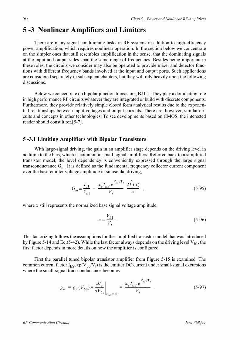
50 Chap.5 , Power and Nonlinear RF-Amplifiers
RF-Communication Circuits Jens Vidkjær
5 -3 Nonlinear Amplifiers and Limiters
There are many signal conditioning tasks in RF systems in addition to high-efficiencypower amplification, which requires nonlinear operation. In the section below we concentrateon the simpler ones that still resembles amplification in the sense, that the dominating signalsat the input and output sides span the same range of frequencies. Besides being important inthese roles, the circuits we consider may also be operated to provide mixer and detector func-tions with different frequency bands involved at the input and output ports. Such applicationsare considered separately in subsequent chapters, but they will rely heavily upon the followingdiscussions.
Below we concentrate on bipolar junction transistors, BJT’s. They play a dominating rolein high performance RF circuits whatever they are integrated or build with discrete components.Furthermore, they provide relatively simple closed form analytical results due to the exponen-tial relationships between input voltages and output currents. There are, however, similar cir-cuits and concepts in other technologies. To see developments based on CMOS, the interestedreader should consult ref.[5-7].
5 -3.1 Limiting Amplifiers with Bipolar Transistors
With large-signal driving, the gain in an amplifier stage depends on the driving level inaddition to the bias, which is common in small-signal amplifiers. Referred back to a simplifiedtransistor model, the level dependency is conveniently expressed through the large signaltransconductance Gm. It is defined as the fundamental frequency collector current componentover the base-emitter voltage amplitude in sinusoidal driving,
(5-95)
where x still represents the normalized base signal voltage amplitude,
(5-96)
This factorizing follows the assumptions for the simplified transistor model that was introducedby Figure 5-14 and Eq.(5-42). While the last factor always depends on the driving level Vb1, thefirst factor depends in more details on how the amplifier is configured.
First the parallel tuned bipolar transistor amplifier from Figure 5-15 is examined. Thecommon current factor IESexp(Vbo/Vt) is the emitter DC current under small-signal excursionswhere the small-signal transconductance becomes
(5-97)
GmIc1
Vb1--------
f IES eVb0 Vt
Vt-------------------------------
2I1ˆ x x
--------------- ,=
xVb1
Vt-------- .
gm gm Vb0 dIc
dVbe-----------
Vb1 0=
f IES e
Vb0 Vt
Vt------------------------------- .= =

5 -3 Nonlinear Amplifiers and Limiters 51
Jens Vidkjær
Inserting into Eq.(5-95) we get
(5-98)
so the bias dependency is expressed through the small-signal conductance, which here is gov-erned directly by the applied bias voltage. For a given Vb0, the large-signal transconductancegrows with the drive level from gm in proportion to 2Î1(x)/x. This is shown as the upper constantvoltage bias curve in Figure 5-44. The voltage gain in the parallel tuned amplifier grows accord-ingly until the transistor is forced into saturation, and the simplified transistor model ceases.This direction of gain regulation is commonly useless and even dangerous from a stability pointof view. It is an amplifier that reduces gain and limits the output signal when the drive level in-creases that is required for most practical purposes.
One principle for a limiting amplifier is illustrated by.Figure 5-45(a). A current generatorin the emitter terminal keeps the DC current constant while the fundamental frequency and allhigher harmonic current components are shunted to ground through the coupling capacitor CE.To keep the DC emitter current Ie0 constant and equal to IEE implies that the operation of thecurrent generator is to adjust the voltage across itself, VEE, so the mean base-emitter voltageVb0 compensate variations in drive level Vb1. Using the DC branch in Eq.(5-44), biasing is nowincluded with functional dependencies
(5-99)
The small-signal transconductance at x=0 is here given by gm=f IEE/Vt, so the large-signaltransconductance from Eq.(5-95) gets the form
Gm Gm Vb0 Vb1 gm Vb0 2I1
ˆ x x
---------------= = x Vb1 Vt ,=
Gmgm
1000
100
10
1
0 1 2 3 4 5 6 7 8 9 100.1
0.05
0.2
1
2
5
20
Constant Voltage Bias
Constant Current Bias
A:
x = Vb1 /Vt
Figure 5-44 Normalized large signal transconductance for non-saturating parallel-tuned BJT amplifiers with eitherconstant voltage, constant current, or resistor biasing.
Ie0 IEE IESeVb0 Vt
I0ˆ x = Vb0 IEE Vb1 Vt
IEE
IES I0ˆ x
----------------------
log= xVb1
Vt-------- .= =

52 Chap.5 , Power and Nonlinear RF-Amplifiers
RF-Communication Circuits Jens Vidkjær
(5-100)
The lower curve in Figure 5-44, which is denoted constant current bias, shows the ratio ofGm over the small-signal counterpart, gm(IEE). Clearly, the effective transconductance here hasthe desirable self-limiting shape.
Current biasing is a technique that is well suited for integration. Between full integrationand discrete designs, there are examples of receiver IC's that offer the current generator for bi-asing an external oscillator amplifier. However, in discrete designs or with minimum noise re-quirements, a decoupled emitter series resistance is often used instead. This is shown in Figure5-45(b) and it provides a gain control between the two extremes of either simple voltage bias orcurrent bias. To investigate this circuit and ensure a transconductance that decreases with thedrive level, we should again start solving for mean values, in particular Vb0, where the inputloop provides
(5-101)
Although the equation above always has one solution with respect to Vb0, if x and the oth-er circuit parameters are given, the solution cannot be expressed analytically, so we must resortto numerical methods. Suppose that Vb00 is a solution at small-signal biasing condition withx=0. The corresponding emitter DC current Ie00 and small-signal transconductance gm are relat-ed through,
(5-102)
+
Ic0Ic0
Ie0
IcIc
IbIb
VbeVbe
Vbe =Vb0+Vb1cosω0t
VEVE VBBVBB
REIEE CECE
C
( a ) ( b )
RLVL
VCC
Lchk
L
Ccpl Ic1cosω0t
Figure 5-45 Limiting tuned amplifier with either current (a) or resistor (b) biasing. Capacitor CE short-circuits bothfundamental and all higher harmonic current components.
Gm const.currentGm IEE Vb1 gm IEE
2I1ˆ x
xI0ˆ x
---------------= =gm IEE f IEE Vt ,=
x Vb1 Vt .=
VBB Vb0– VE REIe0 REIESeVb0 Vt
I0ˆ x = = = x Vb1 Vt .=
VBB Vb00– VE REIe00 VtREgmf
-------------= = =gm f Ie00 Vt ,=
Ie00 IESeVb00 Vt
.=

5 -3 Nonlinear Amplifiers and Limiters 53
Jens Vidkjær
Note, the x=0 solution corresponds to a conventional small-signal bias design, where VBB andRE are chosen to provide a required DC current. Often this solution is obtained assuming a fixedbase-emitter voltage of say 0.7V. Solved numerically, Eqs.(5-101) gives a more correct base-emitter DC voltages for any given base signal voltage Vb1. To formulate the numerical solutionprocess we first introduce Vb0, which is the change in the base-emitter DC voltage when a sig-nal is applied, into Eq.(5-101),
(5-103)
Normalizing by Vt and introducing Eq.(5-102), the last equation may be written in the form
(5-104)
where A is a constant that concentrates circuit parameters and z contains the unknown to besolved for
(5-105)
The procedure for obtaining normalized transconductance characteristics is to solve this equa-tion for the normalized bias voltage displacement z. The solution is considered as a function ofthe normalized drive level x with constant A being a parameter. When z is found numerically,we first express the leading bias controlled current factor through
(5-106)
We have here used the fact that Ie00 from Eq.(5-102) accounts for the initial bias voltage Vb00,while the exponential includes the bias voltage displacement when a drive signal is applied.Substituting Ie00 by the small-signal transconductance gm, the effective transconductance isagain calculated from Eq.(5-95), which now gives
(5-107)
Curves showing relative variations of the effective transconductances as functions of the drivelevel are included in Figure 5-44 for various settings of the A-parameter. It is seen that to get aneffective self limiting large signal transconductance, the product of the emitter series resistanceand the initial small-signal transconductance should be approximately five or more. It is implic-itly contained in the above computations that gain reduction is accompanied by an emitter DCcurrent growth from the small-signal value Ie00 to Ie0, where
(5-108)
Vb0 Vb00 Vb0+= VBB Vb00– Vb0– REIESeVb0 Vt
I0ˆ x e
Vb0 Vt .=
A z– AI0ˆ x ez ,=
AREgmf
------------- zVb0
Vt------------ .
z z x A = IESeVb0 Vt
Ie00ez .=
Gm resistor biasedGm Vb1 A gm
2I1ˆ x ez x A
x--------------------------------= = x Vb1 Vt .=
Ie0 IESeVb0 Vt
I0ˆ x Ie00ezI0
ˆ x .= =

54 Chap.5 , Power and Nonlinear RF-Amplifiers
RF-Communication Circuits Jens Vidkjær
Expressing large signal transconductance Gm by the approach above may be illuminatedby the block-scheme in Figure 5-46. The transistor is driven by a sinusoidal signal voltage Vb1with DC offset Vb0. The transistor model, which is expressed through Eq.(5-44), provides cor-responding fundamental frequency and DC current components. The latter is returned to makea signal level dependent bias change, which limits the gain. The purpose of the solution processabove is to eliminate the feed-back loop leaving alone only the fundamental frequency input-output relation, i.e. the large signal transconductance Gm. The present solution assumes station-arity because all equations are algebraic. Later we shall extend the technique, which in literatureis known as first harmonic or describing function analysis, to encompass dynamic behaviour ioscillator stability investigations.
If transistors are driven directly by voltage generators like the examples above, there is noneed to consider input impedances. The level of approximation that was introduced by Figure5-15 and the pertinent discussion on page 17, implies a purely resistive input impedance. Theassumption that the base current is a constant fraction of the emitter current - consequently alsoof the collector current - means that the fundamental frequency input impedance R1 is directlyrelated to the effective transconductance by
(5-109)
The equivalent circuit in Figure 5-47 describes the stationary large-signal operation of the tran-sistor including the different methods of biasing the emitter. A direct use of this diagram is tovisualize constraints among fundamental frequency currents and voltages. To employ the dia-gram successfully in a circuit schematic it is important that the circuit imposes proper filteringat the input side of the transistor, so the sinusoidal drive is guaranteed.
Transistor model(describing function)
( a ) ( b )
Vb1 Gm( Vb1| A )Ic1
Ic1
Ie0
Vb1
VBB
VE
×RE
Vb0
Figure 5-46 Block-scheme representation of the equations that express the large-signal transconductance Gm. Thetransistor model block contains Eq.(5-44) using n=0 and n=1.
Ic1 GmVb1 f Ib1= = RVb1
Ib1--------
fGm------- , where f
f1 f–-------------- .= = =
Ic1 Ic1Ib1
Ib1
Vb1
Vb1
Gm Vb1
R 1
= βf / Gm
Figure 5-47 Large-signal, fundamental frequency representation of a transistor with bypassed emitter resistor ofbypassed current source.G depends both on the DC bias and the signal level Vb1 as expressed throughthe curves in Figure 5-43.

5 -3 Nonlinear Amplifiers and Limiters 55
Jens Vidkjær
Example 5 -3-1 Limiting BJT Amplifier
The task is here to design an amplifier with resistor limiting like Figure 5-45(b), whichfulfils the following requirements,
- operating frequency, f0 = 10 MHz,- maximum input drive, Vb1 = 125 mVrms ~ 176.8 mVp,- output power at maximum drive, Pout = 20 mW,- gain reduction at maximum drive 1:3,- 3rd harmonic distortion at maximum drive < -46 dBc,- battery voltage, VCC=5 V,- transistor data, ßf= 60, IES=3.7fA,- minimum Vce to prevent saturation effects, Vce,min= 1 V.
The maximum drive specification gives directly
(5-110)
From Figure 5-17, mathematical tables, or mathematical programs the corresponding modifiedBessel functions, which are required below, become
(5-111)
With a known gain reduction, Eq.(5-107) provides a method for calculating the normalized dis-placement z in the base-emitter mean voltage, when a maximum signal is applied.
(5-112)
The A constant that controls the gain reduction was introduced by Eq.(5-104), which provides
(5-113)
From the definition of A we have
(5-114)
so the voltage across the emitter series resistance with maximum signal may be found from therelationships in Eqs.(5-101) through (5-104). They give
x xmaxVb1 p
Vt------------- 0.1768
0.025---------------- 7.071 .= = = =
I0ˆ xmax 180.06= I1
ˆ xmax 166.79= I3ˆ xmax 91.622 .=
Gmgm------- 1
3---
2I1ˆ xmax ez
xmax----------------------------= = ez
xmax
6I1ˆ xmax
----------------------- 7.0716 166.8--------------------- 7.066 10
3–= = =
zVb0
Vt------------
7.066 103– log 4.954 .–= =
A z– AezI0ˆ xmax A 7.066 10
3–180.06 A 1.2723= = =
A
z–1.2732 1–------------------------- 4.954
0.2723---------------- 18.19 .= = =
AREgmf
-------------REIe00
Vt--------------- ,=

56 Chap.5 , Power and Nonlinear RF-Amplifiers
RF-Communication Circuits Jens Vidkjær
(5-115)
The maximum output voltage amplitude VL1 is illustrated in Figure 5-47. It is bounded by therequirement of avoiding saturation effects and of making room for the emitter resistor voltage.It becomes
(5-116)
With this output voltage swing, the required output power determines the fundamental frequen-cy output current amplitude and the corresponding load resistance,
(5-117)
(5-118)
The ratio of the emitter fundamental frequency current component over the DC current is theratio of two times the 1st order modified Bessel function over the zero order function. Adjustingfor the small base current, which is expressed through the current gain factor
(5-119)
the emitter mean current with applied signal becomes,
VE VBB Vb0– REIe0 RE Ie00ezI0ˆ xmax Vt AezI0
ˆ xmax
0.025 18.19 1.272 0.5786 V .= = = =
= =
0V 0 2
( a ) ( b )
Vbe=Vb0+Vb1cosω0t
Vce,min + VEEVBB
VCC = 5V
VCC
VE RE
CE
Ccpl
Lchk
RLC L
Vbe
Ic0
Vce
Vc
Vc
VL
VL1
ZL(ω )
ωt
Figure 5-48 Self-limiting BJT amplifier diagram (a) and output voltage conditions (b).
VL1 VCC Vce min– VE– 5.0 1– 0– 0.5786– 3.421 Vp .= = =
PoutVL1Ic1
2----------------= Ic1
2PoutVL1
------------- 2 203.421------------- 11.69 mA ,= = =
RLVL1
Ic1-------- 3.421
0.01169------------------- 292.7 .= = =
ff
f 1+-------------- 60
61------ 0.9836 ,= = =

5 -3 Nonlinear Amplifiers and Limiters 57
Jens Vidkjær
(5-120)
The emitter mean current before the signal is applied, Ie00, is found through Eqs.(5-108),
(5-121)
and the corresponding base-emitter mean voltage without input signal is,
(5-122)
From the definition of the A constant we get
(5-123)
One method of finding the base battery voltage is to express the mean voltages around the inputloop if no signal is applied,
(5-124)
Alternatively, and as a consistency check of the results above, we may conduct a similar calcu-lation when the signal is applied. Here the mean base-emitter voltage becomes
(5-125)
which, when added to the emitter voltage from Eq.(5-115), gives
(5-126)
As seen, this is the same base bias that was found by Eq.(5-124).
It is supposed that the collector bias choke Lchk is large enough to force all harmonic cur-rent components through the loading resonance circuit, L, C, and RL. Then, the ratio of the thirdharmonic over the fundamental frequency output voltage components may be expressed interms of the load impedances at these frequencies by
(5-127)
Ie0Ic1 I0
ˆ xmax
f 2 I1ˆ xmax
-------------------------------- 11.69 180.10.9836 2 188.8 ------------------------------------------ 6.415 mA .= = =
Ie00 IESeVb0 Vt Ie0
ez I0ˆ x
------------------ 6.4151.272------------- 5.042 mA ,= = = =
Vb00 VtIe00
IES-------- log 0.025
5.042 103–
3.7 1015–
----------------------------
log 0.699 V .= = =
ARE gmf
-------------- REIe00
Vt--------= = RE
AVtIe00--------- 18.19 25.0
5.042---------------------------- 90.19 .= = =
VBB Vb00 RE Ie00+ 0.6985 90.19 5.042 103– + 1.153 V .= = =
Vbo Vb00 Vb0+ Vb00 zVt+ 0.6985 4.953 0.025– 0.5747 V ,= = = =
VBB Vb0 VE+ 0.5747 0.5786+ 1.153 V .= = =
VL3
VL1--------
ZL 30 ZL 0
--------------------------I3ˆ xmax
I1ˆ xmax -------------------- .=

58 Chap.5 , Power and Nonlinear RF-Amplifiers
RF-Communication Circuits Jens Vidkjær
The size of the load impedance at the fundamental and at the third harmonic frequencies are giv-en through Eq.II-(6),
(5-128)
Inserting these expressions into the voltage ratio from Eq.(5-127) gives the condition for findingthe Q-factor of the load, which is required to fulfil distortion requirements. We get
(5-129)
which implies a smallest Q-factor of
(5-130)
Choosing the Q-factor, the tuning components in the output resonance circuit become
(5-131)
To complete the design, biasing, coupling, and decoupling components must be fixed.Since the DC bias at the transistor input depends on the driving level, the emitter decouplingcapacitor determines how swiftly the gain tracks changes of the input signal. This aspect is cru-cial if the amplifier is employed by an oscillator coupling and will be discussed later in ExampleVI-1. A useful criterion is to set the gain regulating time constant equal to the time constant forvoltage amplitude changes across the tuning circuit in response to current changes. As demon-strated earlier in Chap.II, Figure II-9 this is the so-called logarithmic decrement. We get
(5-132)
At the output side there is no change of DC bias, so the primary concerns regarding bias chokeLchk and coupling capacitor Ccpl are that they should be chosen not to influence the tuning andloading conditions at the operating frequency, for instance
(5-133)
ZL 0 ZL 0 RL= = ZL 30 RL
1 jQ 3 13---–
+
--------------------------------------RL
1 Q22.667
2+
-------------------------------------= =
VL3
VL1--------
I3ˆ xmax
1 Q22.667
2+ I1
ˆ xmax ---------------------------------------------------------------=
1
1046 20
------------------ 1199.5------------- 46 dB –=
Q22.667
2 199.5I3ˆ xmax
I1ˆ xmax
----------------------------------2
1–199.5 91.62
166.7-------------------------------
2
109.62 ,=
Q 109.62.667------------- 41.10 .= =
Q 0CRL= C Q0RL------------- 41.10
2107
--------------- 2.235 nF = = =
L
1
02C
---------- 1
4210
142.235 10
9– --------------------------------------------------------- 113.3 nH .= = =
E RECE2Q0-------= = CE
2CRLRE
-------------- 2 2.235 109–
292.6 90.18
------------------------------------------------------ 14.59 nF .= = =
Lchk 10 H = L» 113.3 nH ,=

5 -3 Nonlinear Amplifiers and Limiters 59
Jens Vidkjær
(5-134)
Figure 5-49 shows a simulation of the output from the amplifier that has the components abovewhen a maximum signal of Vb1=125 mVrms is applied instantly at time = 1sec. Even thoughthe voltage gain in the whole transient period is larger than the resultant, reduced voltage gain of
(5-135)
the criterion for CE in Eq.(5-132) implies no output voltage overshoot before settlement.
Example 5 -3-1 end
5 -3.2 Limiting with Bipolar Differential Amplifiers
A distinct way of employing current bias is to use a differential amplifier stage as a lim-iting amplifier. The differential pair principle in Figure 5-50 has an ideal current source IET forcurrent biasing. The subscript “T” stands for tail10 and this bias current is sometimes called thetail current. The input signal is balanced through a transformer that inserts DC bias trough thecenter tap in the secondary winding. This arrangement is not always the most suitable in practicebut it is employed here because it comes close to the ideal requirement in a simple analysis. Withcurrent biasing the base-emitter voltages at the two transistors are
(5-136)
The common DC component Vb0 is implied through the current bias, which is adjusted auto-matically so the sum of the currents through the two transistors becomes the bias current IET. We get
10. The differential amplifier stage was once called a "long-tailed pair".
10Ccpl----------------- RL« Ccpl 5 nF 1
0RL-------------» 54.7 pF .= =
-4
-2
0
2
4
[ μsec ]0. 2. 4. 6. 8. 10.
VL [V]
Figure 5-49 Output voltage transient in the amplifier from Figure 5-48(a) with a maximum input signal appliedinstantly at time equal to 1sec.
AV Vb1 max VL1
Vb1 max------------------ 3.421
0.1768---------------- 19.35 ,= = =
V1be Vb0
Vid t 2
---------------+= V2be Vb0
Vid t 2
--------------- .–=

60 Chap.5 , Power and Nonlinear RF-Amplifiers
RF-Communication Circuits Jens Vidkjær
(5-137)
A differential output voltage from the amplifier can be established by ohmic loading as is it wasdone in Figure 5-50. In tuned amplifiers the output is taken either directly or through a trans-former as sketched in Figure 5-51 (a) and (b). It is the difference between the two collector cur-rents that controls the differential output in all cases. This difference is most convenientlydefined as the deviation Ic from the bias currents, which - as indicated by Figure 5-50 - circu-lates through both transistors and both load resistors,
(5-138)
The expressions in the last line is obtained by substitution with the last expression from Eq.(5-137). Introducing the normalized drive voltage x like it was done before with a single BJT tran-sistor amplifier, the result above may also be written
(5-139)
0V0V
VCC
VEE
V2beV1be I1e I2eVid /2
Vid /2
∆Ic
Vout= 2RL∆Ic
RLRL
IET
I2c= Ic0 - ∆IcI1c= Ic0 + ∆Ic
I1b= Ib0 + ∆Ib
I2b= Ib0 - ∆Ib
B2B1
C1 C2
Q1 Q2
Figure 5-50 Differential amplifier principle
I1e IES eVb0 Vt
eVid t 2Vt
= I2e IES eVb0 Vt
eVid t 2Vt–
=
IET
I1e I2e+ IES eVb0 Vt e
Vid t 2Vte
Vid t 2Vt–+ . = =
Ic12--- I1c I2c–
f2----- I1e I2e–
f IES2
-------------- eVb0 Vt
eVid t 2Vt
eVid t 2Vt–
–
f IET2
--------------e
Vid t 2Vte
Vid t 2Vt––
eVid t 2Vt
eVid t 2Vt–
+ --------------------------------------------------------------
f IET2
--------------Vid t
2Vt-------------- .tanh
= = =
= =
Icf IET
2-------------- x
2--- tanh= x
Vid t Vt
-------------- .=
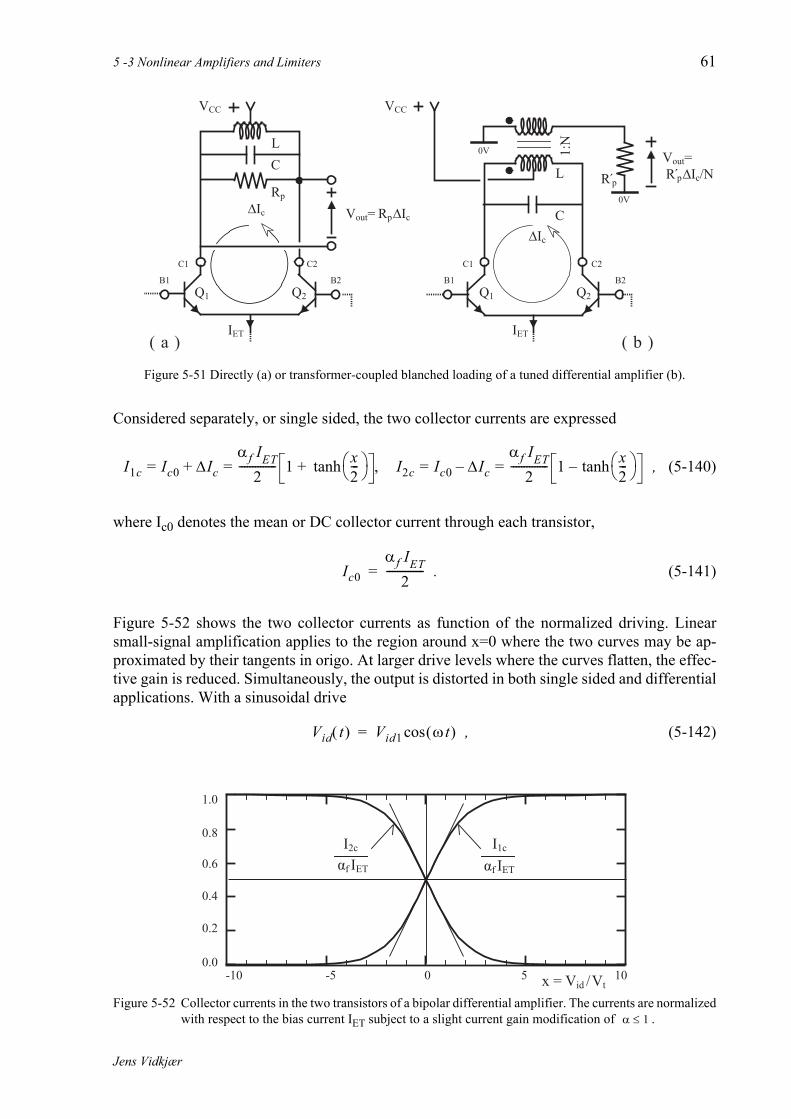
5 -3 Nonlinear Amplifiers and Limiters 61
Jens Vidkjær
Considered separately, or single sided, the two collector currents are expressed
(5-140)
where Ic0 denotes the mean or DC collector current through each transistor,
(5-141)
Figure 5-52 shows the two collector currents as function of the normalized driving. Linearsmall-signal amplification applies to the region around x=0 where the two curves may be ap-proximated by their tangents in origo. At larger drive levels where the curves flatten, the effec-tive gain is reduced. Simultaneously, the output is distorted in both single sided and differentialapplications. With a sinusoidal drive
(5-142)
C
L
C
L
( a ) ( b )
1:N
0V
0V
VCC
Rp
R p
VCC
∆Ic
∆Ic
B2B1
C1 C2
Q1 Q2
B2B1
C1 C2
Q1 Q2
Vout= Rp∆Ic
Vout= R p∆Ic/N
IETIET
Figure 5-51 Directly (a) or transformer-coupled blanched loading of a tuned differential amplifier (b).
I1c Ic0 Ic+f IET
2-------------- 1
x2--- tanh+= = I2c Ic0 Ic–
f IET2
-------------- 1x2--- tanh– ,= =
Ic0
f IET2
-------------- .=
0.00-5 5-10 10
0.2
0.4
0.6
0.8
1.0
I2c
x = Vid /Vt
I1c
αf IETαf IET
Figure 5-52 Collector currents in the two transistors of a bipolar differential amplifier. The currents are normalizedwith respect to the bias current IET subject to a slight current gain modification of . 1
Vid t Vid1 t ,cos=

62 Chap.5 , Power and Nonlinear RF-Amplifiers
RF-Communication Circuits Jens Vidkjær
the differential current, which has no DC component, is given by a Fourier series that - due tothe symmetry of the hyperbolic tangent function - contains only odd components,
(5-143)
There are no analytical expressions for the integrals. Harmonic components of first, third andfifth order are evaluated numerically and shown in Figure 5-53. The differential large-signaltransconductance Gmd is derived from the first harmonic component according to
(5-144)
where gmd denotes the small-signal differential transconductance. It is given by
(5-145)
The fully drawn curve in Figure 5-54 shows how the large-signal transconductance, taken rela-tive to gmd, depends on the driving level. It is readily seen that the differential amplifier stage isusable as a limiting amplifier as the gain reduces distinct and smoothly with increasing inputvoltage level.
Ic Icn nt cos
n 1=
n odd
f IET
2-------------- an x nt cos
n 1=
n odd
= =
an x
1--- x
2--- t cos tanh nt cos td
–
= xVid1
Vt---------- .=
10 15 2050
0.2
0.4
0.6
0.8
1.0
1.2
1.4
0.0
-0.2
-0.4
-0.6
1.273
0.255
-0.424
a1(x)
a5(x)
a3(x)
x = Vid /Vt
Figure 5-53 Fourier coefficients of 1st, 2nd, and 3rd order for the normalized differential current in a bipolar dif-ferential amplifier. The dotted asymptotes are the Fourier coefficients of an ideal square-wave.
GmdIc1
Vid1----------
f IET2Vt
--------------a1 x
x------------- gmd
2a1 x x
---------------- ,= = =
gmdd Ic1
d Vid1--------------
Vid1 Vt«
f IET
2-------------- 1
Vid1
2Vt----------
2tanh–
12Vt--------
Vid1 Vt«
f IET4Vt
-------------- .= =

5 -3 Nonlinear Amplifiers and Limiters 63
Jens Vidkjær
Driven by large input signals, the transistor currents in the differential amplifier will moreand more resemble an ideal square-wave as shown in Figure 5-55 (d). A step towards this limitis illuminated in Figure 5-55 (a-c), which show driving conditions for one of the transistors, Q1.The limiting square-wave current I1c,sq in the transistor is described by the Fourier expansion
(5-146)
(5-147)
10 15 2050 x = Vid /Vt
Gmd /gmd
0.2
0.4
0.6
0.8
1.0
0.0
Figure 5-54 Normalized large-signal differential transconductance for a bipolar differential amplifier. The dottedcurve indicates the transconductance of an ideal limiter given by Eq.(5-148).
fundamentalfrequency component
fundamentalfrequency component
( a )
( b ) ( c )
( d )
ωt
ωtωt
Vid
Vid
I1c,lim
Ic0
Ic0
I1cI1c
Figure 5-55 Operation of one transistor in a bipolar differential amplifier. An input voltage corresponding tox=5(a) is applied to the transfer characteristic (b) and produces the fully drawn output current in (c).The square-wave current in (d) corresponds an infinitely large x.
I1c sq Ic0 Ic sq+= Ic sq Ic0 qn nt ,cos
n 1=
n odd
=
qn 1– n 1–
2------------ 4
n------= n 1 3 5 . =

64 Chap.5 , Power and Nonlinear RF-Amplifiers
RF-Communication Circuits Jens Vidkjær
which applies to a symmetrical square wave function between 1 and -1. The numerical valuesof the first three Fourier coefficients were indicated by the horizontal asymptotes in Figure 5-53. If the bias current is kept fixed, the differential current will approach a fixed amplitude ofIc0, which has a fundamental frequency component of amplitude q1Ic0. Approaching a constantoutput current while the driving voltages grows means that the transconductance more and morebecomes inversely proportional to the driving voltage
(5-148)
This expression is inserted as the dotted curve in Figure 5-54, where it is seen that from 10 andup in x=Vid1/Vt, the differential stage comes close to an ideal or hard limiter since it closely fol-lows the asymptotic relationship above.
The differential circuit has the advantage that the limiting function occurs when the tran-sistors run out of current. It does not require saturation or avalanching in diodes and other junc-tions, functions that are accompanied by excessive carrier storage and consequently limits theoperating frequency. To maintain this advantage, the transistors must clearly be prevented frombecoming saturated. If we suppose ideal output characteristic of the type that was introduced byFigure 5-15 (c), where saturation is avoided if Vce stays positive, the bias and load lines mustbe organized as shown in Figure 5-56. The first, squared output voltage corresponds to the ohm-ic loading in Figure 5-50 and requires
(5-149)
Here, the adjustment in voltage range is introduced because it is the base that is biased to zero.It is from the base there is the voltage across the conducting emitter diode down to the emitterpotential, Ve0, which is assumed constant, equal to -0.6 Volt.
Gmd x Gmd
q1Ic0
Vd1------------
f IET2Vt
--------------q1
x----- gmd
8x------ .= = = =
slope: -1/RL,max slope: -1/Rp,max
( a ) ( b ) ( c )
I1c I1c
αf IET αf IET
I1c
VceVCC -Ve0 VCC -Ve0
Vce
Vce
Vce
ωt ωt
Figure 5-56 Loading conditions for unsaturated operation of each transistor in a bipolar differential amplifier if itis driven by a large input (Q1 is the example here). The outputs correspond to ohmic loading (b) likeFigure 5-50, or tuned loading (c) by one of the methods in Figure 5-51.
RL RL maxVCC Ve0–
f IET------------------------
VCC 0.6V+
IET---------------------------- .=

5 -3 Nonlinear Amplifiers and Limiters 65
Jens Vidkjær
In the case of tuned loading by the methods in Figure 5-51, it should be kept in mind thatit is the fundamental frequency current component that drives the load. This component exceedsthe bias current by a factor up to q1=4/ in case of hard saturation. Leaving room for the corre-sponding voltage swing provides now the maximum parallel load resistance
(5-150)
in accordance with the sketch in Figure 5-56 (c).
Assuming that the base currents are constant fractions of the corresponding emitter or col-lector currents in the transistors, the base currents under sinusoidal drive become
(5-151)
Similar to the single transistor amplifier case, the fundamental frequency input impedance issupposed to be resistive and related to the differential transconductance through,
(5-152)
where f and f are related by
(5-153)
A circuit representation constraining fundamental frequency components is shown in Figure 5-57. Like its single transistor stage counterpart in Figure 5-47, the input drive must be sinusoidal,so filtering is required at the input port if the input generator is not sinusoidal or if it has a gen-erator impedance of significance being comparable to or greater that Rin1.
q1Ic0
Rp2
------ VCC Ve0– Rp Rp max4 VCC Ve0–
q1f IET--------------------------------
VCC 0.6V+ IET
-------------------------------- ,=
I1b Ib0 Ib ,+=
I2b Ib0 Ib ,–= where Ib0 1 f–
IET2
-------= ,
Ib Ib1 t cos= .
Ib1
Ic1
f----------
GmdVid1
f--------------------= = Rin1
Vid1
Ib1-----------
fGmd---------- ,= =
ff
1 f–-------------- or f
ff 1+-------------- .= =
B1
B2
C1
C2
Vid1Rin1 = ßf /Gmd GmdVid1
∆Ic1∆Ib1
Figure 5-57 Differential, fundamental frequency equivalent circuit for a differential amplifier

66 Chap.5 , Power and Nonlinear RF-Amplifiers
RF-Communication Circuits Jens Vidkjær
Chap.5, References and Supplementary Literature
[5-1] S.C.Cripps, RF Power Amplifiers for Wireless Communications, Artech House,1999.
[5-2] S.C.Cripps, Advanced Techniques in RF Power Amplifier Design, Artech House,2002.
[5-3] M.A.Ambromowitz, I.A.Stegun, Handbook of Mathematical Functions, Dover,1965.
[5-4] N.E.Dye, "Understanding RF Data Sheet Parameters" Freescale (Motorola) Applica-tion Note AN1107.
[5-5] A.Wood,B.Davidson,"RF Power Device Impedances, Practical Considerations",Freescale (Motorola) Application Note AN1526.
[5-6] J.Vidkjaer”A Describing Function Approach to Bipolar RF-Power Amplifier Simu-lation”, IEEE Trans. Circuit and Systems, vol.CAS-28, No.8 Aug.1981, pp-758-767.
[5-7] T.H.Lee, The Design of CMOS Radio-Frequency Integrated Circuits, CambridgeUniversity Press, 1998.

5 -3 Nonlinear Amplifiers and Limiters 67
Jens Vidkjær
Chap.5, Problems
P 5.1 The amplifier circuit in Figure 5-58 (a) compensates for transistor gain variation bythe RS, CS combination in the source at the expense of output power and efficiency.The capacitor is supposed to short circuit all source ac-current components. CL is acoupling capacitor to the load. The transistor is modelled by the simplified character-istic and equivalent circuit in Figure 5-58 (b). The output power in RL' must be 10Wat 75 MHz when the transistor is driven to the peak current and with maximum un-distorted voltage swing. The minimum drain-source voltage Vdsmin, and the DC-volt-age VRS must stay above 0.5V and 2.0V respectively.
Find the fundamental frequency components of the drain current, Id1, and the outputvoltage,Vo1. Determine the load resistor RL' and the conduction angle.
Calculate the required gate drive and bias voltages Vg1, VGG, the source resistanceRS. What is the efficiency of the amplifier?
Load resistor RL' represents a converted antenna impedance RL = 300 Ohm. Thetransformation is made by the circuit in Figure 5-59, where CL still is a coupling ca-pacitor. Determine Cp and Ls.
0V 2V
2A
5V
s
g d
( a ) ( b )
VDD= 24V
C p
CL
RS CS
L p
Id
Id
Id
Id,maxVds
Vgs
Vo
VRS
VGG
Vg1cosω0t
Figure 5-58
25nH
300Ω
VDD
Lp Cp
CL
RL
Ls
Figure 5-59

68 Chap.5 , Power and Nonlinear RF-Amplifiers
RF-Communication Circuits Jens Vidkjær
P 5.2 The differential amplifier in Figure 5-60 is operated with an unbalanced load. Atmaximum sinusoidal input level vd =VDcos0t, it should be driven to a voltage gainthat is 1/3 of its small signal gain. Furthermore, the amplifier should be operated withmaximum undistorted output, i.e. to the limit of Vce = 0 in transistor Q2.
Find the bias current IET, the small signal transconductance gmd, and the center fre-quency voltage gain A=Vout/VD using RL=1.2 kOhm and VCC=5V.
Calculate the 3rd to 5th order contributions to the total harmonic distortion of the out-put voltage if the loading circuit has a Q-factor of 100.
0V
Vd
IET
Ic2
VCC
Vout
RL
Cp
Ccpl
Lp
Q1 Q2
Figure 5-60

69
Jens Vidkjær
INDEX BBreak-Point Characteristic ...................2, 6
CClass A Amplifier ..............................5, 10Class AB Amplifier ...............................10Class B Amplifier ..................................10Class C Amplifier ..................................10Class E Amplifier ..................................37
"optimal" ....................................37, 42Conduction Angle (in parallel tuning) .....6
bipolar (BJT) approximation ...........19
DDescribing Function Analysis ...............54
EEfficiency ................................................3
battery ................................................3collector .............................................3drain ...................................................3in class A amplifiers ..........................5in prototype amplifiers ....9, 11, 16, 22in series tuning ...........................36, 37power added .......................................3simple ................................................3
Encapsulation ComponentsMOSFET example ...........................32
FFirst Harmonic Analysis ........................54
LLarge Signal Transconductance
in differential BJT amplifiers .......... 62in single BJT amplifiers ...... 50, 51, 53
Limiting Amplifiersdifferential BJT ............................... 59ideal or hard ..................................... 64single BJT ........................................ 50
Long Tailed Pair .................................... 59
MModified Bessel Functions .............. 18, 19
PPeak Envelope Power ............................ 28Prototype Amplifier
parallel tuned ..................................... 2
RRF-Power Amplifier
bipolar, BJT ..................................... 16MOSFET ......................................... 23parallel tuned ..................................... 2prototype ............................................ 2series tuned ...................................... 32square-law FET ............................... 13
SSeries Tuned Power Amplifiers ............ 32Switch Opening Angle (series tuning) .. 34
TTwo-Tone Test ...................................... 28

70 ,
RF-Communication Circuits Jens Vidkjær