rf control products training module
TRANSCRIPT

MARKET TRAINING MODULE
RF Control Products

2
List of Content
Introduction RF Switches RF Attenuators

3
Introduction
Control Products are defined as impacting the signal chain performance By configuring the Chain By adjusting the signal level NOT amplifying or converting the signal (i.e. ideally linear and passive) Operating Frequency above 1GHz to close to 100GHz
RF Switches (SPST, SPDT, SP3T, SP4T, etc.) RF Attenuators (Digital, i.e. DAT, Analog) TX/RX Switches
15dB
24dB
9dB
1.9-
2.34
GH
z
1.25-1.8GHz
1.8-2.5GHz
870-1250MHz
2.5-3.4GHz
600-870MHz
450-600MHz
3.4-5GHz
10-450MHz
1768
2500
1250
3536
884
625a
5000
625b

4
Application and Marketing Considerations
ALL RF Systems/PCB include RF Switches and often RF Attenuators Some systems (PCB) have 30 to 50 RF switches and few attenuators Examples:
Inserting a calibration signal in the Signal Chain Bypassing fixed-gain amplifiers Routing a signal to different (frequencies) downconversion chains Routing an LO signal thru alternative frequency selective gains, before the
mixer Optimizing the RF signal level for best noise performance, after a fixed gain
stage (LNA) or between fixed gain stages

5
RF Control Product: Common Basic Knowledge
RF Devices, packaged for PCB usage RF “Connectorized” Components, to be used as stand alone Passive, i.e. always have a transfer attenuation
RF Switches key function is to route Signals to different Signal Chains RF Attenuators key function is to maintain the RF Signal Levels to the
planned ranges for best system performance
Controlled Signals are Information signal (receive, transmit) Clocks, Local Oscillators

RF Switches

7
RF Switches: Naming
Single Pole Single Throw (SPST)
Single Pole Dual Throw (SPDT)
Single Pole “X” Throw (SPXT)
Notes Double Pole (e.g. in a DPDT) normally called “Differential” RF circuits are normally single ended
(Ex: SP8T)
8
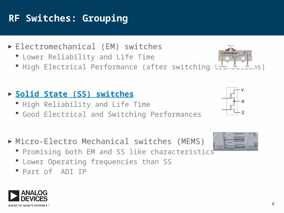
RF Switches: Grouping
Electromechanical (EM) switches Lower Reliability and Life Time High Electrical Performance (after switching transitions)
Solid State (SS) switches High Reliability and Life Time Good Electrical and Switching Performances
Micro-Electro Mechanical switches (MEMS) Promising both EM and SS like characteristics Lower Operating frequencies than SS Part of ADI IP

9
RF Solid State Switches: technological options
FET-based switches GaAs – Fast, High Frequency capability (100Hz), less robust (ESD) Silicon – getting faster, good settling time, med Frequency (20-40GHz), robust
Pin Diode switches High frequency (100GHz), robust, difficult to drive/control
Hybrid (FET and Pin Diode) Combination of both the above May not allow a monolithic solution
10
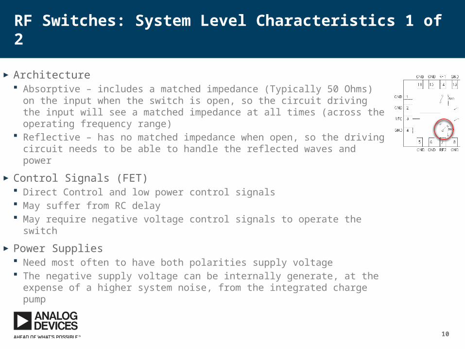
RF Switches: System Level Characteristics 1 of 2
Architecture Absorptive – includes a matched impedance (Typically 50 Ohms) on the
input when the switch is open, so the circuit driving the input will see a matched impedance at all times (across the operating frequency range)
Reflective – has no matched impedance when open, so the driving circuit needs to be able to handle the reflected waves and power
Control Signals (FET) Direct Control and low power control signals May suffer from RC delay May require negative voltage control signals to operate the switch
Power Supplies Need most often to have both polarities supply voltage The negative supply voltage can be internally generate, at the expense
of a higher system noise, from the integrated charge pump

11
RF Switches: System Level Characteristics 2 of 2
DC coupling ALL Traditional RF switches do not like DC signal through them DC decoupling caps are needed, unless a 0Vdc can be guaranteed Decoupling Caps will impact the low frequency performance New Technology in development with DC handling capability
Power consumption Low static power consumption (100-300uA)
Reliability (SS) Highest among available technologies GaAs switches have low ESD threshold, requiring specific care

12
RF Switches: Electrical Characteristics
Frequency Range (from 1-2GHz to 80GHz+) Insertion Loss (normally lower than 0.5dB, or max 1dB) Return Loss (normally higher than 10-15dB) Power Handling (the higher the better, now around 30dBm, moving to
40dBm+) Isolation (normally in the 25-50dB, frequency dependent) Distortion/Linearity (normally high, above 50dBm) Switching Speed (from 10ns to 1us depending on used processed, GaAs
is faster, Si is slower) Settling Time (from 100ns to 5us depending on the fabrication process
used, Si is slower, but has a shorter settling time) Noise (Leakage, switching)

13
Operating Frequency Range – Insertion Loss (IL), Return Loss (RL) Frequency Range is commonly the FIRST selection criteria for
switches
Insertion Loss is mostly impacted by The switch’s direct intrinsic resistance Reflected Loss as of the switch resistance Leakage paths, which reduce the useful signal power to the load IL must be compensated for by other circuits or taken into account
when performing level planning (as it impacts noise performance)
Frequency dependent IL Low Frequency IL is affected by
Any decoupling Cap at the In/Out leads Power handling (see later) capability
High Frequency IL is affected by Intrinsic parasitic capacitances
In band IL variation is affected by Return Loss, caused by impedance mismatching
Return Loss (RL) Indicates the amount of power not transferred over the switch (but
reflected back) Depends on the impedance matching (50OHM) of the switch with the
externally connected devices
Note: PIN diode switches do not normally operate well at low frequency. They excel at high frequencies (60GHz and above).
Return Loss
Insertion Loss

14
Signal Power Handling and Distortion
Switch capability to handle high power signals Allows to deploy switches closer to the system RF
connectors Decreases at lower frequencies, as limited by process
technology and switch architecture Defined while the switch is static or switching (Hot
switching power) Described by P1dB (or PSAT)
Distortion Measured by IP3 Related with Power handling
Approaching P1dB non linearity increases (IP3 decreases) Normally the Switch is not the critical Signal Chain block
on distortion Power De-rating compared to therequired nominal powerthe switch can operate at
IP3Decrease at low frequencies
15
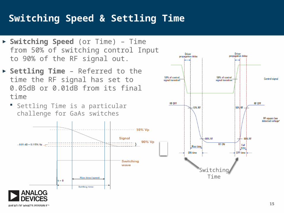
Switching Speed & Settling Time
Switching Speed (or Time) – Time from 50% of switching control Input to 90% of the RF signal out.
Settling Time – Referred to the time the RF signal has set to 0.05dB or 0.01dB from its final time Settling Time is a particular challenge for GaAs
switches
SwitchingTime

16
Isolation
Signal going through the switch when it is OFF From the common I/O to any other port Between two different ports
Normally NOT the coupled noise from the control ports (see later)
FET switches have very high low frequency isolation Drain-Source Cap is limiting high frequency
isolation This can be improved by shunting the input port to
ground when the switch is open (implemented inside the switch itself)
Pin Diode Switches have good high-frequency isolation (and poor isolation at low frequencies)
RF1
RF2
RFC

17
Other Noise and Sources of Interference
Video leakage or feedthrough Describes the noise from the control ports to the
RF ports Normally measured when no RF is present
(reported in mV) Lower in FET switches Critical is some applications (for example when a
high gain AGC amplifier follows the switch)
Power Supply Noise From external supplies – to be managed by proper
filtering From internal bias voltages (normally negative)
generated by an integrated charge pump Typically avoided by high end applications (T&M)

18
RF Switches - Application Topics
RF Ports Coupling - Traditional RF switches are not taking any DC signal Requiring DC decoupling at the ports. Impacting the IL at low frequencies. Proper selections of the Caps would depended on the desired low
frequency performances. Decoupling Caps can be avoided if the operating signals have no DC component (this is mentioned
often in datasheets as “not needing any decoupling Cap”!!!)
Power Supplies Switches can operate from single supply or from dual supplies A competitor has integrated the Vneg supply, with the related system noise drawback
Power Handling A critical system parameter, in many application, as the switch might need to be protected, especially
at low frequencies (below 10-100MHz) Improved handling is achieve with Si based switches
Control Signals – voltage ranges, drive Control voltage polarity depends on the switch supplies, and can be also negative voltages Latest switches operate with positive voltages (compatible with standard logic levels), and have bipolar
supplies Solid state switches are easy to drive (unlike some PIN Diode based switches)

RF Attenuators

20
RF Attenuator Typicales
Fixed Attenuators (“Pads”)
Digitally-Controlled Attenuators (DAT) Serial or parallel Control Series of switched-in/out fixed attenuators Resolution from 1bit to 7bit
Analog (Voltage) Controlled Attenuators (VVA) More complex control architecture Preferred when in AGC loops or for high signal
level accuracy

21
RF Attenuators: WHY?
Key justification for Attenuators Achieve a more optimized signal level plan (for noise and distortion)
RF amplifiers have commonly fixed gain RF amplifiers may not like high power input signals
G GA A
Input range Pin:From Pout-G+ATo Pout-G
Desired OutputRange: Pout
Signal Chain SNR Improved by G-NF-IL
Max PinMax Pin=Pin+A

22
RF Attenuators: Main and Common to the RF switches Electrical Characteristics Frequency Range: Operating Frequency Range
Attenuation Range: discrete or continuous
Attenuation Resolution (DAT): minimum nominal attenuation step, in dB. Related to the bit count and Attenuation Range E.G., 32dB range, 6 control bits (64 levels) gives 0.5dB resolution, to a max attenuation of 31.5dB (0dB attenuation included)
Attenuation Accuracy: nominal accuracy. Normally reported across frequency and attenuation range
Insertion Loss: Attenuation across the device, when 0dB is selected (ideally no attenuation applied)
Return Loss: reflected Power at the Input/Output ports, related to the device impedance matching
Power Handling (P1dB, P0.1dB): maximum input signal power, the device can handle and keep operating linearly. Normally reported across the frequency range.
Distortion/Linearity (IIP3): see RF Switch description, normally reported across the attenuation range
Switching Speed: see RF Switch description
Settling Time: see RF Switch description, normally reported across the attenuation range
Overshoot Free DAT: the Attenuator output presents no overshooting voltage, when switching between any attenuation steps, as a consequence of how the internal attenuation switches are operated
Power Supplies, Control Voltages: see RF Switch description
23
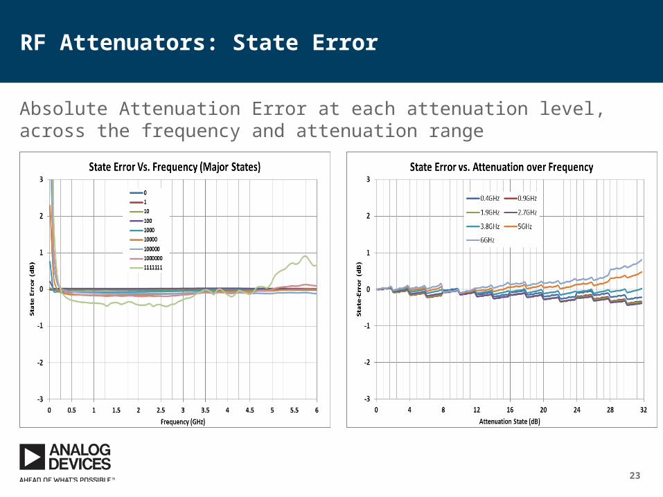
RF Attenuators: State Error
Absolute Attenuation Error at each attenuation level, across the frequency and attenuation range

24
RF Attenuators: Step Error
Relative Attenuation Error at each attenuation level, across the frequency and attenuation range

25
RF Attenuators: Phase Variation
Relative Phase variation from the output to the input signal, as it goes through the different internal attenuation steps
Normally reported as max value, across the frequency and attenuation range Also reported as graph

26
Analog Attenuators (VVA)
• Similar Function as with VGA, but implemented with an Attenuator (as “programmable wideband RF Amplifiers are rare”).
• Key technical challenges• Maintain Insertion Loss and Return Loss
performances in the attenuation range, across frequency range
• Linear relationship with the control voltages• Simplify control circuitry
Reference Attenuator Circuit
Discrete Control CircuitPlease see Ref.4 from the Reference List

27
Application Examples

28
LO Generation
LPF
LPF
LPF
SP3T
Test In
LOFout
SP4T
• Remove Spurious and Harmonics• High Insertion loss (6dB+)• Could be Band Pass on selected
Paths
Brings LO level to Max allowedAnd desired by the follow-onCircuit (eg mixer)
• Amplifies Fout• Isolates Fout from downchain• May be omitted, with certain Fout
Critical Parameters• Low insertion Loss• High Return Loss• High Linearity
End Application Dependent• Low video Leakage• Fast Switching/Settling• Power Handling
Non Critical Parameters• Isolation

29
RF Input Stage
DAT
G1
G2LNA
IL, RL impacts SNR Sets the signal levelIP3 impactsSystem linearity
Input ProtectionsRequired for high Pin
IN
Test in Or TX
OUT
SW1
SW2SW3 SW4 SW5

30
HMC1118LP3DE 9KHz-13GHz SPDT (New Product)High Isolation Silicon Switch
Features– Non-Reflective 50 Ω Topology– Wideband solution with excellent Isolation 56dB @8GHz– Fast 0.1dB Settling Time of 7.5us(Critical for T&M apps)– Optimized for Low Frequency operation down to 9KHz– No DC Blocking Cap is required on RF pins. – Flat Insertion Loss across Frequency : Less than 0.2dB
variation up to 9GHz.– High Input IP3: +62 dBm @ 3.0 GHz– Optimum for High power apps: High P1dB: >+37dBm– High Power Handling: +36dBm through, +27dBm
terminated/hot-switching– Positive Control, 0/+3.3 V– Excellent ESD Rating: 2 kV HBM – RoHS Compliant 3x3 mm 16 Lead QFN Package
Device Pin-out
Electrical Specification
Availability Loose parts abd evaluation boards available, pre-production Full production and general availability Q3’2015
Parameter Spec UnitsFrequency Range 9 kHz - 13.0 GHz
Insertion Loss @ 0.1 GHz 0.45 dB
Insertion Loss @ 8.0 GHz 0.60 dB
Insertion Loss @ 10.0 GHz 0.90 dB
Isolation @ 0.1 GHz 81 dB
Isolation @ 8.0 GHz 56 dB
Isolation @ 10.0 GHz 35 dB
Input P1dB @ 3.0 GHz +37 dBm
Input IP3 @ 3.0 GHz 62 dBm
Switching Speed 2.7 μs
Settling Time 0.1dB 7.5 μs
Settling Time 0.01dB 12 μs
Bias Voltage VDD +3.3 V
Bias Voltage VSS -2.5 V
ESD Rating Class 2 (2kV) HBM

31
HMC1119LP4E 0.1-6GHz 0.25dB LSB 7-bit (New Product)Overshoot Free Digital Attenuator
Features 7-bit 0.25 dB LSB Steps to 31.75 dB High Input IP3: +55 dBm Overshoot Free Operation Low insertion loss of 1.2dB @2GHz Typicalical step error of ±0.2dB TTL/CMOS compatible contol interface High ESD robustnest of 2KV HBM Single +3.3V to +5V supply RoHs 4x4mm SMT compliant package
Device Pin-Out
Availability Loose parts and evaluation boards available. X-Grade production. Full production and general availability Q3’15
Electrical Specification
Parameter Spec UnitsFrequency Range 0.1 – 6.0 GHz
Atenuation Resolution (LSB) 0.25 dB
Attenuation Accuracy : ± 0.25 (3%) dB
Insertion Loss @ 0.1 GHz 1 dB
Insertion Loss @ 2 GHz 1.2 dB
Insertion Loss @ 4 GHz 1.7 dB
Phase var. over attenuation range @ 2 GHz 16 deg
P0.1dB @ 0.1 GHz 32 dBm
P0.1dB @ 4 GHz 32 dBm
Input IP3 @ 0.1 GHz 55 dBm
Input IP3 @ 4 GHz 52 dBm
Input Return Loss < 6 GHz 17 dB
Output Return Loss < 6GHz 18 dB
Supply Voltage +3.3 to +5 V
Control Interface Ser./ Par -
Control Voltage 0/3.3 or 0/5 V
Switching SpeedtRise, tFall (10 / 90% RF)tON , tOFF (50% LE to 10 / 90% RF)
270/190 320/210
ns
ESD Rating Class2 (2kV) HBM

32
Bibliography
1. Agilent Technologies, “Understanding RF/Microwave Solid State Switches and their Applications”, http://cp.literature.agilent.com/litweb/pdf/5989-7618EN.pdf
2. D. Fischer, R. Lourens, P. Bacon, “Overview of RF Switch Technology and Applications”, Microwave Journal, July 2014
3. National Instruments, “Complete Switching Tutorial”, http://www.ni.com/tutorial/3118/en/
4. “Designing with the HMC346MS8G Voltage Variable Attenuator”, Hittite Microwave, Product Note
5. Gary Breed, “A Review of RF/Microwave Switching technologies”, High Frequency Electronics, May 2010, pag.70

33
END