rf integrated circuits for medical applicationsstf.ucsd.edu/presentations/2007/2007-08 stf - zarlink...
TRANSCRIPT

RF Integrated Circuits for Medical Applications:
Meeting the Challenge of Ultra Low Power Communication
Didier SaganProduct Line Manager,
Ultra-Low-Power Communications Division,Zarlink Semiconductor,
(Email: [email protected])

[Page 1]
OutlineImplanted medical devices– The MICS Band– Applications for Medical Devices – Ultra-Low-Power (ULP) Design Challenges– Design Solutions
ZL70101: The Implantable Transceiver
In-vitro medical devicesZL70081: The Swallowable Camera Pill Transmitter
Body worn medical devicesZL70250: ULP Transceiver for Hearing Aids
Conclusion

[Page 2]
What is MICS ?
Medical Implant Communication Service (MICS)– 402–405 MHz frequency allocation
• FCC was petitioned in 1988, allocated in 1999
– Short-range, wireless link to connect low-power implanted medical devices with monitoring and control equipment
• Implanted Medical Devices (IMD) such as cardiac pacemakers, implantable cardioverter/defibrillator (ICD), neurostimulators, etc.
– Why 402-405 MHz?• Reasonable signal propagation characteristics in the human body
– General world-wide acceptance• Approved in United States, Europe, Canada, Australia and Japan

[Page 3]
Why was MICS Introduced?
Traditional implants – Use inductive links– Limited range
• In contact with patient
– Low frequency• Data rates similar to a dial-up computer modem
– Not user friendly for home monitoring• Requires a wand to be positioned above the IMD by the patient
Need for higher data rates– To upload patient events captured in the IMD’s memory to the
base station for analysis– Shorten doctor/patient consultancy times

[Page 4]
Why was MICS Introduced?
Need for longer range– Simplify home-monitoring for
elderly– Locate the base station
(programmer) outside of the sterile field during surgery
– Broaden possible applications• Bedside monitor for emergency
Competitive pressures of the medical device industry– Higher data rates enable new,
value-added services

[Page 5]
MICS - Applications Deep brain stimulation
Neuro stimulation
Sensor
Bladder control devices
Cardiac pacemaker
Defibrillator
Drug delivery/Insulin pump
Stimulatory Devices– Pacemaker– Implantable Cardioverter/Defibrillator
(ICD)– Neurostimulators and pain suppression
devices– FES (Functional Electrical Stimulation)
Measurement/Control/Other Devices– Drug infusion and dispensing– Artificial heart and heart assist devices– Implanted sensors– Control of other artificial organs and
implanted devices

[Page 6]
Challenges Low Power Consumption
– Facts about implanted pacemakersLifetime > 7 years; up to 10 yearsMaximum current drain of the order of 10 – 20 uATelemetry budgeted as no more than 15%, i.e. 2 – 3 uATelemetry is off most of the time but still need to sniff every 1 – 10 sConsumption during Sleep/Sniff modes is therefore the most critical
– Requirements- Low TX/RX current <6mA, battery considerations- Low sleep/listen current, ideally <100s of nA
[Page 7]
Challenges Minimum External Components
- RF module <3x5x10 mm- Fewer components => higher reliability, lower cost,
smaller size
Reasonable data rates- Pacemaker applications >20 kbps and higher
projected in the future
Operating range- Require ~2 m to improve on existing links (short
range inductive)- Antenna matching, fading and body loss typically
40-45 dB
Reliability- Data and link integrity, selectivity and interference
rejection
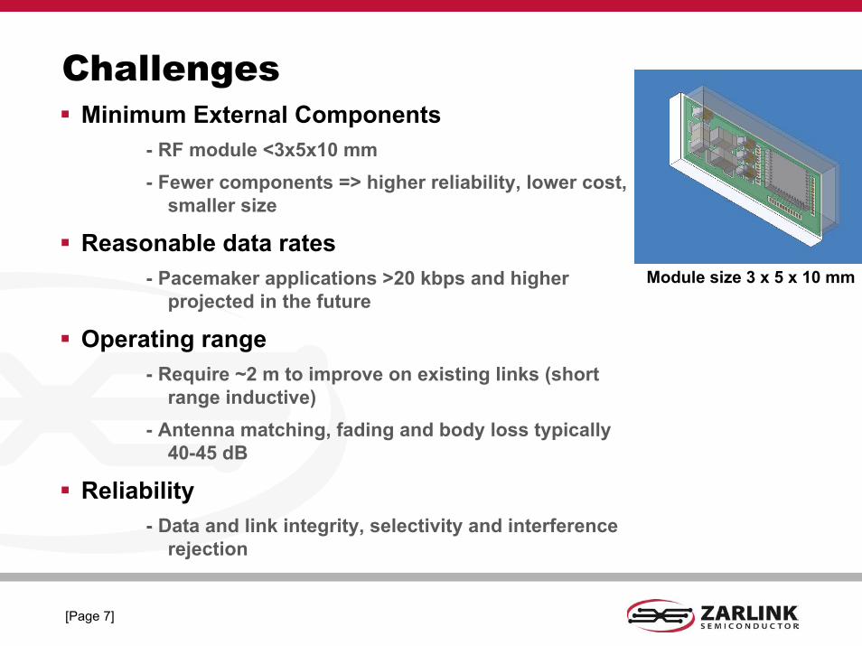
Module size 3 x 5 x 10 mm

[Page 8]
Design Solutions Key Concept - Duty Cycle
- Duty cycle normal data exchange for given data rate- Duty cycle sniffing for wakeup- Turn off sub-systems in chip when not required.
Use the highest possible data rate for required sensitivity- Apply concept even for systems that require low data rates
(low kHz range)- Sending data in short bursts conserves power- Reduces time window for interference and easier supply decoupling
High Data Integrity- Reed-Solomon Forward Error Correction, CRC error detection- Capable of several years continuous operation without error
High Level of Integration- Sub-micron CMOS RF technology- Integrated filters

[Page 9]
ULP Implantable Transceiver (ZL70101)
Technology: 0.18 um RF CMOSSupply Voltage: 2.1 - 3.5 V BatteryRadio Frequency: 402-405 MHz / 433 MHzType of RF link Bi-directional, half duplexModulation Scheme: FSKRaw Bit Rate: 800 / 400 / 200 kbits/sOperating Current: 5mA TX/RX down to <1mASleep Current: < 250 nAExt. comps: 3 (2 caps, Xtal) + antenna matching)BER: < 1.5 x 10⁻¹⁰
Range: ~2 mInterface: SPI
QFN package shown, also available as wire
bondable bare die
MICS and ISM Band Transceiver:• Negligible standby current• high data and low error rates in a small footprint

[Page 10]
ZL70101 MICS System
Multiple Startup Methods
– 2.45 GHz signal– Pin Control
(for Emergency messages, 400 MHz sniffing, low frequency inductive link sniffing or other wakeup methods)
Extremely Low Power– 5 mA continuous TX/RX– <1mA low power mode
Ultra Low Power Wake-up Circuit– <250 nA
0.9 mA TX/RX mode
5.0 mA
Power-save time (0-27 s)

[Page 11]
ZL70101 Block Diagram
Zarlink MICS Transceiver - ZL70101
Media Access Controller
VDD
IO
VSSD
tx_clk
tx_data
rx_data
PDCTRLXO_BYPASS
Input Pin Pull -down Control Bypass of on -chip Crystal Oscillator Control
Decoupling Capacitors
RX
TX + TX IF Modulator
RF 400 MHz
RF 400 MHz
400 MHz Transceiver
RF_RX
RF_TX
XTAL
2
XTAL
1
Mixer
MixerPower Amplifier
Linear Amplifier
5bit ADC
ADC analog Inputs(TESTIO [4:1] pins)
RX IF Filter and FM Detector
RX ADC
PLL
DataBus
Peak Detectors
MATCH1MATCH2
Matching nework
Battery or Other Supply
68nF 68nF
RXRF 2.45 GHz
2.45 GHz Wake-Up Receiver
VSU
P
RX_245
ULP Osc
VDD
DWake-Up Control
Regulator1.9 - 2.0V
Regulator1.9 - 2.0V
VDD
A
VSSA
Anal
og T
est
TEST
IO[6
:5]
To ADC Mux
2
4
RSSI
Analog Inputs 4
WU_EN
Select IMD or Base Transceiver
Wakeup IMDIBS
VREG_MODESelect one or two regulators
Correlator
Clock Recovery
RX Control
Message Storage
CRC Decode
RS Decode
Control
TX Control
InterfaceSPI
MODE[1:0]Test Mode Control
IRQ
2
Message Storage
CRC Generation
RS EncoderWhitening
PO[4:0]PI[2:0]
53
ProgrammableIO
SPI_SDOSPI_SDISPI_CLKSPI_CS_B
SPI Interface
24 MHz

[Page 12]
Wakeup ReceiverProblem: MICS band limited to 25 uW (-16 dBm)Solution: Use band with more power 2.45 GHz (up to 20 dBm) and design synthesizer-less receiver – High Gain LNA and OOK detector– Manchester coding of pulses– 250 nA average current for 1.15 second latency
Possible to use for other sniffing/wakeup applications
WU_EN

[Page 13]
The Camera Pill(Company: Given Imaging)
New digestive track diagnostic toolReplace endoscopyBetter diagnostic
Healthy Small Bowel

[Page 14]
The Camera Pill - Facts
Size: 11 x 26 mm
Weight: < 4 gram
View: 140 deg
Approximately 57,000 pictures
During 8 hours

[Page 15]
The Camera Pill – The InsideWorld’s First Swallowable Camera Capsule, from Given Imaging, including Zarlink’s ULP RF Transmitter
Zarlink’s RF chip

[Page 16]
ULP Medical Transmitter (ZL70081)
Technology: 0.35µm CMOS Supply Voltage 2.6 - 3.2 V BatteryRadio Frequency: 400 - 440 MHzType of RF link: Transmit onlyBit Rate: 2700 kbits/sOperating Power: 5.2 mWExt. comps: 10
Very high data rate transmitterlow powersmall footprint designed for imaging applications

[Page 17]
Hearing Aids are becoming Communication Devices
Programming would be easier, more reliable and cheaper without cable.Ear-to-ear communication can improve hearing by coming closer to a real stereo image.Streaming audio allow connection to cell phone and MP3 player.
But power consumption is limited– HA need to last 1 – 2 weeks, 16h/day– Battery size is limited (typ ~250 mA.h)– HA functionality is ~1mA– RF budget should be < 20%

[Page 18]
ULP Transceiver (ZL70250)Hearing Aid wireless link:
• Device programming• Ear to ear communication for active noise cancellation, directional hearing and volume control• Audio streaming
Technology: 0.18 µm RF CMOSRadio Frequency: 915 MHz (Americas) / 863-865 MHz (Europe)Type of RF link: Bi-directional, half duplexBit Rate: 186 kbits/sCurrent Consumption: <2 mA from 1.05 - 1.5 V Battery Range: 3 meters (limited by antenna size)Externals: 2 (Xtal,Res)Interface: SPI + 2-wire
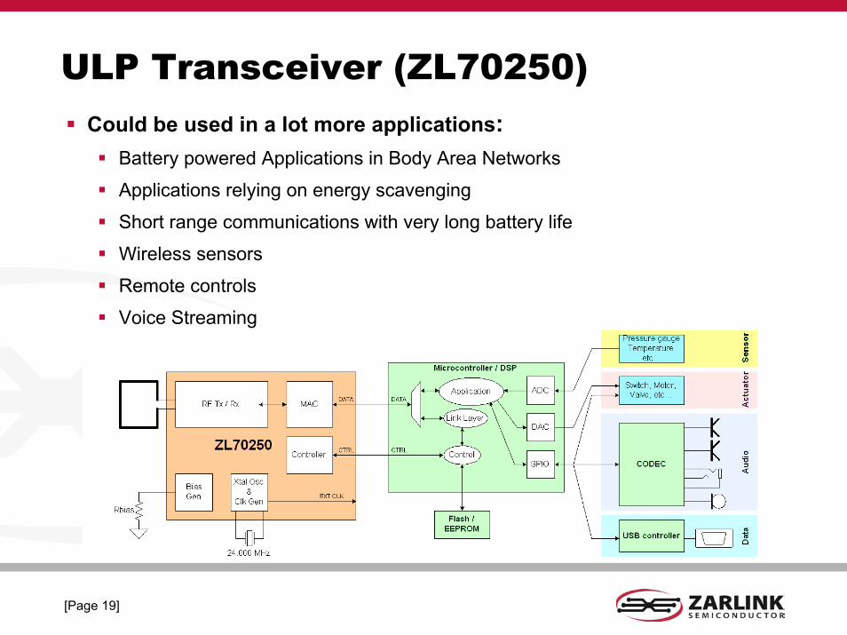
[Page 19]
ULP Transceiver (ZL70250)Could be used in a lot more applications:
Battery powered Applications in Body Area Networks
Applications relying on energy scavenging
Short range communications with very long battery life
Wireless sensors
Remote controls
Voice Streaming

[Page 20]
Conclusion RF integrated circuits for the MICS and ISM bands will open up a new range of clinical applications for the next generation medical devices.
The development of such circuits requires cutting edge technology and design with specific attention to power consumption.
Integrated circuits, modules are available now and are being used in the latest medical devices development.
Other applications could benefits from this Ultra Low Power RF technology

Zarlink Semiconductor