rf model of flexible microwave single-crystalline silicon ... by...rf model of flexible microwave...
TRANSCRIPT

Microelectronics Journal 42 (2011) 509–514
Contents lists available at ScienceDirect
Microelectronics Journal
0026-26
doi:10.1
n Corr
Engineenn Als
Electric
Tel./fax:
E-m
mazq@e
journal homepage: www.elsevier.com/locate/mejo
RF model of flexible microwave single-crystalline silicon nanomembranePIN diodes on plastic substrate
Guoxuan Qin a,b,n, Hao-Chih Yuan b, George K. Celler c, Weidong Zhou d, Jianguo Ma a, Zhenqiang Ma b,nn
a Tianjin University, School of Electronic Information Engineering, Tianjin 300072, PR Chinab University of Wisconsin-Madison, Department of Electrical and Computer Engineering, Madison, WI 53706, USAc Soitec USA, 2 Centennial Drive, Peabody, MA 01960, USAd University of Texas at Arlington, Department of Electrical Engineering, Arlington, TX 76019, USA
a r t i c l e i n f o
Article history:
Received 1 September 2010
Accepted 18 October 2010Available online 11 November 2010
Keywords:
Flexible PIN diode
Microwave
Modeling
Nanomembrane
Plastic substrate
Radio frequency (RF)
Single-crystalline silicon
92/$ - see front matter & 2010 Elsevier Ltd. A
016/j.mejo.2010.10.012
esponding author at: Tianjin University, Scho
ring, Tianjin 300072, PR China. Tel.: 86 22 27
o Corresponding author. University of Wiscon
al and Computer Engineering, Madison, WI 53
1 608 261 1095.
ail addresses: [email protected], guoxuanqin@h
ngr.wisc.edu (Z. Ma).
a b s t r a c t
This paper reports the realization and RF modeling of flexible microwave P-type-Intrinsic-N-type (PIN)
diodes using transferrable single-crystalline Si nanomembranes (SiNMs) that are monolithically
integrated on low-cost, flexible plastic substrates. With high-energy, high-dose ion implantation and
high-temperature annealing before nanomembrane release and transfer process, the parasitic para-
meters (i.e. resistance, inductance, etc.) are effectively reduced, and the flexible PIN diodes achieve good
high-frequency response. With consideration of the flexible device fabrication, structure and layout
configuration, a RF model of the microwave single-crystalline Si nanomembrane PIN diodes on plastic
substrate is presented. The RF/microwave equivalent circuit model achieves good agreement with the
experimental results of the single-crystalline SiNM PIN diodes with different diode areas, and reveals the
most influential factors to flexible diode characteristics. The study provides guidelines for properly
designing and using single-crystalline SiNMs for flexible RF/microwave diodes and demonstrates the
great possibility of flexible monolithic microwave integrated systems.
& 2010 Elsevier Ltd. All rights reserved.
1. Introduction
There has been increasing enthusiasm on high performance,large-area flexible electronics for the past few years, because oftheir unique advantages such as bendability, light weight, andconformally attachable to any shape of surfaces [1]. Variousapplications are now employing the flexible micro- and macro-electronics, including large-area displays, electronic textile/paper,biomedical sensors, etc. [2–6]. Amorphous silicon, organics andpolymers, and polycrystalline silicon are the most commonly usedmaterials for the low-speed flexible electronics [1,4,6]. However,due to their poor crystalline quality and carrier mobility, thesematerials are not suitable for applications that require high-speedand high frequency operations, e.g. RFIDs, portable Wi–Fi devices,flexible airborne/space-borne communication systems, and sur-veillance and remote sensing radars [1,7]. Recently developedtransferrable and flexible single-crystalline Si nanomembrane
ll rights reserved.
ol of Electronic Information
408761.
sin-Madison, Department of
706, USA.
otmail.com (G. Qin),
(SiNM), lifted from silicon-on-insulator: SOI wafers, makes fastelectronics possible. The high carrier mobility of SiNMs, which is ashigh as their rigid bulk wafer counterparts [8–11], makes thempromising for very high-frequency applications.
To transform the superior carrier transport characteristics ofSiNMs into high-speed thin-film transistors (TFTs), we havedeveloped a unique combined high-temperature and low-temperature process for transferrable SiNMs [11]. This led to therealization of microwave TFTs on a plastic substrate [11,12]. Otherthan active transistors, in order to build the flexible monolithicmicrowave integrated circuits, passive components that can beoperated at RF/microwave frequency are indispensable. Further-more, to accurately and efficiently design the flexible microwaveintegrated circuits, RF/microwave model of the PIN diodes isessential. However, all the available models for PIN diodes arebased on bulky rigid wafers, accurate modeling of the novelmicrowave PIN diodes using single-crystalline SiNMs on plasticsubstrate is not yet reported.
There are two kinds of models commonly used: physical modeland equivalent circuit model. Although a physical model canprecisely predict single device 2D or 3D characteristics, it requiresabundant numerical complexity [13], thus it is not suitable forcircuit designs. On the other hand, an equivalent circuit model canprovide sufficiently accurate performance at the device or circuitlevel, with much fewer model parameters and less computation

G. Qin et al. / Microelectronics Journal 42 (2011) 509–514510
time. In this paper, we develop an RF/microwave equivalent circuitmodel for the microwave PIN diodes using transferable SiNMs onplastic substrate. The model provides guidelines for designing andusing PIN diodes in flexible MMICs based on single-crystalline Sinanomembranes on plastic substrates.
2. Device fabrication
For the goal of flexible monolithic microwave integratedcircuits, the fabrication process of the PIN diodes using transferableSiNMs on plastic substrate is fully compatible with that used tofabricate active transistors (TFTs) [11]. This process allows simul-taneous fabrication of the active TFTs and passive PIN diodes on thesame plastic substrate.
The process flow is briefly illustrated as shown in Fig. 1. Thefabrication process begins with a lightly-doped p-type Si (0 0 1) SOIsubstrate with a 200-nm Si top layer and 200-nm buried oxide(BOX) layer. Align marks and the lateral n- and p-type regions wereformed by optical photolithography. The patterned SOI samplethen received ion implantation of phosphorus ions and boron ions,respectively, to form heavily doped n- and p-type regions. Thesample was annealed at 850 1C for 45 min in N2 ambient in afurnace (Fig. 1(a)). The well-controlled high-energy, heavily dosedion implantation, and high temperature furnace annealing enablelow contact and sheet resistance and thus low parasitic effects,which are the critical process steps to fabricate RF/microwaveactive and passive devices.
The 200-nm Si template layer was then patterned into strips ormembrane with array of holes, followed by a plasma dry etching(SF6/O2) down to the BOX layer (Fig. 1(b)). After stripping off the
Fig. 1. Process schematic of fabricating flexible microwave single-crystalline Si nanomem
dosed n- and p-type regions by lithography patterning, ion implantation and high-temp
down to the buried oxide (BOX) layer by dry etching. (c) 200 nm single-crystalline Si nan
BOX layer in HF solution. (d) The Si nano-stripes (or SiNMs) are brought firmly contacted
handling substrate. (e) The Si nano-stripes (or SiNMs) are flip-transferred onto the pla
crystalline SiNMs on plastic substrate, after dry etching the SiNM active area and evap
crystalline SiNM PIN diodes under bending condition.
photoresist, the sample was put into diluted hydrofluoric acid (HF)to etch away the underlying BOX layer and release the SiNMsweakly bonded on the Si handling substrate wafer via van derWaals forces (Fig. 1(c)) [14].
Then the sample was rinsed thoroughly with DI water and wassubsequently brought face-to-face and firmly contacted with a�175 mm thick polyethylene terephthalate (PET) substrate thatwas spin-coated with a SU-8 epoxy layer. Since the bonding forcebetween the SiNM and the epoxy is stronger than the Si-to-Sibonding, the SiNM can be lifted off from the SOI substrate (Fig. 1(d))and flip-transferred onto the PET substrate (Fig. 1(e)). This fliptransfer technique makes the displacement of patterned Si-stripsas small as possible after they were transferred onto the plasticsubstrate [12,15]. A UV exposure step was then used to curethe SU-8.
SiNMs were then selectively dry etched into smaller active arearegions to further enhance the device flexibility. Finally, metalcontacts and interconnects were formed by evaporating and a lift-off process (Fig. 1(f)). The highest temperature applied to the plasticsubstrates was kept below 120 1C.
The lateral arrangement of the PIN structure in this study hastwo major advantages: firstly, it allows simultaneous photolitho-graphy patterning and n-/p-type ion implantation for active TFTsand passive PIN diodes. Secondly, the lateral structure is notcompromising the thinness of the SiNMs and thus device flexibility.The width of the I-region is determined by the distance betweenthe p+ and n+ regions during photolithography. An I-region widthof 2 mm is used in this study in order to achieve high-frequencyresponse while maintaining proper breakdown voltages for powerhandling. The diode cross-section area can be calculated by multi-plying the width of the p+ (or n+) region by the thickness of the
brane PIN diode on plastic substrate (drawn not to scale). (a) SOI sample with heavily
erature annealing. (b) 200 nm template Si layer is patterned into stripes and etched
ostripes are released and attached on handling substrate wafer, by etching away the
with PET plastic substrate with adhersive spinned SU-8 layer, and detached from the
stic substrate. (f) Finished flexible microwave PIN diode using transferable single-
orating the metal connection and electrodes. (g) Illustration of the flexible single-

Fig. 2. (a) Optical image of the finished PIN diodes arrays on a bent PET substrate. (b) Microscopic image of the flexible microwave single-crystalline SiNM PIN diode on plastic
substrate. Total diode width is 400 mm (two identical parallel diode channel, each channel has a width of 200 mm). Diode intrinsic region length is 2 mm. Total diode area is
80 mm2. (c) Microscopic image of the 240 mm2-PIN diode on plastic substrate. Total diode width is 1200 mm (two identical parallel diode channels, each channel has a width of
600 mm).
Fig. 3. (a) Equivalent circuit schematic of a p–n junction. (b) RF/microwave
equivalent circuit model for microwave PIN diodes using transferable single-
crystalline SiNMs on plastic substrate.
G. Qin et al. / Microelectronics Journal 42 (2011) 509–514 511
SiNM (200 nm). The fabricated diodes have various areas rangingfrom 80 mm2 (total diode width is 400 mm) to 240 mm2 (total diodewidth is 1200 mm). Fig. 2(a) shows an optical image of the flexiblePIN diodes and switch arrays on PET substrate. Fig. 2(b) and (c)shows the optical-microscope images of finished lateral SiNM PINdiodes with an area of 80 and 240 mm2, respectively.
3. RF model and experimental results
The RF/microwave equivalent circuit model of the microwavelateral PIN diode using single-crystalline SiNMs on plastic substrateis composed of three major parts according to the device structureand layout as depicted in Fig. 3.
1.
JunctionsThe lateral PIN diode consists of two junctions: A p–n+ junctionand a p+p- junction. Under forward mode condition, theequivalent circuit model for the p–n+ junction is shown inFig. 3(a) [16]. The resistor value is small and can be expressed asshown in Eq. (1). The parallel capacitor is composed of space-charge region capacitance and diffusion capacitance, asexpressed in Eqs. (2)–(9) [16]. When the PIN diode is zero orreversely biased, the resistor value is large and omitted as anopen circuit for the simplicity without loosing the generality.The parallel capacitor is mainly space-charge region capaci-tance, as shown in Eq. (3), where reverse bias VAr is applied.
R¼kT
qAJð1Þ
C ¼ CTþCD ð2Þ
CT ¼ A
ffiffiffiffiffiffiffiffiffiffiffiffiffiffiffiffiffiffiffiffiffiffieqNA
2ðVBJ�VAÞ
sð3Þ
CD ¼ Aq2
kTLnnp0exp
qVA
kT
� �ð4Þ
VBJ ¼kT
qln
NAND
n2i
!ð5Þ
VA ¼kT
qln
J
J0
� �ð6Þ
J0 ¼qDnnp0
Lnþ
qDppn0
Lpð7Þ
np0 ¼n2
i
NA, pn0 ¼
n2i
NDð8Þ
Lp ¼
ffiffiffiffiffiffiffiffiffiffiffiffiffiffiffiffimpkTtp
q, Ln ¼
ffiffiffiffiffiffiffiffiffiffiffiffiffiffiffiffimnkTtn
qð9Þ
The p+p- junction has the similar equivalent circuit topology asused for the p–n+ junction model, with only change to the built-in voltage expression and saturation current density, as shownin Eqs. (10) and (11).
VBJ2 ¼kT
qln
pp01
pp02
� �ð10Þ
J02 ¼qDppn0
Lpð11Þ
2.
Intrinsic regionThe intrinsic region of the PIN diode can be modeled as avariable resistor, under forward and reverse bias conditions. TheI-region resistance under forward-biased condition can be
G. Qin et al. / Microelectronics Journal 42 (2011) 509–514512
expressed as
Ri ¼w2
i
If tðmnþmpÞð12Þ
where wi is the width of the I-region, If is the forward-biased current,and t is the effective carrier lifetime. mn, mp are the mobilities ofelectrons and holes, respectively. The I-region resistance will bemuch larger at zero or reverse bias, because of the carrier fullydepletion region.
3.
Fig. 4. Measured small-signal S-parameters (solid red curves) of the flexible
microwave PIN diode (diode area¼240 mm) under ON state (forward mode),
with comparison of the calculated results using developed RF model (dashed
blue curves). (a) S21, insertion loss. (b) S11, return loss. (For interpretation of the
references to color in this figure legend, the reader is referred to the web version of
this article.)
ParasiticsFor the microwave single-crystalline SiNM PIN diodes on plasticsubstrates, since novel nanoscale single-crystalline Si membraneis employed for fabricating PIN diodes and soft PET substrate isused, parasitic effects are more severe than those on rigid bulk Sisubstrates. Therefore parasitic parameters need to be carefullyinvestigated and included in the RF equivalent circuit model.Series parasitic resistor and inductor are mainly induced byconnection metals, electrode contact resistance, and thin SiNMs.According to the flexible device layout, parasitic capacitancebetween input and output is nonnegligible. As shown in themicroscopic image (Fig. 2(b)), the parasitic capacitor is composedof two parallel plate capacitors between the input and outputconnection metal, and can be approximately expressed as Eq. (13).Where t is the connection metal thickness, w is the input andoutput metal overlap width (roughly diode width), and d is thespacing between input and output metal (roughly diode intrinsicregion length). Therefore the parasitic capacitance is roughlyproportional to the diode area, and reversely proportional to thediode intrinsic region length. The parasitic parameters are almostindependent of the diode bias condition.
Cpara �2ee0tw
dð13Þ
With the three parts, the RF/microwave equivalent circuit modelfor flexible PIN diode on plastic substrate is shown in Fig. 3(b).Where intrinsic region resistor and series parasitic resistor arecombined for simplicity. The model is put into Agilent AdvancedDesign System (ADS) to calculate the RF/microwave response ofthe flexible PIN diodes.
RF characteristics of the PIN diodes were measured with anAgilent E8364A performance network analyzer using 150-mm pitchCascade Ground-Signal-Ground (GSG) probes. Calibration wasconducted to the probe tip by Short-Open-Load-Thru (SOLT)method using impedance standard substrate from DC to 40 GHz.Small-signal scattering parameters (S-parameters) were measuredfor the SiNM PIN diodes under both ON (diode is forward biased,forward current If¼10 mA) and OFF (diode is zero biased) condi-tions. (DC and power handling capability of the flexible PIN diodeswere also measured) [15,17]. Under this state, RF signal istransmitted from the IN port to the OUT port. The power ratio ofthe signal between the OUT port and the IN port through the diodeunder ON state is defined as insertion loss (S21, in dB). Themeasured RF signal power ratio between the OUT port and theIN port under OFF state is defined as isolation (also S21, in dB).
The experimental data for a 240-mm2 SiNM PIN diode from DC to20 GHz are shown in Fig. 4 (forward mode ON state) and Fig. 5(reverse mode OFF state). The insertion loss of the 240-mm2 SiNMPIN diode is less than 1.5 dB up to 20 GHz. Isolation of 411 dB isobserved up to 5 GHz and degrades at higher frequencies. Theflexible PIN diode using transferable single-crystalline SiNMs onplastic substrate demonstrates good frequency response at RF andmicrowave frequency regime, indicating great potential of mono-lithic integration of flexible active and passive devices on flexiblesubstrates for RF/microwave applications. The fluctuations of the
measured data are possibly due to the worse contact between theGSG probe and thin metal electrode on soft substrate.
The modeled results for ON and OFF states using the RF/microwave model are also shown in Figs. 4 and 5 for comparisons.Measurement and calculation results are further obtained andcompared for an 80-mm2 SiNM PIN diode for validating thedeveloped model, as shown in Fig. 6 (ON state) and Fig. 7 (OFFstate). Good agreements are achieved for both diodes underforward and reverse bias conditions. The discrepancy betweenexperimental data and calculation is mainly because of the notperfect contact of the probes on soft substrates. Overall, Figs. 4–7demonstrate good accuracy of the RF/microwave model for themicrowave PIN diodes using single-crystalline SiNMs on plasticsubstrates.
4. Discussion
According to Figs. 4–7, it can be seen that flexible PIN diode withsmaller diode area has worse insertion loss (more degradation)

Fig. 5. Measured small-signal S-parameters (solid red curves) of the flexible
microwave PIN diode (diode area¼240 mm) under OFF state, with comparison of
the calculated results using developed RF model (dashed blue curves). (a) S21,
isolation. (b) S11, forward mode return loss. (For interpretation of the references to
color in this figure legend, the reader is referred to the web version of this article.)
Fig. 6. Measured small-signal S-parameters (solid red curves) of the flexible
microwave PIN diode (diode area¼80 mm) under ON state (forward mode), with
comparison of the calculated results using developed RF model (dashed blue
curves). (a) S21, insertion loss. (b) S11, forward mode return loss. (For interpretation
of the references to color in this figure legend, the reader is referred to the web
version of this article.)
G. Qin et al. / Microelectronics Journal 42 (2011) 509–514 513
at forward bias, but better isolation characteristic at reverse bias.With the RF/microwave model, underlying reason is analyzed.Under forward bias mode, the series resistance is 14.2 O and theparasitic inductance is 0.133 nH for the 240 mm PIN diode. Whenthe diode area is decreasing to 80 mm, the series resistanceincreases to 19 O. The increasing is not proportional to the diodearea change because that series resistance consists of intrinsicregion resistance and parasitic resistance. When the diode areabecomes smaller, intrinsic region resistance increases because ofsmaller diode width, while the parasitic resistance is reduced dueto shorter connection metal length. The high series resistance iscontributed from the thinness of the SiNMs and relatively largeintrinsic region length for power handling capability. Smaller diodeintrinsic region length is able to significantly reduce the seriesresistance. Different from the series resistance, the parasiticinductance is decreased from 0.133 to 0.126 nH for the PIN diodewith 80 mm diode area, because of shorter connection metal lengthfrom input port to output port. Under reverse bias mode, seriesresistance of 240 mm PIN diode is 40.2 Owhile it increases to 120 Ofor the 80 mm PIN diode, approximately follows the reverselyproportional increasement with diode area. This is because that
under reverse bias condition, the intrinsic region resistancedominates the series resistance, therefore the diode shows seriesresistance reversely proportional to the diode area. Parasiticinductance shows similar change with that under forward mode,since parasitic inductance is much less sensitive to the diode widththan resistance. In addition, all the capacitance (including junctioncapacitance and parasitic capacitance) shows proportional changewith the PIN diode area. With good understanding of the deviceparameters based on RF/microwave model, higher series resistanceis demonstrated to be the major factor for lower insertion loss andbetter isolation. The model shows a performance trade-off betweenforward mode insertion loss and reverse mode isolation withdifferent flexible PIN diode structures. Furthermore, the modelprovides a guideline of designing and optimizing the flexible PINdiodes for RF/microwave applications.
5. Conclusion
Flexible microwave PIN diodes using transferrable single-crystal Sinanomembranes (SiNM) that are monolithically integrated on low-cost
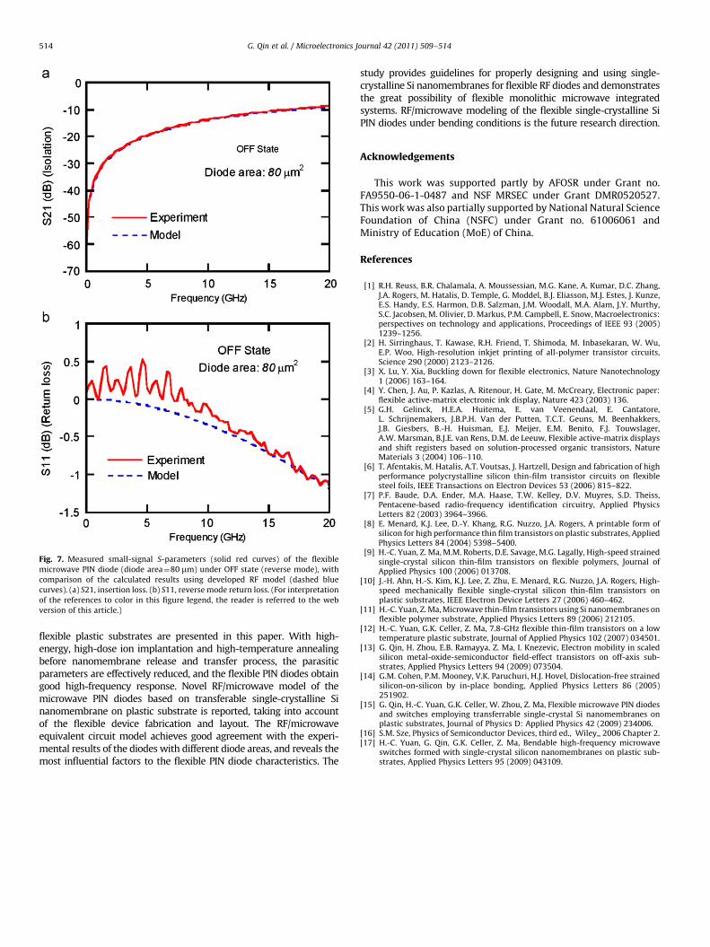
Fig. 7. Measured small-signal S-parameters (solid red curves) of the flexible
microwave PIN diode (diode area¼80 mm) under OFF state (reverse mode), with
comparison of the calculated results using developed RF model (dashed blue
curves). (a) S21, insertion loss. (b) S11, reverse mode return loss. (For interpretation
of the references to color in this figure legend, the reader is referred to the web
version of this article.)
G. Qin et al. / Microelectronics Journal 42 (2011) 509–514514
flexible plastic substrates are presented in this paper. With high-energy, high-dose ion implantation and high-temperature annealingbefore nanomembrane release and transfer process, the parasiticparameters are effectively reduced, and the flexible PIN diodes obtaingood high-frequency response. Novel RF/microwave model of themicrowave PIN diodes based on transferable single-crystalline Sinanomembrane on plastic substrate is reported, taking into accountof the flexible device fabrication and layout. The RF/microwaveequivalent circuit model achieves good agreement with the experi-mental results of the diodes with different diode areas, and reveals themost influential factors to the flexible PIN diode characteristics. The
study provides guidelines for properly designing and using single-crystalline Si nanomembranes for flexible RF diodes and demonstratesthe great possibility of flexible monolithic microwave integratedsystems. RF/microwave modeling of the flexible single-crystalline SiPIN diodes under bending conditions is the future research direction.
Acknowledgements
This work was supported partly by AFOSR under Grant no.FA9550-06-1-0487 and NSF MRSEC under Grant DMR0520527.This work was also partially supported by National Natural ScienceFoundation of China (NSFC) under Grant no. 61006061 andMinistry of Education (MoE) of China.
References
[1] R.H. Reuss, B.R. Chalamala, A. Moussessian, M.G. Kane, A. Kumar, D.C. Zhang,J.A. Rogers, M. Hatalis, D. Temple, G. Moddel, B.J. Eliasson, M.J. Estes, J. Kunze,E.S. Handy, E.S. Harmon, D.B. Salzman, J.M. Woodall, M.A. Alam, J.Y. Murthy,S.C. Jacobsen, M. Olivier, D. Markus, P.M. Campbell, E. Snow, Macroelectronics:perspectives on technology and applications, Proceedings of IEEE 93 (2005)1239–1256.
[2] H. Sirringhaus, T. Kawase, R.H. Friend, T. Shimoda, M. Inbasekaran, W. Wu,E.P. Woo, High-resolution inkjet printing of all-polymer transistor circuits,Science 290 (2000) 2123–2126.
[3] X. Lu, Y. Xia, Buckling down for flexible electronics, Nature Nanotechnology1 (2006) 163–164.
[4] Y. Chen, J. Au, P. Kazlas, A. Ritenour, H. Gate, M. McCreary, Electronic paper:flexible active-matrix electronic ink display, Nature 423 (2003) 136.
[5] G.H. Gelinck, H.E.A. Huitema, E. van Veenendaal, E. Cantatore,L. Schrijnemakers, J.B.P.H. Van der Putten, T.C.T. Geuns, M. Beenhakkers,J.B. Giesbers, B.-H. Huisman, E.J. Meijer, E.M. Benito, F.J. Touwslager,A.W. Marsman, B.J.E. van Rens, D.M. de Leeuw, Flexible active-matrix displaysand shift registers based on solution-processed organic transistors, NatureMaterials 3 (2004) 106–110.
[6] T. Afentakis, M. Hatalis, A.T. Voutsas, J. Hartzell, Design and fabrication of highperformance polycrystalline silicon thin-film transistor circuits on flexiblesteel foils, IEEE Transactions on Electron Devices 53 (2006) 815–822.
[7] P.F. Baude, D.A. Ender, M.A. Haase, T.W. Kelley, D.V. Muyres, S.D. Theiss,Pentacene-based radio-frequency identification circuitry, Applied PhysicsLetters 82 (2003) 3964–3966.
[8] E. Menard, K.J. Lee, D.-Y. Khang, R.G. Nuzzo, J.A. Rogers, A printable form ofsilicon for high performance thin film transistors on plastic substrates, AppliedPhysics Letters 84 (2004) 5398–5400.
[9] H.-C. Yuan, Z. Ma, M.M. Roberts, D.E. Savage, M.G. Lagally, High-speed strainedsingle-crystal silicon thin-film transistors on flexible polymers, Journal ofApplied Physics 100 (2006) 013708.
[10] J.-H. Ahn, H.-S. Kim, K.J. Lee, Z. Zhu, E. Menard, R.G. Nuzzo, J.A. Rogers, High-speed mechanically flexible single-crystal silicon thin-film transistors onplastic substrates, IEEE Electron Device Letters 27 (2006) 460–462.
[11] H.-C. Yuan, Z. Ma, Microwave thin-film transistors using Si nanomembranes onflexible polymer substrate, Applied Physics Letters 89 (2006) 212105.
[12] H.-C. Yuan, G.K. Celler, Z. Ma, 7.8-GHz flexible thin-film transistors on a lowtemperature plastic substrate, Journal of Applied Physics 102 (2007) 034501.
[13] G. Qin, H. Zhou, E.B. Ramayya, Z. Ma, I. Knezevic, Electron mobility in scaledsilicon metal-oxide-semiconductor field-effect transistors on off-axis sub-strates, Applied Physics Letters 94 (2009) 073504.
[14] G.M. Cohen, P.M. Mooney, V.K. Paruchuri, H.J. Hovel, Dislocation-free strainedsilicon-on-silicon by in-place bonding, Applied Physics Letters 86 (2005)251902.
[15] G. Qin, H.-C. Yuan, G.K. Celler, W. Zhou, Z. Ma, Flexible microwave PIN diodesand switches employing transferrable single-crystal Si nanomembranes onplastic substrates, Journal of Physics D: Applied Physics 42 (2009) 234006.
[16] S.M. Sze, Physics of Semiconductor Devices, third ed., Wiley,, 2006 Chapter 2.[17] H.-C. Yuan, G. Qin, G.K. Celler, Z. Ma, Bendable high-frequency microwave
switches formed with single-crystal silicon nanomembranes on plastic sub-strates, Applied Physics Letters 95 (2009) 043109.