rfd21731 13715 alton pkwy - mouser electronics rf digital brochure-1111.pdf · 13715 alton pkwy •...
TRANSCRIPT
13715 Alton Pkwy • Irvine • CA • 92618 Tel: 949.610.0008 • Fax: 949.610.0009
www.rfdigital.com • [email protected]
1
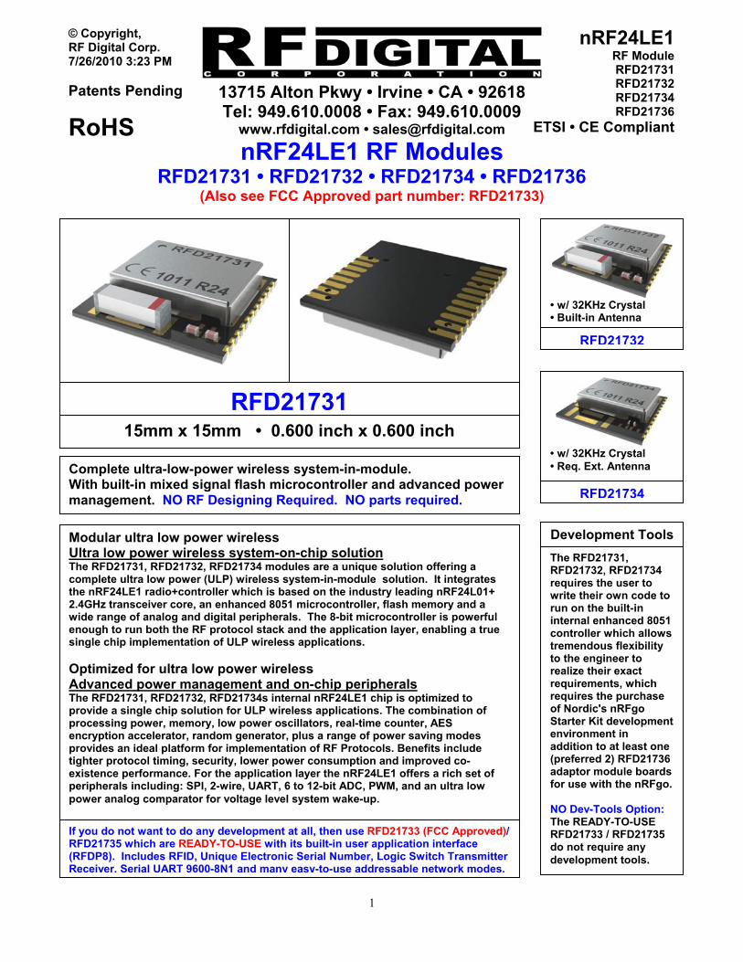
nRF24LE1RF ModuleRFD21731RFD21732RFD21734RFD21736
ETSI • CE Compliant
© Copyright, RF Digital Corp. 7/26/2010 3:23 PM Patents Pending
RoHS nRF24LE1 RF Modules
RFD21731 • RFD21732 • RFD21734 • RFD21736 (Also see FCC Approved part number: RFD21733)
RFD21732
• w/ 32KHz Crystal • Built-in Antenna
• w/ 32KHz Crystal • Req. Ext. Antenna
RFD21734
RFD21731
Modular ultra low power wireless Ultra low power wireless system-on-chip solution The RFD21731, RFD21732, RFD21734 modules are a unique solution offering a complete ultra low power (ULP) wireless system-in-module solution. It integrates the nRF24LE1 radio+controller which is based on the industry leading nRF24L01+ 2.4GHz transceiver core, an enhanced 8051 microcontroller, flash memory and a wide range of analog and digital peripherals. The 8-bit microcontroller is powerful enough to run both the RF protocol stack and the application layer, enabling a true single chip implementation of ULP wireless applications. Optimized for ultra low power wireless Advanced power management and on-chip peripherals The RFD21731, RFD21732, RFD21734s internal nRF24LE1 chip is optimized to provide a single chip solution for ULP wireless applications. The combination of processing power, memory, low power oscillators, real-time counter, AES encryption accelerator, random generator, plus a range of power saving modes provides an ideal platform for implementation of RF Protocols. Benefits include tighter protocol timing, security, lower power consumption and improved co-existence performance. For the application layer the nRF24LE1 offers a rich set of peripherals including: SPI, 2-wire, UART, 6 to 12-bit ADC, PWM, and an ultra low power analog comparator for voltage level system wake-up.
15mm x 15mm • 0.600 inch x 0.600 inch
Complete ultra-low-power wireless system-in-module. With built-in mixed signal flash microcontroller and advanced power management. NO RF Designing Required. NO parts required.
The RFD21731, RFD21732, RFD21734 requires the user to write their own code to run on the built-in internal enhanced 8051 controller which allows tremendous flexibility to the engineer to realize their exact requirements, which requires the purchase of Nordic's nRFgo Starter Kit development environment in addition to at least one (preferred 2) RFD21736 adaptor module boards for use with the nRFgo. NO Dev-Tools Option: The READY-TO-USE RFD21733 / RFD21735 do not require any development tools.
Development Tools
If you do not want to do any development at all, then use RFD21733 (FCC Approved)/ RFD21735 which are READY-TO-USE with its built-in user application interface (RFDP8). Includes RFID, Unique Electronic Serial Number, Logic Switch Transmitter Receiver, Serial UART 9600-8N1 and many easy-to-use addressable network modes.
13715 Alton Pkwy • Irvine • CA • 92618 Tel: 949.610.0008 • Fax: 949.610.0009
www.rfdigital.com • [email protected]
2
nRF24LE1RF ModuleRFD21731RFD21732RFD21734RFD21736
ETSI • CE Compliant
© Copyright, RF Digital Corp. 7/26/2010 3:23 PM Patents Pending
RoHS
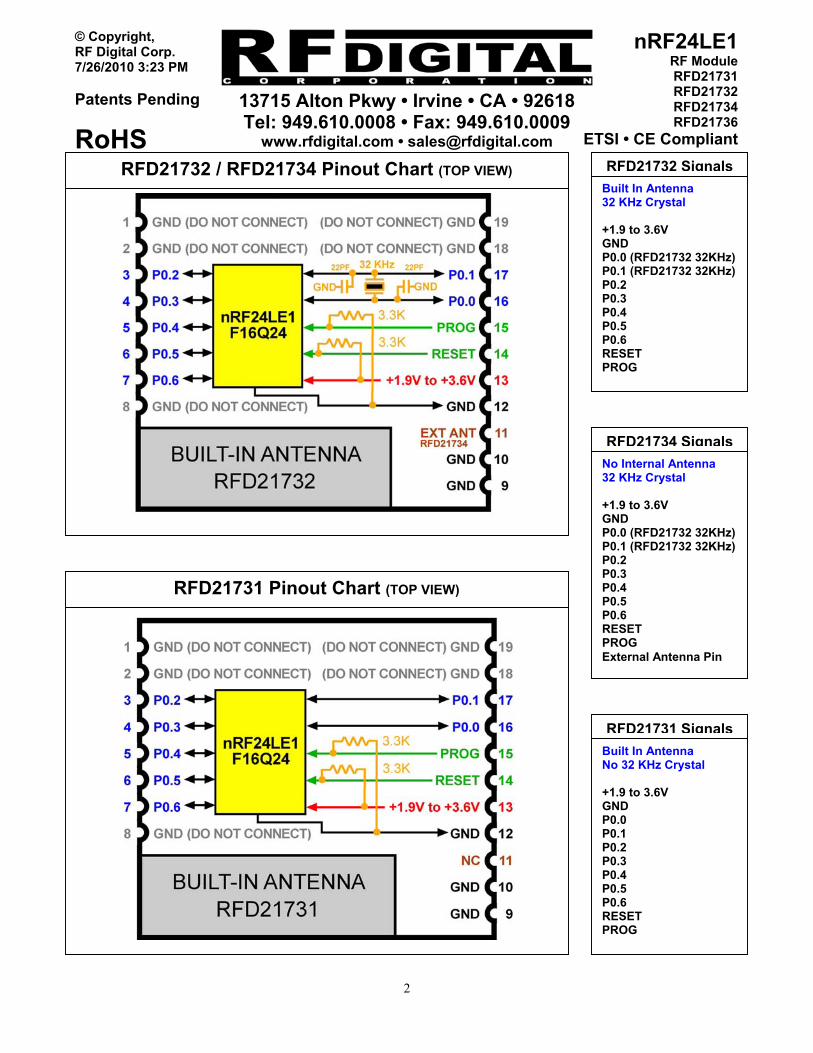
RFD21732 / RFD21734 Pinout Chart (TOP VIEW)
RFD21731 Pinout Chart (TOP VIEW)
Built In Antenna32 KHz Crystal +1.9 to 3.6V GND P0.0 (RFD21732 32KHz)P0.1 (RFD21732 32KHz)P0.2 P0.3 P0.4 P0.5 P0.6 RESET PROG
RFD21732 Signals
No Internal Antenna32 KHz Crystal +1.9 to 3.6V GND P0.0 (RFD21732 32KHz)P0.1 (RFD21732 32KHz)P0.2 P0.3 P0.4 P0.5 P0.6 RESET PROG External Antenna Pin
RFD21734 Signals
Built In AntennaNo 32 KHz Crystal +1.9 to 3.6V GND P0.0 P0.1 P0.2 P0.3 P0.4 P0.5 P0.6 RESET PROG
RFD21731 Signals

13715 Alton Pkwy • Irvine • CA • 92618 Tel: 949.610.0008 • Fax: 949.610.0009
www.rfdigital.com • [email protected]
3
nRF24LE1RF ModuleRFD21731RFD21732RFD21734RFD21736
ETSI • CE Compliant
© Copyright, RF Digital Corp. 7/26/2010 3:23 PM Patents Pending
RoHS
- NO RF parts or layout required, fully contained, easy access to all digital lines.- Typical outdoor range 300 feet (100 meters) - 125 channels, 2400 to 2525 MHz. - Current draw: 11.1 mA at 0 dBm Transmit, 13.3 mA at -94 dBm Receive. - Fully featured ultra low power nRF24L01+ 2.4GHz transceiver core - Worldwide 2.4GHz ISM band operation - Enhanced ShockBurstTM hardware link layer - 250 kbps, 1 Mbps and 2 Mbps on-air data rate options. - Air compatible with nRF24L01, nRF24L01+, nRF24LU1 and nRF2401A - Enhanced 8-bit 8051 compatible microcontroller - 32-bit multiplication-division unit - AES encryption/decryption accelerator - 16 kbytes on-chip flash memory - 1 kbyte on-chip data flash memory - 512 bytes high-endurance data flash memory - 1 kbyte on SRAM plus 256 bytes of IRAM - Low power 16MHz crystal and RC oscillators - Ultra low power 32kHz crystal and RC oscillators - Flexible real-time counter and three 16-bit timers/counters - Ultra low power analog comparator for system wake-up - Rich set of digital interfaces including: SPI master/slave, 2-wire master/slave, and UART - 2-channel PWM - Programmable resolution ADC: 6, 8, 10, or 12-bits - Random Number Generator based on thermal noise - 7 Programmable generic I/O pins
RFD21731, RFD21732, RFD21734 Features RF Digital's RFDP8 high level application protocol firmware which runs on the nRF24LE1-F16Q24 is available pre-loaded on the RFD21733 / RFD21735, ideal for those who don't have time to write code. So if you don’t want to do any development at all, then use RFD21733 / RFD21735 which are READY-TO-USE with its built-in user application interface (RFDP8). Includes RFID, Unique Electronic Serial Number, Logic Switch Transmitter / Receiver, Serial UART 9600-8N1 and many easy-to-use addressable network modes.
RFDP8 Option
RFD21736 Top View
RFD21736 Bottom View
RFD21736 Eval adaptor board for nRFgo Starter Kit The RFD21736 has a built-in RFD21731 and it plugs directly into Nordic's nRF6700 nRFgo Starter Kit board which is required to use the RFD21736. The RFD21736 has an on-board user switchable 32 KHz crystal, which allows evaluation of the RFD21732. (nRF6700 Required) You should ONLY use the RFD21736 and nRF6700 if you will be writing your own RF firmware, otherwise you should use the READY-TO-USE RFD21733, RFD21735, RFD21737.
+1.9 to 3.6VGND P0.0 Optional 32KHz P0.1 Optional 32KHz P0.2 P0.3 P0.4 P0.5 P0.6 RESET PROG With Switchable 32 KHz Crystal
Accessible PinsPlugs into MOD B (P4) on nRF6310 Nordic Dev. Board.
Plugs into MOD A (P3) on nRF6310 Nordic Dev. Board.
13715 Alton Pkwy • Irvine • CA • 92618 Tel: 949.610.0008 • Fax: 949.610.0009
www.rfdigital.com • [email protected]
4
nRF24LE1RF ModuleRFD21731RFD21732RFD21734RFD21736
ETSI • CE Compliant
© Copyright, RF Digital Corp. 7/26/2010 3:23 PM Patents Pending
RoHS a
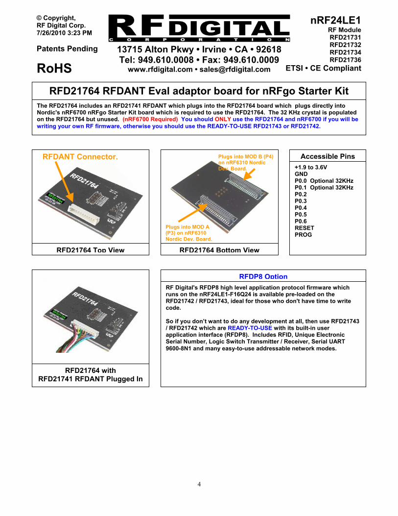
RFD21764 Top View
RFD21764 Bottom View
+1.9 to 3.6VGND P0.0 Optional 32KHz P0.1 Optional 32KHz P0.2 P0.3 P0.4 P0.5 P0.6 RESET PROG
Accessible PinsPlugs into MOD B (P4) on nRF6310 Nordic Dev. Board.
Plugs into MOD A (P3) on nRF6310 Nordic Dev. Board.
RFDANT Connector.
RFD21764 with RFD21741 RFDANT Plugged In
RFD21764 RFDANT Eval adaptor board for nRFgo Starter Kit The RFD21764 includes an RFD21741 RFDANT which plugs into the RFD21764 board which plugs directly into Nordic's nRF6700 nRFgo Starter Kit board which is required to use the RFD21764. The 32 KHz crystal is populated on the RFD21764 but unused. (nRF6700 Required) You should ONLY use the RFD21764 and nRF6700 if you will be writing your own RF firmware, otherwise you should use the READY-TO-USE RFD21743 or RFD21742.
RF Digital's RFDP8 high level application protocol firmware which runs on the nRF24LE1-F16Q24 is available pre-loaded on the RFD21742 / RFD21743, ideal for those who don't have time to write code. So if you don’t want to do any development at all, then use RFD21743 / RFD21742 which are READY-TO-USE with its built-in user application interface (RFDP8). Includes RFID, Unique Electronic Serial Number, Logic Switch Transmitter / Receiver, Serial UART 9600-8N1 and many easy-to-use addressable network modes.
RFDP8 Option
13715 Alton Pkwy • Irvine • CA • 92618 Tel: 949.610.0008 • Fax: 949.610.0009
www.rfdigital.com • [email protected]
5
nRF24LE1RF ModuleRFD21731RFD21732RFD21734RFD21736
ETSI • CE Compliant
© Copyright, RF Digital Corp. 7/26/2010 3:23 PM Patents Pending
RoHS
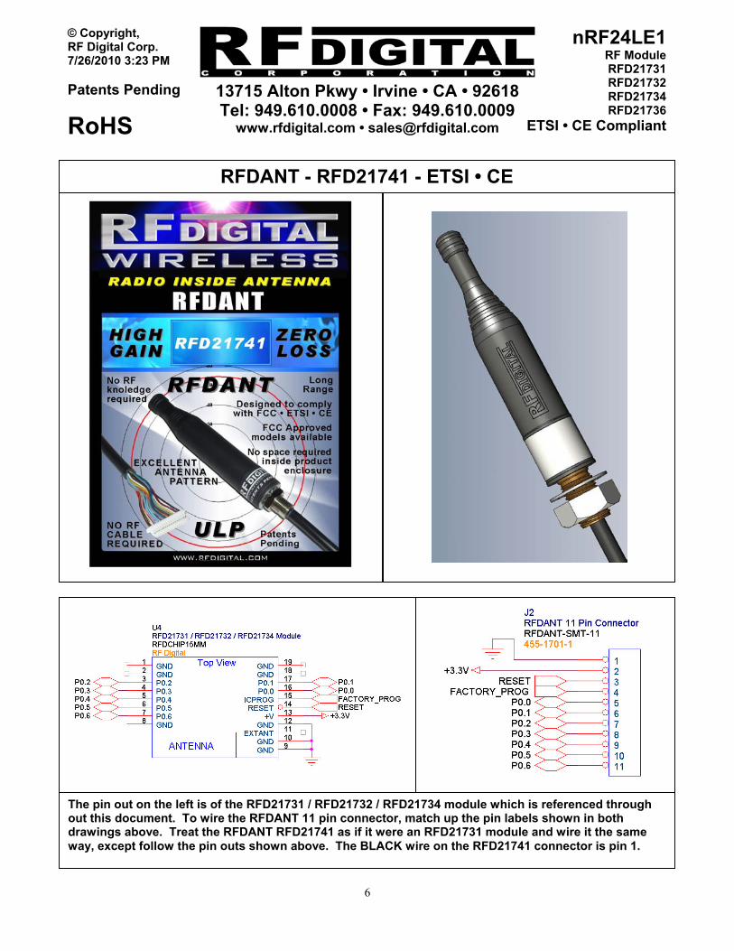
RFDANT - RFD21741 The RFD21741 RFDANT is a full nRF24LE1 2.4 GHz radio transceiver, completely built into an antenna form factor allowing the entire radio transceiver to be outside your product, were only the power and signal cable will extend into your product enclosure to then be connected to your PCB with a simple 1.5mm SMT or THROUGH HOLE connector. The RFD21741 RFDANT is currently available, as well as it's eval and programming board which is the RFD21764. The RFD21764 plugs into the Nordic nRFgo development board for programming and evaluation. The RFD21741 is functionally identical to the RFD21731 module and the RFD21764 works just like the RFD21736 eval board except it has an 11 pin 1.5mm connector on it so the RFDANT RFD21741 can plug into it for use with any other nRF24LE1 product running your own code. The RFD21741 has been range tested at 2,000 feet which is 4x the range of the RFD21731 which is at 500 feet. No special PCB layout is needed for the RFD21741, simply just put a connector on your PCB and you are done . All this substantial range increase is achieved all without any increase in current or battery consumption. The 2,000 foot range test was done using RF Digital's RFDP8 protocol running at 250 kbps and 0dbm power setting with the nRF24LE1.
The RFDANT is RF Digital's Worldwide Patent Pending Radio Inside Antenna product, which is a complete radio transceiver and antenna mounted inside of an antenna enclosure, suitable for mounting to virtually any type of end-product. The entire radio transceiver is mounted inside the antenna enclosure, so there is no loss of RF power to the antenna from the module, and results in the most effective power transfer ratio possible, providing lowest power consumption possible to achieve a specific range. The radio being inside of the antenna and outside the enclosure allows for more room inside the enclosure for the designers application electronics. Minimal interference with the internal electronics of the enclosure results in better range and performance of the wireless system. The actual effective antenna is pushed away from the enclosure, which reduces the effect of holding the enclosure, therefore improving the performance, range and predictability of the users wireless system. Logic level signals are used through an unshielded cable (not coax) to the RFDANT, which can be run for long distances without any loss to the performance of the wireless transceiver. By the antenna and module being fully outside allows for easy retrofit of nearly any product due to it not consuming any internal space inside the enclosure, drill a hole and screw it in, add a nut inside to secure it and wire the logic level signals to your electronics. Mount on metal or plastic enclosures with no worry about ground effects. Stable Antenna Pattern providing substantial, well-distributed, passive-gain for transmit and receive, results longer repeatable range from your wireless system.
13715 Alton Pkwy • Irvine • CA • 92618 Tel: 949.610.0008 • Fax: 949.610.0009
www.rfdigital.com • [email protected]
6
nRF24LE1RF ModuleRFD21731RFD21732RFD21734RFD21736
ETSI • CE Compliant
© Copyright, RF Digital Corp. 7/26/2010 3:23 PM Patents Pending
RoHS
RFDANT - RFD21741 - ETSI • CE
The pin out on the left is of the RFD21731 / RFD21732 / RFD21734 module which is referenced through out this document. To wire the RFDANT 11 pin connector, match up the pin labels shown in both drawings above. Treat the RFDANT RFD21741 as if it were an RFD21731 module and wire it the same way, except follow the pin outs shown above. The BLACK wire on the RFD21741 connector is pin 1.

13715 Alton Pkwy • Irvine • CA • 92618 Tel: 949.610.0008 • Fax: 949.610.0009
www.rfdigital.com • [email protected]
7
nRF24LE1RF ModuleRFD21731RFD21732RFD21734RFD21736
ETSI • CE Compliant
© Copyright, RF Digital Corp. 7/26/2010 3:23 PM Patents Pending
RoHS
Mating connectors for the 11 pin RFDANT connector, these part numbers can be found at Digikey in the USA http://www.digikey.com or at any other distributor. They are standard connectors and you may use other manufacturers as well. 1) Top Entry, Through Hole Type, 11 pos a. Digikey P/N 455-1666-ND b. Manufacturer P/N: B11B--ZR 2) Side Entry, Through Hole Type, 11 pos a. Digikey P/N 455-1678-ND b. Manufacturer P/N: S11B--ZR 3) Top Entry, SMT Type, 11 pos a. Digikey P/N 455-1690-2-ND b. Manufacturer P/N: B11B—ZR-SM4-TF 4) Side Entry, SMT Type, 11 pos a. Digikey P/N 455-1701-2-ND b. Manufacturer P/N: S11B—ZR-SM4-TF
RFDANT - RFD21741 Mating Connectors

13715 Alton Pkwy • Irvine • CA • 92618 Tel: 949.610.0008 • Fax: 949.610.0009
www.rfdigital.com • [email protected]
8
nRF24LE1RF ModuleRFD21731RFD21732RFD21734RFD21736
ETSI • CE Compliant
© Copyright, RF Digital Corp. 7/26/2010 3:23 PM Patents Pending
RoHS
-70
-60
-50
-40
-30
-201
2 34
56
7
8
9
10
11
12
13
14
15
16
17
18
19
20
21
22
2324
252627
282930
3132
33
34
35
36
37
38
39
40
41
42
43
44
45
46
47
48
49
5051
5253 54
Horizontal Antenna Pattern
-70
-60
-50
-40
-30
-201
2 3 4 5 67
89
1011
12131415161718
1920
2122
2324
252627282930
313233343536
3738
3940
4142
4344454647484950
5152
5354
5556 57 58 59 60
Vertical Antenna Pattern
RFDANT RFD21741 high performance antenna patterns are easily achieved without any RF considerations or knowledge because the 11 pin cable and connector only carries power and data signals so NO RF cable loss at all.

13715 Alton Pkwy • Irvine • CA • 92618 Tel: 949.610.0008 • Fax: 949.610.0009
www.rfdigital.com • [email protected]
9
nRF24LE1RF ModuleRFD21731RFD21732RFD21734RFD21736
ETSI • CE Compliant
© Copyright, RF Digital Corp. 7/26/2010 3:23 PM Patents Pending
RoHS
RFD21736 Schematic (plugs onto the nRF6310 eval board)
The 390k and 56k voltage devider sets a specific voltage which will be read by the programming board that tells it which of the three possible options of nRF24LE1 ICs are plugged into the nRF6310 development (programming) board. The RFD21736 has an RFD21731 mounted on it, which uses the 24 pin 4x4mm nRF24LE1 from Nordic, the other 2 options which it does not use are the 5mm and 7mm options. In the schematic above, P1 on the RFD21736 plugs into MOD A (P3) on the nRF6310 programming board. In the schematic above, P2 on the RFD21736 plugs into MOD B (P4) on the nRF6310 programming board. The Nordic nRF6310 development and programming board schematic is attached at the end of this document.

13715 Alton Pkwy • Irvine • CA • 92618 Tel: 949.610.0008 • Fax: 949.610.0009
www.rfdigital.com • [email protected]
10
nRF24LE1RF ModuleRFD21731RFD21732RFD21734RFD21736
ETSI • CE Compliant
© Copyright, RF Digital Corp. 7/26/2010 3:23 PM Patents Pending
RoHS
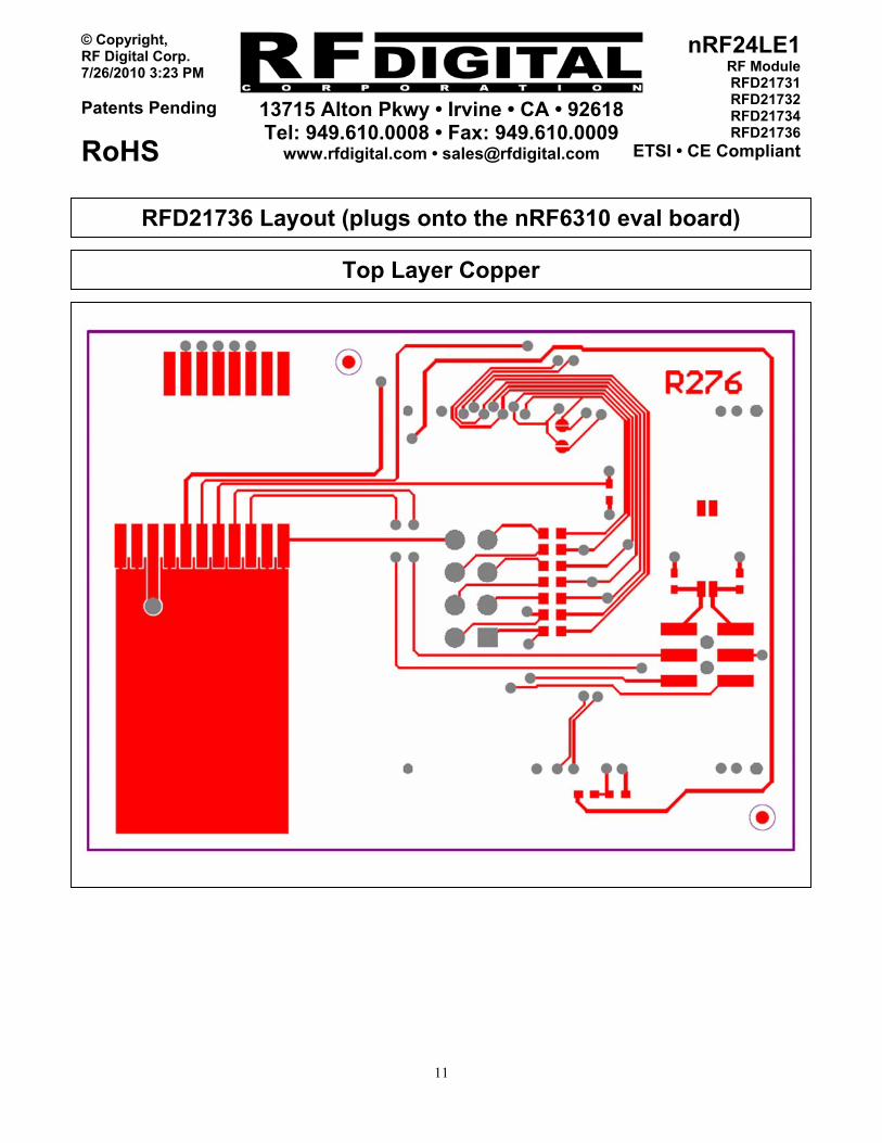
RFD21736 Layout (plugs onto the nRF6310 eval board)
Top Layer Silk Screen
13715 Alton Pkwy • Irvine • CA • 92618 Tel: 949.610.0008 • Fax: 949.610.0009
www.rfdigital.com • [email protected]
11
nRF24LE1RF ModuleRFD21731RFD21732RFD21734RFD21736
ETSI • CE Compliant
© Copyright, RF Digital Corp. 7/26/2010 3:23 PM Patents Pending
RoHS
RFD21736 Layout (plugs onto the nRF6310 eval board)
Top Layer Copper
13715 Alton Pkwy • Irvine • CA • 92618 Tel: 949.610.0008 • Fax: 949.610.0009
www.rfdigital.com • [email protected]
12
nRF24LE1RF ModuleRFD21731RFD21732RFD21734RFD21736
ETSI • CE Compliant
© Copyright, RF Digital Corp. 7/26/2010 3:23 PM Patents Pending
RoHS
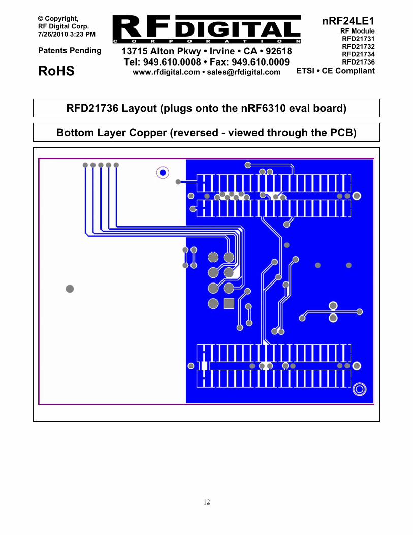
Bottom Layer Copper (reversed - viewed through the PCB)
RFD21736 Layout (plugs onto the nRF6310 eval board)

13715 Alton Pkwy • Irvine • CA • 92618 Tel: 949.610.0008 • Fax: 949.610.0009
www.rfdigital.com • [email protected]
13
nRF24LE1RF ModuleRFD21731RFD21732RFD21734RFD21736
ETSI • CE Compliant
© Copyright, RF Digital Corp. 7/26/2010 3:23 PM Patents Pending
RoHS
Bottom Layer Silk Screen (reversed - viewed through the PCB)
RFD21736 Layout (plugs onto the nRF6310 eval board)
13715 Alton Pkwy • Irvine • CA • 92618 Tel: 949.610.0008 • Fax: 949.610.0009
www.rfdigital.com • [email protected]
14
nRF24LE1RF ModuleRFD21731RFD21732RFD21734RFD21736
ETSI • CE Compliant
© Copyright, RF Digital Corp. 7/26/2010 3:23 PM Patents Pending
RoHS
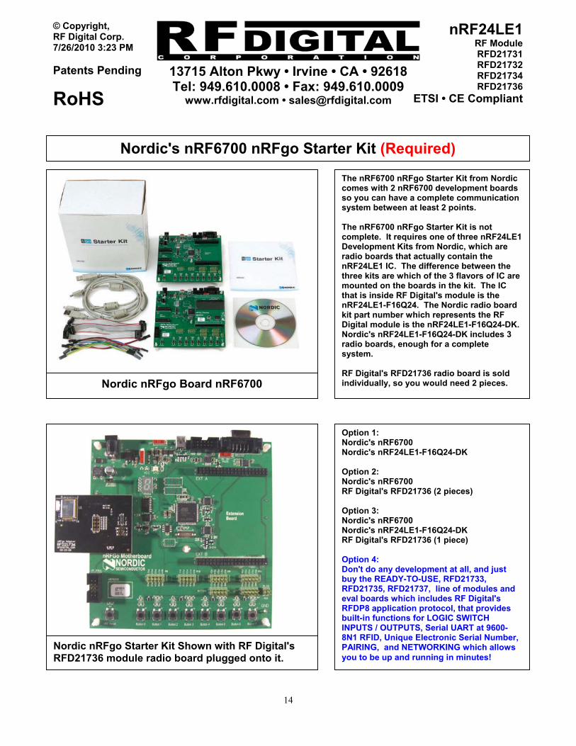
Nordic nRFgo Starter Kit Shown with RF Digital's RFD21736 module radio board plugged onto it.
Nordic nRFgo Board nRF6700
Nordic's nRF6700 nRFgo Starter Kit (Required)
The nRF6700 nRFgo Starter Kit from Nordic comes with 2 nRF6700 development boards so you can have a complete communication system between at least 2 points. The nRF6700 nRFgo Starter Kit is not complete. It requires one of three nRF24LE1 Development Kits from Nordic, which are radio boards that actually contain the nRF24LE1 IC. The difference between the three kits are which of the 3 flavors of IC are mounted on the boards in the kit. The IC that is inside RF Digital's module is the nRF24LE1-F16Q24. The Nordic radio board kit part number which represents the RF Digital module is the nRF24LE1-F16Q24-DK. Nordic's nRF24LE1-F16Q24-DK includes 3 radio boards, enough for a complete system. RF Digital's RFD21736 radio board is sold individually, so you would need 2 pieces.
Option 1:Nordic's nRF6700 Nordic's nRF24LE1-F16Q24-DK Option 2: Nordic's nRF6700 RF Digital's RFD21736 (2 pieces) Option 3: Nordic's nRF6700 Nordic's nRF24LE1-F16Q24-DK RF Digital's RFD21736 (1 piece) Option 4: Don't do any development at all, and just buy the READY-TO-USE, RFD21733, RFD21735, RFD21737, line of modules and eval boards which includes RF Digital's RFDP8 application protocol, that provides built-in functions for LOGIC SWITCH INPUTS / OUTPUTS, Serial UART at 9600-8N1 RFID, Unique Electronic Serial Number, PAIRING, and NETWORKING which allows you to be up and running in minutes!
13715 Alton Pkwy • Irvine • CA • 92618 Tel: 949.610.0008 • Fax: 949.610.0009
www.rfdigital.com • [email protected]
15
nRF24LE1RF ModuleRFD21731RFD21732RFD21734RFD21736
ETSI • CE Compliant
© Copyright, RF Digital Corp. 7/26/2010 3:23 PM Patents Pending
RoHS
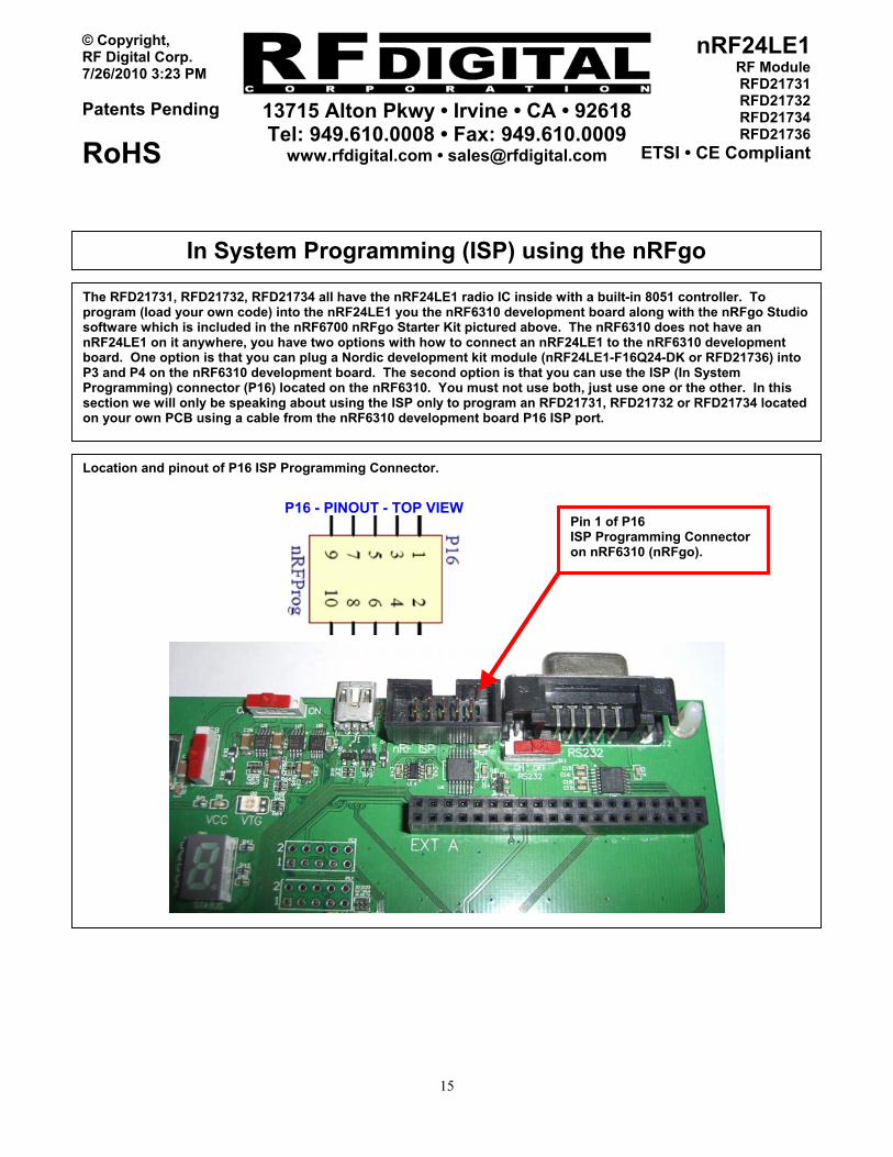
In System Programming (ISP) using the nRFgo
The RFD21731, RFD21732, RFD21734 all have the nRF24LE1 radio IC inside with a built-in 8051 controller. To program (load your own code) into the nRF24LE1 you the nRF6310 development board along with the nRFgo Studio software which is included in the nRF6700 nRFgo Starter Kit pictured above. The nRF6310 does not have an nRF24LE1 on it anywhere, you have two options with how to connect an nRF24LE1 to the nRF6310 development board. One option is that you can plug a Nordic development kit module (nRF24LE1-F16Q24-DK or RFD21736) into P3 and P4 on the nRF6310 development board. The second option is that you can use the ISP (In System Programming) connector (P16) located on the nRF6310. You must not use both, just use one or the other. In this section we will only be speaking about using the ISP only to program an RFD21731, RFD21732 or RFD21734 located on your own PCB using a cable from the nRF6310 development board P16 ISP port.
Location and pinout of P16 ISP Programming Connector.
P16 - PINOUT - TOP VIEWPin 1 of P16 ISP Programming Connector on nRF6310 (nRFgo).

13715 Alton Pkwy • Irvine • CA • 92618 Tel: 949.610.0008 • Fax: 949.610.0009
www.rfdigital.com • [email protected]
16
nRF24LE1RF ModuleRFD21731RFD21732RFD21734RFD21736
ETSI • CE Compliant
© Copyright, RF Digital Corp. 7/26/2010 3:23 PM Patents Pending
RoHS
Schematic - P16 section from nRF6310 development board

13715 Alton Pkwy • Irvine • CA • 92618 Tel: 949.610.0008 • Fax: 949.610.0009
www.rfdigital.com • [email protected]
17
nRF24LE1RF ModuleRFD21731RFD21732RFD21734RFD21736
ETSI • CE Compliant
© Copyright, RF Digital Corp. 7/26/2010 3:23 PM Patents Pending
RoHS
Blow is a copy from the Nordic nRF24LE1 data sheet version 1.4. Please refer to the Nordic data sheet for full details. This is only provided as a quick reference and not the information you should use for development.
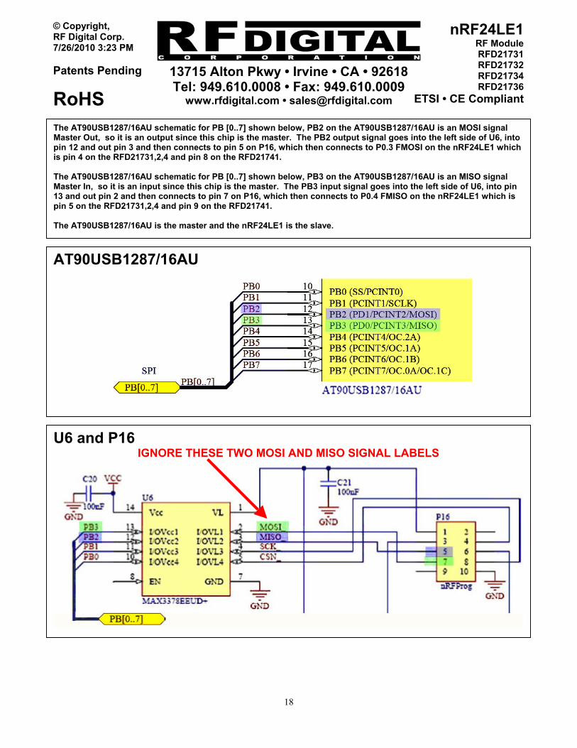
nRF24LE1-Q24 Pin Assignments
nRF24LE1-Q24 to nRFgo P16 MISO MOSI Interface Explanation Nordics nRFgo programming board uses an on-board AT90USB1287/16AU microcontroller to program the nRF24LE1-Q24 through a master-slave SPI communication using the MISO and MOSI lines on the AT90USB1287/16AU and the nRF24LE1-Q24. There are a set of pins required to perform the programming function and those pins are (in addition to power and ground): RST, PROG, SCN, SCK, MISO, MOSI. The RST, PROG, SCN and SCK signals are obvious they are outputs from the nRFgo programmer and inputs on the end of the nRF24LE1 module. However there are some easy mistakes that can be made with MISO and MOSI, so this is to explain detail about these two signals. The nRF24LE1-Q24 Pin Assignments image (above) shows P0.2, P0.3, P0.4, P0.5 which are SCK, MOSIM MISO, CSN respectfully. When the PROG pin is set to HIGH, those signals are called FSCN, FMISO, FMOSI, FSCK. They all have an "F" in front of them to indicate FLASH mode, which is only true when PROG line is high and SPI FLASH mode is entered. This means that on the nRF24LE1-Q24 FMISO which is P0.4 is an OUTPUT and FMOSI which is P0.3 is an INPUT. Continued on the next page…
13715 Alton Pkwy • Irvine • CA • 92618 Tel: 949.610.0008 • Fax: 949.610.0009
www.rfdigital.com • [email protected]
18
nRF24LE1RF ModuleRFD21731RFD21732RFD21734RFD21736
ETSI • CE Compliant
© Copyright, RF Digital Corp. 7/26/2010 3:23 PM Patents Pending
RoHS
U6 and P16 IGNORE THESE TWO MOSI AND MISO SIGNAL LABELS
AT90USB1287/16AU
The AT90USB1287/16AU schematic for PB [0..7] shown below, PB2 on the AT90USB1287/16AU is an MOSI signal Master Out, so it is an output since this chip is the master. The PB2 output signal goes into the left side of U6, into pin 12 and out pin 3 and then connects to pin 5 on P16, which then connects to P0.3 FMOSI on the nRF24LE1 which is pin 4 on the RFD21731,2,4 and pin 8 on the RFD21741. The AT90USB1287/16AU schematic for PB [0..7] shown below, PB3 on the AT90USB1287/16AU is an MISO signal Master In, so it is an input since this chip is the master. The PB3 input signal goes into the left side of U6, into pin 13 and out pin 2 and then connects to pin 7 on P16, which then connects to P0.4 FMISO on the nRF24LE1 which is pin 5 on the RFD21731,2,4 and pin 9 on the RFD21741. The AT90USB1287/16AU is the master and the nRF24LE1 is the slave.
13715 Alton Pkwy • Irvine • CA • 92618 Tel: 949.610.0008 • Fax: 949.610.0009
www.rfdigital.com • [email protected]
19
nRF24LE1RF ModuleRFD21731RFD21732RFD21734RFD21736
ETSI • CE Compliant
© Copyright, RF Digital Corp. 7/26/2010 3:23 PM Patents Pending
RoHS
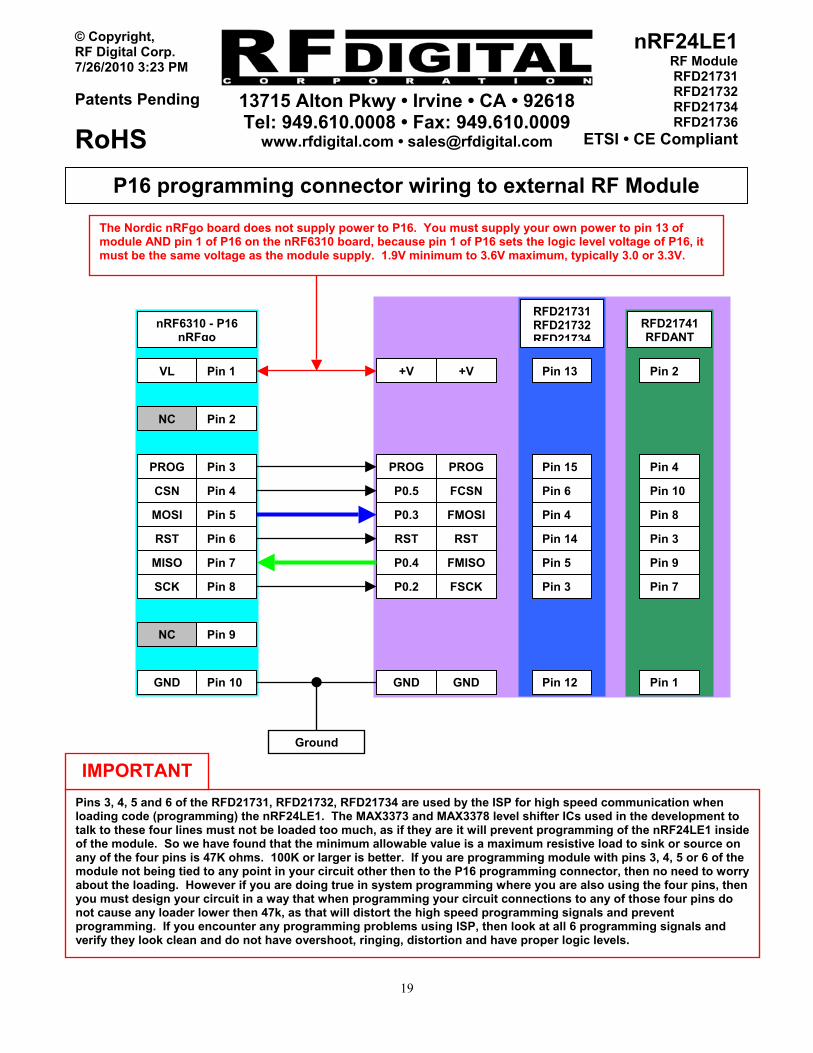
P16 programming connector wiring to external RF Module
NC Pin 2
PROG Pin 3 PROG Pin 15
CSN Pin 4 P0.5 Pin 6
MOSI Pin 5 P0.3 Pin 4
RST Pin 6 RST Pin 14
MISO Pin 7 P0.4 Pin 5
SCK Pin 8 P0.2 Pin 3
nRF6310 - P16 nRFgo
VL Pin 1 +V Pin 13
NC Pin 9
GND Pin 10 Pin 12
Ground
The Nordic nRFgo board does not supply power to P16. You must supply your own power to pin 13 of module AND pin 1 of P16 on the nRF6310 board, because pin 1 of P16 sets the logic level voltage of P16, it must be the same voltage as the module supply. 1.9V minimum to 3.6V maximum, typically 3.0 or 3.3V.
Pins 3, 4, 5 and 6 of the RFD21731, RFD21732, RFD21734 are used by the ISP for high speed communication when loading code (programming) the nRF24LE1. The MAX3373 and MAX3378 level shifter ICs used in the development to talk to these four lines must not be loaded too much, as if they are it will prevent programming of the nRF24LE1 insideof the module. So we have found that the minimum allowable value is a maximum resistive load to sink or source on any of the four pins is 47K ohms. 100K or larger is better. If you are programming module with pins 3, 4, 5 or 6 of the module not being tied to any point in your circuit other then to the P16 programming connector, then no need to worryabout the loading. However if you are doing true in system programming where you are also using the four pins, then you must design your circuit in a way that when programming your circuit connections to any of those four pins do not cause any loader lower then 47k, as that will distort the high speed programming signals and prevent programming. If you encounter any programming problems using ISP, then look at all 6 programming signals and verify they look clean and do not have overshoot, ringing, distortion and have proper logic levels.
IMPORTANT
+V
RFD21731 RFD21732 RFD21734
PROG
FCSN
FMOSI
RST
FMISO
FSCK
GND GND
RFD21741RFDANT
Pin 4
Pin 10
Pin 8
Pin 3
Pin 9
Pin 7
Pin 2
Pin 1

13715 Alton Pkwy • Irvine • CA • 92618 Tel: 949.610.0008 • Fax: 949.610.0009
www.rfdigital.com • [email protected]
20
nRF24LE1RF ModuleRFD21731RFD21732RFD21734RFD21736
ETSI • CE Compliant
© Copyright, RF Digital Corp. 7/26/2010 3:23 PM Patents Pending
RoHS
Overall Dimensions • Top View
Overall Dimensions • Side View

13715 Alton Pkwy • Irvine • CA • 92618 Tel: 949.610.0008 • Fax: 949.610.0009
www.rfdigital.com • [email protected]
21
nRF24LE1RF ModuleRFD21731RFD21732RFD21734RFD21736
ETSI • CE Compliant
© Copyright, RF Digital Corp. 7/26/2010 3:23 PM Patents Pending
RoHS
PCB Layout
13715 Alton Pkwy • Irvine • CA • 92618 Tel: 949.610.0008 • Fax: 949.610.0009
www.rfdigital.com • [email protected]
22
nRF24LE1RF ModuleRFD21731RFD21732RFD21734RFD21736
ETSI • CE Compliant
© Copyright, RF Digital Corp. 7/26/2010 3:23 PM Patents Pending
RoHS
RoHS Declaration Of Conformity
July 26, 2009
RF Digital declares that part numbers
• RFD21731 • RFD21732 • RFD21733 • RFD21734 • RFD21735 • RFD21736 • RFD21737 • RFD21738 • RFD21739 • RFD21740 • RFD21741 • RFD21742 • RFD21743 • RFD21764
are manufactured with RoHS materials.
13715 Alton Pkwy • Irvine • CA • 92618 Tel: 949.610.0008 • Fax: 949.610.0009
www.rfdigital.com • [email protected]
23
nRF24LE1RF ModuleRFD21731RFD21732RFD21734RFD21736
ETSI • CE Compliant
© Copyright, RF Digital Corp. 7/26/2010 3:23 PM Patents Pending
RoHS
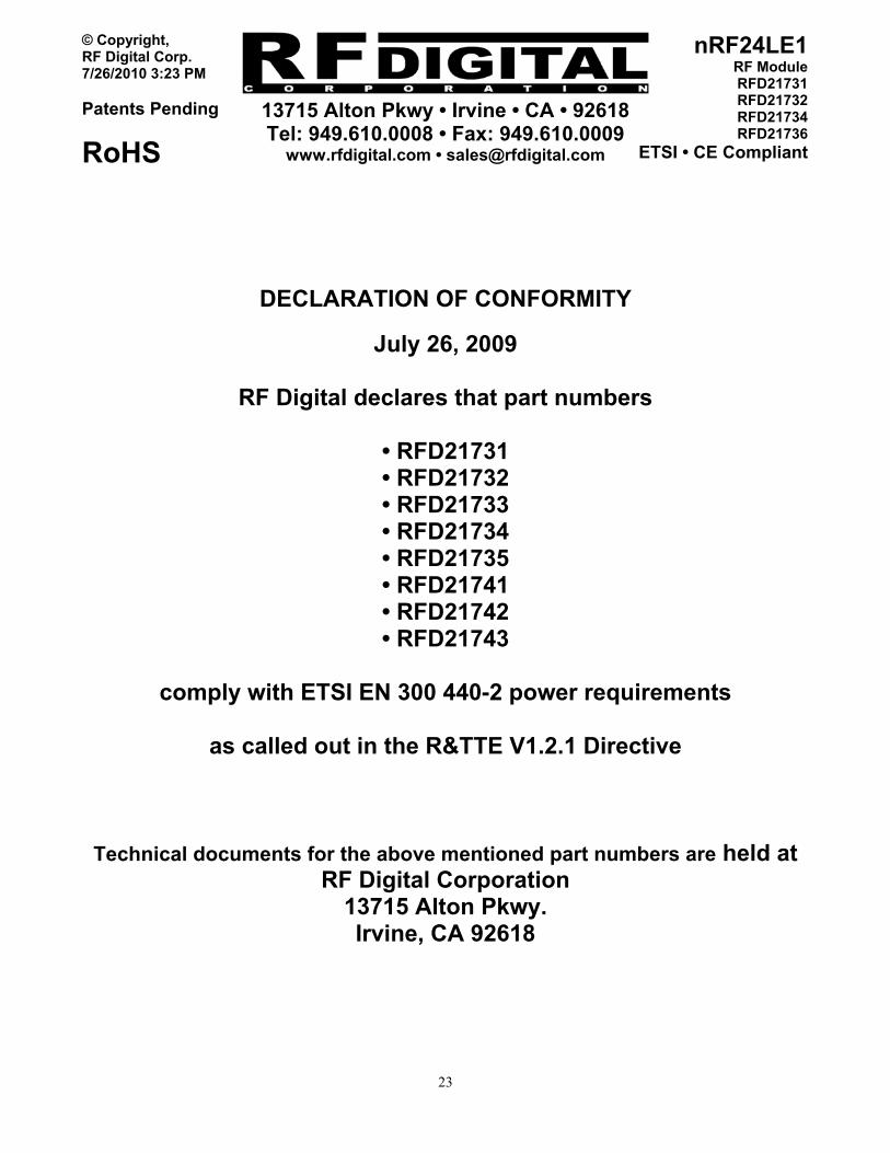
DECLARATION OF CONFORMITY
July 26, 2009
RF Digital declares that part numbers
• RFD21731 • RFD21732 • RFD21733 • RFD21734 • RFD21735 • RFD21741 • RFD21742 • RFD21743
comply with ETSI EN 300 440-2 power requirements
as called out in the R&TTE V1.2.1 Directive
Technical documents for the above mentioned part numbers are held at RF Digital Corporation
13715 Alton Pkwy. Irvine, CA 92618

13715 Alton Pkwy • Irvine • CA • 92618 Tel: 949.610.0008 • Fax: 949.610.0009
www.rfdigital.com • [email protected]
24
nRF24LE1RF ModuleRFD21731RFD21732RFD21734RFD21736
ETSI • CE Compliant
© Copyright, RF Digital Corp. 7/26/2010 3:23 PM Patents Pending
RoHS
The RFD21731, RFD21732 and RFD21734 are NOT washable. Use no-clean flux, leaded or lead-free. If you attempt to wash the modules, water will enter beneath (inside) the RF shield and get trapped, which may cause device failure or damage once powered on. There is no way to make sure all water has been removed before powering the module so do NOT wash the modules.
Washing
Do NOT pot or conformal coat the RFD21731, RFD21732 and RFD21734. If you plan on encapsulating the RFD21731, RFD21732 or RFD21734 in a potting compound or conformal coating, you must assure that the compound in liquid or solid form does not enter under the shield where there are sensitive RF components. Some of the capacitive values are as low as half a picofarad and sensitive to contacting materials such as potting compounds. There are potting compounds and conformal coatings which have very good dielectric constants and are suitable for 2.4 GHz potting applications, however, when you apply any of these, they were accounted for in the circuit design and might reduce performance of the device or all together cause it not to function. Applying any compound, conformal coating or potting directly to the module voids any and all warranty and support service. If your application requires 100% sealing of the module, there is a way to do this very successfully without impacting the module performance. Simply place the module on your PCB. Place a plastic cover over the module (like a hat), make the cover large enough to cover the whole module. Apply glue around the bottom perimeter of the cover where it sits on the PCB. This allows the module to function infree airspace while there is a complete seal around it. This information is only for reference and you should do your own testing with your application to find the best suitable fit for your own design.
Potting, Encapsulation and Conformal Coating
Use standard lead-free or leaded reflow profile for the RFD21731, RFD21732 and RFD21734. Your CM (Contract Manufacturer) should profile this module along with your PCB and all other parts on it through their reflow oven to properly set a profile suitable for all the parts on the board combined. If you are building a double sided placement board, place this device last so it will not be attempted to be reflowed upside-down. As with building any RF devices, you should always build a small quantity through your production process, test and verify, then increase your quantities to make sure the process is not harmful to the performance of your RF system. This is true with any RF system, including use of these modules.
Reflow Profile
13715 Alton Pkwy • Irvine • CA • 92618 Tel: 949.610.0008 • Fax: 949.610.0009
www.rfdigital.com • [email protected]
25
nRF24LE1RF ModuleRFD21731RFD21732RFD21734RFD21736
ETSI • CE Compliant
© Copyright, RF Digital Corp. 7/26/2010 3:23 PM Patents Pending
RoHS
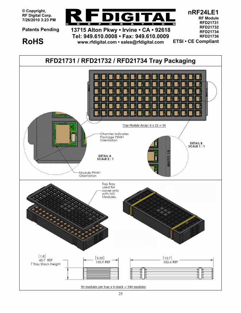
RFD21731 / RFD21732 / RFD21734 Tray Packaging

13715 Alton Pkwy • Irvine • CA • 92618 Tel: 949.610.0008 • Fax: 949.610.0009
www.rfdigital.com • [email protected]
26
nRF24LE1RF ModuleRFD21731RFD21732RFD21734RFD21736
ETSI • CE Compliant
© Copyright, RF Digital Corp. 7/26/2010 3:23 PM Patents Pending
RoHS
RFD21731 / RFD21732 / RFD21734 Tray Packaging

13715 Alton Pkwy • Irvine • CA • 92618 Tel: 949.610.0008 • Fax: 949.610.0009
www.rfdigital.com • [email protected]
27
nRF24LE1RF ModuleRFD21731RFD21732RFD21734RFD21736
ETSI • CE Compliant
© Copyright, RF Digital Corp. 7/26/2010 3:23 PM Patents Pending
RoHS
Important Notice RF Digital reserves the right to make corrections, modifications, and/or improvements to the product and/or its specifications at any time without notice. RF Digital assumes no liability for the user’s product and/or applications. RF Digital products are not authorized for use in safety-critical applications, including but not limited to life-support applications. RF Digital assumes no liability for parts or their application beyond replacement or refunding the original purchase price. All trademarks and trade names belong to their respective owners. End of Document.
RFD21731 / RFD21732 / RFD21734 Tray Packaging
13715 Alton Pkwy • Irvine • CA • 92618 Tel: 949.610.0008 • Fax: 949.610.0009
www.rfdigital.com • [email protected]
28
nRF24LE1RF ModuleRFD21731RFD21732RFD21734RFD21736
ETSI • CE Compliant
© Copyright, RF Digital Corp. 7/26/2010 3:23 PM Patents Pending
RoHS
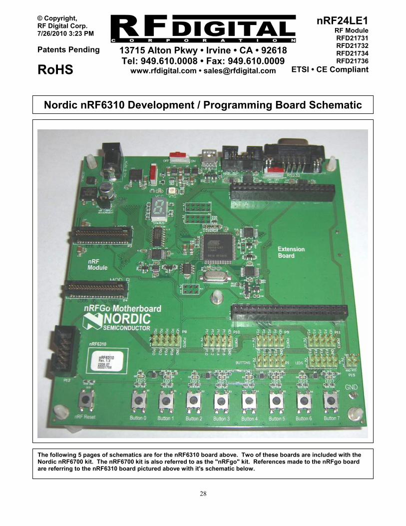
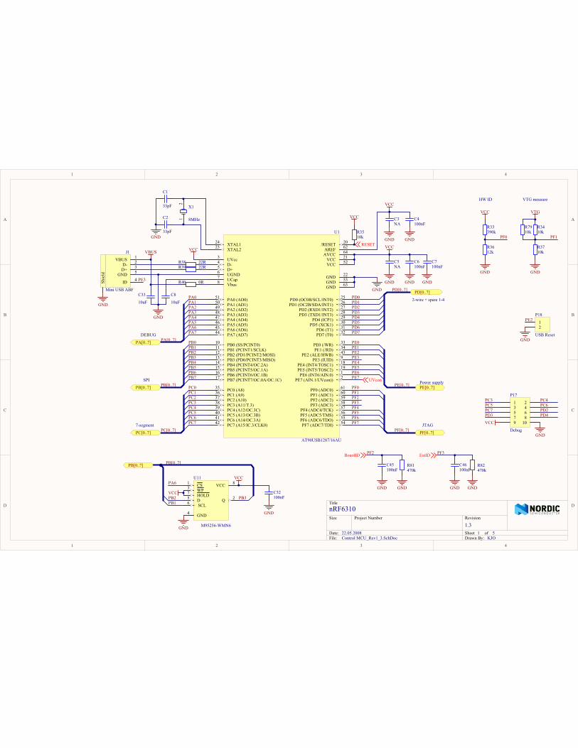
Nordic nRF6310 Development / Programming Board Schematic
The following 5 pages of schematics are for the nRF6310 board above. Two of these boards are included with the Nordic nRF6700 kit. The nRF6700 kit is also referred to as the "nRFgo" kit. References made to the nRFgo board are referring to the nRF6310 board pictured above with it's schematic below.
1
1
2
2
3
3
4
4
D D
C C
B B
A A
Title
Size Project Number
Date:File:
Sheet ofDrawn By:
Revision
nRF6310
1.322.05.2008Control MCU_Rev1_3.SchDoc
1 5KJO
AT90USB1287/16AU
PA7 (AD7)44 PA6 (AD6)45 PA5 (AD5)46 PA4 (AD4)47 PA3 (AD3)48 PA2 (AD2)49 PA1 (AD1)50 PA0 (AD0)51
PB0 (SS/PCINT0)10
PB1 (PCINT1/SCLK)11
PB2 (PD1/PCINT2/MOSI)12
PB3 (PD0/PCINT3/MISO)13
PB4 (PCINT4/OC.2A)14
PB5 (PCINT5/OC.1A)15
PB6 (PCINT6/OC.1B)16
PB7 (PCINT7/OC.0A/OC.1C)17
PC0 (A8)35
PC1 (A9)36
PC2 (A10)37
PC3 (A11/T.3)38
PC4 (A12/OC.3C)39
PC5 (A13/OC.3B)40
PC6 (A14/OC.3A)41
PC7 (A15/IC.3/CLK0)42
PD0 (OC0B/SCL/INT0) 25
PD1 (OC2B/SDA/INT1) 26
PD2 (RXD1/INT2) 27
PD3 (TXD1/INT3) 28
PD4 (ICP1) 29
PD5 (XCK1) 30
PD6 (T1) 31
PD7 (T0) 32
PE0 (/WR) 33
PE1 (/RD) 34
PE2 (ALE/HWB) 43
PE3 (IUID) 9
PE4 (INT4/TOSC1) 18
PE5 (INT5/TOSC2) 19
PE6 (INT6/AIN.0) 1
PE7 (AIN.1/UVcon)) 2
PF7 (ADC7/TDI) 54PF6 (ADC6/TDO) 55PF5 (ADC5/TMS) 56PF4 (ADC4/TCK) 57PF3 (ADC3) 58PF2 (ADC2) 59PF1 (ADC1) 60PF0 (ADC0) 61
D-4
D+5
UGND6
UCap7
Vbus8
/RESET 20
VCC 21
GND 22
XTAL223 XTAL124
VCC 52
GND 53
AREF 62
GND 63
AVCC 64
UVcc3
U1
22RR3822RR39
VBUS
GND
33pF
C1
33pF
C2
GND
VCCVCC
GND
0RR40
PA0PA1PA2PA3PA4PA5PA6PA7
PB0
PB4PB5PB6PB7
PD0PD1PD2PD3PD4PD5PD6PD7
PF0PF1
PF4PF5PF6PF7
PB1PB2PB3
NAC5
GND
10kR34
10kR37
GND
VTG
390kR33
12kR36
GND
VCC
VTG measureHW IDVCC
NAC3
GND
PB[0..7]
PF[0..7]
PF0 PF1
PB[0..7]
PF[0..7]
10kR35
VCC
PD[0..7] PD[0..7]
100nFC6
100nFC7
GND GND
100nFC4
GND
PA[0..7] PA[0..7]DEBUG
SPI
JTAG
2-wire + spare 1-4
BoardID
RESET
ExtID
CS1
Q 2
WP3
GND4
D5
SCL6
HOLD7
VCC 8
M95256-WMN6
U11 VCC
100nFC32
GND
PA6
PB2PB1
PB3
GND
VCC
PB[0..7] PB[0..7]
UVcon
PC0PC1PC2PC3PC4PC5PC6PC7
Power supply
PE0PE1
PE3PE4PE5PE6
PE[0..7]PE[0..7]
PE2
VBUS 1
D- 2
D+ 3
GND 5
ID 4Shield
J1
Mini USB ABF
GND
PE3
10uF
C8
10uF
C33
10kR79
12
8MHz
X1
PC[0..7]
7-segment
1 23 45 67 89 10
P17
Debug
PC3PC5PC7PD3
PC4PC6PD2
GND
VCC
PC[0..7]
PD4
12
P18
USB ResetGND
PE2
PF2 PF3
PF2PF3
100nFC45
100nFC46
GND GND
470kR81
470kR82
GNDGND
PE7

1
1
2
2
3
3
4
4
5
5
6
6
7
7
8
8
D D
C C
B B
A A
Title
Size Project Number
Date:File:
Sheet ofDrawn By:
Revision
nRF6310
1.322.05.2008Extension_Rev1_3.SchDoc
2 5KJO
ProjectNumber
1 23 45 67 89 1011 1213 1415 1617 1819 2021 2223 2425 2627 2829 3031 3233 3435 3637 3839 40
P3
GND GND
1 23 45 67 89 1011 1213 1415 1617 1819 2021 2223 2425 2627 2829 3031 3233 3435 3637 3839 40
P6
GND GND
VTG
Devicepo
rts
1 23 45 67 89 10
P8nRF P0.1nRF P0.3nRF P0.5nRF P0.7
nRF P0.0nRF P0.2nRF P0.4nRF P0.6
GND
VEXT
1 23 45 67 89 10
P10nRF P1.1nRF P1.3nRF P1.5nRF P1.7
nRF P1.0nRF P1.2nRF P1.4nRF P1.6
GND
VEXT
Q6BC847C
10k
R56
10kR59
GND
VCC VEXT
MISO
SCKCSN
PB3PB2PB1PB0
PB5PB6
PB[0..7]
PB[0..7
]
PB7
Q5BC847C
GND
10k
R51
10kR58
SCL
SDA
Spare1Spare2
PD0
PD1
PD2PD3
PD7
VCC VEXT
PD[0..7
]
PD[0..7]
1 23 45 67 89 1011 1213 1415 1617 1819 2021 2223 2425 2627 2829 3031 3233 3435 3637 3839 40
P4
GND GND
1 23 45 67 89 10
P9nRF P2.1nRF P2.3nRF P2.5nRF P2.7
nRF P2.0nRF P2.2nRF P2.4nRF P2.6
GND
VEXT
1 23 45 67 89 10
P11nRF P3.1nRF P3.3nRF P3.5nRF P3.7
nRF P3.0nRF P3.2nRF P3.4nRF P3.6
GND
VEXT
1 23 45 67 89 1011 1213 1415 1617 1819 2021 2223 2425 2627 2829 3031 3233 3435 3637 3839 40
P5
GND GND
VCC VTG'
1 23 45 67 89 10
P12
nRF RST
TCKTDOTMS
TDI
GND
VEXT
Exp
ansion
ports
100nFC11
100nFC12
GNDGND
100nFC10
GND100nF
C9
GND
VTG' VTG
12P7Jumper
Closed for normal operationOpen for current measurements
PD4PD5
Spare3Spare4
Port0
Port1
Port2
Port3
nRF Debug/JTAG
MOD A MOD B EXT A EXT B
10kR53
10kR54
VEXT
10kR55
10kR52
VCCVCC
GND
10k
R50
150R
R49
VEXT
S10
nRFRST
ModuleReset
nRF P0.0nRF P0.2nRF P0.4nRF P0.6
nRF P1.0nRF P1.2nRF P1.4nRF P1.6
nRF P0.1nRF P0.3
nRF P0.7nRF P0.5
nRF P1.1nRF P1.3nRF P1.5nRF P1.7
PROG nRF RST
GND GNDMOSI MISOCSN SCK
SCL SDAGND GND
Spare1
GNDGND
Spare2nRF P2.0nRF P2.2nRF P2.4nRF P2.6
nRF P3.0nRF P3.2nRF P3.4nRF P3.6
nRF P2.1nRF P2.3nRF P2.5nRF P2.7
nRF P3.1nRF P3.3nRF P3.5nRF P3.7
GND GND
GND GND
GND GND
TCKTDI
TDOTMS
Spare3 Spare4
VEXT
Q7BC847C
GND
10kR57
10kR60
GND
VCC
VEXT
TCKTDOTDITMS
nRF RST
PA[0..7]
PA[0..7
]
100nFC13
100nFC14
GND
GNDPA0PA1PA2PA3
MOSI
PROG
PA7
ExtIDGND GND
VCC VTG'
nRF P0.0nRF P0.2nRF P0.4nRF P0.6
nRF P1.0nRF P1.2nRF P1.4nRF P1.6
nRF P0.1nRF P0.3
nRF P0.7nRF P0.5
nRF P1.1nRF P1.3nRF P1.5nRF P1.7
PROG nRF RST
GND GNDMOSI MISOCSN SCK
SCL SDAGND GND
Spare1
GNDGND
Spare2
VTG
nRF P2.0nRF P2.2nRF P2.4nRF P2.6
nRF P3.0nRF P3.2nRF P3.4nRF P3.6
nRF P2.1nRF P2.3nRF P2.5nRF P2.7
nRF P3.1nRF P3.3nRF P3.5nRF P3.7
GND GND
GND GND
GND GND
TCKTDI
TDOTMS
Spare3 Spare4
BoardIDGND GND
VEXT
VEXT will be connected toVTG or VCC on the plug-inmodule
BoardID BoardID
ExtID ExtID
VEXT
100nFC36
GND
PD6
GNDGND
FDV304PQ1110kR78
FDV301NQ13
FDV301NQ12
VEXT
GND
VEXT VEXT
GND
Q14BC847C
10kR77
10kR80
GND
PB4
VEXT GND
VCC
100nFC41
VEXT
100nFC42
GNDGND
MAX3378EEUD+
I/OVL1 2
I/OVL2 3
I/OVL3 4
VL 1
EN8
I/OVL4 5I/OVcc410
GND 7
Vcc14
I/OVcc311 I/OVcc212 I/OVcc113
U3
MAX3378EEUD+
I/OVL1 2
I/OVL2 3
I/OVL3 4
VL 1
EN8
I/OVL4 5I/OVcc410
GND 7
Vcc14
I/OVcc311 I/OVcc212 I/OVcc113
U4
MAX3378EEUD+
I/OVL1 2
I/OVL2 3
I/OVL3 4
VL 1
EN8
I/OVL4 5I/OVcc410
GND 7
Vcc14
I/OVcc311 I/OVcc212 I/OVcc113
U2
I/OVcc21
GND 2
VL
3
I/OVL2 4I/OVcc18
Vcc
7
EN 6
I/OVL1 5
U13
MAX3373EEKA+

1
1
2
2
3
3
4
4
5
5
6
6
7
7
8
8
D D
C C
B B
A A
Title
Size Project Number
Date:File:
Sheet ofDrawn By:
Revision
nRF6310
1.322.05.2008Interfaces_Rev1_3.SchDoc
3 5KJO
ProjectNumber
13
10
11
8
12
9
14
7
C1+1
C2+4
GND15
C1-3 VCC 16
C2-5
V- 6
V+ 2
U5
MAX3232CUE
100nF
C16
100nF
C19
100nFC15
100nFC18 GND
GND
VEXT
100nFC17
GND1
2
3
4
5
6
7
8
9
11
10
9 Pin Dsub Female
J2
GND
GND
RS232
TXD
RXD
GND
Q8BC847C
GND
10kR61
10kR62
GND
VCC
MOSI_MISO_SCK_CSN_
PROG_RST_
PB3PB2PB1PB0
PB5PB6
PB[0..7]
PB[0..7
]
1 23 45 67 89 10
P16
GND
100nFC21
GND
100nF
C20
GND
VCC
GND
PB3PB1 PB2
PB[0..7] PB[0..7]
RESET
1 23 45 6
P141 23 45 67 89 10
P13
VCC
PF4PF6PF5
PF7
PF[0..7] PF[0..7]
RESET
GNDISP Atmel MCU JTAG Atmel MCU
nRFProg
The device to be programmedwill supply U5 and U14 withthe correct voltage for logiclevel shifting.
23
1 S11
H1
Hole
H2
Hole
H3
Hole
H4
Hole
GND GND GND GND
H5
Hole
GND
G1
Ground connection
GND
f 2
g 3
e 4d 5
K9
c 8
DP 6
b 10a 1
DP7
HDSP-U503
DS1
GND
150RR41150RR42150RR43150RR44150RR45150RR46150RR47150RR48
GND
GNDOE 13
RCLK 12
SER 14
SRCLR 10
SRCLK 11
QA15
QB1
QC2
QD3
QE4
QF5
QG6
QH7
QH'9
VCC16
GND 8
74HC595D
U12
100nF
C35
VCC
GND
PC[0..7]GND
PC2
PC1
PC0
Load
Clock
Data
PC[0..7]
RTS
CTS
1 23 4
P15
Header 2X2
VCC
MAX3378EEUD+
I/OVL1 2
I/OVL2 3
I/OVL3 4
VL 1
EN8
I/OVL4 5I/OVcc410
GND 7
Vcc14
I/OVcc311 I/OVcc212 I/OVcc113
U6
VCC100nFC44
GND
GND
100nFC43
GND
I/OVcc21
GND 2
VL
3
I/OVL2 4I/OVcc18
Vcc
7
EN 6
I/OVL1 5
U14
MAX3373EEKA+
PA[0..7] PA[0..7]
PA5
1
1
2
2
3
3
4
4
D D
C C
B B
A A
Title
Size Project Number
Date:File:
Sheet ofDrawn By:
Revision
nRF6310
1.322.05.2008Power supply_Rev1_3.SchDoc
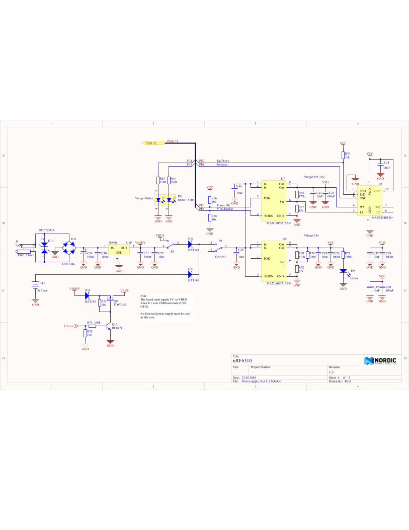
4 5KJO
MAX1806EUA33+
In1
In2
POK3
/SHDN4 GND 5
Set 6
Out 7Out 8U7
15kR67
470kR65
MAX5454EUB+
/CS11
U/D2 VDD
3
W14
L15 L2 6W2 7
GND
8
/INC9
/CS2 10
U8
GND
MAX1806EUA33+
In1
In2
POK3
/SHDN4 GND 5
Set 6
Out 7Out 8U9
GND
GND
22kR72
470kR69
100kR70
VCC
VTG
GND
GND
Vtarget 0.9-3.6v
Vfixed 3.8v
10kR66
VCC
VCC
150RR71
GND3xAAA
BT1
GND
23
1 S9
VBUS
DBS104G
D11
GND 100uFC26
GND
IN1
4
OUT 3
GND
U1078M05
GND
D12
BAT165
D13
BAT165
100nFC30
100nFC31
GND GND GND GND
GND
PE[0..7] PE[0..7]
VTG EnablePower OK
IncreaseUp/Down
PE0
PE1PE2
PE6
150RR64
150RR63
PE5PE4
12
34
GR
HSMF-A203D8
D9
Green
100nFC24
GND
100nFC25
GND
123
PWR 2.1mm
J3
12
D10
SM6T27CA
Vtarget Status
23
1
S8
10kR68
GND
GND
ON/OFF
GND GND
VBUS
100nF
C34
GND
VTG'
GND
100nFC38
GND
VCC
GND
100nFC40
GND
UVcon
10uFC27
10uF
C22
10uF
C28
10uFC23
10uFC29
10uFC37
10uFC39
VDD5V
FDV304PQ9
VDD5V
Q10BC847C
10kR73
GND
100kR74
10kR75
GND
Note:The board must supply 5V to VBUSwhen U1 is in USB host mode (USBOTG).
An External power supply must be usedin this case.
10kR76
VCC
D14
BAT165

1
1
2
2
3
3
4
4
D D
C C
B B
A A
Title
Size Project Number
Date:File:
Sheet ofDrawn By:
Revision
nRF6310
1.322.05.2008Buttons LEDs_Rev1_3.SchDoc
5 5KJO
S0
GND
10k
R18
150R
R17
VEXT
GND
10k
R20
150R
R19
GND
10k
R22
150R
R21
GND
10k
R24
150R
R23
GND
10k
R26
150R
R25
GND
10k
R28
150R
R27
GND
10k
R30
150R
R29
GND
10k
R32
150R
R31
1 23 45 67 89 10
P1
GND
150RR2
VCC VCC
150RR4
4.7kR1
GND GND
4.7kR3
150RR6
VCC VCC
150RR8
4.7kR5
GND GND
4.7kR7
150RR10
VCC VCC
150RR12
4.7kR9
GND GND
4.7kR11
150RR14
VCC VCC
150RR16
4.7kR13
GND GND
4.7kR15
1 23 45 67 89 10
P2
GND
Q1ABC847BS
Q3BBC847BS
Q3ABC847BS
Q1BBC847BS
Q4ABC847BS
Q2BBC847BS
Q2ABC847BS
Q4BBC847BS
D0 D2 D4 D6 D7 D5 D3 D1
S2 S4 S6 S7 S5 S3 S1
Buttons LEDs
VEXT VEXT VEXT VEXT VEXT VEXT VEXT

13715 Alton Pkwy • Irvine • CA • 92618 Tel: 949.610.0008 • Fax: 949.610.0009 www.rfdigital.com • [email protected]
For free RF layout design reviews, send color screen captures of your layout to [email protected], you will save time and money before you fabricate your boards.
We are always here to support you!
1
© Copyright, RF Digital Corp. 7/25/2010 11:04 AM Patents Pending
RoHS RFD21733 FCC APPROVED
Layout ExamplesRFDANT RF ModuleRFD21743 RFD21731RFD21741 RFD21732
RFD21733RFD21734RFD21735
ETSI • CE Compliant
Surface Mounted RF Module Layout Examples
For Part Numbers RFD21731, RFD21732, RFD21733, RFD21734, RFD21735
Go to http://www.rfdigital.com for complete data sheet.
For free RF layout design reviews, send color screen captures of your layout to [email protected], you will save time and money before you fabricate your boards.
We are always here to support you!
For use with
External Antenna
RFD21735 / RFD21734
21733 FCC Approved - Built-In Antenna
RFD21731 / RFD21732 / RFD21733
21731 / 21732 / 21733 / 21734 / 21735
Please use the legend below to identify the colors, objects and their meanings in this document.
Legend
13715 Alton Pkwy • Irvine • CA • 92618 Tel: 949.610.0008 • Fax: 949.610.0009 www.rfdigital.com • [email protected]
For free RF layout design reviews, send color screen captures of your layout to [email protected], you will save time and money before you fabricate your boards.
We are always here to support you!
2
© Copyright, RF Digital Corp. 7/25/2010 11:04 AM Patents Pending
RoHS RFD21733 FCC APPROVED
Layout ExamplesRFDANT RF ModuleRFD21743 RFD21731RFD21741 RFD21732
RFD21733RFD21734RFD21735
ETSI • CE Compliant
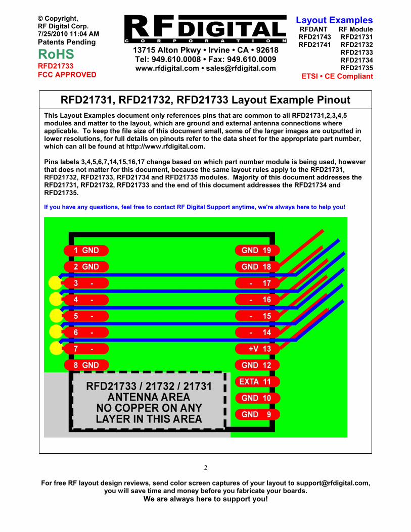
This Layout Examples document only references pins that are common to all RFD21731,2,3,4,5 modules and matter to the layout, which are ground and external antenna connections where applicable. To keep the file size of this document small, some of the larger images are outputted in lower resolutions, for full details on pinouts refer to the data sheet for the appropriate part number, which can all be found at http://www.rfdigital.com. Pins labels 3,4,5,6,7,14,15,16,17 change based on which part number module is being used, however that does not matter for this document, because the same layout rules apply to the RFD21731, RFD21732, RFD21733, RFD21734 and RFD21735 modules. Majority of this document addresses the RFD21731, RFD21732, RFD21733 and the end of this document addresses the RFD21734 and RFD21735. If you have any questions, feel free to contact RF Digital Support anytime, we're always here to help you!
RFD21731, RFD21732, RFD21733 Layout Example Pinout
13715 Alton Pkwy • Irvine • CA • 92618 Tel: 949.610.0008 • Fax: 949.610.0009 www.rfdigital.com • [email protected]
For free RF layout design reviews, send color screen captures of your layout to [email protected], you will save time and money before you fabricate your boards.
We are always here to support you!
3
© Copyright, RF Digital Corp. 7/25/2010 11:04 AM Patents Pending
RoHS RFD21733 FCC APPROVED
Layout ExamplesRFDANT RF ModuleRFD21743 RFD21731RFD21741 RFD21732
RFD21733RFD21734RFD21735
ETSI • CE Compliant
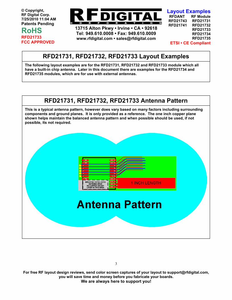
The following layout examples are for the RFD21731, RFD21732 and RFD21733 module which all have a built-in chip antenna. Later in this document there are examples for the RFD21734 and RFD21735 modules, which are for use with external antennas.
RFD21731, RFD21732, RFD21733 Layout Examples
This is a typical antenna pattern, however does vary based on many factors including surrounding components and ground planes. It is only provided as a reference. The one inch copper plane shown helps maintain the balanced antenna pattern and when possible should be used, if not possible, its not required.
RFD21731, RFD21732, RFD21733 Antenna Pattern

13715 Alton Pkwy • Irvine • CA • 92618 Tel: 949.610.0008 • Fax: 949.610.0009 www.rfdigital.com • [email protected]
For free RF layout design reviews, send color screen captures of your layout to [email protected], you will save time and money before you fabricate your boards.
We are always here to support you!
4
© Copyright, RF Digital Corp. 7/25/2010 11:04 AM Patents Pending
RoHS RFD21733 FCC APPROVED
Layout ExamplesRFDANT RF ModuleRFD21743 RFD21731RFD21741 RFD21732
RFD21733RFD21734RFD21735
ETSI • CE Compliant
When placing the module info a plastic enclosure, it is highly recommended that you locate the module in the corner of the enclosure / PCB so it will be as far away from your other components on the PCB and as close to free airspace as possible. In addition, you want to locate the module in a position in your product where it will have as much free airspace as possible near the antenna when in use. For example if it will be placed against a wall, it is preferred to locate the module so it will be in a location in your product where it will be on the side of the product where it will be further away from the wall, rather then directly next to it, so the RF signal can have as much free airspace to give you the best range performance possible. (Note: If you plan on using a metal enclosure, you can not locate the module inside of the enclosure or it will have very limited range, for metal enclosures we recommend the RFD21743 which is specifically suited for that.) The electrical ground connection to the module is to be made with a thin trace so the one inch ground plane off to the side can be effective.
RF Signals in this area. If you place anything such as components, wires, metal parts of any type in this area, it will block the RF signals and drastically limit your range. Leave this area open.
RFD21731, RFD21732, RFD21733 Keep Out Area - Example 1
13715 Alton Pkwy • Irvine • CA • 92618 Tel: 949.610.0008 • Fax: 949.610.0009 www.rfdigital.com • [email protected]
For free RF layout design reviews, send color screen captures of your layout to [email protected], you will save time and money before you fabricate your boards.
We are always here to support you!
5
© Copyright, RF Digital Corp. 7/25/2010 11:04 AM Patents Pending
RoHS RFD21733 FCC APPROVED
Layout ExamplesRFDANT RF ModuleRFD21743 RFD21731RFD21741 RFD21732
RFD21733RFD21734RFD21735
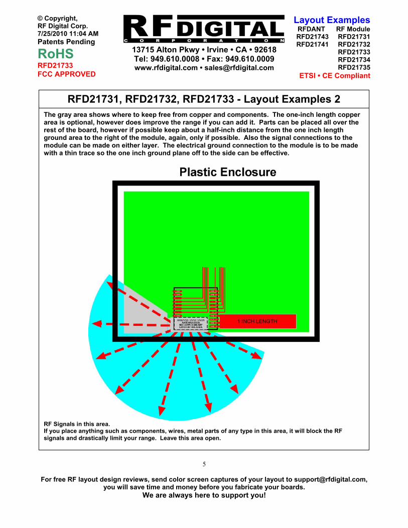
ETSI • CE Compliant
The gray area shows where to keep free from copper and components. The one-inch length copper area is optional, however does improve the range if you can add it. Parts can be placed all over the rest of the board, however if possible keep about a half-inch distance from the one inch length ground area to the right of the module, again, only if possible. Also the signal connections to the module can be made on either layer. The electrical ground connection to the module is to be made with a thin trace so the one inch ground plane off to the side can be effective.
RF Signals in this area. If you place anything such as components, wires, metal parts of any type in this area, it will block the RF signals and drastically limit your range. Leave this area open.
RFD21731, RFD21732, RFD21733 - Layout Examples 2

13715 Alton Pkwy • Irvine • CA • 92618 Tel: 949.610.0008 • Fax: 949.610.0009 www.rfdigital.com • [email protected]
For free RF layout design reviews, send color screen captures of your layout to [email protected], you will save time and money before you fabricate your boards.
We are always here to support you!
6
© Copyright, RF Digital Corp. 7/25/2010 11:04 AM Patents Pending
RoHS RFD21733 FCC APPROVED
Layout ExamplesRFDANT RF ModuleRFD21743 RFD21731RFD21741 RFD21732
RFD21733RFD21734RFD21735
ETSI • CE Compliant
The gray area shows where to keep free from copper and components. The one-inch length copper area is optional, however does improve the range if you can add it. Parts can be placed all over the rest of the board, however if possible keep about a half-inch distance from the one inch length ground area to the right of the module, again, only if possible.
RF Signals in this area. If you place anything such as components, wires, metal parts of any type in this area, it will block the RF signals and drastically limit your range. Leave this area open.
RFD21731, RFD21732, RFD21733 - Layout Examples 3

13715 Alton Pkwy • Irvine • CA • 92618 Tel: 949.610.0008 • Fax: 949.610.0009 www.rfdigital.com • [email protected]
For free RF layout design reviews, send color screen captures of your layout to [email protected], you will save time and money before you fabricate your boards.
We are always here to support you!
7
© Copyright, RF Digital Corp. 7/25/2010 11:04 AM Patents Pending
RoHS RFD21733 FCC APPROVED
Layout ExamplesRFDANT RF ModuleRFD21743 RFD21731RFD21741 RFD21732
RFD21733RFD21734RFD21735
ETSI • CE Compliant
The gray area shows where to keep free from copper and components. The one-inch length copper area is optional, however does improve the range if you can add it. Parts can be placed all over the rest of the board, however if possible keep about a half-inch distance from the one inch length ground area to the right of the module, again, only if possible.
RFD21731, RFD21732, RFD21733 - Layout Examples 4

13715 Alton Pkwy • Irvine • CA • 92618 Tel: 949.610.0008 • Fax: 949.610.0009 www.rfdigital.com • [email protected]
For free RF layout design reviews, send color screen captures of your layout to [email protected], you will save time and money before you fabricate your boards.
We are always here to support you!
8
© Copyright, RF Digital Corp. 7/25/2010 11:04 AM Patents Pending
RoHS RFD21733 FCC APPROVED
Layout ExamplesRFDANT RF ModuleRFD21743 RFD21731RFD21741 RFD21732
RFD21733RFD21734RFD21735
ETSI • CE Compliant
The gray area shows where to keep free from copper and components. The one-inch length copper area is optional, however does improve the range if you can add it. Parts can be placed all over the rest of the board, however if possible keep about a half-inch distance from the one inch length ground area to the right of the module, again, only if possible.
RFD21731, RFD21732, RFD21733 - Layout Examples 5

13715 Alton Pkwy • Irvine • CA • 92618 Tel: 949.610.0008 • Fax: 949.610.0009 www.rfdigital.com • [email protected]
For free RF layout design reviews, send color screen captures of your layout to [email protected], you will save time and money before you fabricate your boards.
We are always here to support you!
9
© Copyright, RF Digital Corp. 7/25/2010 11:04 AM Patents Pending
RoHS RFD21733 FCC APPROVED
Layout ExamplesRFDANT RF ModuleRFD21743 RFD21731RFD21741 RFD21732
RFD21733RFD21734RFD21735
ETSI • CE Compliant
The gray area shows where to keep free from copper and components. The one-inch length copper area is optional, however does improve the range if you can add it. Parts can be placed all over the rest of the board, however if possible keep about a half-inch distance from the one inch length ground area to the right of the module, again, only if possible.
RFD21731, RFD21732, RFD21733 - Layout Examples 6

13715 Alton Pkwy • Irvine • CA • 92618 Tel: 949.610.0008 • Fax: 949.610.0009 www.rfdigital.com • [email protected]
For free RF layout design reviews, send color screen captures of your layout to [email protected], you will save time and money before you fabricate your boards.
We are always here to support you!
10
© Copyright, RF Digital Corp. 7/25/2010 11:04 AM Patents Pending
RoHS RFD21733 FCC APPROVED
Layout ExamplesRFDANT RF ModuleRFD21743 RFD21731RFD21741 RFD21732
RFD21733RFD21734RFD21735
ETSI • CE Compliant
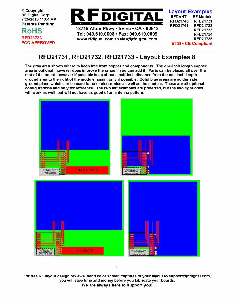
The gray area shows where to keep free from copper and components. The one-inch length copper area is optional, however does improve the range if you can add it. Parts can be placed all over the rest of the board, however if possible keep about a half-inch distance from the one inch length ground area to the right of the module, again, only if possible. Solid blue areas are solder side ground plane which can be used for user electronics as well as the module. These are all optional configurations and only for reference.
RFD21731, RFD21732, RFD21733 - Layout Examples 7
13715 Alton Pkwy • Irvine • CA • 92618 Tel: 949.610.0008 • Fax: 949.610.0009 www.rfdigital.com • [email protected]
For free RF layout design reviews, send color screen captures of your layout to [email protected], you will save time and money before you fabricate your boards.
We are always here to support you!
11
© Copyright, RF Digital Corp. 7/25/2010 11:04 AM Patents Pending
RoHS RFD21733 FCC APPROVED
Layout ExamplesRFDANT RF ModuleRFD21743 RFD21731RFD21741 RFD21732
RFD21733RFD21734RFD21735
ETSI • CE Compliant
The gray area shows where to keep free from copper and components. The one-inch length copper area is optional, however does improve the range if you can add it. Parts can be placed all over the rest of the board, however if possible keep about a half-inch distance from the one inch length ground area to the right of the module, again, only if possible. Solid blue areas are solder side ground plane which can be used for user electronics as well as the module. These are all optional configurations and only for reference. The two left examples are preferred, but the two right ones will work as well, but will not have as good of an antenna pattern.
RFD21731, RFD21732, RFD21733 - Layout Examples 8
13715 Alton Pkwy • Irvine • CA • 92618 Tel: 949.610.0008 • Fax: 949.610.0009 www.rfdigital.com • [email protected]
For free RF layout design reviews, send color screen captures of your layout to [email protected], you will save time and money before you fabricate your boards.
We are always here to support you!
12
© Copyright, RF Digital Corp. 7/25/2010 11:04 AM Patents Pending
RoHS RFD21733 FCC APPROVED
Layout ExamplesRFDANT RF ModuleRFD21743 RFD21731RFD21741 RFD21732
RFD21733RFD21734RFD21735
ETSI • CE Compliant
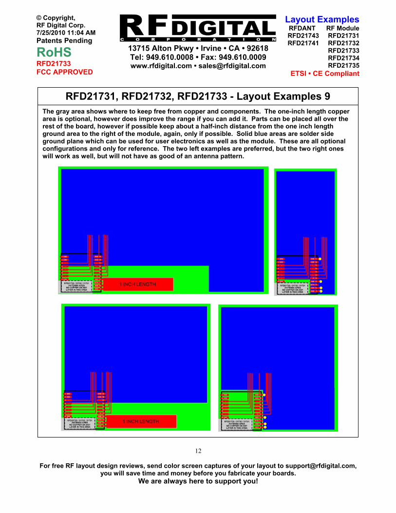
The gray area shows where to keep free from copper and components. The one-inch length copper area is optional, however does improve the range if you can add it. Parts can be placed all over the rest of the board, however if possible keep about a half-inch distance from the one inch length ground area to the right of the module, again, only if possible. Solid blue areas are solder side ground plane which can be used for user electronics as well as the module. These are all optional configurations and only for reference. The two left examples are preferred, but the two right ones will work as well, but will not have as good of an antenna pattern.
RFD21731, RFD21732, RFD21733 - Layout Examples 9
13715 Alton Pkwy • Irvine • CA • 92618 Tel: 949.610.0008 • Fax: 949.610.0009 www.rfdigital.com • [email protected]
For free RF layout design reviews, send color screen captures of your layout to [email protected], you will save time and money before you fabricate your boards.
We are always here to support you!
13
© Copyright, RF Digital Corp. 7/25/2010 11:04 AM Patents Pending
RoHS RFD21733 FCC APPROVED
Layout ExamplesRFDANT RF ModuleRFD21743 RFD21731RFD21741 RFD21732
RFD21733RFD21734RFD21735
ETSI • CE Compliant
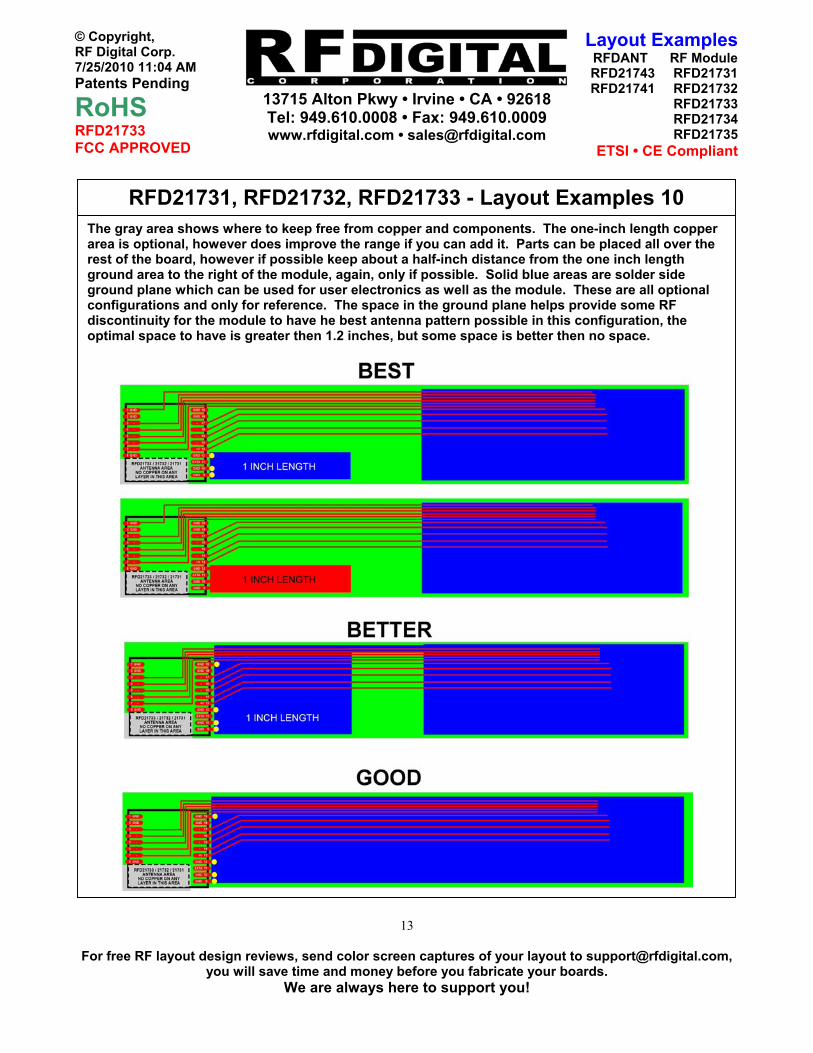
The gray area shows where to keep free from copper and components. The one-inch length copper area is optional, however does improve the range if you can add it. Parts can be placed all over the rest of the board, however if possible keep about a half-inch distance from the one inch length ground area to the right of the module, again, only if possible. Solid blue areas are solder side ground plane which can be used for user electronics as well as the module. These are all optional configurations and only for reference. The space in the ground plane helps provide some RF discontinuity for the module to have he best antenna pattern possible in this configuration, the optimal space to have is greater then 1.2 inches, but some space is better then no space.
RFD21731, RFD21732, RFD21733 - Layout Examples 10

13715 Alton Pkwy • Irvine • CA • 92618 Tel: 949.610.0008 • Fax: 949.610.0009 www.rfdigital.com • [email protected]
For free RF layout design reviews, send color screen captures of your layout to [email protected], you will save time and money before you fabricate your boards.
We are always here to support you!
14
© Copyright, RF Digital Corp. 7/25/2010 11:04 AM Patents Pending
RoHS RFD21733 FCC APPROVED
Layout ExamplesRFDANT RF ModuleRFD21743 RFD21731RFD21741 RFD21732
RFD21733RFD21734RFD21735
ETSI • CE Compliant
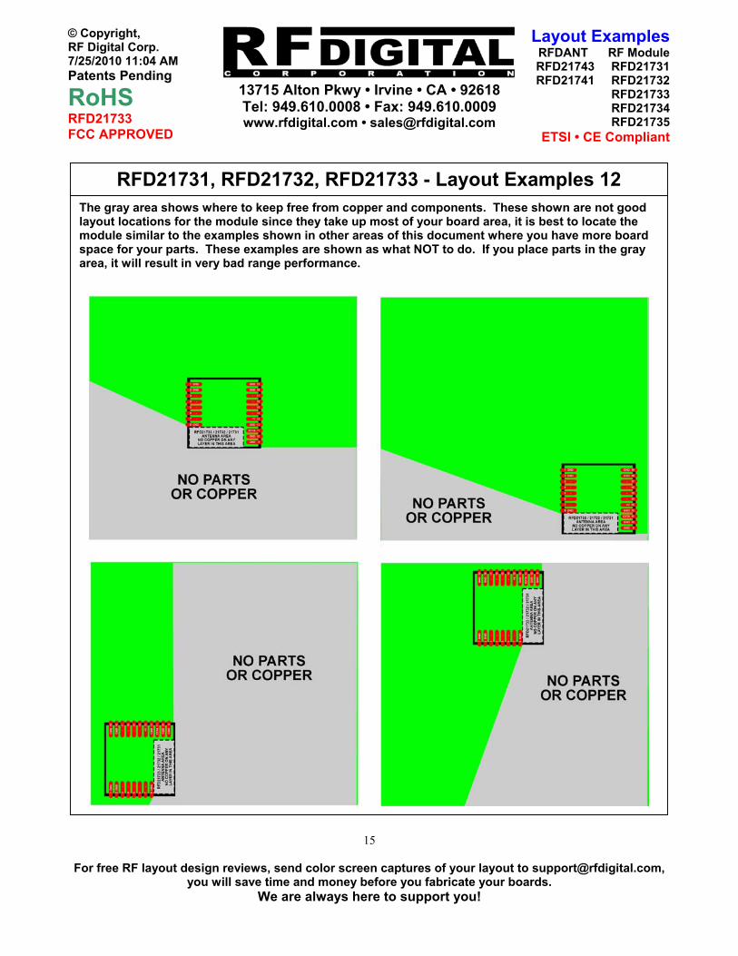
The gray area shows where to keep free from copper and components. These shown are not good layout locations for the module since they take up most of your board area, it is best to locate the module similar to the examples shown in other areas of this document where you have more board space for your parts. These examples are shown as what NOT to do. If you place parts in the gray area, it will result in very bad range performance.
RFD21731, RFD21732, RFD21733 - Layout Examples 11
13715 Alton Pkwy • Irvine • CA • 92618 Tel: 949.610.0008 • Fax: 949.610.0009 www.rfdigital.com • [email protected]
For free RF layout design reviews, send color screen captures of your layout to [email protected], you will save time and money before you fabricate your boards.
We are always here to support you!
15
© Copyright, RF Digital Corp. 7/25/2010 11:04 AM Patents Pending
RoHS RFD21733 FCC APPROVED
Layout ExamplesRFDANT RF ModuleRFD21743 RFD21731RFD21741 RFD21732
RFD21733RFD21734RFD21735
ETSI • CE Compliant
The gray area shows where to keep free from copper and components. These shown are not good layout locations for the module since they take up most of your board area, it is best to locate the module similar to the examples shown in other areas of this document where you have more board space for your parts. These examples are shown as what NOT to do. If you place parts in the gray area, it will result in very bad range performance.
RFD21731, RFD21732, RFD21733 - Layout Examples 12
13715 Alton Pkwy • Irvine • CA • 92618 Tel: 949.610.0008 • Fax: 949.610.0009 www.rfdigital.com • [email protected]
For free RF layout design reviews, send color screen captures of your layout to [email protected], you will save time and money before you fabricate your boards.
We are always here to support you!
16
© Copyright, RF Digital Corp. 7/25/2010 11:04 AM Patents Pending
RoHS RFD21733 FCC APPROVED
Layout ExamplesRFDANT RF ModuleRFD21743 RFD21731RFD21741 RFD21732
RFD21733RFD21734RFD21735
ETSI • CE Compliant
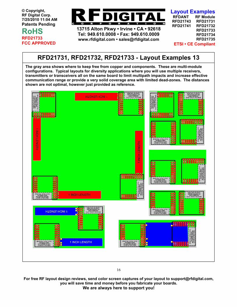
The gray area shows where to keep free from copper and components. These are multi-module configurations. Typical layouts for diversity applications where you will use multiple receivers, transmitters or transceivers all on the same board to limit multipath impacts and increase effective communication range or provide a very solid coverage area with limited dead-zones. The distances shown are not optimal, however just provided as reference.
RFD21731, RFD21732, RFD21733 - Layout Examples 13
13715 Alton Pkwy • Irvine • CA • 92618 Tel: 949.610.0008 • Fax: 949.610.0009 www.rfdigital.com • [email protected]
For free RF layout design reviews, send color screen captures of your layout to [email protected], you will save time and money before you fabricate your boards.
We are always here to support you!
17
© Copyright, RF Digital Corp. 7/25/2010 11:04 AM Patents Pending
RoHS RFD21733 FCC APPROVED
Layout ExamplesRFDANT RF ModuleRFD21743 RFD21731RFD21741 RFD21732
RFD21733RFD21734RFD21735
ETSI • CE Compliant
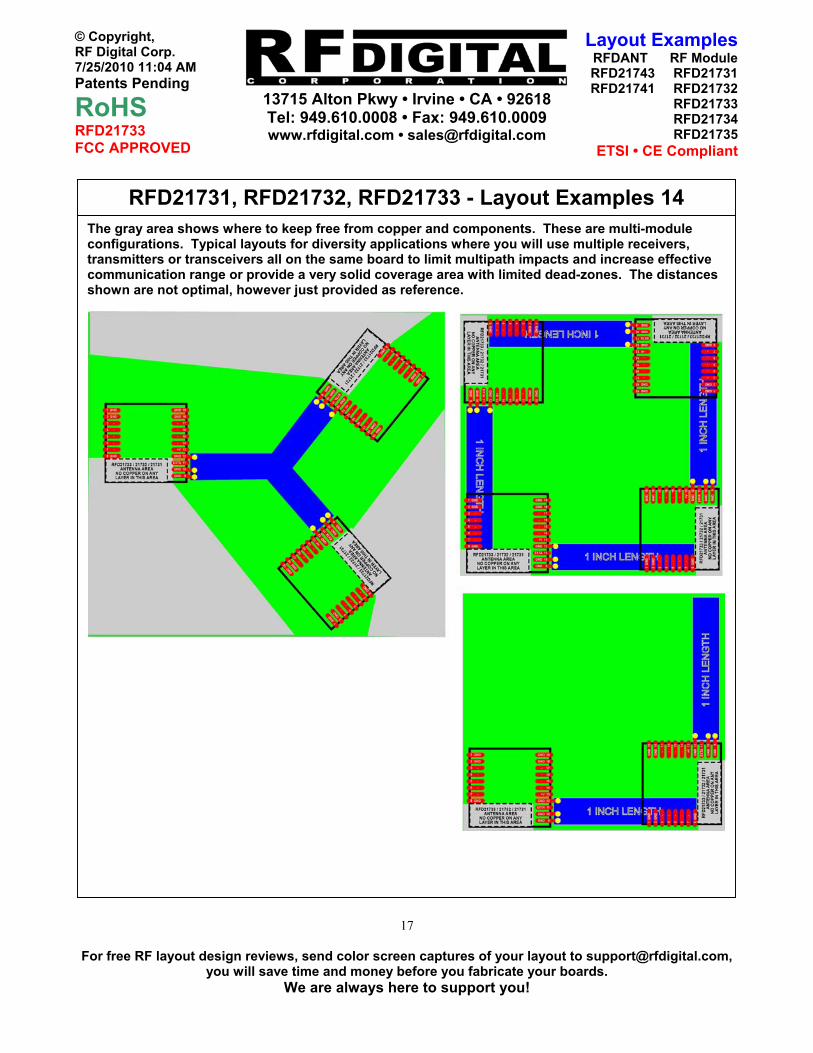
The gray area shows where to keep free from copper and components. These are multi-module configurations. Typical layouts for diversity applications where you will use multiple receivers, transmitters or transceivers all on the same board to limit multipath impacts and increase effective communication range or provide a very solid coverage area with limited dead-zones. The distances shown are not optimal, however just provided as reference.
RFD21731, RFD21732, RFD21733 - Layout Examples 14
13715 Alton Pkwy • Irvine • CA • 92618 Tel: 949.610.0008 • Fax: 949.610.0009 www.rfdigital.com • [email protected]
For free RF layout design reviews, send color screen captures of your layout to [email protected], you will save time and money before you fabricate your boards.
We are always here to support you!
18
© Copyright, RF Digital Corp. 7/25/2010 11:04 AM Patents Pending
RoHS RFD21733 FCC APPROVED
Layout ExamplesRFDANT RF ModuleRFD21743 RFD21731RFD21741 RFD21732
RFD21733RFD21734RFD21735
ETSI • CE Compliant
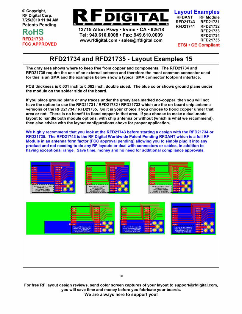
The gray area shows where to keep free from copper and components. The RFD21734 and RFD21735 require the use of an external antenna and therefore the most common connector used for this is an SMA and the examples below show a typical SMA connector footprint interface. PCB thickness is 0.031 inch to 0.062 inch, double sided. The blue color shows ground plane under the module on the solder side of the board. If you place ground plane or any traces under the greay area marked no-copper, then you will not have the option to use the RFD21731 / RFD21732 / RFD21733 which are the on-board chip antenna versions of the RFD21734 / RFD21735. So it is your choice if you choose to flood copper under that area or not. There is no benefit to flood copper in that area. If you choose to make a dual-mode layout to handle both module options, with chip antenna or without (which is what we recommend), then also advise with the layout configurations above for proper application. We highly recommend that you look at the RFD21743 before starting a design with the RFD21734 or RFD21735. The RFD21743 is the RF Digital Worldwide Patent Pending RFDANT which is a full RF Module in an antenna form factor (FCC approval pending) allowing you to simply plug it into any product and not needing to do any RF layouts or deal with connectors or cables, in addition to having exceptional range. Save time, money and no need for additional compliance approvals.
RFD21734 and RFD21735 - Layout Examples 15

13715 Alton Pkwy • Irvine • CA • 92618 Tel: 949.610.0008 • Fax: 949.610.0009 www.rfdigital.com • [email protected]
For free RF layout design reviews, send color screen captures of your layout to [email protected], you will save time and money before you fabricate your boards.
We are always here to support you!
19
© Copyright, RF Digital Corp. 7/25/2010 11:04 AM Patents Pending
RoHS RFD21733 FCC APPROVED
Layout ExamplesRFDANT RF ModuleRFD21743 RFD21731RFD21741 RFD21732
RFD21733RFD21734RFD21735
ETSI • CE Compliant
Important Notice RF Digital reserves the right to make corrections, modifications, and/or improvements to the product and/or its specifications at any time without notice. RF Digital assumes no liability for the user’s product and/or applications. RF Digital products are not authorized for use in safety-critical applications, including but not limited to life-support applications. RF Digital assumes no liability for parts or their application beyond replacement or refunding the original purchase price. All trademarks and trade names belong to their respective owners. End of Document.

Mouser Electronics
Authorized Distributor
Click to View Pricing, Inventory, Delivery & Lifecycle Information: RF Digital:
RFD21731 RFD21732 RFD21734