richtek advanced constant on time buck converters...
TRANSCRIPT
Richtek Advanced Constant On Time
Buck converters:
Richtek ACOTTM RT7275GQW EVM kit
Roland van Roy
FAE Richtek Europe
August 2014

Challenges with high load transient applications
Current Mode buck converter versus ACOT
ACOT design considerations
RT7275GQW EVM kit parameters
ACOT Frequently Asked Questions (FAQ)
ACOT design tools & application notes
Content

CONFIDENTIAL
Core
Challenges in powering High Transient Loads
Buck 0.8 ~ 1.2V
12V
Sudden processing 2A ~ 6A
FPGA, DSP and SoC applications can exhibit fast changing loads:
Output Voltage Sag under transient load should not affect normal operation
1A ~ 3A DDR Buck
1.5 ~ 2.5V Memory read/write
USB Buck 5V
Hot-plug events 0.5A ~ 2A
Dynamic load condition:
CONFIDENTIAL
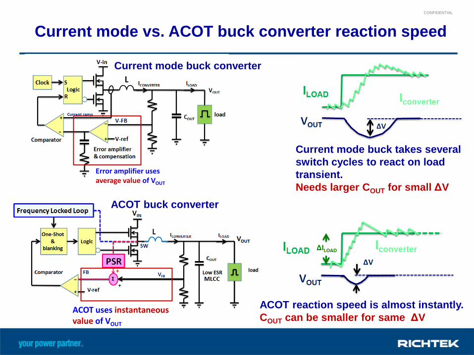
Current mode vs. ACOT buck converter reaction speed
ACOT reaction speed is almost instantly.
COUT can be smaller for same ΔV ACOT uses instantaneous value of VOUT
Error amplifier uses average value of VOUT
Current mode buck takes several
switch cycles to react on load
transient.
Needs larger COUT for small ΔV
ACOT buck converter
Current mode buck converter

CONFIDENTIAL
Design considerations for ACOT Buck converters
5
Add low ESR CIN for
input rail filtering and
check CIN RMS current
rating
EN for power
sequence or
connect to VIN for
auto-start.
Pgood for power
sequence or SoC
enable CSS sets
soft-start
time
Add some Cff for extra damping
(high VOUT and high COUT applications)
R1 & R2 set output
voltage
Select L-value
for 20 ~ 50%
current ripple
Select COUT for % sag
under load transient
or % output ripple

CONFIDENTIAL
RT7275GQW EVM KIT:
6
CIN for <30mVpp input ripple
CSS = 3.9nF:
Tss = 2.6msec
L1 = 1.4uH: Ripple = 1A (33% ripple)
COUT selected for
6.5mVpp output ripple
R1 & R2 set for 1.05V
output voltage
(Cff is not needed for
this 1.05V application)
EN pull-up to VIN:
Automatic start-up

CONFIDENTIAL
ACOT FAQ: Calculate and measure output ripple
7
Measurement setup:
Use short probe leads to minimize
inductor stray field noise pick-up
VOUTpp
VSW
Iinductor
EVM measurement result
How does output ripple happen?
In the RT7275GQW 1.05V evaluation board:
VRIPPLE measured: 6.8mVpp
Calculation method:
CONFIDENTIAL
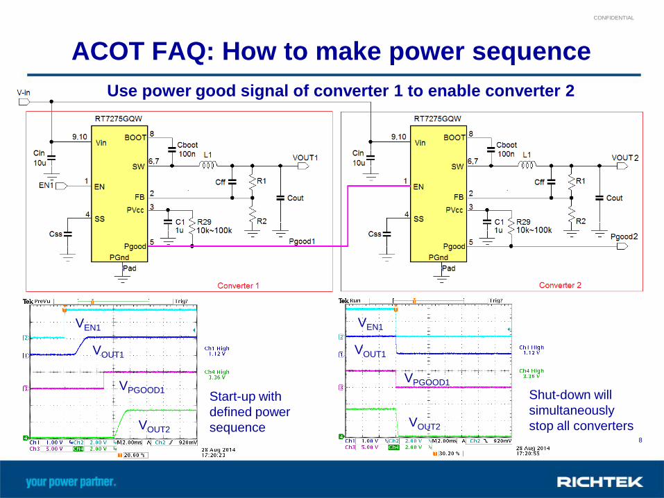
ACOT FAQ: How to make power sequence
8
Use power good signal of converter 1 to enable converter 2
Start-up with
defined power
sequence
VEN1
VOUT1
VPGOOD1
VOUT2
VEN1
VOUT1
VPGOOD1
VOUT2
Shut-down will
simultaneously
stop all converters

CONFIDENTIAL
ACOT FAQ: Calculate and measure output sag during load transient
9
Measurement method:
Apply a fast step load 1~2A/µsec at converter
output, using dynamic load or MOSFET switch
(or use a power resistor briefly touching the load)
Measurement setup:
(measured VSAG is lower
than calculated due to
rise time of load step)
VSAG
Measurement result:
In RT7275GQW 1.05V demo board and 2A fast load step:
Calculation method:
Output voltage sag
happens during load
transient rising edge

CONFIDENTIAL
ACOT FAQ: Calculate and measure output soar during load transient
10
In 1.05V demo board and 2A fast load step:
Output voltage soar
happens during load
transient falling edge
Calculation method:
The inductor current drops slower than load current,
thereby charging the output capacitor
Converter in 0% duty-cycle to
maximize output discharge
Measured VSOAR is lower
than calculated due to
fall time of load step
VSOAR
(soar pulse may have
different amplitude
depending on timing of
load step relative to the
last switching on-time)
Measurement result:
Measurement method:
Apply a fast step load 1~2A/µsec at converter
output, using dynamic load or MOSFET switch
(or use a power resistor briefly touching the load)

CONFIDENTIAL
ACOT FAQ: How to check converter stability
11
Step load measurement
showing under-damped
response (Cff needs to be
added or increased in value)
Relation between step load response
ringing, damping and phase margin
ACOT uses a non-linear constant ON time control system, and traditional open loop gain-
phase stability analysis methods are not suitable to be used with ACOT converters.
Closed loop analysis is valid for ACOT and can be used for mathematical calculations.
For practical stability measurements, it is recommended to use fast step loads to
measure the converter damping. Sufficiently damped response will not show any ringing,
and corresponds to a stable control loop.
Step load measurement
showing well-damped
response

CONFIDENTIAL
ACOT FAQ: How to tune Cff
12
The feed-forward capacitor plays a role in the
damping of the ACOT control loop, especially at high
duty-cycle applications like 12V 5V. For low duty-
cycle applications like 12V 1V it is normally not
needed. The value of Cff for a specific ACOT
converter depends on duty-cycle, COUT value,
inductor value and R1 value.
1. Apply a step load and if it shows
ringing, measure the ringing frequency
In this 12V 5V example: fRING=59.5kHz
2. Calculate Cff by the formula:
In this example: (R1 = 120k)
Practical method to find Cff value:
Without Cff
After adding Cff = 27pF: well-
damped step response
With Cff

CONFIDENTIAL
ACOT FAQ: ACOT converter with remote sense
13
Distance between converter and FPGA
Buck converter
FPGA load
Converter regulates VOUT local
Solution: Use remote sense
Feedback resistor
connection at
remote load side
Add RC snubber at load side to
damp the ringing that can happen
due to LPARASITIC and CLOAD
Use capacitor from VOUT local to
feedback to avoid instability due to
LPARASITIC & COUT phase delay (you can use OSCON capacitor as snubber)
ringing
Voltage droop
due to Rparasitic

CONFIDENTIAL
ACOT FAQ: Why do switch waveforms show frequency jitter?
14
ACOT uses a (pseudo) fixed TON, and controls TOFF to regulate the output voltage. This
means that load transients will always result in frequency changes in the switch waveform.
At steady load conditions, the duty-cycle will be constant, and the frequency locked loop will
slowly control TON for operation near the nominal frequency. However, there will always be
some frequency jitter visible in the switch waveform due to noise in the feedback signal.
At low VOUT applications, frequency jitter will be more than at high VOUT applications.
VOUT and switching waveform for a
12V 1.0V application
Switching waveform shows ~ 7% jitter
T-ON
SW
T-ON T-ON T-ON
PSR+VOUT
PSR+VOUT
VREF
SW
Noise band
Low VOUT
Low VOUT
SW
High VOUT
Noise band
High VOUT

ACOTTM Design tools & Application notes
CONFIDENTIAL
16
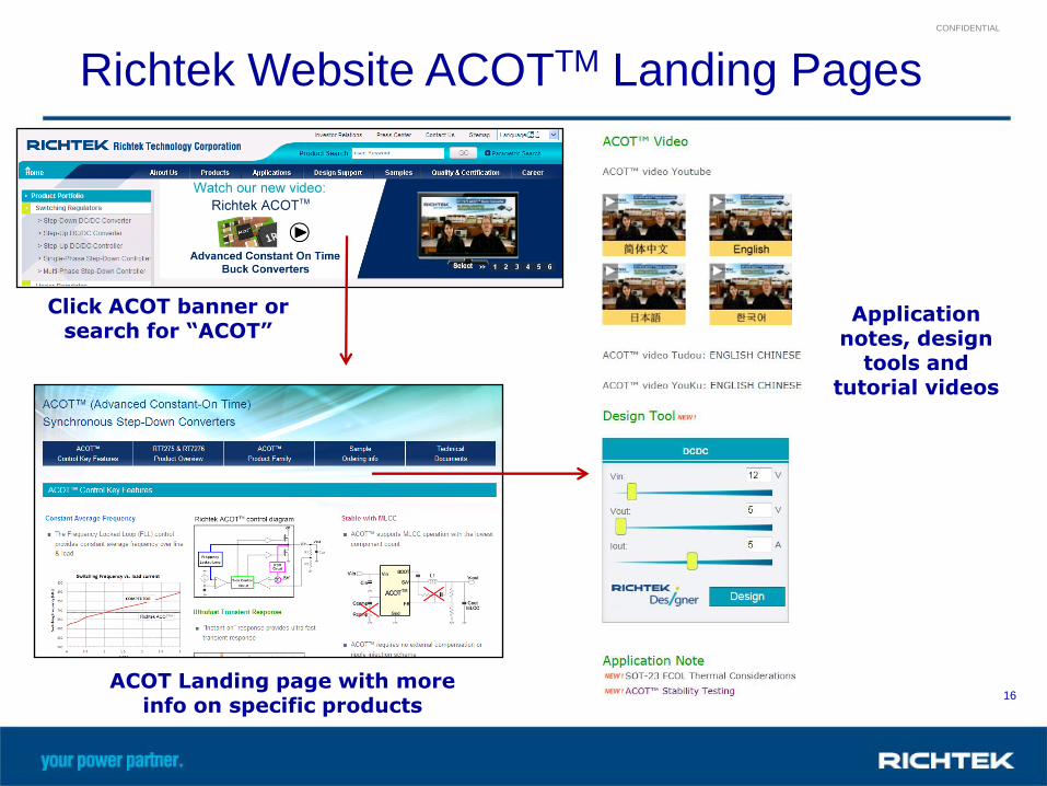
Richtek Website ACOTTM Landing Pages
ACOT Landing page with more info on specific products
Application notes, design
tools and tutorial videos
Click ACOT banner or search for “ACOT”

CONFIDENTIAL
17
Richtek Website Product Pages
Application notes and tools can be found under “Documents and Tools” tab
