rights / license: research collection in copyright - …25759/... · 4.3.3 piezo creep . . . . . ....
TRANSCRIPT

Research Collection
Doctoral Thesis
Scanning probe-based local spectroscopy of semiconductorheterostructures below 300mK
Author(s): Vančura, Tobias A.; Baltes, Henry
Publication Date: 2002
Permanent Link: https://doi.org/10.3929/ethz-a-004409593
Rights / License: In Copyright - Non-Commercial Use Permitted
This page was generated automatically upon download from the ETH Zurich Research Collection. For moreinformation please consult the Terms of use.
ETH Library

Diss. ETH No. 14705
SCANNING PROBE–BASED LOCAL
SPECTROSCOPY OF SEMICONDUCTOR
HETEROSTRUCTURES BELOW 300 mK
A dissertation submitted to theSWISS FEDERAL INSTITUTE OF TECHNOLOGY
ZÜRICH
for the degree ofDoctor of Natural Sciences
presented by
Dipl.Phys. Tobias A.Vancura
born on Dec 28, 1973 in Kaiserslautern (Germany)
accepted on the recommendation of
Prof.Dr. Klaus Ensslin, examinerProf.Dr. Henry Baltes, co-examiner
Dr. Thomas Ihn, co-examiner
June 2002

ii

TO MY PARENTS
ANTONÍN AND SILVIA
AND MY BROTHER
CYRIL
In the space of one hundred and seventy-six years the Mississippihas shortened itself two hundred and forty-two miles. Therefore [. . . ]in the Old Silurian Period the Mississippi River was upward of onemillion three hundred thousand miles long [. . . ] seven hundred andforty-two years from now the Mississippi will be only a mile andthree-quarters long. [. . . ] There is something fascinating about sci-ence. One gets such wholesome returns of conjecture out of such atrifling investment of fact.
— MARK TWAIN


Contents
Abstract xi
Riassunto xiii
Zusammenfassung xv
1 Introduction 1
2 Introduction to Scanning Probes 5
2.1 Scanning Probe Microscopy . . . . . . . . . . . . . . . . . . . 5
2.1.1 Forces in SPM . . . . . . . . . . . . . . . . . . . . . . 6
2.1.2 Contact Mode SPM . . . . . . . . . . . . . . . . . . . . 6
2.1.3 Dynamic Mode SPM . . . . . . . . . . . . . . . . . . . 6
2.1.4 Force Detection . . . . . . . . . . . . . . . . . . . . . . 7
2.2 Kelvin Probe . . . . . . . . . . . . . . . . . . . . . . . . . . . 8
2.2.1 Displacement Charge or Current . . . . . . . . . . . . . 9
2.2.2 Resonant Electrostatic Force . . . . . . . . . . . . . . . 10
2.3 Piezo-Electric Technology . . . . . . . . . . . . . . . . . . . . 11
2.3.1 Stick-Slip Mechanism . . . . . . . . . . . . . . . . . . 12
2.3.2 Implementation of Stick-Slip Motors . . . . . . . . . . 13
2.3.3 Tube Scanners . . . . . . . . . . . . . . . . . . . . . . 14
3 Introduction to 2DEGs and Nanostructures 17

vi CONTENTS
3.1 Two-Dimensional Electron Systems . . . . . . . . . . . . . . . 17
3.1.1 Realization of a Two-Dimensional Electron Gas . . . . . 17
3.1.2 Landau Quantization . . . . . . . . . . . . . . . . . . . 18
3.1.3 Quantized Hall Effect and SdH Oscillations . . . . . . . 19
4 Building a cryo-AFM for 300mK and 9T 23
4.1 Cryostat . . . . . . . . . . . . . . . . . . . . . . . . . . . . . . 23
4.1.1 Cryogenic Setup . . . . . . . . . . . . . . . . . . . . . 23
4.1.2 Vibration Isolation . . . . . . . . . . . . . . . . . . . . 26
4.2 Microscope Instrumentation . . . . . . . . . . . . . . . . . . . 27
4.2.1 z-Stage . . . . . . . . . . . . . . . . . . . . . . . . . . 28
4.2.2 xy-Stage . . . . . . . . . . . . . . . . . . . . . . . . . . 28
4.2.3 Scan Piezo and Tip . . . . . . . . . . . . . . . . . . . . 29
4.2.4 Positioning Sensor . . . . . . . . . . . . . . . . . . . . 31
4.2.5 Thermometry . . . . . . . . . . . . . . . . . . . . . . . 32
4.2.6 Cabling . . . . . . . . . . . . . . . . . . . . . . . . . . 33
4.2.7 Electronics . . . . . . . . . . . . . . . . . . . . . . . . 34
4.3 Operation Characteristics . . . . . . . . . . . . . . . . . . . . . 35
4.3.1 Scan Piezo . . . . . . . . . . . . . . . . . . . . . . . . 35
4.3.2 z-Stage and Positioning Sensor . . . . . . . . . . . . . . 36
4.3.3 Piezo Creep . . . . . . . . . . . . . . . . . . . . . . . . 37
4.3.4 Calibration of the xy-Stage . . . . . . . . . . . . . . . . 38
4.3.5 Low Temperature Calibration of Tuning Forks . . . . . 41
5 Tuning Forks and Phase Locked Loops 43
5.1 Tuning Forks . . . . . . . . . . . . . . . . . . . . . . . . . . . 43
5.1.1 Properties of Tuning Forks . . . . . . . . . . . . . . . . 44
5.1.2 A Model for a Tuning Fork . . . . . . . . . . . . . . . . 46
5.1.3 Admittance Model and Measurement . . . . . . . . . . 46

CONTENTS vii
5.1.4 Step Response at Resonance . . . . . . . . . . . . . . . 48
5.2 Phase Locked Loop . . . . . . . . . . . . . . . . . . . . . . . . 48
5.3 Noise in FM-Detection with a Phase Locked Loop . . . . . . . . 50
5.3.1 z-Feedback . . . . . . . . . . . . . . . . . . . . . . . . 51
5.3.2 Optimum Feedback Parameters . . . . . . . . . . . . . 52
5.3.3 Effect of Q and k on the Bandwidth . . . . . . . . . . . 53
5.4 Magnetic Fields . . . . . . . . . . . . . . . . . . . . . . . . . . 53
5.5 Advantages of Tuning Forks and PLLs . . . . . . . . . . . . . . 54
5.5.1 Drawbacks of Tuning Forks . . . . . . . . . . . . . . . 55
5.5.2 Advantages of Tuning Forks . . . . . . . . . . . . . . . 55
5.5.3 Comparison to Phase Control . . . . . . . . . . . . . . 56
6 Magnetic Barriers 57
6.1 Introduction . . . . . . . . . . . . . . . . . . . . . . . . . . . . 57
6.2 Hysteresis and Sensor Characterization . . . . . . . . . . . . . . 59
6.2.1 Sample . . . . . . . . . . . . . . . . . . . . . . . . . . 59
6.2.2 Magnetization Reversal in a Thin Cobalt Film . . . . . . 60
6.2.3 Sensor Characterization . . . . . . . . . . . . . . . . . 61
6.3 Better Samples: A Whole New World . . . . . . . . . . . . . . 62
6.3.1 Sample Geometry and Properties . . . . . . . . . . . . . 63
6.3.2 Measurements . . . . . . . . . . . . . . . . . . . . . . 64
6.3.3 Theoretical Model . . . . . . . . . . . . . . . . . . . . 66
6.3.4 Discussion . . . . . . . . . . . . . . . . . . . . . . . . 70
6.3.5 Final Remarks . . . . . . . . . . . . . . . . . . . . . . 71
7 Kelvin Probe and Scanning Gate Experiments 73
7.1 Kelvin Probe Measurements on 2DEGs . . . . . . . . . . . . . 73
7.1.1 Experimental Data . . . . . . . . . . . . . . . . . . . . 74
7.1.2 Distance Dependence of UCPD . . . . . . . . . . . . . . 76

viii CONTENTS
7.1.3 Electrostatics of a Tip above a 2DEG: General Consid-erations . . . . . . . . . . . . . . . . . . . . . . . . . . 76
7.1.4 Local Electron Density within the Plate Capacitor Model 79
7.1.5 Plate Capacitor with Donor Layer . . . . . . . . . . . . 81
7.1.6 Going Further . . . . . . . . . . . . . . . . . . . . . . . 83
7.2 Scanning Gate Measurements on 2DEGs . . . . . . . . . . . . . 84
7.2.1 Sample . . . . . . . . . . . . . . . . . . . . . . . . . . 84
7.2.2 Scanning Gate Setup . . . . . . . . . . . . . . . . . . . 85
7.2.3 Experimental Data . . . . . . . . . . . . . . . . . . . . 87
7.2.4 Analysis . . . . . . . . . . . . . . . . . . . . . . . . . 88
7.3 The Future . . . . . . . . . . . . . . . . . . . . . . . . . . . . . 91
A Samples 93
A.1 List of Samples . . . . . . . . . . . . . . . . . . . . . . . . . . 93
A.2 Process Parameters . . . . . . . . . . . . . . . . . . . . . . . . 93
A.2.1 Hall Bar . . . . . . . . . . . . . . . . . . . . . . . . . . 93
A.2.2 Ohmic Contacts . . . . . . . . . . . . . . . . . . . . . . 94
A.3 Sample Cleaning . . . . . . . . . . . . . . . . . . . . . . . . . 95
B Conductive Heat Load and Thermal Conductivities 97
Danksagung 113
Curriculum Vitae (deutsch) 115
Curriculum Vitae (english) 117

Constants and Formulae
Important physical constantsPlanck’s constant h 6.6261 ·10−34 JsElectron mass m0 9.108956·10−31 kgPermeability of vacuum ε0 8.8542 ·10−12As/VmImpedance of vacuum µ0 4π ·10−7
Quantum of resistance h/e2 25.812807kΩCharacteristics of 2DEGsFermi wave vector kF =
√2πns
Fermi velocity vF =
kFm∗
GaAs material properties at T = 4.2KLattice constant a 5.654 ÅBand gap Eg 1.52eVEffective mass m∗ 0.0665m0Bohr’s radius a∗B 100 ÅRydberg energy E∗
Ry 5.763meV
2D density of states
2D = m∗π
2 = 12πa∗B
2E∗Ry
2.816 ·1010
3D density of states
3D =
√
E/E∗Ry
2π2E∗Rya∗B
3 3.77 ·1015/meVcm3√
E/1meV
3D carrier density n3D 2.51 ·1015cm−3 · (EF/1meV)3/2
GaAs in magnetic fieldsLandau splitting EL = ωc 1.728meV ·B/1TCyclotron frequency ωc = eB/m∗ 2.635 ·1012 s−1 ·B/1TMagnetic length lc =
√
/eB 25.7nm/√
B/1TCyclotron radius ln = lc ·
√2n+1
Shubnikov–de Haas effect in GaAsFermi energy EF = e/m2∆(1/B) 1.728meV/∆(1T/B)2D density ns = 2e/h∆(1/B) 4.84 ·1010 cm−2 ·B/1T3D density n3D 0.532n3/2
s
Table 1: Important physical constants and formulae


Abstract
The goal of this thesis is twofold: (i) to realize a local experimental probe forsemiconductor nanostructures, and (ii) to develop experimental skills exploitingthe potential of scanning probe techniques for a more precise local investigationof mesoscopic devices and quantum Hall systems.
In particular, the two main approaches in nanotechnology, the scanning probemicroscopy and the semiconductor processing at nanoscale, shall be combinedwith low temperature magnetotransport techniques to study quantum devices.
The microscope built during this thesis is a scanning force microscope witha force detection based on tuning forks. The instrument operates below 300mKin a 3He-system. Magnetic fields up to 9T can be applied and a complete setupfor transport measurements is integrated.
A magnetic sensor is discussed and investigated with the focus on the pos-sibility to integrate it on a tuning fork for the use as probe for local magneticfields.
Kelvin probe measurements are performed on a two-dimensional electrongas implemented in AlGaAs. Together with a plate capacitor model the localelectron density can be extracted from the data. The result coincides within 10%with the data obtained from transport measurements. The limits of the modelare described and proposals for advanced models are given.
Scanning gate measurements on a patterned two-dimensional electron gasare shown. The results are the first steps towards a local investigation of subsur-face semiconductor nanostructures ranging from mesoscopic cavities, via quan-tum point contacts and quantum wires to quantum dots.


Riassunto
L’obiettivo di questa tesi è stato duplice: (i) si è realizzata una sonda per l’anal-isi locale delle nanostrutture di semiconduttore; (ii) si sono sviluppate abilità ecompetenze sperimentali, tali da sfruttare le potenzialità delle tecniche con son-da a scansione nello studio di dispositivi mesoscopici e sistemi ad effetto Hallquantistico.
In particolare, i due strumenti principali della nanotecnologia, la microscopiacon sonda a scansione e la lavorazione dei semiconduttori su scala nanomet-rica, sono stati combinati alle tecniche a bassa temperatura per lo studio deidispositivi quantistici.
Il microscopio realizzato durante il periodo del dottorato è un microscopio ascansione di forza, in cui la rilevazione della forza ‘e basata sull’uso di sottilibarrette di quarzo piezoelettrico tagliate a forma di diapason. Lo strumento rag-giunge temperature di funzionamento inferiori ai 300mK in un criostato ad 3He.Nel microscopio è integrato un apparato completo per le misure di trasporto edè inoltre possibile applicare campi magnetici fino a ±9T.
Viene descritto e studiato un sensore magnetico, con particolare attenzionealla possibilità di integrarlo su una tuning fork per ottenere una sonda magneticalocale.
Misure di sonda Kelvin sono effettuate su un gas elettronico bidimensionalein una matrice di AlGaAs. La densità elettronica locale può essere ricavata daidati sperimentali mediante un modello a capacitori a facce piane e parallele. Ilrisultato si accorda entro il 10% con il valore ottenuto dalle misure di trasporto.Vengono discussi i limiti del modello usato e proposti alcuni miglioramenti.
Misure con sonda scanning gate sono state eseguite su un gas elettronicobidimensionale strutturato. I risultati ottenuti sono un primo passo verso lo stu-dio locale delle nanostrutture di semiconduttore localizzate sotto una superficie,

xiv Riassunto
dalle cavità mesoscopiche, ai contatti quantistici di punto, ai fili quantici e aipunti quantici.

Zusammenfassung
Das Ziel dieser Arbeit liegt zweifach begründet: (i) eine lokale Sonde für Halb-leiternanostrukturen zu realisieren, und (ii) die für die genauere Untersuchungvon mesoskopischen und Quanten-Hall Systemen notwendigen experimentellenFähigkeiten zu entwickeln.
Im besonderen sollen die zwei Hauptansätze der Nanotechnologie, Raster-kraftmikroskopie und Strukturierung von Halbleitern auf Nanometerskala, mitMagnetotransportmessungen bei tiefen Temperaturen zur systematischen Un-tersuchung von Quantenphänomenen kombiniert werden.
Das Mikroskop, dass im Laufe dieser Arbeit gebaut wurde, ist ein Raster-kraftmikroskop mit einer auf Stimmgabeln basierenden Kraftdetektion. Das Ge-rät arbeitet bei Temperaturen unter 300mK in einem 3He-System. MagnetischeFelder von bis zu 9T können erzeugt werden und ein kompletter Aufbau, umTransportmessungen durchführen zu können, steht zur Verfügung.
Ein magnetischer Sensor wird beschrieben und mit dem Fokus untersucht,ihn auf einer Stimmgabel integriert als Sonde für lokale magnetische Messun-gen einzusetzten.
Kelvin–Sonden Messungen werden auf einem zweidimensionalen Elektro-nengas in AlGaAs durchgeführt. Zusammen mit einem Plattenkondensatormo-dell kann aus den Daten die lokale Elektronendichte gewonnen werden. DieResultate stimmen innerhalb von 10% mit den Daten aus Transportmessungenüberein. Daran im Anschluss werden die Grenzen des Models diskutiert undEmpfehlungen für Verbesserungen gegeben.
Zuletzt werden Scanning Gate Messungen auf einem strukturierten zwei-dimensionalen Elektronengas gezeigt. Die Resultate sind ein erster Schritt inRichtung einer lokalen Untersuchung von Halbleiternanostrukturen wie Quan-tenpunktkontakten, -drähten und -punkten.

xvi Zusammenfassung
Chapter 1
Introduction
Anyone on the air. . . ?
— SWANDIVE
About a hundred years ago quantum mechanics was developed. It proved tobe the theory of the 20th century in all fields of modern physics. Among the firstproblems solved by the new theory were the atomic energy spectra. Neverthe-less, testing quantum mechanics on the atomic scale could only be done in anindirect way. From this point of view, Binnig and Rohrer’s Nobel prize awardedinvention of the scanning tunneling microscope [12]∗ represents a milestone,particularly in condensed matter physics. For the first time, individual atomscould be seen in real space. The investigated structure at that time was a Si 7×7structure.
In scanning tunneling microscopy (STM) a conducting tip is scanned over aconducting sample. A bias voltage is applied between tip and sample and thetunneling current is measured. The distance between tip and sample is con-trolled by keeping the tunneling current at a defined set point.
The drawback of the tunneling microscopy lies in the nature of the method.Only conducting samples can be investigated.
Four years after the invention of the STM, Binnig, Quate and Gerber [11]presented the first atomic force microscope (AFM). Not the tunneling currentbetween tip and sample is used as the feedback parameter to keep the tip-sampleseparation constant, but rather the minute forces which act on the tip when itcomes into close proximity of the sample are monitored directly. At larger dis-
∗The bibliography is ordered alphabetically.

2 Introduction
tances, the main force is the attracting van-der-Waals force. Closer to the sam-ple the repulsive interaction of overlapping atomic or molecular wave functionstakes over.
Measuring these forces is non-trivial. In the first AFM by Binnig and Quate,a soft cantilever tip scanned the surface. The separation to the sample wascontrolled by monitoring the deflection of the cantilever with an STM sittingon top of the cantilever. The current flowing from the tip to the cantilever wasmeasured and used as the feedback parameter.
Today different methods are used. Usually a laser-beam is deflected by thecantilever and then detected with a photo diode. More involved setups use in-terferometric detection of the beam deflection. Another method that does notdepend on a laser, uses piezo-resistive cantilevers and the deflection is mon-itored electrically. The microscope presented here uses yet another detectionmethod based on oscillating tuning forks.
In solid state physics, a field of great interest over the last five decades hasbeen the evolving science of semiconductors. Molecular beam epitaxy allowsto grow semiconductor structures, where the layering of different kinds of ma-terials can be controlled on an atomic scale. This in turn made so–called two-dimensional electron gases — in particular two-dimensional electron gases atthe layer interface in a GaAs/AlGaAs heterostructure — possible. By engineer-ing the layers in such a way that the band structure of the materials allows fora thin energy well to build up at the interface between two layers, it becamepossible to trap electrons in a two-dimensional world. The wave function of theelectrons extends only in x- and y-direction, while it decays exponentially in thez-direction.
A very exciting piece of new physics in this field was the quantum Hall effectdiscovered in 1980 by v. Klitzing [85, 86]. Instead of rising monotonously withincreasing perpendicular magnetic field, the Hall resistance in a two-dimensionalelectron system shows distinct plateaus at integer multiples of h/ν ·e2. Not longafter, the fractional quantum Hall effect and the quantization of conductance inquantum point contacts were discovered.
By confining the electrons laterally, an even wider field opened with thepossibility to reduce the dimensionality further. The reduction in size finally ledto one-dimensional quantum wires and zero-dimensional quantum dots. This
3
border region between the macroscopic world and the microscopic environmentof the electrons is called mesoscopic physics.
Historically, all the experiments performed to investigate semiconductor het-erostructures were based on currents injected and voltages measured at macro-scopic contacts attached to the mesoscopic structures. Consequently only anaverage response of the complete system could be probed and all understand-ing of local properties relied mostly on macroscopic experimental evidence. Aprominent problem that could not yet be solved without local probes is the ques-tion, where exactly in the sample the currents flow in the quantum Hall regime.
Enters the aforementioned scanning force microscope. Suddenly it becomesfeasible to investigate sample properties on a microscopic scale. The only re-maining problem is that the microscopes usually operate at room temperaturewhereas the interesting effects in today’s heterostructures occur at low temper-atures, i. e., at least liquid at nitrogen, usually liquid Helium and sometimes atmilli-kelvin temperatures.
This is the motivation for this thesis: To build a scanning probe microscopethat is capable of operating in a range between room temperature to below300mK and to investigate the local properties of semiconductor heterostruc-tures.
The reason to go down to 300mK and not stop at a conventional 4He cryostatis that below 300mK, the phase coherence length of the electron comes into therange of the sample size, i. e., about one micron. Interesting experiments comeinto reach.
The instrument is a home built scanning probe microscope based on tuningfork cantilevers. The scanning tip is attached to one prong of the tuning fork andthe oscillation is detected electronically. Optical detection for our applicationis not suitable, because the photons would excite the electrons in the sampleand alter its electronic properties. The tip is contacted separately such thatcapacitance and scanning gate measurements are easily performed.
The frequency detection is done with a phase locked loop allowing for anaccuracy better than 1 : 107.
Additionally to the low temperatures, a magnetic field of up to ±9T perpen-dicular to the sample surface can be applied during a scan. Coaxial cables and aset of constantan and manganine wires permit accurate measurements of small

4 Introduction
signals in sample and probe. The hold time at temperatures below 300mK is upto five days despite the high number of cables in the system.
The system is reliable enough that it is possible to measure safely over weekswithout warming it over 4K or crashing the tip.
The experiments performed with the microscope were Kelvin probe mea-surements on an unpatterned AlGaAs heterostructure. Embedded in the struc-ture lies a 2-dimensional electron gas. With the help of a plate capacitor modelwe could extract the local charge carrier density of the sample. This data coin-cides within 10% with densities extracted from transport measurements.
On a patterned sample, scanning gate measurements were performed. To dothis, the resistance of the structure is recorded while the tip scans over the sur-face and interacts with the electrons in the underlying two-dimensional electrongas. The results are consistent with the Kelvin probe data measured earlier.

Chapter 2
Introduction to Scanning Probes
Far out in the uncharted backwaters of the unfashionable end of theWestern Spiral arm of the Galaxy lies a small unregarded yellow sun.Orbiting this at a distance of roughly ninety-eight million miles is anutterly insignificant little blue-green planet whose ape-descended lifeforms are so amazingly primitive that they still think digital watchesare a pretty neat idea. . .
— DOUGLAS ADAMS,“THE HITCHHIKER’S GUIDE TO THE GALAXY”
As mentioned in the introduction, the investigation of local properties of two-dimensional electron gases is the main interest of this thesis. The temperaturesat which the interesting effects occur, are usually below 4.2K and scanningforce microscopes (SFM) capable of working at these low temperatures are notcommercially available. Hence the construction of such a microscope in a 3He-system was one of the main topics of this thesis. This chapter will introduce acouple of aspects that are important for the microscope and the measurementsmade with it.
2.1 Scanning Probe Microscopy
After the invention of the scanning tunneling microscope (STM) by Binnig andRohrer [12] and later of the atomic force microscope (AFM) by Binnig, Quateand Gerber [11], a huge variety of different scanning probes was invented. Theyare all based on a similar set of basic principles.

6 Introduction to Scanning Probes
2.1.1 Forces in SPM
The forces that can be detected with scanning probe microscopy are manifold.Usually one measures a combination of several forces acting between the tipand the sample. Among the most important of these are
• attractive van-der-Waals forces,
• repulsive forces due to overlapping wave functions of the tip and the sam-ple,
• electrostatic forces,
• magnetic forces,
• dissipative forces, in particular frictional forces,
• and chemical forces (of particular interest for the study of chemical bonds).
2.1.2 Contact Mode SPM
Scanning tunneling microscopy is usually done in the static mode, i. e., the tipstays above the surface at a constant distance. A feedback controller tries tokeep the tunneling current between the tip and the conductive sample constantby regulating the z-position of the tip.
A similar mode exists for the atomic force microscope. The force on the tipis held constant again by regulating the tip-sample separation. This is done inthe repulsive regime, i. e., the cantilever is deflected due to the tip being in directcontact with the surface. The signal of the deflection is used for the feedback.
Contact mode AFM is not widely used anymore. The main disadvantageis the direct contact of the tip with the surface during the entire scan. As aconsequence the quality of tip degrades quickly and resolution decreases.
2.1.3 Dynamic Mode SPM
Instead of keeping the tip still one can actively excite a motion of the tip. Usu-ally this motion is perpendicular to the sample, i. e., in the z-direction. To excitethe motion, one usually operates cantilevers with a scanning tip fixed at the front

2.1 Scanning Probe Microscopy 7
part of the oscillator. Generally, the cantilevers are operated at their resonancefrequency. The tip moves up and down and probes its interaction potential withthe surface. Due to the force between the sample and the tip the resonance fre-quency of the cantilever is altered with respect to the frequency of the freelyoscillating cantilever. Of course the mechanical amplitude of the motion is in-fluenced as well.
Usually, the mechanical amplitude of the cantilever z-motion is much smallerthan the typical length scales of the tip-sample potential. Figure 4.17 showsa typical force-distance curve with first an attractive branch and closer to thesample surface the repulsive branch. The branches differ in the sign of dF/dz.
By choosing the set-point of the z-feedback, one can either operate the mi-croscope in the repulsive or in the attractive regime.
Tapping Mode Operating the microscope in the repulsive part of the force-distance curve is called tapping mode. Over a short period of time, the tipcomes close enough to the surface to feel the repulsive force and then bouncesof.
The tapping mode is very stable feedback mechanism and usually the pre-ferred mode for AFM operation.
Non-Contact mode When the set-point for the z-controller is chosen such thatthe tip-sample interactions are dominated by the attractive forces, the tip doesnot reach significantly into the repulsive part of the interaction potential. Thisis called non-contact mode. Only in this mode, true atomic resolution wasachieved. [25, 26]
The non-contact mode is rather difficult to handle because a sudden pertur-bation that brings the tip in the repulsive part will inevitably force the feedbackcontroller to bring the tip even closer to the sample and crash the tip.
2.1.4 Force Detection
The forces acting on the cantilever can be detected in at least three differentways.
8 Introduction to Scanning Probes
Amplitude Detection Either, one can monitor the amplitude of the oscillation.The cantilever oscillates slightly off resonance and the change in amplitude canbe translated in a change in the tip-sample separation.
Phase Detection The second alternative is phase detection. At the resonance,the phase between the signal driving the cantilever and the response changesfrom +90 to −90. The zero crossing of the phase is an ideal candidate for afeedback parameter.
Frequency Detection Finally, the most complicated mechanism is a frequencydetection. The cantilever is always excited at its momentary resonance fre-quency. In order to do this one has to track the resonance of the oscillator. Thedrive signal is then phase locked to the response of the oscillator. Our setupis realized in this way and the complete chapter 5 is devoted to phase lockedloops.
The input signal for the z-feedback is the frequency shift ∆ f between thecurrent frequency and the resonance frequency of the unperturbed oscillation.
A very broad overview of different techniques used in scanning probe mi-croscopy is given in the PhD thesis of Jörg Rychen [71]. For a detailed monog-raphy on scanning probes the reader is referred to [16, 75].
2.2 Kelvin Probe
In 1898, Lord Kelvin developed a method to measure the contact potential dif-ference (CPD) of a material in reference to a known standard [47]. The CPDis defined in terms of the difference of the chemical potentials µch of the twoneutral solids, UCPD =
µche . By an electrical connection the electro-chemical
potentials µelch tend to equilibrate, resulting in a build up of an electrostatic po-tential φ . The electro-chemical potential µelch is the sum of the chemical andthe electrostatic potential
µelch = µch + eφ .

2.2 Kelvin Probe 9
N.B. As the following discussion will involve a rather large set of differentfrequencies, we will adopt the convention that frequencies corresponding tolock-in measurements will be denoted with ω and frequencies that are relatedto the oscillation of a tuning fork cantilever (resonance frequency, frequencyshift) shall be named with the letter f .
So far, we only talked about potentials. Laboratory equipment though mea-sures voltages, i. e., the differences in electrical potentials. Therefore one has torewrite all expressions with potentials to only contain potential differences.
The charge Q on a capacitor is a function of its capacitance C. Usually onemeasures a current, which is given by
dQdt
= (U −UCPD)dCdt
, (2.1)
and hence periodical variations in C will cause a periodic charge or current. Thesignal (2.1) can be nulled by adjusting the external electro-chemical potentialdifference U such that the electrostatic potential difference U −UCPD vanishes.
The CPD is very sensitive to surface properties and treatment. It is generallya function of the position on the surface. The scanning dynamic force micro-scope is ideally suited for a local measurement of the CPD because the probeand therefore the capacitance are oscillating [60]. The tip-sample capacitance asa function of tip position is also of interest and can be measured simultaneously.
Experimentally, either the electric field is nulled by a feedback controlling ofthe tip-sample bias voltage which signals the local CPD [41], or the tip-samplevoltage is kept fixed and the variations of the electrostatic potential as a functionof tip position are recorded. The nulling of the electric field allows the scanningprobe to be electrically non-invasive and is of importance even if the CPD is notof interest at all. Several operation modes will be discussed in the following.
2.2.1 Displacement Charge or Current
The distance between tip and sample is modulated with a frequency ω ,
∆z(ω) = z0 sin(ωt) .
Then the ac-current I(t) flowing is given by
I(t) = Q(t) = (U −UCPD)ddz
· z0ω cos(ωt) .

10 Introduction to Scanning Probes
For the actual measurement of the UCPD, the external bias voltage U betweensample and probe is adjusted until the space between tip and sample is field freeand the current goes to zero [59, 77, 88]. Care has to be taken to discriminatethe capacitive coupling of the excitation signal for the oscillator via parasiticcapacitances to the tip. As a variant, the voltage induced on the tip can bemeasured with high impedance instead of the current measured with low inputimpedance.
2.2.2 Resonant Electrostatic Force
When using the above mentioned frequency detection, the signal important forthe AFM-feedback is the frequency shift ∆ f = fts − f0 between the resonancesof the freely oscillating cantilever and the cantilever interacting with the sample,i. e., when the tip is within the interaction range of the sample.
At low mechanical amplitudes, ∆ f is usually assumed to be proportional tothe gradient of the tip-surface interaction force Fts [3]:
∆ f ≈ f0
2kdFts
dz(2.2)
An electrostatic force Fts acting on the two parts of a capacitor is given by
Fts =dEdz
=12
dC(z)dz
· (U −UCPD)2 , (2.3)
where E is the electrostatic energy, U is an external voltage applied between tipand sample.
The index ts is chosen for the force, because the capacitor we are interestedin will be the tip-sample system.
By applying a small ac-voltage in addition to a dc-voltage U(t) = Udc +Uac cos(ωt), the force can be split into two components,
Fts ∝ Fω · cos(ωt)+F2ω · cos(2ωt) .
Resulting, one gets an ω-periodic force proportional to the electrostatic poten-tial difference,
Fω =dCdz
· (Udc −UCPD)Uac ,

2.3 Piezo-Electric Technology 11
and a force at twice the frequency, 2ω , which is determined by the derivative ofthe capacitance
F2ω =12
dCdz
U2ac .
The frequency ω is usually chosen to match either the resonance frequency ofthe cantilever or its half frequency in order to have the double frequency signalon the resonance.
Because the first resonance of the cantilever is usually used to perform thedistance regulation, one can imagine to use the second flexural mode of thecantilever for the Kelvin probe.
2.3 Piezo-Electric Technology
In a scanning probe microscope, coarse motion mechanisms are needed for vari-ous parts. One usually uses motors based on piezo-electric materials (“piezos”).This chapter describes how piezos work and how they can be used in scanningforce microscopy.
Stress applied to an ionic solid displaces the equilibrium ion positions. Theleft part of Fig.2.1 shows a unit cell of a crystal with a center of symmetry. Thecell remains symmetric upon compressive force. However the unit cell shownon the right side of Fig.2.1 lacks a symmetrical center and hence the positiveand negative ions are displaced from their centroids.
In a piezo-electric material this stress leads to a voltage building up betweenthe two ends of the element. Conversely, applying a voltage to two ends of apiezo leads to its deformation.
The piezo-electric materials used in scanning probes are usually a type oflead zirconate titanate (PZT) ceramics. Unlike the piezo-electric quartz singlecrystals of which tuning forks are made of, PZT can be moulded into the desiredshape with the molecular electric dipoles initially pointing in random directions.Orientation of the dipoles is achieved by applying a strong electric field in thedesired direction during the moulding process.
A disadvantage for low-temperature applications is the thermal dependenceof the piezo-electric coefficients. The mechanical response of a piezo to anapplied voltages drops significantly at low temperatures. Chapters 4.3.4 and

12 Introduction to Scanning Probes
4.3.1 show these effects.
The polarization of PZT can deteriorate over time due to relaxation of thedipoles. Conditions accelerating this effect can be temperatures exceeding theCurie temperature TC and electrical fields larger that the depolarization field Edof the piezo-electric material.
Figure 2.1: Ionic displace-ment under an applied stressin a non-piezo-electric material(left) and a piezo-electric mate-rial (right).
2.3.1 Stick-Slip Mechanism
In a scanning force microscope, a coarse motion mechanism is needed in twosituations. The first and most important is the movement of the scanning unitwith the tube scanner in the z-direction towards and away from the sample. Thesecond is the coarse positioning of the sample underneath the tip. With suchan xy-stage it is possible to move the sample in a position where the interestingregion lies underneath the tip.
Figure 2.2 shows the working principle of such a motor. Many coarse po-sitioners utilize a stick-slip mechanism relying on the breaking of the staticfriction between two flat hard smooth surfaces.
Figure 2.2: Mechanism of aslip-stick motor. The lighterbar slides over the fixed darkerpiezo. The red dot on the saw-tooth indicates to where in thevoltage cycle the image abovebelongs.
t
U
stick stick stick slip
During the stick-phase, the piezo drags the movable part along in one direc-tion. In the other direction, during the slip-phase, the lateral acceleration breaksthe stiction and the piezo returns to its original position while the movable part

2.3 Piezo-Electric Technology 13
stays in its new position. Continuous motion along one axis is achieved byrepeatedly applying the sawtooth to the piezo.
The friction between the two parts depends on the surface properties in-cluded in the friction coefficient µ and the normal force acting on the surfaces.
Ffric = µFN
The static friction between the piezos and the movable parts is bigger thanthe dynamic friction, ∆µ = µst − µdyn > 0. Therefore the decisive quantity isthe force breaking the static friction during the slip-phase.
F =dpdt
= mdvdt
(2.4)
The force depends on the shape of the peak, i. e., the acceleration, and on themass of the table. The heavier the table, the better it will perform.
2.3.2 Implementation of Stick-Slip Motors
Depending on the design of the motor, one can either use stacks of shear piezo,small piezo tubes with a 4-quadrant electrode on the outer diameter, or evenstacks of piezos polarized normal to the plate. We will only consider the formertwo possibilities.
When the design leaves enough space for piezo tubes instead of shear stacks,tubes are the alternative that is much simpler to handle.
The cabling for tubes is much simpler. The four electrodes on the outside aretrivial to contact. Only the inner electrode might be a concern because a smallhole has to be drilled into the tube to insert a cable.
Stacks on the other hand have to be contacted at each layer separately. Witha thickness of 0.5mm per stack and voltages of up to 500V this can be non-trivial because of electrical break-through between the plates. Especially whenthe stacks become higher and should provide motion in two directions, i. e., ina xy-setup, this becomes an inhibiting obstacle.
Meanwhile, commercial stacks are available from the company PI Ceram-ics/Polytec PI, Inc∗.
∗http://www.polytecpi.com/offices.htm

14 Introduction to Scanning Probes
z−electrodes
xy−electrodes
Figure 2.3: Scan piezo with 4-segment electrode. With the inner electrode the z-motion iscontrolled.
One can drive tubes in a unipolar setup, though applying positive and neg-ative voltage pulses to opposing electrodes generates a higher deflection. Theinner electrode is grounded. The disadvantage of applying bipolar pulses tothe tubes is that the drive electronics is more involved. For stacks, only onepolarization is needed.
Piezo motors are the premium choice for operating all kinds of moving partsin a low-temperature, high-vacuum environment. They provide a reliable meansto achieve motion at conditions ranging from room to cryogenic temperatures.Depending on how they are set up, they can function as motors for coarse mo-tion over distances of several millimeters down to exact positioning of mechan-ical parts on the nanometer scale.
2.3.3 Tube Scanners
Scanning probe microscopy demands for a very accurate mechanism to movethe probing tip in x- and y-direction over the sample surface. During a scan, evenfiner motion in z-direction is needed in order to compensate for topographicalfeatures and tilt of the sample.
The most often used device — because it is relatively easy to handle — isthe tube scanner. The probing tip is mounted on one end of the tube while theother end is fixed on the z-stage. A piezo tube is schown in Fig.2.3.
The tube is made out of piezo-electric material with four electrodes on the

2.3 Piezo-Electric Technology 15
outer diameter (OD) and one on the inner diameter. By applying voltages ofopposite signs to two opposing electrodes one can bend the tube. A voltageapplied between the inner electrode and all four outer electrodes makes the tubecontract and stretch.


Chapter 3
Introduction to Two-Dimensional ElectronGases and Nanostructures
I don’t like this solid state physics [. . . ]. One shouldn’t work withsemiconductors, that is a filthy mess; who knows whether they reallyexist.
WOLFGANG PAULI, 1931
This chapter restates the most important properties of the physics of semi-conductors in two dimensions. Details of the calculations going further thanwhat is shown here can for example be found in [6, 7, 54, 83].
3.1 Two-Dimensional Electron Systems
If not stated otherwise, all magnetic fields mentioned in the following are per-pendicular to the two-dimensional electron gas (2DEG). Coordinates in theplane of the 2DEG are denoted by x and y, the z-coordinate is perpendicularto the plane.
3.1.1 Realization of a Two-Dimensional Electron Gas
When electrons are confined in a potential such that the free motion in z-directionis prohibited, one speaks of a two-dimensional electron gas. One possibility outof many to realize such a system is at an interface between AlxGa1−xAs andGaAs.

18 Introduction to 2DEGs and Nanostructures
Using molecular beam epitaxy (MBE), Al-, As-, Ga- and Si-atoms are de-posited on a plain GaAs wafer in ultra-high vacuum. In this way, it is possibleto grow the structure layer by layer. As the band gap of AlxGa1−xAs varies be-tween 1.54eV and 2.36eV, depending on the concentration x of aluminum, it ispossible to grow a potential profile. The material can be artificially doped by re-placing either Ga- or As-atoms with Si-atoms. Today, usually modulation dop-ing is used, meaning that a buffer is grown between the 2DEG and the dopant.The charge carriers can move to the interface, whereas the doping atoms, whichessentially are defects, remain outside the 2DEG. Greater mobilities and thuslower scattering rates are achieved with this technique.
3.1.2 Landau Quantization
A magnetic field B perpendicular to the 2DEG leads to a quantization of the sofar free movement of the electrons in the xy-direction. In the classical picture theelectrons are forced to move in closed orbits with a cyclotron frequency ωc =eBm∗ , m∗ being the effective electron mass and e the electron charge. Consideredquantum mechanically, the energy eigenvalues of these 2D electrons are
ε`,n = ε` +(n+12) ωc ±
12
gµBB, (3.1)
where ` = 1,2,3, . . . is the subband index and n = 0,1,2 . . . the Landau index.The Bohr magneton is µB = e
2m∗ . At high magnetic fields, the spin degeneracy ofthe subbands is lifted as taken into account by the last term of the equation. Forsemiconductors with a negative g-factor, the spin-up niveau is the energeticallyfavored state. The cyclotron frequency ωc is the same as in the classical case.
The density of states (DOS) in a two-dimensional system at zero magneticfield is constant and equal to 2D(B = 0) = m∗/π 2. With a magnetic fieldB 6= 0 at T = 0, only energy levels allowed by Eq.3.1 can be occupied and theDOS condenses into a series of delta functions. The levels are called Landaulevels.
In the case of a real 2DEG, different scattering processes broaden the Landaulevels (see Fig.3.1). Therefore, in order to observe the Landau quantization, themean scattering time τ has to be smaller than the cyclotron round trip time andthe thermal energies must be lower than the magnetic quantization energy:
ωcτ > 1 and kBT < ωc .

3.1 Two-Dimensional Electron Systems 19
!
localizedstates
0
extended states
Energy
DOS at B=0
D(E)
Figure 3.1: Density of states in a 2DEG with and without an external magnetic field. Thespin splitting is 1
2 gµBB.
With 2D denoting the density of states, gv and gs being the valley and thespin degeneracy, respectively, the degeneracy per unit area of each Landau levelis
η = 2D(E) · ωc =gvgsm∗ωc
2π = gvgseBh
.
3.1.3 Quantized Hall Effect and Shubnikov–de Haas Oscillations
The number of electrons in a system is constant and independent of the magneticfield. Due to the proportionality of the level degeneracy to the magnetic field,the Fermi energy jumps with increasing field to a lower niveau, as soon as thelevel’s degeneracy is large enough to hold all electrons. The number of occupiedLandau levels is known as the (integer) filling factor ν
ν =
[
gvgsns
η
]
=
[
heB
ns
]
,
where ns is the sheet density of the electrons and η the aforementioned leveldegeneracy.
At even filling factors, the Fermi niveau jumps between two levels with dif-ferent Landau indices, i. e., n → n± 1. At odd filling factors, one has a transi-tion between two spin-split niveaus of the same Landau level. A filling factor

20 Introduction to 2DEGs and Nanostructures
0 2 4 6 8
B[T]
0
500
1000
1500
2000
ρ xx[Ω
]
0200040006000800010000
ρ xy[Ω
]
Figure 3.2: Quantum Hall effect and Shubnikov–de Haas oscillations measured in a GaAssample grown by W. Wegscheider. The data was taken at T=100mK in a dilution refrig-erator. Spin splitting sets in at about 1.8T. The highest plateau above B = 7T lies atρxy = 8606Ω = h
e2 /3 and thus belongs to a filling factor ν = 3. ns = 5.7 · 1015 m−2,µ = 124m2/Vs. The maxima in ρxx for the spin-down electrons are strongly suppressed.The sample is I3 used in [83].
of ν = 4 signifies that the lowest two Landau levels (n = 0,1) are completelyfilled. At a filling factor of ν = 5, the spin-up level with n = 2 is occupied.
Measuring the Hall resistivity ρxy in a 2DEG yields plateaus at integer fillingfactors. Figure 3.2 shows a measurement. The values at which the plateausoccur is given by
ρxy =B
ens=
Beν e
hB=
1ν· h
e2
This explains the values at which the plateaus occur, but not why the plateausthemselves occur. In a magnetic field, electrons can be localized at impuritiesif the cyclotron radius is larger than the mean distance between two impurities,i. e., at high magnetic fields. At B 6= 0 there is a least one non localized state andnumerical simulations show that this extended state is in the middle of a broad-ened Landau level. Only the extended states can carry a current and hence theresistance does not change when the Fermi energy EF lies within the localizedstates. Plateaus arise at non integral filling factors.
The density of states at the Fermi edge determines the electrical conductanceof the 2DES (two-dimensional electron system). As the density is higher inthe center of a Landau level than in-between two levels, the longitudinal resis-tance oscillates as a function of the applied magnetic field. This phenomenon is
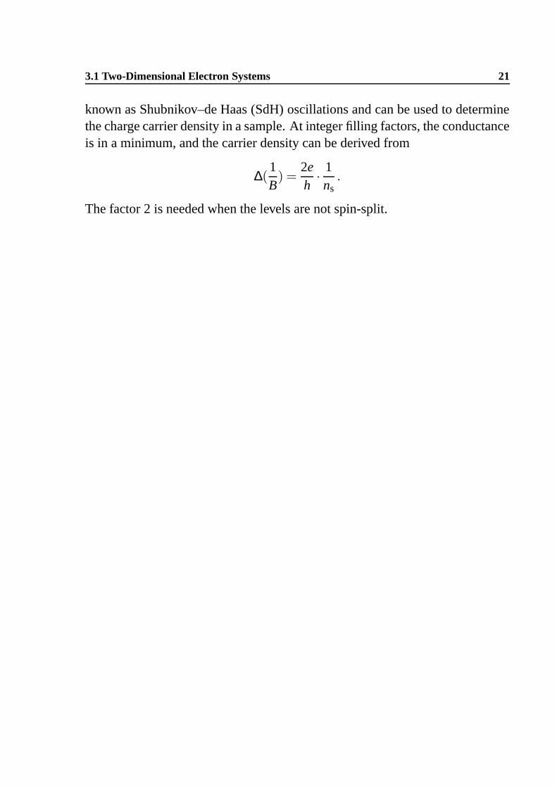
3.1 Two-Dimensional Electron Systems 21
known as Shubnikov–de Haas (SdH) oscillations and can be used to determinethe charge carrier density in a sample. At integer filling factors, the conductanceis in a minimum, and the carrier density can be derived from
∆(1B
) =2eh· 1
ns.
The factor 2 is needed when the levels are not spin-split.


Chapter 4
Building a cryo-AFM for 300mK and 9T
. . . and if you want to do this at low temperatures, you really have to bewilling to suffer.
— PAUL MCEUEN, EPS CMD Meeting 2002
This chapter describes the atomic force microscope developed and built forthis thesis. The design of the microscope tries to follow a modular strategywhich made it possible to build and test different parts independently. Thechapter will start with a description of the instrumentation and continue withresults of the characterization of the different modules.
4.1 Cryostat
The cryostat used in all the experiments is a single shot 3He-system from JanisInc. A rough outline of the inner vacuum chamber (IVC) is shown in Fig.4.1.A more complete sketch with the complete cryostat setup is given in Fig.4.4.
4.1.1 Cryogenic Setup
The main bath of the cryostat is isolated from room temperature by the outervacuum chamber (OVC), a liquid nitrogen jacket (LN2) and again a vacuumchamber. The 3He-insert resides inside the IVC. The whole IVC can be re-moved or inserted into the cryostat through a sliding seal at the top. The seal isconnected to the main bath only with a rubber boot to insure minimal mechani-cal contact.

24 Building a cryo-AFM for 300mK and 9T
Microscope
Vacuum Beaker
1K−Pot
Sorbtion Pump
3He−Pot
Figure 4.1: The inner vacuum cham-ber with 3He-system and thermome-ters and heaters.
The 1K-pot used to precool thesystem and condense the 3He is op-erated as a conventional 4He cryo-stat. The temperatures reached at thisstage are between 1.5 and 2K. Furthercooling of the 3He-pot is achieved bypumping on the condensed 3He.
At room temperature, the 3He re-sides in a dump outside the cryostat.When cooled, it gets adsorbed insidethe sorbtion pump. For the conden-sation into the 3He-pot, the sorbtionpump is heated and the 3He is releasedinto the 1K-Pot. There, it condensesagain into the 3He-pot. For our sys-tem, heating the sorbtion pump for 11
2hours suffices if the 1K-pot is cooledbelow 2K.
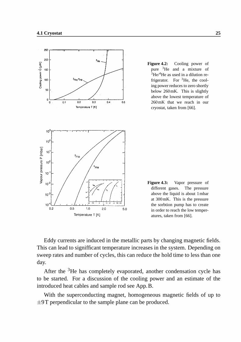
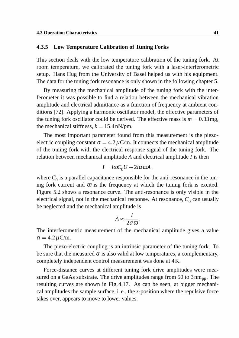
After completely condensing the3He, cooling the sorbtion pump re-duces the vapor pressure above theliquid 3He which starts to evaporate.This in turn leads to further cooling of the 3He-pot and the temperature will fallbelow 300mK within 20 to 30 minutes. In Fig.4.2 the cooling power of 3He isplotted vs. temperature. Figure 4.3 shows the vapor pressure of 3He.
The microscope is mounted on the bottom of the 3He-pot. This ensuresgood thermal coupling to the cryostat. Sample temperatures of 270mK can bereached routinely.
The hold time at a temperature below 300mK is more about three days ifthe 1K-pot is not cooled and stays at about 4K. Cooling the 1K-pot increasesthe hold time to up to five days and temperatures well below 270mK, usu-ally around 260mK. The helium consumption is about 6− 7l per day. Whilecondensing the 3He and during the cooldown from room temperature the con-sumption can be up to two times this value.
4.1 Cryostat 25
Figure 4.2: Cooling power ofpure 3He and a mixture of3He/4He as used in a dilution re-frigerator. For 3He, the cool-ing power reduces to zero shortlybelow 260mK. This is slightlyabove the lowest temperature of260mK that we reach in ourcryostat, taken from [66].
Figure 4.3: Vapor pressure ofdifferent gases. The pressureabove the liquid is about 1mbarat 300mK. This is the pressurethe sorbtion pump has to createin order to reach the low temper-atures, taken from [66].
Eddy currents are induced in the metallic parts by changing magnetic fields.This can lead to signifficant temperature increases in the system. Depending onsweep rates and number of cycles, this can reduce the hold time to less than oneday.
After the 3He has completely evaporated, another condensation cycle hasto be started. For a discussion of the cooling power and an estimate of theintroduced heat cables and sample rod see App.B.
With the superconducting magnet, homogeneous magnetic fields of up to±9T perpendicular to the sample plane can be produced.

26 Building a cryo-AFM for 300mK and 9T
4.1.2 Vibration Isolation
The room in which the experiment is set up is on the lowest floor of the buildingand vibrationally isolated. The cryostat sits inside a 2m deep pit.
Figure 4.4: The cryostat stands on its own support on the lowest floor of the building.The 3He-insert is vibrationally decoupled from the cooling system. The tubes holdingthe insert are filled with sand for lowering their resonance frequency.
Measurements of the vibration amplitudes and frequencies at various posi-tions in the lab and on top of the cryostat suggest that it is most favorable tocompletely decouple the microscope from the cryostat. Figure 4.4 shows howthis is achieved.
An annular plate of steel is mounted on a set of four heavy tubes that areanchored in the walls of the pit. The plate weighs about 30kg. The tubesare filled with sand in order to reduce their resonance frequency and damp the

4.2 Microscope Instrumentation 27
oscillation.
Another ring of steel is fixed on top of the support plate with four joints.The 3He-insert is lowered into the microscope through a sliding seal fixed tothe ring. This way, a rubber boot connecting the insert and the cryostat is theonly mechanical link between the main bath and the microscope.
The mechanical insulation is good enough such that it is possible to refillthe LN2 chamber while a scan is in progress. No signs of additional noise arevisible in the frequency signal.
In order to reduce the acoustic resonances of the cryostat, it is tightly wrappedinto a caoutchouc carpet.
4.2 Microscope Instrumentation
The microscope is mounted to the lower part of the 3He-pot. Two concentricrings of connectors fix the xy-stage on the inside and the microscope casing onthe outside to a ring screwed onto the 3He-pot. The xy-stage can be moved withthe help of a piezo motor. The sample-holder is mounted upside-down on thexy-stage. The z-stage can move up and down within the microscope casing. Thescan piezo with the scanning tip oriented towards the sample is fixed inside thez-module. A more detailed description of the setup is given on the followingpages.
The tip is glued onto one arm of a tuning fork. The tuning fork makes thetip oscillate above the surface. When the tip is lowered towards the surface, theresonance frequency changes due to the forces acting between tip and surface.This change in frequency is used as the error signal for the z-feedback.
A force-distance curve showing the attractive regime at long distances be-tween tip and sample and the repulsive regime at close proximity is shown inFig.4.17.
The detection of the shift of the resonance frequency is done with a phaselocked loop (PLL). The PLL is treated in Chap.5.2.

28 Building a cryo-AFM for 300mK and 9T
4.2.1 z-Stage
The purpose of the z-stage is coarse motion of the tip towards and away fromthe sample. We use a piezo motor as described in Sec.2.3.1 to accomplish this.
Figure 4.5: Sketch ofAFM-head. All lengthmeasures are in milli-meters.
The main ideas of the implementation comefrom the low-temperature UHV tunneling mi-croscope of the group of R.Wiesendanger de-scribed in [4, 63, 87] and the setup from Basel[34].
The stage is made as a triangular macorprism carrying the scan piezo. The modulesits inside the open cylinder that makes out thelower part of the z-module of the microscope(see Fig.4.6 left). From three sides, pairs ofshear piezo stacks clamp the stage. Two pairsare fixed to the casing and a third pair is pressedonto the stage with a copper-berylium (CuBe)spring.
Each stack is home-built and consists of fourpiezo plates. The plates are 0.5mm thick andare separately connected to the high voltage ca-bles. The gliding surfaces are sapphire plates ona aluminum-nitride support (see Fig.4.6 right).
The tuning fork with the scanning tip is at-tached to a support on the lower part of the scanpiezo such that it points towards the sample.
4.2.2 xy-Stage
Due to the different thermal expansion of the various parts of the microscope,the relative position of the tip above the sample changes during cooldown. Inorder to compensate for this, a motor had to be introduced to move the sampleat low temperatures. Again, this motor relies on piezos. Figure 4.7 shows aphotography of the xy-stage.

4.2 Microscope Instrumentation 29
Figure 4.6: Left: z-module. Right: Cut A−A as indicated in Fig.4.5.
The central plug mentioned above serves as the sample stage. Here, insteadof three times four stacks on each side of the supporting plug, piezo tubes areused. Connecting eight plates at a time proved too difficult and the new idea wasimplemented. Three small piezo tubes (diameter 3.175mm, length 18.0mm)pierce the plug. Six sapphire balls are glued on the top and bottom of eachtube. Two CuBe tables clamp the tubes with a spring. In order to reduce wear,the sapphire balls on the tubes run on sapphire plates inlayed into the tables.In the first design, plain copper-berylium was used instead of the inlayed sap-phire, and the sapphire balls left traces in the metal, finally inhibiting a reliableperformance.
On the side facing the z-stage, a chip socket is mounted onto the plate.
The stick-slip mechanism from Sec.2.3.1 is used to move the table. Becausethe tubes can bend in two orthogonal directions independently, the stage canmove in x- and y-direction.
A heater coil and two resistors for thermometry, one Pt100 and one Allen-Bradley (AB) resistor, are integrated into the stage to measure and regulate thesample temperature.
4.2.3 Scan Piezo and Tip
The scan piezo inside the z-stage is a simple tube scanner. The diameter is0.5in = 12.7mm and it is 2 in = 50.8mm long.
As our microscope is a dynamic force microscope, we need an oscillating

30 Building a cryo-AFM for 300mK and 9T
Figure 4.7: Photo of xy-stage. On the third image, the stage is oriented as it will be in themicroscope, i. e., with the sample holder pointing towards the bottom. This prevents dustfrom falling onto the sample.
cantilever. For reasons that will be explained in Chap.5, our oscillators areregular tuning forks as found in watches as a frequency standard. The tuningfork is oriented such that the plane in which it oscillates is oriented orthogonalthe sample plane. A conducting PtIr tip is glued by hand to the prong of thetuning fork close to the sample. After attaching the wire to the tuning fork,it is electro-chemically etched to form a sharp tip. The tip radius is typicallywell below 1 µm, 100nm are feasible as can be seen from the scanning electronmicroscopy (SEM) images shown in Fig.4.8.
The tip can be contacted separately via one of the semi-rigid thermo coaxcables.
Figure 4.8: SEM micrograph of a tip. Left: etched wire glued to tuning fork. Right:Close-up of tip. The tip radius is below 100nm.

4.2 Microscope Instrumentation 31
4.2.4 Positioning Sensor
A differential capacitive sensor is used to accurately detect the motion of thez-stage.
+90
−90
IUCl2l1
d
Figure 4.9: Capacitive position-ing sensor. The double electrodemoves with respect to the sin-gle electrode. The correspond-ing circuit is shown on the rightside.
As sketched in Fig.4.9, a split capacitor plate evaporated onto the movingz-stage is placed in opposition to a plate on the fixed part of the microscope.Two sine waves at frequency ω shifted by ±90 are applied to the two partsof the moving plate and the current flowing from the third plate is measured.When the two split plates and the fixed plate are arranged symmetrically, thecapacity of the broken plates with respect to the single plate is equal and no netcurrent flows to the IV-converter. As soon as the arrangement is detuned, thecapacitances of the two capacitors change and a current flows through the thirdport
I = Uex ω · wd
(l1 − l2) .
A1,2 = w · l1,2 is the effective area over which the two capacitor plates overlap,
w is the width of the plates. The change in position is ∆z = 12 · (l1 − l2).
Taking typical values d = 1mm, w = 1cm and applying a voltage U =6Vpp = 2.12Vrms at ω = 2π ·11kHz, one calculates
I∆z
= 7.5nAnm
.
Converting the current to a voltage with a factor of 106 V/A, i. e., using ancurrent to voltage converter (IUC) with a feedback resistor of 1MΩ, one canestimate a sensitivity of
∆z∆U
= 40nm/µV . (4.1)
The method is purely geometrical and it is therefore completely decoupledfrom thermal or pressure related effects.
The results of the calibration is discussed in Chap.4.3.2.

32 Building a cryo-AFM for 300mK and 9T
4.2.5 Thermometry
The first set of thermometers and heaters sits on the sorbtion pump. The heateris needed to warm up the pump during the condensation of the 3He. The ther-mometer is an Allen-Bradley carbon resistor.
Another Allen-Bradley resistor sits on the 1K-Pot. A calibrated RO600 re-sistor is located together with a heater coil on top of the 3He-pot. Two ther-mometers, one Pt100 for high temperatures and a carbon resistor for low tem-peratures, are directly integrated into the xy-table. A coil in the sample socketcan be used to heat the sample, e. g., during cool-down.
Finally there is one carbon resistor directly situated at the magnet. It shouldusually be at 4.2K when the cryostat is filled with helium.
The formulae describing the temperature dependence of the resistors are
TRO600 =1
A+B ·R2 ln(R)+C ·R3 (4.2)
TAB =B
ln(R)+C/ ln(R)−A. (4.3)
The parameter A,B and C are different for every resistor. They can be foundby fitting the above equations to the resistances at room, LN2 and LHe temper-atures. Alternatively, a calibration table can be used if available.
The heater resistances are given in Tab.4.1.
heater resistance
sorbtion pump 25Ω3He-pot 70Ωsample 45Ω
Table 4.1: Heater resistances at room temperature.
The resistances of the thermometers are measured with a 10-way multiplexedmultimeter from Agilent Technologies (34970A). The heaters are driven byYokogawa DC sources (7651). In principle it is possible to drive them with theabove 34970A and a current amplifier, but this has not yet been implemented.

4.2 Microscope Instrumentation 33
4.2.6 Cabling
A wealth of cables are needed for measuring the sample, operating the tuningfork, running the piezo-motors and the scan piezo, reading the z-position sensor,and finally for thermometry.
Introducing cables into the system always means an additional heat loadwhich reduces the hold time of the cryostat. Therefore all cables are ther-mally anchored at 4.2K, 1.5K and 300mK. Thermal anchoring is achievedby thoroughly winding the wires around copper posts attached to the varioustemperature stages.
For the high-voltage cables a different approach had to be taken. As shown inFig.4.10, very thin circuit boards with parallel leads of 10cm length were gluedto a thermal anchor. The wires are soldered to the two ends of the leads. Toprevent electrical breakthrough, the contacts are painted with polyimid varnish.∗
In order to further reduce the heat load on the low-temperature parts, specialcable materials with a low thermal conductance were used.
For the transport measurements, the cables used are made of constantan. Therelatively high electrical resistance of the material is not critical because onlysmall currents are run through the sample and resistances are usually measuredin a 4-terminal setup. The wires are braided into a 5mm wide ribbon for easierhandling.†
The resistors used for thermometry are connected with a similar set of ther-mally anchored constantan wires. The Pt100 and AB-resistor at the sample aremeasured in a 3-terminal setup to reduce the number of cables and connectorpins.
A set of six semi-rigid thermo-coax cables‡ is led to the 300mK stage andcan be used for small signals. Usually this includes the tuning fork drive volt-age and current, the connection to the tip and the z-position sensor. The drivevoltage for the z-position sensor is connected using constantan wires.
The piezo drives need special considerations. High resistance cables in con-junction with the piezo capacity act as low-pass filters cutting off the peaks
∗Tränklack 2053, available from Schweizerische Isola-Werke, CH-4226 Breitenbach.†available from Oxford Instruments.‡available from Thermo-Control GmbH, Riedstr.14, CH-8953 Dietikon.

34 Building a cryo-AFM for 300mK and 9T
driving the stage. On the other hand, low-resistance cables carry a high heatload which is not desirable either.
A compromise was found with home-built teflon-insulated manganine wiresused for both the drive voltages of the coarse steppers and the scan piezo. Thediameter of the cables used for the slick-stip motor is 3 times bigger than thehv-wires used for the scan piezo to reduce the resistance. With thinner wiresthe motor would not work. Table 4.2 shows the details on the cabling. Moreinformation on the cable induced heat loads can be found in App.B. There, anestimate for the heat introduced into the system is given for the different sets ofcables.
hv−cables
shielding
hv−cables
xy−table
heater
thermal anchor
He−pot3
Figure 4.10: Photo of the high-voltage thermal anchor at the 3He-pot. Left: Circuit boardwith wires soldered to leads. Right: Electrical shielding with adhesive copper tape.
4.2.7 Electronics
The AFM electronics is based on a TOPS3 system from Oxford Instruments.The high voltage amplifiers have been replaced and are now two separate boards

4.3 Operation Characteristics 35
cable material number diameter [mm] resistance [Ω]
scan piezo manganine 5 0.10 120z-motor manganine 2 0.30 13.6xy-motor manganine 5 0.30 13.6sample constantan 12 0.12 130coaxial steel 6 0.5 130
Table 4.2: Some parameters of the cables. The cables used for thermometry are the sameas the sample cables.
for the xy-stage and the z-motor respectively. The PI controllers for the PLL arehome-built.
4.3 Operation Characteristics
4.3.1 Scan Piezo
At room temperature the lateral scan range of the tube used is approximately50 µm reducing to roughly 8.8 µm at 4K. The tip can be extended ±2.5 µm inz-direction from the rest position at room temperature. At low temperatures thisreduces to ±425nm.
The scan range of the piezo was calibrated with scans on a 10 µm periodcalibration grid at room temperature and 4K. Figure 4.11 shows a scan on thegrid at room temperature.
The same sample can as well be used to calibrate the z-motion of the piezo.
Figure 4.11: Room temperaturescan on a calibration grid with aperiod of 10 µm.

36 Building a cryo-AFM for 300mK and 9T
Knowing the exact depth of the dips from a measurement with the calibratedDigital Instruments Nanoscope room temperature AFM, the maximum z-deflectionof the scan piezo can easily be calculated. Table Tab.4.3 shows the results.
T maximum scan range z-deflection
273K 7830 µm 33nm/V = 2530nm/75V4K 8.8 µm 5.6nm/V = 425nm/75V
Table 4.3: Maximum scan range and z-deflection of the scan piezo at room and liquidhelium temperature. The data was extracted from the scans on the calibration grid.
4.3.2 z-Stage and Positioning Sensor
In order to calibrate the z-motor, the tip was brought close enough to the sample,such that the tip could reach the surface. The position where the tip hit thesurface was recorded before the stage was moved again. The left-hand part ofFig.4.12 shows the corresponding plot. On the right hand of the same figure,the signal from the IU-converter connected to the capacitive position sensor isplotted against the position of the stage.
0 10 20 30 40position [steps]
-2000
-1000
0
1000
z [n
m]
-250 -200 -150 -100 -50 0position [steps]
-2.5
-2
-1.5
-1
-0.5
0
U [m
V]
Figure 4.12: Room temperature calibration of coarse z-motor. Left: Extension of tip untilsample is reached vs. motor steps. Right: Voltage read from capacitive sensor plotted vs.motor steps. The signal was measured at 11kHz and an excitation voltage of 6.0Vpp.
The slopes are 8.61± 0.7 µV/step and −89.6± 1.8nm/step respectively.One can thus calculate a sensitivity of 10.4nm/µV. This is even better than theestimated value of 40nm/µV from Eq.4.1.
The rising edge of the wave form used to drive the piezo motor is propor-tional to x4. This proved to be a good wave form for the stick-slip operation.

4.3 Operation Characteristics 37
-2 0 2 4 6 8t [ms]
0
100
200
300
400
U [V
]
Figure 4.13: Pulses applied to z-motor. Step size 4 selected inthe software. The frequency canbe varied from 0 to 400Hz. Thesame pulses with different am-plitude are used for the xy-motoras well.
The peak voltage applied to the piezos is 350V in this particular experimentat a frequency of 400Hz. Table 4.4 shows the peak voltages for different soft-ware settings. A trace of the voltage pulses applied to the z-motor is shown inFig.4.13.
From Eq.2.4 we know that sharp peaks the high voltage are mandatory fora smooth operation of stick-slip motors. The electronics generating the highvoltage ramps is capable of providing fall times of 20ns if no external load isconnected. The wiring to the piezos adds about 2nF and 27Ω. The piezo stacksfor the z-motor have a capacity of 4nF each. This leads to a fall time of about100ns at the piezos.
4.3.3 Piezo Creep
Another issue that arises when piezos are used is creep. The internal frictionof the material makes it susceptible to hysteresis. At room temperature, thepiezo drifts for several hours after a large movement. At low temperatures, the
step size z-motor xy-stage step size z-motor xy-stage
0 80V 29V 4 394V 128V1 170V 52V 5 694V 216V2 260V 74V 6 731V 297V3 353V 106V
Table 4.4: Voltages generated from the high voltage amplifiers at different settings of theTOPS-software. The values are different for z-motor and xy-stage because two differenthigh voltage amplifiers are used.

38 Building a cryo-AFM for 300mK and 9T
0 1000 2000 3000 4000t [s]
1
10
100
1000
z [n
m]
0 1000 2000 3000 4000
0
500
1000
0 100 200 300 4000
10
300K
4K
Figure 4.14: Creep in z-direction of scan piezo at room temperature and at 4K. The insetshows exactly the same data again, but with a linear y-axis. At the time t = 0 the tiphas just reached the sample and the feedback keeps the frequency shift constant. Due topiezo creep the sample seems to move towards the tip. A linear fit gives a stable creeprate of about −130pm/s at room temperature to which the drift stabilizes after about 15minutes. At 4K the drift is practically zero after two minutes.
drift reduces to a minimum already after about 15 minutes. This is especiallyimportant for tube scanners as can be seen in Fig.4.14.
Consequences are hysteresis in force-distance measurements and of coursedistortions in scanned images. As it is not our intention to make accurate dis-tance measurements on samples but rather look at electrical signals, this driftdoes not pose any constraints on the work.
4.3.4 Calibration of the xy-Stage
The xy-motor was calibrated at room temperature and at 4K. Figure 4.15 showsfive images scanned at different positions of the sample at 300K. After eachimage the stage was moved first by four, then by another ten steps. The micro-scope was designed such that the motion of the stage aligns with the scanningdirection. This makes it easy to follow a path to the region of interest once onehas found a distinct landmark on the sample.
A similar set of images has been scanned at 4K. Again the motor works veryreliably. Of course the step sizes are much smaller, even at higher voltages.
Table 4.5 shows the compiled data. One should note that the stage preferstraveling over long distances. That is, advancing ten steps yields a better length/

4.3 Operation Characteristics 39
0 5 10 150
5
10
15
x [µm]
y [
µm
]
x: 14.0 um, y: 0.0 um
2
0 5 10 150
5
10
15
x [µm]
y [
µm
]
x: 14.0 um, y: 14.0 um
3
0 5 10 150
5
10
15
x [µm]
y [
µm
]
x: 14.0 um, y: 0.0 um
4
0 5 10 150
5
10
15
x [µm]
y [
µm
]
x: 0.0 um, y: 0.0 um
1
0 5 10 150
5
10
15
x [µm]
y [
µm
]x: 0.0 um, y: 0.0 um
5
Figure 4.15: Several scans at different positions of the xy-table. The order in which thepictures were taken is indicated in the top right corner of the image. The xy-motor wasstepped first in x- then in y-direction by four, then by ten steps (the sequence four-ten isarbitrary). Only every second picture is shown. The images are not the topography butrather the amplitude signal. This provided better contrast. The dot is added as a guide tothe eye. The voltage applied to the piezos was ±106V.

40 Building a cryo-AFM for 300mK and 9T
50
100
150
200
250
0 1 2 30
0.5
1
1.5
2
2.5
3
3.5
x [µm]
y [µ
m]
0
50
100
150
200
250
0 1 2 30
0.5
1
1.5
2
2.5
3
3.5
x [µm]
y [µ
m]
Figure 4.16: Low temperature images of calibration grid. The right image was shifted by30 steps in y-direction. The motor was driven at the highest voltage, i. e., at 300V.
direction step size [µm/step]@300K
step size [µm/step]@4K
+X 0.21 0.09−X 0.51 0.16+Y 0.29 0.14−Y 0.49 0.14
Table 4.5: Calibration of xy-stage. The voltage applied to the stacks was 106V at roomtemperature and 300V at 4K. The values are means over several “voyages”, shorter andlonger. The y-direction seems to be preferred.
step ratio than only traveling five steps. It seems that the initial acceleration ofthe stage costs extra energy and the stage later glides continuously.
The difference between high and low temperatures is significant. The stepsizes change by about a factor of 2.5 while the voltage is tripled. That results inan overall change of a factor of about 7−8 in efficiency.
The reason is the temperature dependence of the piezo-electric parameterd31 of the material (EBL #3)§. The parameter is reduced by a factor of 6 at lowtemperatures compared to room temperature.
A brief overview over design formulae and piezo parameters is availablefrom Staveley Sensors Inc.
§All piezos where bought from Stavely Sensors Inc., 91 Prestige Park Circle, East Hartford, CT 06108, tel.:(860)289-5428, fax: (860)289-3189
4.3 Operation Characteristics 41
4.3.5 Low Temperature Calibration of Tuning Forks
This section deals with the low temperature calibration of the tuning fork. Atroom temperature, we calibrated the tuning fork with a laser-interferometricsetup. Hans Hug from the University of Basel helped us with his equipment.The data for the tuning fork resonance is only shown in the following chapter 5.
By measuring the mechanical amplitude of the tuning fork with the inter-ferometer it was possible to find a relation between the mechanical vibrationamplitude and electrical admittance as a function of frequency at ambient con-ditions [72]. Applying a harmonic oscillator model, the effective parameters ofthe tuning fork oscillator could be derived. The effective mass is m = 0.33mg,the mechanical stiffness, k = 15.4nN/pm.
The most important parameter found from this measurement is the piezo-electric coupling constant α = 4.2 µC/m. It connects the mechanical amplitudeof the tuning fork with the electrical response signal of the tuning fork. Therelation between mechanical amplitude A and electrical amplitude I is then
I = iωC0U +2iαωA ,
where C0 is a parallel capacitance responsible for the anti-resonance in the tun-ing fork current and ω is the frequency at which the tuning fork is excited.Figure 5.2 shows a resonance curve. The anti-resonance is only visible in theelectrical signal, not in the mechanical response. At resonance, C0 can usuallybe neglected and the mechanical amplitude is
A ≈ I2αω
.
The interferometric measurement of the mechanical amplitude gives a valueα = 4.2 µC/m.
The piezo-electric coupling is an intrinsic parameter of the tuning fork. Tobe sure that the measured α is also valid at low temperatures, a complementary,completely independent control measurement was done at 4K.
Force-distance curves at different tuning fork drive amplitudes were mea-sured on a GaAs substrate. The drive amplitudes range from 50 to 3nmpp. Theresulting curves are shown in Fig.4.17. As can be seen, at bigger mechani-cal amplitudes the sample surface, i. e., the z-position where the repulsive forcetakes over, appears to move to lower values.

42 Building a cryo-AFM for 300mK and 9T
Figure 4.17: Different force vs.distance measurements at differ-ent drive amplitudes, T = 4K.The sample sits approximately atz = 188nm. Inset: Proportion-ality factor κ/2 = ∆z/∆A. Forthe pair with the smallest ampli-tudes the proportionality is notfulfilled, for the others the erroris smaller than 5%. A logarith-mic scale was chosen for clarity.
165 170 175 180 185 190z [nm]
-10
-5
0
∆f [H
z]
A = 50.0nmA = 31.5nmA = 19.9nmA = 12.5nmA = 3.1nm
0 1 2 3 4index
1
10
∆A/∆
z
4
3
2
1
This change in position ∆z of the minimum between two force-distancecurves can now be compared to the respective change in tuning fork amplitude∆A.
∆A =κ2·∆z
The factor 12 is necessary because the amplitudes are peak-to-peak values. The
numbers depend on the calibration of the z-piezo explained in Chap.4.3.1.
In the case that the calibration is temperature independent, κ/2 should be 1.
The inset in Fig.4.17 shows κ/2 for consecutive pairs of force-distancecurves. The indeces 1− 4 denote the pairs of curves and correspond to thenumbers noted in the main plot. The scale on the inset is logarithmic in z forclarity.
For the pair with index 1, i. e., the two force-distance curves with the smallestamplitudes, the value for κ/2 seems far to big. Most probably the reason iscreep of the piezo. Due to the creep, it is not possible, to accurately determinethe z-position of the scan piezo and therefore the ∆z is wrong.
For the indeces 2−4, κ/2 deviates only marginally from 1. The overall erroris less than 5%.
These measurements show that it is save to use the value of α = 4.2 µC/m todetermine the mechanical amplitude of the tuning fork as well at low tempera-tures.

Chapter 5
Tuning Forks and Phase Locked Loops
The first section of this chapter will take a closer look at tuning forks and outlinea linear response model. In the second section, we will describe how a phaselocked loop is employed to provide a feedback mechanism for AFM operation.The third part will try to determine the optimum feedback parameter for theAFM operation. The fourth part shows the effect of an external magnetic fieldon tuning forks. The chapter closes with a discussion of the advantages anddrawbacks of tuning forks for the use as scanning probes.
The analysis outlined over the following pages is an overview of [38] of ourlab.
5.1 Tuning Forks
Tuning forks are special piezoelectric quartz oscillators. They can be found,for example, in many watches as frequency standards. Descriptions of quartzoscillators can be found in standard textbooks [33, 79].
They were first used as oscillators for scanning probe microscopy in 1989in scanning near field acoustic microscopy by Güthner, Fischer and Dransfeld[28]. In 1995 they were introduced into scanning near-field optical microscopy(SNOM) by Karrai and Grober [44] and others [1, 69, 70].
For SNOM, the optical fiber oscillates in the plane parallel to the surfaceallowing for shear force detection. Shear forces were explicitly investigatedby Karrai [45]. Quartz tuning forks with a magnetic tip were also used formagnetic force microscopy [20, 81]. Rensen et al. were able to resolve atomic

44 Tuning Forks and Phase Locked Loops
steps with a cantilever and Si-tip attached to the tuning fork [68]. Giessibl etal. demonstrated atomic resolution on the Si(111)-(7× 7) surface using tuningforks with one prong fixed (qPlus Sensor) [24].
5.1.1 Properties of Tuning Forks
Compared to micro-machined silicon cantilevers tuning forks are very stiff (seealso Chap.4.3.5). Due to the high stiffness, the tip does not snap into contactwith the surface because of the attractive forces. This allows the operation atvery low drive amplitudes which in turn makes the interpretation of the oscilla-tor signals easier when short range interactions are investigated [71]. However,the stiffness is also a disadvantage for the detection of very small forces. Fur-ther it is very easy to make a tip crash because the force acting on the tip is notlimited by a soft spring.
Figure 5.1: Industrially pro-duced piezo-electric quartztuning fork serve as frequencystandards for watches andclocks. They are packaged inevacuated steel casings. Thepicture shows a tuning forkwithout the casing. 5.3mm
For the operation only two contacts, drive voltage and current response, arenecessary. Therefore tuning forks are easy to integrate in a scanning probe mi-croscope even in a cryogenic environment [74]. The detection of the cantileverdeflection is completely electrical (see Chap.5.2) and no stray light from a laserdetection system changes the electronic properties of the sample under investi-gation.
The tuning fork can be modeled by an electric equivalent circuit. The LRC-resonator shown in Fig.5.2 models the mechanical resonance. The inductancecorresponds to the magnitude of kinetic energy stored in the fork, i. e., the ef-fective mass, the capacitance reflects the stored potential energy, i. e., the springconstant, and the resistor plays the role of the dissipative processes. The parallelcapacitance is due to contacts and cables.
A frequency response measurement for both, a tuning fork still in the casing

5.1 Tuning Forks 45
32750 32770 32790 32810
f [Hz]
-120
-70
-20
30
80τ
[deg
]0
0.2
0.4
0.6
0.8
A [µ
A]
32600 32700 32800
f [Hz]
-120
-70
-20
30
80
0
0.01
0.02TF in casing TF in airwith wireattached
C0
C
R
L
Figure 5.2: Left: Measured resonances of a tuning fork. When the tuning fork is in thecasing, its resonance frequency is at ≈ 215 Hz = 32.768Hz. When a wire is attached,the resonance frequency is lowered and the quality factor reduced. Right: Equivalentelectrical circuit of a tuning fork.
and a fork with a tip attached to one prong, is shown in Fig.5.2. For an opentuning fork with a tip attached to one prong, the quality factor of the resonancelies between 5.000 and 10.000. It rises up to 100.000−270.000 at UHV and lowtemperatures. Table 5.1 lists a summary of Q-factors under different conditions.
The mechanical resonance at 32kHz of the tuning fork coincides with itselectrical resonance. The anti-resonance which lies about 30Hz higher does nothave a mechanical correspondence and is due to the parallel capacitance of thetuning fork. [74]
conditions f0 [Hz] Q-factor
in casing 32.768 50.000ambient cond., without wire 32.750 20.000ambient cond., with wire 32.500 10.000in vacuum, room temp., with wire 32.510 30.000low temp., with wire 32.460 >200.000
Table 5.1: Typical parameters of a tuning fork at different preparations and environmentalconditions.
46 Tuning Forks and Phase Locked Loops
5.1.2 A Model for a Tuning Fork
The two arms of the tuning fork are treated as two coupled harmonic oscillatorsdriven by an external force. The tip-sample interaction is taken into account byintroducing an amplitude dependent force acting on one arm.
An estimate for the additional spring constant due to the wire attached to thefork and the additional mass due to the glue used to fix the wire to the arm reveilsthat their influence on the model is small. Therefore the arms can be treated inthe limit of small mixing, i. e., the two prongs oscillate symmetrically.
The tip-sample interaction force couples the motion of the center of masswith the relative motion. This is analogous to a coupled pendulum with themass of one arm bigger than the other.
The high stiffness of the fork gives rise to a restoring force of about 10−5 Nat an oscillation amplitude of only 1nm. This is far bigger than typical tip-sample interaction forces which are of the order of 1nN. Therefore also theabove coupling can be neglected in further calculations.
After rewriting the equations of motion for the coupled oscillators one re-mains with a single harmonic oscillator equation
x+ω0
Qx+ω2
0 x2 =αm
U +1m
Fts(x)
with a rewritten amplitude x, resonance frequency ω0, effective mass m, qualityfactor Q, drive voltage U and electrical coupling α and a tip-sample force Fts.
In this respect, our tuning forks are completely equivalent to those tuningfork sensors which have one arm firmly attached to the support and thereby ef-fectively act as extremely stiff cantilevers [24]. On the other hand, there is animportant difference: We find quality factors larger than 250.000 at low tem-peratures under UHV-conditions. This is one to two orders of magnitude largerthan the values reported for the other type of sensors [24].
5.1.3 Admittance Model and Measurement
The mechanical oscillation of tuning fork sensors is measured via the piezo-electric effect of the quartz crystal. Together with the model from Sec.5.1.1 one
5.1 Tuning Forks 47
finds a total current
I(ω) = iωU
(
C0 +2α2/m
ω20 −ω2 + iωω0/Q
)
flowing through the tuning fork. For convenience, here, ω and ω0 are the oscil-lation frequency and resonance frequency of the tuning fork. Near the resonance(ω ≈ ω0) the current is dominated by the piezoelectric contribution for our highQ and can be expanded to
I(ω) =2α2QU
mω0
(
1− i · 2Qω0 · (ω −ω0)
)
+ [(ω −ω0)2] .
So the current component shifted by 90 with respect to the drive voltage is alinear indicator for the deviation from the resonance frequency. This will beused in the AFM-feedback.
The admittance is measured with an current-to-voltage converter (IUC) witha conversion ratio K = 106 V/A at 32kHz. A guard driver neutralizes the huge(cable) capacitance CK = 1.8nF.
It turns out that with nIUC = 800nV/√
Hz at 32kHz the output noise of theconverter dominates the noise in the whole AFM feedback.
A detailed form of the lock-in signals Xres and Yres can be given. The AFMfeedback relies on Yres and therefore the noise on the signal δYres is of a certaininterest. It depends on the lock-in time constant τ and filtering:
δYres = cn ×10V
s×
√
n2IUC
2πτThe values of cn are c1 = 1.25331, c2 = 0.886227, c3 = 0.767495, c4 = 0.700624and c6 = 0.621742 and take different orders of low-pass filters in the lock-ininto account. The parameter s is the sensitivity of the lock-in. We run our phaselocked loop (PLL) with a fourth order filter and τ = 100 µs, corresponding to abandwidth of 1.6kHz. The senitivity depends on the oscillation amplitude, butusually 5mV are used with a mechanical amplitude of 8nm.
Following [23] we use the harmonic oscillator model for the tuning fork andapply a Hamilton-Yacobi perturbation theory for the frequency shift ∆ f . Firstorder terms are then
∆ f (∆z,Uts) ≈ α ·Uts +β ·∆z, (5.1)

48 Tuning Forks and Phase Locked Loops
where α and β are the partial derivatives of ∆ f with respect to Uts and ∆z.
We now understand the frequency shift as the first order expansion in thetip-sample separation ∆z and the tip-sample voltage Uts generating electrostaticforces.
5.1.4 Step Response at Resonance
In a subsequent step the response of the sensor to a step function is looked at inmore detail. This property of the sensor is of particular interest because it is thetime it takes the instrument to respond to a given step in ∆z or Uts.
To first order, the model predicts a low-pass behavior [38].
The measurement was done at 4.2K with the tip 80nm above the surface of aGaAs/AlGaAs heterostructure. The two-dimensional electron gas of the sampleresided 34nm below the surface. The tuning fork was driven at resonance withan ac-voltage of 10 µV. In order to modulate the resonance frequency, an ac-component of 300mV was added on top of a dc tip-sample voltage of Uts =−9.0V while keeping the tip grounded.
Fitting the low-pass behavior results in the characteristic frequency of thetuning fork fg = 0.13Hz which corresponds to Q = 116.000.
So the Y -output of the phase sensitive detector is used as a frequency de-tector. For small changes ∆ f in the resonance frequency the response shows alow-pass behavior as predicted by the model. Larger changes in the resonancefrequency lead to an oscillatory step response of the phase signal. High Q sen-sors have a stronger tendency to an oscillatory response due to their higher fG.
5.2 Phase Locked Loop
The control electronics of the AFM is based on a phase locked loop which keepsthe tuning fork oscillating at its resonance. A schematic of the PLL is shown inFig.5.3.
The tuning fork is excited with an ac-voltage at the resonance frequencyaround 32.000Hz. For this a Yokogawa FG200 function generator is used.
The signal is divided by a factor of 1.000 with a voltage divider at low tem-

5.2 Phase Locked Loop 49
Figure 5.3: Sketch of the electronic setup of the phase locked loop. The “TOPS3” is thecommercial electronics from Oxford Instruments.
peratures. The reason to devide the signal at low temperatures is twofold. First,the higher the voltage is over long distances, the better the signal to noise ratiois. Second, the DAC (digital-analog converter) in the function generator has alimited resolution. Therefore, running it at high voltages and only later dividingthe signal, gives another improvement in the S/N ratio.
The tuning fork acts at most frequencies electrically like a capacitor. There-fore, one can measure the current flowing through the device with a current-to-voltage converter. This signal is then demodulated with a lock-in amplifier. Weuse a Stanford SR830 DSP lock-in amplifier.
The phase output θ is then fed into a PI controller (proportional integralcontroller), see [80]. The output signal of the PI controller is proportional tothe input signal with an additional component proportional to the moving av-erage over the history of the input. The output signal modulates the drive fre-quency of the voltage controlled oscillator (VCO) from above. The output ofthe PI controller is thus proportional to the frequency shift ∆ f of the resonancewith respect to the unperturbed case. Normal frequency shifts for scanning are+100mHz at 32kHz in the repulsive regime.

50 Tuning Forks and Phase Locked Loops
A second feedback loop is used to keep the mechanical oscillation amplitudeconstant of the fork constant. The amplitude measured with the lock-in is usedas input signal for another PI controller. This in turn controls the amplitude ofthe excitation and keeps it constant.
In order to run an AFM, a third feedback loop is needed which keeps the tip-sample distance constant. The error signal in our case is the low-pass filteredfrequency shift ∆ f from above. The PI (proportional integral) controller of thecommercial Oxford TOPS3 electronics drives the high voltage amplifiers forthe scan tube.
In the real setup, not R and θ of the demodulated signal are used to run the z-controller. For speed reasons, X and Y are used directly. The lock-in calculatesR and θ internally from X and Y and this limits the update speed to 512Hz forR and θ in contrast to the full 256kHz bandwidth for X and Y .
The Y -output of the lock-in can be used instead of the phase- and the X-output instead of the amplitude-signal because
X = R · cos(φ) ≈ R and Y = R · sin(φ) ≈ R ·φ .
property size
VCO: FG200, Yokogawaerror signal ±10Vfrequency span 2Hz
lock-in: SR 830 DSP, Stanford Researchtime constant 100 µssensitivity 5mVslope/oct 18dB
AFM feedback: TOPS3, Oxford Instruments∆ f during scan 100mHz
Table 5.2: Typical parameters for the PLL setup. The setting of the PI controllers of bothsoftware and hardware depend on the operation conditions and can be determined withthe Matlab routine PLLSettingsAll.m
5.3 Noise in FM-Detection with a Phase Locked Loop
Due to the high Q-values of our sensors the response to changes in resonancefrequency is too slow to allow reasonable approach speeds. A sudden frequency

5.3 Noise in FM-Detection with a Phase Locked Loop 51
change in the interaction force when the tip hits the sample would not be de-tected fast enough and result in a tip crash. This is one reason why it is advan-tageous to use a phase locked loop in our setup.
The PLL can be described in linear response. An expression is given for theoutput noise δU∆ f of the PLL,
δU∆ f ≈ P ·δY ,
where P is the gain of the PLL. The calculated and measured noise for typicalparameters for scanning is 10mV/
√Hz.
5.3.1 z-Feedback
The PLL–feedback is part of the z-feedback loop. A schematic of the loop isshown in Fig.5.3. The output voltage U∆ f of the PLL is fed into the z-feedbackPI controller which drives the high-voltage amplifiers. This amplifier suppliesthe voltage for the z-piezo electrodes and thereby determines the tip-sampleseparation ∆z. The tip-sample interaction converts ∆z and the tip-sample voltageUts into a resonance frequency of the interaction sensor (see Eq.5.1) which ispart of the PLL.
For controlling the tip at a constant height above the surface, a set-point Usetis chosen corresponding to a frequency shift via fset = ηUset. The constant η isthe response function of the VCO which transfers the input voltage of the VCOinto a frequency shift. The feedback will then keep the tuning fork resonance atfset by controlling ∆z during a scan.
The z-feedback can be discussed in a similar way to the PLL. The linearequations will lead to an expression for the integrated noise of the z-feedbackgiven by
δ z = µPzP ·δY .
The parameter µ is the (temperature dependent) calibration of the z-piezo. Pz
is the proportional parameter in the z-feedback controller and can be set in thesoftware.
Higher bandwidths of the z-feedback will lead to larger z-noise and for highquality imaging it is important to keep δ z as low as possible, typically of theorder of 1Å. On the other hand, reasonable scan speeds require high bandwidths

52 Tuning Forks and Phase Locked Loops
of the order of several hundred Hertz. This naturally leads to the question, howthe optimum feedback parameters can be found for a given setup.
5.3.2 Optimum Feedback Parameters
Here we summarize the conditions necessary to find the optimum feedback pa-rameters. Some of the condition have not been introduced and the reader isreferred to [38] for further reference. The optimum feedback parameters arisefrom the following conditions:
1. The characteristic frequency of the controller of the PLL is identical to thecharacteristic frequency fg = f0/2Q of the tuning fork.
2. The characteristic frequency of the PI controller for the z-feedback is iden-tical to the PLL–bandwidth.
3. The Peff parameter of the PLL is well below the critical value Pc where thePLL–feedback becomes unstable.
4. The P(z)eff
parameter of the z-feedback is well below the critical value P(z)c
where the z-feedback becomes unstable.
5. The Peff paramter of the PLL is small enough to give acceptable frequencynoise.
6. The P(z)eff
parameter of the z-feedback is small enough to give an acceptablez-noise.
These five conditions can be written in five euqations and then combinedwith the corresponding values for the tuning fork resonance in question.
The Matlab program PLLSettingsAll.m takes a resonance curve andthe desired PLL parameters as input and calculates the PI parameters for the z-feedback. It can be combined with the LabView programs PLLSettings.vithat reads the PLL parameters from the lock-in amplifier and frequency gener-ator and forwards them to the Matlab routine.

5.4 Magnetic Fields 53
5.3.3 Effect of Q and k on the Bandwidth
From the analysis it becomes clear that the bandwidth fzFB of the z-feedback isindependent of the Q-factor of the tuning fork. This is not obvious, since highQ cantilevers have a low feedback bandwidth fzFB and therefore slow down theresponse. The expression for fzFB is
fzFB = PzPβ µXres
2π.
Here, β is the slope of ∆ f (z) from Eq.5.1.
However, implemented in our nested feedback system, the quality factor ofthe sensor is canceled out from the final expression for the bandwidth. The onlyimpact on the performance stems from the fact that the sensor response can bedescribed as a low-pass filter, if changes in frequency ∆ f typically occuringduring a scan are small compared to fG = f0/(2Q).
The situation is different with the stiffness k of the sensor. It enters directlyinto the slope of the ∆ f (z) curve at the operating point. Softer sensors will leadto a smaller β (Eq.5.1) and therefore increase the bandwidth.
Similar arguments play a role for the comparison of scanning in the attrac-tive or the repulsive part of the ∆ f (z) curve (see Fig.4.17). In the attractivepart, typical values of β are much smaller than in the repulsive part. Thereforethe bandwidth tends to be considerably larger for controlling in the repulsiveregime.
5.4 Magnetic Fields
Tuning forks are relatively insensitive to magnetic fields. Figure 5.4 showsthe resonance frequency of a fork as a the magnetic field is swept. The lowercurve shows the drive amplitude required to keep the tuning fork at the samemechanical amplitude.
The magnetic field slightly changes the resonance frequency, but by read-justing the center frequency of the PLL, it is still possible to scan even at highmagnetic fields.
It is remarkable that the amplitude of the drive signal needed to keep themechanical amplitude of the tuning fork constant has to be doubled at high

54 Tuning Forks and Phase Locked Loops
fields. The lower part of Fig.5.4 shows that at B = 0T only 50mV are needed,but at B = ±9T an output voltage of 100mV is needed to drive the tuning forkat a constant mechanical amplitude, in this case 8nmpp.
Figure 5.4: Dependence of theresonance frequency on an ex-ternal magnetic field parallel toits oscillation amplitude. Thelower curve shows the driveamplitude of the tuning fork.
-5 0 5
0
200
400
600
∆f [m
Hz]
-5 0 5
0
200
400
600
-5 0 5B [T]
50
100A
[mV
]
-5 0 5
50
100
Another tuning fork showed a sharp kink with a hysteresis at 0.2T. Thisbehavior could not be reproduced with other tuning forks. The data is shown inFig.5.5.
Figure 5.5: Resonance fre-quency for another tuning forkas a function of the magneticfield. At B ≈ 0.2T an abruptchange of 5Hz together with ahysteresis occurs.
-1 -0.5 0 0.5 1-3-2-10123
∆f [H
z]
-1 -0.5 0 0.5 1-3-2-10123
0 2 4 6 8B [T]
-3-2-10123
∆f [H
z]
0 2 4 6 8-3-2-10123
5.5 Advantages of Tuning Forks and PLLs
Many of the advantages of tuning forks in conjunction with a phase locked loopfor scanning probe measurements have already been mentioned together withtheir properties. This chapter tries to summarize once more the advantages anddrawbacks.

5.5 Advantages of Tuning Forks and PLLs 55
5.5.1 Drawbacks of Tuning Forks
In order to be fair, here is a list of points showing that tuning forks are notalways the best solution.
Stiffness Due to the high stiffness, it is very easy to crash the tip and end upwith a flat probe.
Sensitivity Again due to the stiffness, the force sensitivity is lower than for softcantilevers.
Setup The electronic setup to read the frequency shift and control the z-feedbackwith it is rather involved and needs to be designed carefully.
Availability The tuning fork sensor are all hand made. This is usually quitecumbersome.
5.5.2 Advantages of Tuning Forks for AFM-Operation
Stiffness The mechanical spring constant of regular silicon cantilevers lies inthe range of 0.1−10N/m whereas for tuning forks, this value lies more inthe range of 10.000N/m. Consequently, the so–called “snap-in” does notoccur with tuning forks.
Detection The signal detection is purely electrical. This is mandatory for theinvestigation of semiconductor heterostructures because any optical de-tection would interfere with the electronic properties of the sample underinvestigation.
Size Tuning forks are relatively big. Therefore it is conceivable to mount anintegrated sensor directly onto the scanning prong of the fork. This sensorcould, e. g., be a SQUID- or Hall-magnetometer.
Magnetic Field The response of tuning forks to magnetic fields is relativelysmall. The resonance only shifts slowly as a function of a changing exter-nal field.
Low Power The dissipated power of a tuning fork is about a factor of 100-1000lower than for piezo-resisitive cantilevers. This makes it an ideal candidatefor an AFM in a dilution fridge.

56 Tuning Forks and Phase Locked Loops
5.5.3 Comparison to Phase Control
The question arises why one would take on the complexity of a phase lockedloop to run the feedback. Could not the same be achieve with a simple phasecontrol? There, instead of feeding the phase signal δY to the PI controller andback to the VCO, the phase signal is used directly to run the z-controller of thepiezo.
Indeed this works and scanning is possible. From a similar analysis as theone outlined above one finds that the same bandwidths ∆ fzFB of the z-feedbackcan be achieved with pure phase control. Enhancement of the bandwidth forscanning can therefore not be the striking argument for the hazzle of an addi-tional PLL feedback.
However, there are reasons why a PLL is preferable to pure phase control.
Bandwidth of PLL The PLL increases the bandwidth of the tuning fork re-sponse when the z-feedback is not yet controlling, e. g., during the ap-proach of the tip. The PLL allows for reasonable approach speeds.
Dynamic Range The PLL increases the dynamic range of the frequency detec-tion. The Y -signal of the lock-in depends linearly on the frequency shiftonly in a limited range of frequencies around the resonance. With the highQ this range can become as narrow as 100mHz, inhibiting an approach.The PLL avoids this problem by tracking the resonance. The frequencyrange that can be used with a PLL is mainly determined by the VCO set-tings. We typically use 2Hz/20V.
Additional Parameter The PLL allows to image an additional adjustable fre-quency contrast. The frequency contrast is the time derivative of the to-pography. At times, details of the topography are better visible on thisimage.
Frequency Shift When measuring ∆ f (z) curves, the PLL allows the clear dis-tinction between conservative frequency shifts and dissipative effects inthe amplitude signal.

Chapter 6
Magnetic Barriers in a Two-DimensionalElectron Gas
Any theory that reproduces all experimental data 100% is nothing thana fitting procedure.
RITA C. IOTTI
This part of the dissertation originated from the general idea to optimizesemiconductor Hall sensors for the application of measuring local magneticfields. The final goal is to use such a sensor as a tip of a scanning probe mi-croscope (SPM) in order to make images of the local distribution of magneticfields.
6.1 Introduction
Semiconductor nanostructures are mostly investigated by high- and low-frequencytransport experiments. Research on their magnetic properties as well as their useas magnetic sensors is in an early stage.
Different approaches in the direction of size reduction and increase of sen-sitivity of sensor devices have been the main goal of research in this field. InHall magnetometry two different approaches can be distinguished. Either themagnetic material is placed directly on top of the sensitive area of the Hall bar(stationary mode), or the Hall cross is scanned actively over the material (scan-ning probes).
Special attention has been paid to superconductors [78] and ferromagnetic

58 Magnetic Barriers
material [21] in the stationary mode as well as with scanning probes [13, 15,22, 29, 48, 61]. On the theoretical side work has been presented for both, thediffusive transport regime in Hall junctions [10,56] as well as for ballistic trans-port [64].
Further, very challenging investigations of magnetic properties of high den-sity Ni-dot arrays have been made using superconducting interference devices(SQUID) [58]. The advantage of Hall sensors over SQUIDs is due to the factthat a Hall sensor directly measures a flux density whereas a SQUID only mea-sures flux. Therefore reduced sensor size leading to a higher spatial resolutionmay still measure the same areal flux density for a Hall sensor.
The goal is to investigate the sensitivity of the Hall junctions. The sam-ples are based on a conventional GaAs/Al0.3Ga0.7As heterostructure grown bymolecular beem epitaxy (MBE) with the heterointerface 37nm below the sur-face. Ferromagnetic films are evaporated on top of the two-dimensional electrongas such that the edge of the film lies directly above the junction (see Fig.6.1 fora photo of one of the first samples). Applying an in-plane magnetic field alongthe direction of the current leads to fringe fields at the edge of the film as de-picted in Fig.6.2. By measuring the Hall voltage underneath the film edge onecan derive the strength of the orthogonal component of the field. Pronounced
Figure 6.1: Circular cobalt filmon top of gated Hall cross. Thefilm thickness is 1000Å. Num-bers denote contacts.
10 mµ
hysteresis effects of the magnetization of the ferromagnetic film are observed.Careful measurements reveal discontinuities in the magnetization showing upin both the Hall and longitudinal resistance. To make more detailed experi-ments, smaller samples with films defined by e-beam lithoraphy were built and

6.2 Hysteresis and Sensor Characterization 59
investigated. The results are presented in Sec.6.3.
The resistance correction due to these magnetic barriers is measured and weworked out a novel model to describe the data theoretically. Following the semi-classical approach in [8] the model predicts the size and shape of the resistancecorrection in the ballistic case.
Without any adjustable parameters the model is capable of describing theresistance and agrees with the measured data within a factor of two.
6.2 Hysteresis and Sensor Characterization
After shortly introducing the sample properties in Sec.6.2.1, section Sec.6.2.2will be devoted to the magnetization revearsal in the thin film. In 6.2.3 the senoris characterized.
6.2.1 Sample
The fringe fields underneath the edges of a thin ferromagnetic film can bevery small. Therefore it is desirable to have the sensor, in our case the two-dimensional electron gas (2DEG), as close to the film and hence to the surfaceas possible.
The samples we use are Ga[Al]As shallow HEMT grown by Werner Weg-scheider and Max Bichler at the Walter Schottky Institute in Munich. The elec-trons are buried 37nm below the surface.
Using conventional optical lithography and chemical wet-etching standardHall bar geometries are imprinted in the two-dimensional electron gas. In orderto be able to change the electron sheet density in the 2DEG a top gate is placedabove the mesa. In a third step a 1000Å thick cobalt film was evaporated abovetwo opposite voltage probes. The mask for the film is a dot with a diameter of50 µm.
We measure the magneto- and Hall resistance as a function of the externalfield using conventional low frequency lock-in techniques in a 4He-cryostat at1.7K. To determine the electron density the applied external magnetic field isoriented orthogonal to the 2DEG. The evaluation of the Shubnikov–de Haas

60 Magnetic Barriers
Figure 6.2: (i) Sketch of thefield lines in the presence of aferromagnetic film. Due to thestray field a finite z-componentwill be measured at the po-sition of the 2DEG. (ii) Nu-merical calculation of the z-component of magnetic stray-field in parallel external field atthe 2DEG for film-2DEG dis-tances between 50 and 300nm.The radius is given in nanome-ters, the magnetization in unitsof the constant in-plane magne-tization M0 of the cobalt film
-2 0 20
0.1
0.2
0.3
D
B [T
]
Position [ m]µ
d
(i)
(ii)
magnetic field lines
external field
2DEG
0M
oscillations in ρxx and the Hall resistance ρxy leads to an electron density ns =3.1 · 1015 m−2. From the zero-field longitudinal resistance a mobility of µ =
75m2/Vs is found.
6.2.2 Magnetization Reversal in a Thin Cobalt Film
In the case of a parallel external field along the direction of the current flowthe Hall resistance is constant and zero as long as it is measured far away fromthe film edge. Data from a measurement between contacts 1 and 2 are shownin Fig.6.3(i). A remaining slope is only due to an imperfect alignment of thesample in the field (for a better measurement see Chap.6.3.
As one measures ρxy between the pair of contacts underneath the edge of thefilm, a different behavior is revealed. A clear hysteresis becomes obvious witha coercitive field of Bc = 60mT and a saturation magnetization of about 60mT.Upon closer investigation distinct steps in the Hall signal are found (Fig.6.3(ii)).The steps do not have a measurable width. We explain this behavior with thediscontinuous motion of domain walls pinned at favorable locations in the film.These are so–called Barkhausen discontinuities.

6.2 Hysteresis and Sensor Characterization 61
-0.4 -0.2 0 0.2 0.4B [T]
-60
-40
-20
0
20
40
60
ρ xy [Ω
]
near filmcontacts 3-4
far from filmcontacts 3-4
-0.02 -0.01 0 0.01 0.02B [T]
-4
-2
0
2
4
ρ xy [Ω
]
down sweep
up sweep
Figure 6.3: Left: Hall resistance in parallel external field measured at contact 3–4 belowthe edge of the cobalt film. A clear hysteresis is visible. The same measurement atprobes 1 and 2 does not show any hysteresis. Right: Hall resistance measured at contact3–4 below the edge of the cobalt film with a step size in the magnetic field of 0.5mT.Barkhausen discontinuities show up in the resistance trace.
At low temperatures there are domain walls that are pinned at impurities.When the external magnetic field is increased the domains with the magnetiza-tion direction aligned parallel enlarge, leading to an energetically more favor-able state. Thus the pinned domain walls jump in a discontinuous manner assoon as the pinning can be overcome.
The cobalt film is not built up from a single crystal. Measuring the mag-netization at room temperature shows a spontaneous in-plane alignment of themagnetic moments. Domain walls form in the process of magnetization rever-sal. A more detailed discussion can be found in [14].
6.2.3 Sensor Characterization
The resolution of the Hall sensor can be estimated using the equation
UHall =I
nseB ,
Our setup allows to measure Hall voltages UHall in the 10nV range at a band-width of about 0.3Hz. The currents I driven through the sample can be as highas 1 µA per micrometer width of the 2D channel, limited by current heating andparallel conductance in the doping layer.
Together with an electron density of ns = 3.1 ·1015 m−2 the above values lead

62 Magnetic Barriers
to a theoretical ∆B = 1 µT. This is only a little bit better than what we derivefrom the measurements.
The obvious way to increase the performance of the sensor is to drive a largercurrent through the sample. Care has to be taken with this approach, becauselarge currents can lead to sample heating and quenching of the Hall effect. [14]
The second possibility to increase the sensor sensitivity besides increasingthe current driven through the sample, is to decrease the 2D carrier density ns inthe sample material. This can either be achieved by applying a negative top gatevoltage or — and this might be the more promising way — by growing othersamples.
6.3 Better Samples: A Whole New World
As we delved into the subject of magnetic barriers a whole new field opened upin front of us and we decided to further investigate this topic.
In this chapter we present low-temperature measurements of the longitudinaland Hall resistance in ferromagnetic/semiconductor hybrid devices of the typeused in [52] and [84].
Our results for the longitudinal resistance in the presence of magnetic bar-riers in the classically transmissive regime are qualitatively similar to those re-ported by Kubrak et al. for magnetic barriers saturating in the classically opaqueregime.
Aditionally, we propose a transport model for the longitudinal resistance inthe presence of a magnetic barrier in the ballistic regime and compare it withthe experimental findings.
It is found that the model predicts a V-shaped resistance correction in quali-tative agreement with the experiments. The size of the correction agrees withina factor of two with the experiment. We find experimentally that in addition tothe magnetic barrier, fringe fields are present in the electron gas during mag-netization reversal of the film, which may diminish the resistance correctionobserved in our experiments.

6.3 Better Samples: A Whole New World 63
6.3.1 Sample Geometry and Properties
The samples investigated are again based on GaAs/Al0.3Ga0.7As heterostruc-tures with the 2DEG 37nm below the surface. The width of the Hall bar isW = 20 µm, the separation of neighboring voltage probes is L = 34 µm, and thewidth of each voltage probe is L = 8 µm.
Two rectangular films of cobalt with a thickness of 100nm and covered with30nm of gold were deposited at a pressure of about 10−6 mbar on top of theHall bar structure as shown in Fig.6.4. The mask was defined with e-beamlithography.
L = 34µm L = 8µm
41
612
11
2 3 5
10 9 8 7
Hall−BarCo−film
W=
20µm
14µm
27µm
22µm
Figure 6.4: Schematic sample overview
All measurements were carried out in a 4He-cryostat at temperatures down to1.7K. They were recorded using the standard lock-in technique with a 73Hz ac-current between 100nA and 5 µA applied between contacts 6 and 12 (cf. Fig.6.4).A magnetic field was applied in the plane of the 2DEG and parallel to the direc-tion of the current flow with an accuracy of ±0.01.
In order to avoid a hysteresis due to lock-in time constants, the magnet wasnot swept continuously but rather the field was set to a fixed value and aftera time considerably longer than the lock-in time constant, the data point wastaken. This corresponded to a sweep rate lower than 50mT/min.
The electron sheet density was again determined from classical Hall mea-

64 Magnetic Barriers
surements and from the Shubnikov–de Haas effect to be ns = 5.5× 10¹⁵ m−2.The Hall mobility is µ = 70m2/V s at 1.7K, giving a mean free path of lel =
8.6 µm.
6.3.2 Measurements
In Fig.6.5(i) we show the Hall resistance Rxy measured between voltage probes4 and 8. It shows the hysteresis of the cobalt film that is reflected in the nor-mal component of the fringe field penetrating the active area of the Hall cross.From the measurement we determine the saturation value ∆Rxy = 6.25Ω and acoercitive field of Bc = 60mT. The curve apparently show the symmetry
R(sweep up)xy (B) = −R(sweep down)
xy (−B)
expected from the corresponding symmetry of the magnetization of the cobaltfilm. The measurement is consistent with the idea that the magnetic fringe fieldof the cobalt film creates a magnetic barrier in the electron gas right underneaththe edge of the film (see Fig.6.2(i), (ii)). This inhomogeneous field distributionin the Hall cross causes the measured Hall signal.
Figure 6.5(ii) shows Rxy measured between voltage probes 2 and 10, i. e.,underneath the center of the square cobalt film. Note that the resistance scalediffers by a factor of 20 compared to Fig.6.5(i). Again a hysteresis with a sim-ilar symmetry is observed, but it differs in magnitude and in the characteristicfield scale from the one in Fig.6.5(i). The main hysteretic feature appears belowa field of |B| < 1T. But even up to fields of |B| = 2.5T, down- and up-sweepsgive different Rxy and, unlike in the case of Fig.6.5(i), R(sweep up)
xy > R(sweep down)xy is
observed. This hysteresis sits on top of a step of the Hall signal of magnitude2∆Rxy = 0.35Ω. This step is most likely due to an asymmetric placement ofthe square cobalt film with respect to the voltage probes in the direction of thecurrent.
Additional noise-like structure appears at fields 0 < B < 0.15T for the up-sweep and at fields 0 > B > −0.15T for the down-sweep.
This measurement shows that even below the cobalt film there exist fringefields which mainly come into play during the process of magnetization rever-sal. These fringe fields are (almost) absent at large external magnetic fields andalso around zero external field.

6.3 Better Samples: A Whole New World 65
-2 -1 0 1 2
B [T]
20
23
26
34353637
-0.25
0
0.25
0.5
-5
0
5 (i)
(ii)
(iii)
(iv)Rxx
[Ω]
Rxy
[Ω]
I8
9
10
9 Iφ
210I
48I
Figure 6.5: (i)–(iv): Rxx andRxy plotted versus parallel mag-netic field using different con-tact pairs as indicated in theschematic inset. Left inset in(iii): typical transmitted and re-flected classical electron trajec-tory.
In Fig.6.5(iii) the longitudinal resistance Rxx measured between voltage probes9 and 10 is shown. A V-shaped hysteretic dip with a magnitude of about 3Ωis observed in the region where Rxy in Fig.6.5(i) is hysteretic as well. Thesecurves are qualitatively similar to those reported in [52]. In our measurementthe cusps occur at the coercitive field Bc = ±60mT and the curves have thedominant symmetry
R(sweep up)xx (B) = R(sweep down)
xx (−B).
In Fig.6.5(iv) we show the longitudinal resistance measured between thevoltage probes 8 and 9. The hysteresis curve shows neither the symmetry of Rxx
nor the one of Rxy but rather seems to contain both contributions. This behavioris expected in the diffusive as well as in the ballistic regime. In the former, thepresence of the magnetic barrier leads to a finite Hall angle in the Hall crossbetween contacts 8 and 4. A part of the corresponding Hall voltage will appearon the potential of contact 8 and therefore appears in the longitudinal resistancemeasured between 8 and 9. In the ballistic case the magnetic barrier affects thesymmetry of the transmission coefficients between the contacts under consid-eration leading to an antisymmetric contribution to the longitudinal resistance

66 Magnetic Barriers
as well. From these arguments it is plausible that this is also the case for theintermediate range between the ballistic and the diffusive transport regime.
Choosing different pairs of voltage probes for measurements of Rxx(B) al-lows us to measure pieces of the Hall bar with up to four magnetic barriersin series. In Fig.6.6 we show that the magnitude of the dips ∆Rxx = Rxx(B =
1.5T)−Rxx(Bc) is a linear function of the number of magnetic barriers with aslope of 3.5Ω per barrier. We find a relative deviation of not more than ±3.5%from this value for any individual barrier.
Figure 6.6: Measured ∆Rxx ver-sus the number of magneticbarriers connected in series. 0 1 2 3 4 5
No. of barriers0
5
10
15
20D
epth
of d
ip a
t B=
0 [Ω
] single, 1-2single, 9-10single, 10-11double, 7-9double, 9-11triple, 5-2triple, 7-10quadruple, 5-1quadruple, 7-11linear fit
slope: 3.49Ω per barrier
6.3.3 Theoretical Model
In accordance with [67], we calculate the magnetic field profile in the 2DEGresulting at the edge of the cobalt film due to its magnetization. Under theassumption that the width of the cobalt film exceeds the width of the Hall bar(in our case by several hundred nanometers) we arrive at the expression
Bz(x) =µ0Ms
4πln
x2 +d2
x2 +(d +D)2 (6.1)
for the field component normal to the electron gas, where Ms is the saturationmagnetization of cobalt, x is measured along the Hall bar with x = 0 underthe edge of the film, D is the film thickness and d is the distance from the2DEG to the cobalt film (see Fig.6.2(i)). Using this formula with the saturationmagnetization for bulk cobalt of µ0Ms = 1.8 T and the geometric dimensionsof our samples we arrive at the magnetic field profile depicted in Fig.6.2(ii). It

6.3 Better Samples: A Whole New World 67
should be emphasized at this point that the process of magnetization reversal inthin films is complicated and hard to predict theoretically.
Equation 6.1 should be valid at high magnetic fields where the magnetizationof the cobalt film can be assumed to be saturated in the direction of the externalfield. Lowering the magnetic field will in general not only lead to a steadydecrease of the magnitude of the magnetization M from its saturation value Ms,but at the same time domain walls will be formed.
It is evident from Fig.6.5(ii) that additional fringe fields are present in the2DEG at external fields |B|< 0.5 T. In [43] it was shown that in a square film inthe absence of any external magnetic field four domains appear whose magneti-zation vectors form a closed loop. Such a configuration would not lead to fringefields in the electron gas. The results of model calculations in [10, 35, 56, 64]suggest that the Hall resistance in the presence of inhomogeneous magneticfields takes the general form
Rxy =α∗ 〈Bz〉
ne, (6.2)
where 〈Bz〉 is the normal component of the magnetic field averaged over thearea of the Hall cross and α∗ is a constant which depends on the geometry ofthe structure and on the elastic mean free path. In the case of a ballistic Hallcross α∗ = 1 has been shown. [65]
In the diffusive case the active area can be larger since the diffusing electroncan probe the magnetic field a certain distance away from the Hall cross andstill diffuse back into one of the Hall contacts. [10, 36, 56] This leads to valuesα∗ < 1. [36] This approach involving the average magnetic field is assumed tosuffice here, though it may not properly account for drifting states due to thevan Alphen drift.
For a further discussion we introduce the vector potential A in the Landaugauge with the components
Ax = 0, Ay(x) =∫ x
0dξ Bz(ξ ), Az = 0 .
The fringe field of the cobalt film in the plane of the 2DEG is then given byBz(x) = (curlA)z = ∂ Ay/∂ x. Crossing the magnetic barrier when the mag-netic film is saturated there is a step in the vector potential of ∆A = Ay(∞)−Ay(−∞) = c ·Ms.

68 Magnetic Barriers
With these new quantities the average magnetic field in the Hall cross is
〈Bz〉 = cMs/L.
The constant c has the dimension of a length and can be obtained from Eq.6.1by integrating the logarithmic term over the extent of the barrier. It depends ond and D and is in our case equal to c = 49nm (calculated with D = 100nm,d = 42nm, i. e. 37nm cap plus 5nm average wave function set-back).
The measured Hall signal at large external magnetic fields is Rxy = 6.25Ω(see Fig.6.5(i)). Assuming that the magnetization of the cobalt film is saturatedat its literature value of µ0Ms = 1.8T we determine α∗ = 0.50. This value seemsto be rather low for a system in which the mean free path lel is comparable to L.
An alternative interpretation would assume α∗ = 1, as expected for ballisticsystems, and conclude that the magnetic barrier height corresponds to an ef-fective magnetization of the cobalt film which is about half the literature value.Although the latter interpretation seems to be unlikely, since excellent agree-ment with the literature value for the saturation was achieved, e.g. in [46], wewill pursue these two extreme variants (α∗ = 0.5,1) in the following and workout their consequences.
For the discussion of the longitudinal resistance Rxx in Fig.6.5(iii), i. e., theelectron transport across the magnetic barrier, we introduce the critical angle(following [51])
φc = arcsin[
1− (ecMs)/(
kF
)]
.
The angle φ is measured between the axis along the Hall bar (x-axis) and thedirection of the velocity vector of an electron incident on the barrier (see insetof Fig.6.5(iii)). The angle dependent classical transmission probability T (φ)for an electron is
T (φ) = 0, if φc < φ < π/2 and T (φ) = 1 otherwise.
Following the semiclassical approach in [8] we calculate the average classicaltransmission through the barrier
〈T 〉 =12
∫ +π/2
−π/2cosφ T (φ)dφ = 1− e · cMs
2 kF, (6.3)
where 12 cosφ is the angular distribution of the electrons incident on the barrier.
[8]

6.3 Better Samples: A Whole New World 69
With the literature value for the cobalt magnetization we compute for ourarrangement 〈T 〉 = 64%. If the effective barrier height is only half its expectedvalue we have 〈T 〉 = 82%. A full quantum mechanical description of the trans-mission can be found in [65].
The contribution of the magnetic barrier acting as an additional scatterer tothe longitudinal resistance can be estimated following the Landauer formula
∆R =h
2e2N· 1−〈T 〉
〈T 〉 . (6.4)
Here, N = 2W/λF is the number of modes across the Hall bar, W the width ofthe channel, and λF is the Fermi wavelength of the electrons. With the abovevalues 〈T 〉= 64% and 〈T 〉= 82% the corrections are expected to be ∆R = 6.1Ωand ∆R = 2.4Ω, respectively. As mentioned above we determine ∆R = 3.5Ωfor a single barrier in the experiment which is well within the prediction of themodel. The model assumes that the transport across the magnetic barrier isphase coherent and ballistic.
In view of a barrier width of about 100nm compared to a mean free path ofmore than 8 µm the latter assumption seems to be a good first approximation.In measurements of the temperature dependence of the resistance only littlechanges are observed in ∆R up to 77K indicating that neither quantum effectsnor phase coherence play a significant role here. Nevertheless we state thataccording to the theory in [5] we expect a phase coherence length of more than30 µm at 1.7K in our structures.
It is tempting to use a magnetic field dependent magnetization M(B) inEq.6.3 instead of Ms (regime before M saturates), which leads to a magneticfield dependent average transmission 〈T (B)〉. This allows to predict a magneticfield dependent ∆R(B) from Eq.6.4. M(B) can be extracted from the measure-ment of Rxy(B) in Fig.6.5(i) using Eq.6.2, since 〈Bz〉 = cM(B)/L. The result ofsuch a procedure is depicted in Fig.6.7(i) (dotted lines).
It is characteristic for this model that around the coercitive field ∆R(B) in-creases linearly with the external magnetic field, which is due to the fact that theHall resistance can be approximated by a linear function around Bc. At largefields ∆R(B) saturates due to the saturation of the magnetization M(B). We em-phasize that this model contains no free parameters and makes a prediction forthe size of the resistance correction. The shape of ∆R(B) may be inferred from

70 Magnetic Barriers
the shape of the hysteresis in Rxy.
Figure 6.7: (i) The dotted lineshows the predicted behavior of∆R according to the model de-scribed in the text for differentvalues of α∗. Solid line: ∆R(B)measured between probes 9 and10. (ii) Dotted line: predictedbehavior of ∆R. Solid line:∆R(B) obtained from the sym-metric contribution to the mea-surement between probes 8 and9 (scaled by a factor of 6.2). 0 0.5 1 1.5
B [T]0
1
2
3
4
5
6
∆R=
R(B
)-R
(Bc)
[Ω
]
0 0.5 1 1.5B [T]
(i) (ii)α* = 0.5
α* = 1
I
10
9
8
9I
6.3.4 Discussion
In order to be able to compare the measured ∆R(B) from Fig.6.5(iii) with thepredictions of the model for the two cases (α∗ = 0.5,1) we show measurementand model in Fig.6.7(i). Although the measured size of the effect is well de-scribed by the model, the actual shape of the measured curve differs. Especiallyaround Bc the sharp linear increase of ∆R in the model is not observed in themeasurement. The same observation has also been made by Kubrak et al. intheir structures. [50, 51] In addition, we observe in Fig.6.7(i) that the curvatureof the measured curve has the opposite sign of that of the predicted curves.
We suggest that the assumption that only the magnetic barrier at the edge ofthe cobalt film determines ∆R(B) may not be justified for this measurement. Ifwe measure Rxx between voltage probes 9 and 10, we are sensitive to any fringefields in the whole area between these two contacts (see inset of Fig.6.7(i)).As during magnetization reversal, in addition to the magnetic barrier at the filmedge, fringe fields arise under the film (as is evident from Fig.6.5(ii)), ∆R(B)
will be raised by these additional field inhomogeneities, especially in the re-gion of |B| < 1 T. This influence diminishes the magnitude of the observableresistance correction ∆R and modifies the detailed shape of the ∆R(B) curves.
In order to support this hypothesis experimentally, we compare the sym-metrized resistance measured between voltage probes 8 and 9 with the predictedcurve for α∗ = 0.5 in Fig.6.7(ii). It is necessary to symmetrize the data accord-

6.3 Better Samples: A Whole New World 71
ing to
Rsymm(B) =12
(R(sweep up)xx (B)+R(sweep down)
xx (B))
since the voltage in probe 8 contains a significant contribution from the Halleffect.
The difference between the measurements between contacts 9 and 10 andthe one between 8 and 9 lies in the fact that the former (9–10) probes a certainregion under the cobalt film while the latter (8–9) is sensitive only to the regionunder the edge of the film. However, since probe 8 averages over the potentialon both sides of the magnetic barrier, the measured ∆R will be smaller thanthe one measured between 9–10. The symmetrized ∆R(B)-values are there-fore multiplied by a factor of 6.2 to the size of 6Ω and plotted in Fig.6.7(ii)(solid line) together with the model (dotted line). The measured curve does in-deed produce the expected shape around Bc and even reproduces the expectedslope d(∆R(B))/dB. A similar multiplication with the experimental curve inFig.6.7(i) does not at all agree with the prediction. These results support thehypothesis that ∆R(B) measured between contacts 9 and 10 is influenced by in-homogeneous stray fields under the cobalt film occurring during magnetizationreversal.
Our model is based on various assumptions that we wish to highlight oncemore. First, we have assumed that M(B) ∝ Rxy(B) which implies that α∗ isindependent of B and results in ∆R ∝ |B−Bc| in the limit B → Bc. Second,we assume ideal barriers and do not take any fluctuations in the barrier heightor in the barrier position into account which may arise due to imperfections ofthe magnetic film. Third, we neglect elastic scattering events which may occurduring an electron traverses the barrier. Further experimental and theoreticalefforts are necessary in order to clarify the detailed shape of the measured V-shaped resistance.
6.3.5 Final Remarks
In conclusion, we have studied the electron transport across single magneticbarriers in a 2DEG created by the deposition of a thin ferromagnetic cobalt filmwith the emphasis on the understanding of the correction to the longitudinalresistance. To this end we have presented a model suitable for the analysis of

72 Magnetic Barriers
ballistic transport across the barrier, which predicts the size and the shape of theresistance correction ∆R(B) from the knowledge of the barrier height at differentexternal magnetic fields. The accurate determination of the latter with electricaltransport experiments has not yet been achieved. Taking this uncertainty intoaccount the measured size of the resistance correction is well predicted by themodel. We suggest that the resistance correction deviates from the prediction ofthe model if the area between the voltage pairs covers a significant region underthe magnetic film. Fringe fields occurring under the film during magnetizationreversal may contribute to this deviation.
As one expects the model fits better to the data that only probes the fringefields underneath the edge of the film.

Chapter 7
Kelvin Probe and Scanning GateExperiments
It is a capital mistake to theorize before one has data. Insensibly onebegins to twist facts to suit theories, instead of theories to suit facts.
— SHERLOCK HOLMES
The first low-temperature experiments we performed with our microscopewere force-distance measurements and Kelvin Probe experiments on a two-dimensional electron gas.
As already described earlier (see Sec.2.2), the Kelvin probe measurement isan experiment where one looks in detail at the work function of two materialswith respect to each other. In our case the two materials are the GaAs surfacewith the buried electron gas and the PtIr of the AFM-tip.
The first sample investigated is a plain two-dimensional electron gas in GaAs/AlGaAs with the electrons buried 40nm below the surface. No mesa structurewas imprinted, only four contacts to the two-dimensional electron gas allowedfor measuring the 4-terminal resistances at low temperatures and determinationof the carrier density. The sample’s name is “Aam”.
7.1 Kelvin Probe Measurements on Two-Dimensional Elec-tron Gases
For this experiment, the tip is brought into close proximity of the sample. Adc-voltage is applied between the electron gas and the tip. We chose the sign

74 Kelvin Probe and Scanning Gate Experiments
of the voltage always with respect to the 2DEG, i. e., a negative voltage meansthat the negative contact is connected to the electron gas. The electrostatic forcebetween tip and sample changes with the bias voltage.
From Eq.2.3 we know
Fz =dEdz
=12
dC(z)dz
(U −UCPD)2 .
In the dynamic mode the AFM does not directly measure the force acting on thecantilever, but rather the change in force over the oscillation amplitude (Eq.2.2)
∆ f ∝dFts
dz∝
d2Cdz2 (U −UCPD)2 .
So the parabola mentioned in Chap.2.2 is also visible in the frequency shift ofthe tuning fork.
-5 0 5 10U [V]
-3
-2.5
-2
-1.5
-1
-0.5
0
∆f [H
z]
7nm
40nm
80nm
9nm
25nm
60nm
120nm
15nm
-5 0 5 10U [V]
-3
-2.5
-2
-1.5
-1
-0.5
0
∆f [H
z]
data
parabolic fit
15nm
Figure 7.1: Left: Kelvin probe at different tip-sample distances. The voltages are appliedbetween the 2DEG and the tip, positive voltages deplete the 2DEG. Sample Aam. Right:Parabolic fit to Kelvin probe data at a tip-sample separation of 15nm.
7.1.1 Experimental Data
Figure 7.1 shows the Kelvin data measured at different tip-sample distances.On the y-axis the frequency shift ∆ f is plotted versus the bias voltage U on thex-axis.
At negative bias voltages the data agrees well with a parabolic fit, as shownon the right hand part of Fig.7.1. At positive voltages however, the curvature issmaller than what the fit suggests.

7.1 Kelvin Probe Measurements on 2DEGs 75
Several methods were tried out to get a quantitative handle on the data. E.g.,one can subtract the fit from the data and look for the point where the differencedeviates from 0. Another method is to divide fit and data and check for the pointwhere the resulting curve changes from 1. Both methods yield the same resultand the curves shown here are calculated with the use of the latter.
-5 0 5 10U [V]
0
0.5
1
∆fm
easu
red/∆
f fit
190nm
120nm
80nm
60nm
40nm
25nm
15nm9nm
Figure 7.2: Relative Kelvinprobe. The data from Fig.7.1are divided by their respectiveparabolic fit. At negative volt-ages, the fit is good, the ratiobeing close to 1. At positivevoltages, the electron gas isdepleted and the fit deviatesfrom the data. Sample Aam.
-5 0 5 10U [V]
0
0.5
1
∆fm
eas/∆
f fit
Udepl
start of depletionFigure 7.3: Kelvin probe data
divided by parabolic fit for onecurve from Fig.7.2. The posi-tion where the depletion sets in,Udepl, is defined as indicated asthe point where the tangent tothe curve crosses the y = 0 axis.
The ratio of the original data and the parabolic fit as shown in Fig.7.2 is unityat negative voltages. Below a certain voltage the fit deviates from the data and∆ fmeas/∆ ffit 6= 1. The voltage at which this occurs varies with the tip-sampledistance.
In order to have a closer look at the distance dependence, Fig.7.3 repeats onesingle trace from Fig.7.2. We define the depletion point Udepl as the crossingof the line y = 1 and the slope of the ratio of data and fit. The depletion of theelectron gas sets in at the voltage Udepl.
Figure 7.4 shows the resistance dependence of Udepl.

76 Kelvin Probe and Scanning Gate Experiments
The phenomenon that the Kelvin parabola is distorted at positive bias volt-ages does not occur on metallic samples like graphite [71]. The distortion is aclear signature of the two-dimensional electron gas. At positive bias voltagesthe electron gas is depleted underneath the tip. Hence the electrostatic couplingof the tip to the 2DEG is weakened. This in turn leads to a smaller tip-sampleforce and finally to a smaller change in the frequency shift.
In the next step, we plot the depletion voltages versus the corresponding tip-sample distance. The dotted line in Fig.7.3 interpolates the data.
Figure 7.4: Depletion voltageplotted versus the tip-sampledistance at which the Kelvinprobe was recorded. The elec-tron density extracted from thetransport data is nHall = 1.70 ·1011 cm−2 and nSdH = 1.56 ·1011 cm−2. This leads to thesolid lines in the graph. Sam-ple Aam. 0 50 100 150 200
∆z [nm]
0
2
4
6
8U
depl[V
]
ns = 1.90·1011
cm-2
ns = 1.70·1011
cm-2
ns = 1.56·1011
cm-2
(local)
(SdH)
(Hall)
7.1.2 Distance Dependence of UCPD
In principle the contact potential difference does not depend on the distanceat which it is measured. Nevertheless, the data possibly suggests a differentbehavior.
From Fig.7.1 one can extract the contact potential difference UCPD betweenthe PtIr-tip and the 2DEG, i. e., the maximum of the parabola, and plot it versusthe tip-sample separation. Doing this gives a graph as shown in Fig.7.5.
In the following a qualitative understanding of where this dependence mightstem from will be motivated.
7.1.3 Electrostatics of a Tip above a 2DEG: General Considerations
In a general form one can look at the Kelvin probe experiment in the followingway. The different contacts, i. e., tip, 2DEG, back gate, etc., can be treated

7.1 Kelvin Probe Measurements on 2DEGs 77
0 100 200 300 400 500 600 700∆z [nm]
0
0.1
0.2
0.3
0.4
0.5
0.6
0.7
0.8
UC
PD [V
]
Figure 7.5: Contact potentialdifference UCPD plotted as afunction of ∆z.
as metallic electrodes as shown in Fig.7.6. The electrodes are held at differentpotentials φi and carry the charges Qi. Coupling between the electrodes happensthrough the mutual capacitances Ci j. Incorporated in the sample matrix are
defect ions of charges Qionk which induce charges Q(0)
ion the electrodes.
The total charge on one electrode is then
Qi = ∑j
Ci jφ j +Q(0)i
.
The total energy in the system is
W = ∑i
φiQi +W ion
=12 ∑
i jφiCi jφ j +∑
iφiQ
(0)i
+W ion . (7.1)
C12
C
C23
13
3Q
Q2
Q
1Q
ion
1
1
2
φ 3
φ
φ
Figure 7.6: Three capaci-tively coupled metallic elec-trodes. Each one is kept at apotential φi. An ion sits in thecenter and induces additionalcharges on the electrodes. Qiare the total charges on theelectrodes.
W ion is the energy needed to bring the ions into the system. This energy isspent during the fabrication process and is not relevant for our problem.

78 Kelvin Probe and Scanning Gate Experiments
The capacitance matrix is symmetric and the elements sum up to zero.
Ci j = C ji and ∑i j
Ci j = 0 .
In a Kelvin probe experiment, the distance of one of the electrodes, the tip,is changed with respect to the others. In the following the moving electrodeshall have the index t for “tip”. The force Fts between the tip and the remainingelectrodes is the derivative of the energy with respect to the position of the tip,so
Fts =dWdz
= ∑j
φtC′t jφ j +φtQ
(0)′t .
All other factors in Eq.7.1 (Ci j,Q(0)j
; i, j 6= t) do not contribute to Fts. Spatial
derivatives are denoted with a prime (′).
From Eq.2.2 one knows that the frequency shift ∆ f is proportional to thespatial derivative of the force.
2kf0
∆ f = F ′ts
= ∑j
φtC′′t jφ j +φtQ
(0)′′t (7.2)
In other words, the tuning fork signal ∆ f is a function of C′′t j as already shown
in Eq.2.3. But further it is also a function of Q(0)′′j
, the second spatial derivativeof the total charge on the electrodes, including the charges induced by defections in the sample.
One can relate the potentials φi to the contact potential difference UCPD viathe chemical and electrochemical potentials
µ( j)elch
= µ( j)ch
− eφ j .
For simplicity, we consider in the following only two electrodes (tip andsample). The voltage applied between tip and sample is
U =1e
∆µelch =1e(µ(t)
elch−µ(s)
elch) .

7.1 Kelvin Probe Measurements on 2DEGs 79
The contact potential difference UCPD is the difference of the chemical poten-tials of the tip and the sample,
UCPD =1e
∆µch =1e(µ(t)
ch−µ(s)
ch) ,
and thereforeU −UCPD = −(φ (t)−φ (s)) .
For the two-electrode system, the capacitance matrix Ci j has the form
||Ci j|| =(
C −C−C C
)
.
The energy W from Eq.7.1 and the force Fts can now be rewritten with dif-ferences (U −UCPD) only.
W =12
C · (U −UCPD)2 +Q(0)t · (U −UCPD)+ const
The force gradient measured with the tuning fork is therefore
F ′ts = C′′(U −UCPD)2 +Q(0)′(U −UCPD)
= C′′[
(U −UCPD)+12
Q(0)′′t
C′′
]2
− 14
Q(0)′′t
C′′ . (7.3)
This adds the term Q(0)′′/2C′′ to the simplified equation 2.3.
The ratio between the second derivatives of capacity and charge is not neces-sarily independent of the tip-sample separation ∆z. Hence this can be a possibleexplanation for the distance dependency of the data shown in Fig.7.5. Depend-ing on the model used to describe the geometry, one might find an explicit formfor Q(0)′′/C′′ depending on ∆z.
7.1.4 Local Electron Density within the Plate Capacitor Model
In this chapter, we will use the plate capacitor model to extract a local electronsheet density ns from the Kelvin probe data. In a simple approximation oursetup is a double plate capacitor. One capacitor plate, the tip, resides at a dis-tance z above the sample surface. The two-dimensional electron gas is buried

80 Kelvin Probe and Scanning Gate Experiments
underneath a GaAs cap layer of thickness d + D. The dielectric constants areε1 = 1 for the vacuum and ε2 = 12 for GaAs, respectively. The total capacitanceof such a capacitor as depicted in Fig.7.7 is
1Ctot
=1
ε0A
(
zε1
+d +D
ε2
)
,
where A is the area of the plates. Solving for the total capacitance Ctot yields
Ctot
A=
ε0ε1ε2
ε2z+ ε1(d +D).
The charge accumulated on one plate is
e∆ns =∆QA
=CA
∆U
where ∆U = U −Udepl. The charge carrier density is ns.
This expression can be rewritten as
∆U =ens
ε0ε1ε2
(
ε1(d +D)+ ε2z)
(7.4)
with a linear dependence between voltage and tip-sample distance z. The freeparameter is the electron density in the 2DEG.
Going back to the data plotted in Fig.7.4, a local electron density of nlocals =
1.9 ·1015 m−2 can be extracted from the slope of the data points. One can com-pare this data to the electron density found in transport experiment as describedin Chap.3.1.3. The result is shown in the following table.
Method ns [1011 cm−2]
Shubnikov–de Haas 1.56Hall 1.70local probe 1.90
Table 7.1: Electron densities extracted from different data. The first two densities stemfrom transport measurements and average over the whole sample. The third numberresults from the local probe measurement.
The three results differ slightly but considering that the methods and scopesof the three measurements are completely different, this is not unexpected. The

7.1 Kelvin Probe Measurements on 2DEGs 81
local measurement only takes into account the local properties of the electrongas right underneath the tip whereas transport measurements average over thewhole sample area.
Although it seems rather intriguing that such a crude model of a plate capac-itor describes the experiments so well, it is not completely surprising. When theexperiments were performed, the tip was already rather blunt. Inspecting the tipin a SEM after the warm-up showed that the tip radius was bigger that 1 µm.Comparing this to ∆z < 100 µm and the depth of the 2DEG of 50nm shows,that the assumption of a plate capacitor is not so far from reality. Figure 7.16shows a sketch of the geometry with a sharp tip.
7.1.5 Plate Capacitor with Donor Layer
In this chapter, we will try to explain the distance dependency of the contactpotential difference displayed in Fig.7.5.
Here again, a simple, but surprisingly enlightening model for the tip-samplesystem, is a plate capacitor. Figure 7.7 shows the geometry used in the followingcalculation. Electrons are excited at room temperature from the donor layer atdepth D to the surface and the 2DEG. They stay there at low temperatures. Thetwo-dimensional electron gas lies at a distance d underneath the donor layer.
D
z
tip
surface
2DEGdonor layer
dII
III
I
ε1
ε2
Figure 7.7: Geometry used inthe plate capacitor model witha donor level. The tip-2DEGsystem is modeled with a dou-ble plate capacitor with two dif-ferent dielectrics. The tip cor-responds to the top plate, thevacuum-sample interface to themiddle plate and the 2DEG tothe lower plate.
The electric fields EI−III between the plates are constant and perpendicularto the interfaces. Their sizes are determined by the surface charges σ at theinterfaces and can be determined by integrating the first Maxwell equation overboxes enclosing the interfaces [40, 42]. It then holds
∫
(F)(εE top − εEbottom)dF =
∫
(V )σtot dV

82 Kelvin Probe and Scanning Gate Experiments
where σtot is the total charge in the box.
The voltages between the plates can be found from U = Ex, x being thedistance between two plates. The total voltage Utot between the tip and the2DEG is then
Utot =1ε0
[
σ2DEG
(
dε
+Dε
+ z
)
+σd
(
Dε
+ z
)
−σs · z]
, (7.5)
where σd is the charge at the donor layer, σs the surface charge on the GaAs-vacuum interface and σ2DEG the surface charge of the two-dimensional electrongas.
Solving Eq.7.5 for σ2DEG yields
σ2DEG =εε0
d +D+ ε · z ·Utot − εσd
(Dd + z
)
+σs · zd +D+ ε · z (7.6)
The factor in front of Utot is the tip-sample capacitance per unit area.
C(z) = A · εε0
d +D+ ε · z
The second term on the right hand side of Eq.7.6 corresponds to the inducedsurface charge density in the 2DEG. Multiplying it by an area A yields the in-duced charge Q(0)
2DEGin the 2DEG.
Q(0)2DEG
(z) = A ·σ (0)2DEG
= −A · σs(d +D)−σdd
d +D+ ε · z (7.7)
The total charge in the system is Qtot = 0 and therefore the induced chargeon the tip is
Q(0)t = −A · σs(d +D)+σdd
D+d + ε · z .
Hence both, C(z) and Q(0)t (z), have the same functional form
C(z) = αγ + z = α · f (z)
Q(0)t (z) =
βγ + z = β · f (z) (7.8)

7.1 Kelvin Probe Measurements on 2DEGs 83
Therefore
C′′(z) = α f ′′(z) and Q(0)′′t (z) = γ f ′′(z)
and the ratio Q(0)′′/2C′′ from Eq.7.3 will be independent of the tip-sample sep-aration z.
Obviously the distance dependence of UCPD from Fig.7.5 cannot be ex-plained within this model. Should the data be confirmed in a subsequent ex-periment and proves experimentally significant, a more involved model wouldbe needed in order to get a grip on this feature and overcome the limits of theplate capacitor model.
7.1.6 Going Further
The next step in modeling the tip-sample interaction would include the tip ge-ometry. Most probably a numerical simulation is necessary to tackle this prob-lem. Andreas Baumgartner has taken first steps in this direction by makingfinite element simulations of the tip-sample capacitance.
Definitely, the z-dependence of the new calculation will show a more com-plicated behavior of the capacitance C(z) and the induced charges Q(0)
t (z) thanthe one found in Eq.7.8.
As has been seen, it is not a priori clear that the ratio between C′′ and Q(0)′′t
and with it the maxima of the parabolas in Fig.7.1 are independent of z. Froma more advanced model one would therefore expect an expression that could befitted to the data in Fig.7.5.
Further, a different expression for the local electron density in Eq.7.4 is ex-pected and the electron density extracted from Fig.7.4 would most probably beslightly altered.
Until here, the two-dimensional electron gas has been assumed metallic. Ina next step, one could include a possibly Thomas-Fermi screened electron gas.The potential of the tip at the position of the 2DEG would then be screened andone would try to solve the electrostatics in a self-consistent way.
Only a negligible correction might come from the motion of the tip itself.The oscillation amplitude of less than 10nm is usually small compared to typicaltip-sample separation.
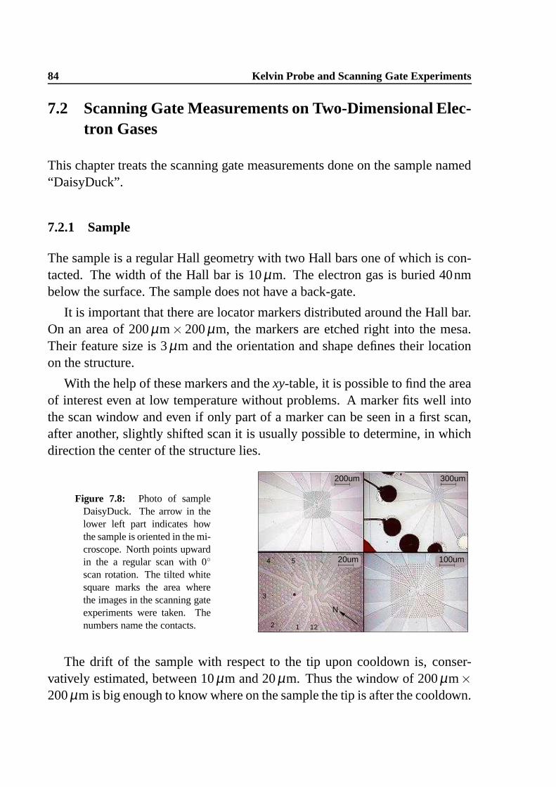
84 Kelvin Probe and Scanning Gate Experiments
7.2 Scanning Gate Measurements on Two-Dimensional Elec-tron Gases
This chapter treats the scanning gate measurements done on the sample named“DaisyDuck”.
7.2.1 Sample
The sample is a regular Hall geometry with two Hall bars one of which is con-tacted. The width of the Hall bar is 10 µm. The electron gas is buried 40nmbelow the surface. The sample does not have a back-gate.
It is important that there are locator markers distributed around the Hall bar.On an area of 200 µm× 200 µm, the markers are etched right into the mesa.Their feature size is 3 µm and the orientation and shape defines their locationon the structure.
With the help of these markers and the xy-table, it is possible to find the areaof interest even at low temperature without problems. A marker fits well intothe scan window and even if only part of a marker can be seen in a first scan,after another, slightly shifted scan it is usually possible to determine, in whichdirection the center of the structure lies.
Figure 7.8: Photo of sampleDaisyDuck. The arrow in thelower left part indicates howthe sample is oriented in the mi-croscope. North points upwardin the a regular scan with 0
scan rotation. The tilted whitesquare marks the area wherethe images in the scanning gateexperiments were taken. Thenumbers name the contacts. 1212
3
4 5
N
300um
100um20um
200um
The drift of the sample with respect to the tip upon cooldown is, conser-vatively estimated, between 10 µm and 20 µm. Thus the window of 200 µm×200 µm is big enough to know where on the sample the tip is after the cooldown.

7.2 Scanning Gate Measurements on 2DEGs 85
As the markers are imprinted onto the mesa, the effective resistances of theleads increase compared to a sample without any markers. But the density ofthe markers is not so high, that transport through the leads would be completelyinhibited.
0 2 4 6 8B [T]
0
5000
10000
15000
ρ xy[Ω
]
0
100
200
300
400
500
600
700
800
900
1000
ρ xx [Ω
]
3
12
5
4
1
Figure 7.9: Transport data ofsample “Daisy Duck”, mea-sured at T = 270mK.
Figure 7.8 shows a photograph of the sample in four magnifications. Thearrow on the lower left part shows how the orientation of the image can bebrought in accordance with the scans. The tip of the arrow points in the +y-direction of the scans.
Figure 7.9 shows the magneto-transport measurements done on the sampleat 270mK.
7.2.2 Scanning Gate Setup
In a scanning gate measurement the resistance between two contacts is mea-sured while the tip scans over the sample. The image plotted is the resistance asa function of the position of the tip.
The tilted white square in the lower left part of Fig.7.8 shows the area, wherethe following images were scanned. It was not possible to move the samplefurther to the left onto the Hall geometry and therefore the resistances had to bemeasured in a 3-terminal setup.
It was further not possible to change the potential of the tip. As it is possibleto change the potential of the whole sample with respect to the tip, this didnot add a major problem. Lifting the potential of the whole sample by U level
introduces only a slightly more difficult setup. Figure 7.11 shows the cablingof the subsequent experiment. It is important to keep U level
1 = U level2 =: U level

86 Kelvin Probe and Scanning Gate Experiments
at all times because otherwise a possibly high current flows through the sampleand might destroy it.
Figure 7.10: Kelvin probe ata distance of 40nm. Thequadratic fit again only holdsat negative bias voltages. Themaximum lies at about U=-2.2V. T = 4.2K.
-10 0 10U [V]
-800
-600
-400
-200
0
∆f [m
Hz]
data
fit
The potential of the tip could not be influenced directly, but from a Kelvinprobe experiment it is possible to determine the tip potential with respect tothe sample. This was done in Fig.7.10 and the data shows a maximum at U =
−2.2V. This is a shift of two volts compared to the data where the tip wasgrounded (see Fig.7.1 or Fig.7.5). One can thus assume that the potential of thetip is fixed at Utip = −2V.
Figure 7.11: The potential ofthe sample is lifted with respectto ground. The tip is at a con-stant potential. The 10MΩ re-sistor limits the sample current.
U1
Udrive Umeas
10MΩ
Sample
U2
level
level
The scanned images were taken with a resolution of 128 points per line and64 lines per scan. The scan range was always 8.8 µm× 8.8 µm scanned at aspeed of 500nm/s. With these parameters a scan takes 37 minutes.
The acquisition speed of the lock-in should correspond to the bandwidth ofthe scan. With the above scan parameters, one point is recorded every 0.13s.Therefore the current injected in the sample was 100nA at a frequency ofroughly 1kHz. The time constant of the lock-in could then be chosen to be30ms. This is sufficiently fast for the scan speed of 500nm/s, i. e., a time of130ms per point for a 8.8 µm scan range. An alternative would be to measuredc.

7.2 Scanning Gate Measurements on 2DEGs 87
7.2.3 Experimental Data
Figures 7.12 – 7.15 show five consecutive scans at the same sample position butwith different voltages U level applied to the sample. The voltage ranges from0V to −6.5V.
The topography in Fig.7.12 shows two markers. They consist of two squaresaligned along their diagonals. This indicates that the tip is positioned above arm1. The white square in Fig.7.8 shows where on the sample the images have beentaken. The area visible in the image is about 50% of the width of the wholevoltage probe 1.
50
100
150
200
0 2 4 6 80
1
2
3
4
5
6
7
8
x [µm]
y [µ
m]
1620
1622
1624
1626
1628
1630
1632
1634
1636
0 2 4 6 80
2
4
6
8
x [µm]
y [µ
m]
0 2 4 6 8162516301635
R[Ω
]0V
Figure 7.12: Left: Topography corresponding to the scanning gate measurement on theright. Right: Sample resistance. U level = 0. The horizontal stripes are an artifact of thedata processing done by the TOPS software. It was removed in the later scans. The inseton the lower end shows a line scan at y = 4.2 µm as indicated in the image. A positive“dip” at x = 5.8 µm is clearly visible. T = 270mK.
For the scanning gate images, the current runs through the contacts 1 and 4while the voltage is measured between 1 and 3. The graphs below the scanninggate images show a line scan along the x-direction at the positions indicated inthe scan. All images where taken at a temperature T = 270mK.
In the first topographic image, the marker is well visible. In the later imagesit seems as if a second, similar image was overlaid over the first. The reason isthat between Fig.7.12 and Fig.7.13 the shape of the tip must have changed toa double–tip, so that the topography was imaged with two tips simultaneously.The images are shifted by about 1 µm in x- and −2.5 µm in y-direction. Fromthe resistance image it is obvious that only one tip, namely the one responsible

88 Kelvin Probe and Scanning Gate Experiments
for the image at the lower edge of the scan range, is electrically relevant.
It happens frequently that during a scan, the tip picks up a grain of non-conducting material from the surface. During the process the shape of the con-ducting tip itself can change. The microscope then scans the sample with thenewly formed double tip and this results in two overlaid images.
1620
1622
1624
1626
1628
1630
1632
1634
1636
0 2 4 6 80
2
4
6
8
x [µm]
y [µ
m]
0 2 4 6 8162516301635
R[Ω
]
−1.5V
1560
1570
1580
1590
1600
1610
1620
1630
0 2 4 6 80
2
4
6
8
x [µm]
y [µ
m]
0 2 4 6 8158015851590
R[Ω
]
−3.0V
Figure 7.13: Two scanning gate measurements with U level = −1.5V on the left andU level = −3.0V on the right. The features of the topography disappear in the resistanceimage at this voltages.
7.2.4 Analysis
The scanning gate images show some interesting features. At the top of thetopography image in Fig.7.12 (left) a part of the next marker is visible. Thecurrent flows horizontally in the image in-between the two markers. On all butone (Fig.7.13, right) scanning gate images, an extremum in the resistance isvisible between the two markers.
At U level = 0,−1.5V (Fig.7.12, right and Fig.7.13, left), the resistance in-creases when the tip is between two markers. The feature disappears at U level =−3.0V (Fig.7.13, right) and at higher voltages, a minimum in the resistanceoccurs in the same position.
As mentioned earlier, the frame scanned in the images shows about half thevoltage probe carrying the current to the Hall bar. Therefore a considerablepart of the electrons have to go through the constriction imposed by the twomarkers. Hence, the influence of the tip on the current is biggest, when it isabove the constriction. A tip charged positively with respect to the 2DEG will

7.2 Scanning Gate Measurements on 2DEGs 89
attract electrons and more current carrying channels will be able to flow throughthe constriction. Consequently, the resistance decrease.
20
40
60
80
100
120
140
160
180
0 2 4 6 80
1
2
3
4
5
6
7
8
x [µm]
y [µ
m]
1615
1620
1625
1630
1635
0 2 4 6 80
2
4
6
8
x [µm]
y [µ
m]
0 2 4 6 8161016201630
R[Ω
]
−4.5V
Figure 7.14: Left: Topography. Obviously the shape of the tip has changed and a doubletip now scans the surface. Right: Corresponding resistance image. U level = −4.5V. Forthe first time, a feature of the topography is again visible in the resistance image. The dipis inverted, i. e., the resistance is lower, when the tip is above the marker, than when it isabove the 2DEG.
A tip negatively charged with respect to the electron gas will expel channelsand the resistance will increase.
By changing U level between two scans, it is thus possible to change the con-trast of the resistance image. This is very well visible in this series of images.
1730
1735
1740
1745
1750
0 2 4 6 80
2
4
6
8
x [µm]
y [µ
m]
0 2 4 6 8173017401750
R[Ω
]
−6.5V
Figure 7.15: Scanninggate measurement atU level = −6.5V.
The contrast switches occur at a voltage of about −3V. This correspondsroughly to the maximum in the Kelvin probe parabola measured earlier (Fig.7.10).At voltages above U level > −3V the tip is positively charged with respect to the

90 Kelvin Probe and Scanning Gate Experiments
sample. At voltages lower than U level = −3V the tip is negatively charged withrespect to the 2DEG.
This is a second, independent measurement showing that the tip potential isabout Utip = −2V. The Kelvin parabola shows a maximum at this voltage andthe resistance images show a contrast inversion.
One possible explanation might be the following. It was obviously not pos-sible to change the potential of the tip, i. e., the tip was not connected to thetop plug. The cable used to connect the tip is a semi-rigid thermo coax cable.It is known that these cables can act like batteries if not connected to a low-impedance source. This is especially true if some soldering acid or other liquidentered in-between in the outer and inner lead. Though a voltage of −2V israther high, this might at least in part explain the results.
The resistance within one scan at U level = 0 changes by about 35Ω. Thatis, when the tip is far away from the channel and thus does not influence theelectrons flowing in it, the overall resistance is about 35Ω smaller compared towhen the tip is above it.
At the position where the images have been taken, the complete width of thechannel is about 2 times the width seen in the topography. From the 4-terminalmeasurement of ρxx shown in Fig.7.9, one finds a sheet resistance of about 80Ωper square for the 2DEG.
Given that the electronic channel width visible in the image is about halfthe complete topographic channel width of the arm and given that the changein resistance is about half the 2DEG resistivity, one can deduce that the tipcompletely depletes the electron gas between the two markers. This correspondsto a circular depletion area with diameter of about 3 µm.
Note that the total resistance measured is about 1600Ω while the changesdue to the tip only amount to 35Ω. This is a change of only 2%. Therefore itis not possible to resolve finer structures in the resistance patterns. Had it beenpossible to measure the resistance in a 4-terminal setup, most probably a muchbetter resolution would have been achieved.

7.3 The Future 91
Not only the constriction between two markers can be mapped electronically,also the markers themselves show a distinct signature in the resistance image.In Fig.7.12 one sees a dip in the resistance image at the position of the markers.That is, the resistance increases when the tip is above the marker.
Lowering the potential of the sample as has been done in Fig.7.13 to −1.5Vand −3.0V, makes the dip disappear. Only at a lower voltage of −4.5V, thesignature of the markers reappears.
2DEG
tip
path
Figure 7.16: Schematic out-line of the path of the tip overa mesa edge. The sizes anddistances are approximately onscale. It is not a priori clear atwhat position the tip is electri-cally closest to the 2DEG.
This time the contrast is inverted as already seen in the above discussion.The contrast increases even further at the lower voltage of U level = −6.5V.
This feature is visible in both forward and backward scan. It can thereforenot be a artifact of the tip “jumping” over the mesa edge. Looking at Fig.7.16, itis nevertheless a priori clear, at which point the tip is closest to the 2DEG. Thegeometry of the tip as well as the depletion width and the depth of the 2DEGinfluence the resulting resistance traces.
Therefore not too much importance should be credited to the very shape ofthe feature, rather is it interesting that features as small as a mesa edge can beimaged with a tip that is geometrically much bigger than the resolution withwhich this can be achieved. This suggests that the electrically relevant part ofthe tip is much smaller than its geometrical size.
7.3 The Future
This thesis has shown that many interesting experiments are possible with thismicroscope. The low temperature combined with stability and reliability pro-vide a good starting point for interesting future experiments with local probes.

92 Kelvin Probe and Scanning Gate Experiments
Definitely, the work on Kelvin probe section could be extended to includemeasurements in magnetic fields.
Also the scanning gate measurements promise to be very interesting if amagnetic field is included. With an appropriate sample geometry, it should bepossible to image edge channels in the Quantum Hall regime.
With temperatures of 260mK it should be possible to see phase coherenceeffects. One of the very interesting experiments would definitely be a quantumpoint contact or even Aharonov-Bohm ring investigated with local probe micro-scope. The third candidate is a quantum dot showing Coulomb blockade. Thesamples would most probably be structures patterned with AFM lithography.
With the setup presented in this thesis, these projects came definitely in arange possible experiments and should be tackled as soon as possible.

Appendix A
Samples
A.1 List of Samples
The following table lists the samples used.
Name Description
Kos3b 2DEG, 37nm below surface. The sample was used for magnetic barrier mea-surements.
Aam 2DEG, 37nm below surface. The sample was used for the first force-distancemeasurements.
Daisy Duck 2DEG 40nm below the surface, Hall-bar imprinted onto the 2DEG. The sam-ple was used for scanning gate measurements.
A.2 Process Parameters
This appendix also gives detailed information on the processes used for definingthe Hall geometry and contacting the 2DEG. Our samples do not have gates.
A.2.1 Hall Bar
The Hall bar is defined by wet chemical etching.
• Positive photo resist Shipley S1805 is spun on the wafer at 4000rpm for1min.

94 Samples
• Resist is baked at 115 C for 2min.
• Exposure for 3.8s in the mask aligner defines the Hall geometry.
• Resist is developed for 45s in Shipley AZ.
• Clean water stops the process.
As the S1805 is a positive photo resist, the resist stays where no light reachesthe sample, i. e., the resist is there, where the Hall bar is intended to be.
• Subsequent etching in a solution of H2O:H2SO4:H2O2 = 100:3:1 (volumepercent) for 50s at 20 C removes the GaAs around the Hall bar.
• The remaining photo resist is removed by cleaning the sample in acetoneand isopropyl.
A.2.2 Ohmic Contacts
An alloy of AuGeNi is evaporated on the sample in order to define ohmic con-tacts.
• Negative photo resist Futurex NR1500 is spun on the wafer at 4000rpmfor 1min. Using negative photo resist permits undercut profiles which areneeded for the subsequent lift-off step.
• Resist is baked at 130 C for 1min.
• Exposure for 10s with the mask defining where the contacts will be.
• Resist is developed in Futurex RD2 for 3.5min. The resist remains outsidethe contacts.
• Dip etch in HCl for 15s.
• NiAuGe is evaporated on the sample in the following sequence:
37nm Ge
100nm Au
40nm Ni

A.3 Sample Cleaning 95
150nm Au
The ratio gold to germanium is Au : Ge = 88 : 12 (weight percent).
• Lift off: The alloy is removed around the contacts by solving the photoresist with acetone.
• Contacts are alloyed at 430 C for 2min in a hydrogen atmosphere.
A.3 Sample Cleaning
In order to be able to perform good scans, the surface of the sample has to bevery clean. Especially at low temperatures a grain as small as 0.5 micron canbecome an obstacle the tip can not overcome. This will result in local tip crashesthat can very well damage the tip.
It is therefore advisable to keep the samples in a clean place as long as pos-sible and expose it to ambient conditions only for short times. A very goodmethod to clean the sample once more after processing, but also when it hasbeen “at the Edge of the Wild” for longer times, is to put it in the plasma asherfor 10 minutes. The sample should then be cleaned in hydrochloric acid for notmore than 10 seconds and rinsed with clean water. Final drying with nitrogenis sufficient.


Appendix B
Conductive Heat Load and ThermalConductivities
The heat flow Q through a solid of a cross section A, under a temperature gra-dient dT/dx is given by
Q = kA · dTdx
where k is the (temperature dependent) thermal conductivity of the material. Ifthe two ends of a long section of this material (of length l) are held at tem-peratures T1 and T2, then the heat flowing from the warm to the cold end willbe
Q =Al
∫ T2
T1
k(T )dT =Al
k · (T2 −T1)
where k is the mean heat conductivity between the two temperatures. It is de-fined as
k =1
T2 −T1
∫ T2
T1
k(T )dT.
The thermal conductivities of manganine, constantan and steel used in oursetup are listed in Tab.B. As no values for the thermal conductivities for tem-
material k (300-4K) [W/cmK ] k (4-2K) [W/cmK ]
manganine 0.200 0.006constantan 0.200 0.006steel 0.109 0.003
Table B.1: Thermal conductivities of various metals.

98 Conductive Heat Load and Thermal Conductivities
peratures below 2K were available, the values for 2K were used instead for thecalculations below. As k drops with decreasing temperature, this should give anupper limit for the resulting heat loads.
The thermometers and sample cables are all made of constantan. The highvoltage cables for the stepper motors and the tube scanner are made of man-ganine of two different diameters and the six semi-rigid coax cables are forlow-noise measurements have a steel coating. Table B.2 lists all cables used.
count material diameter [mm]
300-4K:7 manganine 0.305 manganine 0.10
39 constantan 0.126 steel 0.50
4-1.5K:7 manganine 0.305 manganine 0.10
33 constantan 0.126 steel 0.50
1.5K- 300mK7 manganine 0.305 manganine 0.10
29 constantan 0.126 steel 0.50
Table B.2: Complete list of wires led to low-temperature parts of cryostat.
It is then easy to calculate the additional heat load originating from the wires.It was assumed that the thermal grounding at the three different stages wascomplete, i. e., the cables at the 4K-stage are really cooled to 4K.
In order to compare this to the original heat load the thermal conductance ofthe steel tubes was also estimated. The wall thickness had to be guessed and0.5mm for the thick and 0.25mm for the thin tubes seemed reasonable.
As can be seen from Tab.B.3, the heat load due to the cables only becomesimportant for the low-temperature parts. Compared to the original setup withminimal cabling a change of about 35% is calculated. This should reduce thehold time to about 65% of the specified 5 days. The hold time is the time atwhich the temperature of the 3He part is below 300mK. Indeed a hold time of 3days can be reached in a single shot without cooling the 1K-pot. If the magnet

99
Stage Qcables [W] Qtubes [W] ratio
300 - 4K 2.3 ·10−3 64.5 ·10−3 28.64-1.5K 7.2 ·10−6 16.6 ·10−6 2.21.5K- 300mK 3.1 ·10−6 2.3 ·10−6 2.3
Table B.3: Comparison of the heat loads due to cables and tubes.
is not swept and the xy- and z-stage are not used extensively, hold times of upto 5 days are feasible.


List of Symbols
In the following we want to give an incomplete list of all the abbreviations andsymbols used throughout this thesis.
Acronyms
2DEG two-dimensional electron gas
2DES two-dimensional electron sys-tem
AB Allen-Bradley (resistor)
ADC analog-digital converter
AFM atomic force microscopy
CPD contact potential difference
CuBe copper-berylium
DAC digital-analog converter
DOS density of states
HEMT high electron mobility transis-tor
ID inner diameter
IUC current-to-voltage converter
IVC inner vacuum chamber
LN2 liquid nitrogen
MBE molecular beam epitaxy
OD outer diameter
OVC outer vacuum chamber
PI proportional integral controller
PID proportional integral differentialcontroller
PLL phase locked loop
PZT lead zirconate titanate
S/N Signal to noise ratio
SEM scanning electron microscope
SFM scanning force microscopy
SNOM scanning near-field optical mi-croscopy
SPM scanning probe microscopy
SQUID superconducting quantum in-terference device
UHV ultra high vacuum
VCO voltage controlled oscillator
102 Conductive Heat Load and Thermal Conductivities
Symbols
2π Planck’s constant
2πωc cyclotron frequency
α∗ geometry factor
A vector potential
A area
α piezoelectric coupling of tuningfork
B external magnetic field
B magnetic field
Bz magetic field along z
C capacitance, usually tip-sample
CK stray (cable) capacitance
2D density of states in 2D
3D density of states in 3D
∆ f frequency shift
∆µch chemical potential difference
∆z tip-sample distance
δ z integrated noise in z
e electron charge
EF Fermi energy
Ed depolarization field
ε` energy of subband `
εn,` energy eigenvalues
ε1, ε2 dielectric constants
η degeneracy of a Landau level
φc critical angle
f0 resonance frequence of tuningfork
fzFB bandwidth of z-feedback
Ffric friction force
fg characteristic frequency of tu-ning fork
FN normal force
F2ω force at frequency 2ω
Fω force at frequency ω
Fts tip-sample force
fts f0 when tip interacting with sur-face
g g-factor
gs spin degeneracy
gv valley degeneration
I current
κ proportionality factor
K IUC conversion ratio
k cantilever stiffness
k thermal conductivity
` subband index

103
λF Fermi wavelength
m∗ effective electron mass
µB Bohr’s magneton
µch chemical potential
φ electrical potential
Ms saturation magnetization
µ friction coefficient
µdyn dynamic friction coefficient
µst static friction coefficient
ν filling factor of a Landau level
n Landau index
nHall ns extracted from Hall measure-ment
nSdH ns extracted from Shubnikov–de Haas measurement
ns electron sheet density
ω usually modulation frequency oflock-in
Q charge
Q quality factor
Q heat flow
Rxx longitudinal resistance
ρxx longitudinal resistivity
Rxy Hall resistance
ρxy Hall resistivity
τ general scattering time
T temperature
T transmission probability
TC Curie temperature
µelch electro-chemical potential
U tip-sample voltage
Uac ac-voltage
Udepl depletion voltage
Udc dc-voltage
UHall Hall voltage
U level potential by which the sample islifted
Uts tip-sample voltage
z tip-sample separation
This list does not claim to be complete.


Bibliography
[1] W.A. Aaia and C.C. Davis. A phase-locked shear-force microscope fordistance regulation in near-field optical microscopy. Appl. Phys. Lett.,70(4):405–407, 1997.
[2] D. Adams. The Hitchhiker’s Guide to the Galaxy, volume 1-5. Pan Books,1979. Don’t panic!
[3] T.R. Albrecht, P. Grütter, D. Horne, and D. Rugar. Frequency modulationdetection using high-Q cantilevers for enhanced force microscope sensi-tivity. J. Appl. Phys., 69(2):668–673, 1991.
[4] W. Allers, A. Schwarz, U.D Schwarz, and R. Wiesendanger. A scanningforce microscope with atomic resolution in ultrahigh vacuum and at lowtemperatures. Rev. Sci. Instr., 69(1):221–225, 1998.
[5] B.L. Altshuler and A.G. Aronov. Electron-Electron Interactions in Dis-ordered Systems, chapter 1, page 1 ff. Elsevier Science Publishers B.V.,1985.
[6] T. Ando, A.B. Fowler, and F. Stern. Electronic properties of two dimen-sional systems. Rev. Mod. Phys., 54:427–672, 1982.
[7] C.W.J. Beenaker and H. van Houten. Quantum Transport in Semiconduc-tor Nanostructures, volume 44 of Solid State Physics. Academic Press,1991.
[8] C.W.J. Beenakker and H. van Houten. Billard model of a ballistic multi-probe conductor. Phys. Rev. Lett., 63(17):1857–1860, 1989.
[9] S. Belaidi, P. Girard, and G. Leveque. Electrostatic forces acting on the tipin atomic force microscopy: Modelization and comparison with analyticexpressions. J. Appl. Phys., 81(3):1023–1030, 1996.

106 BIBLIOGRAPHY
[10] S.J. Bending and A. Oral. Hall effect in a highly inhomogeneous magneticfield distribution. J. Appl. Phys., 81(8):3721–3725, 1997.
[11] G. Binnig, C.F. Quate, and Ch. Gerber. Atomic force microscope. Phys.Rev. Lett., 56(9):930–933, 1986.
[12] G. Binnig, H. Rohrer, Ch. Gerber, and E. Weibel. Tunneling through acontrollable vacuum gap. Appl. Phys. Lett., 40(2):178–180, 1982.
[13] D.A. Brawner and N.P. Ong. Scanning Hall microprobe measurements ofmagnetization profiles in YBa2Cu3O7–y single crystals. J. Appl. Phys.,73(8):3890–3902, 1993.
[14] L.E. Bremme. Two-dimensional electron gases as sensors for magnetisa-tion measurements. Diplomarbeit, ETH Zürich, 1998.
[15] A.M. Chang, H.D. Hallen, L. Harriott, H.F. Hess, H.L. Kao, J. Kwo, R.E.Miller, R. Wolfe, J. van der Ziel, and T.Y. Chang. Scanning Hall probemicroscopy. Appl. Phys. Lett., 61(16):1974–1976, 1992.
[16] C.J. Chen. Introduction to Scanning Tunneling Microscopy. Oxford Uni-versity Press, 1993.
[17] E. Durand. Electrostatique, Tome II Problemes Generaux, Conducteurs.Masson &cie, 1966.
[18] U. Dürig, H.R. Steinauer, and N. Blanc. Dynamic force microscopyby means of the phase-controlled oscillator method. J. Appl. Phys.,82(8):3641–3651, 1997.
[19] U. Dürig, O. Züger, and A. Stalder. Interaction force detection in scan-ning probe microscopy: Methods and applications. Appl. Phys. Lett.,72(5):1778–1798, 1992.
[20] H. Edwards, L. Taylor, W.Duncan, and A.J. Melmed. Fast, high resolutionatomic force microscopy using a quarz tuning fork as actuator and sensor.J. Appl. Phys., 82(3):980–984, 1997.
[21] A.K. Geim, S.V. Dubonos, J.G.S. Lok, I.V. Grigorieva, and J.C. Maan.Ballistic Hall micromagnetometry. Appl. Phys. Lett., 71(16):2379–2381,1997.

BIBLIOGRAPHY 107
[22] S. Gider, J. Shi, D.D. Awschalom, P.F. Hopkins, K.L. Campman, A.C.Gossard, A.D. Kent, and S. von Molnár. Imaging and magnetome-try of switching in nanometer-scale iron particles. Appl. Phys. Lett.,69(21):3269–3271, 1996.
[23] F.J. Giessibl. Forces and frequency shifts in atomic-resolution dynamic-force microscopy. Phys. Rev. B, 56(24):16010–16015, 1997.
[24] F.J. Giessibl. High-speed force sensor for force microscopy and profilom-etry utilizing a quartz tuning fork. Appl. Phys. Lett., 73(26):3956–3958,1998.
[25] F.J. Giessibl. Atomic resolution on Si(111)-(7×7) by noncontact atomicforce microscopy with a force sensor based on a quartz tuning fork. Appl.Phys. Lett., 76(11):1470–1472, 2000.
[26] F.J. Giessibl, S. Hembacher, H. Bielefeldt, and J. Mannhart. Subatomicfeatures on silicon (111)-(7x7) surface observed by atomic forse mi-croscopy. Science, 289:422, 2000.
[27] R.D. Grober, J.Acimovic, J. Schuck, D. Hessman, P. Kindlemann, J. Hes-panha, A.S. Morse, K. Karrai, I. Tiemann, and S. Manus. Fundamen-tal limits to force detection using quartz tuning forks. Rev. Sci. Instr.,71(7):2779, 2000.
[28] P. Güthner, U.Ch. Fischer, and K. Dransfeld. Scanning near-field acousticmicroscopy. Appl. Phys. B, 48:89–92, 1989.
[29] H.D. Hallen, R. Seshadri, A.M. Chang, R.E. Miller, L.N. Pfeiffer, K.W.West, C.A. Murray, and H.F. Hess. Direct spatial imaging of vortices in asuperconducting wire network. Phys. Rev. Lett., 71(18):3007–3010, 1993.
[30] H. Hertz. Reine Angew. Math., page 156, 1881.
[31] K. Hjort, J. Söderkvist, and J.-Å. Schweitz. Gallium arsenide as a mechan-ical material. J. Micromech. Microeng., 4:1–13, 1994.
[32] H. Hölscher. Kontrastmechanismen in der Rasterkraftmikroskopie. Mas-ter’s thesis, University of Hamburg, 1999.

108 BIBLIOGRAPHY
[33] P. Horowitz and W. Hill. The Art of Electronics. Cambridge universitypress, 2nd edition, 1989. Chapter 5.9.
[34] H.J. Hug, B. Stiefel, P.J.A. van Schendel, A. Moser, S. Martin, and H.-J.Güntherodt. A low temperature ultrahigh vacuum scanning force micro-scope. Rev. Sci. Instr., 70(9):3625–3840, 1999.
[35] I.S. Ibrahim, V.A. Schweigert, and F.M. Peeters. Classical transport ofelectrons through magnetic barriers. Phys. Rev. B, 56(12):7508–7516,1997.
[36] I.S. Ibrahim, V.A. Schweigert, and F.M. Peeters. Diffusive transport in aHall junction with a microinhomogeneous magnetic field. Phys. Rev. B,57(24):5416–5427, 1998.
[37] T. Ihn. Elektrostatik einer leitfähigen AFM-Spitze über einer HalbleiterNanostruktur. Private notes, 2002.
[38] T. Ihn, T. Vancura, A. Baumgartner, P. Studerus, and K. Ensslin. Operationcharacteristics of a cryo-AFM feedback using high-Q tuning fork sensorsand a phase-locked loop. Rev. Sci. Instr., 2002.
[39] J. Israelachvili. Intermolecular and Surface Forces. Academic Press, Lon-don, 2 edition, 1992.
[40] J.D. Jackson. Classical Electrodynamics. John Wiley & Sons, 2nd edition,1975.
[41] H.O. Jacobs, H.F. Knapp, and A. Stemmer. Practical aspects of Kelvinprobe force microscopy. Rev. Sci. Instr., 70(3):1756–1760, 1999.
[42] R.J. Jelitto. Elektrodynamik. Number 3 in Theoretische Physik. AULA-Verlag, 3rd edition, 1994.
[43] M. Johnson, B.R. Bennet, M.J. Yang, M.M. Miller, and B.V. Shanabrook.Hybrid hall effect device. Appl. Phys. Lett., 71(7):974–976, 1997.
[44] K. Karrai and R.D. Grober. Piezoelectric tip-sample distance control fornear field optical microscopes. Appl. Phys. Lett., 66(14):1842–1844, 1995.
[45] K. Karrai and I. Tiemann. Interfacial shear force microscopy. Phys. Rev.B, 62(19):13174–13181, 2000.

BIBLIOGRAPHY 109
[46] M. Kato, A. Endo, S. Katsumoto, and Y. Iye. Two-dimensional electrongas under a spatially modulated magnetic field: A test ground for electron-electron scattering in a controlled environment. Phys. Rev. B, 58(8):4876–4881, 1998.
[47] Lord Kelvin. Philos. Mag. J. of Sci., 46(5):82, 1898.
[48] A.D. Kent, T.M. Shaw, S. van Molnár, and D.D. Awschalom. Growth ofhigh-aspect-ratio nanometer magnets with chemical-vapor-deposition andscanning-tunneling-microscopy. Science, 262:1249–1252, 1993.
[49] G. King and G. Nunes. By email. Private communications, 2001.
[50] V. Kubrak, B. Gallagher, and P. Main. Private communications.
[51] V. Kubrak, A.C. Neumann, B.L. Gallagher, P.C. Main, M. Henini, C.H.Marrows, and M.A. Howson. Longitudinal and Hall resistance induced bylarge-amplitude magnetic barriers. In Workbook of the Int. Conf. on theElectronic Properties of Two-Dimensional Systems (EP2DS), page 359,Ottawa, 1999.
[52] V. Kubrak, A.C. Neumann, B.L. Gallagher, P.C. Main, M. Henini, C.H.Marrows, and M.A. Howsen B.V. Shangbrook. Longitudinal and Hall re-sistance induced by large-amplitude magnetic barriers. Physica E, 6:755–758, 2000.
[53] L.D. Landau and E.M. Lifschitz. Lehrbuch der theoretischen Physik VII:Elastizitätstheorie. Akademie-Verlag Berlin, 1965.
[54] L.D. Landau and E.M. Lifshitz. Quantum Mechanics (Non-relativisticTheory), volume 3 of Course of theoretical physics, chapter §112 Motionin a uniform magnetic field, pages 456–458. Pergamon Press, 3rd edition,1977.
[55] D. Lange, M. Zimmermann, C. Hagleitner, O. Brand, and H. Baltes.CMOS 10-cantilever array for constant-force parallel scanning AFM. InTransducers 01, Digest of Technical Papers, pages 1074–1077. 2001.
[56] S. Liu, H. Guillou, A.D. Kent, G.W. Stupian, and M.S. Leung. Effect ofprobe geometry on the Hall response in an inhomogeneous magnetic field:A numerical study. J. Appl. Phys., 83(11):6161–6165, 1998.

110 BIBLIOGRAPHY
[57] C. Loppacher, M. Bammerlin, F. Battiston, M. Guggisberg, D. Müller,H.R. Hidber, R. Lüthi, E. Meyer, and H.J. Güntherodt. Fast digital elec-tronics for application in dynamic force microscopy using high-Q can-tilever. Appl. Phys. A, 66(7):S215–S218, 1997.
[58] G. Meier, M.Kleiber, D. Grundler, D. Heitmann, and R. Wiesendanger.Vertical polarization of quantum magnets in high density arrays of nickeldots with small height-to-diameter ratio. Appl. Phys. Lett., 72(17):2168–2170, 1998.
[59] W. Nabhan, B. Equer, A. Broniatowski, and G. De Rosny. A high-resolution scanning probe microscope for contact potential measurementson the 100nm scale. Rev. Sci. Instr., 68(8):3108–3111, 1997.
[60] M. Nonenmacher, M.P. o’Boyle, and H.K. Wickramsinghe. Kelvin probeforce microscopy. Appl. Phys. Lett., 58(25):2921–2923, 1991.
[61] A. Oral, S.J. Bending, and M. Henini. Real-time scanning Hall probemicroscopy. Appl. Phys. Lett., 69(9):1324–1326, 1996.
[62] A. Oral, S.J. Bending, and M. Henini. Real-time scanning Hall probemicroscopy. Appl. Phys. Lett., 69(9):1324–1326, 1996.
[63] S.H. Pan, E.W. Hudson, and J.C. Davis. 3He refrigerator based very lowtemperature scanning tunneling microscope. Rev. Sci. Instr., 70(2):1459–1463, 1999.
[64] F.M. Peeters and X.Q. Liu. Hall magnetometer in the ballistic regime.Appl. Phys. Lett., 72(5):572–574, 1998.
[65] F.M. Peeters and A. Matulis. Quantum structures created by nonhomoge-neous magnetic-fields. Phys. Rev. B, 48:15166–15174, 1993.
[66] F. Pobell. Matter and Methods at Low Temperatures. Springer, 1996.
[67] J. Reijniers and F.M. Peeters. Hybrid ferromagnetic/semiconductor Halleffect device. Appl. Phys. Lett., 73(3):357–359, 1998.
[68] W.H.J. Rensen and N.F. van Hulst. Atomic steps with tuning fork basednon-contact atomic force microscopy. Appl. Phys. Lett., 75(11):1640–1642, 1999.

BIBLIOGRAPHY 111
[69] A.G.T. Ruiter, J.A. Veerman, K.O. van der Werf, M.F. Garcia-Parajo,W.H.J. Rensen, and N.F. van Hulst. Tuning fork shear-force feedback.Ultramicroscopy, 71:149–157, 1998.
[70] A.G.T. Ruiter, J.A. Veerman, K.O. van der Werf, and N.F. van Hulst. Dy-namic behavior of tuning fork shear-force feedback. Appl. Phys. Lett.,71(1):28–30, 1997.
[71] J. Rychen. Combined Low-Temperature Scanning Probe Microscopy andMagneto-Transport Experiments for the Local Investigation of MesoscopicSystems. Dissertation, Swiss Federal Institute of Technology, Zürich,2000. Diss. ETH No. 14119.
[72] J. Rychen, T. Ihn, P. Studerus, A. Herrmann, and K. Ensslin. A low-temperature dynamic mode scanning force microscope operating in highmagnetic fields. Rev. Sci. Instr., 70:2765, 1999.
[73] J. Rychen, T. Ihn, P. Studerus, A. Herrmann, K. Ensslin, H.J. Hug, P.J.A.van Schendel, and H.J. Güntherodt. Force-distance studies with piezoelec-tric tuning forks below 4.2K. Appl. Surf. Sci., 157(4):290–294, 2000.
[74] J. Rychen, T. Ihn, P. Studerus, A Herrmann, K. Ensslin, H.J. Hug, P.J.A.van Schendel, and H.J. Güntherodt. Operation characteristic of piezoelec-tric quartz tuning forks in a high magnetic fields at liquid helium tempera-tures. Rev. Sci. Instr., 71(3):1695, 2000.
[75] D. Sarid. Scanning Force Microscopy. Oxford University Press, 1994.
[76] U.D. Schwarz, O. Zwörner, P. Köster, and R. Wiesendanger. Quantitativeanalysis of the frictional properties of solid materials at low loads. i. carboncompounds. Phys. Rev. B, 56:6987–6996, 1997.
[77] R. Steinke, M. Hoffmann, M. Böhmisch, J. Eisenmenger, K. Dransfeld,and P. Leiderer. Potentiometry with the acoustic near field microscope: Anew method for microscopy of surface potentials. Appl. Phys. A, 64:19–27,1997.
[78] S.T. Stoddart, S.J. Bending, A.K. Geim, and M. Henini. Quantum-resolvedinvestigations of flux dynamics: Collective and single vortex effects. Phys.Rev. Lett., 71(23):3854–3857, 1993.

112 BIBLIOGRAPHY
[79] U. Tietze and Ch. Schenk. Halbleiter Schaltungstechnik. Springer, Berlin,1999. 11. Ausgabe, Kapitel 14.2.
[80] U. Tietze and Ch. Schenk. Halbleiter Schaltungstechnik. Springer, Berlin,1999. 11. Ausgabe, Kapitel 24.2.2.
[81] M. Todorovic and S. Schultz. Magnetic force microscopy utilizingpiezoresistive cantilever. J. Appl. Phys., 83(11):6229–6231, 1998.
[82] M.A. Topinka, B.J. Leroy, R.M. Westervelt, S.E.J. Shaw, R. Fleischman,E.J. Heller, K.D. Maranowski, and A.C. Gossard. Coherent brached flowin a two-dimensional electron gas. Nature, 410:183–186, 2001.
[83] T. Vancura. Nanolithography by local anodic oxidation of shallowGa[Al]As heterostructures using an atomic force microscope. Diplomar-beit, ETH Zürich, 1997/98.
[84] T. Vancura, T. Ihn, S. Broderick, K. Ensslin, W. Wegscheider, and M. Bich-ler. Electron transport in a two-dimensional electron gas with magneticbarriers. Phys. Rev. B, 62:5074, 2000.
[85] K. von Klitzing, G. Dorda, and M. Pepper. New method for high-accuracydetermination of fine-structure based on quantized Hall resistance. Phys.Rev. Lett., 45:494, 1980.
[86] Klaus von Klitzing. The quantized Hall effect. Rev. Mod. Phys.,58(3):519–531, 1986.
[87] Chr. Wittneven, R. Dombrowski, S.H. Pan, and R. Wiesendanger. A low-temperature ultrahigh-vacuum scanning tunneling microscope with rotat-able magnetic field. Rev. Sci. Instr., 68(10):3806–3810, 1997.
[88] M.J. Yoo, T.A. Fulton, H.F. Hess, R.L. Willett, L.N. Dunkleberger, R.J.Chichester, L.N. Pfeiffer, and K.W. West. Scanning single-electron tran-sistor microscopy: Imaging individual charges. Science, 276:579–582,1997.

Danksagung
Eine Dissertation ist selten das Werk einer Einzelperson. So ist auch diese Ar-beit nur dank der Hilfe vieler Menschen möglich geworden.
An erster Stelle danke ich Klaus Ensslin für die Möglichkeit, ein so komple-xes Projekt zu realisieren. Seine stete Hilfe und sein Enthusiasmus haben miroft geholfen, die technischen Schwierigkeiten auf dem Weg zu bewältigen.
Des Weiteren danke ich Thomas Ihn für die Unterstützung und die vielenIdeen, die er einbrachte. Theorie und Interpretation zu den magnetischen Bar-rieren stammen ebenso wie die Rechnungen zur “Phase Locked Loop” haupt-sächlich aus seiner Feder. Zudem steuerte er wichtige Ideen zur Entwicklungdes Mikroskops bei. An seinem ersten Entwurf wurden während des Baus im-mer nur kleine Erweiterungen und Verbesserungen vorgenommen.
Während des letzten Jahres war Slavo Kicin eine grosse Hilfe. Er machteeinen grossen Teil der Arbeit zu den Kelvin-Probe Experimenten.
Die Entwicklung und der Bau der Elektronik und vor allem das Auffindenunzähliger Fehler in der “Oxford Kiste” waren das Werk von Paul Studerus.Auch sein Beitrag zum Funktionieren des Mikroskops ist unschätzbar.
Cecil Barengo verbrachte unzählige Stunden mit der Installation und demUnterhalt des Kryostaten und der Vakuumtechnik. Besonders dankbar bin ich,dass er mir die Zeichnungen des Mikroskops gemacht und angepasst hat.
Bei Stefan Lindemann bedanke ich mich für die Zusammenarbeit am Elek-tronenstrahlmikroskop während des ersten Jahres unserer Dissertation.
Unsere Sektretärin, Brigitte Abt, übernahm den administrativen Teil und istmassgeblich für die gute Atmosphäre in der Gruppe verantwortlich.
Ebenfalls danke ich bei meinen Kollegen Silvia Lüscher, Ryan Held, JörgRychen, Sebastian Brosig, Gian Salis, Rainer Jäggi, Andreas Fuhrer, Volkmar

114 Danksagung
Senz, August Dorn und Christoph Ellenberger für die gemeinsame Zeit. Beson-ders Andreas Baumgartner wünsche ich viel Erfolg mit seinem Mikroskop. Ichhoffe, mein Nachfolger Alessandro Pioda wird viele interessante Messungenmit Janis machen können.
Die Mannschaft der Werkstatt unter Peter Brühwiler hat hervorragende Ar-beit beim Bau des Einzelteile geleistet. Geschwindigkeit und Präzision, mit wel-chen die Teile gefertigt wurden, überraschten uns immer wieder aufs Neue.
Die Schwingungsdämpfung des Mikroskop war nur dank der Ideen und desTatendrangs von Jean-Pierre Stucki möglich.
Hans-Ruedi Scherrer danke ich, dass er die vielen Proben bedampfte, die ichzu Beginn der Arbeit machte.
Viel Arbeit nahmen mir Beat Rubischon, Daniel Schönenberger und ElmarHeeb ab, indem sie die Betreuung des Fileservers übernahmen.
Zuletzt dürfen auch folgende Leute nicht ungenannt bleiben: Lisi, Edy, En-zo, Florentine, Sören, Anita, Walter, Trudi, Regula, Rita, Cyril, Heidi, Giampi,Silvia und Antonín.

Curriculum Vitae
Tobias Vancura, geboren am 28.12.1973 in Kaiserslautern, Deutschland. Bürgervon Vechigen (BE), Schweiz.
Zivilstand: ledigEltern: Antonín und Silvia VancuraGeschwister: Cyril
Ausbildung1980 – 1984 Grundschule Pestalozzi, Kaiserslautern, Deutsch-
land.1984 – 1993 Staatliches Gymnasium an der Burgstrasse, Kai-
serslautern.10/1993 – Grundstudium Physik an der Universität Kaisers-
lautern.10/1995 Hauptstudium an der ETH Zürich, Schweiz.seit 8/1998 Doktorarbeit am Laboratorium für Festkörperphy-
sik in der Gruppe von Prof. K.Ensslin an der ETHZürich.


Curriculum Vitae
Tobias Vancura, born Dec 28th, 1973 in Kaiserslautern, Germany. Citizen ofVechigen (BE), Switzerland.
Marital status: unmarriedParents: Antonín and Silvia VancuraSiblings: Cyril
Education1980 – 1984 Pestalozzi Primary School, Kaiserslautern, Ger-
many.1984 – 1993 High School, Staatliches Gymnasium an der Burg-
strasse, Kaiserslautern.10/1993 – Grundstudium in Physics at University of Kaisers-
lautern.10/1995 Hauptstudium at ETH Zurich, Switzerland.since 8/1998 PhD thesis at Laboratory of Solid State Physics in
the group of Prof. K.Ensslin at the ETH Zurich.