ring-down techniques of a-si:h using in-situ cavity ... · pdf filein thin film growth from...
TRANSCRIPT
9Studies into the Growth Mechanism
of a-Si:H Using in-situ CavityRing-Down Techniques
M. C.M. van de Sanden, I.M.P~ Aarts, J.P.M. Hoefnagels, B. Hoex,R. Engein and WM.M. Kessels
Department ofApplied Physics, Eindhoven University of Technology, The Netherlands
9.1 Introduction
In thin film growth from the vapor phase, a flux of gas phase species impinges on a substrateand reacts with the surface to deposit a film. The deposition techniques utilized to grow thinfilms may involve both physical and chemical processes [1,2]. For example, in physicalvapor deposition (PVD) [3], typically individual atoms or perhaps small clusters of atomsthat originate from a liquid or solid source impinge on a solid surface to which they stick andform a thin film. Surface reactions are commonly induced by the reactive nature of theatoms, while the substrate is often held at room temperature. In contrast, in chemical vapordeposition (CVD) a film is usually deposited from a (stable) gas that undergoes a chemicalreaction at the surface induced by the substrate temperature [1]. In this process, heating ofthe substrate is generally used to activate and control the chemical reactions of the precursorgas. Our interest lies in a specific kind of CVD, in which the film growth takes place byreactive gas phase species as, for example, created with a plasma or a hot filament (plasmaenhanced CVD or hot-wire CVD, respectively). Key to these deposition methods is thefact that the dissociation of the precursor gases basically takes place in the gas phase, whichgenerally results in a large variety of reactive gas phase molecules, atoms, radicals, and ions.
caviO’ Ring-Down Speciroscopy: Techniques and Applications Edited by Giel Berden and Richard Engeln© 2009 Blackwell Publishing, Ltd

238 Cavity Ring-Down Spectroscopy: Techniques and Applications
As a consequence, gas phase activation of the precursor gases enables the deposition ofhighquality films at lower substrate temperatures than those typically used in conventionalCVD. Alternatively, thin-film synthesis by means of gas phase activation of precursors mayalso share PVD-like processes, such as surface bombardment by energetic gas phase speciesand shadowing effects.
In this chapter we will discuss our efforts in recent years to unravel the growth mechanismof hydrogenated amorphous silicon (a-Si:H) from reactive gas phase species, formed eitherby plasma or by a hot wire in silane gas possibly diluted with hydrogen gas. The growth ofhydrogenated amorphous silicon films serves in this case as a model system for thin filmgrowth from vapor-based processes. Hydrogenated amorphous silicon is an importantmaterial as it is the basis of next generation thin film solar cells and of thin film transistors,which are utilized in active matrix liquid crystal displays.
In general, the growth process of thin films can be broken down in three aspects, whichinclude the gas phase composition, the surface composition, and the film properties, asschematically illustrated in Figure 9.1 for the case of hydrogenated amorphous silicon.These aspects may exhibit strong mutual correlations, while they are also influenced bytheir internal physical and chemical processes. As an example, for plasma enhanced CVD,the chemical nature the surface as well as the radical or ion determines the reaction at thesurface [4]. On the other hand, the surface chemical nature itself is determined by thegoverning reactions that take place at the surface. This example illustrates that, in order tounderstand the thin film growth process, the following general research questions should beanswered:
Reactive gas phase species(molecular radicals and ions)
Surface composition
Film composition(density, defects, morphology, etc.)
~ ro~je~a~.’’a’r~v~r ~c ..~! ~ ~ (a J:h)
Figure 9.1 Schematic representation of the growth process of thin films. The different aspectsof the growth process, which include the gas phase composition, the surface composition, andthe film properties, are shown on the right. (See plate section for a colour representation)

Studies into the Growth Mechanism of a-Si:H 239
• What are the relevant gas phase species for the growth process?• What are the microscopic surface reaction steps (of these gas phase species) that lead to
film growth?• How are the film properties determined by these gas phase species and their surface
reactions?
It is evident that these questions cannot be answered completely within the context of thischapter. Moreover, the answers to these questions depend on the particular growth processconsidered and, in that respect, the choice of a-Si :H from reactive species can be consideredas a model system. However, the questions posed will serve as a guide to structure thechapter and are used to illustrate the strength of cavity ring down techniques to provide(partial) answers to these questions. As such we do not aim at a complete picture of thegrowth mechanism of a-Si:H; for this we refer to earlier publications by our group andothers (http:/!www.phys.tue.nl/pmp).
Schematically the content of this chapter is illustrated in Figure 9.2. We will start with adiscussion of the density and flux measurement of various silane radicals as measured in situin a plasma. Determination of the gas phase densities may be a real challenge for plasma-enhanced and hot-wire CVD due to the diverse composition of (reactive) species that istypically created through a variety of gas phase reactions. Apart from the flux of species to
1~ U/e ~~~::::plasma with
radical species
HR mirror HR mirror
1998
transparentHR mirror film substrate HR mirror
~ detector~ 2001
film ~evanescent
wavefoldedcavity ______________
2004
HR mirror HR mirror detector
Figure 9.2 The development of the cavity ring-down technique to study the growth mechanismof a-Si:H at the Eindhoven University of Technology in the Plasma and Materials Processinggroup
240 Cavity Ring-Down Spectroscopy: Techniques and Applications
the surface, it is also necessary to know the species’ surface reactivity to establish therelevance of a species for film growth. Often, a species that is very reactive at the surface hasa relatively low gas phase density, because it is easily lost at the surface. Therefore, despiteits low density, its relevance for the growth process may be great. This calls for sensitivegas phase diagnostics, such as cavity ring-down absorption spectroscopy, that are able todetect low—density reactive species. These measurements are very similar to other gas phasemeasurements using cavity ring-down using a linear cavity and are aimed at measuring thedensity and flux of the specific radical. To determine the surface reaction probability of tworadicals that are important for growth, in this case the silyl (SiH3) and the silicon (Si) radical,we have employed time dependent cavity ring-down spectroscopy, which is the next subjectwe will discuss in this chapter.
To answer the question ‘What are the microscopic surface reaction steps that lead to filmgrowth?’ it is necessary to study the growth surface exposed to the reactive plasma or hot-wire gas phase, and in particular to address the role of the surface dangling bond. As wasconcluded from, for example, attenuated total reflection Fourier transform JR spectroscopy and other studies of the a-Si:H growth surface, a-Si:H is almost completelypassivated by atomic hydrogen. Therefore the dangling bond is considered to be theprimary reactive site where radicals attach. To test the feasibility of the detection of surfacedangling bonds, we first had to make an excursion into the detection of dangling bondsin condensed matter systems. For this we used a linear cavity into which we introducedan high quality optical flat, on which an a-Si:H film was deposited (see Figure 9.2). Aswill be demonstrated, we achieved a dangling bond detection sensitivity that iscomparable to present day condensed matter standards such as, for instance, photothermaldeflection spectroscopy. Moreover, we demonstrated the applicability of the condensedmatter version of cavity ring-down spectroscopy for the detection of other low-densityimpurities, such as Erbium in substoichiometric oxide films [5]. Finally, in the foldedcavity geometry, in collaboration with Pipino from the National Institute of Standards andTechnology (NIST) and utilizing a high quality quartz truncated prism, measurementsof the surface dangling bond density during silane hot wire CVD of a-Si:H could beperformed.
The outline of this chapter is as follows. Section 9.2 deals with the CRDS detection ofSiH~ radicals, including the time dependent version of CRDS to measure the surfacereaction probability of Si and SiH3. In Section 9.3 we will discuss thin film or condensedmatter CRDS to detect low concentration species in thin films, such as dangling bonds ina-Si:H. Section 9.4 discusses the measurement of dangling bonds employing evanescentwave CRDS with a folded cavity.
9.2 Gas Phase CRUS on SiH~ Radicals
9.2.1 Production and Loss Processes of Radicals Under Plasma Conditions
For basic understanding and modeling of plasma or radical based deposition (or etching)processes, information on the density as well as the surface reactivity of the plasma speciesis essential. The density of a specific radical under plasma conditions is the resultof production and loss processes. The latter comprises both gas phase losses as well as

Studies into the Growth Mechanism of a-Si:H 241
surface losses. The density n~ follows from the balance equation (neglecting radical-radicalreactions):
OflxpLpflx (9.1)
with n~ the radical density, F the production, and L the loss processes. The loss rate ç’ isexperimentally accessible by observing the decay time of the radical density after switchingoff the production process P rapidly. In the stationary state it follows from Equation (9.1)that the density n~ is a direct result of both production as well as loss processes:
n~ = P-r~ (9.2)
It should be realized that a pure exponential decay should be observed only if higher orderloss processes in the gas phase are absent. Although the radical and ion density are importantaccessible parameters in processing plasmas, knowledge on the loss rate is essential tounderstanding the role of the radical or ion in the deposition or etching process. The reason isthat a part of the loss process is directly proportional to film growth or etching. Furthermore,measurement of the loss rate ~ 1 can reveal whether a radical is important in the depositionor etching mechanism or is mainly lost in the gas phase due to chemical reactions.
If the loss process is a purely surface loss process, the loss rate ~ 1 includes, apart fromthe loss rate associated with transport (diffusion or convection), the so-called surfacereaction probability f3. This surface reaction probability is defined as the probability that theradical in interaction with the surface is lost, i.e. it contributes to film growth or etching or itis transformed into another gas phase species. The surface reaction probability of coursedepends on both the chemical (presence of reactive sites) and physical state (for exampleroughness) of the surface and the specific radical considered. Measuring the loss probability/3 therefore provides information on the surface science of deposition and etching processesunder plasma conditions and a comparison with dedicated molecular dynamics calculationsbecomes possible. In this section we will limit ourselves to the SiH3 and Si radical duringthe growth of silicon thin films.
Often the surface reaction probability /3 of the species is obtained indirectly [6] or underprocess conditions different from the actual plasma deposition process, e.g., from amolecular beam scattering experiment [7] or by time-resolved density measurements inan afterglow plasma [8,9]. We here discuss the use of time-resolved cavity ring-downspectroscopy (t-CRDS) to obtain /3 during plasma deposition: the highly sensitive cavityring-down spectroscopy (CRDS) method is used to map an increased radical density due toa pulsed rf bias to the substrate in addition to the continuously operated remote SiH4 plasma.Although time-resolved CRDS has been employed previously to obtain gas phase lossrates of radicals [10,11], in this work the technique has been extended to measurements ofthe surface loss rates of the radicals [12]. This yields, simultaneously, information on thesurface reaction probability /3 and the density of the radicals under the specific plasmaconditions, in this chapter particularly for the case of high rate deposition of hydrogenatedamorphous silicon (a-Si:H). Using this method, it has been shown that Si is mainly lost in thegas phase to SiH4, whereas SiH3 is only lost via diffusion to, and reactions at, the surface.Moreover, /3 of Si and SiH3 are determined and it is shown that /351H3 is independent of thesubstrate temperature.

242 Cavity Ring-Down Spectroscopy: Techniques and Applications
9.2.2 Experimental Set-Up for Plasma Deposition of a-Si:Hand CRDS Measurements
A schematic representation of the plasma set-up that is used to study the deposition ofa-Si:H is shown in Figure 9.3(a). It consists basically of three elements: the expanding
0Time >‘
Figure 9.3 (a) The expanding thermal plasma (ETP) set-up equipped with the cavity ring-downspectroscopic set-up, an rf power supply for pulsed bias voltage application to the substrate,and an additional delay generator to synchronize the pulsing of the laser to the pulsing of the rfpower supply. (b) Schematic time diagram illustrating the modulation of the radical density andthe synchronization of the CRDS laser pulses (Reprinted with permission from Hoefnagels etal.,Time-resolved cavity ringdown study of the Si and SiH3 surface reaction probability duringplasma deposition of a-Si:H at different substrate temperatures;]. App!. Phys. 2004, 96, 4094.Copyright 2004, American Institute of Physics)
I
rf power on
rf power off I I II IAt
ETP+rf density
steady-state —
A
ETP density
0 A Alaser pulses
® 0(b)

Studies into the Growth Mechanism of a-Si:H 243
thermal plasma (ETP) reactor in which the SiH4 plasma is created, the cavity ring-downspectroscopy set-up, and the various additional components necessary to carry out the time-resolved measurements.
9.2.2.1 The Expanding Thermal Plasma
The ETP reactor consists of a cascaded arc plasma source and a low-pressure depositionchamber. In the cascaded arc, a current controlled d.c. discharge at 22.5 A is maintained at~bar using an Ar and H2 flow of 27.5 and 2.5 sccs (standard cubic centimeter persecond), respectively. The d.c. discharge produces thermal Ar—H2 plasma that expands intothe deposition chamber. By regulating the pumping speed, the pressure in the reactor can becontrolled between 0.09—0.54 mbar, corresponding to a residence time in the reactor of~0.4—2.4 s. At about 5 cm from the arc exit, a pure SiH4 flow of 0.5—2.5 sccs is injected intothe expanding plasma. Due to the expansion, the electron temperature is reduced toapproximately 0.1—0.3 eV and, therefore, electron-induced dissociation of SiH4 can beneglected. Instead, the SiH4 is dissociated by reactive ionic or atomic species emanatingfrom the plasma source. Under the conditions used in this section, atomic hydrogen isdominates the dissociation of SiH4 leading mainly to the creation of SiH3 radicals. Si andother radicals are also produced, but at a much lower rate, leading to a much lower density.The SiH4 plasma flows towards a substrate with an area of 10 x 10cm2, located 35 cm fromthe arc exit. Under the conditions used in this section, ion bombardment can be neglectedas the low electron temperature leads to a small floating potential of —2 V of the a-Si:Hsurface [13j, while there are indications that the flux of atomic hydrogen towards thesubstrate is relatively low compared with the flux of the silane radicals. The substratetemperature can be accurately controlled from room temperature to 450 °C. Heating ofthe substrate by the plasma is reduced to less then 15°C from its starting temperature, due togood thermal contact between the substrate and the substrate holder by means of a smallhelium back flow.
9.2.2.2 The Cavity Ring-Down Spectroscopy Set-Up
The optical cavity of the CRDS set-up has a length of 108cm and is created using two highlyreflective mirrors (radius of curvature r —1.0 m, reflectivity R 0.99 at 251 nm for thedetection of Si and SiH3, see below), positioned on either side of the plasma reactor.The configuration is detuned from confocal so that a quasi-continuous mode structureinside the cavity is obtained. This enables a relatively straightforward wavelength tuning byscanning the wavelength of the laser. The mirrors are connected to the reactor via bellowsthat allow for fine-adjustment. Two valves (not shown) are placed between the mirrors andthe vessel to protect the mirrors during cleaning of the vessel. A small argon flow is usuallysupplied through the valves to protect the mirrors during plasma operation. A SirahPrecisionscan D dye laser, pumped by a Nd:YAG laser (Spectra Physics, Quanta RayDCR1 1), is operated on a Coumarin 500 dye in order to produce 10Hz, 6—7 ns laser pulsesat ~-.~502 nm that are frequency doubled by a beta-barium borate crystal to ~25 1 nm with aline width of ~‘-~ 1.0 pm. The dye laser is temperature stabilized to within 0.1 °C to control thewavelength consistently within~pm. After passing a neutral-density filter to reduce thelight intensity, the laser pulses are introduced into the CRDS cavity. The light intensity inthe cavity decays exponentially due to intrinsic cavity losses and possible absorption losses.

244 Cavity Ring-Down Spectroscopy: Techniques and Applications
Light, leaking out of the cavity through the second mirror, is detected by a photomultiplier(Hamamatsu R928) after passing an interference band-pass filter centered at 250 nm to
F reduce stray light. Every CRDS transient is individually digitized and processed (i.e. aweighted least-squares fit to the logarithm of the transient) by means of a state-of-the-art100 MHz, 12-bit data acquisition system (TUJeDACS, which has a maximum repetition rate
V of 2 kHz [20]) yielding the exponential decay time of the light intensity in the cavity.A measurement of the difference in this decay time with and without a plasma as a function
7 of the laser wavelength yields the absorption spectrum of the plasma in absolute sense.Dividing the absorption values by the absorption cross-section yields the line-integrated
IF density of the species. When the radial density profile has also been determined, thespatially resolved radical density in front of the substrate can be computed directly from theline-integrated density.
The cavity is aligned at an axial position of about 5 mm from the substrate in order toprobe the radicals directly in front of the substrate. SiH3 has been measured at the broadbandA2A’1 ~— X~A~ transition (cf. Figure 9.4(a)) at a wavelength of ‘-~.~250 nm and its density hasbeen quantified by the cross-sectional data reported by Baklanov et al. [14] and Lightfootet al. [15]. The ground state Si density has been determined from measurements at the4s 3Po,1~2 ~— 3p~ 3P012 transitions at 250.7 nm, 251.4nm and 251.9nm, using the Einsteinabsorption coefficients reported (cf. inset Figure 9.4(a)) [16]. Also discussed below is thetotal SiH density, which has been deduced from measurements of the Qi(11 .5) rotationalline of the SiH A 2~ ~ X 2~-~ band at ~414 nm using information on the cross-section andpartition function available in LIFBASE (cf. Figure 9.4(b)) [17]. For these measurements,light at 414 nm was obtained from the same pulsed dye laser as above, but now operating onExalite 411. The ring-down mirrors had a reflectivity of 0.996 and a radius of curvatureof—i m [18].
9.2.2.3 Time-Resolved CRDS Measurements
In a time-resolved CRDS (t-CRDS) measurement, the radical density close to the substrateis modulated by applying pulsed if power to the substrate, while the time evolution of theabsorption induced by the if-generated radicals is mapped using CRDS. To apply if powerto the substrate, a Hewlett Packard 81 16A function generator is used to create a 20.1 MHzsine wave signal. The signal is subsequently amplified by a 10-watt and 100-watt amplifier(Henry Electronics 100B-30) and is impedance matched to the substrate holder by a L-typematching network. The forward power, measured with a Bird 4410A power meter betweenthe amplifier and matching network, was kept constant at 63 watt, unless stated otherwise,while the reflected power was reduced to < 0.1 watt for all measurements. The d.c. biasvoltage on the substrate, as measured with a high voltage probe, is typically between —50 Vand —100 V for the plasma settings used in this chapter. A Stanford DG535 delay generatoris used to gate the function generator in order to generate 5-Hz if pulses with a duty cycle of,typically, 2.5 %. It is noted that the d.c. bias voltage falls off within 20 ~ts after the if power isturned off, as has been measured with the high voltage probe. In this way a minor periodicmodulation of the radical density is produced in addition to the continuous production ofradicals in the ETP. The duty cycle of 2.5 % has been carefully chosen in order to obtain agood signal-to-noise ratio in the additional Si and SiH3 absorption, while possible powderformation due to the ‘anion confining’ if plasma sheath is suppressed [19]. The additional

(0Cl)(0
a,
00.0(I,
0.0
Studies into the Growth Mechanism of a-Si:H 245
412.5 413.0 413.5
Wavelength (nm)
Figure 9.4 (a) Parts of the SiH3 absorption spectrum of the A2A +— .Y?2A1 electronic transition,as measured in the ETP compared to the normalized absorption spectra as reported by Baklanovet a!. [14] and Lightfoot et a!. [15], both given in arbitrary units. Inset: absorption lines of the4~3 P ~— 3p2 3P transition ofSi around 251 nm, superimposed on the broadband SiH3 spectrum
(dashed line) (Reprinted with permission from Hoefnagels et al., Time-resolved cavity ringdownstudy of the Si and Si!-!3 surface reaction probability during plasma deposition of a-Si:H atdifferent substrate temperatures; I. App!. Phys. 2004, 96, 4094. Copyright 2004, AmericanInstitute of Physics). (b) Measured (bottom) and simulated (top) SiH ground state absorptionspectrum of the A 2~ x 2j~ band at ~4 14 nm. For the simulation the LIFBASE program wasused. A rotational temperature of 1800K and a vibrational temperature of3000 K resulted in thebest correspondence (Reprinted with permission from Kessels et al., Cavity ring down study ofthe densities and kinetics ofSi and SiH in a remote Ar-H2-Sil-14 p!asma;J. AppI. Phys. 2001, 89,
2065. Copyright 2001, American Institute of Physics)
absorption A~ due to the radicals generated by the if pulse is obtained from the differencein absorption at some point.~1 tin the rf afterglow and at a point long after the influence of theif pulse has extinguished [cf. Figure 9.3(b)]. As mentioned before, every CRDS trace ishandled separately by means of a ‘state-of-the-art’ 100-MHz, 12-bit data acquisition
IL.) • •1 I,
250.69 251.61251.92
I ° L.A SH3 absorption
0o~-”------
AETPu Baklanov eta!. (in au.)0 Lightfoot et a!. (in au.)
0200
(a)220 240 260 280
Wavelength (nm)
-&;~ 1.5Cl)(00.
~ 1.0C0
~0.5
(b)
414.0 414.5

246 Cavity Ring-Down Spectroscopy: Techniques and Applications
system [20] and an averaged A,f is obtained as a function of the time ~Xt in the afterglow ofthe rf pulse.
9.2.3 Cavity Ring-Down Measurements During ETP Deposition of a-Si:H
9.2.3.1 SiH3, SiH and Si Density in an Expanding Thermal Plasma
The Si, SiH3, and SiH densities in the plasma depend on the dilution ratio, which is defined
7’ as the ratio of the H2 flow to the SiH4 flow. In the experiments the SiH4 flow, which was11 injected via a ring around the Ar/H2 plasma expansion [see Figure 9.3(a)], has been varied7 while the H2 flow was fixed at 30 sccs. The Ar—H2 plasma, produced upstream in the
cascaded arc, was used to dissociate SiH4. Under high H2 dilution conditions, deposition ofnanocrystalline silicon occurs at high rates (up to 3 nmls) [21]. The pressure in the reactorwas maintained at ‘—450 mtorr (~—~20 Pa).
In Figure 9.5, the results for the densities of the SiH3, SiH and Si radicals are given asfunctions of the dilution ratio. It is clearly seen that under conditions of low dilution, whichis actually the amorphous silicon deposition conditions, the silyl radical (SiH3) is the
f dominant radical. For higher dilution ratios (the film becomes nanocrystalline (nc-Si:H) fordilution ratios higher than 50) the importance of other radicals in the gas phase such asSi and SiH becomes apparent. The relatively higher importance of the Si and SiH radicalsin the gas phase is due to the fact that more hydrogen abstraction reactions of silane withatomic hydrogen (generated in the plasma source, the cascaded arc) take place withincreasing hydrogen dilution. However, to discuss the relevance of these radicals for thedeposition of the silicon thin films (either in the amorphous or nanocrystalline case),information is needed on their contribution to film growth. This depends not only on theirgas phase density but also on the reaction probability at the growing film surface. Tomeasure these reaction probabilities time-dependent CRDS can he employed, which will bediscussed next.
i&~ %• ““I””””.
1O12 - +
~ S~H -
0,~
I io~ -I I II it Ii I III liii1 10 50 100 150 200
7 Dilution ratio H2/S1H4
Figure 9.5 The SiH3, SIH and Si density as function of the dilution ratio H2/S1H4 in anexpanding thermal plasma in an Ar/H2/S1H4 mixture
L

Studies into the Growth Mechanism of a-Si:H 247
9.2.3.2 Sutface Reaction Probability and Loss Rate of Si and SiH3 Determinedwith t-CRDS
To test the influence of if power on the radical density in front of the substrate, theabsorption of Si and SiH3 has been measured with CRDS at about 5 mm from the substrate,while the FTP plasma was operated under standard conditions. The results of twoabsorption spectra recorded with and without if power applied to the substrate are shownin Figure 9.6. The spectra clearly show that both the Si line-absorption and the broadbandabsorption due to SiH3 increase due to the rf power. This demonstrates that the radicaldensity in front of the substrate is indeed higher as compared with the standard operatingcondition of the FTP, when if power is applied to the substrate.
The result of a typical ‘r-CRDS measurement for Si and SiH3 is illustrated in Figure 9.7,which shows that both Si and SiH3 decrease single exponentially, which is expected fromthe radicals’ mass balance [22]:
(9.3)
As mentioned before, the corresponding loss rate r~ depends linearly on the gas phase losson one hand and the loss due to diffusion to and reactions at the surface on the otherhand [22]:
= krny~~ (9.4)
4 I
(0(I)
0.
~ 2
1 en0(000~o,oe~
ETP0n 0
ETPoff 0
0~I
250.68 250.69 250.70Wavelength (nm)
Figure 9.6 Two CRD spectra recorded with (top) and without (bottom) rfpower applied to thesubstrate. The spectra show the narrow band line absorption due to the Si 4s3P2 3p2 3f~transition superimposed on the broad band SiH3 A2A’1 ~— ~A1 absorption. At the start andend of each scan, the plasma has been turned off to obtain the baseline loss of the CRD cell(Reprinted with permission from Hoefnagels et a!., Time-resolved cavity ringdown study ofthe Si and SiH3 surface reaction probability during plasma deposition of a-Si:H at differentsubstrate temperatures;]. App!. Phys. 2004, 96, 4094. Copyright 2004, American Institute ofPhysics)
248 Cavity Ring-Down Spectroscopy: Techniques and Applications
5 x 1 O~
Cl)0Cl)
0
~- io-~00.0
5 x i ~-4
0.0 0.2 0.4
Time a~t (ms)
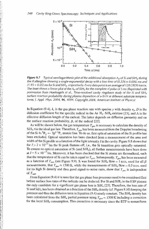
Figure 9.7 Typical semilogarithmic plot of the additional absorption A~i ofSi and SiLl3 duringthe rfafterglow showing a single exponential decay with a loss time of (0.226 ± 0.006) ms and(1.93 ± 0.05) ms for Si and SiH3, respectively. Every data point is an average of 128 CRDS traces.The inset shows a linear plot of the Aff ofSiH3 for the complete rfpulse of5 ms (Reprinted withpermission from Hoefnagels et al., Time-resolved cavity ringdown study of the Si and SiH3surface reaction probability during plasma deposition of a-Si:H at different substrate temperatures; J. Appl. Phys. 2004, 96, 4094. Copyright 2004, American Institute of Physics)
In Equation (9.4), kr is the gas phase reaction rate with species y with density n~, D is thediffusion coefficient for the specific radical in the Ar—H2—SiH4 mixture [23], and A is theeffective diffusion length of the radical. The latter depends on diffusion geometry and onthe surface reaction probability, f3, of the radical [22].
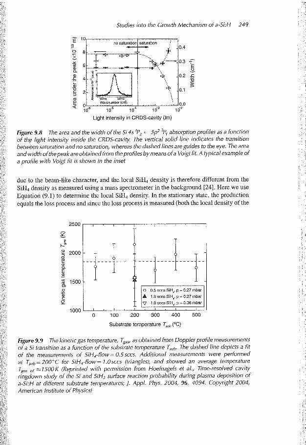
As will be shown below, the gas temperature Tgas is necessary to calculate the density ofSiH4 via the ideal gas law. Therefore, Tgas has been measured from the Doppler broadeningof the Si 4s 3P2 ~— 3p2 3P1 atomic line. To do so, first optical saturation of the Si profile hasbeen excluded. Optical saturation has been checked from a measurement of the area andwidth of the Si profile as a function of the light intensity un the cavity. Figure 9.8 shows thatfor 1> 2 x i0~ im the Si peak flattens off, i.e., the Si transition gets optically saturated.To ensure no optical saturation of Si (and SiH3), all further measurements have been doneat 1=5 x 1 0~ im. Moreover, it has been checked that the Si atoms are thermalized, suchthat the temperature of Si can be taken equal to Tgas. Subsequently, Tgas has been measuredas a function of TSUb (see Figure 9.9). It was found for SiH4 flow — 1 sccs, used for all /3measurements, that Tg~~ 1500K, while the measurements of SiH4 flow 0.5 sccs, usedfor its high Si density and thus good signal-to-noise ratio, show that Tgas is independentof T~11b.
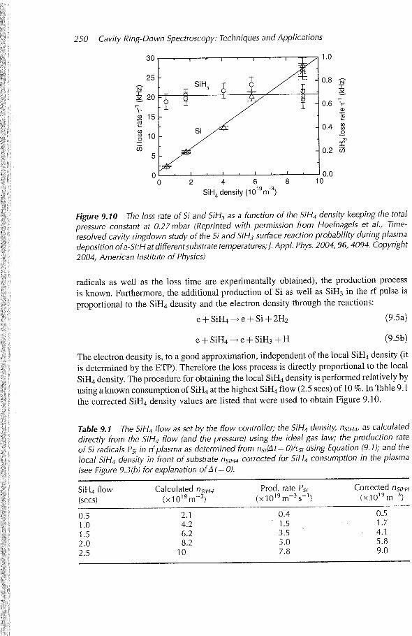
From Equation (9.4) it is seen that the gas phase loss processes need to be considered firstbefore surface loss rates of the radicals can be deduced. For Si and SiH3 in the ETP plasmathe only candidate for a significant gas phase loss is SiH4 [23]. Therefore, the loss rate ofSi and SiH3 has been obtained as a function of the SiH4 density (cf. Figure 9.10) keeping thepressure and thus the diffusion term in Equation (9.4) nearly constant. The SiH4 density hasbeen calculated from the SiH4 partial pressure using Tgas = 1500 K including a correctionfor the local SiH4 consumption. This correction is necessary since the ETP is nonuniform
0.6 0.8 1.0
~ie8~)
x
Cs 6a>
a)
a)
CSa)
I.I~I~I,I• I
.-*___0 0.5 sccs SiR4, p = 0.27 mbarA 1.0 sccs SiR4, p = 0.27 mbar
V 1.0 sccs SIR4, p = 0.36 mbarI I I I • I I
Substrate temperature ‘~sub ‘ S.’,
Figure 9.9 The kinetic gas temperature, Tgas, as obtained from Doppler profile measurementsof a Si transition as a function of the substrate temperature T3~b. The dashed line depicts a fitof the measurements of SiH4—flow = 0.5 sccs. Additional measurements were performedat Tuub200°C for SiH4-flow= 1.Osccs (triangles), and showed an average temperatureTgas c~ 1500 K (Reprinted with permission from Hoefnagels et a!., Time-resolved cavityringdown study of the Si and SiH3 surface reaction probability during plasma deposition ofa-Si:H at different substrate temperatures; I. AppI. Phys. 2004, 96, 4094. Copyright 2004,American Institute of Physics)
Studies into the Growth Mechanism of a-Si:H 249
no saturation
5 39749 39750Wavenumber (cr~1)
saturation /
-~
*
0.4
0.3~EC)
0.2 -~-o
0.1
fin
ict6 io~ io~ i~ id2Light intensity in CRDS-cavity (Im)
Figure 9.8 The area and the width of the Si 4s 3P2 ~— 3p2 3P1 absorption profiles as a functionof the light intensity inside the CRDS-cavity. The vertical solid line indicates the transitionbetween saturation and no saturation, whereas the dashed lines are guides to the eye. The areaand width of the peak are obtained from the profiles by means ofa Voigt fit. A typical example ofa profile with Voigt fit is shown in the inset
due to the beam-like character, and the local SiH4 density is therefore different from theSiH4 density as measured using a mass spectrometer in the background [24]. Here we useEquation (9.1) to determine the local SiH4 density. In the stationary state, the productionequals the loss process and since the loss process is measured (both the local density of the
2500
2000ci)Daa)0.Ea)Cl)cci0)0
a)0
10000 100 200 300 400 500
250 Cavity Ring-Down Spectroscopy: Techniques and Applications
G)
000
0)
Table 9.1 The SiH4 flow as set by the flow controller; the SiH4 density, nSIH4, as calculateddirectly from the S1H4 flow (and the pressure) using the ideal gas law; the production rateof Si radicals P51 in if plasma as determined from ns1k.~ t— 0)/rs1 using Equation (9.1); and thelocal S1H4 density in front of substrate nSIH4 corrected for SiH4 consumption in the plasma(see Figure 9.3(b) for explanation of i~t= 0).
S1H4 flow Calculated nsIH4 Prod. rate P51 Corrected nSIH4
(sccs) (x1019 m3) (xl 019 m ~ s~) (x1019 m3)
0.5 2.1 0.4 0.51.0 4.2 1.5 1.71.5 6.2 3.5 4.12.0 8.2 5.0 5.82.5 10 7.8 9.0
N
‘P
0 2 4 6 8SIH4 density (1019 m3)
1.0
0.8 -~
0.6 ‘~-
0,J.’~ 00
C’)z
0.2 0)
0.010
Figure 9.10 The loss rate of Si and SiH3 as a function of the SiH4 density keeping the totalpressure constant at 0.27 mbar (Reprinted with permission from Hoefnagels et al., Time-resolved cavity ringdown study of the Si and SiH3 surface reaction probability during plasmadeposition ofa-Si:H at different substrate temperatures;]. AppI. Phys. 2004, 96, 4094. Copyright2004, American Institute of Physics)
radicals as well as the loss time are experimentally obtained), the production processis known. Furthermore, the additional production of Si as well as SiH3 in the if pulse isproportional to the SiH4 density and the electron density through the reactions:
e+SiH4—~e+Si+2H2 (9.5a)
eH-SiH4—~e+SiHa+H (9.5b)
The electron density is, to a good approximation, independent of the local SiH4 density (itis determined by the ETP). Therefore the loss process is directly proportional to the localSiH4 density. The procedure for obtaining the local SiH4 density is performed relatively byusing a known consumption of SiH4 at the highest SiH4 flow (2.5 sccs) of 10 %. In Table 9.1the corrected SiH4 density values are listed that were used to obtain Figure 9.10.

Studies into the Growth Mechanism of a-Si:H 251
As can be seen in Figure 9.10 the loss rate of SiH3 is independent of the SiH4 density,which indicates no gas phase loss of SiH3, while the loss rate of Si increases linearly withthe SiH4 density. The slope reveals a reaction rate constant of Si(3P) with SiH4 ofk1 = (3.0 ± 1.3) x 10 16m3 s~ This value corresponds well with literature values [12].
Finally, to deduce the surface reaction probability /3 of Si and SiH3 from Equation (9.1), asemi-empirical expression, as proposed by Chantry [22], can be assumed for the cylindersymmetrical diffusion geometry of the ETP reactor. Then, for SiH3 (no gas phase loss) theloss time t~ in Equation (9.4) depends linearly on the pressure with a slope depending onthe radial and axial diffusion lengths and Tgas and an offset depending on the radial andaxial diffusion lengths, Tgas, and /3. If the diffusion of radicals in radial direction can beneglected in respect to the diffusion in axial direction, i.e., the radial diffusion length goes toinfinity [12], which is the case in the experiments discussed in this section, the axialdiffusion length, H, can be obtained from the pressure dependence of the loss time of SiH3.
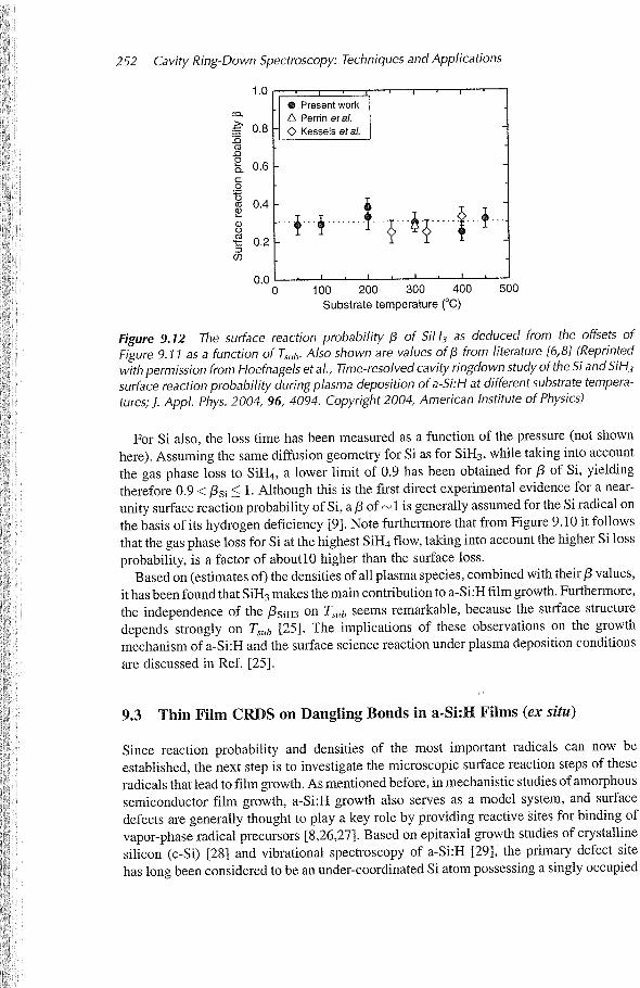
The loss time of SiH3 has been measured as a function of the pressure for six differentsubstrate temperatures, see Figure 9.11. Based on the independence of Tgas on ~ all theindividual data sets in Figure 9.11 can be fitted simultaneously with a shared slope toEquation (9.4) to obtain better accuracy in H. Then, from the six offsets in Figure 9.11, thesurface reaction probability /3 can be obtained as a function of T~11b (Figure 9.12). No cleardependence of l3siH3 on T~~b is seen. Apparently, all values of f3SiH3 can be averaged,yielding f3SiH3 0.30 ± 0.03. This value is in good agreement with estimated values of/3SiH3 for three different Ts11b as obtained previously with the indirect method of ‘aperturewell assembly’ applied under similar conditions in the same set-up. The value alsocorresponds to /3SiH3 = 0.28 * 0.03 at T~1~b 300 °C, as determined by Perrin et al. usingtime-resolved threshold ionization mass spectrometry in an if plasma with a 100 % on—offmodulation [8].
Cl)2
a)2Cl)0)0
(I)
40 50
Figure 9.11 The SiH3 loss time, determined by time-resolved cavity ring down experiments,as a function of the total pressure for six different substrate temperatures and for a constant SiH4flow (Reprinted with permission from Hoefnagels et al., Time-resolved cavity ringdown studyof the Si and SiLl3 surface reaction probability during plasma deposition of a-Si:H at differentsubstrate temperatures; J. Appl. Phys. 2004, 96, 4094. copyright 2004, American Institute ofPhysics)
0 10 20 30Pressure (Pa)
252 Cavity Ring-Down Spectroscopy: Techniques and Applications
in ______________• Present workL~ Perrin eta!.
~ ~ Kessels eta!.-DCo
0.4
~ ...+~.+ ~I I
Ci)
0.0 I
0 100 200 300 400 500Substrate temperature (°C)
Figure 9.12 The surface reaction probability j3 of SiH3 as deduced from the offsets ofFigure 9. 11 as a function of T5~b. Also shown are values of 1~3 from literature [6,8] (Reprintedwith permission from Hoefnagels et al., Time-resolved cavity ringdown study of the Si and SiH3surface reaction probability during plasma deposition of a-Si:H at different substrate temperatures; J. App!. Phys. 2004, 96, 4094. Copyright 2004, American Institute of Physics)
For Si also, the loss time has been measured as a function of the pressure (not shownhere). Assuming the same diffusion geometry for Si as for SiH3, while taking into accountthe gas phase loss to SiH4, a lower limit of 0.9 has been obtained for /3 of Si, yieldingtherefore 0.9 </35j ~ 1. Although this is the first direct experimental evidence for a near-unity surface reaction probability of Si, a /3 of ‘-.~ 1 is generally assumed for the Si radical onthe basis of its hydrogen deficiency [9]. Note furthermore that from Figure 9.10 it followsthat the gas phase loss for Si at the highest SiH4 flow, taking into account the higher Si lossprobability, is a factor of aboutlO higher than the surface loss.
Based on (estimates of) the densities of all plasma species, combined with their /3 values,it has been found that SiH3 makes the main contribution to a-Si:H film growth. Furthermore,the independence of the /3SiFJ3 on T~11b seems remarkable, because the surface structuredepends strongly on ~ [25]. The implications of these observations on the growthmechanism of a-Si:H and the surface science reaction under plasma deposition conditionsare discussed in Ref. [25].
9.3 Thin Film CRDS on Dangling Bonds in a-Si:H Films (ex situ)
Since reaction probability and densities of the most important radicals can now beestablished, the next step is to investigate the microscopic surface reaction steps of theseradicals that lead to film growth. As mentioned before, in mechanistic studies of amorphoussemiconductor film growth, a-Si:H growth also serves as a model system, and surfacedefects are generally thought to play a key role by providing reactive sites for binding ofvapor-phase radical precursors [8,26,27]. Based on epitaxial growth studies of crystallinesilicon (c-Si) [28] and vibrational spectroscopy of a-Si:H [29], the primary defect sitehas long been considered to be an under-coordinated Si atom possessing a singly occupied
L

Studies into the Growth Mechanism of a-Si:H 253
sp3-hybridized orbital or ‘dangling bond’ (DB), which binds radical precursors through afacile radical—radical coupling [30]. However, the bulk DB density in device-grade a-Si:H istypically 1016 cm ~, while a surface defect density as low as 1011 cm2 is conceivablycompatible with DB-based growth mechanisms. Therefore, highly sensitive in-situ techniques are required to probe DB defects and yield decisive mechanistic insight. Moreover,there is a need to measure dangling bonds absolutely on the growth surface in real-time andin situ. This is, however, challenging, since a simple calculation shows that expectedabsorptions are small and cannot be measured using a simple, one-pass, direct absorptiontechnique. Assuming a surface coverage of about 101 ‘cm2 (corresponding to an approximate 10~ dangling bond coverage) and a cross-section of 10 ‘6cm2 one can readilycalculate absorptions to be in the l0~~ range. Depending on the surface kinetics involved(Eley—Rideal, Langmuir—Hinshelwood or Kisliuk type kinetics) [31], this dangling bondcoverage could be significantly lower.
The dangling bond in the bulk of a-Si:H is one of the dominant defects and can bemeasured using several sensitive film diagnostic techniques [32]. Presently used detectionschemes for defect spectroscopy, such as photothermal deflection spectroscopy (PDS) orthe constant photocurrent method, are very sensitive but indirect [3 3,34], which means thatthey require a calibration procedure and cannot be used in real time during film growth.Electron spin resonance (ESR) is a very sensitive technique and Das et al. have employed itin situ by adapting the plasma system so that it fits in an ESR cavity [35]. Therefore,new diagnostics, which are preferably direct and ‘all optical’ are of great use in this field,as well as in thin film technologies in general. In this section we will show defect-relatedmeasurements using CRDS. The difference with the previously discussed CRDS detectionscheme is that now the investigated sample is a thin film deposited on a substrate (seeFigure 9.13). The absorption by dangling bonds [(cf. Figure 9.15(a)] in the sample is in the0.7—1.3 eV range, as can be seen in Figure 9.15(b), where the absorption coefficient is givenas function of energy. The potential of CRDS in measuring bulk defects is shown bymeasuring defect-related absorption in relatively thin a-Si:H films of 4—98 nm thickness.This proof of principle of measuring bulk defects in a-Si:H is the first step towards in situand real-time detection of dangling bonds during growth.
The extension of CRDS to the condensed matter (cm-CRDS) was first proposed and
demonstrated by Engein et al. [36,37], and was soon followed by others [38,39]. In thisvariant ofCRDS, it is most convenient to distinguish three different loss terms that determinethe intensity decay of the light inside the cavity: (i) intrinsic losses due to the cavity,~inherent to the mirrors finite reflectivity; (ii) absorption and scattering losses induced by thesubstrate, Lsubstrate, and (iii) the absorption and scattering losses due to the film, Lfil,7,. Allscattering and absorption losses are, in principal, dependent on the wavelength w of thelight. Equation (9.6) gives the ring-down time -r in terms of the round-trip losses, ZL~(w),
i.e. the sum of the three loss terms, generated in the cavity and the roundtrip time tr for lightin the cavity
( ) — tr — t1 (96)W — Z L1(w) — Lcavj0(~) + Lsubsrrate(&)) + Lffl,fl(w)
From Equation (9.6) it follows that by measuring the ring-down time -r, the losses can bedirectly calculated while differential measurements can be used to obtain the losses causedby the substrate or film separately.
254 Cavity Ring-Down Spectroscopy: Techniques and Applications
9.3.1 General Considerations
In the experiments discussed in this section the substrate has been placed perpendicularlyto the incident light pulse (cf. Figure 9.13), as other reported possibilities such as usingthe minor as a substrate or placing the substrate under the Brewster angle are notoptions [38,39]. For example, the Brewster-angle scheme has the clear disadvantages thata single Brewster angle is ‘ill-defined’ for a substrate-film configuration, therefore notleading to unit transmission, while the scheme is also only sensitive for one polarizationdirection. A perpendicular position of the substrate is generally applicable without cleardisadvantages caused by the substrate-film reflectivity (see below).
In this section we explore the effects related to the insertion of an optical flat into a stablelinear optical resonator formed by two planoconcave minors. The stability criteria of theresonator, the time dependence of the light leaking out of the resonator upon excitation,and the position of the optical flat with respect to the resonator mode structure is analyzed.The roughness of an optical flat or a thin film-substrate system induces light scattering,which might influence the absorption in a cm-CRDS measurement. Available literatureon scattering theory from rough surfaces, where we limit ourselves to total integratingscattering experiments, are used to evaluate the influence on the absorption measurementsduring cm-CRDS. Furthermore, we will address the expected sensitivity of an optimizedcm-CRDS configuration when the considerations addressed are properly taken into accountin the design of the optical set-up and absorption experiment.
9.3.1.1 Validity and Design Criteria for crn-CRDS
A concern when applying CRDS to condensed media is the influence of the insertion ofan optical flat (a thin-film substrate or crystal) on the stability of the optical resonator.Obviously, the surface roughness of the optical flat should be low enough to assure that astable optical resonator can be maintained. For a crystal this can be reached by anappropriate polishing of the optical surfaces, the surface roughness of thin films is usuallya result of the growth process. The influence of the surface roughness on the cm-CRDSexperiment is treated in detail below. For the analysis that follows we assume that thesurfaces of the optical flat are perfectly smooth and normal to the optical axis of theresonator.
The stability of optical resonators has been investigated previously [40]. Within theparaxial approximation, the resonator optical properties can be described using a round-tripmatrix representation M,~. The sequence of matrices M1, associated with each element ofthe resonator, define M~:
Mrt = M1M2M3 . . . Mn = (9.7)
For an empty resonator formed by two planoconcave mirrors separated by a distance I andradius of curvature r, M,.~ is given by:
11 10 11 10M,.1=~0 1~x~2 ~x~0 x~2 1H
I •~~• ~
4(L-r)
r2
2l(r—l)
~ r , (9.8)r

Studies into the Growth Mechanism of a-Si:H 255
where the first and third matrices represent a translation over a distance 1 and the second andfourth matrices represent a reflection of the light beam from the planoconcave mirror. Thestability condition of the resonator can be written as a constraint on the trace of Mrt [40],given by:
(9.9)
This leads, for the Mrt in Equation (9.8), to the stability criterion 1 < 2r, for which low-diffraction-loss modes are supported in the resonator. For a resonator with an optical flat ofthickness h and refractive index n, placed at a distance p from a high-reflective concaveinput mirror and distance q from a high-reflective concave output mirror, the overallresonator system now consists of three coupled resonators: (i) two planoconcave resonators,formed by the concave mirror and the optical flat; (ii) the optical flat itself (Fabry—Perotresonator), and (iii) the high-finesse resonator formed by the two planoconcave mirrors.The resonators (i), (ii), and (iii) should all be considered in terms Of Mrt to acquire the overallstability conditions. For resonators (i) Equation (9.9) reads Ii — 2p/rI ~ 1 and 1 — 2qIrI ~ 1,which leads to a stability criterion p ~ r and q ~ r. The Fabry—Perot resonator, (ii) , is acritically stable resonator, and as long as the interfaces are parallel to each other the systemis stable for every h. However, diffraction losses are inevitable but can be reduced bydecreasing h. The high-finesse resonator, (iii) , has a total length of p + h + q, for whichthe stability condition is given by p + h + q < 2r. Acknowledging that p and q must besmaller than r, two different cases can be distinguished. If the total resonator length is lessthan r, then the optical flat can be placed at any position inside the cavity, or, if the resonatorlength is between r and 2r, the position of the optical flat is limited to an area aroundthe center of the resonator to enforce p ~ r and q ~ r. In common situations and for ease ofalignment the central position in the optical resonator is usually chosen.
Compared with an empty resonator, the optical flat will disturb the spatial and temporalelectric field build-up within the resonator, especially when the reflectivity of the opticalflat Rflat is relatively high compared with the mirror reflectivity R,njrm,. This perturbationwill also affect the recorded transient from which the ring-down time in Equation (9.6) isextracted, and consequently may influence the accuracy of the determination of ‘r as well.In order to explore the influence of the optical flat, the temporal output of the resonatorshould be calculated. This requires detailed knowledge on the coupling coefficientsbetween the individual resonators. The calculation can be simplified by considering thatmany modes are excited in the resonator, in which case averaging allows the coupling to betreated by standard Fresnel transmission and reflection coefficients. Furthermore, thetransverse beam profile is assumed to be stationary such that the problem can be treated asone dimensional along the optical axis. Using both assumptions the evolution of the lightintensity output of a resonator can be calculated by summing the individual electric fieldintensities of all possible light paths, present at the output mirror at a specific time t. Theanalytical equations for the resonator output intensity can be found in Ref. [41].
To illustrate the field intensity build-up and its influence on the ring-down time, we haveperformed a simple round trip calculation using Fresnel coefficients for the interfaces of themirrors and an infinitesimal optical flat (single surface). For a resonator with length
0.30 m, a mirror reflectivity of Rmirror 0.995 and an optical flat with reflectivity Rpat,positioned at the center of the resonator, the calculated transients for various Rflat are

256 Cavity Ring-Down Spectroscopy: Techniques and Applications
Idler:infrared
Figure 9.13 The set-up used to perform CRDS on thin films
depicted in Figure 9.14. The values taken refer to typical values used in the experimentsdescribed in the following section. For Rfla( = 0.01 the transient is still single exponentialand has the expected ring-down time of 200 ns [Equation (9.6)]. For increasing Rflat, aconsiderable deviation from the unperturbed system is observed, especially during thebuild-up phase of the resonator. This can be understood by considering that for large Rflat thelight is initially confined to the resonator formed by the input mirror and the optical flat,impeding its reaching the output mirror at short time scales, which is reflected by the initialsmaller output intensity when compared with the almost unperturbed system with Rflat =0.01. Nevertheless, even for the extreme case of Rflat = 0.98, after roughly one ring-downtime or 200 ns, the resonator shows a similar decay rate as observed for the unperturbedsystem.
C,)
D
cci>~
Cl)Cci)C
600
Figure 9.14 The light output of a resonator with 1=0.3 m upon excitation with a laser lightpulse ofs ns duration for different values of the reflectivity of the optical flat, Rcat, is shown. Largedeviations of the transient from a single-exponential decay occur for reflectivities above 0.9,well beyond typical experimental values for R~at. The arrows show optimal cursor settings foran accurate determination of the ring-down time
40cm
Time (ns)

Studies into the Growth Mechanism of a-Si’:H 257
Conduction band!1.7 j 10.1
> A1 o~ - band to band•5. / transitions
- ~ 10~ - Tail statesj
00
io-~- DB
Valence band \ I I
DOS (log N) 0.5 1.0 1.5 2.0 2.5Photon Energy (eV)
(a) (b)
Figure 9.15 (a) The density ofstates (DOS) ofa-Si:H, where the arrows indicatepossible opticaltransitions. The related absorption spectrum is given in (b). Below a photon energy of 1.4ev;the optical transitions are dominated by defect-related absorptions, i.e., the absorption valuesgive information on the dangling bond (DB) density. Between photon energies of 1.4eV and1.7ev; the absorption is mainly dominated by transitions involving tail states. Above 1.7ev;direct band gap transitions determine the absorption spectrum
From a practical point of view, the determination of the ring-down time is moreaccurately obtained if the first part of the decay (largest signal) can be used in order tocircumvent the small signal and correspondingly large relative uncertainty in the last part ofthe transient. Figure 9.14 illustrates that if the reflectivity, Rflat of the optical flat is less than0.5, the transient has the typical single exponential decay over the full sampling region,which is indicated by arrows. In this case the ring-down time can be accurately ascertained.For Rflat> 0.9, the first part of the transient is seriously affected by the perturbation ofthe optical flat and a good determination of the ring-down time becomes problematic oreven impossible. However, in common circumstances, for instance when considering a thinfilm—substrate system, the reflectivity of the optical flat remains well below 0.9 and thering-down can be extracted without difficulties from the transient.
Another effect related to the insertion of an optical flat into the resonator, is an increase ofthe optical resonator length, which increases the round-trip time and consequently the ring-down time as well. As a result, the measurement overestimates the absorption of the opticalflat. To estimate the influence of this effect the change in the resonators’ refractive indexshould be evaluated, which can be given by:
~empty 1 + ~(fljiar12einpty) (9.10)
where ~ is the refractive index for the empty resonator, and h is the thickness of theoptical flat. For example, if the optical flat has a thickness, h, of 2 mm and a refractive index,~J7at’ of 1.5, the change in ring-down time for a resonator of length I 0,40 m is + 0.25 %(+ 18 ns), i.e., the apparent absorption increases by 0.25 %. Although this change is small,it may be accounted for if necessary. Note, this correction is not needed when we considerthe system thin-film/substrate since then the absorptions are determined relative to thesubstrate/optical-resonator system.

258 Cavity Ring-Down Spectroscopy: Techniques and Applications
In the above considerations we have not yet considered the mode distribution within theoptical resonator due to the phase of the standing electric field. Assuming the distribution ofabsorbers is homogeneous throughout the resonator (e.g., in a gas phase CRDS experiment), the decay rate will not be affected by a change in the spatial electric field distributionin the resonator because the integration of the electric field over the distribution yields thesame average loss. However, when the absorber is localized or has a typical length scalecomparable with the distance over which the electric field changes (approximately halfthe probing wavelength) within the resonator, the decay rate is affected when the fieldchanges at the position of the absorber or when the absorber moves (due, for example, tomechanical vibrations) within the resonator. In the extreme case, where the absorber isexactly positioned in a node of a resonator mode (no electric field), no absorption ismeasured [42]. Corrections can be made by calculating the electric field intensity present atthe absorber position. However, this is extremely difficult as the resonator modes are oftennot known and may vary from laser shot to laser shot. As a result, this brief analysis seems toexclude the possibility of measuring the absorption of a thin film—substrate system or acrystal in an easy and controllable way. However, when many modes are excited within theresonator, for example by a broad-line-width laser source, then the electric field intensity inthe resonator becomes effectively constant and the above-mentioned effect will not occur.This implies that single-mode excitation should not be considered when measuring theabsorption of a thin film—substrate system using cm-CRDS, but rather many resonatormodes should be excited in order to ensure a constant electric field intensity within theresonator.
Although influences in the decay rate are not expected when many resonator modes areexcited, interference effects within the thin film will give rise to local electric fieldvariations and consequently absorption variations as a function of probing wavelength orthickness of the thin film. Interference effects occur whenever the coherence length of thelight source is larger than the thickness of the thin film or crystal.
9.3.1.2 The Influence of Suiface Roughness of the Optical Flat
The surface roughness of the optical flat will induce scattering losses that should beevaluated carefully, as these losses are difficult to distinguish from other (e.g., absorption)losses. Furthermore these losses might change when the optical flat is used as substrate andis covered by a thin film. In this section we will evaluate the significance of scattering losses
Pr using vector scattering theory.Light scattering from rough surfaces has been extensively studied both experimentally
as well as in theory. Theoretically, scalar [43] and vector [44,45] approaches have beenpursued in order to obtain quantitative expressions for the reduction in specular intensitywhen a beam reflects off a rough surface. From these theories, relationships between theangle-dependent scattering distribution and the statistical properties of the surface roughness, such as the lateral correlation length and the root mean square (rms) surfaceroughness, can be obtained. Conversely, by analyzing experimentally the total integratedscattering (TIS) [45], the total level and the angle dependence of the scattered light, the rmsroughness and the lateral correlation length can be obtained with great precision.
Interestingly, an absorption measurement of a rough but (nonabsorbing) transparentoptical flat using a cm-CRDS scheme, i.e., the linear configuration of optical resonator and
Studies into the Growth Mechanism of a-Si:H 259
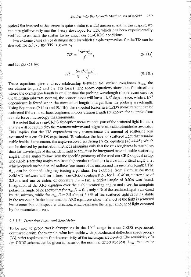
optical fiat inserted at the center, is quite similar to a TIS measurement. In this respect, wecan straightforwardly use the theory developed for TIS, which has been experimentallyverified, to estimate the scatter losses under our cm-CRDS conditions.
Two extreme cases can be distinguished for which simple expressions for the TIS can bederived: for ~R> 1 the TIS is given by:
16n2o2TIS = rms (9.lla)
and for ~/2<1 by:
TIS = 64n4u2~2 (9.llb)
These equations give a direct relationship between the surface roughness ~ thecorrelation length ~ and the TIS losses. The above equations show that for situationswhere the correlation length is smaller than the probing wavelength (the relevant case forthe thin filmlsubstrate system), the scatter losses will have a i/2~ dependence, while a 1it2dependence is found when the correlation length is larger than the probing wavelength.Using Equations (9.lla) and (9.llb), the expected losses in a CRDS measurement can beestimated if the rms surface roughness and correlation length are known, for example fromatomic force microscopy measurements.
It is noted that in a cm-CRDS absorption measurement, part of the scattered light from theanalyte will be captured by the resonator mirrors and might remain stable inside the resonator.This implies that the TIS expressions may overestimate the amount of scattering lossmeasured in a cm-CRDS experiment. To calculate the level of scattered light that remainsstable inside the resonator, the angle-resolved scattering (ARS) equation [43,44,45], whichcan be derived by perturbation methods assuming only that the rms roughness is much lessthan the wavelength of the incident light beam, must be integrated over all stable scatteringangles. These angles follow from the specific geometry of the used cm-CRDS optical setup.The stable scattering angles run from 0 (specular reflection) to a certain critical angle ~which depends on the size andradius ofcurvature of the mirrors and the resonatorlength 1. The°crit can be obtained using ray-tracing algorithms. For example, from a simulation usingZEMAX software and for a linear cm-CRDS configuration for 1=0.40 m, mirror size of2.5 cm, and mirror radius of curvature r = —1 m, a critical angle of 0.026 was found.Integration of the ARS equation over the stable scattering angles and over the completepolaroidal angle of 2n shows that for u,.,J~Z = 0.1, only 4 % of the scattered light is capturedby the mirrors, while for ~ 2.5 almost 30 % of the scattered light remains stablein the resonator. In the latter case the ARS equations show that most of the light is scatteredinto a cone about the specular direction, which explains the larger amount of light capturedby the resonator mirrors.
9.3.1.3 Detection Limit and Sensitivity
To be able to probe weak absorptions in the i07 range in a cm-CRDS experiment,comparable with, for example, what is possible with photothermal deflection spectroscopy[33], strict requirements for the sensitivity of the technique are needed. The sensitivity of acm-CRDS scheme can be given in terms of the minimal detectable loss, Lmjn, that can be
260 Cavity Ring-Down Spectroscopy: Techniques and Applications
expressed by the product of the roundtrip losses ~L1 and the relative uncertainty in thedetermination of the ring-down time:
Lmin = ~L1(co) x~ (9.12)
p Here, the uncertainty in the determination of the ring-down time is given in terms of thestandard deviation o-, of an ensemble of ring-down times, divided by the average ring-downtime. Equation (9.12) reveals the simplicity and challenge to obtain the highest sensitivityin a CRDS scheme: minimize the intrinsic loss and determine the ring-down time with thehighest possible precision. The roundtrip losses consist of mirror losses and losses related tothe analyte, usually an optical flat, such as absorption and scattering losses of the opticalflat. The mirror losses can be reduced to increase the reflectivity; however, too highreflectivity of the minors might reduce the signal output, thus decreasing the precision inthe determination of the ring-downtime. The absorption losses of the optical flat can usuallybe reduced to values lower than the mirror losses. For example, a fused silica optical flat canhave an OH contamination that gives rise to below-ppm absorption levels in the near-JR
It wavelength region. For standard polished optical flats, light scattering losses can be reducedto values around the ppm level at near-JR wavelengths. However, at visible wavelengths,scattering losses might be larger and may make a substantial contribution to the measured
losses. In general, within a carefully designed experiment the intrinsic losses are normallydetermined by the finite reflectivity of the mirrors e.g., L, 2 x 10 ~.
The relative uncertainty in the ring-down time is not significantly influenced by thepp insertion of the optical flat. Usually, a relative uncertainty of at least 1 % is achievable
for a CRDS experiment. Consequently, the minimal detectable loss is then found to be~2 x 10_6 per single laser shot. Averaging N laser shots further improves this number bya factor of 1/,JN.
r In the next section it will be shown that cm-CRDS schemes are indeed highly sensitiveand allow the measurement of weak absorptions in condensed media.
9.3.2 Measuring ex-situ Dangling Bonds in a-Si:H Films
P A schematic view of the setup which is used for measuring ex-situ dangling bonds in a-Si:Hfilms is shown in Figure 9.13. The experiments have been carried out with the tunable idleroutput of an optical parametric oscillator (OPO) which is pumped by the third harmonic ofa pulsed Nd:YAG laser operating at 30Hz. The idler output of the OPO can be tunedbetween photon energies of 0.6—1.8 eV and the resulting pulse has a typical bandwidth of10 cm’, a duration of 5 ns, and a pulse energy of 10 mJ. The pulse is injected into a stableoptical cavity formed by two planoconcave highly reflecting (R > 0.9997) dielectricminors without using mode-matching optics. The cavity is purged with dry nitrogen toreduce the effects of strong water absorptions. The decrease in light intensity inside thecavity was detected with a photomultiplier tube or a photodiode depending on the photonenergy used. As in Section 9.2, individual transients were sampled using a 12 bit, 100 MHz,data acquisition system and fitted with a standard weighted linear regression technique toextract the ring-down time. A typical result for two transients, one recorded with and onewithout an optical flat fused silica substrate inside the cavity, is shown in Figure 9.16.Reported values for cavity loss and absorptions were typically deduced from averages over400 individual ring-down times.
t

Studies into the Growth Mechanism of a-Si:H 261
c’i
53
C)(I)
Figure 9.17 shows the inherent loss of the cavity Lcat,j~~ as a function of the photon energy.To cover the complete photon energy shown, four sets of mirrors were used while severalparts of the spectrum could not be measured due to strong optical transitions of water lines.Also shown in Figure 9.17 are the losses Lsubstrate due to the quartz substrate onto which thea-Si:H films were deposited. L~b~trate was obtained from the losses Lcavity + Lsrubstrate,
measured with the substrate inside the cavity subtracted by the cavity losses Lcavj0. Of note
Photon energy E (eV)
Figure 9.17 Inherent optical loss of the empty cavity, Lcavjty and the optical loss induced bythe substrate, Lsubstrate, when placed inside the cavity (see inset). The sum of the two lossesLcavity + Lsubstrate defines the total intrinsic loss. Lcavity shows signatures of OH absorptions dueto strong optical transitions ofremaining water, while Lsubstrate shows absorption peaks related tovibrational modes of5104 and OH present in the substrate material (Reprinted with permissionfrom Aarts et a!., Direct and highly sensitive measurements of defect-related absorption inamorphous silicon thin films by cavity ringdown spectroscopy; AppI. Phys. Lett. 2004,84,3079.Copyright 2004, American Institute of Physics)
1000
100
10Resonator with optical flat:r= (7215+1-1) ns
0 10 20 30 40Time (ps)
Figure 9.16 Two single-exponential transients as recordedFigure 9.13
with the set-up shown in
1 02
0~ 10
53
5353o -4-J 10
—a— Lsubstrate
I • I
0.8 1.2 1.61 0~
262 Cavity Ring-Down Spectroscopy: Techniques and Applications
1 ~
i ~
~ 30) 10•0
0)o 2(2 100
a.~ 10(0.0
1002.0
Photon energy E (eV)
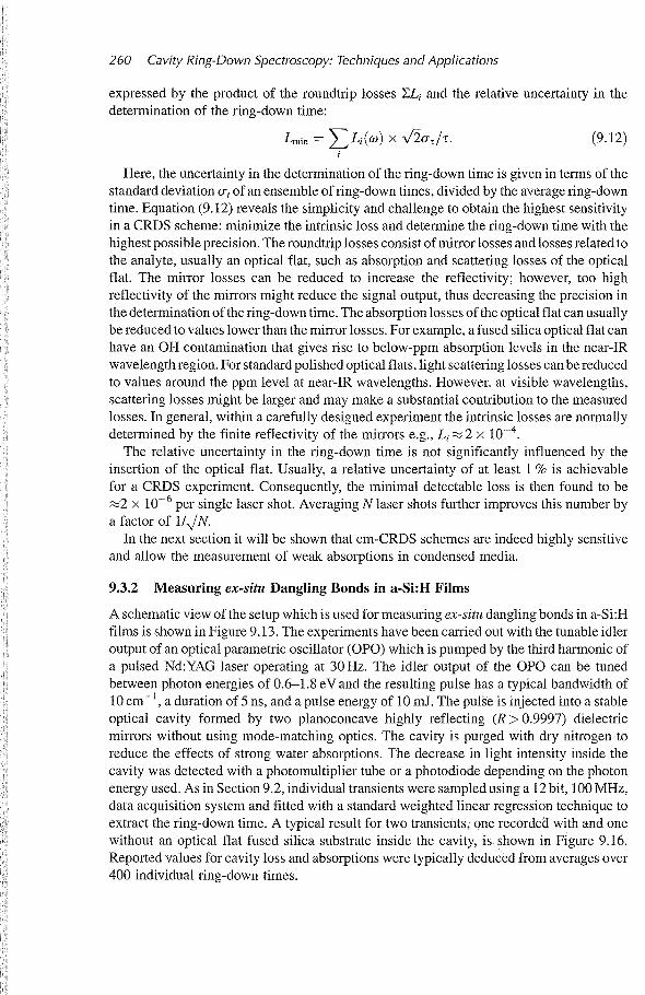
Figure 9.18 Absorption coefficientco ofa 1031 nm thick a-Si:H film as a function of the photonenergy as obtained by CRDS (L), photothermal deflection spectroscopy (0), and transmission-reflection spectroscopy (—). For CRDS, the absorption coefficient was determined from theoptical loss caused by the a-Si:H (inset) after a correction for interference in the film. Theabsolute scale of the PDS results was determined by linking the PDS data to the transmission-reflection data at a transmission value of 10 % (Reprinted with permission from Aarts et a!.,Direct and highly sensitive measurements of defect-related absorption in amorphous siliconthin films by cavity ringdown spectroscopy; Appi. Phys. Lett. 2004, 84, 3079. Copyright 2004,American Institute of Physics)
is the distinct peak around 1.0 eV in the absorption spectrum of the quartz, which reveals theabsorption due to the combined vibrational mode of the first overtone of the fundamentalOH and the tetrahedron vibration of SiO4 [46]. Using Ref. [46] the OH contamination in thequartz was estimated to be 150 ppm.
To establish the validity of the technique we measured the absorption coefficient of a1031-nm thick a-Si:H film deposited by an rf plasma at a substrate temperature of 250°Cand compared the result with the PDS technique. The absorption coefficient measured byPDS was obtained by the standard procedure and absolute values were deduced by linkingthe data to transmission—reflection (T—R) spectroscopy. The inset of Figure 9.18 depicts theloss LflI,,I due to the 1031—nm thin film as measured with CRDS. Clearly visible is a periodicmodulation of the loss as a function of the photon energy, which is caused by interferenceeffects in the film. Corrections for these interference effects were made using an ab initiomodel that determines the light intensity distribution in the a-Si:H film as a function ofthickness and wavelength. The resulting absorption coefficient of the 1031-nm thick film aswell as results obtained by PDS and T—R on the same sample are depicted in Figure 9.18. Itcan be observed that good agreement has been found between the CRDS and the PDStechnique and between CRDS and T—R.
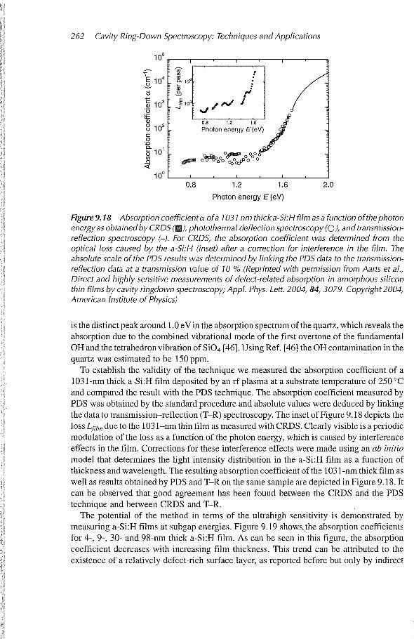
The potential of the method in terms of the ultrahigh sensitivity is demonstrated bymeasuring a-Si:H films at subgap energies. Figure 9.19 shows the absorption coefficientsfor 4-, 9-, 30- and 98-nm thick a-Si:H film. As can be seen in this figure, the absorptioncoefficient decreases with increasing film thickness. This trend can be attributed to theexistence of a relatively defect-rich surface layer, as reported before but only by indirect
I ~~I’IiHH[Iii; ~
0.8 1.2 1.6
Studies into the Growth Mechanism of a-Si:H 263
~10 —~
10~ 0.8 1.2 1.6
Photon energy E (eV)
Figure 9.19 Subgap absorption spectra showing the absorption coefficient (after interferencecorrections) for a-Si:H thin films with a thickness of 4 nm (n), 9 nm (0), 30 nm (A) and 98 nm(cy) (Reprinted with permission from Aarts et al., Direct and highly sensitive measurements ofdefect-related absorption in amorphous silicon thin films by cavity ringdown spectroscopy;AppI. Phys. Lett. 2004, 84, 3079. copyright 2004, American Institute of Physics)
techniques and not for such thin a-Si:H films [47,51]. The ability of CRDS to determine c~for such thin films, as well as the direct and absolute proof of a defect-rich surface layer,already indicates that CRDS is a very sensitive technique for defect spectroscopy. Anotherimportant observation in Figure 9.19 is that the absorption coefficient at subgap energiesdecreases much more rapidly at low energies for the 4-nm film than for the 98-nm film. It islikely that this spectral dissimilarity is caused by a different density of states, possiblycaused by a difference in the local environment of the defects and/or by a difference in thedefects probed [48]. In summary, we have proven that CRDS can be used for ultrasensitivedetection of defect-related absorptions in thin films with an ultimate sensitivity of 5 x 1 O_8and without the need for a calibration procedure. The absorption coefficient of a-Si:H filmsof thickness down to 4 nm was determined and reveals a distinct spectral dependence ascompared with thick films, thus illustrating the broad potential of the method.
9.4 Evanescent Wave CRDS on Dangling Bonds During a-Si:HFilm Growth
Photothermal deflection [49], constant photocurrent [50], electron spin resonance(ESR) [50], and cavity ring-down [51] spectroscopic techniques can be applied to DBdetection. Although constant photocurrent and photothermal deflection methods providethe required sensitivity, these techniques are not easily adapted to in-situ studies undergrowth conditions. ESR has been applied during growth and H-atom exposure of a-Si:Hfilms [50], although surface, bulk, and interface defects are not readily distinguished andthe set-up required an adaptation of the plasma set-up. By probing the sub-gap DB defectabsorption [49,50,52], cavity ring-down spectroscopy enables the determination of verylow absolute defect densities, as has been shown in the previous section. However, the
264 Cavity Ring-Down Spectroscopy: Techniques and Applications
conventional implementation of CRDS using a linear resonator is not adapted to in-situstudies of a-Si:H growth.
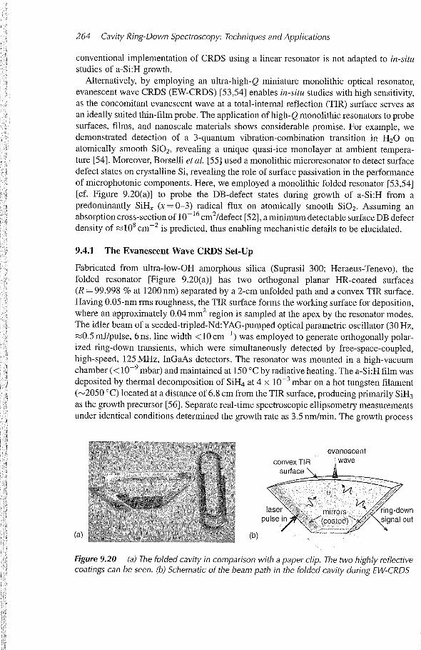
Alternatively, by employing an ultra-high-Q miniature monolithic optical resonator,evanescent wave CRDS (EW-CRDS) [53,54] enables in-situ studies with high sensitivity,as the concomitant evanescent wave at a total-internal reflection (TIR) surface serves asan ideally suited thin-film probe. The application of high-Q monolithic resonators to probesurfaces, films, and nanoscale materials shows considerable promise. For example, wedemonstrated detection of a 3-quantum vibration-combination transition in H20 onatomically smooth Si02, revealing a unique quasi-ice monolayer at ambient temperature [54]. Moreover, Borselli et al. [55] used a monolithic microresonator to detect surfacedefect states on crystalline Si, revealing the role of surface passivation in the performanceof microphotonic components. Here, we employed a monolithic folded resonator [53,54][cf. Figure 9.20(a)] to probe the DB-defect states during growth of a-Si:H from apredominantly SiHX (x 0—3) radical flux on atomically smooth 5i02. Assuming anabsorption cross-section of 10_16 cm2/defect [52], a minimum detectable surface DB defectdensity of 108 cm2 is predicted, thus enabling mechanistic details to be elucidated.
9.4.1 The Evanescent Wave CRDS Set-Up
Fabricated from ultra-low-OH amorphous silica (Suprasil 300; Heraeus-Tenevo), thefolded resonator [Figure 9.20(a)] has two orthogonal planar HR-coated surfaces(R 99.998 % at 1200 nm) separated by a 2-cm unfolded path and a convex TIR surface.Having 0.05-nm rms roughness, the TIR surface forms the working surface for deposition,where an approximately 0.04 mm2 region is sampled at the apex by the resonator modes.The idler beam of a seeded-tripled-Nd:YAG-pumped optical parametric oscillator (30 Hz,n~0.5 mJ!pulse, 6 ns, line width <10 cm1) was employed to generate orthogonally polarized ring-down transients, which were simultaneously detected by free-space-coupled,high-speed, 125 MHz, InGaAs detectors. The resonator was mounted in a high-vacuumchamber (<i0~ mbar) and maintained at 150°C by radiative heating. The a-Si:H film wasdeposited by thermal decomposition of SiH4 at 4 x i0~ mbar on a hot tungsten filament(‘-~2050 °C) located at a distance of 6.8 cm from the TIR surface, producing primarily SiH3as the growth precursor [56]. Separate real-time spectroscopic ellipsometry measurementsunder identical conditions determined the growth rate as 3.5 nm/mm. The growth process
(a) (b)
Figure 9.20 (a) The folded cavity in comparison with a paper clip. The two highly reflectivecoatings can be seen. (b) Schematic of the beam path in the folded cavity during EW-CRDS
evanescentconvex TIR wave
Studies into the Growth Mechanism of a-Si:H 265
was studied by performing many growth cycles (flux-onlgrowthlflux-off), resulting in afinal thickness of 800 nm.
9.4.2 Measuring Dangling Bonds During a-Si:H Film Growth
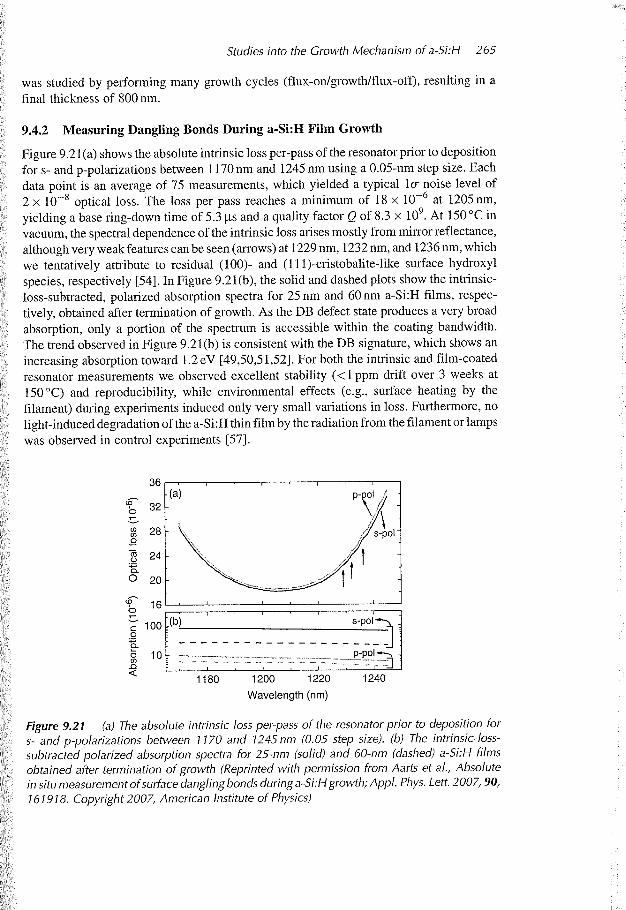
Figure 9.21(a) shows the absolute intrinsic loss per-pass of the resonator prior to depositionfor s- and p-polarizations between 1170 nm and 1245 nm using a 0.05-nm step size. Eachdata point is an average of 75 measurements, which yielded a typical 10- noise level of2 x 10~8 optical loss. The loss per pass reaches a minimum of 18 x 10~6 at 1205 nm,yielding a base ring-down time of 5.3 ~ts and a quality factor Q of 8.3 x ~ At 150°C invacuum, the spectral dependence of the intrinsic loss arises mostly from mirror reflectance,although very weak features can be seen (arrows) at 1229 nm, 1232 nm, and 1236 nm, whichwe tentatively attribute to residual (100)- and (11 1)-cristobalite-like surface hydroxylspecies, respectively [54]. In Figure 9.2 1(b), the solid and dashed plots show the intrinsic-loss-subtracted, polarized absorption spectra for 25 nm and 60 nm a-Si:H films, respectively, obtained after termination of growth. As the DB defect state produces a very broadabsorption, only a portion of the spectrum is accessible within the coating bandwidth.The trend observed in Figure 9.21(b) is consistent with the DB signature, which shows anincreasing absorption toward 1.2eV [49,50,51,52]. For both the intrinsic and film-coatedresonator measurements we observed excellent stability (<1 ppm drift over 3 weeks at150°C) and reproducibility, while environmental effects (e.g., surface heating by thefilament) during experiments induced only very small variations in loss. Furthermore, nolight-induced degradation of the a-Si:H thin film by the radiation from the filament or lampswas observed in control experiments [57].
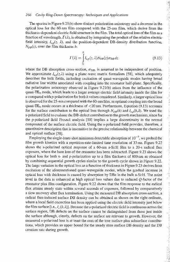
36(a)
~32
g~ 280
~ 240.o 20
16 ________________________________________________________
.~ (b) s~poI—~
8 10I I I I
1180 1200 1220 1240
Wavelength (nm)
Figure 9.21 (a) The absolute intrinsic loss per-pass of the resonator prior to deposition fors- and p-polarizations between 1170 and 1245 nm (0.05 step size). (b) The intrinsic-loss-subtracted polarized absorption spectra for 25-nm (solid) and 60-nm (dashed) a-Si:H filmsobtained after termination of growth (Reprinted with permission from Aarts et a!., Absolutein situ measurement ofsurface dangling bonds during a-Si:H growth; App!. Phys. Lett. 2007, 90,161918. Copyright 2007, American Institute of Physics)
266 Cavity Ring-Down Spectroscopy: Techniques and Applications
[ The spectra in Figure 9.21(b) show distinct polarization anisotropy and a decrease in theoptical loss for the 60-nm film compared with the 25-nm film, which derive from thethickness-dependent electric field structure in the film. The total optical loss of the film as afunction of wavelength, 1(A), is obtained by integrating the product of the relative electricfield intensity, I~~(z. 2). and the position-dependent DB-density distribution function,NDB(Z), over the film thickness h:
h
1(2) = JISP(z~2)NDB(z)~DBdz (9.13)
where the DB absorption cross-section, 0~DB’ is assumed to be independent of position.We approximate I~~(z,A) using a plane-wave matrix formalism [58], which adequatelydescribes the bulk fields, including excitation of quasi-waveguide modes having broadradiative line widths associated with coupling into the resonator half-plane. Specifically,the polarization anisotropy observed in Figure 9.21(b) arises from the influence of thequasi-TE0 mode, which leads to a larger average electric field intensity inside the film fors-compared with p-polarization for both h values considered. Similarly, a larger optical lossis observed for the 25-nm compared with the 60-nm film, as optimal coupling into the broadquasi-TE0 mode occurs at a thickness of <20 nm. Furthermore, Equation (9.13) accountsfor the surface contribution to the optical loss through NDB(h) and I~~(h,2). We used thes-polarized field to evaluate the DB-defect contribution to the growth mechanism, since forthe p-polarized field Fresnel analysis [58] implies a large discontinuity in the normalcomponent of the surface electric field. Using the s-polarized field provides, therefore, aquantitative description that is insensitive to the precise relationship between the chemicaland optical surface [58].
Employing the single-laser-shot minimum detectable absorption of 10~, we probed thefilm growth kinetics with a repetition-rate-limited time resolution of 33 ms. Figure 9.22shows the s-polarized optical response of a 60-nm a-Si:H film to a 20-s radical fluxexposure, where the base loss of the resonator has been subtracted. Figure 9.23 shows theoptical loss for both s- and p-polarization up to a film thickness of 800 nm as obtainedby combining sequential growth cycles similar to the growth cycle shown in Figure 9.22.The large variation in the optical loss as a function of thickness in Figure 9.23 derives fromexcitation of the aforementioned quasi-waveguide modes, while the gradual increase inoptical loss with thickness is caused by absorption by DBs in the bulk a-Si:H. The noiselevel in the data is enhanced at high optical loss values due to reduced Q-factor of theresonator plus film configuration. Figure 9.22 shows that the film response to the radicalflux attains steady state within several seconds of exposure, followed by comparativelya slow recovery after flux termination. Using the measured DB absorption cross-section, aradical flux-induced surface DB density can be obtained as shown on the right ordinate,where a local field correction has been applied using the electric field intensity just belowthe film surface [i.e., I~ (h,2)]. Because the s-polarized electric field is continuous across thesurface region, DB defects on the surface cannot be distinguished from those just insidethe surface although, clearly, defects on the surface are relevant to growth. However, themeasured s-polarized loss is at least the sum of the true surface plus subsurface contributions, which provides an upper bound for the steady state surface DB density and the DBcreation rate during growth.
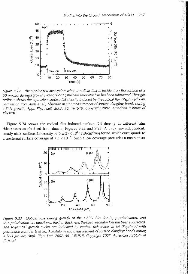
Studies into the Growth Mechanism of a-Si:H 267
30 40 50 60 70 80Time (s)
Figure 9.22 The s-polarized absorption when a radical flux is incident on the surface of a60-nm film during a growth cycle ofa-Si:H; the base resonator loss has been subtracted. The rightordinate shows the equivalent surface DB density induced by the radical flux (Reprinted withpermission from Aarts et al., Absolute in situ measurement of surface dangling bonds duringa-Si:H growth; AppI. Phys. Lett. 2007, 90, 161918. copyright 2007, American Institute ofPhysics)
Figure 9.24 shows the radical flux-induced surface DB density at different filmthicknesses as obtained from data in Figures 9.22 and 9.23. A thickness-independent,steady-state, surface DB density of(5 ± 2) x 101~ DB/cm2 was found, which corresponds toa fractional surface coverage of ~5 x i0~. Such a low coverage precludes a mechanism
Figure 9.23 Optical loss during growth of the a-Si:H film for (a) p-polarization, and(b) s-polarization as a function of the film thickness; the base resonator loss has been subtracted.The sequential growth cycles are indicated by vertical tick marks in (a) (Reprinted withpermission from Aarts et al., Absolute in situ measurement of surface dangling bonds duringa-Si:H growth; Appl. Phys. Lett. 2007, 90, 161918. copyright 2007, American Instilute ofPhysics)
50
45
~D 400
~35Cl)0
—J 30ccC)
~250
20
6
00 10 20
20
10
IIIII~III I 111111111 I II I
(a) p-pci
I ~
j ~ _~ ~ \ _,
._~___—( ~ ~ I — I
C
U)Cl)0
*30
0 200 400 600Thickness (nm)
800

268 Cavity Ring-Down Spectroscopy: Techniques and Applications
I 10~
-o----_~_E10 10 ~
103~~f ~ ciI0 50 100 150 200 250 300 350 400
Thickness (nm)
Figure 9.24 The experimental DB surface density induced by the radical flux (left ordinate) andthe corresponding DB creation rate (right ordinate, solid line) fora range of film thicknesses. TheDB creation rate is contrasted with the calculated value (dashed line) needed to account forthe actual growth rate based on a ‘dangling bond’ dependent growth mechanism (Reprintedwith permission from Aarts et al., Absolute in situ measurement of surface dangling bondsduring a-Si:H growth; AppI. Phys. Lett. 2007, 90, 161918. Copyright 2007, American Instituteof Physics)
based on direct precursor-defect binding, as a coverage of ~0. 1 is required to account fortypical a-Si:H growth rates, assuming a sticking probability for radical-radical coupling of0.1 [51]. However, a low surface coverage does not eliminate mechanisms involving surfacediffusion of weakly bound precursors [26,27] or a direct insertion mechanism [59,60]. Yetthe role of the DB is significantly different for these latter two mechanisms. For precursor-mediated growth, the creation rate of DB defects is critical and must at least equal thegrowth rate (DB passivation rate), while for direct insertion the DB defect is not specificallyrelevant. As also shown in Figure 9.24, the initial DB creation rate, which was obtained frommany growth cycles at various film thicknesses, is found to be (5 ±3) x 1012 DB/cm2 s.Comparing this value with the actual growth rate of 2.9 x 10¹⁴ Si/cm2 s, assuming a Sidensity of 5 x 1022 cm3 in a-Si:H, the DB creation rate is 60 times too small to account forthe actual growth rate.
Acknowledgements
We thank Peter van den Oever, Maarten Boogaarts, Arno Smets, Alquin Stevens, Jean-Pierrevan Helden, Karine Letourneur, Yolanda Barrel, Mariadriana Creatore, Andrew Pipino, andDaan Schram for their contributions to the work on which this chapter is based. The authorsacknowledge the Technical Laboratory Automation group of the Eindhoven Universityof Technology and the technical assistance by M.J.F. van de Sande, J.F.C. Jansen, H.M.M.de Jong. J. Zeebregts and A.B.M. Hüsken. This research was supported by The Netherlands
Studies into the Growth Mechanism of a-Si:H 269
Foundation for Fundamental Research on Matter (FOM) and the Royal NetherlandsAcademy of Sciences and Arts (KNAW) by the fellowship of one of the authors (W.K.).
References
[1] Ohring, M., The Materials Science of Thin Films, Academic Press: San Diego, USA, 1992.[2] Crowell, J.E. Chemical methods of thin film deposition: Chemical vapor deposition, atomic
layer deposition, and related technologies, J. Vac. Sci. Technol. 2003, A 21, S88.[3] Rossnagel, SM. Thin film deposition with physical vapor deposition and related technologies,
J. Vac. Sci. Technol. 2003, A 21, S74.[4] Venables, J.A.; Spiller, G.D.T.; Hanbücken, M. Nucleation and growth of thin films, Rep. Prog.
Phys. 1984, 47, 399.[5] Mertens, H.; Polman, A.; Aarts, I.M.P.; Kessels, W.M.M.; van de Sanden, M.C.M. Absence of
the enhanced intra-4f transition cross section at 1.5 urn of Er3 + in Si-rich Si02, AppI. Phys. Lett.2005, 86, 241109.
[6] See e.g., Kessels, W.M.M.; van de Sanden, M.C.M.; Severens, R.J.; Schram, D.C. Surfacereaction probability during fast deposition of hydrogenated amorphous silicon with a remotesilane plasma, J. Appl. Phys. 2000, 87, 3313 and references therein.
[7] McCurdy, P.R.; Bogart, K.H.A.; Dalleska, N.F.; Fisher, ER. A modified molecular beaminstrument for the imaging of radicals interacting with surfaces during plasma processing, Rev.Sci. Instrum. 1997, 68, 1684.
[8] Perrin, J.; Shiratani, M.; Kae-Nune, P.; Videlot, H.; Jolly, J.; Guillon, J. Surface reactionprobabilities and kinetics of H, SiH3, Si2H5, CH3, and C2H5 during deposition of a-Si:H and a-C:H from H2, SiH4, and CH4 discharges, J. Vac. Sci. Technol. 1998, A 16, 278.
[9] Kae-Nune, P.; Perrin, J.; Guillon, J.; Jolly, J. Mass spectrometry detection of radicals in SiH4-CH4-H2 glow discharge plasmas, Plasma Sources Sci. Technol. 1995, 4, 250.
[10] Atkinson, D.B.; Hudgens, J.W. Chemical Kinetic Studies Using Ultraviolet Cavity Ring-DownSpectroscopic Detection: Self-Reaction of Ethyl and Ethylperoxy Radicals and the Reaction02 + C2H5 —* C2H502, .1. Phys. Chem. A 1997, 101, 3901 and references therein.
[11] Yalin, A.P.; Zare, R.N.; Laux, CO.; Kruger, C.H. Temporally resolved cavity ring-downspectroscopy in a pulsed nitrogen plasma, AppI. Phys. Lett. 2002, 81, 1408.
[12] Hoefnagels, J.P.M.; Stevens, A.A.E.; Boogaarts, M.G.H.; Kessels, W.M.M.; van de Sanden,M.C.M. Time-resolved cavity ring-down spectroscopic study of the gas phase and surfaceloss rate of Si and SiH3 plasma radicals, Chem. Phys. Lett. 2002, 360, 189.
[13] Kessels, W.M.M.; Leewis, C.M.; van de Sanden, M.C.M.; Schram, D.C. Formation of cationicsilicon clusters in a remote silane plasma and their contribution to hydrogenated amorphoussilicon film growth, J. AppI. Phys. 1999, 86, 4029.
[14] Baklanov, A.V.; Krasnoperov, L.N. UVAbsorption spectrum and rate constant for self-reactionof silyl radicals, J. Phys. Chem. 2001, 105, 4917.
[15] Lightfoot, P.D.; Becerra, R.; Jemi-Alade, A.A.; Lesclaux, R. The UV absorption spectrum ofSiH3, Chem. Phys. Lett. 1991, 180, 441.
[16] Radzig, A.A.; Srnirnov, B.M. References Data on Atoms, Molecules and Ions, Springer-Verlag:Berlin-Heidelberg, 1985.
[17] Luque, J.; Crosley, DR.; LIFBASE: Database and Spectral Simulation Program(Version 1.5),SRI International Report MP 99-009 1999.
[18] Kessels, W.M.M.; Hoefnagels, J.P.M.; Boogaarts, M.G.H.; Schram, D.C.; van de Sanden, M.C.M. Cavity ring down study of the densities and kinetics of Si and SiH in a remote Ar-H2-SiH4plasma, J. Appl. Phys. 2001, 89, 2065.
[19] Courteille, C.; Dorier, J.-L.; Hollenstein, Ch.; Sansonnens, L.; Howling, A.A. Partial-depthmodulation study of anions and neutrals in low-pressure silane plasmas, Plasma Sources Sci.Technol. 1996, 5, 210.
[20] Technical Laboratory Automation Group, Eindhoven University of Technology, Den Dolech 2,5600 MB Eindhoven, The Netherlands.
270 Cavity Ring-Down Spectroscopy: Techniques and Applications
[211 Kessels, W.M.M.; Houston, I.J.; Nadir, K.; van de Sanden, M.C.M. High-rate deposition ofnanocrystalline silicon using the expanding thermal plasma technique, J. Non-Cryst. Solids2006, 352, 915.
[221 Chantry, P.J. A simple formula for diffusion calculations involving wall reflection and lowdensity, J. AppI. Phys. 1987, 62, 1141.
[23] Perrin, J.; Leroy, 0.; Bordage, M.C. Cross-sections, rate constants and transport coefficients insilane plasma chemistry, C’ontrib. Plasma. Phys. 1996, 36, 3.
[24] van de Sanden, M.C.M.; Severens, R.J.; Kessels, W.M.M.; Meulenbroeks, R.F.G.; Schram, D.C.Plasma chemistry aspects of a-Si:H deposition using an expanding thermal plasma, J. Appi.Phys. 1998, 84, 2426.
[25] Kessels, W.M.M.; Hoefnagels, J.P.M.; van de Oever, P.J.; Barrel, Y.; van de Sanden, M.C.M.Temperature dependence of the surface reactivity of SiH3 radicals and the surface silicon hydridecomposition during amorphous silicon growth, Surf Sci. Lett. 2003, 547, L865.
[26] Ganguly, G.; Matsuda, A. Defect formation during growth of hydrogenated amorphous silicon,Phys. Rev. B 1993, 47, 3661.
[27] Kessels, W.M.M.; Smets, A.H.M.; Marra, D.C.; Aydil, ES.; Schram, D.C.; van de Sanden,M.C.M. On the growth mechanism of a-Si:H, Thin Solid Films 2001, 383, 154.
[28] Gates, S.M.; Kulkarni, S.K. Kinetics of surface reactions in very low-pressure chemical vapordeposition of Si from SiH4, Appl. Phys. Lett. 1991, 58, 2963.
[29] Toyoshima, Y.; Arai, K.; Matsuda, A.; Tanaka, K. In situ characterization of the growing a-Si:Hsurface by JR spectroscopy, J. Non-Cryst. Solids 1991, 137, 765.
[30] Umeda, T.; Yamasaki, S.; Isoya, J.; and Tanaka, K. Electron-spin-resonance center of danglingbonds in undoped a-Si:H, Phys. Rev. B 1999, 59, 4849.
[31] Zangwill, A. Physics at Surfaces, Cambridge University press: Cambridge, 1988.[32] Street, R.A. Hydrogenated amorphous silicon, Cambridge University Press: Cambridge, 2002.[33] Jackson, W.B.; Amer, N.M.; Boccara, AC.; : Fournier, D. Photothermal deflection spectroscopy
and detection, Appi. Optics 1981, 20, 1333.[34] Vamiëek, M.; Koãka, J.; Poruba, A.; Fejfar, A. Direct measurement of the deep defect density in
thin amorphous silicon films with the ‘absolute’ constant photocurrent method, J. AppI. Phys.1995, 78, 6203.
[35] Das, U.K.; Yasuda, T.; Yamasaki, S. Fast Diffusion of H and creation of dangling bonds inhydrogenated amorphous silicon studied by in situ ESR, Phys. Rev. Lett. 2000, 85, 2324.
[36] Engeln, R.; Berden, G.; van den Berg, E.; Meijer, G. Polarization dependent cavity ring downspectroscopy, J. Chem. Phys. 1997, 107, 4458.
[37] Engeln, R.; von Helden, G.; van Roij, A.J.A.; Meijer, G. Cavity ringdown spectroscopy on solidC60, J. Chem. Phys. 1999, 110, 2732.
[38] Marcus, GA.; Schwettman, HA. Cavity ringdown spectroscopy of thin films in the midinfrared, AppI. Optics 2002, 41, 5167.
[39] Kieine, D.; Lauterbach, J.; Kleinermanns, K.; Hering, P. Cavity ring-down spectroscopy ofmolecularly thin iodine layers, Appi. Phys. B 2001, 72, 249.
[40] Gerrard, A.; Burch, J.M. Introduction to Matrix Methods in Optics, John Wiley & Sons: London,1975.
[41] Lehmann, K.K.; Romanini, D. The superposition principle and cavity ringdown spectroscopy,.1. Chem. Phys. 1996, 105, 10263.
[42] Terasaki, A.; Kondow, T. Continuous-wave cavity ringdown spectroscopy applied to solids:properties of a Fabry—Perot cavity containing a transparent substrate, J. Opt. Soc. Am. B 2005,22, 675.
[43] Beckmann, P.; Spizzichino, A. The Scattering ofElectromagnetic Wavesfrom Rough Surfaces,Pergamon: New York, 1963.
[44] Elson, J.M. Light scattering from semi-infinite media for non-normal incidence, Phys. Rev. B1975, 12, 2541.
[45] Elson, J.M.; Rahn, J.P.; Bennett, J.M. Relationship of the total integrated scattering frommultilayer-coated optics to angle of incidence, polarization, correlation length, and roughnesscross-correlation properties, Appl. Optics. 1983, 22, 3207.
Studies into the Growth Mechanism of a-Si:H 271
[461 Logunov, S.L. Cavity ringdown detection of losses in thin films in the telecommunicationwavelength window, Appi. Optics 2001, 40, 1570.
[471 Wheeler, M.D.; Newman, S.M.; Off-Ewing, A.J.; Ashfold, M.N.R. Cavity ring-down spectroscopy, J. Chem. Soc., Faraday Trans. 1998, 94, 337.
[48] Beckman, P.; Spizzichino, A. The Scattering of Electromagnetic Waves from Rough Sutfaces,Pergamon Press: Oxford, 1963.
[49] Jackson, W.B.; Biegelsen, D.K.; Nemanich, R.J.; Knights, J.C. Optical absorption spectra ofsurface or interface states in hydrogenated amorphous silicon, Appi. Phys. Lett. 1983, 42, 105.
[50] Yamasaki, S.; Umeda, T.; Isoya, J.; Tanaka, K. In situ electron-spin-resonance measurements offilm growth of hydrogenated amorphous silicon, App!. Phys. Lett. 1997, 70, 1137.
[51] Aarts, I.M.P.; Hoex, B.; Smets, A.H.M.; Engeln, R.; Kessels, W.M.M.; van de Sanden, M.C.M.Direct and highly-sensitive measurement of defect-related absorption in amorphous silicon thinfilms by cavity ringdown spectroscopy, App!. Phys. Lett. 2004, 84, 3079.
[52] Wyrsch, N.; Finger, F.; Mcmahon, T.J.; Vanecek, M. How to reach more precise interpretation ofsubgap absorption spectra in terms of deep defect density in a-Si:H, J. Non-Cryst. Solids 1991,137, 347.
[53] Aarts, I.M.P.; Pipino, A.C.R.; Hoefnagels, J.P.M.; Kessels, W.M.M.; van de Sanden, M.C.M.Quasi-Ice monolayer on atomically smooth amorphous Si02 at room temperature observed witha high-finesse optical resonator, Phys. Rev. Lett. 2005, 95, 166104.
[54] Pipino, A.C.R. Ultrasensitive surface spectroscopy with a miniature optical resonator, Phys. Rev.Lett. 1999, 83, 3093.
[55] Borselli, M.; Johnson, T.J.; Painter, 0. Measuring the role of surface chemistry in siliconmicrophotonics, App!. Phys. Lett. 2006, 88, 131.
[56] Molenbroek, B.C.; Mahan, A.H.; Gallagher, A. Mechanisms influencing ‘hot-wire’ depositionof hydrogenated amorphous silicon, J. App!. Phys. 1997, 82, 1909.
[57] Staebler, DL.; Wronski, CR. Reversible conductivity changes in discharge-produced amorphous Si, App!. Phys. Lett. 1977, 31, 292.
[58] Ohta, K.; Ishida, H. Matrix formalism for calculation of electric field intensity of light instratified multilayered films, App!. Opt. 1990, 29, 1952.
[59] von Keudell, A.; Abelson, J.R. Direct insertion of SiH3 radicals into strained Si—Si surfacebonds during plasma deposition of hydrogenated amorphous silicon films, Phys. Rev. B 1999,59,5791.
[60] Agarwal, S.; Valipa, M.S.; Hoex, B.; van de Sanden, M.C.M.; Maroudas, D.; Aydil, E.S.Interaction of SiH3 radicals with an amorphous deuterated (hydrogenated) silicon surface, SuifSci. 2005, 598, 35.