risc vs cisc
TRANSCRIPT
RISC versus CISC: A Tale of Two Chips
Dileep BhandarkarIntel Corporation
Santa Clara, California, USA
AbstractThis paper compares an aggressive RISC and CISCimplementation built with comparable technology.The two chips are the Alpha* 21164 and the IntelPentium Pro processor. The paper presentsperformance comparisons for industry standardbenchmarks and uses performance counter statisticsto compare various aspects of both designs.
IntroductionIn 1991, Bhandarkar and Clark published a papercomparing an example implementation from the RISCand CISC architectural schools (a MIPS* M/2000 and aDigital VAX* 8700) on nine of the ten SPEC89benchmarks. The organizational similarity of thesemachines provided an opportunity to examine thepurely architectural advantages of RISC. That papershowed that the resulting advantage in cycles perprogram ranged from slightly under a factor of 2 toalmost a factor of 4, with a geometric mean of 2.7. Thispaper attempts yet another comparison of a leadingRISC and CISC implementation, but using chipsdesigned with comparable semiconductor technology.The RISC chip chosen for this study is the DigitalAlpha 21164 [Edmondson95]. The CISC chip is theIntel Pentium Pro processor [Colwell95]. The resultsshould not be used to draw sweeping conclusions aboutRISC and CISC in general. They should be viewed as asnapshot in time. Note that performance is alsodetermined by the system platform and compiler used.
Chip Overview
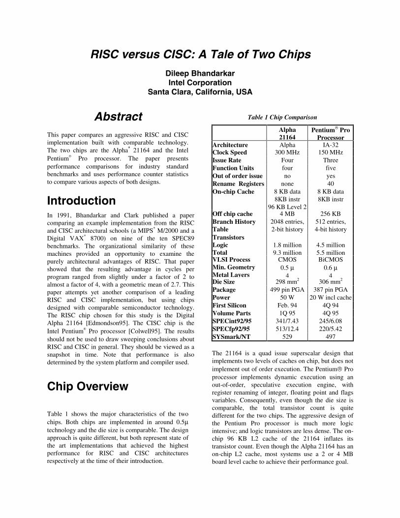
Table 1 shows the major characteristics of the twochips. Both chips are implemented in around 0.5µtechnology and the die size is comparable. The designapproach is quite different, but both represent state ofthe art implementations that achieved the highestperformance for RISC and CISC architecturesrespectively at the time of their introduction.
Table 1 Chip Comparison
Alpha21164
Pentium ProProcessor
Architecture Alpha IA-32Clock Speed 300 MHz 150 MHzIssue Rate Four ThreeFunction Units four fiveOut of order issue no yesRename Registers none 40On-chip Cache 8 KB data
8KB instr96 KB Level 2
8 KB data8KB instr
Off chip cache 4 MB 256 KBBranch HistoryTable
2048 entries,2-bit history
512 entries,4-bit history
TransistorsLogicTotal
1.8 million9.3 million
4.5 million5.5 million
VLSI ProcessMin. GeometryMetal Layers
CMOS0.5 µ
4
BiCMOS0.6 µ
4Die Size 298 mm2 306 mm2
Package 499 pin PGA 387 pin PGAPower 50 W 20 W incl cacheFirst Silicon Feb. 94 4Q 94Volume Parts 1Q 95 4Q 95SPECint92/95 341/7.43 245/6.08SPECfp92/95 513/12.4 220/5.42SYSmark/NT 529 497
The 21164 is a quad issue superscalar design thatimplements two levels of caches on chip, but does notimplement out of order execution. The Pentium Proprocessor implements dynamic execution using anout-of-order, speculative execution engine, withregister renaming of integer, floating point and flagsvariables. Consequently, even though the die size iscomparable, the total transistor count is quitedifferent for the two chips. The aggressive design ofthe Pentium Pro processor is much more logicintensive; and logic transistors are less dense. The on-chip 96 KB L2 cache of the 21164 inflates itstransistor count. Even though the Alpha 21164 has anon-chip L2 cache, most systems use a 2 or 4 MBboard level cache to achieve their performance goal.

.
Alpha 21164
The Alpha 21164 microprocessor consists of fiveindependent functional units as shown in Figure 1:
• Instruction fetch and decode unit (Ibox), whichincludes:
Instruction prefetcher and instructiondecoder
Branch prediction Instruction translation buffer
Interrupt support• Integer execution unit (Ebox)• Floating-point execution unit (Fbox)• Memory address translation unit (Mbox), which
includes: Data translation buffer (DTB) Miss address file (MAF) Write buffer
• Cache control and bus interface unit (Cbox) with
external interface
Instruction Cache (ICACHE)
BranchHistory Table TAG DATA
IntegerExecution Unit
(EBOX)
Multliplier
Adder
ShifterLogic Box
Floating-PointExecution Unit
(FBOX)
InstructionFetch/Decode Unit
(IBOX)
Prefetcher
InstructionBuffer
InstructionSlotter
BranchPrediction
Multiplier
Divider
Integer Register File (IRF) Floating-Point Register File (FRF)
Memory Address Translation Unit (MBOX)
DcacheAccess Control
Miss AddressFile
Write Buffer Dual-ReadTransaction Buffer
Data Cache (DCACHE)
TAG DATA
Adder
Instruction
Issuer
Adder
Logic Box
Branch/Jump
Cache Control and Bus Interface Unit (CBOX)
ScacheAccessControl
ExternalBcacheControl
BusInterfaceUnit (BIU)
SROMInterface Clocks
I/O ControlBcache TagBcache ControlDataAddress
ScacheSet 1 Set 2 Set 3
Tag Data Tag Data Tag Data
Interrupts
Clock
Reference Clock
System Clock
Figure 1 Alpha 21164 Block Diagram
It also includes three on-chip caches; an instructioncache, a data cache, and a second-level cache. Theinstruction unit fetches, decodes, and issuesinstructions to the integer unit, memory managementunit, and floating point unit. It manages the pipelines,the program counter, the instruction cache,prefetching, and I-stream memory management. It candecode up to 4 instructions in parallel and check thatthe required resources are available for each.
The integer execution unit contains two 64-bit integerpipelines. Results of most integer operations areavailable for use by the subsequent instruction. The
integer unit also partially executes all memoryinstructions by calculating the effective address.
The memory management unit processes all load andstore instructions. Two loads can be executed inparallel due to the dual-ported data cache. Up to 24load instructions can be in progress at any time. Thememory management unit also manages the datacache and logic that serializes and merges loadinstructions that miss the data cache.
The cache control and bus interface unit processes allaccesses sent by the memory management unit andimplements all memory related external interfacefunctions. It controls the second level cache and
.
manages the external backup cache. Its 40 bitphysical address supports 1 terabyte of physicaladdress space.
The floating point unit contains a floating pointmultiply pipeline and a floating point add pipeline.Divides are associated with the add pipeline but arenot pipelined themselves.
The instruction cache (Icache) is an 8KB directmapped, virtually indexed physical cache. The datacache (Dcache) is a dual ported, 8KB write through,read allocate, direct mapped, virtually indexedphysically addresssed cache with 32-byte blocks. Theaccess time is 2 cycles and the bandwidth is 16 bytesper cycle. The on-chip second level cache (Scache) isa 96KB, 3-way set associative, physical, write back,write allocate, combined data and instruction cache. Itis fully pipelined and supports both 32-byte and 64-byte blocks. Access time is 6 cycles after I or D cachemiss, and bandwidth is 16 bytes per cycle.
The 21164 supports and fully manages an optionaldirect mapped external backup cache (Bcache). Thiscache is a physical, write back, write allocate cachewith 32-byte or 64-byte blocks. The backup cachecontroller supports wave pipelining in the 64-byte
mode. It is a mixed data and instruction cache. Thesystem designer can select a Bcache size of 1, 2, 4, 8,16, 32, or 64 megabytes. The minimum latency is 4cycles and a maximum rate of 16 bytes every 4cycles.
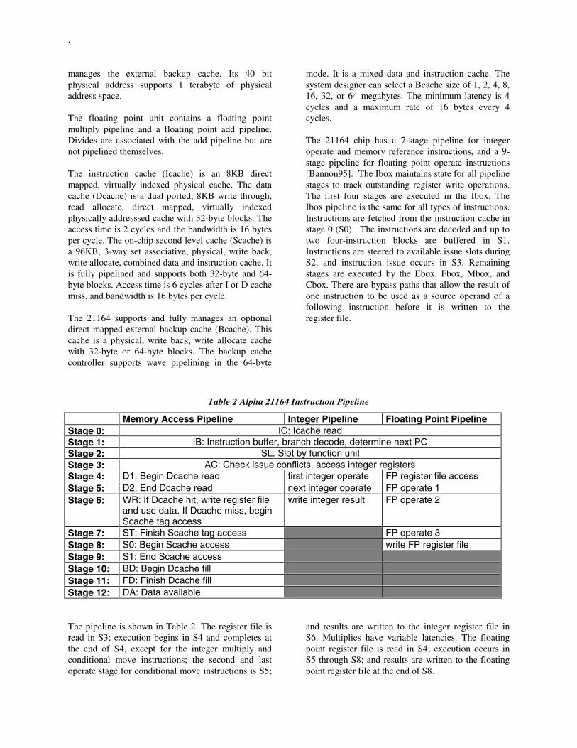
The 21164 chip has a 7-stage pipeline for integeroperate and memory reference instructions, and a 9-stage pipeline for floating point operate instructions[Bannon95]. The Ibox maintains state for all pipelinestages to track outstanding register write operations.The first four stages are executed in the Ibox. TheIbox pipeline is the same for all types of instructions.Instructions are fetched from the instruction cache instage 0 (S0). The instructions are decoded and up totwo four-instruction blocks are buffered in S1.Instructions are steered to available issue slots duringS2, and instruction issue occurs in S3. Remainingstages are executed by the Ebox, Fbox, Mbox, andCbox. There are bypass paths that allow the result ofone instruction to be used as a source operand of afollowing instruction before it is written to theregister file.
Table 2 Alpha 21164 Instruction Pipeline
Memory Access Pipeline Integer Pipeline Floating Point PipelineStage 0: IC: Icache readStage 1: IB: Instruction buffer, branch decode, determine next PCStage 2: SL: Slot by function unitStage 3: AC: Check issue conflicts, access integer registersStage 4: D1: Begin Dcache read first integer operate FP register file accessStage 5: D2: End Dcache read next integer operate FP operate 1Stage 6: WR: If Dcache hit, write register file
and use data. If Dcache miss, beginScache tag access
write integer result FP operate 2
Stage 7: ST: Finish Scache tag access FP operate 3Stage 8: S0: Begin Scache access write FP register fileStage 9: S1: End Scache accessStage 10: BD: Begin Dcache fillStage 11: FD: Finish Dcache fillStage 12: DA: Data available
The pipeline is shown in Table 2. The register file isread in S3; execution begins in S4 and completes atthe end of S4, except for the integer multiply andconditional move instructions; the second and lastoperate stage for conditional move instructions is S5;
and results are written to the integer register file inS6. Multiplies have variable latencies. The floatingpoint register file is read in S4; execution occurs inS5 through S8; and results are written to the floatingpoint register file at the end of S8.
.
Virtual address calculation occurs and data cacheaccess begins in S4; data cache access completes,address translation occurs, and cache hit is calculatedin S5. If the access hits, the data is written to theregister file (load case) or the cache (store case) inS6. The pipeline continues in the case of a data cachemiss as follows: second-level cache access begins inS6 and ends in S9; the data cache fill begins in S10;the integer register file write occurs and the datacache fill completes in S11; and a dependentinstruction can begin execution in S12. In every caseexcept fills to the data cache, bypasses areimplemented so that dependent instructions can beginexecution as soon as the result is available. For datacache fills, dependent instructions can beginexecution immediately after the fill data is written tothe register file.
Pentium Pro Processor
Bus Interface Unit
Instruction Fetch Unit
BranchTargetBuffer
Inst
ruct
ion
Dec
oder
Micro-instructionSequencer
RegisterAlias Table
Res
erva
tion
Sta
tion
Memory ReorderBuffer
Data Cache Unit
Memory InterfaceUnit
AddressGeneration Unit
Integer ExecutionUnit
Floating PointExecution Unit
Reorder Bufferand
RetirementRegister File
L2 CacheExternal Bus
Figure 2 Pentium Pro Processor Block diagram
The Intel Pentium Pro processor implementsdynamic execution using an out-of-order, speculativeexecution engine, with register renaming of integer,floating point and flags variables, multiprocessing bussupport, and carefully controlled memory accessreordering. The flow of Intel Architectureinstructions is predicted and these instructions aredecoded into micro-operations (uops), or series ofuops. These uops are register- renamed, placed intoan out-of-order speculative pool of pendingoperations, executed in dataflow order (when
operands are ready), and retired to permanentmachine state in source program order. This isaccomplished with one general mechanism to handleunexpected asynchronous events such as mispredictedbranches, instruction faults and traps, and externalinterrupts. Dynamic execution, or the combination ofbranch prediction, speculation and micro-dataflow, isthe key to its high performance [Colwell95].
Figure 2 shows a block diagram of the processor. Thebasic operation of the microarchitecture is as follows:
1. The 512 entry Branch Target Buffer (BTB) helpsthe Instruction Fetch Unit (IFU) choose aninstruction cache line for the next instructionfetch. ICache line fetches are pipelined with anew instruction line fetch commencing on everyCPU clock cycle.
2. Three parallel decoders (ID) convert up to 3 Intel
Architecture instructions into multiple sets ofuops each clock.
3. The sources and destinations of up to 3 uops are
renamed every cycle to a set of 40 physicalregisters by the Register Alias Table (RAT),which eliminates register re-use artifacts, and areforwarded to the 20-entry Reservation Station(RS) and to the 40-entry ReOrder Buffer (ROB).
4. The renamed uops are queued in the RS where
they wait for their source data - this can comefrom several places, including immediates, databypassed from just-executed uops, data presentin a ROB entry, and data residing in architecturalregisters (such as EAX).
5. The queued uops are dynamically executed
according to their true data dependencies andexecution unit availability (IEU, FEU, AGU).The order in which any given uops execute intime has no particular relationship to the orderimplied by the source program.
6. Memory operations are dispatched from the RS
to the Address Generation Unit (AGU) and to theMemory Ordering Buffer (MOB). The MOBensures that the proper memory access orderingrules are observed.
7. Once a uop has executed, and its destination data
has been produced, that result data is forwardedto subsequent uops that need it, and the uopbecomes a candidate for "retirement".

.
8. Retirement hardware in the ROB uses uoptimestamps to reimpose the original programorder on the uops as their results are committedto permanent architectural machine state in theRetirement Register File (RRF). This retirementprocess must observe not only the originalprogram order, it must correctly handle interruptsand faults, and flush all or part of its state ondetection of a mispredicted branch. When a uopis retired, the ROB writes that uop’s result intothe appropriate RRF entry and notifies the RATof that retirement so that subsequent registerrenaming can be activated. Up to 3 uops can beretired per clock cycle
The Pentium Pro processor emphasizes clockfrequency over pipeline length [Papworth96]. Itimplements a 14-stage pipeline, consisting of 3separate segments. The in-order front end has 8stages as shown in Table 3. The out-of-order core has3 stages, and the in-order retirement logic has 3stages.
The in-order front end consists of the IFU (InstructionFetch Unit), BTB (Branch Target Buffer), ID(Instruction Decoder), MIS (Micro InstructionSequencer), and RAT (Register Alias Table). The in-order front end or fetch/decode unit involves eightclock cycles. The first one identifies the nextinstruction pointer (IP) based on the branch targetbuffer. The next 2-1/2 clock cycles are the Icacheaccess. The next 2-1/2 after that are the decode,including instruction alignment and the 4-1-1 decodelogic (one instruction with up to 4 uops, and twosingle uop instructions). The decoder has a 6 uopqueue at its output. In the next stage, up to 3 uops areregister renamed and branch information is sent to theBTB. In the last stage, the uops are written into thereservation station and re-order buffer.
The next pipeline segment is the out-of-orderdispatch/execute core. The reservation station has 5ports, allowing up to 5 uops per cycle. One port isused for integer ALU and shifts, FP operations,integer multiply, and address calculation. The otherports are used for integer ALU, loads, store address,and store data operations respectively. A uop isdispatched if it has all its operands and the executionresource is available. It takes two cycles for thereservation station to correctly identify which micro-ops have all the operands and are ready to go, andthen one or more cycle for the actual execution andthe return of the results. For an integer op, say aregister-to-register add, the execute phase is just onecycle. Floating point adds have a latency of 3 cycles,
and a throughput of 1 per cycle. FP multiply has alatency of 5 cycles and a repetition rate of 1 every 2cycles. Integer multiply has a latency of 4 cycles anda throughput of 1 every cycle. Loads have a latencyof 3 cycles on a Dcache hit. FDIV is not pipelined; ittakes 17 cycles for single, 32 cycles for double, and37 cycles for extended precision. Once an executionunit has created its result, the result flows back to thereservation station to enable future micro-ops andalso flows down into the reorder buffer to enableretirement. Each of these ports has its own writebackpath back to the reservation station. There is a fullcross bar between all those ports so that any returningresult could be bypassed to any other unit for the nextclock cycle.
The reservation unit reads the instruction pool in theROB to find potential candidates for retirement anddetermines which of these candidates are next in theoriginal program order. It can retire up to 3 uops percycle. The retirement process takes three clockcycles. Part of that is to make sure that uops areretired only as a group. The retirement process has tomake sure that if any uops of an instruction areretired, all of them are retired. Otherwise the machinewould have inconsistent state if it happened to take aninterrupt at the wrong moment.
Table 3 Pentium Pro Processor Pipeline
In-order Fetch/Decode UnitStage I1 Send Instruction Pointer address to ICacheStage I2 Instruction Fetch 1Stage I3 Instruction Fetch 2Stage I4 Align instruction bufferStage I5 Instruction Decode 1Stage I6 Instruction Decode 2Stage I7 Register renaming, branch info to BTBStage I8 Write Reservation Station.
Out-of-order Dispatch/Execute UnitStage O1 Select reservation station entryStage O2 Dispatch uopsStage O3 Execute uop and write result
In-order Retire UnitStage R1 Retirement Stage 1Stage R2 Retirement Stage 2Stage R3 Retirement Stage 3
The processor includes separate data and instructionL1 caches (each of which is 8KB). The instructioncache is 4-way set associative, and the data cache isdual ported, non-blocking, 2-way set associativesupporting one load and one store operation per

.
cycle. Both instruction and data cache line sizes are32 byte wide. The MOB allows loads to pass stores,and loads to pass loads.
The secondary cache (L2 cache), which can be either256KB or 512KB in size, is located on a separate die(but within the same package). The L2 cache is 4-way set associative unified non-blocking cache forstorage of both instructions and data. It is closelycoupled with a dedicated 64-bit full clock-speedbackside cache bus. The L2 cache line is also 32bytes wide. The L2 cache fills the L1 cache in a fullfrequency 4-1-1-1 transfer burst transaction. Theprocessor connects to I/O and memory via a separate64-bit bus that operates at 1/2, 2/5, 1/3, 2/7 or 1/4 ofthe CPU clock speed up to a maximum of 66 MHz.The multiprocessor system bus implements apipelined demultiplexed design with up to 8outstanding bus transactions. A processor can have upto 4 outstanding bus transactions.
CPU Performance
Figure 3 shows the relative performance of the twochips on the SPEC92 benchmark suite. Allperformance measurements were done on the DigitalAlphaServer 8400 5/300 [Bhandarkar95] and theIntel Alder platform. The two systems are notcomparably priced; the higher priced RISC systemhas the benefit of a larger cache and a higherbandwidth bus.
On the SPEC92 suite, the RISC system is 16% to53% faster than the CISC system on the integerbenchmarks, with a 39% higher SPECint92 rating. Onthe floating point benchmarks, the RISC system is72% to 261% faster, with a 133% higher SPECfp92rating. On the SPEC95 suite, the Alpha 21164 is 5%to 68% faster on the integer benchmarks with a 22%higher SPECint95 rating; and 53% to 200% faster onFP benchmarks with a 128% higher SPECfp95 ratingas shown in Figure 4.
The numbers reflect the difference in the FP hardwareof the two processors. The fully pipelined 300 MHzAlpha, with its separate FP add and multiply units,has a peak floating point power of 600 megaflops.The Pentium Pro processor can issue only one FPoperation every cycle for a peak megaflops rate of150. On integer benchmarks, the Pentium Proprocessor is much closer because its advanced branchprediction scheme and out of order execution.
0 200 400 600 800 1000 1200 1400
espresso
li
eqntott
compress
sc
gcc
SPECint92
spice
doduc
mdljdp2
wave5
tomcatv
ora
alvinn
ear
mdljsp2
swm256
su2cor
hydro2d
nasa7
fpppp
SPECfp92
SPECratio
150 MHz Pentium ProProcessor300 MHz Alpha 21164
Figure 3 SPEC92 Performance Comparison
- 5 . 0 0 1 0 . 0 0 1 5 . 0 0 2 0 . 0 0 2 5 . 0 0
S P E C i n t 9 5
g o
m 8 8 k s i m
g c c
c o m p r e s s
l i
i j p e g
p e r l
v o r t e x
S P E C f p 9 5
t o m c a t v
s w i m
s u 2 c o r
h y d r o 2 d
m g r i d
a p p l u
t u r b 3 d
a p s i
f p p p p
w a v e 5
S P E C r a t i o
1 5 0 M H z P e n t i u m P r oP r o c e s s o r3 0 0 M H z A l p h a 2 1 1 6 4
Figure 4 SPEC95 Performance Comparison
For CPU benchmarks, performance is measured interms of execution time. Given that,execution time = path length * CPI * cycle time
.
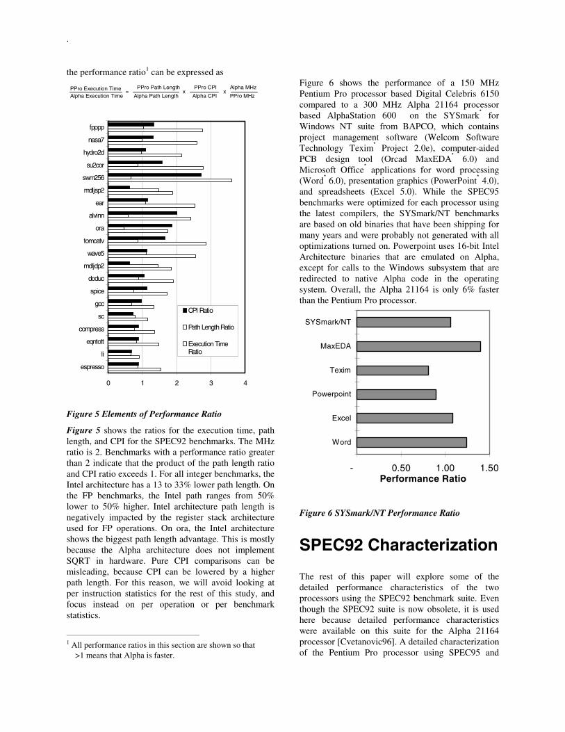
the performance ratio1 can be expressed as
PPro Execution TimeAlpha Execution Time
=PPro Path Length
Alpha Path Lengthx
PPro CPI
Alpha CPIx
PPro MHz
Alpha MHz
0 1 2 3 4
espresso
li
eqntott
compress
sc
gcc
spice
doduc
mdljdp2
wave5
tomcatv
ora
alvinn
ear
mdljsp2
swm256
su2cor
hydro2d
nasa7
fpppp
CPI Ratio
Path Length Ratio
Execution TimeRatio
Figure 5 Elements of Performance Ratio
Figure 5 shows the ratios for the execution time, pathlength, and CPI for the SPEC92 benchmarks. The MHzratio is 2. Benchmarks with a performance ratio greaterthan 2 indicate that the product of the path length ratioand CPI ratio exceeds 1. For all integer benchmarks, theIntel architecture has a 13 to 33% lower path length. Onthe FP benchmarks, the Intel path ranges from 50%lower to 50% higher. Intel architecture path length isnegatively impacted by the register stack architectureused for FP operations. On ora, the Intel architectureshows the biggest path length advantage. This is mostlybecause the Alpha architecture does not implementSQRT in hardware. Pure CPI comparisons can bemisleading, because CPI can be lowered by a higherpath length. For this reason, we will avoid looking atper instruction statistics for the rest of this study, andfocus instead on per operation or per benchmarkstatistics.
1 All performance ratios in this section are shown so that
>1 means that Alpha is faster.
Figure 6 shows the performance of a 150 MHzPentium Pro processor based Digital Celebris 6150compared to a 300 MHz Alpha 21164 processorbased AlphaStation 600 on the SYSmark* forWindows NT suite from BAPCO, which containsproject management software (Welcom SoftwareTechnology Texim* Project 2.0e), computer-aidedPCB design tool (Orcad MaxEDA* 6.0) andMicrosoft Office* applications for word processing(Word* 6.0), presentation graphics (PowerPoint* 4.0),and spreadsheets (Excel 5.0). While the SPEC95benchmarks were optimized for each processor usingthe latest compilers, the SYSmark/NT benchmarksare based on old binaries that have been shipping formany years and were probably not generated with alloptimizations turned on. Powerpoint uses 16-bit IntelArchitecture binaries that are emulated on Alpha,except for calls to the Windows subsystem that areredirected to native Alpha code in the operatingsystem. Overall, the Alpha 21164 is only 6% fasterthan the Pentium Pro processor.
- 0.50 1.00 1.50
Word
Excel
Powerpoint
Texim
MaxEDA
SYSmark/NT
Performance Ratio
Figure 6 SYSmark/NT Performance Ratio
SPEC92 Characterization
The rest of this paper will explore some of thedetailed performance characteristics of the twoprocessors using the SPEC92 benchmark suite. Eventhough the SPEC92 suite is now obsolete, it is usedhere because detailed performance characteristicswere available on this suite for the Alpha 21164processor [Cvetanovic96]. A detailed characterizationof the Pentium Pro processor using SPEC95 and
.
SYSmark/NT can be found in another recentpublication [Bhandarkar97].
0 1000 2000 3000 4000 5000 6000 7000
espresso
li
eqntott
compress
sc
gcc
spice
doduc
mdljdp2
wave5
tomcatv
ora
alvinn
ear
mdljsp2
swm256
su2cor
hydro2d
nasa7
fpppp
Million Data References
Pentium Pro ProcessorAlpha 21164
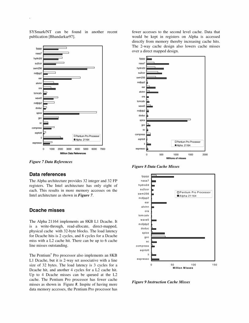
Figure 7 Data References
Data referencesThe Alpha architecture provides 32 integer and 32 FPregisters. The Intel architecture has only eight ofeach. This results in more memory accesses on theIntel architecture as shown in Figure 7.
Dcache misses
The Alpha 21164 implements an 8KB L1 Dcache. Itis a write-through, read-allocate, direct-mapped,physical cache with 32-byte blocks. The load latencyfor Dcache hits is 2 cycles, and 8 cycles for a Dcachemiss with a L2 cache hit. There can be up to 6 cacheline misses outstanding.
The Pentium Pro processor also implements an 8KBL1 Dcache, but it is 2-way set associative with a linesize of 32 bytes. The load latency is 3 cycles for aDcache hit, and another 4 cycles for a L2 cache hit.Up to 4 Dcache misses can be queued at the L2cache. The Pentium Pro processor has fewer cachemisses as shown in Figure 8. Inspite of having moredata memory accesses, the Pentium Pro processor has
fewer accesses to the second level cache. Data thatwould be kept in registers on Alpha is accesseddirectly from memory thereby increasing cache hits.The 2-way cache design also lowers cache missesover a direct mapped design.
0 500 1000 1500 2000
espresso
li
eqntott
compress
sc
gcc
spice
doduc
mdljdp2
wave5
tomcatv
ora
alvinn
ear
mdljsp2
swm256
su2cor
hydro2d
nasa7
fpppp
Millions of misses
Pentium Pro ProcessorAlpha 21164
Figure 8 Data Cache Misses
0 50 100 150
espresso
li
eqntott
com press
sc
gcc
spice
doduc
m dljdp2
wave5
tom catv
ora
alvinn
ear
m dljsp2
swm 256
su2cor
hydro2d
nasa7
fpppp
M illion M isses
Pentium Pro ProcessorAlpha 21164
Figure 9 Instruction Cache Misses
.
Icache missesThe instruction cache (Icache) in the Alpha 21164 isan 8KB, virtual, direct-mapped cache with 32-byteblocks. On the Pentium Pro processor, the instructioncache is also 8KB, but it is 4-way set associative witha line size of 32 bytes. Icache misses are also loweron the Pentium Pro processor as shown in Figure 9.The 4-way design and shorter instruction lengthsbenefit the Pentium Pro processor.
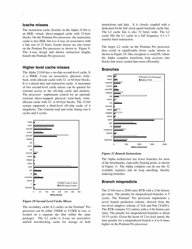
Higher level cache missesThe Alpha 21164 has a on-chip second-level cache. Itis a 96KB, 3-way set associative, physical, write-back, write-allocate cache with 32- or 64-byte blocks.It is a mixed data and instruction cache. A maximumof two second-level cache misses can be queued forexternal access to the off-chip cache and memory.The processor implements control for an optional,external, direct-mapped, physical, write-back, write-allocate cache with 32- or 64-byte blocks. The 21164system supported a third-level off-chip cache of 4megabytes. The external read and write timing was 6cycles and 5 cycles.
0 50 100 150 200 250 300 350
espresso
li
eqntott
compress
sc
gcc
spice
doduc
mdljdp2
wave5
tomcatv
ora
alvinn
ear
mdljsp2
swm256
su2cor
hydro2d
nasa7
fpppp
Million Misses
256KB 4-way L2 cache96 KB 3-way L2 cache
Figure 10 Second Level Cache Misses
The secondary cache (L2 cache) on the Pentium Proprocessor can be either 256KB or 512KB in size, islocated on a separate die (but within the samepackage). The L2 cache is 4-way set associativeunified non-blocking cache for storage of both
instructions and data. It is closely coupled with adedicated 64-bit full clock-speed backside cache bus.The L2 cache line is also 32 bytes wide. The L2cache fills the L1 cache in a full frequency 4-1-1-1transfer burst transaction.
The larger L2 cache on the Pentium Pro processordoes result in significantly fewer cache misses asshown in Figure 10. One exception is swm256, wherethe Alpha compiler transforms loop accesses intoblocks that reuse cached data more efficiently.
Branches
0 500 1000 1500 2000
espresso
li
eqntott
compress
sc
gcc
spice
doduc
mdljdp2
wave5
tomcatv
ora
alvinn
ear
mdljsp2
swm256
su2cor
hydro2d
nasa7
fpppp
Million Branches
Pentium Pro ProcessorAlpha 21164
Figure 11 Branch Instructions
The Alpha architecture has fewer branches for mostof the benchmarks, especially floating point, as shownin Figure 11. The Alpha compiler can do use the 32available registers and do loop unrolling, therebyreducing branches.
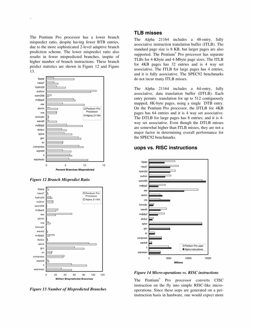
Branch mispredicts
The 21164 uses a 2048 entry BTB with a 2-bit historyper entry. The penalty for mispredicted branches is 5cycles. The Pentium Pro processor implements anovel branch prediction scheme, derived from thetwo-level adaptive scheme of Yeh and Patt [Yeh91].The BTB contains 512 entries with a 4-bit history perentry. The penalty for mispredicted branches is about10-15 cycles. Given the factor of 2 in clock speed, thetime penalty for a mispredicted branch is 4 to 6 timeshigher on the Pentium Pro processor.
.
The Pentium Pro processor has a lower branchmispredict ratio, despite having fewer BTB entries,due to the more sophisticated 2-level adaptive branchprediction scheme. The lower mispredict ratio alsoresults in fewer mispredicted branches, inspite ofhigher number of branch instructions. These branchpredict statistics are shown in Figure 12 and Figure13.
0 5 10 15
espresso
li
eqntott
compress
sc
gcc
spice
doduc
mdljdp2
wave5
tomcatv
ora
alvinn
ear
mdljsp2
swm256
su2cor
hydro2d
nasa7
fpppp
Percent Branches Mispredicted
Pentium ProProcessor
Alpha 21164
Figure 12 Branch Mispredict Ratio
0 20 40 60 80 100 120
espresso
li
eqntott
compress
sc
gcc
spice
doduc
mdljdp2
wave5
tomcatv
ora
alvinn
ear
mdljsp2
swm256
su2cor
hydro2d
nasa7
fpppp
Million Mispredicted Branches
Pentium ProProcessor
Alpha 21164
Figure 13 Number of Mispredicted Branches
TLB missesThe Alpha 21164 includes a 48-entry, fullyassociative instruction translation buffer (ITLB). Thestandard page size is 8 KB, but larger pages are alsosupported. The Pentium Pro processor has separateTLBs for 4-Kbyte and 4-Mbyte page sizes. The ITLBfor 4KB pages has 32 entries and is 4 way setassociative. The ITLB for large pages has 4 entries,and it is fully associative. The SPEC92 benchmarksdo not incur many ITLB misses.
The Alpha 21164 includes a 64-entry, fullyassociative, data translation buffer (DTLB). Eachentry permits translation for up to 512 contiguouslymapped, 8K-byte pages, using a single DTB entry.On the Pentium Pro processor, the DTLB for 4KBpages has 64 entries and it is 4 way set associative.The DTLB for large pages has 8 entries; and it is 4-way set associative. Even though the DTLB missesare somewhat higher than ITLB misses, they are not amajor factor in determining overall performance forthe SPEC92 benchmarks.
uops vs. RISC instructions
0 5000 10000 15000
espresso
li
eqntott
compress
sc
gcc
spice
doduc
mdljdp2
wave5
tomcatv
ora
alvinn
ear
mdljsp2
swm256
su2cor
hydro2d
nasa7
fpppp
Millions
Pentium Pro uopsAlpha instructions
Figure 14 Micro-operations vs. RISC instructions
The Pentium Pro processor converts CISCinstruction on the fly into simple RISC-like micro-operations. Since these uops are generated on a per-instruction basis in hardware, one would expect more

.
uops than a compiler could generate. Figure 14 showsthe uop count versus the RISC instructions. Forinteger benchmarks and spice (lowest FP content), theuops are fairly close to RISC instructions. On FPbenchmarks, in most cases there are fewer RISCinstructions. One notable exception is ora, whereAlpha has to generate multiple instructions tocalculate SQRT.
Accounting for all cyclesIt is interesting to analyze where all the time is spent.The Alpha 21164 is an in-order execution machinewith non-blocking caches. Some cache misses can beoverlapped with the execution of subsequentinstructions until a data dependency is encountered.Figure 15 shows where all the cycles are spent -issuing 1, 2, 3, or 4 instructions, or being stalled.Stalls are separated into either dry (Istream stalls andbranch mispredicts) or frozen (Dstream stalls, registerconflicts, execution units busy). About 30 to 50% ofthe time is spent in stalls on the SPEC integerbenchmarks, 45 to 63% on most SPEC FPbenchmarks, and 80% on the debit-credit transactionprocessing workload.
0% 20% 40% 60% 80% 100%
tpcb1
espresso
li
eqntott
compress
sc
gcc
spice
doduc
mdljdp2
wave5
tomcatv
ora
alvinn
ear
mdljsp2
swm256
su2cor
hydro2d
nasa7
fpppp
frozen
dry
quad issue
triple issue
dual issue
single issue
Figure 15 Issue and Stall cycles for Alpha 21164
Accounting for cycles in an out-of-order machine likethe Pentium Pro processor is more difficult due to allthe overlapped execution. It is still useful to examinethe various components of execution and stalls andcompare them to the actual cycles per instruction asshown in Figure 16. The CPI is generally much lowerthan the individual components due to overlappedexecution. The figure also shows resource stall cycles
in which some resource such as execution unit orbuffer entry is not available. Execution can proceedduring a resource stall cycle in some other part of themachine.
0
1
2
3
4
5
6
esp
ress
o li
eqn
tott
com
pres
s sc gcc
spic
e2g6
dodu
c
mdl
jdp2
wav
e5
tom
catv
ora
alv
inn
ear
mdl
jsp2
swm
256
su2c
or
hydr
o2d
nasa
7
fppp
p
Cyc
les
-
1
2
3
4
5
6
UOPS
Resource Stalls
Branch mispredicts
ITLB Misses
DTLB Misses
L2 Misses
L1 Inst Misses
L1 Data Misses
CPI
Figure 16 CPI vs. Stalls for Pentium Pro processor
OLTP PerformanceWe have presented CPU performance comparisonsfor the SPEC92 benchmarks. Most of thesebenchmarks show good locality of instruction anddata references. Many commercial workloads exhibitvery different memory access patterns that result inmore cache misses and significant stall times formemory as shown in Figure 15. On Line TransactionProcessing (OLTP) benchmarks like TPC-C modelI/O intensive environments which stress the memorysystems of machines much more thoroughly. TPC-Csimulates a complete computing environment where apopulation of terminal operators executes transactionsagainst a database. The benchmark is centered aroundthe principal activities (transactions) of an order-entryenvironment. These transactions include entering anddelivering orders, recording payments, checking thestatus of orders, and monitoring the level of stock atthe warehouses.
No measured data is available for the chips we havestudied in this paper, but there is data on derivativesof both chips, which are essentially shrinks to the nextgeneration 0.35µ technology running at a 33% fasterclock rate. Table 4 shows the highest reported TPC-Cperformance (measured in transactions per minute) ofquad processor systems, based on the 400 MHz

.
Alpha 21164 (12.1 SPECint95) and 200 MHzPentium Pro (8.71 SPECint95) processors, circaOctober 1996. The results show that while the Alphasystem is 45% faster on SPECint_rate95, it is 8%slower on the TPC-C benchmark with a 59% higher$/tpmC using the same database software!
Table 4 TPC-C Performance
CompaqProLiant 5000Model 6/200
DigitalAlphaServer4100 5/400
CPUs Four 200 MHzPentium Proprocessors
Four 400 MHzAlpha 21164processors
L2 cache 512KB 4 MBSPECint_rate95 292 (est)2 422TPC-C perf 8311 tpmC @
$95.32/tpmC7598 tpmC @$152.04/tpmC
Operating Sys SCO UnixWare Digital UNIXDatabase Sybase SQL
Server 11.0Sybase SQLServer 11.0
Concluding RemarksStudies like this one offer some insight into theperformance characteristics of different instruction setarchitectures and attempts to implement them well ina comparable technology. The overall performance isaffected by many factors and strict cause-effectrelationships are hard to pinpoint. Such explorationsare also hindered by the lack of measured data oncommon workloads for systems designed by differentcompanies. This study would have been moremeaningful if more stressful environments like on-line transaction processing and computer aided designcould have been analyzed in detail. Nevertheless, itdoes provide new quantitative data, that can be usedto get a better understanding of the performancedifferences between a premier RISC and CISCimplementation.
Using a comparable die size, the Pentium Proprocessor achieves 80 to 90% of the performance ofthe Alpha 21164 on integer benchmarks andtransaction processing workloads. It uses anaggressive out-of-order design to overcome theinstruction set level limitations of a CISCarchitecture. On floating-point intensive benchmarks,the Alpha 21164 does achieve over twice theperformance of the Pentium Pro processor.
2 measured result for Fujitsu ICL Superserver J654i using
the same processor.
AcknowledgmentsThe author is grateful to Jeff Reilly and Mason Guyof Intel for collecting the performance countermeasurement data for the Pentium Pro processor,and Zarka Cvetanovic of Digital EquipmentCorporation for providing the performance countermeasurement data for the Alpha 21164.
References[Bannon95] P. Bannon and J. Keller, “InternalArchitecture of Alpha 21164 Microprocessor”, Proc.Compcon Spring 95, Mar 1995.
[Bhandarkar91] D. Bhandarkar and D. Clark,“Performance from Architecture: Comparing a RISCand a CISC with Similar Hardware Organization,”Proceedings of ASPLOS-IV, April 1991.
[Bhandarkar95] D. Bhandarkar, “AlphaImplementations and Architecture: CompleteReference and Guide”, 1995, ISBN: 1-55558-130-7,Digital Press, Newton, MA.
[Bhandarkar97] D. Bhandarkar and J. Ding,“Performance Characterization of the Pentium ProProcessor,” Proceedings of HPCA-3, February 1997.
[Colwell95] R. Colwell and R. Steck, “A 0.6umBiCMOS Processor with Dynamic Execution”,ISSCC Proceedings, pp 176-177, February 1995.
[Cvetanovic96] Z. Cvetanovic and D. Bhandarkar,“Performance Characterization of the Alpha 21164Microprocessor using TP and SPEC Workloads,”Proceedings of HPCA-2, February 1996.
[Edmondson95] J. Edmondson et al, “SuperscalarInstruction Execution in the 21164 Microprocessor”,IEEE Micro, April 1995, pp.33-43.
[Papworth96] D. Papworth, “Tuning The Pentium
Pro Microarchitecture,” IEEE Micro, April 1996, pp.8-15.
[Yeh91] Tse-Yu Yeh and Yale Patt, “Two-LevelAdaptive Training Branch Prediction,” Proc. IEEEMicro-24, Nov 1991, pp. 51-61. * Intel® and Pentium® are registered trademarks ofIntel Corporation. Other brands and names are theproperty of their respective owners.