rm41l232 16- and 32-bit risc flash microcontroller ... sheets/texas...the device has a...
TRANSCRIPT

Product
Folder
Sample &Buy
Technical
Documents
Tools &
Software
Support &Community
RM41L232SPNS240A –OCTOBER 2014–REVISED JUNE 2015
RM41L232 16- and 32-Bit RISC Flash Microcontroller1 Device Overview
1.1 Features1
• High-Performance Microcontroller for Safety- • Multiple Communication InterfacesCritical Applications – Two CAN Controllers (DCANs)– Dual CPUs Running in Lockstep • DCAN1 - 32 Mailboxes With Parity– ECC on Flash and RAM Interfaces Protection– Built-In Self-Test for CPU and On-Chip RAMs • DCAN2 - 16 Mailboxes With Parity
Protection– Error Signaling Module With Error Pin• Compliant to CAN Protocol Version 2.0B– Voltage and Clock Monitoring
– Multibuffered Serial Peripheral Interface• ARM® Cortex®-R4 32-Bit RISC CPU(MibSPI) Module– Efficient 1.66 DMIPS/MHz With 8-Stage Pipeline• 128 Words With Parity Protection– 8-Region Memory Protection Unit (MPU)
– Two Standard Serial Peripheral Interface (SPI)– Open Architecture With Third-Party SupportModules• Operating Conditions
– UART (SCI) Interface With Local Interconnect– 80-MHz System Clock Network (LIN 2.1) Interface Support– Core Supply Voltage (VCC): 1.2-V Nominal • Next Generation High-End Timer (N2HET) Module– I/O Supply Voltage (VCCIO): 3.3-V Nominal – Up to 19 Programmable Pins– ADC Supply Voltage (VCCAD): 3.3-V Nominal – 128-Word Instruction RAM With Parity• Integrated Memory Protection– 128KB of Program Flash With ECC – Includes Hardware Angle Generator– 32KB of RAM With ECC – Dedicated High-End Timer Transfer Unit (HTU)– 16KB of Flash for Emulated EEPROM With With MPU
ECC • Enhanced Quadrature Encoder Pulse (eQEP)• Hercules™ Common Platform Architecture Module
– Consistent Memory Map Across Family – Motor Position Encoder Interface– Real-Time Interrupt (RTI) Timer (OS Timer) • 12-Bit Multibuffered Analog-to-Digital Converter– 96-Channel Vectored Interrupt Module (VIM) (ADC) Module– 2-Channel Cyclic Redundancy Checker (CRC) – 16 Channels
• Frequency-Modulated Phase-Locked Loop – 64 Result Buffers With Parity Protection(FMPLL) With Built-In Slip Detector • Up to 45 General-Purpose Input/Output (GPIO)
• IEEE 1149.1 JTAG Boundary Scan and ARM PinsCoreSight™ Components – 8 Dedicated Interrupt-Capable GPIO Pins
• Advanced JTAG Security Module (AJSM) • Package– 100-Pin Quad Flatpack (PZ) [Green]
1
An IMPORTANT NOTICE at the end of this data sheet addresses availability, warranty, changes, use in safety-critical applications,intellectual property matters and other important disclaimers. PRODUCTION DATA.
RM41L232SPNS240A –OCTOBER 2014–REVISED JUNE 2015 www.ti.com
1.2 Applications• Industrial Safety Applications • Medical Applications
– Industrial Automation – Ventilators– Safe Programmable Logic Controllers (PLCs) – Defibrillators– Power Generation and Distribution – Infusion and Insulin Pumps– Turbines and Windmills – Radiation Therapy– Elevators and Escalators – Robotic Surgery
2 Device Overview Copyright © 2014–2015, Texas Instruments IncorporatedSubmit Documentation FeedbackProduct Folder Links: RM41L232
RM41L232www.ti.com SPNS240A –OCTOBER 2014–REVISED JUNE 2015
1.3 DescriptionThe RM41L232 device is a high-performance microcontroller for safety systems. The safety architectureincludes dual CPUs in lockstep, CPU and Memory BIST logic, ECC on both the flash and the data SRAM,parity on peripheral memories, and loopback capability on peripheral I/Os.
The RM41L232 device integrates the ARM Cortex-R4 CPU. The CPU offers an efficient 1.66 DMIPS/MHz,and has configurations that can run up to 80 MHz, providing up to 132 DMIPS. The device operates inlittle-endian (LE) mode.
The RM41L232 device has 128KB of integrated flash and 32KB of data RAM. Both the flash and RAMhave single-bit error correction and double-bit error detection. The flash memory on this device is anonvolatile, electrically erasable, and programmable memory implemented with a 64-bit-wide data businterface. The flash operates on a 3.3-V supply input (the same level as I/O supply) for all read, program,and erase operations. When in pipeline mode, the flash operates with a system clock frequency of 80MHz. The SRAM supports single-cycle read and write accesses in byte, halfword, word, and double-wordmodes throughout the supported frequency range.
The RM41L232 device features peripherals for real-time control-based applications, including a NextGeneration High-End Timer (N2HET) timing coprocessor with up to 19 I/O terminals and a 12-bit Analog-to-Digital Converter (ADC) supporting 16 inputs in the 100-pin package.
The N2HET is an advanced intelligent timer that provides sophisticated timing functions for real-timeapplications. The timer is software-controlled, using a small instruction set, with a specialized timermicromachine and an attached I/O port. The N2HET can be used for pulse-width-modulated outputs,capture or compare inputs, or GPIO. The N2HET is especially well suited for applications requiringmultiple sensor information and drive actuators with complex and accurate time pulses. A High-End TimerTransfer Unit (HTU) can perform DMA-type transactions to transfer N2HET data to or from main memory.A Memory Protection Unit (MPU) is built into the HTU.
The Enhanced Quadrature Encoder Pulse (eQEP) module is used for direct interface with a linear orrotary incremental encoder to get position, direction, and speed information from a rotating machine asused in high-performance motion and position-control systems.
The device has a 12-bit-resolution MibADC with 16 channels and 64 words of parity-protected buffer RAM.The MibADC channels can be converted individually or can be grouped by software for sequentialconversion sequences. There are three separate groupings. Each sequence can be converted once whentriggered or configured for continuous conversion mode. The MibADC has a 10-bit mode for use whencompatibility with older devices or faster conversion time is desired.
The device has multiple communication interfaces: one MibSPI, two SPIs, one UART/LIN, and twoDCANs. The SPI provides a convenient method of serial high-speed communications between similarshift-register type devices. The UART/LIN supports the Local Interconnect standard 2.1 and can be usedas a UART in full-duplex mode using the standard Non-Return-to-Zero (NRZ) format. The DCAN supportsthe CAN 2.0 (A and B) protocol standard and uses a serial, multimaster communication protocol thatefficiently supports distributed real-time control with robust communication rates of up to 1 Mbps. TheDCAN is ideal for applications operating in noisy and harsh environments (for example, automotive andindustrial applications) that require reliable serial communication or multiplexed wiring.
The Frequency-Modulated Phase-Locked Loop (FMPLL) clock module is used to multiply the externalfrequency reference to a higher frequency for internal use. The FMPLL provides one of the five possibleclock source inputs to the Global Clock Module (GCM). The GCM manages the mapping between theavailable clock sources and the device clock domains.
The device also has an External Clock Prescaler (ECP) module that when enabled, outputs a continuousexternal clock on the ECLK pin. The ECLK frequency is a user-programmable ratio of the peripheralinterface clock (VCLK) frequency. This low-frequency output can be monitored externally as an indicator ofthe device operating frequency.
Copyright © 2014–2015, Texas Instruments Incorporated Device Overview 3Submit Documentation FeedbackProduct Folder Links: RM41L232
RM41L232SPNS240A –OCTOBER 2014–REVISED JUNE 2015 www.ti.com
The Error Signaling Module (ESM) monitors all device errors and determines whether an interrupt isgenerated or the external nERROR pin is toggled when a fault is detected. The nERROR pin can bemonitored externally as an indicator of a fault condition in the microcontroller.
The I/O Multiplexing and Control Module (IOMM) allows the configuration of the input/output pins tosupport alternate functions. See Table 4-17 for a list of the pins that support multiple functions on thisdevice.
With integrated safety features and a wide choice of communication and control peripherals, theRM41L232 device is an ideal solution for real-time control applications with safety-critical requirements.
Device Information (1)
PART NUMBER PACKAGE BODY SIZERM41L232PZ LQFP (100) 14.00 mm × 14.00 mm
(1) For more information, see Section 9, Mechanical Packaging and Orderable Information.
4 Device Overview Copyright © 2014–2015, Texas Instruments IncorporatedSubmit Documentation FeedbackProduct Folder Links: RM41L232

ESM
Flash128KBwith ECC
CRC2 Channel
PeripheralBridge
PCR
N2HET128 Wordswith Parity
SYS
GIO
LIN
MiBSPI18 Transfer
Groups
128 Bufferswith Parity
DCAN132 Messages
with Parity
nTRST
TMS
TCK
TDI
TDO
nRSTnPORRSTTEST
N2HET[31:28, 26, 24:22, 20:16,14, 12, 10, 8, 6, 4, 2, 0]
GIOA[7:0]/INT[7:0]
LINRXLINTX
MIBSPI1SIMOMIBSPI1SOMIMIBSPI1CLKMIBSPI1nCS[3:0]
CAN1RXCAN1TX
FLTP1
ECLK
DCAN216 Messages
with Parity
CAN2RXCAN2TX
VIM96 Channelwith Parity
CCM-R4RTCK
nERROR
MIBSPI1nENA
FLTP2
RAM32KB
with ECC
R4Slave I/F
RTI
MiBADC64 Wordswith Parity
ADIN[21, 20, 17, 16, 11:0]
VCCAD /ADREFHIVSSAD /ADREFLO
ADEVT
SPI2SPI2SIMOSPI2SOMISPI2CLKSPI2nCS[0]
STCLBIST
DebugGasket
SCR
DAPwith
ICEPick
HTU2 Regions
8 DCPwith MPU
BRIDGE
Cortex-R4with MPU8 regions
16KBFlash forEEPROM
w/ECC
VCCP
Cortex-R4with MPU8 regions
OSCIN
OSCOUT
VCCPLL
VSSPLL
Kelvin_GND
OSCPLL
ClockMonitor
AJSM
eQEPDCCIOMM
eQ
EP
Ae
QE
PB
eQ
EP
Se
QE
PI
SPI3
SPI3SIMOSPI3SOMISPI3CLKSPI3nCS[3:0]SPI3nENA
RM41L232www.ti.com SPNS240A –OCTOBER 2014–REVISED JUNE 2015
1.4 Functional Block DiagramFigure 1-1 shows a functional block diagram of the device.
Figure 1-1. Functional Block Diagram
Copyright © 2014–2015, Texas Instruments Incorporated Device Overview 5Submit Documentation FeedbackProduct Folder Links: RM41L232
RM41L232SPNS240A –OCTOBER 2014–REVISED JUNE 2015 www.ti.com
Table of Contents1 Device Overview ......................................... 1 6.9 Flash Memory ....................................... 49
6.10 Flash Program and Erase Timings for Program1.1 Features .............................................. 1Flash ................................................ 511.2 Applications........................................... 2
6.11 Flash Program and Erase Timings for Data Flash.. 511.3 Description............................................ 36.12 Tightly Coupled RAM Interface Module ............. 521.4 Functional Block Diagram ............................ 56.13 Parity Protection for Accesses to peripheral RAMs. 522 Revision History ......................................... 76.14 On-Chip SRAM Initialization and Testing ........... 533 Device Comparison ..................................... 86.15 Vectored Interrupt Manager ......................... 554 Terminal Configuration and Functions ............. 96.16 Real-Time Interrupt Module ......................... 574.1 PZ QFP Package Pinout (100-Pin) ................... 96.17 Error Signaling Module .............................. 584.2 Terminal Functions ................................. 106.18 Reset / Abort / Error Sources ....................... 624.3 Output Multiplexing and Control..................... 166.19 Digital Windowed Watchdog ........................ 634.4 Special Multiplexed Options......................... 176.20 Debug Subsystem................................... 645 Specifications .......................................... 18
7 Peripheral Information and Electrical5.1 Absolute Maximum Ratings ......................... 18Specifications ........................................... 69
5.2 ESD Ratings ........................................ 187.1 Peripheral Legend................................... 69
5.3 Power-On Hours (POH)............................. 187.2 Multibuffered 12-Bit Analog-to-Digital Converter .... 69
5.4 Recommended Operating Conditions............... 197.3 General-Purpose Input/Output ...................... 775.5 Switching Characteristics Over Recommended7.4 Enhanced High-End Timer (N2HET) ................ 78Operating Conditions for Clock Domains ........... 197.5 Controller Area Network (DCAN).................... 815.6 Wait States Required ............................... 207.6 Local Interconnect Network Interface (LIN) ......... 825.7 Power Consumption ................................ 217.7 Multibuffered / Standard Serial Peripheral Interface 835.8 Thermal Resistance Characteristics for PZ ......... 227.8 Enhanced Quadrature Encoder (eQEP) ............ 935.9 Input/Output Electrical Characteristics .............. 22
8 Device and Documentation Support ............... 955.10 Output Buffer Drive Strengths ...................... 238.1 Device Support ...................................... 955.11 Input Timings........................................ 248.2 Documentation Support ............................. 975.12 Output Timings ...................................... 258.3 Community Resources .............................. 976 System Information and Electrical
Specifications ........................................... 27 8.4 Trademarks.......................................... 976.1 Voltage Monitor Characteristics ..................... 27 8.5 Electrostatic Discharge Caution..................... 976.2 Power Sequencing and Power-On Reset ........... 28 8.6 Glossary ............................................. 976.3 Warm Reset (nRST)................................. 30 8.7 Device Identification Code Register................. 976.4 ARM Cortex-R4 CPU Information ................... 31 8.8 Die Identification Registers ......................... 986.5 Clocks ............................................... 35 8.9 Module Certifications ................................ 996.6 Clock Monitoring .................................... 41 9 Mechanical Packaging and Orderable
Addendum.............................................. 1046.7 Glitch Filters ......................................... 439.1 Packaging Information ............................. 1046.8 Device Memory Map ................................ 44
6 Table of Contents Copyright © 2014–2015, Texas Instruments IncorporatedSubmit Documentation FeedbackProduct Folder Links: RM41L232

RM41L232www.ti.com SPNS240A –OCTOBER 2014–REVISED JUNE 2015
2 Revision HistoryScope: Applicable updates to the Hercules™ MCU device family, specifically relating to the RM41L232devices, which are now in the production data (PD) stage of development have been incorporated.
Changes from April 30, 2014 to June 30, 2015 (from Initial Revision (April 2014) to A Revision) Page
• Updated/Changed section title to "Device Overview" ........................................................................... 1• Added Section 1.3 (Description): Added paragraph describing IOMM ....................................................... 4• Section 1.3 (Description): Added the Device Information table................................................................. 4• Added Section 3, Device Comparison ............................................................................................. 8• Section 5.1 Absolute Maximum Ratings): Moved Storage temperature range, Tstg from Section 5.2 ESD Ratings ... 18• Section 5.2 (ESD Ratings): Updated/Changed section title ................................................................... 18• Section 5.3 (Power-On Hours (POH)): Added table (new) .................................................................... 18• Table 5-4 (Selectable 8mA/2mA Control): Clarified impact of SPI2PC9 register on drive strength of SPI2SOMI
pin in footnote........................................................................................................................ 23• Section 6.4.1 (Summary of ARM Cortex-R4 CPU Features): Added Quantity of Breakpoints and Watchpoints ...... 31• Section 6.20.3 (JTAG Identification Code): Added a table showing JTAG ID code for each silicon revision. .......... 64• Table 7-7 (MibADC Operating Characteristics ): Added missing footnote for ZSET 10-/12-bit modes. ................... 73• Section 7.7.1 (Features [MibSPI]): Updated/Changed size of SPI baud clock generator from "8-bit" to "11-bit"....... 83• Figure 8-1 (Device Numbering Conventions): Updated/Change figure to include "Die Revision" ........................ 96• Section 8.2.1 (Related Documentation from Texas Instruments): Added reference documents ......................... 97• Section 8.7 (Device Identification Code Register): Added silicon revision B device identification code ................. 97• Section 8.8 (Die Identification Registers): Updated/Changed the DIEIDL and DIEIDH to point to the original
registers at location 0xFFFFFF7C and 0xFFFFFF80 .......................................................................... 98
Copyright © 2014–2015, Texas Instruments Incorporated Revision History 7Submit Documentation FeedbackProduct Folder Links: RM41L232
RM41L232SPNS240A –OCTOBER 2014–REVISED JUNE 2015 www.ti.com
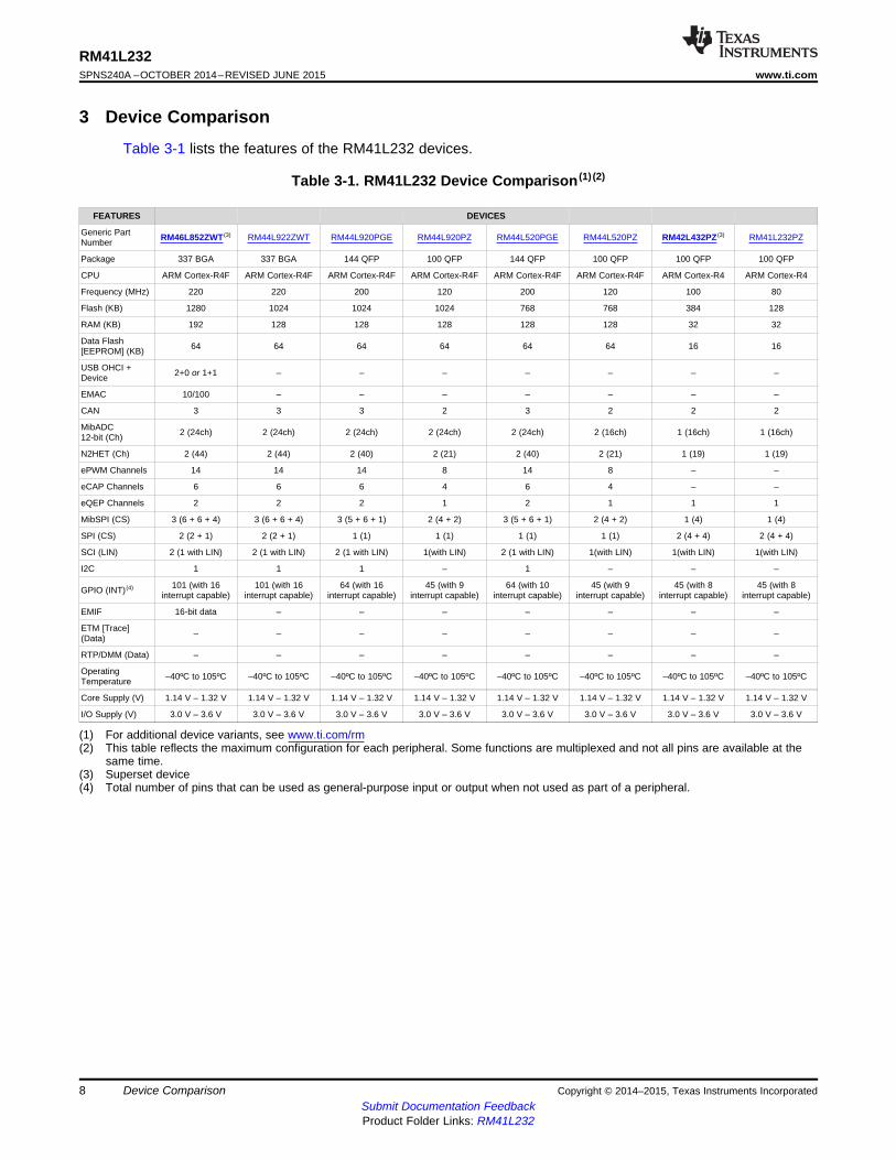
3 Device Comparison
Table 3-1 lists the features of the RM41L232 devices.
Table 3-1. RM41L232 Device Comparison (1) (2)
FEATURES DEVICES
Generic Part RM46L852ZWT (3) RM44L922ZWT RM44L920PGE RM44L920PZ RM44L520PGE RM44L520PZ RM42L432PZ (3) RM41L232PZNumber
Package 337 BGA 337 BGA 144 QFP 100 QFP 144 QFP 100 QFP 100 QFP 100 QFP
CPU ARM Cortex-R4F ARM Cortex-R4F ARM Cortex-R4F ARM Cortex-R4F ARM Cortex-R4F ARM Cortex-R4F ARM Cortex-R4 ARM Cortex-R4
Frequency (MHz) 220 220 200 120 200 120 100 80
Flash (KB) 1280 1024 1024 1024 768 768 384 128
RAM (KB) 192 128 128 128 128 128 32 32
Data Flash 64 64 64 64 64 64 16 16[EEPROM] (KB)
USB OHCI + 2+0 or 1+1 – – – – – – –Device
EMAC 10/100 – – – – – – –
CAN 3 3 3 2 3 2 2 2
MibADC 2 (24ch) 2 (24ch) 2 (24ch) 2 (24ch) 2 (24ch) 2 (16ch) 1 (16ch) 1 (16ch)12-bit (Ch)
N2HET (Ch) 2 (44) 2 (44) 2 (40) 2 (21) 2 (40) 2 (21) 1 (19) 1 (19)
ePWM Channels 14 14 14 8 14 8 – –
eCAP Channels 6 6 6 4 6 4 – –
eQEP Channels 2 2 2 1 2 1 1 1
MibSPI (CS) 3 (6 + 6 + 4) 3 (6 + 6 + 4) 3 (5 + 6 + 1) 2 (4 + 2) 3 (5 + 6 + 1) 2 (4 + 2) 1 (4) 1 (4)
SPI (CS) 2 (2 + 1) 2 (2 + 1) 1 (1) 1 (1) 1 (1) 1 (1) 2 (4 + 4) 2 (4 + 4)
SCI (LIN) 2 (1 with LIN) 2 (1 with LIN) 2 (1 with LIN) 1(with LIN) 2 (1 with LIN) 1(with LIN) 1(with LIN) 1(with LIN)
I2C 1 1 1 – 1 – – –
101 (with 16 101 (with 16 64 (with 16 45 (with 9 64 (with 10 45 (with 9 45 (with 8 45 (with 8GPIO (INT) (4)interrupt capable) interrupt capable) interrupt capable) interrupt capable) interrupt capable) interrupt capable) interrupt capable) interrupt capable)
EMIF 16-bit data – – – – – – –
ETM [Trace] – – – – – – – –(Data)
RTP/DMM (Data) – – – – – – – –
Operating –40ºC to 105ºC –40ºC to 105ºC –40ºC to 105ºC –40ºC to 105ºC –40ºC to 105ºC –40ºC to 105ºC –40ºC to 105ºC –40ºC to 105ºCTemperature
Core Supply (V) 1.14 V – 1.32 V 1.14 V – 1.32 V 1.14 V – 1.32 V 1.14 V – 1.32 V 1.14 V – 1.32 V 1.14 V – 1.32 V 1.14 V – 1.32 V 1.14 V – 1.32 V
I/O Supply (V) 3.0 V – 3.6 V 3.0 V – 3.6 V 3.0 V – 3.6 V 3.0 V – 3.6 V 3.0 V – 3.6 V 3.0 V – 3.6 V 3.0 V – 3.6 V 3.0 V – 3.6 V
(1) For additional device variants, see www.ti.com/rm(2) This table reflects the maximum configuration for each peripheral. Some functions are multiplexed and not all pins are available at the
same time.(3) Superset device(4) Total number of pins that can be used as general-purpose input or output when not used as part of a peripheral.
8 Device Comparison Copyright © 2014–2015, Texas Instruments IncorporatedSubmit Documentation FeedbackProduct Folder Links: RM41L232
MIBSPI1nCS[1]
VCCP
LINRX
VCCIOECLK
RTCK
26
27
28
29
30
31
32
33
34
35
36
37
38
39
40
41
42
43
44
45
46
47
48
49
50
N2HET[6]
MIBSPI1nCS[2]
VCCIO
VSS
VCC
nPORRST
VCC
VSS
SPI3nENA
ADIN[21]
TCK
SPI3nCS[0]
MIBSPI1nCS[3]
ADIN[0]
ADIN[7]
ADIN[20]
VSSAD/ADREFLO
ADIN[9]
VCCAD/ADREFHI
ADIN[1]
ADIN[10]
VSS
VCC
CAN2RX
CAN2TX
VCC
VSS
nERROR
nRST
TDO
TDI
nTRST
VSS
LINTX
SPI3CLK
AD
IN[2
]
AD
IN[3
]
AD
IN[4
]
AD
IN[5
]
AD
IN[6
]
AD
EV
T
VS
S
CA
N1T
X
CA
N1
RX
MIB
SP
I1S
OM
I
MIB
SP
I1C
LKM
IBS
PI1
nE
NA
SP
I2S
OM
I
SP
I2S
IMO
SP
I2C
LK
MIB
SP
I1n
CS
[0]
TM
S
VC
C
MIB
SP
I1S
IMO
VC
CIO
25
24
23
22
21
20
19
18
17
16
15
14
13
12
11
10
987654321
51
52
54
55
56
57
58
59
60
61
62
63
64
65
66
67
68
69
70
71
72
73
74
75
53
GIO
A[3
]
VS
SV
CC
IO
GIO
A[1
]
TE
ST
SP
I2n
CS
[0]
GIO
A[7
]
VS
S
KE
LVIN
_G
ND
OS
CIN
VC
CG
IOA
[6]
GIO
A[5
]
GIO
A[2
]
FLT
P2
FLT
P1
GIO
A[0
]
GIO
A[4
]
OS
CO
UT
100
99
98
97
96
95
94
93
92
91
90
89
88
87
86
85
84
83
82
81
80
79
78
77
76
VS
S
VC
C
VS
S
SPI3SOMISPI3SIMO
ADIN[16]
ADIN[17]
AD
IN[1
1]
AD
IN[8
]
N2H
ET
[4]
N2H
ET
[2]
N2H
ET
[0]
N2H
ET
[022]
N2H
ET
[024]
N2H
ET
[8]
N2HET[10]
N2H
ET
[8]
N2HET[14]
N2HET[12]
N2HET[16]
N2HET[18]
RM41L232www.ti.com SPNS240A –OCTOBER 2014–REVISED JUNE 2015
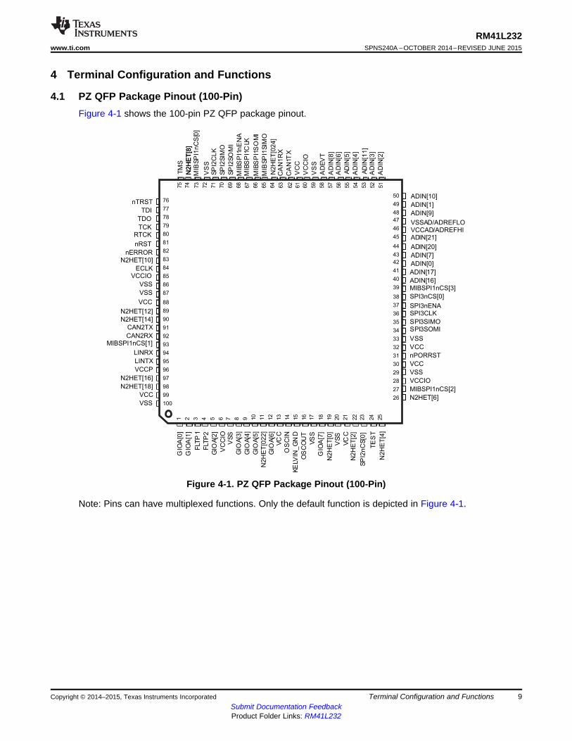
4 Terminal Configuration and Functions
4.1 PZ QFP Package Pinout (100-Pin)Figure 4-1 shows the 100-pin PZ QFP package pinout.
Figure 4-1. PZ QFP Package Pinout (100-Pin)
Note: Pins can have multiplexed functions. Only the default function is depicted in Figure 4-1.
Copyright © 2014–2015, Texas Instruments Incorporated Terminal Configuration and Functions 9Submit Documentation FeedbackProduct Folder Links: RM41L232

RM41L232SPNS240A –OCTOBER 2014–REVISED JUNE 2015 www.ti.com
4.2 Terminal FunctionsTable 4-1 through Table 4-16 identify the external signal names, the associated pin numbers along withthe mechanical package designator, the pin type (Input, Output, I/O, Power, or Ground), whether the pinhas any internal pullup/pulldown, whether the pin can be configured as a GPIO, and a functional pindescription.
NOTEIn the Terminal Functions table below, the "Reset Pull State" is the state of the pull applied tothe terminal while nPORRST is low and immediately after nPORRST goes High. The defaultpull direction may change when software configures the pin for an alternate function. The"Pull Type" is the type of pull asserted when the signal name in bold is enabled for the giventerminal by the IOMM control registers.
All I/O signals except nRST are configured as inputs while nPORRST is low andimmediately after nPORRST goes High. While nPORRST is low, the input buffersare disabled, and the output buffers are disabled with the default pulls enabled.
All output-only signals have the output buffer disabled and the default pull enabledwhile nPORRST is low, and are configured as outputs with the pulls disabledimmediately after nPORRST goes High.
4.2.1 High-End Timer (N2HET)
Table 4-1. High-End Timer (N2HET)
TERMINAL SIGNAL RESET PULL TYPE DESCRIPTIONTYPE PULLSIGNAL NAME 100 STATEPZ
N2HET[0] 19 I/O Pulldown Programmable, Timer input capture or output compare. The20 µA N2HET applicable terminals can be programmedN2HET[2] 22 as general-purpose input/output (GPIO).
N2HET[4] 25 Each terminal has a suppression filter with aprogrammable duration.N2HET[6] 26
N2HET[8] 74N2HET[10] 83N2HET[12] 89N2HET[14] 90N2HET[16] 97MIBSPI1nCS[1]/EQEPS/ 93N2HET[17]N2HET[18] 98MIBSPI1nCS[2]/N2HET[20]/ 27N2HET[19]MIBSPI1nCS[2]/N2HET[20]/ 27N2HET[19]N2HET[22] 11N2HET[24] 64MIBSPI1nCS[3]/N2HET[26] 39ADEVT/N2HET[28] 58GIOA[7]/N2HET[29] 18MIBSPI1nENA/N2HET[23]/ 68N2HET[30]GIOA[6]/SPI2nCS[1]/N2HET[31] 12
10 Terminal Configuration and Functions Copyright © 2014–2015, Texas Instruments IncorporatedSubmit Documentation FeedbackProduct Folder Links: RM41L232

RM41L232www.ti.com SPNS240A –OCTOBER 2014–REVISED JUNE 2015
4.2.2 Enhanced Quadrature Encoder Pulse Modules (eQEP)
Table 4-2. Enhanced Quadrature Encoder Pulse Modules (eQEP)
TERMINAL SIGNAL RESET PULL TYPE DESCRIPTIONTYPE PULLSIGNAL NAME 100 STATEPZ
SPI3CLK/EQEPA 36 Input Pullup Fixed 20 µA Enhanced QEP Input ASPI3nENA/EQEPB 37 Input Enhanced QEP Input BSPI3nCS[0]/EQEPI 38 I/O Enhanced QEP IndexMIBSPI1nCS[1]/EQEPS/N2HET 93 I/O Enhanced QEP Strobe[17]
4.2.3 General-Purpose Input/Output (GPIO)
Table 4-3. General-Purpose Input/Output (GPIO)
TERMINAL SIGNAL RESET PULL TYPE DESCRIPTIONTYPE PULLSIGNAL NAME 100 STATEPZ
GIOA[0]/SPI3nCS[3] 1 I/O Pulldown Programmable, General-purpose input/output20 µA All GPIO terminals can generate interrupts to theGIOA[1]/SPI3nCS[2] 2 CPU on rising/falling/both edges.
GIOA[2]/SPI3nCS[1] 5GIOA[3]/SPI2nCS[3] 8GIOA[4]/SPI2nCS[2] 9GIOA[5]/EXTCLKIN 10GIOA[6]/SPI2nCS[1]/N2HET[31] 12GIOA[7]/N2HET[29] 18
4.2.4 Controller Area Network Interface Modules (DCAN1, DCAN2)
Table 4-4. Controller Area Network Interface Modules (DCAN1, DCAN2)
TERMINAL SIGNAL RESET PULL TYPE DESCRIPTIONTYPE PULLSIGNAL NAME 100 STATEPZ
CAN1RX 63 I/O Pullup Programmable, CAN1 Receive, or general-purpose I/O (GPIO)20 µACAN1TX 62 CAN1 Transmit, or GPIO
CAN2RX 92 CAN2 Receive, or GPIOCAN2TX 91 CAN2 Transmit, or GPIO
Copyright © 2014–2015, Texas Instruments Incorporated Terminal Configuration and Functions 11Submit Documentation FeedbackProduct Folder Links: RM41L232

RM41L232SPNS240A –OCTOBER 2014–REVISED JUNE 2015 www.ti.com
4.2.5 Multibuffered Serial Peripheral Interface (MibSPI1)
Table 4-5. Multibuffered Serial Peripheral Interface (MibSPI1)
TERMINAL SIGNAL RESET PULL TYPE DESCRIPTIONTYPE PULLSIGNAL NAME 100 STATEPZ
MIBSPI1CLK 67 I/O Pullup Programmable, MibSPI1 Serial Clock, or GPIO20 µAMIBSPI1nCS[0] 73 MibSPI1 Chip Select, or GPIO
MIBSPI1nCS[1]/EQEPS/N2HET 93[17]MIBSPI1nCS[2]/N2HET[20]/N2 27HET[19]MIBSPI1nCS[3]/N2HET[26] 39MIBSPI1nENA/N2HET[23]/N2H 68 MibSPI1 Enable, or GPIOET[30]MIBSPI1SIMO 65 MibSPI1 Slave-In-Master-Out, or GPIOMIBSPI1SOMI 66 MibSPI1 Slave-Out-Master-In, or GPIO
4.2.6 Standard Serial Peripheral Interface (SPI2)
Table 4-6. Standard Serial Peripheral Interface (SPI2)
TERMINAL SIGNAL RESET PULL TYPE DESCRIPTIONTYPE PULLSIGNAL NAME 100 STATEPZ
SPI2CLK 71 I/O Pullup Programmable, SPI2 Serial Clock, or GPIO20 µASPI2nCS[0] 23 SPI2 Chip Select, or GPIO
GIOA[6]/SPI2nCS[1]/N2HET[31] 12GIOA[4]/SPI2nCS[2] 9GIOA[3]/SPI2nCS[3] 8SPI2SIMO 70 SPI2 Slave-In-Master-Out, or GPIOSPI2SOMI 69 SPI2 Slave-Out-Master-In, or GPIOThe drive strengths for the SPI2CLK, SPI2SIMO, and SPI2SOMI signals are selected individually by configuring the respective SRS bits ofthe SPIPC9 register fo SPI2.SRS = 0 for 8-mA drive (fast). This is the default mode as the SRS bits in the SPIPC9 register default to 0.SRS = 1 for 2-mA drive (slow)SPI3CLK/EQEPA 36 I/O Pullup Programmable, SPI3 Serial Clock, or GPIO
20 µASPI3nCS[0]/EQEPI 38 SPI3 Chip Select, or GPIOGIOA[2]/SPI3nCS[1] 5GIOA[1]/SPI3nCS[2] 2GIOA[0]/SPI3nCS[3] 1SPI3nENA/EQEPB 37 SPI3 Enable, or GPIOSPI3SIMO 35 SPI3 Slave-In-Master-Out, or GPIOSPI3SOMI 34 SPI3 Slave-Out-Master-In, or GPIO
4.2.7 Local Interconnect Network Controller (LIN)
Table 4-7. Local Interconnect Network Controller (LIN)
TERMINAL SIGNAL RESET PULL TYPE DESCRIPTIONTYPE PULLSIGNAL NAME 100 STATEPZ
LINRX 94 I/O Pullup Programmable, LIN Receive, or GPIO20 µALINTX 95 LIN Transmit, or GPIO
12 Terminal Configuration and Functions Copyright © 2014–2015, Texas Instruments IncorporatedSubmit Documentation FeedbackProduct Folder Links: RM41L232

RM41L232www.ti.com SPNS240A –OCTOBER 2014–REVISED JUNE 2015
4.2.8 Multibuffered Analog-to-Digital Converter (MibADC)
Table 4-8. Multibuffered Analog-to-Digital Converter (MibADC)
TERMINAL SIGNAL TYPE RESET PULL TYPE DESCRIPTIONPULLSIGNAL NAME 100 STATEPZ
ADEVT/N2HET[28] 58 I/O Pullup Programmable, ADC event trigger or GPIO20 µA
ADIN[0] 42 Input N/A None Analog inputsADIN[1] 49ADIN[2] 51ADIN[3] 52ADIN[4] 54ADIN[5] 55ADIN[6] 56ADIN[7] 43ADIN[8] 57ADIN[9] 48ADIN[10] 50ADIN[11] 53ADIN[16] 40ADIN[17] 41ADIN[20] 44ADIN[21] 45VCCAD/ADREFHI 46 Input/Power N/A None ADC high reference level/ADC operating supplyVSSAD/ADREFLO 47 Input/Ground N/A None ADC low reference level/ADC supply ground
4.2.9 System Module
Table 4-9. System Module
TERMINAL SIGNAL RESET PULL TYPE DESCRIPTIONTYPE PULLSIGNAL NAME 100 STATEPZ
ECLK 84 I/O Pulldown Programmable, External prescaled clock output, or GPIO.20 µA
GIOA[5]/EXTCLKIN 10 Input Pulldown 20 µA External Clock InnPORRST 31 Input Pulldown 100 µA Power-on reset, cold reset External power supply
monitor circuitry must drive nPORRST low whenany of the supplies to the microcontroller fall outof the specified range. This terminal has a glitchfilter.
nRST 81 I/O Pullup 100 µA The external circuitry can assert a system resetby driving nRST low. To ensure that an externalreset is not arbitrarily generated, TI recommendsthat an external pullup resistor is connected tothis terminal. This terminal has a glitch filter.
Copyright © 2014–2015, Texas Instruments Incorporated Terminal Configuration and Functions 13Submit Documentation FeedbackProduct Folder Links: RM41L232

RM41L232SPNS240A –OCTOBER 2014–REVISED JUNE 2015 www.ti.com
4.2.10 Error Signaling Module (ESM)
Table 4-10. Error Signaling Module (ESM)
TERMINAL SIGNAL RESET PULL TYPE DESCRIPTIONTYPE PULLSIGNAL NAME 100 STATEPZ
nERROR 82 I/O Pulldown 20 µA ESM error signal. Indicates error of high severity.
4.2.11 Main Oscillator
Table 4-11. Main Oscillator
TERMINAL SIGNAL RESET PULL TYPE DESCRIPTIONTYPE PULLSIGNAL NAME 100 STATEPZ
OSCIN 14 Input N/A None From external crystal/resonator, or external clockinput
OSCOUT 16 Output N/A None To external crystal/resonatorKELVIN_GND 15 Input N/A None Dedicated ground for oscillator
4.2.12 Test/Debug Interface
Table 4-12. Test/Debug Interface
TERMINAL SIGNAL RESET PULL TYPE DESCRIPTIONTYPE PULLSIGNAL NAME 100 STATEPZ
nTRST 76 Input Pulldown Fixed, 100 µA JTAG test hardware resetRTCK 80 Output N/A None JTAG return test clockTCK 79 Input Pulldown Fixed, 100 µA JTAG test clockTDI 77 I/O Pullup Fixed, 100 µA JTAG test data inTDO 78 Output Fixed, None JTAG test data out
100-µAPulldown
TMS 75 I/O Pullup Fixed, 100 µA JTAG test selectTEST 24 I/O Pulldown Fixed, 100 µA Test enable. This terminal must be connected to
ground directly or through a pulldown resistor.
4.2.13 Flash
Table 4-13. Flash
TERMINAL SIGNAL RESET PULL TYPE DESCRIPTIONTYPE PULLSIGNAL NAME 100 STATEPZ
FLTP1 3 Input N/A None Flash test pins. For proper operation this terminalmust connect only to a test pad or not beFLTP2 4 Input N/A None connected at all [no connect (NC)].The test pad must not be exposed in the finalproduct where it might be subjected to an ESDevent.
VCCP 96 3.3-V N/A None Flash external pump voltage (3.3 V). ThisPower terminal is required for both flash read and flash
program and erase operations.
14 Terminal Configuration and Functions Copyright © 2014–2015, Texas Instruments IncorporatedSubmit Documentation FeedbackProduct Folder Links: RM41L232
RM41L232www.ti.com SPNS240A –OCTOBER 2014–REVISED JUNE 2015
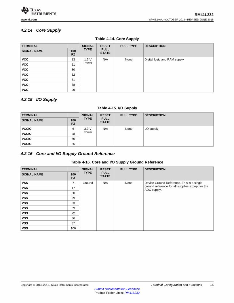
4.2.14 Core Supply
Table 4-14. Core Supply
TERMINAL SIGNAL RESET PULL TYPE DESCRIPTIONTYPE PULLSIGNAL NAME 100 STATEPZ
VCC 13 1.2-V N/A None Digital logic and RAM supplyPowerVCC 21
VCC 30VCC 32VCC 61VCC 88VCC 99
4.2.15 I/O Supply
Table 4-15. I/O Supply
TERMINAL SIGNAL RESET PULL TYPE DESCRIPTIONTYPE PULLSIGNAL NAME 100 STATEPZ
VCCIO 6 3.3-V N/A None I/O supplyPowerVCCIO 28
VCCIO 60VCCIO 85
4.2.16 Core and I/O Supply Ground Reference
Table 4-16. Core and I/O Supply Ground Reference
TERMINAL SIGNAL RESET PULL TYPE DESCRIPTIONTYPE PULLSIGNAL NAME 100 STATEPZ
VSS 7 Ground N/A None Device Ground Reference. This is a singleground reference for all supplies except for theVSS 17 ADC supply.
VSS 20VSS 29VSS 33VSS 59VSS 72VSS 86VSS 87VSS 100
Copyright © 2014–2015, Texas Instruments Incorporated Terminal Configuration and Functions 15Submit Documentation FeedbackProduct Folder Links: RM41L232
RM41L232SPNS240A –OCTOBER 2014–REVISED JUNE 2015 www.ti.com
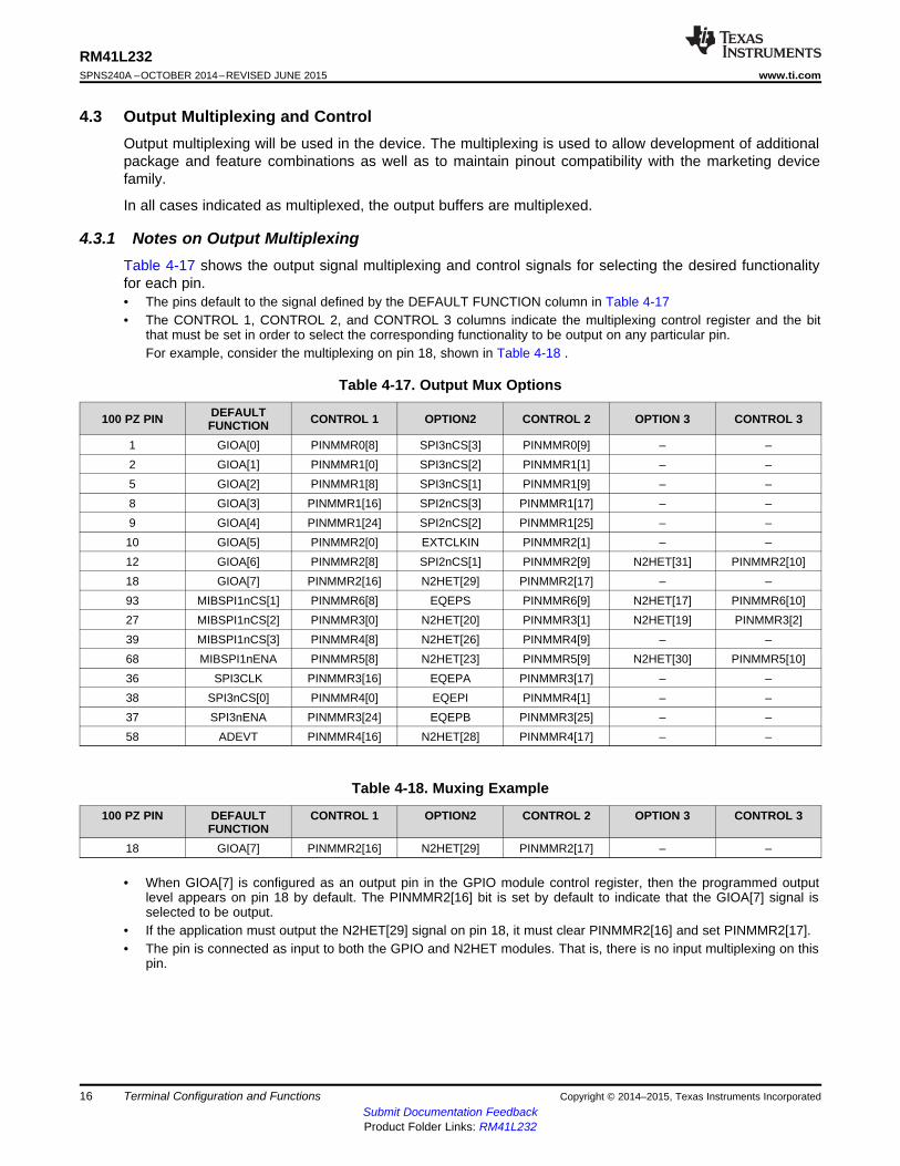
4.3 Output Multiplexing and ControlOutput multiplexing will be used in the device. The multiplexing is used to allow development of additionalpackage and feature combinations as well as to maintain pinout compatibility with the marketing devicefamily.
In all cases indicated as multiplexed, the output buffers are multiplexed.
4.3.1 Notes on Output MultiplexingTable 4-17 shows the output signal multiplexing and control signals for selecting the desired functionalityfor each pin.• The pins default to the signal defined by the DEFAULT FUNCTION column in Table 4-17• The CONTROL 1, CONTROL 2, and CONTROL 3 columns indicate the multiplexing control register and the bit
that must be set in order to select the corresponding functionality to be output on any particular pin.For example, consider the multiplexing on pin 18, shown in Table 4-18 .
Table 4-17. Output Mux Options
DEFAULT100 PZ PIN CONTROL 1 OPTION2 CONTROL 2 OPTION 3 CONTROL 3FUNCTION1 GIOA[0] PINMMR0[8] SPI3nCS[3] PINMMR0[9] – –2 GIOA[1] PINMMR1[0] SPI3nCS[2] PINMMR1[1] – –5 GIOA[2] PINMMR1[8] SPI3nCS[1] PINMMR1[9] – –8 GIOA[3] PINMMR1[16] SPI2nCS[3] PINMMR1[17] – –9 GIOA[4] PINMMR1[24] SPI2nCS[2] PINMMR1[25] – –10 GIOA[5] PINMMR2[0] EXTCLKIN PINMMR2[1] – –12 GIOA[6] PINMMR2[8] SPI2nCS[1] PINMMR2[9] N2HET[31] PINMMR2[10]18 GIOA[7] PINMMR2[16] N2HET[29] PINMMR2[17] – –93 MIBSPI1nCS[1] PINMMR6[8] EQEPS PINMMR6[9] N2HET[17] PINMMR6[10]27 MIBSPI1nCS[2] PINMMR3[0] N2HET[20] PINMMR3[1] N2HET[19] PINMMR3[2]39 MIBSPI1nCS[3] PINMMR4[8] N2HET[26] PINMMR4[9] – –68 MIBSPI1nENA PINMMR5[8] N2HET[23] PINMMR5[9] N2HET[30] PINMMR5[10]36 SPI3CLK PINMMR3[16] EQEPA PINMMR3[17] – –38 SPI3nCS[0] PINMMR4[0] EQEPI PINMMR4[1] – –37 SPI3nENA PINMMR3[24] EQEPB PINMMR3[25] – –58 ADEVT PINMMR4[16] N2HET[28] PINMMR4[17] – –
Table 4-18. Muxing Example
100 PZ PIN DEFAULT CONTROL 1 OPTION2 CONTROL 2 OPTION 3 CONTROL 3FUNCTION
18 GIOA[7] PINMMR2[16] N2HET[29] PINMMR2[17] – –
• When GIOA[7] is configured as an output pin in the GPIO module control register, then the programmed outputlevel appears on pin 18 by default. The PINMMR2[16] bit is set by default to indicate that the GIOA[7] signal isselected to be output.
• If the application must output the N2HET[29] signal on pin 18, it must clear PINMMR2[16] and set PINMMR2[17].• The pin is connected as input to both the GPIO and N2HET modules. That is, there is no input multiplexing on this
pin.
16 Terminal Configuration and Functions Copyright © 2014–2015, Texas Instruments IncorporatedSubmit Documentation FeedbackProduct Folder Links: RM41L232
RM41L232www.ti.com SPNS240A –OCTOBER 2014–REVISED JUNE 2015
4.3.2 General Rules for Multiplexing Control Registers• The PINMMR control registers can only be written in privileged mode. A write in a nonprivileged mode will
generate an error response.• If the application writes all 0s to any PINMMR control register, then the default functions are selected for the
affected pins.• Each byte in a PINMMR control register is used to select the functionality for a given pin. If the application sets
more than 1 bit within a byte for any pin, then the default function is selected for this pin.• Some bits within the PINMMR registers could be associated with internal pads that are not brought out in the 100-
pin package. As a result, bits marked reserved should not be written as 1.
4.4 Special Multiplexed OptionsSpecial controls are implemented to affect particular functions on this microcontroller. These controls aredescribed in this section.
4.4.1 Filtering for eQEP Inputs
4.4.1.1 eQEPA Input• When PINMMR8[0] = 1, the eQEPA input is double-synchronized using VCLK.• When PINMMR8[0] = 0 and PINMMR8[1] = 1, the eQEPA input is double-synchronized and then qualified through
a fixed 6-bit counter using VCLK.• PINMMR8[0] = 0 and PINMMR8[1] = 0 is an illegal combination and behavior defaults to PINMMR8[0] = 1.
4.4.1.2 eQEPB Input• When PINMMR8[8] = 1, the eQEPB input is double-synchronized using VCLK.• When PINMMR8[8] = 0 and PINMMR8[9] = 1, the eQEPB input is double-synchronized and then qualified through
a fixed 6-bit counter using VCLK.• PINMMR8[8] = 0 and PINMMR8[9] = 0 is an illegal combination and behavior defaults to PINMMR8[8] = 1.
4.4.1.3 eQEPI Input• When PINMMR8[16] = 1, the eQEPI input is double-synchronized using VCLK.• When PINMMR8[16] = 0 and PINMMR8[17] = 1, the eQEPI input is double-synchronized and then qualified
through a fixed 6-bit counter using VCLK.• PINMMR8[16] = 0 and PINMMR8[17] = 0 is an illegal combination and behavior defaults to PINMMR8[16] = 1.
4.4.1.4 eQEPS Input• When PINMMR8[24] = 1, the eQEPS input is double-synchronized using VCLK.• When PINMMR8[24] = 0 and PINMMR8[25] = 1, the eQEPS input is double-synchronized and then qualified
through a fixed 6-bit counter using VCLK.• PINMMR8[24] = 0 and PINMMR8[25] = 0 is an illegal combination and behavior defaults to PINMMR8[24] = 1.
4.4.2 N2HET PIN_nDISABLE Input Port• When PINMMR9[0] = 1, GIOA[5] is connected directly to N2HET PIN_nDISABLE input of the N2HET module.• When PINMMR9[0] = 0 and PINMMR9[1] = 1, EQEPERR is inverted and double-synchronized using VCLK before
connecting directly to the N2HET PIN_nDISABLE input of the N2HET module.• PINMMR9[0] = 0 and PINMMR9[1] = 0 is an illegal combination and behavior defaults to PINMMR9[0] = 1.
Copyright © 2014–2015, Texas Instruments Incorporated Terminal Configuration and Functions 17Submit Documentation FeedbackProduct Folder Links: RM41L232

RM41L232SPNS240A –OCTOBER 2014–REVISED JUNE 2015 www.ti.com
5 Specifications
5.1 Absolute Maximum Ratings (1)
Over Operating Free-Air Temperature RangeMIN MAX UNIT
VCC(2) –0.3 1.43
Supply voltage VCCIO, VCCP(2) –0.3 4.6 V
VCCAD –0.3 3.6All input pins –0.3 4.6
Input voltage VADC input pins –0.3 4.6IIK (VI < 0 or VI > VCCIO) –20 20All pins, except ADIN[21:20,17:16,11:0]
Input clamp current IIK (VI < 0 or VI > VCCAD) mA–10 10ADIN[21:20,17:16,11:0]Total –40 40
Operating free-air –40 105 °Ctemperature, TA
Operating junction –40 130 °Ctemperature, TJ
Latch-up performance I-test, All I/O pins –100 100 mAStorage temperature, Tstg –65 150 °C
(1) Stresses beyond those listed under Absolute Maximum Ratings may cause permanent damage to the device. These are stress ratingsonly, and functional operation of the device at these or any other conditions beyond those indicated under Recommended OperatingConditions is not implied. Exposure to absolute-maximum-rated conditions for extended periods may affect device reliability.
(2) Maximum-rated conditions for extended periods may affect device reliability. All voltage values are with respect to their associatedgrounds.
5.2 ESD RatingsVALUE UNIT
Human Body Model (HBM), per ANSI/ESDA/JEDEC JS001 (1) ±2 kVElectrostatic discharge (ESD)V(ESD) Charged Device Model (CDM), per JESD22-performance: All pins ±250 VC101 (2)
(1) JEDEC document JEP155 states that 500-V HBM allows safe manufacturing with a standard ESD control process.(2) JEDEC document JEP157 states that 250-V CDM allows safe manufacturing with a standard ESD control process.
5.3 Power-On Hours (POH) (1) (2)
JUNCTIONNOMINAL CORE VOLTAGE (VCC) LIFETIME POHTEMPERATURE (Tj)1.2 105ºC 100K
(1) This information is provided solely for your convenience and does not extend or modify the warranty provided under TI's standard termsand conditions for TI semiconductor products.
(2) To avoid significant degradation, the device power-on hours (POH) must be limited to those specified in this table. To convert toequivalent POH for a specific temperature profile, see the Calculating Equivalent Power-on-Hours for Hercules Safety MCUs ApplicationReport (SPNA207).
18 Specifications Copyright © 2014–2015, Texas Instruments IncorporatedSubmit Documentation FeedbackProduct Folder Links: RM41L232
RM41L232www.ti.com SPNS240A –OCTOBER 2014–REVISED JUNE 2015
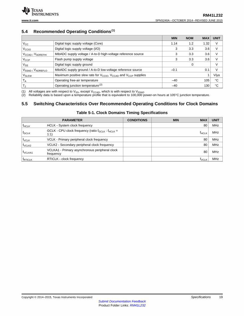
5.4 Recommended Operating Conditions (1)
MIN NOM MAX UNITVCC Digital logic supply voltage (Core) 1.14 1.2 1.32 VVCCIO Digital logic supply voltage (I/O) 3 3.3 3.6 VVCCAD / VADREFHI MibADC supply voltage / A-to-D high-voltage reference source 3 3.3 3.6 VVCCP Flash pump supply voltage 3 3.3 3.6 VVSS Digital logic supply ground 0 VVSSAD / VADREFLO MibADC supply ground / A-to-D low-voltage reference source –0.1 0.1 VVSLEW Maximum positive slew rate for VCCIO, VCCAD and VCCP supplies 1 V/µsTA Operating free-air temperature –40 105 °CTJ Operating junction temperature (2) –40 130 °C
(1) All voltages are with respect to VSS, except VCCAD, which is with respect to VSSAD(2) Reliability data is based upon a temperature profile that is equivalent to 100,000 power-on hours at 105°C junction temperature.
5.5 Switching Characteristics Over Recommended Operating Conditions for Clock Domains
Table 5-1. Clock Domains Timing Specifications
PARAMETER CONDITIONS MIN MAX UNITfHCLK HCLK - System clock frequency 80 MHz
GCLK - CPU clock frequency (ratio fGCLK : fHCLK =fGCLK fHCLK MHz1:1)fVCLK VCLK - Primary peripheral clock frequency 80 MHzfVCLK2 VCLK2 - Secondary peripheral clock frequency 80 MHz
VCLKA1 - Primary asynchronous peripheral clockfVCLKA1 80 MHzfrequencyfRTICLK RTICLK - clock frequency fVCLK MHz
Copyright © 2014–2015, Texas Instruments Incorporated Specifications 19Submit Documentation FeedbackProduct Folder Links: RM41L232
ASWSTEN
Flash Address Wait States
EEPROM Emulation Memory Wait States (Bank 7)
0MHz
080MHz
EWAIT
Main Memory Data Wait States (Bank 0)
RWAIT0MHz 80MHz
0 145MHz
0MHz
280MHz
1 367MHz50MHz
RM41L232SPNS240A –OCTOBER 2014–REVISED JUNE 2015 www.ti.com
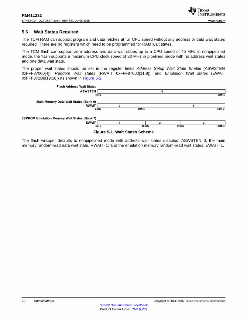
5.6 Wait States RequiredThe TCM RAM can support program and data fetches at full CPU speed without any address or data wait statesrequired. There are no registers which need to be programmed for RAM wait states.
The TCM flash can support zero address and data wait states up to a CPU speed of 45 MHz in nonpipelinedmode.The flash supports a maximum CPU clock speed of 80 MHz in pipelined mode with no address wait statesand one data wait state.
The proper wait states should be set in the register fields Address Setup Wait State Enable (ASWSTEN0xFFF87000[4]), Random Wait states (RWAIT 0xFFF87000[11:8]), and Emulation Wait states (EWAIT0xFFF872B8[19:16]) as shown in Figure 5-1.
Figure 5-1. Wait States Scheme
The flash wrapper defaults to nonpipelined mode with address wait states disabled, ASWSTEN=0; the mainmemory random-read data wait state, RWAIT=1; and the emulation memory random-read wait states, EWAIT=1.
20 Specifications Copyright © 2014–2015, Texas Instruments IncorporatedSubmit Documentation FeedbackProduct Folder Links: RM41L232
RM41L232www.ti.com SPNS240A –OCTOBER 2014–REVISED JUNE 2015
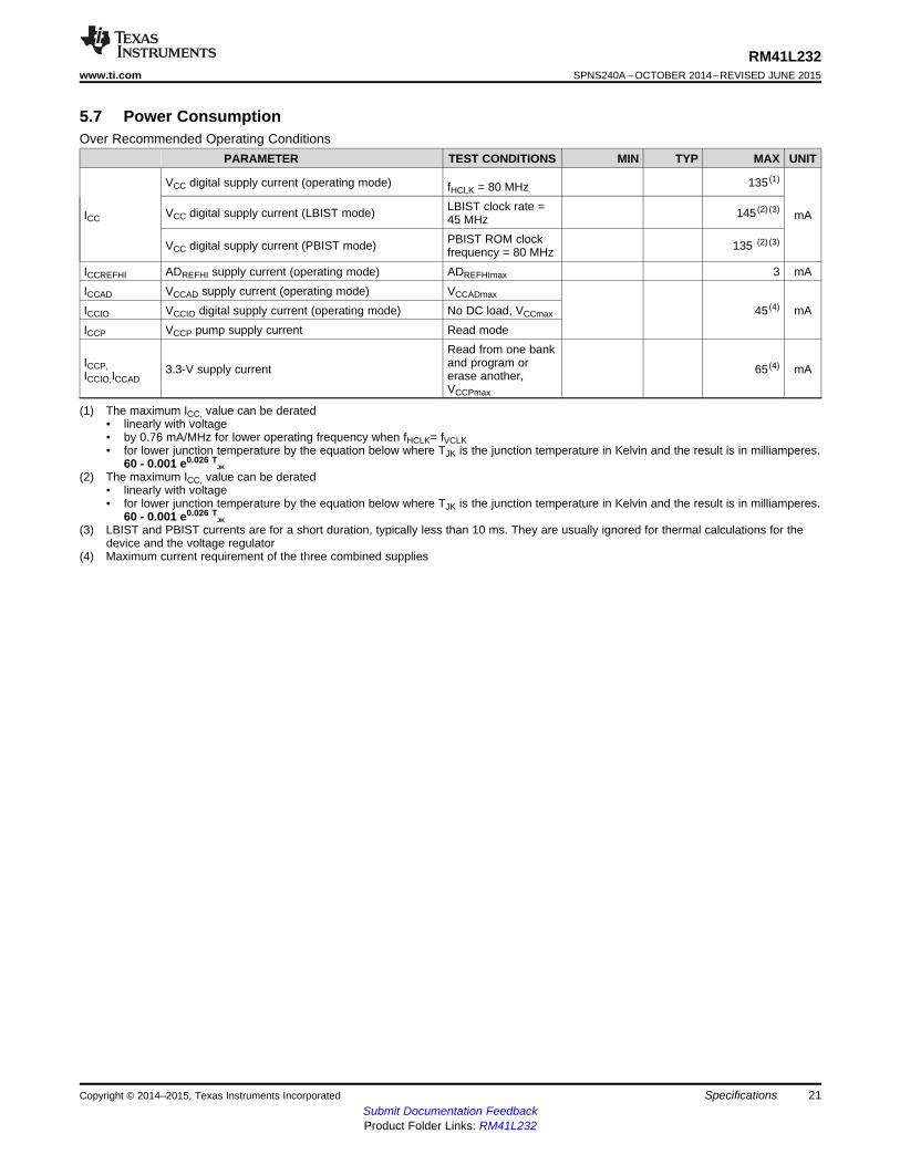
5.7 Power ConsumptionOver Recommended Operating Conditions
PARAMETER TEST CONDITIONS MIN TYP MAX UNIT
VCC digital supply current (operating mode) 135 (1)fHCLK = 80 MHzLBIST clock rate =VCC digital supply current (LBIST mode) 145 (2) (3)ICC mA45 MHzPBIST ROM clockVCC digital supply current (PBIST mode) 135 (2) (3)frequency = 80 MHz
ICCREFHI ADREFHI supply current (operating mode) ADREFHImax 3 mAICCAD VCCAD supply current (operating mode) VCCADmax
ICCIO VCCIO digital supply current (operating mode) No DC load, VCCmax 45 (4) mAICCP VCCP pump supply current Read mode
Read from one bankICCP, and program or3.3-V supply current 65 (4) mAICCIO,ICCAD erase another,
VCCPmax
(1) The maximum ICC, value can be derated• linearly with voltage• by 0.76 mA/MHz for lower operating frequency when fHCLK= fVCLK• for lower junction temperature by the equation below where TJK is the junction temperature in Kelvin and the result is in milliamperes.
60 - 0.001 e0.026 TJK
(2) The maximum ICC, value can be derated• linearly with voltage• for lower junction temperature by the equation below where TJK is the junction temperature in Kelvin and the result is in milliamperes.
60 - 0.001 e0.026 TJK
(3) LBIST and PBIST currents are for a short duration, typically less than 10 ms. They are usually ignored for thermal calculations for thedevice and the voltage regulator
(4) Maximum current requirement of the three combined supplies
Copyright © 2014–2015, Texas Instruments Incorporated Specifications 21Submit Documentation FeedbackProduct Folder Links: RM41L232

RM41L232SPNS240A –OCTOBER 2014–REVISED JUNE 2015 www.ti.com
5.8 Thermal Resistance Characteristics for PZTable 5-2 shows the thermal resistance characteristics for the PQFP - PZ mechanical packages.
Table 5-2. Thermal Resistance Characteristics(S-PQFP Package) [PZ]
PARAMETER °C/WRθJA 48RθJC 5
5.9 Input/Output Electrical Characteristics (1)
Over Recommended Operating ConditionsPARAMETER TEST CONDITIONS MIN TYP MAX UNIT
Vhys Input hysteresis All inputs 180 mVVIL Low-level input voltage All inputs (2) –0.3 0.8 VVIH High-level input voltage All inputs (2) 2 VCCIO + 0.3 V
IOL = IOLmax 0.2 VCCIO
IOL = 50 µA,VOL Low-level output voltage Vstandard output 0.2modeIOH = IOHmax 0.8 VCCIO
IOH = 50 µA,VOH High-level output voltage Vstandard output VCCIO - 0.3modeVI < VSSIO - 0.3 or VIIIC Input clamp current (I/O pins) –3.5 3.5 mA> VCCIO + 0.3
IIH 20-µA pulldown VI = VCCIO 5 40IIH 100-µA pulldown VI = VCCIO 40 195IIL 20-µA pullup VI = VSS –40 –5II Input current (I/O pins) µAIIL 100-µA pullup VI = VSS –195 –40
No pullup orAll other pins –1 1pulldownCI Input capacitance 2 pFCO Output capacitance 3 pF
(1) Source currents (out of the device) are negative while sink currents (into the device) are positive.(2) This does not apply to the nPORRST pin.
22 Specifications Copyright © 2014–2015, Texas Instruments IncorporatedSubmit Documentation FeedbackProduct Folder Links: RM41L232

RM41L232www.ti.com SPNS240A –OCTOBER 2014–REVISED JUNE 2015
5.10 Output Buffer Drive Strengths
Table 5-3. Output Buffer Drive Strengths
LOW-LEVEL OUTPUT CURRENT,IOL for VI=VOLmax
or SIGNALSHIGH-LEVEL OUTPUT CURRENT,
IOH for VI=VOHmin
EQEPI, EQEPS,8 mA TMS, TDI, TDO, RTCK,
nERROR
TEST,4 mA MIBSPI1SIMO, MIBSPI1SOMI, MIBSPI1CLK, SPI3CLK, SPI3SIMO, SPI3SOMI,
nRST
AD1EVT,
CAN1RX, CAN1TX, CAN2RX, CAN2TX,
GIOA[0-7],
LINRX, LINTX,2 mA zero-dominant
MIBSPI1nCS[0-3], MIBSPI1nENA
N2HET[0], N2HET[2], N2HET[4], N2HET[6], N2HET[8], N2HET[10], N2HET[12], N2HET[14],N2HET[16], N2HET[18], N2HET[22], N2HET[24],
SPI2nCS[0-3], SPI3nENA, SPI3nCS[0]
ECLK,selectable 8 mA/ 2 mA SPI2CLK, SPI2SIMO, SPI2SOMI
The default output buffer drive strength is 8 mA for these signals.
Table 5-4. Selectable 8 mA/ 2 mA Control
SIGNAL CONTROL BIT ADDRESS 8 mA 2 mAECLK SYSPC10[0] 0xFFFF FF78 0 1
SPI2CLK SPI2PC9[9] 0xFFF7 F668 0 1SPI2SIMO SPI2PC9[10] 0xFFF7 F668 0 1SPI2SOMI SPI2PC9[11] (1) 0xFFF7 F668 0 1
(1) Either SPI2PC9[11] or SPI2PC9[24] can change the output strength of the SPI2SOMI pin. In case of a 32-bit write where these 2 bitsdiffer, SPI2PC9[11] determines the drive strength.
Copyright © 2014–2015, Texas Instruments Incorporated Specifications 23Submit Documentation FeedbackProduct Folder Links: RM41L232

VCCIO
V IHVIH
VIL0
Input
tpw
V IL
RM41L232SPNS240A –OCTOBER 2014–REVISED JUNE 2015 www.ti.com
5.11 Input Timings
Figure 5-2. TTL-Level Inputs
Table 5-5. Timing Requirements for Inputs (1)
MIN MAX UNITtpw Input minimum pulse width tc(VCLK) + 10 (2) ns
(1) tc(VCLK) = peripheral VBUS clock cycle time = 1 / f(VCLK)(2) The timing shown in Figure 5-2 is only valid for pin used in GIO mode.
24 Specifications Copyright © 2014–2015, Texas Instruments IncorporatedSubmit Documentation FeedbackProduct Folder Links: RM41L232
RM41L232www.ti.com SPNS240A –OCTOBER 2014–REVISED JUNE 2015
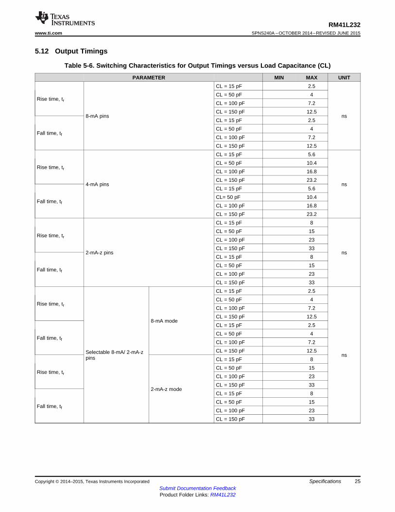
5.12 Output Timings
Table 5-6. Switching Characteristics for Output Timings versus Load Capacitance (CL)
PARAMETER MIN MAX UNITCL = 15 pF 2.5CL = 50 pF 4
Rise time, tr CL = 100 pF 7.2CL = 150 pF 12.5
8-mA pins nsCL = 15 pF 2.5CL = 50 pF 4
Fall time, tf CL = 100 pF 7.2CL = 150 pF 12.5CL = 15 pF 5.6CL = 50 pF 10.4
Rise time, tr CL = 100 pF 16.8CL = 150 pF 23.2
4-mA pins nsCL = 15 pF 5.6CL= 50 pF 10.4
Fall time, tf CL = 100 pF 16.8CL = 150 pF 23.2CL = 15 pF 8CL = 50 pF 15
Rise time, tr CL = 100 pF 23CL = 150 pF 33
2-mA-z pins nsCL = 15 pF 8CL = 50 pF 15
Fall time, tf CL = 100 pF 23CL = 150 pF 33CL = 15 pF 2.5CL = 50 pF 4
Rise time, tr CL = 100 pF 7.2CL = 150 pF 12.5
8-mA modeCL = 15 pF 2.5CL = 50 pF 4
Fall time, tf CL = 100 pF 7.2CL = 150 pF 12.5Selectable 8-mA/ 2-mA-z nspins CL = 15 pF 8CL = 50 pF 15
Rise time, tr CL = 100 pF 23CL = 150 pF 33
2-mA-z modeCL = 15 pF 8CL = 50 pF 15
Fall time, tf CL = 100 pF 23CL = 150 pF 33
Copyright © 2014–2015, Texas Instruments Incorporated Specifications 25Submit Documentation FeedbackProduct Folder Links: RM41L232
tftr
VCCIOVOH VOH
VOL VOL0
Output
RM41L232SPNS240A –OCTOBER 2014–REVISED JUNE 2015 www.ti.com
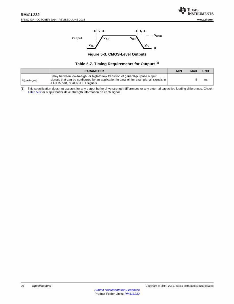
Figure 5-3. CMOS-Level Outputs
Table 5-7. Timing Requirements for Outputs (1)
PARAMETER MIN MAX UNITDelay between low-to-high, or high-to-low transition of general-purpose output
td(parallel_out) signals that can be configured by an application in parallel, for example, all signals in 5 nsa GIOA port, or all N2HET signals.
(1) This specification does not account for any output buffer drive strength differences or any external capacitive loading differences. CheckTable 5-3 for output buffer drive strength information on each signal.
26 Specifications Copyright © 2014–2015, Texas Instruments IncorporatedSubmit Documentation FeedbackProduct Folder Links: RM41L232

RM41L232www.ti.com SPNS240A –OCTOBER 2014–REVISED JUNE 2015
6 System Information and Electrical Specifications
6.1 Voltage Monitor CharacteristicsA voltage monitor is implemented on this device. The purpose of this voltage monitor is to eliminate therequirement for a specific sequence when powering up the core and I/O voltage supplies.
6.1.1 Important Considerations• The voltage monitor does not eliminate the need of a voltage supervisor circuit to ensure that the
device is held in reset when the voltage supplies are out of range.• The voltage monitor only monitors the core supply (VCC) and the I/O supply (VCCIO). The other
supplies are not monitored by the VMON. For example, if the VCCAD or VCCP are supplied from asource different from that for VCCIO, then there is no internal voltage monitor for the VCCAD andVCCP supplies.
6.1.2 Voltage Monitor OperationThe voltage monitor generates the Power Good MCU signal (PGMCU) as well as the I/Os Power GoodI/O signal (PGIO) on the device. During power up or power down, the PGMCU and PGIO are driven lowwhen the core or I/O supplies are lower than the specified minimum monitoring thresholds. The PGIO andPGMCU being low isolates the core logic as well as the I/O controls during the power up or power down ofthe supplies. This allows the core and I/O supplies to be powered up or down in any order.
When the voltage monitor detects a low voltage on the I/O supply, it will assert a power-on reset. Whenthe voltage monitor detects an out-of-range voltage on the core supply, it asynchronously makes all outputpins high impedance, and asserts a power-on reset. The voltage monitor is disabled when the deviceenters a low power mode.
The VMON also incorporates a glitch filter for the nPORRST input. Refer to Section 6.2.3.1 for the timinginformation on this glitch filter.
Table 6-1. Voltage Monitoring Specifications
PARAMETER MIN TYP MAX UNITVCC low - VCC level below this 0.75 0.9 1.13threshold is detected as too low.VCC high - VCC level above thisVoltage monitoring 1.40 1.7 2.1VMON threshold is detected as too high. VthresholdsVCCIO low - VCCIO level belowthis threshold is detected as too 1.85 2.4 2.9low.
6.1.3 Supply FilteringThe VMON has the capability to filter glitches on the VCC and VCCIO supplies.
Table 6-2 shows the characteristics of the supply filtering. Glitches in the supply larger than the maximumspecification cannot be filtered.
Table 6-2. VMON Supply Glitch Filtering Capability
PARAMETER MIN MAX UNITWidth of glitch on VCC that can be filtered 250 1000 nsWidth of glitch on VCCIO that can be filtered 250 1000 ns
Copyright © 2014–2015, Texas Instruments Incorporated System Information and Electrical Specifications 27Submit Documentation FeedbackProduct Folder Links: RM41L232
RM41L232SPNS240A –OCTOBER 2014–REVISED JUNE 2015 www.ti.com
6.2 Power Sequencing and Power-On Reset
6.2.1 Power-Up SequenceThere is no timing dependency between the ramp of the VCCIO and the VCC supply voltage. The power-up sequence starts with the I/O voltage rising above the minimum I/O supply threshold, (for more details,see Table 6-4), core voltage rising above the minimum core supply threshold, and the release of power-onreset. The high-frequency oscillator will start up first and its amplitude will grow to an acceptable level. Theoscillator start-up time is dependent on the type of oscillator and is provided by the oscillator vendor. Thedifferent supplies to the device can be powered up in any order.
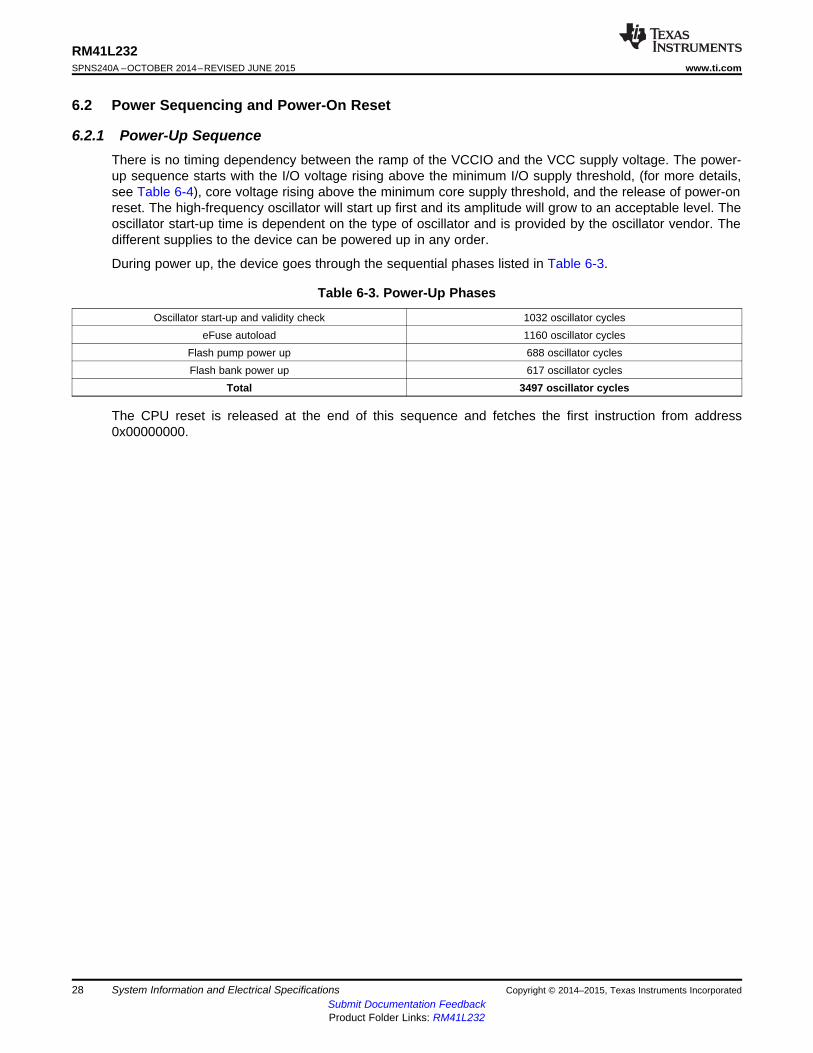
During power up, the device goes through the sequential phases listed in Table 6-3.
Table 6-3. Power-Up Phases
Oscillator start-up and validity check 1032 oscillator cycleseFuse autoload 1160 oscillator cycles
Flash pump power up 688 oscillator cyclesFlash bank power up 617 oscillator cycles
Total 3497 oscillator cycles
The CPU reset is released at the end of this sequence and fetches the first instruction from address0x00000000.
28 System Information and Electrical Specifications Copyright © 2014–2015, Texas Instruments IncorporatedSubmit Documentation FeedbackProduct Folder Links: RM41L232

3.3 VVCCIOPORH
1.2 VVCCPORH
VCCIOPORL
V (1.2 V)
V / V (3.3 V)CC
CCIO CCP
nPORRST
8
66
7
7
93
VCCPORL
VIL(PORRST)
V / VCCIO CCP
VCC
VCCPORL
VIL(PORRST)VIL VIL VIL
VCCIOPORH
VCCPORH
VCCIOPORL
NOTE: There is no timing dependency between the ramp of the VCCIO and the VCC supply voltage; this is just an exemplary drawing.
RM41L232www.ti.com SPNS240A –OCTOBER 2014–REVISED JUNE 2015
6.2.2 Power-Down SequenceThe different supplies to the device can be powered down in any order.
6.2.3 Power-On Reset: nPORRSTThis reset must be asserted by an external circuitry whenever the I/O or core supplies are outside therecommended range. This signal has a glitch filter on it. It also has an internal pulldown.
6.2.3.1 nPORRST Electrical and Timing Requirements
Table 6-4. Electrical Requirements for nPORRST
NO. PARAMETER MIN MAX UNITVCC low supply level when nPORRST must be active during powerVCCPORL 0.5 VupVCC high supply level when nPORRST must remain active duringVCCPORH 1.14 Vpower up and become active during power downVCCIO / VCCP low supply level when nPORRST must be activeVCCIOPORL 1.1 Vduring power upVCCIO / VCCP high supply level when nPORRST must remain activeVCCIOPORH 3.0 Vduring power up and become active during power down
VIL(PORRST) Low-level input voltage of nPORRST VCCIO > 2.5 V 0.2 * VCCIO VLow-level input voltage of nPORRST VCCIO < 2.5 V 0.5 VSetup time, nPORRST active before VCCIO and VCCP > VCCIOPORL3 tsu(PORRST) 0 msduring power up
6 th(PORRST) Hold time, nPORRST active after VCC > VCCPORH 1 msSetup time, nPORRST active before VCC < VCCPORH during power7 tsu(PORRST) 2 µsdown
8 th(PORRST) Hold time, nPORRST active after VCCIO and VCCP > VCCIOPORH 1 ms9 th(PORRST) Hold time, nPORRST active after VCC < VCCPORL 0 ms
Filter time nPORRST pin;tf(nPORRST) Pulses less than MIN will be filtered out, pulses greater than MAX 475 2000 ns
will generate a reset.
Figure 6-1. nPORRST Timing Diagram
Copyright © 2014–2015, Texas Instruments Incorporated System Information and Electrical Specifications 29Submit Documentation FeedbackProduct Folder Links: RM41L232
RM41L232SPNS240A –OCTOBER 2014–REVISED JUNE 2015 www.ti.com
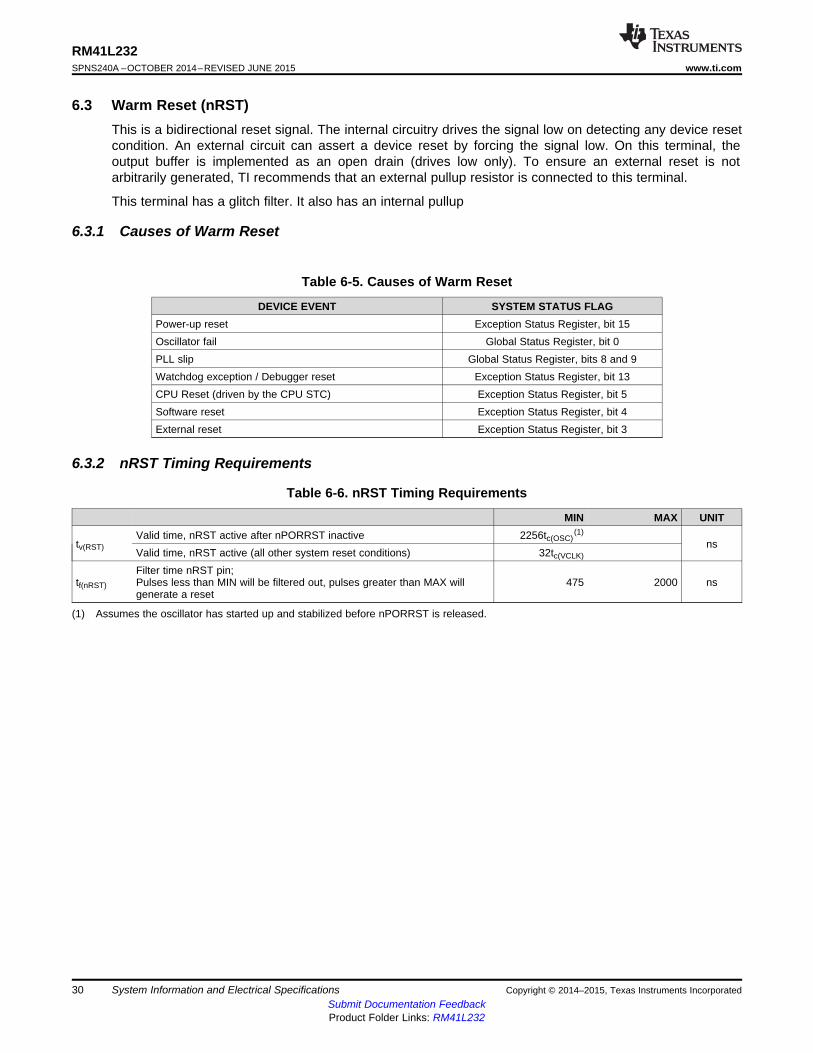
6.3 Warm Reset (nRST)This is a bidirectional reset signal. The internal circuitry drives the signal low on detecting any device resetcondition. An external circuit can assert a device reset by forcing the signal low. On this terminal, theoutput buffer is implemented as an open drain (drives low only). To ensure an external reset is notarbitrarily generated, TI recommends that an external pullup resistor is connected to this terminal.
This terminal has a glitch filter. It also has an internal pullup
6.3.1 Causes of Warm Reset
Table 6-5. Causes of Warm Reset
DEVICE EVENT SYSTEM STATUS FLAGPower-up reset Exception Status Register, bit 15Oscillator fail Global Status Register, bit 0PLL slip Global Status Register, bits 8 and 9Watchdog exception / Debugger reset Exception Status Register, bit 13CPU Reset (driven by the CPU STC) Exception Status Register, bit 5Software reset Exception Status Register, bit 4External reset Exception Status Register, bit 3
6.3.2 nRST Timing Requirements
Table 6-6. nRST Timing Requirements
MIN MAX UNITValid time, nRST active after nPORRST inactive 2256tc(OSC)
(1)tv(RST) ns
Valid time, nRST active (all other system reset conditions) 32tc(VCLK)
Filter time nRST pin;tf(nRST) Pulses less than MIN will be filtered out, pulses greater than MAX will 475 2000 ns
generate a reset
(1) Assumes the oscillator has started up and stabilized before nPORRST is released.
30 System Information and Electrical Specifications Copyright © 2014–2015, Texas Instruments IncorporatedSubmit Documentation FeedbackProduct Folder Links: RM41L232

North Flip West
FF
RM41L232www.ti.com SPNS240A –OCTOBER 2014–REVISED JUNE 2015
6.4 ARM Cortex-R4 CPU Information
6.4.1 Summary of ARM Cortex-R4 CPU FeaturesThe features of the ARM Cortex-R4 CPU include:• An integer unit with integral Embedded ICE-RT logic.• High-speed Advanced Microprocessor Bus Architecture (AMBA) Advanced eXtensible Interfaces (AXI)
for Level two (L2) master and slave interfaces.• Dynamic branch prediction with a global history buffer, and a 4-entry return stack• Low interrupt latency.• Nonmaskable interrupt.• A Harvard Level one (L1) memory system with:
– Tightly Coupled Memory (TCM) interfaces with support for error correction or parity checkingmemories
– ARMv7-R architecture Memory Protection Unit (MPU) with 8 regions• Dual core logic for fault detection in safety-critical applications.• An L2 memory interface:
– Single 64-bit master AXI interface– 64-bit slave AXI interface to TCM RAM blocks
• A debug interface to a CoreSight Debug Access Port (DAP).• Six Hardware Breakpoints• Two Watchpoints• A Perfomance Monitoring Unit (PMU)• A Vectored Interrupt Controller (VIC) port.
For more information on the ARM Cortex-R4 CPU, see www.arm.com.
6.4.2 ARM Cortex-R4 CPU Features Enabled by SoftwareThe following CPU features are disabled on reset and must be enabled by the application if required.• ECC On Tightly Coupled Memory (TCM) Accesses• Hardware Vectored Interrupt (VIC) Port• Memory Protection Unit (MPU)
6.4.3 Dual Core ImplementationThe device has two Cortex-R4 cores, where the output signals of both CPUs are compared in the CCM-R4 unit. To avoid common mode impacts the signals of the CPUs to be compared are delayed by 2 clockcycles as shown in Figure 6-3.
The CPUs have a diverse CPU placement given by following requirements:• Different orientation; for example, CPU1 = "north" orientation, CPU2 = "flip west" orientation• Dedicated guard ring for each CPU
Figure 6-2. Dual - CPU Orientation
Copyright © 2014–2015, Texas Instruments Incorporated System Information and Electrical Specifications 31Submit Documentation FeedbackProduct Folder Links: RM41L232

CPU 1 CPU 2
2 cycle delay
2 cycle delay
CCM-R4
CCM-R4
compareCPU1CLK
CPU2CLK
compareerror
Input + Control
Output + Control
RM41L232SPNS240A –OCTOBER 2014–REVISED JUNE 2015 www.ti.com
6.4.4 Duplicate clock tree after GCLKThe CPU clock domain is split into two clock trees, one for each CPU, with the clock of the 2nd CPUrunning at the same frequency and in phase to the clock of CPU1. See Figure 6-3.
6.4.5 ARM Cortex-R4 CPU Compare Module (CCM) for SafetyThis device has two ARM Cortex-R4 CPU cores, where the output signals of both CPUs are compared inthe CCM-R4 unit. To avoid common mode impacts the signals of the CPUs to be compared are delayed ina different way as shown in Figure 6-3.
Figure 6-3. Dual Core Implementation
To avoid an erroneous CCM-R4 compare error, the application software must initialize the registers ofboth CPUs before the registers are used, including function calls where the register values are pushedonto the stack.
6.4.6 CPU Self-TestThe CPU STC (Self-Test Controller) is used to test the two Cortex-R4 CPU Cores using the DeterministicLogic BIST Controller as the test engine.
The main features of the self-test controller are:• Ability to divide the complete test run into independent test intervals• Capable of running the complete test or running a few intervals at a time• Ability to continue from the last executed interval (test set) or to restart from the beginning (first test
set)• Complete isolation of the self-tested CPU core from the rest of the system during the self-test run• Ability to capture the failure interval number• Timeout counter for the CPU self-test run as a fail-safe feature
32 System Information and Electrical Specifications Copyright © 2014–2015, Texas Instruments IncorporatedSubmit Documentation FeedbackProduct Folder Links: RM41L232

RM41L232www.ti.com SPNS240A –OCTOBER 2014–REVISED JUNE 2015
6.4.6.1 Application Sequence for CPU Self-Test
1. Configure clock domain frequencies.2. Select the number of test intervals to be run.3. Configure the timeout period for the self-test run.4. Save the CPU state if required5. Enable self-test.6. Wait for CPU reset.7. In the reset handler, read CPU self-test status to identify any failures.8. Retrieve CPU state if required.
For more information, see the RM41x 16/32-Bit RISC Flash Microcontroller Technical Reference Manual(SPNU596).
6.4.6.2 CPU Self-Test Clock Configuration
The maximum clock rate for the self-test is 45 MHz. The STCCLK is divided down from the CPU clock,when necessary. This divider is configured by the STCCLKDIV register at address 0xFFFFE108.
6.4.6.3 CPU Self-Test Coverage
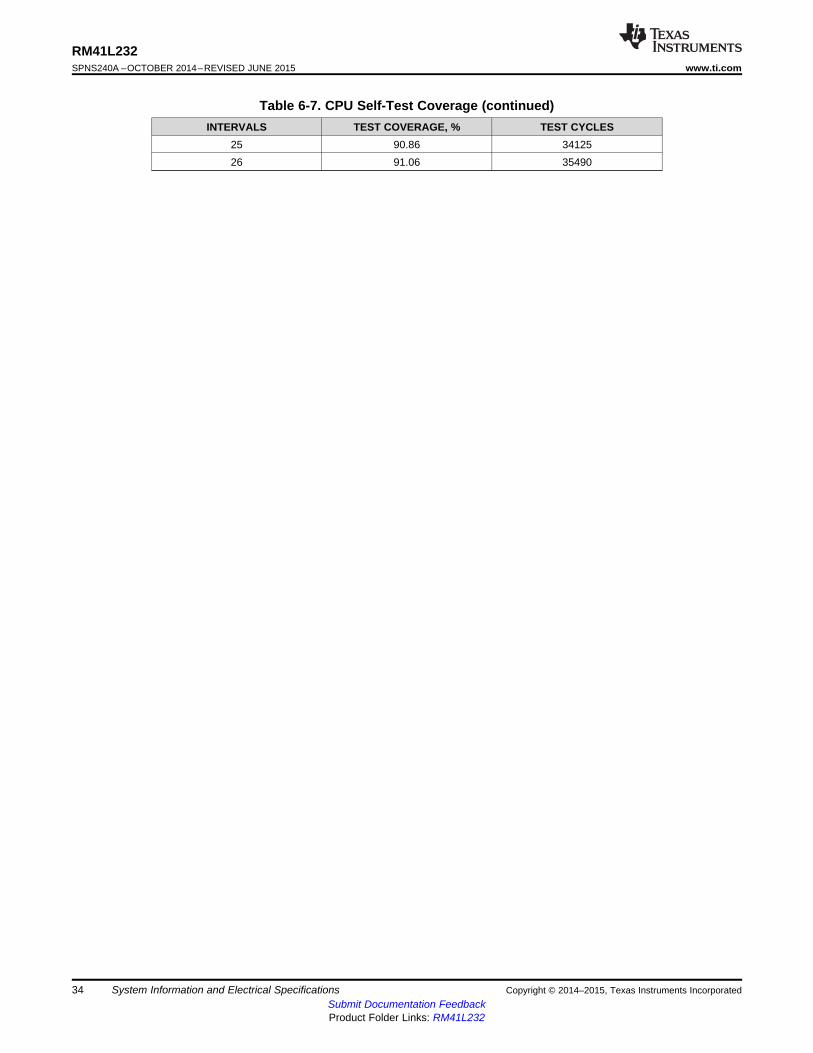
Table 6-7 shows CPU test coverage achieved for each self-test interval. It also lists the cumulative testcycles. The test time can be calculated by multiplying the number of test cycles with the STC clock period.
Table 6-7. CPU Self-Test Coverage
INTERVALS TEST COVERAGE, % TEST CYCLES0 0 01 60.06 13652 68.71 27303 73.35 40954 76.57 54605 78.7 68256 80.4 81907 81.76 95558 82.94 109209 83.84 1228510 84.58 1365011 85.31 1501512 85.9 1638013 86.59 1774514 87.17 1911015 87.67 2047516 88.11 2184017 88.53 2320518 88.93 2457019 89.26 2593520 89.56 2730021 89.86 2866522 90.1 3003023 90.36 3139524 90.62 32760
Copyright © 2014–2015, Texas Instruments Incorporated System Information and Electrical Specifications 33Submit Documentation FeedbackProduct Folder Links: RM41L232
RM41L232SPNS240A –OCTOBER 2014–REVISED JUNE 2015 www.ti.com
Table 6-7. CPU Self-Test Coverage (continued)INTERVALS TEST COVERAGE, % TEST CYCLES
25 90.86 3412526 91.06 35490
34 System Information and Electrical Specifications Copyright © 2014–2015, Texas Instruments IncorporatedSubmit Documentation FeedbackProduct Folder Links: RM41L232

OSCIN OSCOUT
C1
(see Note A)
C2
Crystal
(a)
OSCIN OSCOUT
(b)
External
(toggling 0 V to 3.3 V)Clock Signal
Note A: The values of C1 and C2 should be provided by the resonator/crystal vendor.
Kelvin_GND
Note B: Kelvin_GND should not be connected to any other GND.
(see Note B)
RM41L232www.ti.com SPNS240A –OCTOBER 2014–REVISED JUNE 2015
6.5 Clocks
6.5.1 Clock SourcesThe table below lists the available clock sources on the device. Each of the clock sources can be enabledor disabled using the CSDISx registers in the system module. The clock source number in the tablecorresponds to the control bit in the CSDISx register for that clock source.
The table also shows the default state of each clock source.
Table 6-8. Available Clock Sources
CLOCKSOURCE NAME DESCRIPTION DEFAULT STATE
NO.0 OSCIN Main Oscillator Enabled1 PLL1 Output From PLL1 Disabled2 Reserved Reserved Disabled3 EXTCLKIN1 External Clock Input #1 Disabled4 CLK80K Low-Frequency Output of Internal Reference Oscillator Enabled5 CLK10M High-Frequency Output of Internal Reference Oscillator Enabled6 Reserved Reserved Disabled7 Reserved Reserved Disabled
6.5.1.1 Main Oscillator
The oscillator is enabled by connecting the appropriate fundamental resonator/crystal and load capacitorsacross the external OSCIN and OSCOUT pins as shown in Figure 6-4. The oscillator is a single stageinverter held in bias by an integrated bias resistor. This resistor is disabled during leakage testmeasurement and low power modes.
TI strongly encourages each customer to submit samples of the device to the resonator/crystalvendors for validation. The vendors are equipped to determine what load capacitors will best tunetheir resonator/crystal to the microcontroller device for optimum start-up and operation overtemperature/voltage extremes.
An external oscillator source can be used by connecting a 3.3 V clock signal to the OSCIN pin and leavingthe OSCOUT pin unconnected (open) as shown in Figure 6-4.
Figure 6-4. Recommended Crystal/Clock Connection
Copyright © 2014–2015, Texas Instruments Incorporated System Information and Electrical Specifications 35Submit Documentation FeedbackProduct Folder Links: RM41L232
BIAS_EN
Low-PowerOscillator
LFEN
LF_TRIM
HFEN
HF_TRIM
CLK80K
CLK10M
CLK10M_VALID
nPORRST
RM41L232SPNS240A –OCTOBER 2014–REVISED JUNE 2015 www.ti.com
6.5.1.1.1 Timing Requirements for Main Oscillator
Table 6-9. Timing Requirements for Main Oscillator
PARAMETER MIN TYP MAX UNITtc(OSC) Cycle time, OSCIN (when using a sine-wave input) 50 200 nstc(OSC_SQR) Cycle time, OSCIN, (when input to the OSCIN is a square 50 200 nswave )tw(OSCIL) Pulse duration, OSCIN low (when input to the OSCIN is a 15 nssquare wave)tw(OSCIH) Pulse duration, OSCIN high (when input to the OSCIN is a 15 nssquare wave)
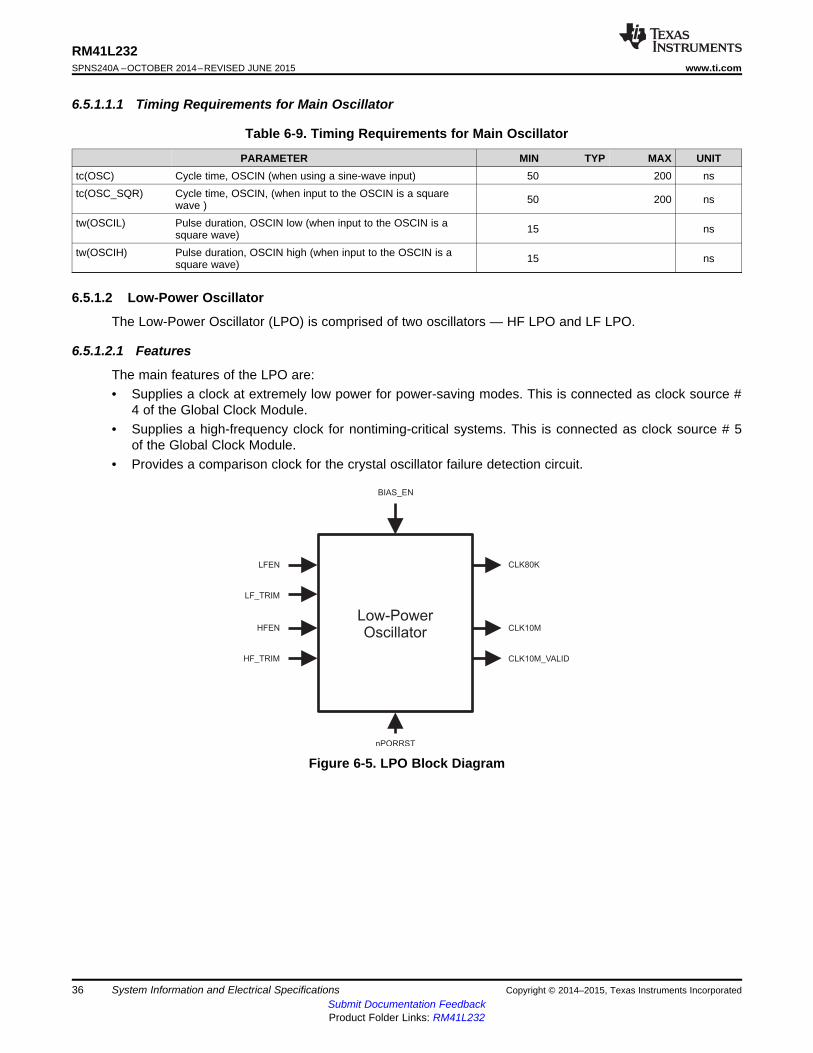
6.5.1.2 Low-Power Oscillator
The Low-Power Oscillator (LPO) is comprised of two oscillators — HF LPO and LF LPO.
6.5.1.2.1 Features
The main features of the LPO are:• Supplies a clock at extremely low power for power-saving modes. This is connected as clock source #
4 of the Global Clock Module.• Supplies a high-frequency clock for nontiming-critical systems. This is connected as clock source # 5
of the Global Clock Module.• Provides a comparison clock for the crystal oscillator failure detection circuit.
Figure 6-5. LPO Block Diagram
36 System Information and Electrical Specifications Copyright © 2014–2015, Texas Instruments IncorporatedSubmit Documentation FeedbackProduct Folder Links: RM41L232
/NR
/1 to /64
OSCIN
PLL
INTCLK /OD
/1 to /8
VCOCLK /R
/1 to /32
post_ODCLK
/NF
/1 to /256
PLLCLK
fPLLCLK = (fOSCIN / NR) * NF / (OD * R)
RM41L232www.ti.com SPNS240A –OCTOBER 2014–REVISED JUNE 2015
Figure 6-5 shows a block diagram of the internal reference oscillator. This is an LPO and provides twoclock sources: one nominally 80 kHz and one nominally 10 MHz.
6.5.1.2.2 LPO Electrical and Timing Specifications
Table 6-10. LPO Specifications
PARAMETER MIN TYP MAX UNITOscillator fail frequency - lower threshold, using 1.375 2.4 4.875untrimmed LPO output
Clock Detection MHzOscillator fail frequency - higher threshold, using 22 38.4 78untrimmed LPO outputUntrimmed frequency 5.5 9 19.5 MHzTrimmed frequency 8 9.6 11 MHz
LPO - HF oscillatorStart-up time from STANDBY (LPO BIAS_EN High for(fHFLPO) 10 µsat least 900 µs)Cold start-up time 900 µsUntrimmed frequency 36 85 180 kHz
LPO - LF oscillator Start-up time from STANDBY (LPO BIAS_EN High for 100 µs(fLFLPO) at least 900 µs)Cold start-up time 2000 µs
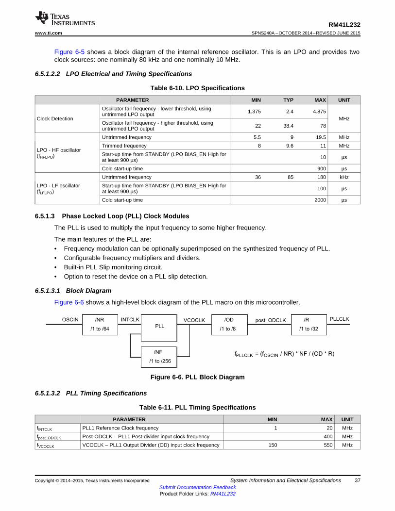
6.5.1.3 Phase Locked Loop (PLL) Clock Modules
The PLL is used to multiply the input frequency to some higher frequency.
The main features of the PLL are:• Frequency modulation can be optionally superimposed on the synthesized frequency of PLL.• Configurable frequency multipliers and dividers.• Built-in PLL Slip monitoring circuit.• Option to reset the device on a PLL slip detection.
6.5.1.3.1 Block Diagram
Figure 6-6 shows a high-level block diagram of the PLL macro on this microcontroller.
Figure 6-6. PLL Block Diagram
6.5.1.3.2 PLL Timing Specifications
Table 6-11. PLL Timing Specifications
PARAMETER MIN MAX UNITfINTCLK PLL1 Reference Clock frequency 1 20 MHzfpost_ODCLK Post-ODCLK – PLL1 Post-divider input clock frequency 400 MHzfVCOCLK VCOCLK – PLL1 Output Divider (OD) input clock frequency 150 550 MHz
Copyright © 2014–2015, Texas Instruments Incorporated System Information and Electrical Specifications 37Submit Documentation FeedbackProduct Folder Links: RM41L232

RM41L232SPNS240A –OCTOBER 2014–REVISED JUNE 2015 www.ti.com
6.5.2 Clock Domains
6.5.2.1 Clock Domain Descriptions
Table 6-12 lists the device clock domains and their default clock sources. The table also shows thesystem module control register that is used to select an available clock source for each clock domain.
Table 6-12. Clock Domain Descriptions
CLOCK SOURCECLOCK DOMAIN DEFAULT CLOCK SELECTION DESCRIPTIONNAME SOURCE REGISTER
HCLK OSCIN GHVSRC • Is disabled through the CDDISx registers bit 1
• Always the same frequency as HCLK• In phase with HCLK• Is disabled separately from HCLK through the CDDISx registers
GCLK OSCIN GHVSRC bit 0• Can be divided by 1 up to 8 when running CPU self-test
(LBIST) using the CLKDIV field of the STCCLKDIV register ataddress 0xFFFFE108
• Always the same frequency as GCLK• 2 cycles delayed from GCLK
GCLK2 OSCIN GHVSRC • Is disabled along with GCLK• Gets divided by the same divider setting as that for GCLK when
running CPU self-test (LBIST)
• Divided down from HCLK• Can be HCLK/1, HCLK/2, ... or HCLK/16• Is disabled separately from HCLK through the CDDISx registersVCLK OSCIN GHVSRC
bit 2• Can be disabled separately for eQEP using CDDISx registers
bit 9
• Divided down from HCLK• Can be HCLK/1, HCLK/2, ... or HCLK/16
VCLK2 OSCIN GHVSRC • Frequency must be an integer multiple of VCLK frequency• Is disabled separately from HCLK through the CDDISx registers
bit 3
• Defaults to VCLK as the sourceVCLKA1 VCLK VCLKASRC • Frequency can be as fast as HCLK frequency
• Is disabled through the CDDISx registers bit 4
• Defaults to VCLK as the source• If a clock source other than VCLK is selected for RTICLK, then
the RTICLK frequency must be less than or equal to VCLK/3RTICLK VCLK RCLKSRC– Application can ensure this by programming the RTI1DIV
field of the RCLKSRC register, if necessary• Is disabled through the CDDISx registers bit 6
38 System Information and Electrical Specifications Copyright © 2014–2015, Texas Instruments IncorporatedSubmit Documentation FeedbackProduct Folder Links: RM41L232
/1,2 ...1024
Phase_seg1
CAN Baud Rate
DCAN1, 2
AVCLK1 VCLK
Prop_segPhase_
seg2
/1,2 ...256
SPIBaud Rate
SPIx,MibSPIx
/2,3 ...224
LINBaud Rate
LIN
ADCLK
MibADC
/1,2 ...32
ECLK
External Clock
/1,2 ...65536
VCLK2
HET TU
HRP/1 ...64
N2HET
HighResolution
LoopClock
LRP/20...27
VCLK2
Low PowerOscillator
*The frequency at this node must not exceed the maximum HCLK frequency
*FMzPLL
80 kHz
10 MHz
OSCIN
GCM
0
1
4
5
/1 ...64 X1 ...256 /1 ...8 /1 ...32
GCLK,GCLK2 (to CPU)
HCLK (to SYSTEM)
VCLK (to System and Peripheral Modules)
VCLK (to N2HET)
/1 ...16
/1 ...16
AVCLK1 (to DCAN1, 2)
0
1
4
5
VCLK
VCLK
0
1
4
5
/1,2,4, or 8
RTICLK (to RTI+DWWD)
EXTCLKIN 3
3
3
eQEP
CDDISx.9
RM41L232www.ti.com SPNS240A –OCTOBER 2014–REVISED JUNE 2015
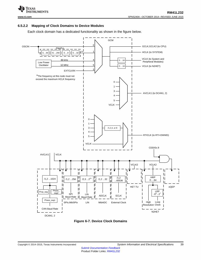
6.5.2.2 Mapping of Clock Domains to Device Modules
Each clock domain has a dedicated functionality as shown in the figure below.
Figure 6-7. Device Clock Domains
Copyright © 2014–2015, Texas Instruments Incorporated System Information and Electrical Specifications 39Submit Documentation FeedbackProduct Folder Links: RM41L232
RM41L232SPNS240A –OCTOBER 2014–REVISED JUNE 2015 www.ti.com
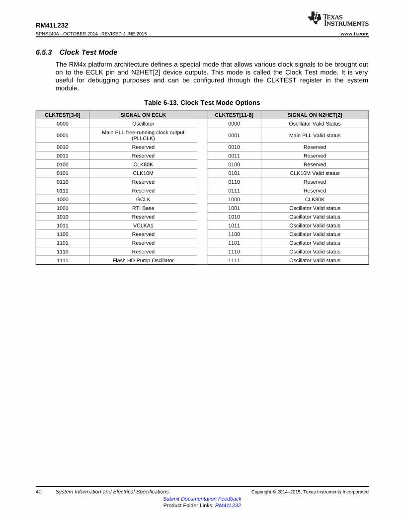
6.5.3 Clock Test ModeThe RM4x platform architecture defines a special mode that allows various clock signals to be brought outon to the ECLK pin and N2HET[2] device outputs. This mode is called the Clock Test mode. It is veryuseful for debugging purposes and can be configured through the CLKTEST register in the systemmodule.
Table 6-13. Clock Test Mode Options
CLKTEST[3-0] SIGNAL ON ECLK CLKTEST[11-8] SIGNAL ON N2HET[2]0000 Oscillator 0000 Oscillator Valid Status
Main PLL free-running clock output0001 0001 Main PLL Valid status(PLLCLK)0010 Reserved 0010 Reserved0011 Reserved 0011 Reserved0100 CLK80K 0100 Reserved0101 CLK10M 0101 CLK10M Valid status0110 Reserved 0110 Reserved0111 Reserved 0111 Reserved1000 GCLK 1000 CLK80K1001 RTI Base 1001 Oscillator Valid status1010 Reserved 1010 Oscillator Valid status1011 VCLKA1 1011 Oscillator Valid status1100 Reserved 1100 Oscillator Valid status1101 Reserved 1101 Oscillator Valid status1110 Reserved 1110 Oscillator Valid status1111 Flash HD Pump Oscillator 1111 Oscillator Valid status
40 System Information and Electrical Specifications Copyright © 2014–2015, Texas Instruments IncorporatedSubmit Documentation FeedbackProduct Folder Links: RM41L232

f[MHz]1.375 4.875 22 78
faillower
thresholdpass
upperthreshold
fail
RM41L232www.ti.com SPNS240A –OCTOBER 2014–REVISED JUNE 2015
6.6 Clock MonitoringThe LPO Clock Detect (LPOCLKDET) module consists of a clock monitor (CLKDET) and an internal low-power oscillator (LPO).
The LPO provides two different clock sources – a low frequency (LFLPO) and a high frequency (HFLPO).
The CLKDET is a supervisor circuit for an externally supplied clock signal (OSCIN). In case the OSCINfrequency falls out of a frequency window, the CLKDET flags this condition in the global status register(GLBSTAT bit 0: OSC FAIL) and switches all clock domains sourced by OSCIN to the HFLPO clock (limpmode clock).
The valid OSCIN frequency range is defined as: fHFLPO / 4 < fOSCIN < fHFLPO * 4.
6.6.1 Clock Monitor TimingsFor more information on LPO and Clock detection, refer to Table 6-10.
Figure 6-8. LPO and Clock Detection, Untrimmed HFLPO
6.6.2 External Clock (ECLK) Output FunctionalityThe ECLK pin can be configured to output a prescaled clock signal indicative of an internal device clock.This output can be externally monitored as a safety diagnostic.
6.6.3 Dual Clock ComparatorThe Dual Clock Comparator (DCC) module determines the accuracy of selectable clock sources bycounting the pulses of two independent clock sources (counter 0 and counter 1). If one clock is out ofspec, an error signal is generated. For example, the DCC can be configured to use CLK10M as thereference clock (for counter 0) and VCLK as the "clock under test" (for counter 1). This configurationallows the DCC to monitor the PLL output clock when VCLK is using the PLL output as its source.
6.6.3.1 Features• Takes two different clock sources as input to two independent counter blocks.• One of the clock sources is the known-good, or reference clock; the second clock source is the "clock under test."• Each counter block is programmable with initial, or seed values.• The counter blocks start counting down from their seed values at the same time; a mismatch from the expected
frequency for the clock under test generates an error signal which is used to interrupt the CPU.
6.6.3.2 Mapping of DCC Clock Source Inputs
Table 6-14. DCC Counter 0 Clock Sources
TEST MODE CLOCK SOURCE [3:0] CLOCK NAMEOthers Oscillator (OSCIN)
0 0x5 High-frequency LPO0xA Test clock (TCK)
1 X VCLK
Copyright © 2014–2015, Texas Instruments Incorporated System Information and Electrical Specifications 41Submit Documentation FeedbackProduct Folder Links: RM41L232
RM41L232SPNS240A –OCTOBER 2014–REVISED JUNE 2015 www.ti.com
Table 6-15. DCC Counter 1 Clock Sources
TEST MODE KEY [3:0] CLOCK SOURCE [3:0] CLOCK NAMEOthers – N2HET[31]
Main PLL free-running clock0x0 output0x1 n/a0x2 Low-frequency LPO
0xA 0x3 High-frequency LPO00x4 Flash HD pump oscillator0x5 EXTCLKIN0x6 n/a0x7 Ring oscillator
0x8 - 0xF VCLK1 X X HCLK
42 System Information and Electrical Specifications Copyright © 2014–2015, Texas Instruments IncorporatedSubmit Documentation FeedbackProduct Folder Links: RM41L232
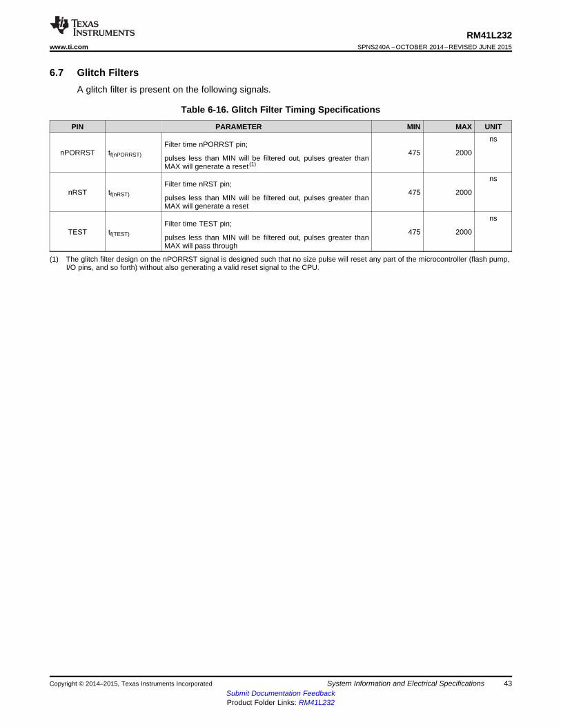
RM41L232www.ti.com SPNS240A –OCTOBER 2014–REVISED JUNE 2015
6.7 Glitch FiltersA glitch filter is present on the following signals.
Table 6-16. Glitch Filter Timing Specifications
PIN PARAMETER MIN MAX UNITns
Filter time nPORRST pin;nPORRST tf(nPORRST) 475 2000
pulses less than MIN will be filtered out, pulses greater thanMAX will generate a reset (1)
nsFilter time nRST pin;
nRST tf(nRST) 475 2000pulses less than MIN will be filtered out, pulses greater thanMAX will generate a reset
nsFilter time TEST pin;
TEST tf(TEST) 475 2000pulses less than MIN will be filtered out, pulses greater thanMAX will pass through
(1) The glitch filter design on the nPORRST signal is designed such that no size pulse will reset any part of the microcontroller (flash pump,I/O pins, and so forth) without also generating a valid reset signal to the CPU.
Copyright © 2014–2015, Texas Instruments Incorporated System Information and Electrical Specifications 43Submit Documentation FeedbackProduct Folder Links: RM41L232

Flash (128KB)
RAM (32KB)
0x00000000
0x0001FFFF
0x08000000
0x08007FFF
CRC0xFE000000
Peripherals - Frame 1
0xFF0000000xFFF7FFFF
SYSTEM Modules0xFFF80000
0xFFFFFFFF
0xF0000000
RAM - ECC0x08400000
0x08407FFF
RESERVED
RESERVED
Flash (128KB) (Mirrored Image)0x20000000
0x2001FFFF
RESERVED
RESERVED
0xF07FFFFF
RESERVED
Flash Module Bus2 Interface(Flash ECC, OTP and EEPROM accesses)
Peripherals - Frame 20xFC000000
0xFCFFFFFF
RESERVED
RM41L232SPNS240A –OCTOBER 2014–REVISED JUNE 2015 www.ti.com
6.8 Device Memory Map
6.8.1 Memory Map DiagramFigure 6-9 shows the device memory map.
Figure 6-9. RM41LS232 Memory Map
The Flash memory in all configurations is mirrored to support ECC logic testing. The base address of themirrored Flash image is 0x2000 0000.
44 System Information and Electrical Specifications Copyright © 2014–2015, Texas Instruments IncorporatedSubmit Documentation FeedbackProduct Folder Links: RM41L232
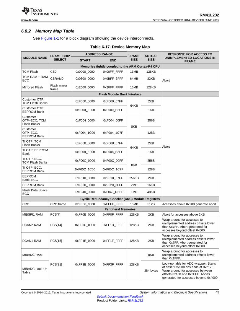
RM41L232www.ti.com SPNS240A –OCTOBER 2014–REVISED JUNE 2015
6.8.2 Memory Map TableSee Figure 1-1 for a block diagram showing the device interconnects.
Table 6-17. Device Memory Map
ADDRESS RANGE RESPONSE FOR ACCESS TOFRAME CHIP FRAME ACTUALMODULE NAME UNIMPLEMENTED LOCATIONS INSELECT SIZE SIZESTART END FRAMEMemories tightly coupled to the ARM Cortex-R4 CPU
TCM Flash CS0 0x0000_0000 0x00FF_FFFF 16MB 128KBTCM RAM + RAM CSRAM0 0x0800_0000 0x0BFF_3FFF 64MB 32KBECC Abort
Flash mirrorMirrored Flash 0x2000_0000 0x20FF_FFFF 16MB 128KBframeFlash Module Bus2 Interface
Customer OTP, 0xF000_0000 0xF000_07FF 2KBTCM Flash Banks64KB
Customer OTP, 0xF000_E000 0xF000_E3FF 1KBEEPROM BankCustomerOTP–ECC, TCM 0xF004_0000 0xF004_00FF 256BFlash Banks
8KBCustomerOTP–ECC, 0xF004_1C00 0xF004_1C7F 128BEEPROM BankTI OTP, TCM 0xF008_0000 0xF008_07FF 2KBFlash Banks Abort64KBTI OTP, EEPROM 0xF008_E000 0xF008_E3FF 1KBBankTI OTP–ECC, 0xF00C_0000 0xF00C_00FF 256BTCM Flash Banks
8KBTI OTP–ECC, 0xF00C_1C00 0xF00C_1C7F 128BEEPROM BankEEPROM 0xF010_0000 0xF010_07FF 256KB 2KBBank–ECCEEPROM Bank 0xF020_0000 0xF020_3FFF 2MB 16KBFlash Data Space 0xF040_0000 0xF040_DFFF 1MB 48KBECC
Cyclic Redundancy Checker (CRC) Module RegistersCRC CRC frame 0xFE00_0000 0xFEFF_FFFF 16MB 512B Accesses above 0x200 generate abort.
Peripheral MemoriesMIBSPI1 RAM PCS[7] 0xFF0E_0000 0xFF0F_FFFF 128KB 2KB Abort for accesses above 2KB
Wrap around for accesses tounimplemented address offsets lowerDCAN2 RAM PCS[14] 0xFF1C_0000 0xFF1D_FFFF 128KB 2KB than 0x7FF. Abort generated foraccesses beyond offset 0x800.Wrap around for accesses tounimplemented address offsets lowerDCAN1 RAM PCS[15] 0xFF1E_0000 0xFF1F_FFFF 128KB 2KB than 0x7FF. Abort generated foraccesses beyond offset 0x800.Wrap around for accesses to
MIBADC RAM 8KB unimplemented address offsets lowerthan 0x1FFF.Look-up table for ADC wrapper. StartsPCS[31] 0xFF3E_0000 0xFF3F_FFFF 128KBat offset 0x2000 ans ends at 0x217F.MIBADC Look-Up 384 bytes Wrap around for accesses betweenTable offsets 0x180 and 0x3FFF. Abortsgenerated for accesses beyond 0x4000
Copyright © 2014–2015, Texas Instruments Incorporated System Information and Electrical Specifications 45Submit Documentation FeedbackProduct Folder Links: RM41L232

RM41L232SPNS240A –OCTOBER 2014–REVISED JUNE 2015 www.ti.com
Table 6-17. Device Memory Map (continued)ADDRESS RANGE RESPONSE FOR ACCESS TOFRAME CHIP FRAME ACTUALMODULE NAME UNIMPLEMENTED LOCATIONS INSELECT SIZE SIZESTART END FRAME
Wrap around for accesses tounimplemented address offsets lowerN2HET RAM PCS[35] 0xFF46_0000 0xFF47_FFFF 128KB 16KB than 0x3FFF. Abort generated foraccesses beyond 0x3FFF.
HTU RAM PCS[39] 0xFF4E_0000 0xFF4F_FFFF 128KB 1KB AbortDebug Components
CoreSight Debug Reads return zeros, writes have noCSCS0 0xFFA0_0000 0xFFA0_0FFF 4KB 4KBROM effectReads return zeros, writes have noCortex-R4 Debug CSCS1 0xFFA0_1000 0xFFA0_1FFF 4KB 4KB effect
Peripheral Control RegistersReads return zeros, writes have noHTU PS[22] 0xFFF7_A400 0xFFF7_A4FF 256B 256B effectReads return zeros, writes have noN2HET PS[17] 0xFFF7_B800 0xFFF7_B8FF 256B 256B effectReads return zeros, writes have noGIO PS[16] 0xFFF7_BC00 0xFFF7_BCFF 256B 256B effectReads return zeros, writes have noMIBADC PS[15] 0xFFF7_C000 0xFFF7_C1FF 512B 512B effectReads return zeros, writes have noDCAN1 PS[8] 0xFFF7_DC00 0xFFF7_DDFF 512B 512B effectReads return zeros, writes have noDCAN2 PS[8] 0xFFF7_DE00 0xFFF7_DFFF 512B 512B effectReads return zeros, writes have noLIN PS[6] 0xFFF7_E400 0xFFF7_E4FF 256B 256B effectReads return zeros, writes have noMibSPI1 PS[2] 0xFFF7_F400 0xFFF7_F5FF 512B 512B effectReads return zeros, writes have noSPI2 PS[2] 0xFFF7_F600 0xFFF7_F7FF 512B 512B effectReads return zeros, writes have noSPI3 PS[1] 0xFFF7_F800 0xFFF7_F9FF 512B 512B effectReads return zeros, writes have noEQEP PS[25] 0xFFF7_9900 0xFFF7_99FF 256B 256B effectReads return zeros, writes have noEQEP (Mirrored) PS2[25] 0xFCF7_9900 0xFCF7_99FF 256B 256B effect
System Modules Control Registers and MemoriesWrap around for accesses tounimplemented address offsets lowerVIM RAM PPCS2 0xFFF8_2000 0xFFF8_2FFF 4KB 1KB than 0x3FF. Accesses beyond 0x3FFwill be ignored.
Flash Wrapper PPCS7 0xFFF8_7000 0xFFF8_7FFF 4KB 4KB AborteFuse Farm PPCS12 0xFFF8_C000 0xFFF8_CFFF 4KB 4KB AbortController
Reads return zeros, writes have noPCR registers PPS0 0xFFFF_E000 0xFFFF_E0FF 256B 256B effectSystem Module - Reads return zeros, writes have noFrame 2 (see PPS0 0xFFFF_E100 0xFFFF_E1FF 256B 256B effectdevice TRM)
Reads return zeros, writes have noPBIST PPS1 0xFFFF_E400 0xFFFF_E5FF 512B 512B effectReads return zeros, writes have noSTC PPS1 0xFFFF_E600 0xFFFF_E6FF 256B 256B effect
IOMM Generates address error interrupt ifMultiplexing PPS2 0xFFFF_EA00 0xFFFF_EBFF 512B 512B enabled.control module
46 System Information and Electrical Specifications Copyright © 2014–2015, Texas Instruments IncorporatedSubmit Documentation FeedbackProduct Folder Links: RM41L232
RM41L232www.ti.com SPNS240A –OCTOBER 2014–REVISED JUNE 2015
Table 6-17. Device Memory Map (continued)ADDRESS RANGE RESPONSE FOR ACCESS TOFRAME CHIP FRAME ACTUALMODULE NAME UNIMPLEMENTED LOCATIONS INSELECT SIZE SIZESTART END FRAME
Reads return zeros, writes have noDCC PPS3 0xFFFF_EC00 0xFFFF_ECFF 256B 256B effectReads return zeros, writes have noESM PPS5 0xFFFF_F500 0xFFFF_F5FF 256B 256B effectReads return zeros, writes have noCCMR4 PPS5 0xFFFF_F600 0xFFFF_F6FF 256B 256B effectReads return zeros, writes have noRAM ECC even PPS6 0xFFFF_F800 0xFFFF_F8FF 256B 256B effectReads return zeros, writes have noRAM ECC odd PPS6 0xFFFF_F900 0xFFFF_F9FF 256B 256B effectReads return zeros, writes have noRTI + DWWD PPS7 0xFFFF_FC00 0xFFFF_FCFF 256B 256B effectReads return zeros, writes have noVIM Parity PPS7 0xFFFF_FD00 0xFFFF_FDFF 256B 256B effectReads return zeros, writes have noVIM PPS7 0xFFFF_FE00 0xFFFF_FEFF 256B 256B effect
System Module - Reads return zeros, writes have noFrame 1 (see PPS7 0xFFFF_FF00 0xFFFF_FFFF 256B 256B effectdevice TRM)
Copyright © 2014–2015, Texas Instruments Incorporated System Information and Electrical Specifications 47Submit Documentation FeedbackProduct Folder Links: RM41L232

RM41L232SPNS240A –OCTOBER 2014–REVISED JUNE 2015 www.ti.com
6.8.3 Master/Slave Access PrivilegesThe table below lists the access permissions for each bus master on the device. A bus master is a modulethat can initiate a read or a write transaction on the device.
Each slave module on the main interconnect is listed in the table. A "Yes" indicates that the module listedin the "MASTERS" column can access that slave module.
Table 6-18. Master / Slave Access Matrix
SLAVES ON MAIN SCRPeripheral Control
Registers, AllFlash Module Bus2 Non-CPU Accesses PeripheralMASTERS ACCESS MODE Interface: to Program Flash CRC Memories, And AllOTP, ECC, EEPROM and CPU Data RAM System ModuleBank Control RegistersAnd Memories
CPU READ User/Privilege Yes Yes Yes YesCPU WRITE User/Privilege No Yes Yes Yes
HTU Privilege No Yes Yes Yes
48 System Information and Electrical Specifications Copyright © 2014–2015, Texas Instruments IncorporatedSubmit Documentation FeedbackProduct Folder Links: RM41L232
RM41L232www.ti.com SPNS240A –OCTOBER 2014–REVISED JUNE 2015
6.9 Flash Memory
6.9.1 Flash Memory ConfigurationFlash Bank: A separate block of logic consisting of 1 to 16 sectors. Each flash bank normally has acustomer-OTP and a TI-OTP area. These flash sectors share input/output buffers, data paths, senseamplifiers, and control logic.
Flash Sector: A contiguous region of flash memory which must be erased simultaneously due to physicalconstruction constraints.
Flash Pump: A charge pump which generates all the voltages required for reading, programming, orerasing the flash banks.
Flash Module: Interface circuitry required between the host CPU and the flash banks and pump module.
Note: The memory region from 0x0002_0000 to 0x0003_FFFF is not inherently protected against creatingnERROR pin toggles from speculative fetches or from run away code. An MPU region must be used tolimit accesses to only the first 128KB of ATCM space (0x0000_0000-0x0001_FFFF). Also, Flash APIversion 02.01.01 or later should be used to program or erase the flash of this device.
Table 6-19. Flash Memory Banks and Sectors
SECTORMEMORY ARRAYS (or BANKS) SEGMENT LOW ADDRESS HIGH ADDRESSNO.0 8KB 0x0000_0000 0x0000_1FFF1 8KB 0x0000_2000 0x0000_3FFF2 8KB 0x0000_4000 0x0000_5FFF3 8KB 0x0000_6000 0x0000_7FFF4 8KB 0x0000_8000 0x0000_9FFF5 8KB 0x0000_A000 0x0000_BFFF
BANK0 (128KB) (1) 6 8KB 0x0000_C000 0x0000_DFFF7 8KB 0x0000_E000 0x0000_FFFF8 8KB 0x0001_0000 0x0001_1FFF9 8KB 0x0001_2000 0x0001_3FFF10 8KB 0x0001_4000 0x0001_5FFF11 8KB 0x0001_6000 0x0001_7FFF12 32KB 0x0001_8000 0x0001_FFFF0 4KB 0xF020_0000 0xF020_0FFF1 4KB 0xF020_1000 0xF020_1FFF
BANK7 (16KB) for EEPROM emulation (2) (3)2 4KB 0xF020_2000 0xF020_2FFF3 4KB 0xF020_3000 0xF020_3FFF
(1) This Flash bank is 144-bit wide with ECC support.(2) Flash bank7 is an FLEE bank and can be programmed while executing code from flash bank0. It is 72-bit wide with ECC support.(3) Code execution is not allowed from flash bank7.
Copyright © 2014–2015, Texas Instruments Incorporated System Information and Electrical Specifications 49Submit Documentation FeedbackProduct Folder Links: RM41L232

RM41L232SPNS240A –OCTOBER 2014–REVISED JUNE 2015 www.ti.com
6.9.2 Main Features of Flash Module• Support for multiple flash banks for program and/or data storage• Simultaneous read access on a bank while performing program or erase operation on any other bank• Integrated state machines to automate flash erase and program operations• Software interface for flash program and erase operations• Pipelined mode operation to improve instruction access interface bandwidth• Support for Single Error Correction Double Error Detection (SECDED) block inside Cortex-R4 CPU
– Error address is captured for host system debugging• Support for a rich set of diagnostic features
6.9.3 ECC Protection for Flash AccessesAll accesses to the program flash memory are protected by Single Error Correction Double Error Detection(SECDED) logic embedded inside the CPU. The flash module provides 8 bits of ECC code for 64 bits ofinstructions or data fetched from the flash memory. The CPU calculates the expected ECC code based onthe 64 bits received and compares it with the ECC code returned by the flash module. A single-bit error iscorrected and flagged by the CPU, while a multibit error is only flagged. The CPU signals an ECC errorthrough its Event bus. This signaling mechanism is not enabled by default and must be enabled by settingthe "X" bit of the Performance Monitor Control Register, c9.
MRC p15,#0,r1,c9,c12,#0 ;Enabling Event monitor statesORR r1, r1, #0x00000010MCR p15,#0,r1,c9,c12,#0 ;Set 4th bit (‘X’) of PMNC registerMRC p15,#0,r1,c9,c12,#0
The application must also explicitly enable the CPU's ECC checking for accesses on the CPU's ATCMand BTCM interfaces. These are connected to the program flash and data RAM respectively. ECCchecking for these interfaces can be done by setting the B1TCMPCEN, B0TCMPCEN and ATCMPCENbits of the System Control coprocessor's Auxiliary Control Register, c1.
MRC p15, #0, r1, c1, c0, #1ORR r1, r1, #0x0e000000 ;Enable ECC checking for ATCM and BTCMsDMBMCR p15, #0, r1, c1, c0, #1
6.9.4 Flash Access SpeedsFor information on flash memory access speeds and the relevant wait states required, see Section 5.6.
50 System Information and Electrical Specifications Copyright © 2014–2015, Texas Instruments IncorporatedSubmit Documentation FeedbackProduct Folder Links: RM41L232
RM41L232www.ti.com SPNS240A –OCTOBER 2014–REVISED JUNE 2015
6.10 Flash Program and Erase Timings for Program Flash
Table 6-20. Timing Specifications for Program Flash
PARAMETER MIN NOM MAX UNITtprog (144bit) Wide Word (144 bit) programming time 40 300 µs
-40°C to 105°C 4tprog (Total) 384KByte programming time (1) s0°C to 60°C, for first 1 225 cycles
-40°C to 105°C 0.30 4 sterase Sector/Bank erase time (2) 0°C to 60°C, for first 16 100 ms25 cycles
Write/erase cycles with 15 year Data Retentiontwec -40°C to 105°C 1000 cyclesrequirement
(1) This programming time includes overhead of state machine, but does not include data transfer time. The programming time assumesprogramming 144 bits at a time at the maximum specified operating frequency.
(2) During bank erase, the selected sectors are erased simultaneously. The time to erase the bank is specified as equal to the time to erasea sector.
6.11 Flash Program and Erase Timings for Data Flash
Table 6-21. Timing Specifications for Data Flash
PARAMETER MIN NOM MAX UNITtprog (72 bit) Wide Word (72 bit) programming time 47 300 µs
–40°C to 105°C 330tprog (Total) 16KB programming time (1) ms0°C to 60°C, for first 100 16525 cycles
–40°C to 105°C 0.200 8 sterase Sector/Bank erase time (2) 0°C to 60°C, for first 14 100 ms25 cycles
Write/erase cycles with 15 year Data Retentiontwec –40°C to 105°C 100000 cyclesrequirement
(1) This programming time includes overhead of state machine, but does not include data transfer time. The programming time assumesprogramming 72 bits at a time at the maximum specified operating frequency.
(2) During bank erase, the selected sectors are erased simultaneously. The time to erase the bank is specified as equal to the time to erasea sector.
Copyright © 2014–2015, Texas Instruments Incorporated System Information and Electrical Specifications 51Submit Documentation FeedbackProduct Folder Links: RM41L232
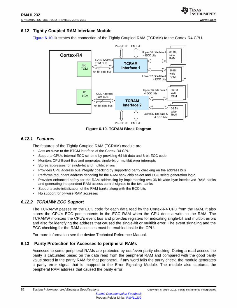
EVEN AddressTCM BUS
ODD AddressTCM BUS
64 Bit data bus
64 Bit data bus
Upper 32 bits data &4 ECC bits
Lower32 bits data &4 ECC bits
36 Bit
wideRAM
36 BitwideRAM
36 BitwideRAM
36 Bit
wideRAM
36 Bitwide
RAM
36 BitwideRAM
Upper 32 bits data &4 ECC bits
Lower32 bits data &
4 ECC bits
36 Bit
wide
RAM
36 Bit
wideRAM
36 BitwideRAM
36 Bit
wide
RAM
36 Bit
wideRAM
36 BitwideRAM
TCRAM
Interface 1
PMT I/FVBUSP I/F
Cortex-R4
B0TCM
B1
TCM
TCRAM
Interface 2
PMT I/FVBUSP I/F
RM41L232SPNS240A –OCTOBER 2014–REVISED JUNE 2015 www.ti.com
6.12 Tightly Coupled RAM Interface ModuleFigure 6-10 illustrates the connection of the Tightly Coupled RAM (TCRAM) to the Cortex-R4 CPU.
Figure 6-10. TCRAM Block Diagram
6.12.1 FeaturesThe features of the Tightly Coupled RAM (TCRAM) module are:• Acts as slave to the BTCM interface of the Cortex-R4 CPU• Supports CPU's internal ECC scheme by providing 64-bit data and 8-bit ECC code• Monitors CPU Event Bus and generates single-bit or multibit error interrupts• Stores addresses for single-bit and multibit errors• Provides CPU address bus integrity checking by supporting parity checking on the address bus• Performs redundant address decoding for the RAM bank chip select and ECC select generation logic• Provides enhanced safety for the RAM addressing by implementing two 36-bit wide byte-interleaved RAM banks
and generating independent RAM access control signals to the two banks• Supports auto-initialization of the RAM banks along with the ECC bits• No support for bit-wise RAM accesses
6.12.2 TCRAMW ECC SupportThe TCRAMW passes on the ECC code for each data read by the Cortex-R4 CPU from the RAM. It alsostores the CPU's ECC port contents in the ECC RAM when the CPU does a write to the RAM. TheTCRAMW monitors the CPU's event bus and provides registers for indicating single-bit and multibit errorsand also for identifying the address that caused the single-bit or multibit error. The event signaling and theECC checking for the RAM accesses must be enabled inside the CPU.
For more information see the device Technical Reference Manual.
6.13 Parity Protection for Accesses to peripheral RAMsAccesses to some peripheral RAMs are protected by odd/even parity checking. During a read access theparity is calculated based on the data read from the peripheral RAM and compared with the good parityvalue stored in the parity RAM for that peripheral. If any word fails the parity check, the module generatesa parity error signal that is mapped to the Error Signaling Module. The module also captures theperipheral RAM address that caused the parity error.
52 System Information and Electrical Specifications Copyright © 2014–2015, Texas Instruments IncorporatedSubmit Documentation FeedbackProduct Folder Links: RM41L232
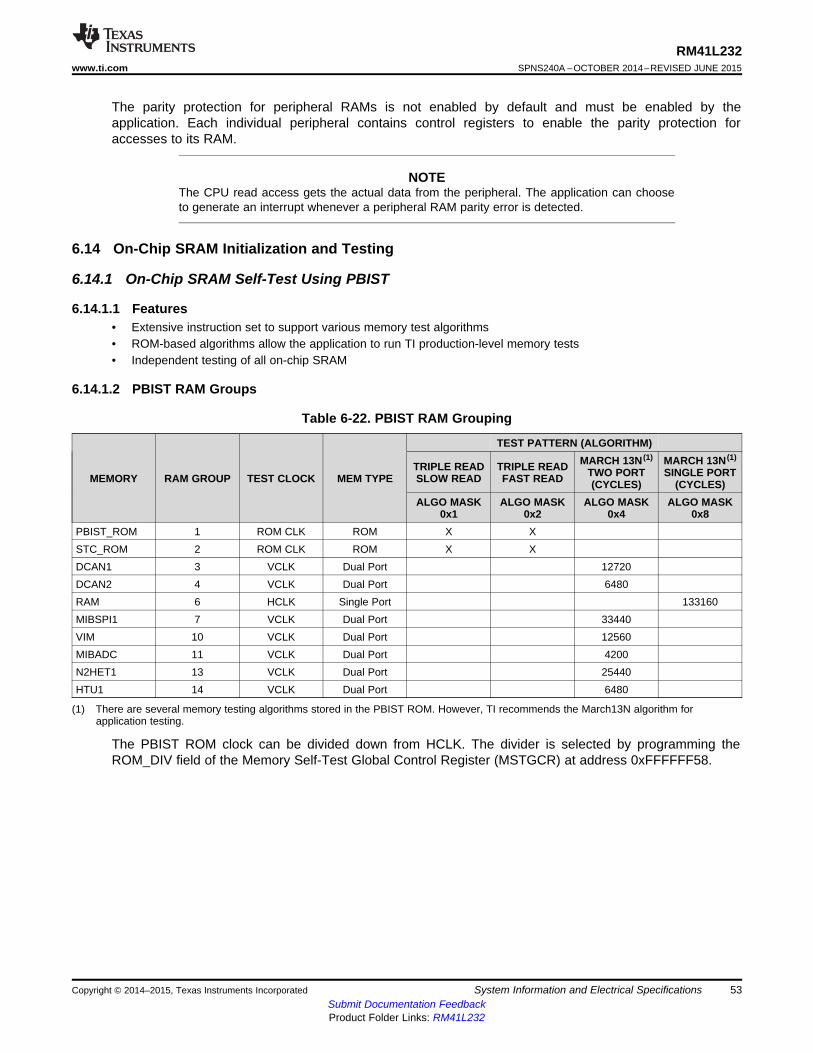
RM41L232www.ti.com SPNS240A –OCTOBER 2014–REVISED JUNE 2015
The parity protection for peripheral RAMs is not enabled by default and must be enabled by theapplication. Each individual peripheral contains control registers to enable the parity protection foraccesses to its RAM.
NOTEThe CPU read access gets the actual data from the peripheral. The application can chooseto generate an interrupt whenever a peripheral RAM parity error is detected.
6.14 On-Chip SRAM Initialization and Testing
6.14.1 On-Chip SRAM Self-Test Using PBIST
6.14.1.1 Features• Extensive instruction set to support various memory test algorithms• ROM-based algorithms allow the application to run TI production-level memory tests• Independent testing of all on-chip SRAM
6.14.1.2 PBIST RAM Groups
Table 6-22. PBIST RAM Grouping
TEST PATTERN (ALGORITHM)MARCH 13N (1) MARCH 13N (1)
TRIPLE READ TRIPLE READ TWO PORT SINGLE PORTMEMORY RAM GROUP TEST CLOCK MEM TYPE SLOW READ FAST READ (CYCLES) (CYCLES)ALGO MASK ALGO MASK ALGO MASK ALGO MASK
0x1 0x2 0x4 0x8PBIST_ROM 1 ROM CLK ROM X XSTC_ROM 2 ROM CLK ROM X XDCAN1 3 VCLK Dual Port 12720DCAN2 4 VCLK Dual Port 6480RAM 6 HCLK Single Port 133160MIBSPI1 7 VCLK Dual Port 33440VIM 10 VCLK Dual Port 12560MIBADC 11 VCLK Dual Port 4200N2HET1 13 VCLK Dual Port 25440HTU1 14 VCLK Dual Port 6480
(1) There are several memory testing algorithms stored in the PBIST ROM. However, TI recommends the March13N algorithm forapplication testing.
The PBIST ROM clock can be divided down from HCLK. The divider is selected by programming theROM_DIV field of the Memory Self-Test Global Control Register (MSTGCR) at address 0xFFFFFF58.
Copyright © 2014–2015, Texas Instruments Incorporated System Information and Electrical Specifications 53Submit Documentation FeedbackProduct Folder Links: RM41L232

RM41L232SPNS240A –OCTOBER 2014–REVISED JUNE 2015 www.ti.com
6.14.2 On-Chip SRAM Auto InitializationThis microcontroller allows some of the on-chip memories to be initialized through the Memory HardwareInitialization mechanism in the System module. This hardware mechanism allows an application toprogram the memory arrays with error detection capability to a known state based on their error detectionscheme (odd/even parity or ECC).
The MINITGCR register enables the memory initialization sequence, and the MSINENA register selectsthe memories that are to be initialized.
For more information on these registers refer to the device Technical Reference Manual.
The mapping of the different on-chip memories to the specific bits of the MSINENA registers is shown inTable 6-23.
Table 6-23. Memory Initialization
ADDRESS RANGE MSINENA REGISTERCONNECTING MODULE BIT NO. (1)BASE ADDRESS ENDING ADDRESSRAM 0x08000000 0x08007FFF 0MIBSPI1 RAM 0xFF0E0000 0xFF0FFFFF 7 (2)
DCAN2 RAM 0xFF1C0000 0xFF1DFFFF 6DCAN1 RAM 0xFF1E0000 0xFF1FFFFF 5MIBADC RAM 0xFF3E0000 0xFF3FFFFF 8N2HET RAM 0xFF460000 0xFF47FFFF 3HTU RAM 0xFF4E0000 0xFF4FFFFF 4VIM RAM 0xFFF82000 0xFFF82FFF 2
(1) Unassigned register bits are reserved.(2) The MibSPI1 module performs an initialization of the transmit and receive RAMs as soon as the module is brought out of reset using the
SPI Global Control Register 0 (SPIGCR0). This is independent of whether the application chooses to initialize the MibSPI1 RAMs usingthe system module auto-initialization method.
54 System Information and Electrical Specifications Copyright © 2014–2015, Texas Instruments IncorporatedSubmit Documentation FeedbackProduct Folder Links: RM41L232

RM41L232www.ti.com SPNS240A –OCTOBER 2014–REVISED JUNE 2015
6.15 Vectored Interrupt ManagerThe vectored interrupt manager (VIM) provides hardware assistance for prioritizing and controlling themany interrupt sources present on this device. Interrupts are caused by events outside of the normal flowof program execution. Normally, these events require a timely response from the central processing unit(CPU); therefore, when an interrupt occurs, the CPU switches execution from the normal program flow toan interrupt service routine (ISR).
6.15.1 VIM FeaturesThe VIM module has the following features:• Supports 96 interrupt channels.
– Provides programmable priority and enable for interrupt request lines.• Provides a direct hardware dispatch mechanism for fastest IRQ dispatch.• Provides two software dispatch mechanisms when the CPU VIC port is not used.
– Index interrupt– Register vectored interrupt
• Parity protected vector interrupt table against soft errors.
6.15.2 Interrupt Request Assignments
Table 6-24. Interrupt Request Assignments
DEFAULT VIMMODULES INTERRUPT SOURCES INTERRUPT
CHANNELESM ESM High level interrupt (NMI) 0
Reserved Reserved 1RTI RTI compare interrupt 0 2RTI RTI compare interrupt 1 3RTI RTI compare interrupt 2 4RTI RTI compare interrupt 3 5RTI RTI overflow interrupt 0 6RTI RTI overflow interrupt 1 7
Reserved Reserved 8GIO GIO interrupt A 9
N2HET N2HET level 0 interrupt 10HTU HTU level 0 interrupt 11
MIBSPI1 MIBSPI1 level 0 interrupt 12LIN LIN level 0 interrupt 13
MIBADC MIBADC event group interrupt 14MIBADC MIBADC sw group 1 interrupt 15DCAN1 DCAN1 level 0 interrupt 16
SPI2 SPI2 level 0 interrupt 17Reserved Reserved 18Reserved Reserved 19
ESM ESM Low level interrupt 20SYSTEM Software interrupt (SSI) 21
CPU PMU interrupt 22GIO GIO interrupt B 23
N2HET N2HET level 1 interrupt 24HTU HTU level 1 interrupt 25
Copyright © 2014–2015, Texas Instruments Incorporated System Information and Electrical Specifications 55Submit Documentation FeedbackProduct Folder Links: RM41L232

RM41L232SPNS240A –OCTOBER 2014–REVISED JUNE 2015 www.ti.com
Table 6-24. Interrupt Request Assignments (continued)DEFAULT VIM
MODULES INTERRUPT SOURCES INTERRUPTCHANNEL
MIBSPI1 MIBSPI1 level 1 interrupt 26LIN LIN level 1 interrupt 27
MIBADC MIBADC sw group 2 interrupt 28DCAN1 DCAN1 level 1 interrupt 29
SPI2 SPI2 level 1 interrupt 30MIBADC MIBADC magnitude compare interrupt 31Reserved Reserved 32-34DCAN2 DCAN2 level 0 interrupt 35
Reserved Reserved 36SPI3 SPI3 level 0 interrupt 37SPI3 SPI3 level 1 interrupt 38
Reserved Reserved 39-41DCAN2 DCAN2 level 1 interrupt 42
Reserved Reserved 43-60FMC FSM_DONE interrupt 61
Reserved Reserved 62-79HWAG HWA_INT_REQ_H 80
Reserved Reserved 81DCC DCC done interrupt 82
Reserved Reserved 83eQEPINTn eQEP Interrupt 84
PBIST PBIST Done Interrupt 85Reserved Reserved 86-87
HWAG HWA_INT_REQ_L 88Reserved Reserved 89-95
NOTEAddress location 0x00000000 in the VIM RAM is reserved for the phantom interrupt ISRentry; therefore only request channels 0..94 can be used and are offset by 1 address in theVIM RAM.
56 System Information and Electrical Specifications Copyright © 2014–2015, Texas Instruments IncorporatedSubmit Documentation FeedbackProduct Folder Links: RM41L232

31 0
31 0
RTICLK
31 0
31 0
31 0
Externalcontrol
CAP event source 0
CAP event source 1
=Up counter
Captureup counter
Compareup counter
Free running counter
Capture
RTIFRCx
free running counterRTICAFRCx
OVLINTx
RTICPUCx
RTIUCx
RTICAUCx
To Compare
Unit
RM41L232www.ti.com SPNS240A –OCTOBER 2014–REVISED JUNE 2015
6.16 Real-Time Interrupt ModuleThe real-time interrupt (RTI) module provides timer functionality for operating systems and forbenchmarking code. The RTI module can incorporate several counters that define the timebases neededfor scheduling an operating system.
The timers also allow you to benchmark certain areas of code by reading the values of the counters at thebeginning and the end of the desired code range and calculating the difference between the values.
6.16.1 FeaturesThe RTI module has the following features:• Two independent 64 bit counter blocks• Four configurable compares for generating operating system ticks. Each event can be driven by either
counter block 0 or counter block 1.• Fast enabling/disabling of events• Two time-stamp (capture) functions for system or peripheral interrupts, one for each counter block
6.16.2 Block DiagramsFigure 6-11 shows a high-level block diagram for one of the two 64-bit counter blocks inside the RTImodule. Both the counter blocks are identical.
Figure 6-11. Counter Block Diagram
Copyright © 2014–2015, Texas Instruments Incorporated System Information and Electrical Specifications 57Submit Documentation FeedbackProduct Folder Links: RM41L232
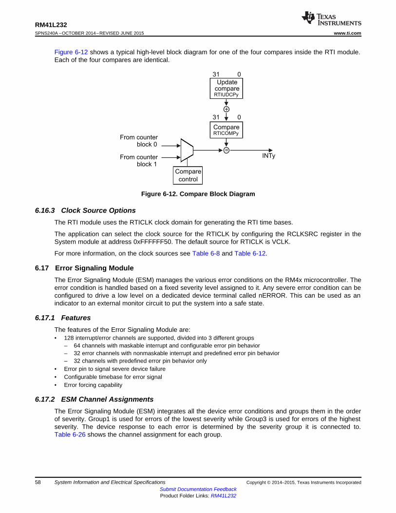
31 0
Compare
control
INTy
Compare
Updatecompare
From counterblock 0
From counterblock 1
RTIUDCPy
RTICOMPy
31 0
=
+
RM41L232SPNS240A –OCTOBER 2014–REVISED JUNE 2015 www.ti.com
Figure 6-12 shows a typical high-level block diagram for one of the four compares inside the RTI module.Each of the four compares are identical.
Figure 6-12. Compare Block Diagram
6.16.3 Clock Source OptionsThe RTI module uses the RTICLK clock domain for generating the RTI time bases.
The application can select the clock source for the RTICLK by configuring the RCLKSRC register in theSystem module at address 0xFFFFFF50. The default source for RTICLK is VCLK.
For more information, on the clock sources see Table 6-8 and Table 6-12.
6.17 Error Signaling ModuleThe Error Signaling Module (ESM) manages the various error conditions on the RM4x microcontroller. Theerror condition is handled based on a fixed severity level assigned to it. Any severe error condition can beconfigured to drive a low level on a dedicated device terminal called nERROR. This can be used as anindicator to an external monitor circuit to put the system into a safe state.
6.17.1 FeaturesThe features of the Error Signaling Module are:• 128 interrupt/error channels are supported, divided into 3 different groups
– 64 channels with maskable interrupt and configurable error pin behavior– 32 error channels with nonmaskable interrupt and predefined error pin behavior– 32 channels with predefined error pin behavior only
• Error pin to signal severe device failure• Configurable timebase for error signal• Error forcing capability
6.17.2 ESM Channel AssignmentsThe Error Signaling Module (ESM) integrates all the device error conditions and groups them in the orderof severity. Group1 is used for errors of the lowest severity while Group3 is used for errors of the highestseverity. The device response to each error is determined by the severity group it is connected to.Table 6-26 shows the channel assignment for each group.
58 System Information and Electrical Specifications Copyright © 2014–2015, Texas Instruments IncorporatedSubmit Documentation FeedbackProduct Folder Links: RM41L232
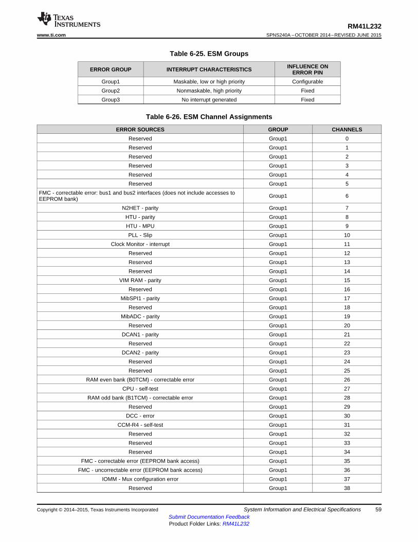
RM41L232www.ti.com SPNS240A –OCTOBER 2014–REVISED JUNE 2015
Table 6-25. ESM Groups
INFLUENCE ONERROR GROUP INTERRUPT CHARACTERISTICS ERROR PINGroup1 Maskable, low or high priority ConfigurableGroup2 Nonmaskable, high priority FixedGroup3 No interrupt generated Fixed
Table 6-26. ESM Channel Assignments
ERROR SOURCES GROUP CHANNELSReserved Group1 0Reserved Group1 1Reserved Group1 2Reserved Group1 3Reserved Group1 4Reserved Group1 5
FMC - correctable error: bus1 and bus2 interfaces (does not include accesses to Group1 6EEPROM bank)N2HET - parity Group1 7
HTU - parity Group1 8HTU - MPU Group1 9PLL - Slip Group1 10
Clock Monitor - interrupt Group1 11Reserved Group1 12Reserved Group1 13Reserved Group1 14
VIM RAM - parity Group1 15Reserved Group1 16
MibSPI1 - parity Group1 17Reserved Group1 18
MibADC - parity Group1 19Reserved Group1 20
DCAN1 - parity Group1 21Reserved Group1 22
DCAN2 - parity Group1 23Reserved Group1 24Reserved Group1 25
RAM even bank (B0TCM) - correctable error Group1 26CPU - self-test Group1 27
RAM odd bank (B1TCM) - correctable error Group1 28Reserved Group1 29
DCC - error Group1 30CCM-R4 - self-test Group1 31
Reserved Group1 32Reserved Group1 33Reserved Group1 34
FMC - correctable error (EEPROM bank access) Group1 35FMC - uncorrectable error (EEPROM bank access) Group1 36
IOMM - Mux configuration error Group1 37Reserved Group1 38
Copyright © 2014–2015, Texas Instruments Incorporated System Information and Electrical Specifications 59Submit Documentation FeedbackProduct Folder Links: RM41L232
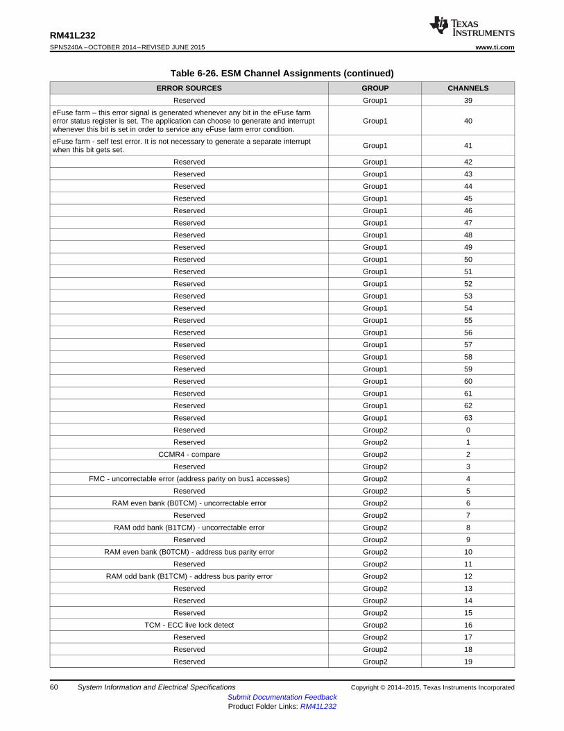
RM41L232SPNS240A –OCTOBER 2014–REVISED JUNE 2015 www.ti.com
Table 6-26. ESM Channel Assignments (continued)ERROR SOURCES GROUP CHANNELS
Reserved Group1 39eFuse farm – this error signal is generated whenever any bit in the eFuse farmerror status register is set. The application can choose to generate and interrupt Group1 40whenever this bit is set in order to service any eFuse farm error condition.eFuse farm - self test error. It is not necessary to generate a separate interrupt Group1 41when this bit gets set.
Reserved Group1 42Reserved Group1 43Reserved Group1 44Reserved Group1 45Reserved Group1 46Reserved Group1 47Reserved Group1 48Reserved Group1 49Reserved Group1 50Reserved Group1 51Reserved Group1 52Reserved Group1 53Reserved Group1 54Reserved Group1 55Reserved Group1 56Reserved Group1 57Reserved Group1 58Reserved Group1 59Reserved Group1 60Reserved Group1 61Reserved Group1 62Reserved Group1 63Reserved Group2 0Reserved Group2 1
CCMR4 - compare Group2 2Reserved Group2 3
FMC - uncorrectable error (address parity on bus1 accesses) Group2 4Reserved Group2 5
RAM even bank (B0TCM) - uncorrectable error Group2 6Reserved Group2 7
RAM odd bank (B1TCM) - uncorrectable error Group2 8Reserved Group2 9
RAM even bank (B0TCM) - address bus parity error Group2 10Reserved Group2 11
RAM odd bank (B1TCM) - address bus parity error Group2 12Reserved Group2 13Reserved Group2 14Reserved Group2 15
TCM - ECC live lock detect Group2 16Reserved Group2 17Reserved Group2 18Reserved Group2 19
60 System Information and Electrical Specifications Copyright © 2014–2015, Texas Instruments IncorporatedSubmit Documentation FeedbackProduct Folder Links: RM41L232

RM41L232www.ti.com SPNS240A –OCTOBER 2014–REVISED JUNE 2015
Table 6-26. ESM Channel Assignments (continued)ERROR SOURCES GROUP CHANNELS
Reserved Group2 20Reserved Group2 21Reserved Group2 22Reserved Group2 23
RTI_WWD_NMI Group2 24Reserved Group2 25Reserved Group2 26Reserved Group2 27Reserved Group2 28Reserved Group2 29Reserved Group2 30Reserved Group2 31Reserved Group3 0
eFuse Farm - autoload error Group3 1Reserved Group3 2
RAM even bank (B0TCM) - ECC uncorrectable error Group3 3Reserved Group3 4
RAM odd bank (B1TCM) - ECC uncorrectable error Group3 5Reserved Group3 6
FMC - uncorrectable error: bus1 and bus2 interfaces (does not include address Group3 7parity error and errors on accesses to EEPROM bank)Reserved Group3 8Reserved Group3 9Reserved Group3 10Reserved Group3 11Reserved Group3 12Reserved Group3 13Reserved Group3 14Reserved Group3 15Reserved Group3 16Reserved Group3 17Reserved Group3 18Reserved Group3 19Reserved Group3 20Reserved Group3 21Reserved Group3 22Reserved Group3 23Reserved Group3 24Reserved Group3 25Reserved Group3 26Reserved Group3 27Reserved Group3 28Reserved Group3 29Reserved Group3 30Reserved Group3 31
Copyright © 2014–2015, Texas Instruments Incorporated System Information and Electrical Specifications 61Submit Documentation FeedbackProduct Folder Links: RM41L232
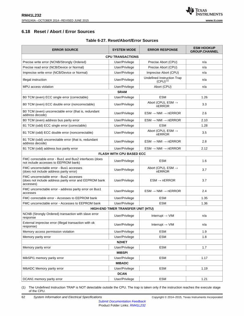
RM41L232SPNS240A –OCTOBER 2014–REVISED JUNE 2015 www.ti.com
6.18 Reset / Abort / Error Sources
Table 6-27. Reset/Abort/Error Sources
ESM HOOKUPERROR SOURCE SYSTEM MODE ERROR RESPONSE GROUP.CHANNELCPU TRANSACTIONS
Precise write error (NCNB/Strongly Ordered) User/Privilege Precise Abort (CPU) n/aPrecise read error (NCB/Device or Normal) User/Privilege Precise Abort (CPU) n/aImprecise write error (NCB/Device or Normal) User/Privilege Imprecise Abort (CPU) n/a
Undefined Instruction TrapIllegal instruction User/Privilege n/a(CPU) (1)
MPU access violation User/Privilege Abort (CPU) n/aSRAM
B0 TCM (even) ECC single error (correctable) User/Privilege ESM 1.26Abort (CPU), ESM →B0 TCM (even) ECC double error (noncorrectable) User/Privilege 3.3nERROR
B0 TCM (even) uncorrectable error (that is, redundant User/Privilege ESM → NMI → nERROR 2.6address decode)B0 TCM (even) address bus parity error User/Privilege ESM → NMI → nERROR 2.10B1 TCM (odd) ECC single error (correctable) User/Privilege ESM 1.28
Abort (CPU), ESM →B1 TCM (odd) ECC double error (noncorrectable) User/Privilege 3.5nERRORB1 TCM (odd) uncorrectable error (that is, redundant User/Privilege ESM → NMI → nERROR 2.8address decode)B1 TCM (odd) address bus parity error User/Privilege ESM → NMI → nERROR 2.12
FLASH WITH CPU BASED ECCFMC correctable error - Bus1 and Bus2 interfaces (does User/Privilege ESM 1.6not include accesses to EEPROM bank)FMC uncorrectable error - Bus1 accesses Abort (CPU), ESM →User/Privilege 3.7(does not include address parity error) nERRORFMC uncorrectable error - Bus2 accesses(does not include address parity error and EEPROM bank User/Privilege ESM → nERROR 3.7accesses)FMC uncorrectable error - address parity error on Bus1 User/Privilege ESM → NMI → nERROR 2.4accessesFMC correctable error - Accesses to EEPROM bank User/Privilege ESM 1.35FMC uncorrectable error - Accesses to EEPROM bank User/Privilege ESM 1.36
HIGH-END TIMER TRANSFER UNIT (HTU)NCNB (Strongly Ordered) transaction with slave error User/Privilege Interrupt → VIM n/aresponseExternal imprecise error (Illegal transaction with ok User/Privilege Interrupt → VIM n/aresponse)Memory access permission violation User/Privilege ESM 1.9Memory parity error User/Privilege ESM 1.8
N2HETMemory parity error User/Privilege ESM 1.7
MIBSPIMibSPI1 memory parity error User/Privilege ESM 1.17
MIBADCMibADC Memory parity error User/Privilege ESM 1.19
DCANDCAN1 memory parity error User/Privilege ESM 1.21
(1) The Undefined Instruction TRAP is NOT detectable outside the CPU. The trap is taken only if the instruction reaches the execute stageof the CPU.
62 System Information and Electrical Specifications Copyright © 2014–2015, Texas Instruments IncorporatedSubmit Documentation FeedbackProduct Folder Links: RM41L232

RM41L232www.ti.com SPNS240A –OCTOBER 2014–REVISED JUNE 2015
Table 6-27. Reset/Abort/Error Sources (continued)ESM HOOKUPERROR SOURCE SYSTEM MODE ERROR RESPONSE GROUP.CHANNEL
DCAN2 memory parity error User/Privilege ESM 1.23PLL
PLL slip error User/Privilege ESM 1.10CLOCK MONITOR
Clock monitor interrupt User/Privilege ESM 1.11DCC
DCC error User/Privilege ESM 1.30CCM-R4
Self test failure User/Privilege ESM 1.31Compare failure User/Privilege ESM → NMI → nERROR 2.2
VIMMemory parity error User/Privilege ESM 1.15
VOLTAGE MONITORVMON out of voltage range n/a Reset n/a
CPU SELF-TEST (LBIST)CPU Self-test (LBIST) error User/Privilege ESM 1.27
PIN MULTIPLEXING CONTROLMux configuration error User/Privilege ESM 1.37
eFuse CONTROLLEReFuse Controller Autoload error User/Privilege ESM → nERROR 3.1eFuse Controller - Any bit set in the error status register User/Privilege ESM 1.40eFuse Controller self-test error User/Privilege ESM 1.41
WINDOWED WATCHDOGWWD Nonmaskable Interrupt exception n/a ESM => NMI => nERROR 2.24
ERRORS REFLECTED IN THE SYSESR REGISTERPower-Up Reset n/a Reset n/aOscillator fail / PLL slip (2) n/a Reset n/aWatchdog exception n/a Reset n/aCPU Reset (driven by the CPU STC) n/a Reset n/aSoftware Reset n/a Reset n/aExternal Reset n/a Reset n/a
(2) Oscillator fail/PLL slip can be configured in the system register (SYS.PLLCTL1) to generate a reset.
6.19 Digital Windowed WatchdogThis device includes a digital windowed watchdog (DWWD) module that protects against runaway codeexecution.
The DWWD module allows the application to configure the time window within which the DWWD moduleexpects the application to service the watchdog. A watchdog violation occurs if the application services thewatchdog outside of this window, or fails to service the watchdog at all. The application can choose togenerate a system reset or a nonmaskable interrupt to the CPU in case of a watchdog violation.
The watchdog is disabled by default and must be enabled by the application. Once enabled, the watchdogcan only be disabled upon a system reset.
Copyright © 2014–2015, Texas Instruments Incorporated System Information and Electrical Specifications 63Submit Documentation FeedbackProduct Folder Links: RM41L232

TRSTTMSTCK
TDITDO
RTCK
ICE
PIC
K_
C
Boundary ScanBSR/BSDL
Boundary Scan I/F
Secondary Tap 0
DAP
Debug APB
DebugROM1
APB slave
CortexR4
Test Tap 0
eFuse Farm
Secondary Tap 2AJSM
RM41L232SPNS240A –OCTOBER 2014–REVISED JUNE 2015 www.ti.com
6.20 Debug Subsystem
6.20.1 Block DiagramThe device contains an ICEPICK module to allow JTAG access to the scan chains (see Figure 6-13).
Figure 6-13. Debug Subsystem Block Diagram
6.20.2 Debug Components Memory Map
Table 6-28. Debug Components Memory MapFRAME ADDRESS RANGEFRAME CHIP FRAME ACTUAL RESPONSE FOR ACCESS TOMODULE NAME SELECT SIZE SIZE UNIMPLEMENTED LOCATIONS IN FRAMESTART END
CoreSight Debug CSCS0 0xFFA0_0000 0xFFA0_0FFF 4KB 4KB Reads return zeros, writes have no effectROM
Cortex-R4 Debug CSCS1 0xFFA0_1000 0xFFA0_1FFF 4KB 4KB Reads return zeros, writes have no effect
6.20.3 JTAG Identification CodeThe JTAG ID code for this device is the same as the device ICEPick Identification Code.
Table 6-29. JTAG Identification Code
SILICON REVISION IDENTIFICATION CODEInitial Silicon 0x0B97102FRevision A 0x1B97102FRevision B 0x2B97102F
64 System Information and Electrical Specifications Copyright © 2014–2015, Texas Instruments IncorporatedSubmit Documentation FeedbackProduct Folder Links: RM41L232
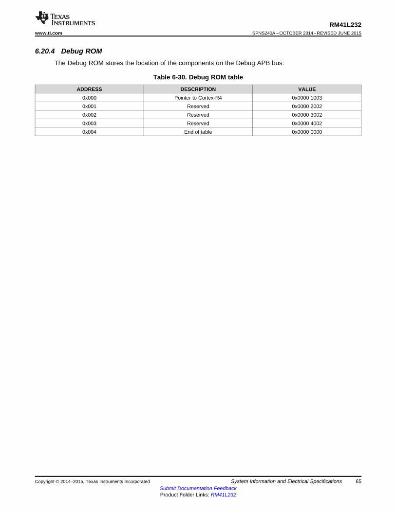
RM41L232www.ti.com SPNS240A –OCTOBER 2014–REVISED JUNE 2015
6.20.4 Debug ROMThe Debug ROM stores the location of the components on the Debug APB bus:
Table 6-30. Debug ROM table
ADDRESS DESCRIPTION VALUE0x000 Pointer to Cortex-R4 0x0000 10030x001 Reserved 0x0000 20020x002 Reserved 0x0000 30020x003 Reserved 0x0000 40020x004 End of table 0x0000 0000
Copyright © 2014–2015, Texas Instruments Incorporated System Information and Electrical Specifications 65Submit Documentation FeedbackProduct Folder Links: RM41L232

1 1
2
3
4
5
TMS
TDI
TDO
RTCK
TCK
RM41L232SPNS240A –OCTOBER 2014–REVISED JUNE 2015 www.ti.com
6.20.5 JTAG Scan Interface Timings
Table 6-31. JTAG Scan Interface Timing (1)
NO. PARAMETER MIN MAX UNITfTCK TCK frequency (at HCLKmax) 12 MHzfRTCK RTCK frequency (at TCKmax and HCLKmax) 10 MHz
1 td(TCK -RTCK) Delay time, TCK to RTCK 24 ns2 tsu(TDI/TMS - RTCKr) Setup time, TDI, TMS before RTCK rise (RTCKr) 26 ns3 th(RTCKr -TDI/TMS) Hold time, TDI, TMS after RTCKr 0 ns4 th(RTCKr -TDO) Hold time, TDO after RTCKf 0 ns5 td(TCKf -TDO) Delay time, TDO valid after RTCK fall (RTCKf) 12 ns
(1) Timings for TDO are specified for a maximum of 50 pF load on TDO
Figure 6-14. JTAG Timing
66 System Information and Electrical Specifications Copyright © 2014–2015, Texas Instruments IncorporatedSubmit Documentation FeedbackProduct Folder Links: RM41L232

H L H L H L L H
. . .. . .
128-bit comparator
H L L H H L L H
UNLOCK
Flash Module Output
OTP Contents
Unlock By Scan
Register
Internal Tie-Offs(example only)
(example)
L H H L LInternal Tie-Offs(example only)
L H H
RM41L232www.ti.com SPNS240A –OCTOBER 2014–REVISED JUNE 2015
6.20.6 Advanced JTAG Security ModuleThis device includes a an Advanced JTAG Security Module (AJSM). which provides maximum security tothe memory content of the device by allowing users to secure the device after programming.
Figure 6-15. AJSM Unlock
The device is unsecure by default by virtue of a 128-bit visible unlock code programmed in the OTPaddress 0xF0000000.The OTP contents are XOR-ed with the "Unlock By Scan" register contents. Theoutputs of these XOR gates are again combined with a set of secret internal tie-offs. The output of thiscombinational logic is compared against a secret hard-wired 128-bit value. A match results in theUNLOCK signal being asserted, so that the device is now unsecure.
A user can secure the device by changing at least one bit in the visible unlock code from 1 to 0. Changinga 0 to 1 is not possible because the visible unlock code is stored in the One Time Programmable (OTP)flash region. Also, changing all the 128 bits to zeros is not a valid condition and will permanently securethe device.
Once secured, a user can unsecure the device by scanning an appropriate value into the "Unlock ByScan" register of the AJSM module. The value to be scanned is such that the XOR of the OTP contentsand the Unlock-By-Scan register contents results in the original visible unlock code.
The Unlock-By-Scan register is reset only upon asserting power-on reset (nPORRST).
A secure device only permits JTAG accesses to the AJSM scan chain through the Secondary Tap # 2 ofthe ICEPick module. All other secondary taps, test taps and the boundary scan interface are notaccessible in this state.
Copyright © 2014–2015, Texas Instruments Incorporated System Information and Electrical Specifications 67Submit Documentation FeedbackProduct Folder Links: RM41L232

TRSTTMSTCK
TDITDO
RTCK
ICE
PIC
K
Boundary
BSDL
Boundary Scan InterfaceScan
Device Pins (conceptual)
TDI
TDO
RM41L232SPNS240A –OCTOBER 2014–REVISED JUNE 2015 www.ti.com
6.20.7 Boundary Scan ChainThe device supports BSDL-compliant boundary scan for testing pin-to-pin compatibility. The boundaryscan chain is connected to the Boundary Scan Interface of the ICEPICK module.
Figure 6-16. Boundary Scan Implementation (Conceptual Diagram)
Data is serially shifted into all boundary-scan buffers through TDI, and out through TDO.
68 System Information and Electrical Specifications Copyright © 2014–2015, Texas Instruments IncorporatedSubmit Documentation FeedbackProduct Folder Links: RM41L232
RM41L232www.ti.com SPNS240A –OCTOBER 2014–REVISED JUNE 2015
7 Peripheral Information and Electrical Specifications
7.1 Peripheral Legend
Table 7-1. Peripheral Legend
ABBREVIATION FULL NAMEMibADC Multibuffered Analog-to-Digital ConverterCCM-R4 CPU Compare Module – Cortex-R4
CRC Cyclic Redundancy CheckDCAN Controller Area NetworkDCC Dual Clock ComparatorESM Error Signaling ModuleGIO General-Purpose Input/OutputHTU High-End Timer Transfer UnitLIN Local Interconnect Network
MibSPI Multibuffered Serial Peripheral InterfaceN2HET Platform High-End Timer
RTI Real-Time Interrupt ModuleSCI Serial Communications InterfaceSPI Serial Peripheral InterfaceVIM Vectored Interrupt Manager
7.2 Multibuffered 12-Bit Analog-to-Digital ConverterThe multibuffered A-to-D converter (MibADC) has a separate power bus for its analog circuitry thatenhances the A-to-D performance by preventing digital switching noise on the logic circuitry which couldbe present on VSS and VCC from coupling into the A-to-D analog stage. All A-to-D specifications are givenwith respect to ADREFLO unless otherwise noted.
Table 7-2. MibADC Overview
DESCRIPTION VALUEResolution 12 bitsMonotonic Assured
Output conversion code 00h to FFFh [00 for VAI ≤ ADREFLO; FFF for VAI ≥ ADREFHI]
7.2.1 Features• 12-bit resolution• ADREFHI and ADREFLO pins (high and low reference voltages)• Total Sample/Hold/Convert time: 600 ns Typical Minimum at 30 MHz ADCLK• One memory region per conversion group is available (event, group 1, group 2)• Allocation of channels to conversion groups is completely programmable• Memory regions are serviced by interrupt• Programmable interrupt threshold counter is available for each group• Programmable magnitude threshold interrupt for each group for any one channel• Option to read either 8-, or 10-, or 12-bit values from memory regions• Single or continuous conversion modes• Embedded self-test• Embedded calibration logic• Enhanced power-down mode
– Optional feature to automatically power down ADC core when no conversion is in progress• External event pin (ADEVT) programmable as general-purpose I/O
Copyright © 2014–2015, Texas Instruments Incorporated Peripheral Information and Electrical Specifications 69Submit Documentation FeedbackProduct Folder Links: RM41L232

RM41L232SPNS240A –OCTOBER 2014–REVISED JUNE 2015 www.ti.com
7.2.2 Event Trigger OptionsThe ADC module supports three conversion groups: Event Group, Group1, and Group2. Each of thesethree groups can be configured to be hardware event-triggered. In that case, the application can selectfrom among eight event sources to be the trigger for the conversions of a group.
7.2.2.1 MIBADC Event Trigger Hookup
Table 7-3. MIBADC Event Trigger Hookup
SOURCE SELECT BITSEVENT NUMBER For G1, G2, or EVENT TRIGGER
(G1SRC[2:0], G2SRC[2:0], or EVSRC[2:0])1 000 ADEVT2 001 N2HET[8]3 010 N2HET[10]4 011 RTI compare 0 interrupt5 100 N2HET[12]6 101 N2HET[14]7 110 N2HET[17]8 111 N2HET[19]
NOTEFor ADEVT, N2HET trigger sources, the connection to the MibADC module trigger input ismade from the output side of the input buffer. This way, a trigger condition can be generatedeither by configuring the function as output onto the pad, or by driving the function from anexternal trigger source as input. If the mux controller module is used to select differentfunctionality instead of ADEVT or N2HET[x], care must be taken to disable these signalsfrom triggering conversions; there is no multiplexing on input connections.
NOTEFor the RTI compare 0 interrupt source, the connection is made directly from the output ofthe RTI module. That is, the interrupt condition can be used as a trigger source even if theactual interrupt is not signaled to the CPU.
70 Peripheral Information and Electrical Specifications Copyright © 2014–2015, Texas Instruments IncorporatedSubmit Documentation FeedbackProduct Folder Links: RM41L232

VS1
On-StateLeakage
Off-StateLeakages
VS2
VS24
23*IAIL
IAIL
IAIL
Rext
Rext
Rext
Pin SmuxRmux
PinSmux Rmux
PinSmux Rmux Ssamp Rsamp
Csamp
Cext IAIL
IAIL IAIL
IAIL
Cmux
Cext
Cext
RM41L232www.ti.com SPNS240A –OCTOBER 2014–REVISED JUNE 2015
7.2.3 ADC Electrical and Timing Specifications
Table 7-4. MibADC Recommended Operating Conditions
PARAMETER MIN MAX UNITADREFHI A-to-D high-voltage reference source ADREFLO VCCAD VADREFLO A-to-D low-voltage reference source VSSAD ADREFHI VVAI Analog input voltage ADREFLO ADREFHI V
Analog input clamp currentIAIC –2 2 mA(VAI < VSSAD – 0.3 or VAI > VCCAD + 0.3)
Table 7-5. MibADC Electrical Characteristics Over Full Ranges of Recommended Operating Conditions (1)
PARAMETER DESCRIPTION/CONDITIONS MIN TYP MAX UNIT
Analog input mux on-Rmux See Figure 7-1 95 250 Ωresistance
ADC sample switch on-Rsamp See Figure 7-1 60 250 Ωresistance
Cmux Input mux capacitance See Figure 7-1 7 16 pF
Csamp ADC sample capacitance See Figure 7-1 8 13 pF
VSSAD < VIN < VSSAD + 100 mV –300 –1 200
Analog off-state input VSSAD + 100 mV < VIN < VCCAD -IAIL VCCAD = 3.6 V MAX –200 –0.3 200 nAleakage current 200 mV
VCCAD - 200 mV < VIN < VCCAD –200 1 500
VSSAD < VIN < VSSAD + 100 mV –8 2
VSSAD + 100 mV < VIN < VCCAD -IAOSB Analog on-state input bias VCCAD = 3.6 V MAX –4 2 µA200 mV
VCCAD - 200 mV < VIN < VCCAD –4 12
IADREFHI ADREFHI input current ADREFHI = VCCAD, ADREFLO = VSSAD 3 mA
Normal operating mode (2) mAICCAD Static supply current
ADC core in power-down mode 5 µA
(1) 1 LSB = (ADREFHI – ADREFLO)/ 2n where n = 10 in 10-bit mode and 12 in 12-bit mode(2) See Section 5.7.
Figure 7-1. MibADC Input Equivalent Circuit
Copyright © 2014–2015, Texas Instruments Incorporated Peripheral Information and Electrical Specifications 71Submit Documentation FeedbackProduct Folder Links: RM41L232

RM41L232SPNS240A –OCTOBER 2014–REVISED JUNE 2015 www.ti.com
Table 7-6. MibADC Timing Specifications
PARAMETER MIN NOM MAX UNITtc(ADCLK)
(1) Cycle time, MibADC clock 33 nstd(SH)
(2) Delay time, sample and hold time 200 nsDelay time from ADC power on until first input can betd(PU-ADV) 1 µssampled
12-BIT MODEtd(C) Delay time, conversion time 400 nstd(SHC)
(3) Delay time, total sample/hold and conversion time 600 ns10-BIT MODE
td(C) Delay time, conversion time 330 nstd(SHC)
(3) Delay time, total sample/hold and conversion time 530 ns
(1) The MibADC clock is the ADCLK, generated by dividing down the VCLK by a prescale factor defined by the ADCLOCKCR register bits4:0.
(2) The sample and hold time for the ADC conversions is defined by the ADCLK frequency and the AD<GP>SAMP register for eachconversion group. The sample time must be determined by accounting for the external impedance connected to the input channel aswell as the internal impedance of the ADC.
(3) This is the minimum sample/hold and conversion time that can be achieved. These parameters are dependent on many factors forexample, the prescale settings.
72 Peripheral Information and Electrical Specifications Copyright © 2014–2015, Texas Instruments IncorporatedSubmit Documentation FeedbackProduct Folder Links: RM41L232
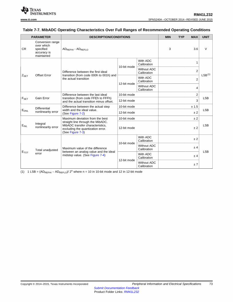
RM41L232www.ti.com SPNS240A –OCTOBER 2014–REVISED JUNE 2015
Table 7-7. MibADC Operating Characteristics Over Full Ranges of Recommended Operating Conditions
PARAMETER DESCRIPTION/CONDITIONS MIN TYP MAX UNITConversion rangeover which
CR specified ADREFHI - ADREFLO 3 3.6 Vaccuracy ismaintained
With ADC 1Calibration10-bit mode
Without ADC 2Difference between the first ideal CalibrationZSET Offset Error transition (from code 000h to 001h) and LSB (1)
With ADCthe actual transition 2Calibration12-bit mode
Without ADC 4CalibrationDifference between the last ideal 10-bit mode 2
FSET Gain Error transition (from code FFEh to FFFh) LSB12-bit mode 3and the actual transition minus offset.
Difference between the actual step 10-bit mode ± 1.5DifferentialEDNL width and the ideal value. LSBnonlinearity error 12-bit mode ± 2(See Figure 7-2)Maximum deviation from the best 10-bit mode ± 2straight line through the MibADC.IntegralEINL MibADC transfer characteristics, LSBnonlinearity error 12-bit mode ± 2excluding the quantization error.(See Figure 7-3)
With ADC ± 2Calibration10-bit mode
Without ADC ± 4Maximum value of the difference CalibrationTotal unadjustedETOT between an analog value and the ideal LSBerror With ADCmidstep value. (See Figure 7-4) ± 4Calibration12-bit mode
Without ADC ± 7Calibration
(1) 1 LSB = (ADREFHI – ADREFLO)/ 2n where n = 10 in 10-bit mode and 12 in 12-bit mode
Copyright © 2014–2015, Texas Instruments Incorporated Peripheral Information and Electrical Specifications 73Submit Documentation FeedbackProduct Folder Links: RM41L232
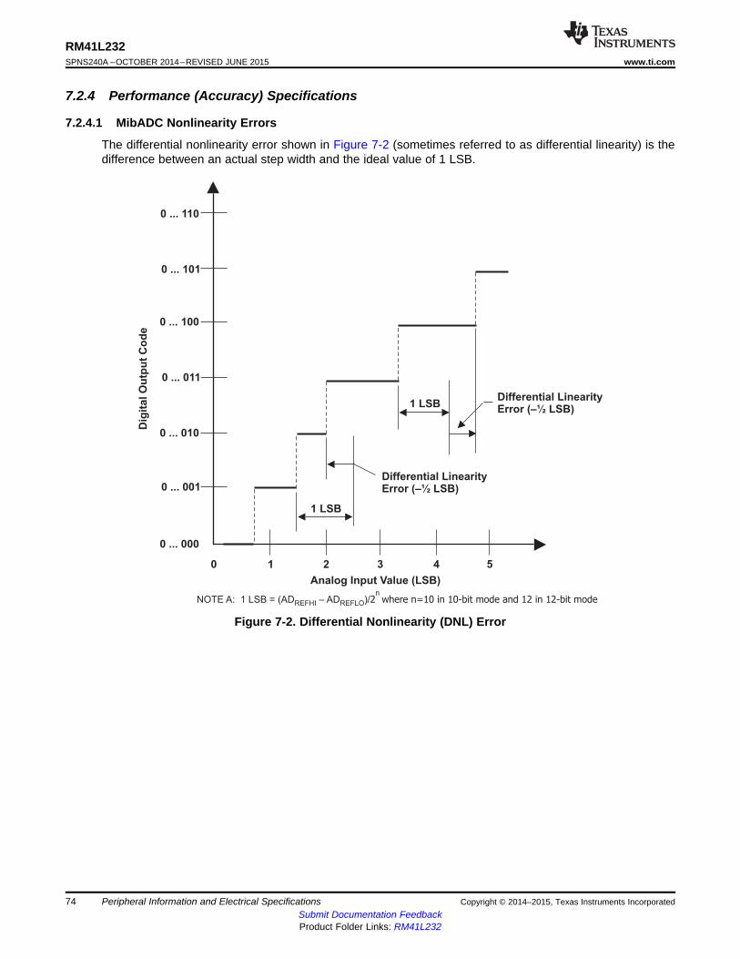
Differential LinearityError (–½ LSB)
1 LSB
1 LSB
Differential LinearityError (–½ LSB)
0 ... 110
0 ... 101
0 ... 100
0 ... 011
0 ... 010
0 ... 001
0 ... 000
0 1 2 3 4 5
Dig
ital O
utp
ut
Co
de
Analog Input Value (LSB)
NOTE A: 1 LSB = (AD – AD )/REFHI REFLO 2 where n=10 in 10-bit mode and 12 in 12-bit moden
RM41L232SPNS240A –OCTOBER 2014–REVISED JUNE 2015 www.ti.com
7.2.4 Performance (Accuracy) Specifications
7.2.4.1 MibADC Nonlinearity Errors
The differential nonlinearity error shown in Figure 7-2 (sometimes referred to as differential linearity) is thedifference between an actual step width and the ideal value of 1 LSB.
Figure 7-2. Differential Nonlinearity (DNL) Error
74 Peripheral Information and Electrical Specifications Copyright © 2014–2015, Texas Instruments IncorporatedSubmit Documentation FeedbackProduct Folder Links: RM41L232

0 ... 111
0 ... 101
0 ... 100
0 ... 011
0 ... 010
0 ... 001
0 ... 000
0 1 2 3 4 5
Dig
ital O
utp
ut
Co
de
Analog Input Value (LSB)
0 ... 110
6 7
At Transition011/100(–½ LSB)
At Transition001/010 (–1/4 LSB)
ActualTransition
IdealTransition
End-Point Lin. Error
NOTE A: 1 LSB = (AD – AD )/REFHI REFLO 2 where n=10 in 10-bit mode and 12 in 12-bit moden
RM41L232www.ti.com SPNS240A –OCTOBER 2014–REVISED JUNE 2015
The integral nonlinearity error shown in Figure 7-3 (sometimes referred to as linearity error) is thedeviation of the values on the actual transfer function from a straight line.
Figure 7-3. Integral Nonlinearity (INL) Error
Copyright © 2014–2015, Texas Instruments Incorporated Peripheral Information and Electrical Specifications 75Submit Documentation FeedbackProduct Folder Links: RM41L232
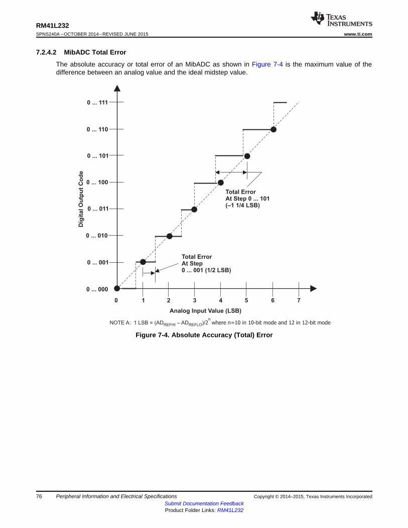
0 ... 111
0 ... 101
0 ... 100
0 ... 011
0 ... 010
0 ... 001
0 ... 000
0 1 2 3 4 5
Dig
ital O
utp
ut
Co
de
Analog Input Value (LSB)
0 ... 110
6 7
Total ErrorAt Step0 ... 001 (1/2 LSB)
Total ErrorAt Step 0 ... 101(–1 1/4 LSB)
NOTE A: 1 LSB = (AD – AD )/REFHI REFLO 2 where n=10 in 10-bit mode and 12 in 12-bit moden
RM41L232SPNS240A –OCTOBER 2014–REVISED JUNE 2015 www.ti.com
7.2.4.2 MibADC Total Error
The absolute accuracy or total error of an MibADC as shown in Figure 7-4 is the maximum value of thedifference between an analog value and the ideal midstep value.
Figure 7-4. Absolute Accuracy (Total) Error
76 Peripheral Information and Electrical Specifications Copyright © 2014–2015, Texas Instruments IncorporatedSubmit Documentation FeedbackProduct Folder Links: RM41L232
RM41L232www.ti.com SPNS240A –OCTOBER 2014–REVISED JUNE 2015
7.3 General-Purpose Input/OutputThe GPIO module on this device supports one port GIOA. The I/O pins are bidirectional and bit-programmable. GIOA supports external interrupt capability.
7.3.1 FeaturesThe GPIO module has the following features:• Each I/O pin can be configured as:
– Input– Output– Open Drain
• The interrupts have the following characteristics:– Programmable interrupt detection either on both edges or on a single edge (set in GIOINTDET)– Programmable edge-detection polarity, either rising or falling edge (set in GIOPOL register)– Individual interrupt flags (set in GIOFLG register)– Individual interrupt enables, set and cleared through GIOENASET and GIOENACLR registers
respectively– Programmable interrupt priority, set through GIOLVLSET and GIOLVLCLR registers
• Internal pullup/pulldown allows unused I/O pins to be left unconnected
For information on input and output timings see Section 5.11 and Section 5.12
Copyright © 2014–2015, Texas Instruments Incorporated Peripheral Information and Electrical Specifications 77Submit Documentation FeedbackProduct Folder Links: RM41L232
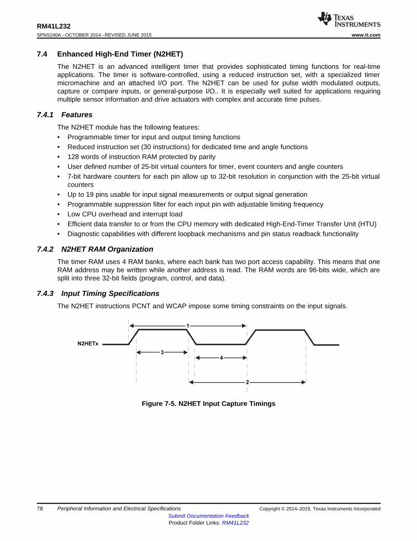
N2HETx
3
4
2
1
RM41L232SPNS240A –OCTOBER 2014–REVISED JUNE 2015 www.ti.com
7.4 Enhanced High-End Timer (N2HET)The N2HET is an advanced intelligent timer that provides sophisticated timing functions for real-timeapplications. The timer is software-controlled, using a reduced instruction set, with a specialized timermicromachine and an attached I/O port. The N2HET can be used for pulse width modulated outputs,capture or compare inputs, or general-purpose I/O.. It is especially well suited for applications requiringmultiple sensor information and drive actuators with complex and accurate time pulses.
7.4.1 FeaturesThe N2HET module has the following features:• Programmable timer for input and output timing functions• Reduced instruction set (30 instructions) for dedicated time and angle functions• 128 words of instruction RAM protected by parity• User defined number of 25-bit virtual counters for timer, event counters and angle counters• 7-bit hardware counters for each pin allow up to 32-bit resolution in conjunction with the 25-bit virtual
counters• Up to 19 pins usable for input signal measurements or output signal generation• Programmable suppression filter for each input pin with adjustable limiting frequency• Low CPU overhead and interrupt load• Efficient data transfer to or from the CPU memory with dedicated High-End-Timer Transfer Unit (HTU)• Diagnostic capabilities with different loopback mechanisms and pin status readback functionality
7.4.2 N2HET RAM OrganizationThe timer RAM uses 4 RAM banks, where each bank has two port access capability. This means that oneRAM address may be written while another address is read. The RAM words are 96-bits wide, which aresplit into three 32-bit fields (program, control, and data).
7.4.3 Input Timing SpecificationsThe N2HET instructions PCNT and WCAP impose some timing constraints on the input signals.
Figure 7-5. N2HET Input Capture Timings
78 Peripheral Information and Electrical Specifications Copyright © 2014–2015, Texas Instruments IncorporatedSubmit Documentation FeedbackProduct Folder Links: RM41L232

RM41L232www.ti.com SPNS240A –OCTOBER 2014–REVISED JUNE 2015
Table 7-8. Dynamic Characteristics for the N2HET Input Capture Functionality
PARAMETER MIN (1) (2) MAX (1) (2) UNITInput signal period, PCNT or WCAP for rising edge1 (hr)(lr) tc(VCLK2) + 2 225(hr)(lr)tc(VCLK2) - 2 nsto rising edgeInput signal period, PCNT or WCAP for falling edge2 (hr) (lr) tc(VCLK2) + 2 225 (hr)(lr) tc(VCLK2) - 2 nsto falling edgeInput signal high phase, PCNT or WCAP for rising3 2(hr) tc(VCLK2) + 2 225 (hr)(lr) tc(VCLK2) - 2 nsedge to falling edgeInput signal low phase, PCNT or WCAP for falling4 2(hr) tc(VCLK2) + 2 225 (hr)(lr) tc(VCLK2) - 2 nsedge to rising edge
(1) hr = High-resolution prescaler, configured using the HRPFC field of the Prescale Factor Register (HETPFR).(2) lr = Loop-resolution prescaler, configured using the LFPRC field of the Prescale Factor Register (HETPFR).
7.4.4 N2HET Checking
7.4.4.1 Output Monitoring using Dual Clock Comparator (DCC)
N2HET[31] is connected as a clock source for counter 1 in DCC1. This allows the application to measurethe frequency of the pulse-width modulated (PWM) signal on N2HET[31].
N2HET[31] can be configured to be an internal-only channel. That is, the connection to the DCC module ismade directly from the output of the N2HET module (from the input of the output buffer).
For more information on DCC, see Section 6.6.3.
7.4.5 Disabling N2HET OutputsSome applications require the N2HET outputs to be disabled under some fault condition. The N2HETmodule provides this capability through the "Pin Disable" input signal. This signal, when driven low,causes the N2HET outputs identified by a programmable register (HETPINDIS) to be tri-stated.
For more details on the "N2HET Pin Disable" feature, see the device-specific Technical Reference Manuallisted in Section 8.2.1.
GIOA[5] and EQEPERR are connected to the "Pin Disable" input for N2HET. In the case of GIOA[5]connection, this connection is made from the output of the input buffer. In the case of EQEPERR, theEQEPERR output signal is asserted in the event of a phase error. This signal is inverted and double-synchronized to VCLK2 for input into the N2HET PIN_nDISABLE port.
The PIN_nDISABLE port input source is selectable between the GIOA[5] and EQEPERR sources. This isachieved through the PINMMR9[1:0] bits.
Copyright © 2014–2015, Texas Instruments Incorporated Peripheral Information and Electrical Specifications 79Submit Documentation FeedbackProduct Folder Links: RM41L232
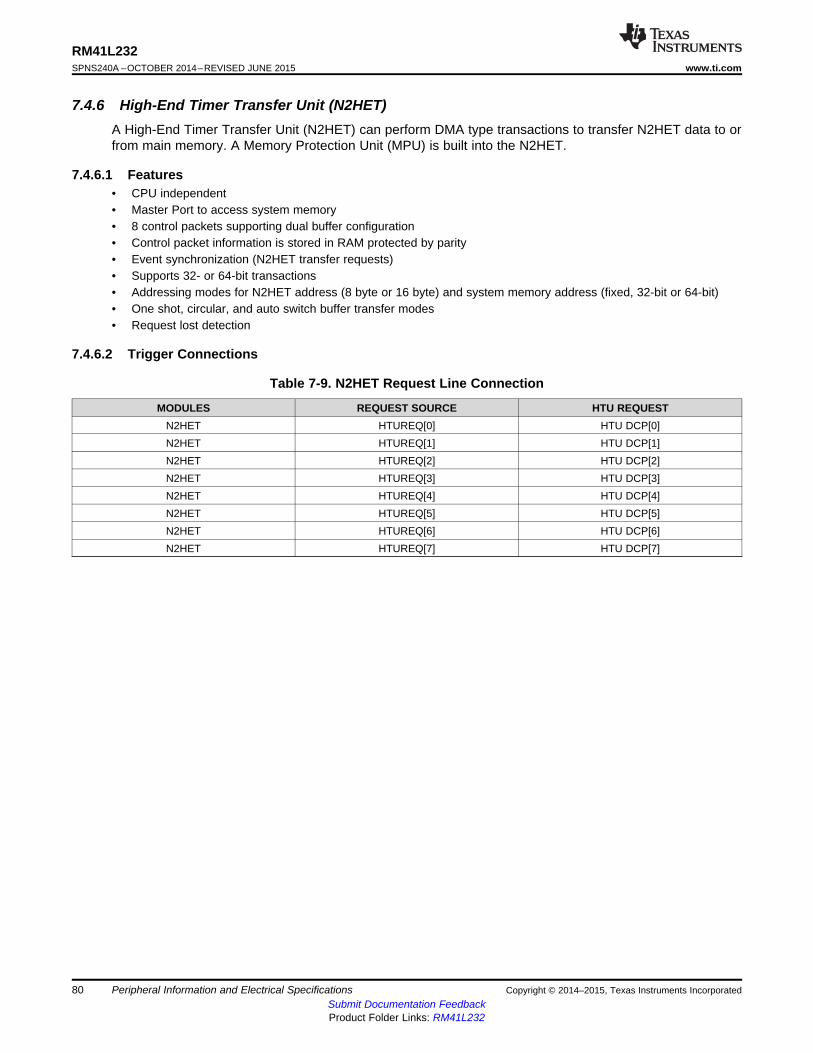
RM41L232SPNS240A –OCTOBER 2014–REVISED JUNE 2015 www.ti.com
7.4.6 High-End Timer Transfer Unit (N2HET)A High-End Timer Transfer Unit (N2HET) can perform DMA type transactions to transfer N2HET data to orfrom main memory. A Memory Protection Unit (MPU) is built into the N2HET.
7.4.6.1 Features• CPU independent• Master Port to access system memory• 8 control packets supporting dual buffer configuration• Control packet information is stored in RAM protected by parity• Event synchronization (N2HET transfer requests)• Supports 32- or 64-bit transactions• Addressing modes for N2HET address (8 byte or 16 byte) and system memory address (fixed, 32-bit or 64-bit)• One shot, circular, and auto switch buffer transfer modes• Request lost detection
7.4.6.2 Trigger Connections
Table 7-9. N2HET Request Line Connection
MODULES REQUEST SOURCE HTU REQUESTN2HET HTUREQ[0] HTU DCP[0]N2HET HTUREQ[1] HTU DCP[1]N2HET HTUREQ[2] HTU DCP[2]N2HET HTUREQ[3] HTU DCP[3]N2HET HTUREQ[4] HTU DCP[4]N2HET HTUREQ[5] HTU DCP[5]N2HET HTUREQ[6] HTU DCP[6]N2HET HTUREQ[7] HTU DCP[7]
80 Peripheral Information and Electrical Specifications Copyright © 2014–2015, Texas Instruments IncorporatedSubmit Documentation FeedbackProduct Folder Links: RM41L232
RM41L232www.ti.com SPNS240A –OCTOBER 2014–REVISED JUNE 2015
7.5 Controller Area Network (DCAN)The DCAN supports the CAN 2.0B protocol standard and uses a serial, multimaster communicationprotocol that efficiently supports distributed real-time control with robust communication rates of up to1 Mbps. The DCAN is ideal for applications operating in noisy and harsh environments (for example,automotive and industrial fields) that require reliable serial communication or multiplexed wiring.
7.5.1 FeaturesFeatures of the DCAN module include:• Supports CAN protocol version 2.0 part A, B• Bit rates up to 1 Mbps• The CAN kernel can be clocked by the oscillator for baud-rate generation.• 32 and 16 mailboxes on DCAN1 and DCAN2, respectively• Individual identifier mask for each message object• Programmable FIFO mode for message objects• Programmable loop-back modes for self-test operation• Automatic bus on after Bus-Off state by a programmable 32-bit timer• Message RAM protected by parity• Direct access to Message RAM during test mode• CAN RX / TX pins configurable as general-purpose I/O pins• Message RAM Auto Initialization
For more information on the DCAN, see the device-specific Technical Reference Manual listed inSection 8.2.1.
7.5.2 Electrical and Timing Specifications
Table 7-10. Dynamic Characteristics for the DCANx TX and RX pins
PARAMETER MIN MAX UNITtd(CANnTX) Delay time, transmit shift register to CANnTX pin (1) 15 nstd(CANnRX) Delay time, CANnRX pin to receive shift register 5 ns
(1) These values do not include rise/fall times of the output buffer.
Copyright © 2014–2015, Texas Instruments Incorporated Peripheral Information and Electrical Specifications 81Submit Documentation FeedbackProduct Folder Links: RM41L232
RM41L232SPNS240A –OCTOBER 2014–REVISED JUNE 2015 www.ti.com
7.6 Local Interconnect Network Interface (LIN)The SCI/LIN module can be programmed to work either as an SCI or as a LIN. The core of the module isan SCI. The SCI’s hardware features are augmented to achieve LIN compatibility.
The SCI module is a universal asynchronous receiver-transmitter that implements the standard nonreturnto zero format. The SCI can be used to communicate, for example, through an RS-232 port or over a K-line.
The LIN standard is based on the SCI (UART) serial data link format. The communication concept issingle-master/multiple-slave with a message identification for multicast transmission between any networknodes.
7.6.1 LIN FeaturesThe following are features of the LIN module:• Compatible to LIN 1.3, 2.0 and 2.1 protocols• Multibuffered receive and transmit units• Identification masks for message filtering• Automatic Master Header Generation
– Programmable Synch Break Field– Synch Field– Identifier Field
• Slave Automatic Synchronization– Synch break detection– Optional baudrate update– Synchronization Validation
• 231 programmable transmission rates with 7 fractional bits• Error detection• 2 Interrupt lines with priority encoding
82 Peripheral Information and Electrical Specifications Copyright © 2014–2015, Texas Instruments IncorporatedSubmit Documentation FeedbackProduct Folder Links: RM41L232

RM41L232www.ti.com SPNS240A –OCTOBER 2014–REVISED JUNE 2015
7.7 Multibuffered / Standard Serial Peripheral InterfaceThe MibSPI is a high-speed synchronous serial input/output port that allows a serial bit stream ofprogrammed length (2 to 16 bits) to be shifted in and out of the device at a programmed bit-transfer rate.Typical applications for the SPI include interfacing to external peripherals, such as I/Os, memories, displaydrivers, and ADCs.
7.7.1 FeaturesBoth Standard and MibSPI modules have the following features:• 16-bit shift register• Receive buffer register• 11-bit baud clock generator• SPICLK can be internally generated (master mode) or received from an external clock source (slave
mode)• Each word transferred can have a unique format• SPI I/Os not used in the communication can be used as digital input/output signals
Table 7-11. MibSPI/SPI Default Configurations
MibSPIx/SPIx I/OsMibSPI1 MIBSPI1SIMO[0], MIBSPI1SOMI[0], MIBSPI1CLK, MIBSPI1nCS[3:0], MIBSPI1nENASPI2 SPI2SIMO, SPI2SOMI, SPI2CLK, SPI2nCS[0]SPI3 SPI3SIMO, SPI3SOMI, SPI3CLK, SPI3nENA, SPI3nCS[0]
7.7.2 MibSPI Transmit and Receive RAM OrganizationThe Multibuffer RAM is comprised of 128 buffers. Each entry in the Multibuffer RAM consists of four parts:a 16-bit transmit field, a 16-bit receive field, a 16-bit control field, and a 16-bit status field. The MultibufferRAM can be partitioned into multiple transfer group with variable number of buffers each.
7.7.3 MibSPI Transmit Trigger EventsEach of the transfer groups can be configured individually. For each of the transfer groups a trigger eventand a trigger source can be chosen. A trigger event can be, for example, a rising edge or a permanent lowlevel at a selectable trigger source. Up to 15 trigger sources are available which can be used by eachtransfer group. These trigger options are listed in Table 7-12.
Copyright © 2014–2015, Texas Instruments Incorporated Peripheral Information and Electrical Specifications 83Submit Documentation FeedbackProduct Folder Links: RM41L232
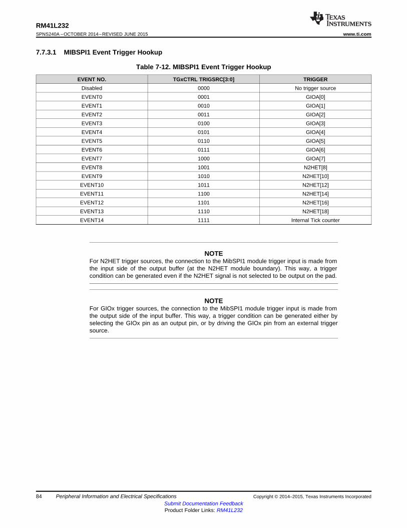
RM41L232SPNS240A –OCTOBER 2014–REVISED JUNE 2015 www.ti.com
7.7.3.1 MIBSPI1 Event Trigger Hookup
Table 7-12. MIBSPI1 Event Trigger Hookup
EVENT NO. TGxCTRL TRIGSRC[3:0] TRIGGERDisabled 0000 No trigger sourceEVENT0 0001 GIOA[0]EVENT1 0010 GIOA[1]EVENT2 0011 GIOA[2]EVENT3 0100 GIOA[3]EVENT4 0101 GIOA[4]EVENT5 0110 GIOA[5]EVENT6 0111 GIOA[6]EVENT7 1000 GIOA[7]EVENT8 1001 N2HET[8]EVENT9 1010 N2HET[10]EVENT10 1011 N2HET[12]EVENT11 1100 N2HET[14]EVENT12 1101 N2HET[16]EVENT13 1110 N2HET[18]EVENT14 1111 Internal Tick counter
NOTEFor N2HET trigger sources, the connection to the MibSPI1 module trigger input is made fromthe input side of the output buffer (at the N2HET module boundary). This way, a triggercondition can be generated even if the N2HET signal is not selected to be output on the pad.
NOTEFor GIOx trigger sources, the connection to the MibSPI1 module trigger input is made fromthe output side of the input buffer. This way, a trigger condition can be generated either byselecting the GIOx pin as an output pin, or by driving the GIOx pin from an external triggersource.
84 Peripheral Information and Electrical Specifications Copyright © 2014–2015, Texas Instruments IncorporatedSubmit Documentation FeedbackProduct Folder Links: RM41L232

RM41L232www.ti.com SPNS240A –OCTOBER 2014–REVISED JUNE 2015
7.7.4 MibSPI/SPI Master Mode I/O Timing Specifications
Table 7-13. SPI Master Mode External Timing Parameters (CLOCK PHASE = 0, SPICLK = output, SPISIMO= output, and SPISOMI = input) (1) (2) (3)
NO. PARAMETER MIN MAX UNIT
1 tc(SPC)M Cycle time, SPICLK (4) 40 256tc(VCLK) ns
Pulse duration, SPICLK high (clock polarity =tw(SPCH)M 0.5tc(SPC)M – tr(SPC)M – 3 0.5tc(SPC)M + 30)2 (5) ns
Pulse duration, SPICLK low (clock polarity =tw(SPCL)M 0.5tc(SPC)M – tf(SPC)M – 3 0.5tc(SPC)M + 31)
Pulse duration, SPICLK low (clock polarity =tw(SPCL)M 0.5tc(SPC)M – tf(SPC)M – 3 0.5tc(SPC)M + 30)3 (5) ns
Pulse duration, SPICLK high (clock polarity =tw(SPCH)M 0.5tc(SPC)M – tr(SPC)M – 3 0.5tc(SPC)M + 31)
Delay time, SPISIMO valid before SPICLKtd(SPCH-SIMO)M 0.5tc(SPC)M – 6low (clock polarity = 0)4 (5) ns
Delay time, SPISIMO valid before SPICLKtd(SPCL-SIMO)M 0.5tc(SPC)M – 6high (clock polarity = 1)
Valid time, SPISIMO data valid after SPICLKtv(SPCL-SIMO)M 0.5tc(SPC)M – tf(SPC) – 4low (clock polarity = 0)5 (5) ns
Valid time, SPISIMO data valid after SPICLKtv(SPCH-SIMO)M 0.5tc(SPC)M – tr(SPC) – 4high (clock polarity = 1)
Setup time, SPISOMI before SPICLK lowtsu(SOMI-SPCL)M tf(SPC) + 2.2(clock polarity = 0)6 (5) ns
Setup time, SPISOMI before SPICLK hightsu(SOMI-SPCH)M tr(SPC) + 2.2(clock polarity = 1)
Hold time, SPISOMI data valid after SPICLKth(SPCL-SOMI)M 10low (clock polarity = 0)7 (5) ns
Hold time, SPISOMI data valid after SPICLKth(SPCH-SOMI)M 10high (clock polarity = 1)
C2TDELAY*tc(VCLK) + 2*tc(VCLK) - (C2TDELAY+2) * tc(VCLK) - tf(SPICS) +CSHOLD = 0Setup time CS active until tf(SPICS) + tr(SPC) – 7 tr(SPC) + 5.5SPICLK high (clock ns
C2TDELAY*tc(VCLK) + 3*tc(VCLK) - (C2TDELAY+3) * tc(VCLK) - tf(SPICS) +polarity = 0) CSHOLD = 1 tf(SPICS) + tr(SPC) – 7 tr(SPC) + 5.58 (6) tC2TDELAY
C2TDELAY*tc(VCLK) + 2*tc(VCLK) - (C2TDELAY+2) * tc(VCLK) - tf(SPICS) +CSHOLD = 0Setup time CS active until tf(SPICS) + tf(SPC) – 7 tf(SPC) + 5.5SPICLK low (clock polarity ns
C2TDELAY*tc(VCLK) + 3*tc(VCLK) - (C2TDELAY+3) * tc(VCLK) - tf(SPICS) += 1) CSHOLD = 1 tf(SPICS) + tf(SPC) – 7 tf(SPC) + 5.5
Hold time SPICLK low until CS inactive 0.5*tc(SPC)M + T2CDELAY*tc(VCLK) + 0.5*tc(SPC)M + T2CDELAY*tc(VCLK) + ns(clock polarity = 0) tc(VCLK) - tf(SPC) + tr(SPICS) - 7 tc(VCLK) - tf(SPC) + tr(SPICS) + 119 (6) tT2CDELAY
Hold time SPICLK high until CS inactive 0.5*tc(SPC)M + T2CDELAY*tc(VCLK) + 0.5*tc(SPC)M + T2CDELAY*tc(VCLK) + ns(clock polarity = 1) tc(VCLK) - tr(SPC) + tr(SPICS) - 7 tc(VCLK) - tr(SPC) + tr(SPICS) + 11
(C2TDELAY+1) * tc(VCLK) - tf(SPICS) – ns10 tSPIENA SPIENAn Sample point (C2TDELAY+1)*tc(VCLK)29
11 tSPIENAW SPIENAn Sample point from write to buffer (C2TDELAY+2)*tc(VCLK) ns
(1) The MASTER bit (SPIGCR1.0) is set and the CLOCK PHASE bit (SPIFMTx.16) is cleared.(2) tc(VCLK) = interface clock cycle time = 1 / f(VCLK)(3) For rise and fall timings, see Table 5-6.(4) When the SPI is in Master mode, the following must be true:
For PS values from 1 to 255: tc(SPC)M ≥ (PS +1)tc(VCLK) ≥ 40 ns, where PS is the prescale value set in the SPIFMTx.[15:8] register bits.For PS values of 0: tc(SPC)M = 2tc(VCLK) ≥ 40 ns.The external load on the SPICLK pin must be less than 60 pF.
(5) The active edge of the SPICLK signal referenced is controlled by the CLOCK POLARITY bit (SPIFMTx.17).(6) C2TDELAY and T2CDELAY is programmed in the SPIDELAY register
Copyright © 2014–2015, Texas Instruments Incorporated Peripheral Information and Electrical Specifications 85Submit Documentation FeedbackProduct Folder Links: RM41L232
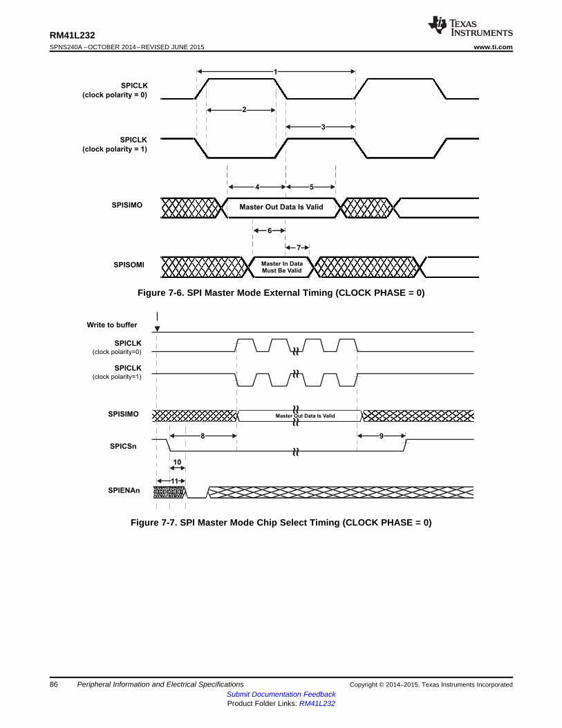
SPICLK
(clock polarity=0)
SPISIMO
SPICSn
Master Out Data Is Valid
9
SPICLK
(clock polarity=1)
SPIENAn
10
Write to buffer
11
8
SPISOMI
SPISIMO
SPICLK
(clock polarity = 1)
SPICLK
(clock polarity = 0)
Master In DataMust Be Valid
Master Out Data Is Valid
3
2
1
54
66
7
RM41L232SPNS240A –OCTOBER 2014–REVISED JUNE 2015 www.ti.com
Figure 7-6. SPI Master Mode External Timing (CLOCK PHASE = 0)
Figure 7-7. SPI Master Mode Chip Select Timing (CLOCK PHASE = 0)
86 Peripheral Information and Electrical Specifications Copyright © 2014–2015, Texas Instruments IncorporatedSubmit Documentation FeedbackProduct Folder Links: RM41L232
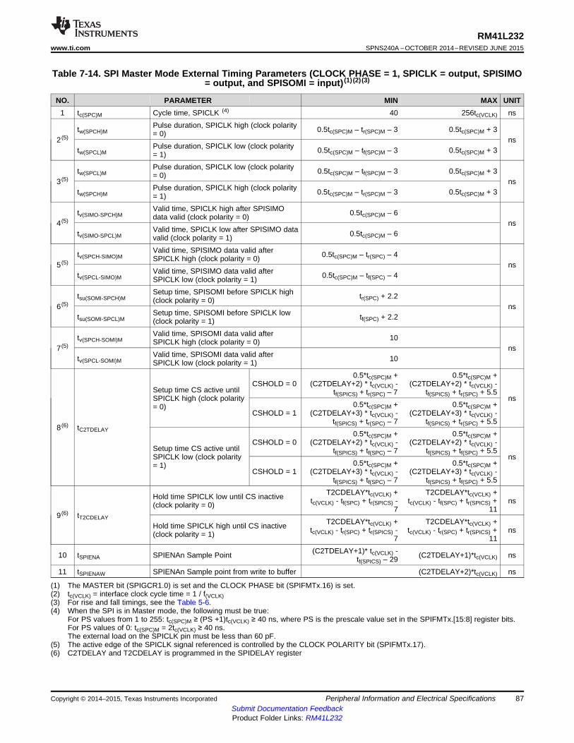
RM41L232www.ti.com SPNS240A –OCTOBER 2014–REVISED JUNE 2015
Table 7-14. SPI Master Mode External Timing Parameters (CLOCK PHASE = 1, SPICLK = output, SPISIMO= output, and SPISOMI = input) (1) (2) (3)
NO. PARAMETER MIN MAX UNIT1 tc(SPC)M Cycle time, SPICLK (4) 40 256tc(VCLK) ns
Pulse duration, SPICLK high (clock polaritytw(SPCH)M 0.5tc(SPC)M – tr(SPC)M – 3 0.5tc(SPC)M + 3= 0)2 (5) ns
Pulse duration, SPICLK low (clock polaritytw(SPCL)M 0.5tc(SPC)M – tf(SPC)M – 3 0.5tc(SPC)M + 3= 1)Pulse duration, SPICLK low (clock polaritytw(SPCL)M 0.5tc(SPC)M – tf(SPC)M – 3 0.5tc(SPC)M + 3= 0)
3 (5) nsPulse duration, SPICLK high (clock polaritytw(SPCH)M 0.5tc(SPC)M – tr(SPC)M – 3 0.5tc(SPC)M + 3= 1)Valid time, SPICLK high after SPISIMOtv(SIMO-SPCH)M 0.5tc(SPC)M – 6data valid (clock polarity = 0)
4 (5) nsValid time, SPICLK low after SPISIMO datatv(SIMO-SPCL)M 0.5tc(SPC)M – 6valid (clock polarity = 1)Valid time, SPISIMO data valid aftertv(SPCH-SIMO)M 0.5tc(SPC)M – tr(SPC) – 4SPICLK high (clock polarity = 0)
5 (5) nsValid time, SPISIMO data valid aftertv(SPCL-SIMO)M 0.5tc(SPC)M – tf(SPC) – 4SPICLK low (clock polarity = 1)Setup time, SPISOMI before SPICLK hightsu(SOMI-SPCH)M tr(SPC) + 2.2(clock polarity = 0)
6 (5) nsSetup time, SPISOMI before SPICLK lowtsu(SOMI-SPCL)M tf(SPC) + 2.2(clock polarity = 1)Valid time, SPISOMI data valid aftertv(SPCH-SOMI)M 10SPICLK high (clock polarity = 0)
7 (5) nsValid time, SPISOMI data valid aftertv(SPCL-SOMI)M 10SPICLK low (clock polarity = 1)
0.5*tc(SPC)M + 0.5*tc(SPC)M +CSHOLD = 0 (C2TDELAY+2) * tc(VCLK) - (C2TDELAY+2) * tc(VCLK) -
Setup time CS active until tf(SPICS) + tr(SPC) – 7 tf(SPICS) + tr(SPC) + 5.5SPICLK high (clock polarity ns
0.5*tc(SPC)M + 0.5*tc(SPC)M += 0)CSHOLD = 1 (C2TDELAY+3) * tc(VCLK) - (C2TDELAY+3) * tc(VCLK) -
tf(SPICS) + tr(SPC) – 7 tf(SPICS) + tr(SPC) + 5.58 (6) tC2TDELAY 0.5*tc(SPC)M + 0.5*tc(SPC)M +
CSHOLD = 0 (C2TDELAY+2) * tc(VCLK) - (C2TDELAY+2) * tc(VCLK) -Setup time CS active until tf(SPICS) + tf(SPC) – 7 tf(SPICS) + tf(SPC) + 5.5SPICLK low (clock polarity ns
0.5*tc(SPC)M + 0.5*tc(SPC)M += 1)CSHOLD = 1 (C2TDELAY+3) * tc(VCLK) - (C2TDELAY+3) * tc(VCLK) -
tf(SPICS) + tf(SPC) – 7 tf(SPICS) + tf(SPC) + 5.5T2CDELAY*tc(VCLK) + T2CDELAY*tc(VCLK) +Hold time SPICLK low until CS inactive tc(VCLK) - tf(SPC) + tr(SPICS) - tc(VCLK) - tf(SPC) + tr(SPICS) + ns(clock polarity = 0) 7 11
9 (6) tT2CDELAY T2CDELAY*tc(VCLK) + T2CDELAY*tc(VCLK) +Hold time SPICLK high until CS inactive tc(VCLK) - tr(SPC) + tr(SPICS) - tc(VCLK) - tr(SPC) + tr(SPICS) + ns(clock polarity = 1) 7 11(C2TDELAY+1)* tc(VCLK) -10 tSPIENA SPIENAn Sample Point (C2TDELAY+1)*tc(VCLK) nstf(SPICS) – 29
11 tSPIENAW SPIENAn Sample point from write to buffer (C2TDELAY+2)*tc(VCLK) ns
(1) The MASTER bit (SPIGCR1.0) is set and the CLOCK PHASE bit (SPIFMTx.16) is set.(2) tc(VCLK) = interface clock cycle time = 1 / f(VCLK)(3) For rise and fall timings, see the Table 5-6.(4) When the SPI is in Master mode, the following must be true:
For PS values from 1 to 255: tc(SPC)M ≥ (PS +1)tc(VCLK) ≥ 40 ns, where PS is the prescale value set in the SPIFMTx.[15:8] register bits.For PS values of 0: tc(SPC)M = 2tc(VCLK) ≥ 40 ns.The external load on the SPICLK pin must be less than 60 pF.
(5) The active edge of the SPICLK signal referenced is controlled by the CLOCK POLARITY bit (SPIFMTx.17).(6) C2TDELAY and T2CDELAY is programmed in the SPIDELAY register
Copyright © 2014–2015, Texas Instruments Incorporated Peripheral Information and Electrical Specifications 87Submit Documentation FeedbackProduct Folder Links: RM41L232
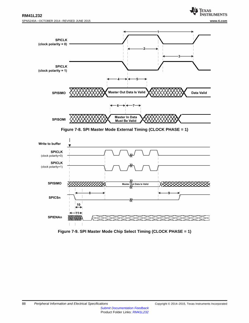
SPICLK
(clock polarity=0)
SPISIMO
SPICSn
Master Out Data Is Valid
9
SPICLK
(clock polarity=1)
SPIENAn
10
Write to buffer
11
8
SPISOMI
SPISIMO
SPICLK
(clock polarity = 1)
SPICLK
(clock polarity = 0)
Data Valid
Master In DataMust Be Valid
Master Out Data Is Valid
3
2
1
54
76
RM41L232SPNS240A –OCTOBER 2014–REVISED JUNE 2015 www.ti.com
Figure 7-8. SPI Master Mode External Timing (CLOCK PHASE = 1)
Figure 7-9. SPI Master Mode Chip Select Timing (CLOCK PHASE = 1)
88 Peripheral Information and Electrical Specifications Copyright © 2014–2015, Texas Instruments IncorporatedSubmit Documentation FeedbackProduct Folder Links: RM41L232

RM41L232www.ti.com SPNS240A –OCTOBER 2014–REVISED JUNE 2015
7.7.5 SPI Slave Mode I/O Timings
Table 7-15. SPI Slave Mode External Timing Parameters (CLOCK PHASE = 0, SPICLK = input, SPISIMO =input, and SPISOMI = output) (1) (2) (3) (4)
NO. PARAMETER MIN MAX UNIT1 tc(SPC)S Cycle time, SPICLK (5) 40 ns
tw(SPCH)S Pulse duration, SPICLK high (clock polarity = 0) 142 (6) ns
tw(SPCL)S Pulse duration, SPICLK low (clock polarity = 1) 14tw(SPCL)S Pulse duration, SPICLK low (clock polarity = 0) 14
3 (6) nstw(SPCH)S Pulse duration, SPICLK high (clock polarity = 1) 14td(SPCH-SOMI)S Delay time, SPISOMI valid after SPICLK high (clock polarity = 0) trf(SOMI) + 20
4 (6) nstd(SPCL-SOMI)S Delay time, SPISOMI valid after SPICLK low (clock polarity = 1) trf(SOMI) + 20
Hold time, SPISOMI data valid after SPICLK high (clock polarityth(SPCH-SOMI)S 2=0)5 (6) ns
Hold time, SPISOMI data valid after SPICLK low (clock polarityth(SPCL-SOMI)S 2=1)tsu(SIMO-SPCL)S Setup time, SPISIMO before SPICLK low (clock polarity = 0) 4
6 (6) nstsu(SIMO-SPCH)S Setup time, SPISIMO before SPICLK high (clock polarity = 1) 4
Hold time, SPISIMO data valid after SPICLK low (clock polarityth(SPCL-SIMO)S 2= 0)7 (6) ns
Hold time, SPISIMO data valid after S PICLK high (clock polarityth(SPCH-SIMO)S 2= 1)Delay time, SPIENAn high after last SPICLK low (clock polarity 2.5tc(VCLK)+tr(ENAtd(SPCL-SENAH)S 1.5tc(VCLK)= 0) n)+ 22
8 nsDelay time, SPIENAn high after last SPICLK high (clock polarity 2.5tc(VCLK)+td(SPCH-SENAH)S 1.5tc(VCLK)= 1) tr(ENAn) + 22Delay time, SPIENAn low after SPICSn low (if new data has tc(VCLK)+tf(ENAn)+9 td(SCSL-SENAL)S tf(ENAn) nsbeen written to the SPI buffer) 27
(1) The MASTER bit (SPIGCR1.0) is cleared and the CLOCK PHASE bit (SPIFMTx.16) is cleared.(2) If the SPI is in slave mode, the following must be true: tc(SPC)S ≥ (PS + 1) tc(VCLK), where PS = prescale value set in SPIFMTx.[15:8].(3) For rise and fall timings, see Table 5-6.(4) tc(VCLK) = interface clock cycle time = 1 /f(VCLK)(5) When the SPI is in Slave mode, the following must be true:
For PS values from 1 to 255: tc(SPC)S ≥ (PS +1)tc(VCLK) ≥ 40 ns, where PS is the prescale value set in the SPIFMTx.[15:8] register bits.For PS values of 0: tc(SPC)S = 2tc(VCLK) ≥ 40 ns.
(6) The active edge of the SPICLK signal referenced is controlled by the CLOCK POLARITY bit (SPIFMTx.17).
Copyright © 2014–2015, Texas Instruments Incorporated Peripheral Information and Electrical Specifications 89Submit Documentation FeedbackProduct Folder Links: RM41L232

SPICLK
(clock polarity=0)
SPICSn
8
SPICLK
(clock polarity=1)
SPIENAn
9
SPISOMI
SPICLK
(clock polarity = 1)
SPICLK
(clock polarity = 0)
3
2
1
54
7
SPISIMO DataMust Be Valid
SPISOMI Data Is Valid
666
SPISIMO
RM41L232SPNS240A –OCTOBER 2014–REVISED JUNE 2015 www.ti.com
Figure 7-10. SPI Slave Mode External Timing (CLOCK PHASE = 0)
Figure 7-11. SPI Slave Mode Enable Timing (CLOCK PHASE = 0)
90 Peripheral Information and Electrical Specifications Copyright © 2014–2015, Texas Instruments IncorporatedSubmit Documentation FeedbackProduct Folder Links: RM41L232

RM41L232www.ti.com SPNS240A –OCTOBER 2014–REVISED JUNE 2015
Table 7-16. SPI Slave Mode External Timing Parameters (CLOCK PHASE = 1, SPICLK = input, SPISIMO =input, and SPISOMI = output) (1) (2) (3) (4)
NO. PARAMETER MIN MAX UNIT
1 tc(SPC)S Cycle time, SPICLK (5) 40 ns
tw(SPCH)S Pulse duration, SPICLK high (clock polarity = 0) 142 (6) ns
tw(SPCL)S Pulse duration, SPICLK low (clock polarity = 1) 14
tw(SPCL)S Pulse duration, SPICLK low (clock polarity = 0) 143 (6) ns
tw(SPCH)S Pulse duration, SPICLK high (clock polarity = 1) 14
td(SOMI-SPCL)S Dealy time, SPISOMI data valid after SPICLK low (clock trf(SOMI) + 20polarity = 0)4 (6) ns
td(SOMI-SPCH)S Delay time, SPISOMI data valid after SPICLK high (clock trf(SOMI) + 20polarity = 1)
Hold time, SPISOMI data valid after SPICLK high (clockth(SPCL-SOMI)S 2polarity =0)5 (6) ns
Hold time, SPISOMI data valid after SPICLK low (clock polarityth(SPCH-SOMI)S 2=1)
tsu(SIMO-SPCH)S Setup time, SPISIMO before SPICLK high (clock polarity = 0) 46 (6) ns
tsu(SIMO-SPCL)S Setup time, SPISIMO before SPICLK low (clock polarity = 1) 4
High time, SPISIMO data valid after SPICLK high (clocktv(SPCH-SIMO)S 2polarity = 0)7 (6) ns
High time, SPISIMO data valid after SPICLK low (clock polaritytv(SPCL-SIMO)S 2= 1)
Delay time, SPIENAn high after last SPICLK high (clocktd(SPCH-SENAH)S 1.5tc(VCLK) 2.5tc(VCLK)+tr(ENAn) + 22polarity = 0)8 ns
Delay time, SPIENAn high after last SPICLK low (clock polaritytd(SPCL-SENAH)S 1.5tc(VCLK) 2.5tc(VCLK)+tr(ENAn) + 22= 1)
Delay time, SPIENAn low after SPICSn low (if new data has9 td(SCSL-SENAL)S tf(ENAn) tc(VCLK)+tf(ENAn)+ 27 nsbeen written to the SPI buffer)
Delay time, SOMI valid after SPICSn low (if new data has been10 td(SCSL-SOMI)S tc(VCLK) 2tc(VCLK)+trf(SOMI)+ 28 nswritten to the SPI buffer)
(1) The MASTER bit (SPIGCR1.0) is cleared and the CLOCK PHASE bit (SPIFMTx.16) is set.(2) If the SPI is in slave mode, the following must be true: tc(SPC)S ≤ (PS + 1) tc(VCLK), where PS = prescale value set in SPIFMTx.[15:8].(3) For rise and fall timings, see Table 5-6.(4) tc(VCLK) = interface clock cycle time = 1 /f(VCLK)(5) When the SPI is in Slave mode, the following must be true:
For PS values from 1 to 255: tc(SPC)S ≥ (PS +1)tc(VCLK) ≥ 40 ns, where PS is the prescale value set in the SPIFMTx.[15:8] register bits.For PS values of 0: tc(SPC)S = 2tc(VCLK) ≥ 40 ns.
(6) The active edge of the SPICLK signal referenced is controlled by the CLOCK POLARITY bit (SPIFMTx.17).
Copyright © 2014–2015, Texas Instruments Incorporated Peripheral Information and Electrical Specifications 91Submit Documentation FeedbackProduct Folder Links: RM41L232
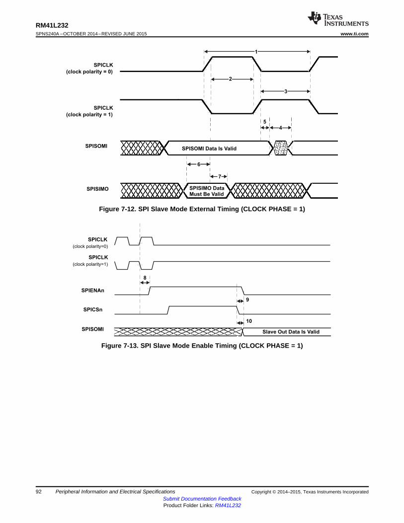
SPISOMISlave Out Data Is Valid
SPICLK
(clock polarity=0)
SPICSn
8
SPICLK
(clock polarity=1)
SPIENAn
9
10
SPISIMO
SPISOMI
5
7
SPISIMO DataMust Be Valid
SPISOMI Data Is Valid
666
SPICLK
(clock polarity = 1)
SPICLK
(clock polarity = 0)
3
2
1
4
RM41L232SPNS240A –OCTOBER 2014–REVISED JUNE 2015 www.ti.com
Figure 7-12. SPI Slave Mode External Timing (CLOCK PHASE = 1)
Figure 7-13. SPI Slave Mode Enable Timing (CLOCK PHASE = 1)
92 Peripheral Information and Electrical Specifications Copyright © 2014–2015, Texas Instruments IncorporatedSubmit Documentation FeedbackProduct Folder Links: RM41L232

EQEPA
VIM EQEPINTn
EQEP
Module
I/O
MUX
CTRL
EQEPENCLK
EQEPIO
EQEPI
VBUSP Interface
VCLK
EQEPB
EQEPIOE
EQEPSO
EQEPS
EQEPSOE
NHETnDIS_SEL
EQEP
CLK
GATE
CDDISx.9
VCLK
ACKCLKSTOP_REQ
SYS_nRST
NHET
VCLK2
nDIS
GIOA[5]
EQEPERR
nEQEPERR
_SYNC
RM41L232www.ti.com SPNS240A –OCTOBER 2014–REVISED JUNE 2015
7.8 Enhanced Quadrature Encoder (eQEP)Figure 7-14 shows the eQEP module interconnections on the device.
Figure 7-14. eQEP Module Interconnections
7.8.1 Clock Enable Control for eQEPx ModulesThe device level control of the eQEP clock is accomplished through the enable/disable of the VCLK clockdomain for eQEP only. This is realized using bit 9 of the CLKDDIS register. The eQEP clock source isenabled by default.
7.8.2 Using eQEPx Phase ErrorThe eQEP module sets the EQEPERR signal output whenever a phase error is detected in its inputsEQEPxA and EQEPxB. This error signal from both the eQEP modules is input to the connection selectionmultiplexor. As shown in Figure 7-14, the output of this selection multiplexor is inverted and connected tothe N2HET module. This connection allows the application to define the response to a phase errorindicated by the eQEP modules.
7.8.3 Input Connections to eQEPx ModulesThe input connections to each of the eQEP modules can be selected between a double-VCLK-synchronized input or a double-VCLK-synchronized and filtered input, as shown in Table 7-17.
Table 7-17. Device-Level Input Synchronization
CONTROL FOR DOUBLE-SYNCHRONIZED CONTROL FOR DOUBLE-SYNCHRONIZEDINPUT SIGNAL CONNECTION TO eQEPx AND FILTERED CONNECTION TO eQEPxeQEPA PINMMR8[0] = 1 PINMMR8[0] = 0 and PINMMR8[1] = 1eQEPB PINMMR8[8] = 1 PINMMR8[8] = 0 and PINMMR8[9] = 1eQEPI PINMMR8[16] = 1 PINMMR8[16] = 0 and PINMMR8[17] = 1eQEPS PINMMR8[24] = 1 PINMMR8[24] = 0 and PINMMR8[25] = 1
Copyright © 2014–2015, Texas Instruments Incorporated Peripheral Information and Electrical Specifications 93Submit Documentation FeedbackProduct Folder Links: RM41L232

RM41L232SPNS240A –OCTOBER 2014–REVISED JUNE 2015 www.ti.com
7.8.4 Enhanced Quadrature Encoder Pulse (eQEPx) Timing
Table 7-18. eQEPx Timing Requirements
PARAMETER TEST CONDITIONS MIN MAX UNITSynchronous 2 tc(VCLK) cycles
tw(QEPP) QEP input periodSynchronous, with input filter 2 tc(VCLK) + filter width cyclesSynchronous 2 tc(VCLK) cycles
tw(INDEXH) QEP Index Input High TimeSynchronous, with input filter 2 tc(VCLK) + filter width cyclesSynchronous 2 tc(VCLK) cycles
tw(INDEXL) QEP Index Input Low TimeSynchronous, with input filter 2 tc(VCLK) + filter width cyclesSynchronous 2 tc(VCLK) cyclestw(STROBH QEP Strobe Input High Time
) Synchronous, with input filter 2 tc(VCLK) + filter width cyclesSynchronous 2 tc(VCLK) cyclestw(STROBL QEP Strobe Input Low Time
) Synchronous, with input filter 2 tc(VCLK) + filter width cycles
Table 7-19. eQEPx Switching Characteristics
PARAMETER MIN MAX UNITtd(CNTR)xin Delay time, external clock to counter increment 4 tc(VCLK) cyclestd(PCS-OUT)QEP Delay time, QEP input edge to position compare sync output 6 tc(VCLK) cycles
94 Peripheral Information and Electrical Specifications Copyright © 2014–2015, Texas Instruments IncorporatedSubmit Documentation FeedbackProduct Folder Links: RM41L232

RM41L232www.ti.com SPNS240A –OCTOBER 2014–REVISED JUNE 2015
8 Device and Documentation Support
8.1 Device Support
8.1.1 Development SupportTexas Instruments (TI) offers an extensive line of development tools for the Hercules™ Safety generationof MCUs, including tools to evaluate the performance of the processors, generate code, develop algorithmimplementations, and fully integrate and debug software and hardware modules.
The following products support development of Hercules™-based applications:
Software Development Tools• Code Composer Studio™ Integrated Development Environment (IDE)
– C/C++ Compiler– Code generation tools– Assembler/Linker– Cycle Accurate Simulator
• Application algorithms• Sample applications code
Hardware Development Tools• Development and evaluation boards• JTAG-based emulators - XDS100™v2, XDS200, XDS560™ v2 emulator• Flash programming tools• Power supply• Documentation and cables
8.1.1.1 Getting Started
This section gives a brief overview of the steps to take when first developing for a RM4x MCU device. Formore detail on each of these steps, see the following:• Initialization of Hercules™ ARM® Cortex®-R4F Microcontrollers (SPNA106)
Copyright © 2014–2015, Texas Instruments Incorporated Device and Documentation Support 95Submit Documentation FeedbackProduct Folder Links: RM41L232

RM 4 1 L 2 3 2 B PZ T R
Prefix:x = Not QualifiedRemoved when qualified
RM = Real Time Microcontroller
CPU:4 = ARM Cortex-R4
Flash / RAM Size:2 = 128KB flash, 32KB RAM Reserved
Reserved
Series Number
Architecture:L = Lockstep
Shipping Options:R = Tape and Reel
Temperature Range:T = –40 C to 105 C
o o
Package Type:PZ = 100-Pin Package
Die Revision:Blank = Die Revision A
B = Die Revision B
RM41L232SPNS240A –OCTOBER 2014–REVISED JUNE 2015 www.ti.com
8.1.2 Device NomenclatureTo designate the stages in the product development cycle, TI assigns prefixes to the part numbers ofall devices.Each device has one of three prefixes: X, P, or null (no prefix) (for example, xRM46L852).These prefixes represent evolutionary stages of product development from engineering prototypesthrough fully qualified production devices/tools.Device development evolutionary flow:
x Experimental device that is not necessarily representative of the final device's electricalspecifications and may not use production assembly flow.
P Prototype device that is not necessarily the final silicon die and may not necessarily meetfinal electrical specifications.
null Fully-qualified production device.x and P devices and TMDX development-support tools are shipped against the following disclaimer:"Developmental product is intended for internal evaluation purposes."Production devices have been characterized fully, and the quality and reliability of the device havebeen demonstrated fully. TI's standard warranty applies.Predictions show that prototype devices have a greater failure rate than the standard productiondevices. Texas Instruments recommends that these devices not be used in any production systembecause their expected end-use failure rate still is undefined. Only qualified production devices are tobe used.
Figure 8-1 illustrates the numbering and symbol nomenclature for the RM41L232.
Figure 8-1. Device Numbering Conventions
96 Device and Documentation Support Copyright © 2014–2015, Texas Instruments IncorporatedSubmit Documentation FeedbackProduct Folder Links: RM41L232

RM41L232www.ti.com SPNS240A –OCTOBER 2014–REVISED JUNE 2015
8.2 Documentation Support
8.2.1 Related Documentation from Texas InstrumentsThe following documents describe the RM41L232 microcontroller.SPNU596 RM41x 16/32-Bit RISC Flash Microcontroller Technical Reference Manual details the integration,
the environment, the functional description, and the programming models for each peripheral andsubsystem in the device.
SPNZ211 RM41L232 Microcontroller, Silicon Revision A, Silicon Errata describes the usage notes andknown exceptions to the functional specifications for the device silicon revision(s).
SPNZ228 RM41L232 Microcontroller, Silicon Revision B, Silicon Errata describes the usage notes andknown exceptions to the functional specifications for the device silicon revision(s).
SPNA207 Calculating Equivalent Power-on-Hours for Hercules™ Safety MCUs details how to use thespreadsheet to calculate the aging effect of temperature on Texas Instruments Hercules Safety MCUs.
8.3 Community ResourcesThe following links connect to TI community resources. Linked contents are provided "AS IS" by therespective contributors. They do not constitute TI specifications and do not necessarily reflect TI's views;see TI's Terms of Use.TI E2E™ Online Community TI's Engineer-to-Engineer (E2E) Community. Created to foster collaboration among
engineers. At e2e.ti.com, you can ask questions, share knowledge, explore ideas and help solveproblems with fellow engineers.
TI Embedded Processors Wiki Texas Instruments Embedded Processors Wiki. Established to help developersget started with Embedded Processors from Texas Instruments and to foster innovation and growth ofgeneral knowledge about the hardware and software surrounding these devices.
8.4 TrademarksHercules, Code Composer Studio, XDS100, XDS560, E2E are trademarks of Texas Instruments.CoreSight is a trademark of ARM Limited.ARM, Cortex are registered trademarks of ARM Limited (or its subsidiaries) in the EU and/or elsewhere.All rights reserved.All other trademarks are the property of their respective owners.
8.5 Electrostatic Discharge CautionThis integrated circuit can be damaged by ESD. Texas Instruments recommends that all integrated circuits be handled withappropriate precautions. Failure to observe proper handling and installation procedures can cause damage.
ESD damage can range from subtle performance degradation to complete device failure. Precision integrated circuits may be moresusceptible to damage because very small parametric changes could cause the device not to meet its published specifications.
8.6 GlossarySLYZ022 — TI Glossary.
This glossary lists and explains terms, acronyms, and definitions.
8.7 Device Identification Code RegisterThe device identification code register identifies several aspects of the device including the silicon version.The details of the device identification code register are shown in Table 8-1. The device identification coderegister value for this device is:• Rev 0 = 0x8048AD05• Rev A = 0x8048AD0D• Rev B = 0x8048AD15
Copyright © 2014–2015, Texas Instruments Incorporated Device and Documentation Support 97Submit Documentation FeedbackProduct Folder Links: RM41L232

RM41L232SPNS240A –OCTOBER 2014–REVISED JUNE 2015 www.ti.com
Figure 8-2. Device ID Bit Allocation Register
31 30 29 28 27 26 25 24 23 22 21 20 19 18 17 16CP-15 UNIQUE ID TECH
R-1 R-00000000100100 R-0
15 14 13 12 11 10 9 8 7 6 5 4 3 2 1 0I/O PERIPH RAMTECH VOLT FLASH ECC VERSION 1 0 1PARITY ECCAGE
R-101 R-0 R-1 R-10 R-1 R-00001 R-1 R-0 R-1LEGEND: R/W = Read/Write; R = Read only; -n = value after reset
Table 8-1. Device ID Bit Allocation Register Field DescriptionsBIT FIELD VALUE DESCRIPTION31 CP15 Indicates the presence of coprocessor 15
1 CP15 present30-17 UNIQUE ID 100100
Silicon version (revision) bits.
This bit field holds a unique number for a dedicated device configuration (die).16-13 TECH Process technology on which the device is manufactured.
0101 F02112 I/O VOLTAGE I/O voltage of the device.
0 I/O are 3.3v11 PERIPHERAL Peripheral Parity
PARITY 1 Parity on peripheral memories10-9 FLASH ECC Flash ECC
10 Program memory with ECC8 RAM ECC Indicates if RAM memory ECC is present.
1 ECC implemented7-3 REVISION 0 Revision of the Device.2-0 FAMILY ID 101 The platform family ID is always 0b101
8.8 Die Identification RegistersThe two die ID registers at addresses 0xFFFFFF7C and 0xFFFFFF80 form a 64-bit die id with theinformation as shown in Table 8-2.
Table 8-2. Die-ID Registers
ITEM NO. OF BITS BIT LOCATIONX Coord. on Wafer 12 0xFFFFFF7C[11:0]Y Coord. on Wafer 12 0xFFFFFF7C[23:12]
Wafer # 8 0xFFFFFF7C[31:24]Lot # 24 0xFFFFFF80[23:0]
Reserved 8 0xFFFFFF80[31:24]
98 Device and Documentation Support Copyright © 2014–2015, Texas Instruments IncorporatedSubmit Documentation FeedbackProduct Folder Links: RM41L232
RM41L232www.ti.com SPNS240A –OCTOBER 2014–REVISED JUNE 2015
8.9 Module CertificationsThe following communications modules have received certification of adherence to a standard.
Copyright © 2014–2015, Texas Instruments Incorporated Device and Documentation Support 99Submit Documentation FeedbackProduct Folder Links: RM41L232
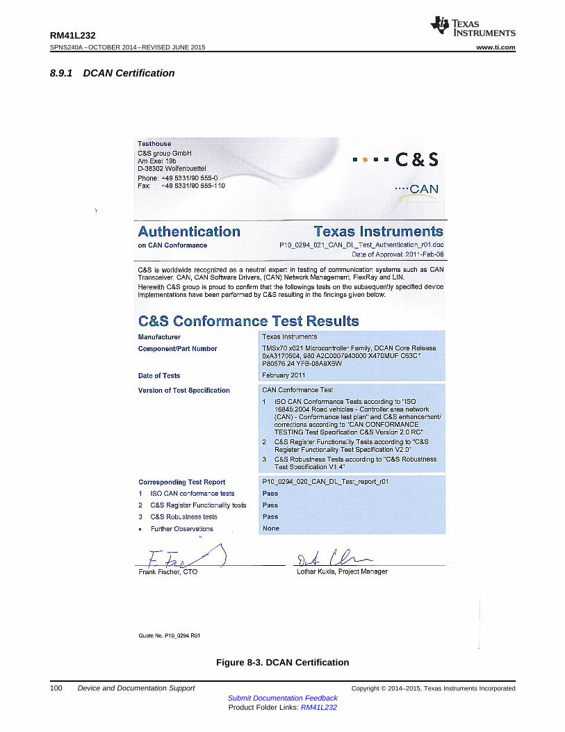
RM41L232SPNS240A –OCTOBER 2014–REVISED JUNE 2015 www.ti.com
8.9.1 DCAN Certification
Figure 8-3. DCAN Certification
100 Device and Documentation Support Copyright © 2014–2015, Texas Instruments IncorporatedSubmit Documentation FeedbackProduct Folder Links: RM41L232
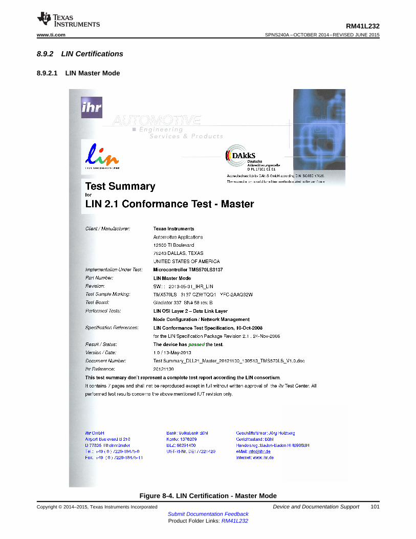
RM41L232www.ti.com SPNS240A –OCTOBER 2014–REVISED JUNE 2015
8.9.2 LIN Certifications
8.9.2.1 LIN Master Mode
Figure 8-4. LIN Certification - Master ModeCopyright © 2014–2015, Texas Instruments Incorporated Device and Documentation Support 101
Submit Documentation FeedbackProduct Folder Links: RM41L232
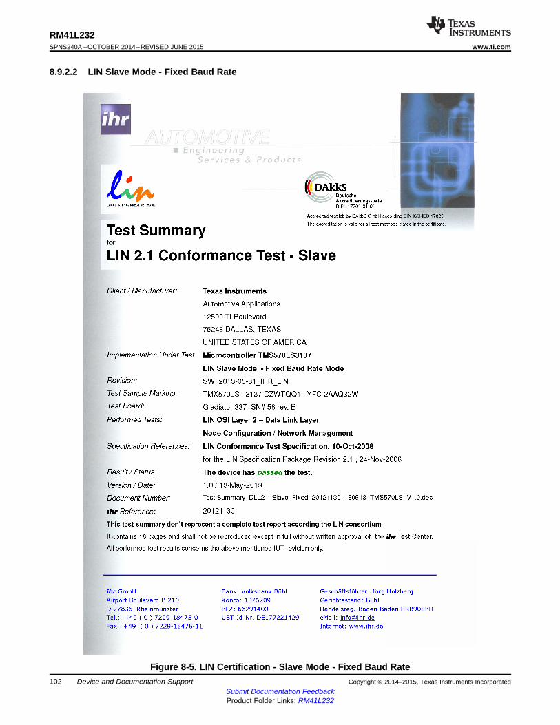
RM41L232SPNS240A –OCTOBER 2014–REVISED JUNE 2015 www.ti.com
8.9.2.2 LIN Slave Mode - Fixed Baud Rate
Figure 8-5. LIN Certification - Slave Mode - Fixed Baud Rate102 Device and Documentation Support Copyright © 2014–2015, Texas Instruments Incorporated
Submit Documentation FeedbackProduct Folder Links: RM41L232

RM41L232www.ti.com SPNS240A –OCTOBER 2014–REVISED JUNE 2015
8.9.2.3 LIN Slave Mode - Adaptive Baud Rate
Figure 8-6. LIN Certification - Slave Mode - Adaptive Baud RateCopyright © 2014–2015, Texas Instruments Incorporated Device and Documentation Support 103
Submit Documentation FeedbackProduct Folder Links: RM41L232
RM41L232SPNS240A –OCTOBER 2014–REVISED JUNE 2015 www.ti.com
9 Mechanical Packaging and Orderable Addendum
9.1 Packaging InformationThe following pages include mechanical packaging and orderable information. This information is the mostcurrent data available for the designated devices. This data is subject to change without notice andrevision of this document. For browser-based versions of this data sheet, refer to the left-hand navigation.
104 Mechanical Packaging and Orderable Addendum Copyright © 2014–2015, Texas Instruments IncorporatedSubmit Documentation FeedbackProduct Folder Links: RM41L232

PACKAGE OPTION ADDENDUM
www.ti.com 28-Jul-2017
Addendum-Page 1
PACKAGING INFORMATION
Orderable Device Status(1)
Package Type PackageDrawing
Pins PackageQty
Eco Plan(2)
Lead/Ball Finish(6)
MSL Peak Temp(3)
Op Temp (°C) Device Marking(4/5)
Samples
RM41L232BPZT ACTIVE LQFP PZ 100 90 Green (RoHS& no Sb/Br)
CU NIPDAU Level-3-260C-168 HR -40 to 105 RM41L232BPZT
(1) The marketing status values are defined as follows:ACTIVE: Product device recommended for new designs.LIFEBUY: TI has announced that the device will be discontinued, and a lifetime-buy period is in effect.NRND: Not recommended for new designs. Device is in production to support existing customers, but TI does not recommend using this part in a new design.PREVIEW: Device has been announced but is not in production. Samples may or may not be available.OBSOLETE: TI has discontinued the production of the device.
(2) RoHS: TI defines "RoHS" to mean semiconductor products that are compliant with the current EU RoHS requirements for all 10 RoHS substances, including the requirement that RoHS substancedo not exceed 0.1% by weight in homogeneous materials. Where designed to be soldered at high temperatures, "RoHS" products are suitable for use in specified lead-free processes. TI mayreference these types of products as "Pb-Free".RoHS Exempt: TI defines "RoHS Exempt" to mean products that contain lead but are compliant with EU RoHS pursuant to a specific EU RoHS exemption.Green: TI defines "Green" to mean the content of Chlorine (Cl) and Bromine (Br) based flame retardants meet JS709B low halogen requirements of <=1000ppm threshold. Antimony trioxide basedflame retardants must also meet the <=1000ppm threshold requirement.
(3) MSL, Peak Temp. - The Moisture Sensitivity Level rating according to the JEDEC industry standard classifications, and peak solder temperature.
(4) There may be additional marking, which relates to the logo, the lot trace code information, or the environmental category on the device.
(5) Multiple Device Markings will be inside parentheses. Only one Device Marking contained in parentheses and separated by a "~" will appear on a device. If a line is indented then it is a continuationof the previous line and the two combined represent the entire Device Marking for that device.
(6) Lead/Ball Finish - Orderable Devices may have multiple material finish options. Finish options are separated by a vertical ruled line. Lead/Ball Finish values may wrap to two lines if the finishvalue exceeds the maximum column width.
Important Information and Disclaimer:The information provided on this page represents TI's knowledge and belief as of the date that it is provided. TI bases its knowledge and belief on informationprovided by third parties, and makes no representation or warranty as to the accuracy of such information. Efforts are underway to better integrate information from third parties. TI has taken andcontinues to take reasonable steps to provide representative and accurate information but may not have conducted destructive testing or chemical analysis on incoming materials and chemicals.TI and TI suppliers consider certain information to be proprietary, and thus CAS numbers and other limited information may not be available for release.
In no event shall TI's liability arising out of such information exceed the total purchase price of the TI part(s) at issue in this document sold by TI to Customer on an annual basis.
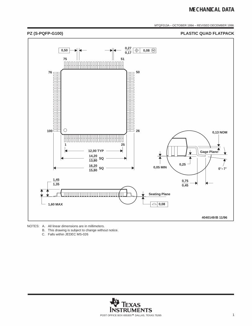
MECHANICAL DATA
MTQF013A – OCTOBER 1994 – REVISED DECEMBER 1996
1POST OFFICE BOX 655303 • DALLAS, TEXAS 75265
PZ (S-PQFP-G100) PLASTIC QUAD FLATPACK
4040149/B 11/96
50
26 0,13 NOM
Gage Plane
0,25
0,450,75
0,05 MIN
0,27
51
25
75
1
12,00 TYP
0,17
76
100
SQ
SQ15,8016,20
13,80
1,351,45
1,60 MAX
14,20
0°–7°
Seating Plane
0,08
0,50 M0,08
NOTES: A. All linear dimensions are in millimeters.B. This drawing is subject to change without notice.C. Falls within JEDEC MS-026

IMPORTANT NOTICE
Texas Instruments Incorporated (TI) reserves the right to make corrections, enhancements, improvements and other changes to itssemiconductor products and services per JESD46, latest issue, and to discontinue any product or service per JESD48, latest issue. Buyersshould obtain the latest relevant information before placing orders and should verify that such information is current and complete.TI’s published terms of sale for semiconductor products (http://www.ti.com/sc/docs/stdterms.htm) apply to the sale of packaged integratedcircuit products that TI has qualified and released to market. Additional terms may apply to the use or sale of other types of TI products andservices.Reproduction of significant portions of TI information in TI data sheets is permissible only if reproduction is without alteration and isaccompanied by all associated warranties, conditions, limitations, and notices. TI is not responsible or liable for such reproduceddocumentation. Information of third parties may be subject to additional restrictions. Resale of TI products or services with statementsdifferent from or beyond the parameters stated by TI for that product or service voids all express and any implied warranties for theassociated TI product or service and is an unfair and deceptive business practice. TI is not responsible or liable for any such statements.Buyers and others who are developing systems that incorporate TI products (collectively, “Designers”) understand and agree that Designersremain responsible for using their independent analysis, evaluation and judgment in designing their applications and that Designers havefull and exclusive responsibility to assure the safety of Designers' applications and compliance of their applications (and of all TI productsused in or for Designers’ applications) with all applicable regulations, laws and other applicable requirements. Designer represents that, withrespect to their applications, Designer has all the necessary expertise to create and implement safeguards that (1) anticipate dangerousconsequences of failures, (2) monitor failures and their consequences, and (3) lessen the likelihood of failures that might cause harm andtake appropriate actions. Designer agrees that prior to using or distributing any applications that include TI products, Designer willthoroughly test such applications and the functionality of such TI products as used in such applications.TI’s provision of technical, application or other design advice, quality characterization, reliability data or other services or information,including, but not limited to, reference designs and materials relating to evaluation modules, (collectively, “TI Resources”) are intended toassist designers who are developing applications that incorporate TI products; by downloading, accessing or using TI Resources in anyway, Designer (individually or, if Designer is acting on behalf of a company, Designer’s company) agrees to use any particular TI Resourcesolely for this purpose and subject to the terms of this Notice.TI’s provision of TI Resources does not expand or otherwise alter TI’s applicable published warranties or warranty disclaimers for TIproducts, and no additional obligations or liabilities arise from TI providing such TI Resources. TI reserves the right to make corrections,enhancements, improvements and other changes to its TI Resources. TI has not conducted any testing other than that specificallydescribed in the published documentation for a particular TI Resource.Designer is authorized to use, copy and modify any individual TI Resource only in connection with the development of applications thatinclude the TI product(s) identified in such TI Resource. NO OTHER LICENSE, EXPRESS OR IMPLIED, BY ESTOPPEL OR OTHERWISETO ANY OTHER TI INTELLECTUAL PROPERTY RIGHT, AND NO LICENSE TO ANY TECHNOLOGY OR INTELLECTUAL PROPERTYRIGHT OF TI OR ANY THIRD PARTY IS GRANTED HEREIN, including but not limited to any patent right, copyright, mask work right, orother intellectual property right relating to any combination, machine, or process in which TI products or services are used. Informationregarding or referencing third-party products or services does not constitute a license to use such products or services, or a warranty orendorsement thereof. Use of TI Resources may require a license from a third party under the patents or other intellectual property of thethird party, or a license from TI under the patents or other intellectual property of TI.TI RESOURCES ARE PROVIDED “AS IS” AND WITH ALL FAULTS. TI DISCLAIMS ALL OTHER WARRANTIES ORREPRESENTATIONS, EXPRESS OR IMPLIED, REGARDING RESOURCES OR USE THEREOF, INCLUDING BUT NOT LIMITED TOACCURACY OR COMPLETENESS, TITLE, ANY EPIDEMIC FAILURE WARRANTY AND ANY IMPLIED WARRANTIES OFMERCHANTABILITY, FITNESS FOR A PARTICULAR PURPOSE, AND NON-INFRINGEMENT OF ANY THIRD PARTY INTELLECTUALPROPERTY RIGHTS. TI SHALL NOT BE LIABLE FOR AND SHALL NOT DEFEND OR INDEMNIFY DESIGNER AGAINST ANY CLAIM,INCLUDING BUT NOT LIMITED TO ANY INFRINGEMENT CLAIM THAT RELATES TO OR IS BASED ON ANY COMBINATION OFPRODUCTS EVEN IF DESCRIBED IN TI RESOURCES OR OTHERWISE. IN NO EVENT SHALL TI BE LIABLE FOR ANY ACTUAL,DIRECT, SPECIAL, COLLATERAL, INDIRECT, PUNITIVE, INCIDENTAL, CONSEQUENTIAL OR EXEMPLARY DAMAGES INCONNECTION WITH OR ARISING OUT OF TI RESOURCES OR USE THEREOF, AND REGARDLESS OF WHETHER TI HAS BEENADVISED OF THE POSSIBILITY OF SUCH DAMAGES.Unless TI has explicitly designated an individual product as meeting the requirements of a particular industry standard (e.g., ISO/TS 16949and ISO 26262), TI is not responsible for any failure to meet such industry standard requirements.Where TI specifically promotes products as facilitating functional safety or as compliant with industry functional safety standards, suchproducts are intended to help enable customers to design and create their own applications that meet applicable functional safety standardsand requirements. Using products in an application does not by itself establish any safety features in the application. Designers mustensure compliance with safety-related requirements and standards applicable to their applications. Designer may not use any TI products inlife-critical medical equipment unless authorized officers of the parties have executed a special contract specifically governing such use.Life-critical medical equipment is medical equipment where failure of such equipment would cause serious bodily injury or death (e.g., lifesupport, pacemakers, defibrillators, heart pumps, neurostimulators, and implantables). Such equipment includes, without limitation, allmedical devices identified by the U.S. Food and Drug Administration as Class III devices and equivalent classifications outside the U.S.TI may expressly designate certain products as completing a particular qualification (e.g., Q100, Military Grade, or Enhanced Product).Designers agree that it has the necessary expertise to select the product with the appropriate qualification designation for their applicationsand that proper product selection is at Designers’ own risk. Designers are solely responsible for compliance with all legal and regulatoryrequirements in connection with such selection.Designer will fully indemnify TI and its representatives against any damages, costs, losses, and/or liabilities arising out of Designer’s non-compliance with the terms and provisions of this Notice.
Mailing Address: Texas Instruments, Post Office Box 655303, Dallas, Texas 75265Copyright © 2017, Texas Instruments Incorporated