rms directpath™, 112/106-db audio stereo dac with 32 … · cpvdd capp cpgnd capm vneg outl outr...
TRANSCRIPT

DOUT
MICIN
PCM1863/5
I2S
BCK
AUXIN
2ch Single Ended
AnalogSensor
- Light Intensity
- Ultrasonic
- Battery Level
LRCK
2ch Single EndedPCM514x
miniDSPs,Filters
Current Segment DAC TPA3130
TPA6120A2
BT Module
MSP430WiLAN chip
LIN
EO
UT
Product
Folder
Sample &Buy
Technical
Documents
Tools &
Software
Support &Community
ReferenceDesign
PCM5141, PCM5142SLAS759B –AUGUST 2012–REVISED JANUARY 2016
PCM514x 2-VRMS DirectPath™, 112/106-dB Audio Stereo DACWith 32-bit, 384-kHz PCM Interface
1 Features 3 DescriptionThe PCM514x devices are a family of monolithic
1• Programmable miniDSPCMOS-integrated circuits that include a stereo digital-• Market-Leading Low Out-of-Band Noise to-analog converter and additional support circuitry in
• Selectable Digital-Filter Latency and Performance a small TSSOP package. The PCM514x uses thelatest generation of TI’s advanced segment-DAC• No DC Blocking Capacitors Requiredarchitecture to achieve excellent dynamic• Integrated Negative Charge Pump performance and improved tolerance to clock jitter.
• Intelligent Muting System; Soft Up or Down RampMembers of the PCM514x family integrate a fullyand Analog Mute For 120-dB Mute SNRprogrammable miniDSP core, allowing developers to• Integrated High-Performance Audio PLL With integrate filters, dynamic range controls, custom
BCK Reference To Generate SCK Internally interpolators, and other differentiating features to their• Accepts 16-, 20-, 24-, And 32-Bit Audio Data products.• PCM Data Formats: I2S, Left-Justified, Right- The PCM514x provides 2.1-VRMS ground centered
Justified, TDM / DSP outputs, allowing designers to eliminate DC-blockingcapacitors on the output, as well as external muting• SPI or I2C Controlcircuits traditionally associated with single-supply line• Software or Hardware Configurationdrivers.
• Automatic Power-Save Mode When LRCK AndThe integrated line driver surpasses all other charge-BCK Are Deactivatedpump-based line drivers by supporting loads down to• 1.8-V or 3.3-V Fail-Safe LVCMOS Digital Inputs 1 kΩ, allowing the PCM514x to drive up to 10
• Single Supply Operation: products in parallel, such as LCD TV, DVDR, and AV3.3-V Analog, 1.8-V or 3.3-V Digital receivers.
• Integrated Power-On Reset The integrated PLL on the device removes therequirement for a system clock (commonly known as• Small 28-pin TSSOP Packagemaster clock), allowing a 3-wire I2S connection andreducing system EMI.2 Applications
• A/V Receivers Device Information• DVD, BD Players DEVICE NAME PACKAGE BODY SIZE (NOM)• HDTV Receivers PCM5141
TSSOP (28) 9.70 mm × 4.40 mm• Applications Requiring 2-VRMS Audio Output PCM5142
.
Simplified System Diagram
1
An IMPORTANT NOTICE at the end of this data sheet addresses availability, warranty, changes, use in safety-critical applications,intellectual property matters and other important disclaimers. PRODUCTION DATA.
PCM5141, PCM5142SLAS759B –AUGUST 2012–REVISED JANUARY 2016 www.ti.com
Table of Contents1 Features .................................................................. 1 9 Application and Implementation ........................ 59
9.1 Application Information............................................ 592 Applications ........................................................... 19.2 Typical Application .................................................. 593 Description ............................................................. 1
10 Power Supply Recommendations ..................... 614 Revision History..................................................... 210.1 Power Supply Distribution and Requirements ...... 615 Device Comparison ............................................... 310.2 Recommended Powerdown Sequence................. 616 Pin Configuration and Functions ......................... 410.3 External Power Sense Undervoltage Protection6.1 Pin Functions ............................................................ 4 Mode ........................................................................ 63
7 Specifications......................................................... 6 10.4 Power-On Reset Function..................................... 657.1 Absolute Maximum Ratings ...................................... 6 10.5 PCM514x Power Modes ....................................... 667.2 ESD Ratings ............................................................ 6 11 Layout................................................................... 677.3 Recommended Operating Conditions....................... 6 11.1 Layout Guidelines ................................................. 677.4 Thermal Information .................................................. 6 11.2 Layout Example .................................................... 677.5 Electrical Characteristics........................................... 7 12 Register Maps...................................................... 687.6 Timing Requirements: SCK Input ........................... 10
12.1 PCM514x Register Map........................................ 687.7 Timing Requirements: PCM Audio Data................. 1013 Device and Documentation Support ............... 1167.8 Timing Requirements: I2S Master .......................... 10
13.1 Development Support ......................................... 1167.9 Timing Requirements: XSMT.................................. 1013.2 Documentation Support ...................................... 1167.10 Switching Characteristics ...................................... 1113.3 Related Links ...................................................... 1167.11 Typical Characteristics .......................................... 1313.4 Community Resources........................................ 1168 Detailed Description ............................................ 1513.5 Trademarks ......................................................... 1168.1 Overview ................................................................. 1513.6 Electrostatic Discharge Caution.......................... 1168.2 Functional Block Diagram ....................................... 1513.7 Glossary .............................................................. 1168.3 Feature Description................................................. 15
14 Mechanical, Packaging, and Orderable8.4 Device Functional Modes........................................ 52 Information ......................................................... 1168.5 Programming........................................................... 58
4 Revision HistoryNOTE: Page numbers for previous revisions may differ from page numbers in the current version.
Changes from Revision A (September 2012) to Revision B Page
• Deleted Internal Pop-Free Control For Sample-Rate Changes Or Clock Halts, ... With Popless Operation ......................... 1• Changed Accepts 16-, 24-, And 32-Bit Audio Data to Accepts 16-, 20-, 24-, And 32-Bit Audio Data ................................... 1• Added Pin Configuration and Functions section, ESD Ratings table, Feature Description section, Device Functional
Modes, Application and Implementation section, Power Supply Recommendations section, Layout section, Deviceand Documentation Support section, and Mechanical, Packaging, and Orderable Information section ............................... 1
• Clarified Pin Functions table................................................................................................................................................... 4• Changed Operating temperature to Operating junction temperature in Absolute Maximum Ratings .................................... 6• Deleted redundant PLL specification in Recommended Operating Conditions .................................................................... 6• Deleted Intelligent clock error... and ...for pop-free performance in the Overview section. ................................................. 15• Added note on instruction cycles to PCM512x Audio Processing........................................................................................ 21• Deleted text The Graphical Development Environment consists of number of Hybrid Flows that can be downloaded
to the device and run on the miniDSP. From: Software ...................................................................................................... 21• Added note on instruction cycles in Fixed Audio Processing Flow (Program 5).................................................................. 35• Changed Ouptut to Output ................................................................................................................................................... 43• Deleted VREF mode provides 2.1Vrms full-scale output at both AVDD levels...................................................................... 43• Clarified clock generation explanation in Reset and System Clock Functions..................................................................... 46• Clarified external SCK discussion in Clock Slave Mode with BCK PLL to Generate Internal Clocks (3-Wire PCM)........... 48• Deleted The PCM514x disables the internal PLL when an external SCK is supplied. ........................................................ 48
2 Submit Documentation Feedback Copyright © 2012–2016, Texas Instruments Incorporated
Product Folder Links: PCM5141 PCM5142

PCM5141, PCM5142www.ti.com SLAS759B –AUGUST 2012–REVISED JANUARY 2016
5 Device Comparison
Table 1. Differences Between PCM514x DevicesPART NUMBER DYNAMIC RANGE SNR THD
PCM5142A 112 dB 112 dB –93 dBPCM5141A 106 dB 106 dB –92 dB
Table 2. Typical Performance (3.3-V Power Supply)PARAMETER PCM5142 / PCM5141SNR 112 / 106 dBDynamic range 112 /106 dBTHD+N at –1 dBFS –93/ –92 dBFull-scale single-ended output 2.1 VRMS (GND center)Normal 8× oversampling digital filter latency 20tSLow latency 8× oversampling digital filter latency 3.5tSSampling frequency 8 kHz to 384 kHzSystem clock multiples (fSCK): 64, 128, 192, 256, 384, Up to 50 MHz512, 768, 1024, 1152, 1536, 2048, 3072
Copyright © 2012–2016, Texas Instruments Incorporated Submit Documentation Feedback 3
Product Folder Links: PCM5141 PCM5142

CPVDD
CAPP
CPGND
CAPM
VNEG
OUTL
OUTR
AVDD
AGND
VCOM
SDA
SCL
GPIO5
GPIO4
1
2
3
4
5
6
7
8
9
10
11
12
13
14
DVDD
DGND
LDOO
XSMT
ADR1
LRCK
DIN
BCK
SCK
GPIO6
MODE2
MODE1
ADR2
GPIO3
28
27
26
25
24
23
22
21
20
19
18
17
16
15
CPVDD
CAPP
CPGND
CAPM
VNEG
OUTL
OUTR
AVDD
AGND
VCOM
MOSI
MC
GPIO5
GPIO4
1
2
3
4
5
6
7
8
9
10
11
12
13
14
DVDD
DGND
LDOO
XSMT
MISO
LRCK
DIN
BCK
SCK
GPIO6
MS
MODE1
GPIO2
GPIO3
28
27
26
25
24
23
22
21
20
19
18
17
16
15
CPVDD
CAPP
CPGND
CAPM
VNEG
OUTL
OUTR
AVDD
AGND
DEMP
ATT2
ATT1
ATT0
MAST
1
2
3
4
5
6
7
8
9
10
11
12
13
14
DVDD
DGND
LDOO
XSMT
FMT
LRCK
DIN
BCK
SCK
FLT
MODE2
MODE1
DOUT
AGNS
28
27
26
25
24
23
22
21
20
19
18
17
16
15
PCM5141, PCM5142SLAS759B –AUGUST 2012–REVISED JANUARY 2016 www.ti.com
6 Pin Configuration and FunctionsRHB Package RHB Package
RHB PackageI2C Mode Hardwired ModeSPI Mode(MODE1 tied to DGND and MODE2 (MODE1 tied to DGND, MODE2 tied
tied to DVDD) (MODE1 tied to DVDD) to DGND)Top View Top View Top View
Table 3. Gain and Attenuation in Hardwired ModeATT PIN CONDITION (ATT2 : ATT1 : ATT0) GAIN AND ATTENUATION LEVEL
( 0 0 0 ) 0 dB( 0 0 1 ) 3 dB( 0 1 0 ) 6 dB( 0 1 1 ) 9 dB( 1 0 0 ) 12 dB( 1 0 1 ) 15 dB( 1 1 0 ) –6 dB( 1 1 1 ) –3 dB
6.1 Pin Functions
PINMODE, NO. I/O DESCRIPTION
NAMEI2C SPI HW
CPVDD 1 1 1 - Charge pump power supply, 3.3 VCAPP 2 2 2 O Charge pump flying capacitor terminal for positive railCPGND 3 3 3 - Charge pump groundCAPM 4 4 4 O Charge pump flying capacitor terminal for negative railVNEG 5 5 5 O Negative charge pump rail terminal for decoupling, –3.3 VOUTL 6 6 6 O Analog output from DAC left channelOUTR 7 7 7 O Analog output from DAC right channelAVDD 8 8 8 - Analog power supply, 3.3 VAGND 9 9 9 - Analog ground
VCOM output (optional mode selected by register; default setting is VREFVCOM 10 10 – O I2C, SPI mode.) When in VREF mode (default), this pin ties to GND. When in VCOM
mode, decoupling capacitor to GND is required.DEMP: De-emphasis control for 44.1-kHz sampling rate: Off (Low) / OnDEMP – – 10 I HW (High)
4 Submit Documentation Feedback Copyright © 2012–2016, Texas Instruments Incorporated
Product Folder Links: PCM5141 PCM5142

PCM5141, PCM5142www.ti.com SLAS759B –AUGUST 2012–REVISED JANUARY 2016
Pin Functions (continued)PIN
MODE, NO. I/O DESCRIPTIONNAME
I2C SPI HWSDA 11 – – I/O I2C Data for I2C (1) (2)
MOSI – 11 – SPI Input data for SPI (2)I
ATT2 – – 11 HW Digital gain and attenuation control pinSCL 12 – – I2C Input clock for I2C(2)
MC – 12 – I SPI Input clock for SPI (2)
ATT1 – – 12 HW Digital gain and attenuation control pinGPIO5 13 13 – I2C, SPI General purpose digital input and output port (3)
I/OATT0 – – 13 HW Digital gain and attenuation control pinGPIO4 14 14 – I2C, SPI General purpose digital input and output port (3)
I/O I2S Master clock select pin : Master (High) BCK/LRCK outputs, Slave (Low)MAST – – 14 HW BCK/LRCK inputsGPIO3 15 15 – I2C, SPI General purpose digital input and output port (3)
I/O Analog gain selector : 0-dB 2-VRMS output (Low), –6-dB 1-VRMS outputAGNS – – 15 HW (High)ADR2 16 – – I2C 2nd LSB address select bit for I2C
I/OGPIO2 – 16 – SPI General purpose digital input and output portDOUT – – 16 O HW General Purpose Output (Low level)
Mode control selection pin (2)
MODE1 = Low, MODE2 = Low : Hardwired modeMODE1 17 17 17 I MODE1 = Low, MODE2 = High: I2C modeMODE1 = High: SPI mode
I2C,MODE2 18 – 18 MODE2HWMS – 18 – I SPI MS pin (chip select for SPI)GPIO6 19 19 – I/O I2C, SPI General purpose digital input and output portFLT – – 19 I HW Filter select : Normal latency (Low) / Low latency (High)SCK 20 20 20 I System clock input (2)
BCK 21 21 21 I/O Audio data bit clock input (slave) or output (master) (2)
DIN 22 22 22 I Audio data input (2)
LRCK 23 23 23 I/O Audio data word clock input (slave) or output (master) (2)
ADR1 24 – – I2C LSB address select bit for I2CPrimary output data for SPI readback. Secondary; general purpose digitalMISO (GPIO1) – 24 – I/O SPI input/output port controlled by register
FMT – – 24 HW Audio format selection : I2S (Low) / Left justified (High)XSMT 25 25 25 I Soft mute control Soft mute (2) (Low) / soft un-mute (High)LDOO 26 26 26 - Internal logic supply rail terminal for decoupling, 1.8 VDGND 27 27 27 - Digital groundDVDD 28 28 28 - Digital power supply, 3.3 V or 1.8 V
(1) Open-drain configuration in out mode.(2) Failsafe LVCMOS Schmitt trigger input.(3) Internal Pulldown
Copyright © 2012–2016, Texas Instruments Incorporated Submit Documentation Feedback 5
Product Folder Links: PCM5141 PCM5142

PCM5141, PCM5142SLAS759B –AUGUST 2012–REVISED JANUARY 2016 www.ti.com
7 Specifications
7.1 Absolute Maximum Ratingsover operating free-air temperature range (unless otherwise noted)
MIN MAX UNITAVDD, CPVDD, DVDD –0.3 3.9
Supply voltage VLDO with DVDD at 1.8 V –0.3 2.25DVDD at 1.8 V –0.3 2.25
Digital input voltage VDVDD at 3.3 V –0.3 3.9
Analog input voltage –0.3 3.9 VOperating junction temperature, TJ –40 130 °CStorage temperature, Tstg –65 150 °C
7.2 ESD RatingsVALUE UNIT
Human-body model (HBM), per ANSI/ESDA/JEDEC JS-001 (1) ±2000ElectrostaticV(ESD) Vdischarge Charged-device model (CDM), per JEDEC specification JESD22-C101 (2) ±750
(1) JEDEC document JEP155 states that 500-V HBM allows safe manufacturing with a standard ESD control process.(2) JEDEC document JEP157 states that 250-V CDM allows safe manufacturing with a standard ESD control process.
7.3 Recommended Operating ConditionsMIN NOM MAX UNIT
VCOM mode 3 3.3 3.46AVDD Analog power supply voltage Referenced to AGND (1) V
VREF mode 3.2 3.3 3.461.8 V DVDD 1.65 1.8 1.95
DVDD Digital power supply voltage Referenced to DGND (1) V3.3 V DVDD 3.1 3.3 3.46
CPVDD Charge pump supply voltage Referenced to CPGND (1) 3.1 3.3 3.46 VMCLK Master clock frequency 50 MHzLOL, LOR Stereo line output load resistance 1 10 kΩCLOUT Digital output load capacitance 10 pFTJ Operating junction temperature –40 130 °C
(1) All grounds on board are tied together; they must not differ in voltage by more than 0.2-V maximum, for any combination of groundsignals.
7.4 Thermal InformationPCM512x
THERMAL METRIC (1) RHB (TSSOP) UNIT32 PINS
RθJA Junction-to-ambient thermal resistance 72.2 °C/WRθJC(top) Junction-to-case(top) thermal resistance 17.5 °C/WRθJB Junction-to-board thermal resistance 35.0 °C/WψJT Junction-to-top characterization parameter 0.4 °C/WψJB Junction-to-board characterization parameter 34.5 °C/W
(1) For more information about trdational and new thermal metrics, see the Semiconductor and IC Package Thermal Metrics applicationreport, SPRA953.
6 Submit Documentation Feedback Copyright © 2012–2016, Texas Instruments Incorporated
Product Folder Links: PCM5141 PCM5142

PCM5141, PCM5142www.ti.com SLAS759B –AUGUST 2012–REVISED JANUARY 2016
7.5 Electrical CharacteristicsTA = 25°C, AVDD = CPVDD = DVDD = 3.3 V, fS = 48 kHz, system clock = 512 fS and 24-bit data (unless otherwise noted).
PARAMETER TEST CONDITIONS MIN TYP MAX UNITResolution 16 24 32 Bits
DIGITAL INPUT/OUTPUTLogic Family: 3.3-V LVCMOS CompatibleVIH Input logic level, high 0.7 × DVDD VVIL Input logic level, low 0.3 × DVDD VIIH Input logic current, high VIN = VDD 10 µAIIL Input logic current, low VIN = 0 V –10 µAVOH Output logic level, high IOH = –4 mA 0.8 × DVDD VVOL Output logic level, low IOL = 4 mA 0.22 × DVDD VLogic Family 1.8-V LVCMOS CompatibleVIH Input logic level, high 0.7 × DVDD VVIL Input logic level, low 0.3 × DVDD VIIH Input logic current, high VIN = VDD 10 µAIIL Input logic current, low VIN = 0 V –10 µAVOH Output logic level, high IOH = –2 mA 0.8 × DVDD VVOL Output logic level, low IOL = 2 mA 0.22 × DVDD VDYNAMIC PERFORMANCE (PCM MODE) (1) (2)
fS = 48 kHz –93 –83THD+N at –1 dB (2) fS = 96 kHz –93 dB
fS = 192 kHz –93EIAJ, A-weighted, fS = 48 kHz 108 112
Dynamic range (2) EIAJ, A-weighted, fS = 96 kHz 112 dBEIAJ, A-weighted, fS = 192 kHz 112EIAJ, A-weighted, fS = 48 kHz 112
Signal-to-noise ratio (2) EIAJ, A-weighted, fS = 96 kHz 112 dBEIAJ, A-weighted, fS = 192 kHz 112EIAJ, A-weighted, fS = 48 kHz 113 123
Signal-to-noise ratio with analog EIAJ, A-weighted, fS = 96 kHz 113 123 dBmute (2) (3)
EIAJ, A-weighted, fS = 192 kHz 113 123fS = 48 kHz 100 / 95 109 / 103
Channel separation fS = 96 kHz 100 / 95 109 / 103 dBfS = 192 kHz 100 / 95 109 / 103
(1) Filter condition: THD+N: 20-Hz HPF, 20-kHz AES17 LPF Dynamic range: 20-Hz HPF, 20-kHz AES17 LPF, A-weighted Signal-to-noiseratio: 20-Hz HPF, 20-kHz AES17 LPF, A-weighted Channel separation: 20-Hz HPF, 20-kHz AES17 LPF Analog performancespecifications are measured using the System Two Cascade™ audio measurement system by Audio Precision™ in the RMS mode.
(2) Output load is 10 kΩ, with 470-Ω output resistor and a 2.2-nF shunt capacitor (see Recommended Output Filter for the PCM514x).(3) Assert XSMT or both L-ch and R-ch PCM data are BPZ
Copyright © 2012–2016, Texas Instruments Incorporated Submit Documentation Feedback 7
Product Folder Links: PCM5141 PCM5142
PCM5141, PCM5142SLAS759B –AUGUST 2012–REVISED JANUARY 2016 www.ti.com
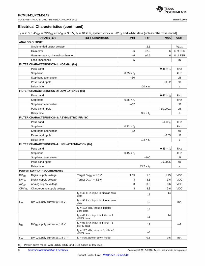
Electrical Characteristics (continued)TA = 25°C, AVDD = CPVDD = DVDD = 3.3 V, fS = 48 kHz, system clock = 512 fS and 24-bit data (unless otherwise noted).
PARAMETER TEST CONDITIONS MIN TYP MAX UNITANALOG OUTPUT
Single-ended output voltage 2.1 VRMS
Gain error –6 ±2.0 6 % of FSRGain mismatch, channel-to-channel –6 ±0.5 6 % of FSRLoad impedance 5 kΩ
FILTER CHARACTERISTICS–1: NORMAL (8x)Pass band 0.45 × fS kHzStop band 0.55 × fS kHzStop band attenuation –60 dBPass-band ripple ±0.02 dBDelay time 20 × tS s
FILTER CHARACTERISTICS–2: LOW LATENCY (8x)Pass band 0.47 × fS kHzStop band 0.55 × fS kHzStop band attenuation –52 dBPass-band ripple ±0.0001 dBDelay time 3.5 × tS s
FILTER CHARACTERISTICS–3: ASYMMETRIC FIR (8x)Pass band 0.4 × fS kHzStop band 0.72 × fS kHzStop band attenuation –52 dBPass-band ripple ±0.05 dBDelay time 1.2 × tS s
FILTER CHARACTERISTICS–4: HIGH-ATTENUATION (8x)Pass band 0.45 × fS kHzStop band 0.45 × fS kHzStop band attenuation –100 dBPass-band ripple ±0.0005 dBDelay time 33.7 × tS s
POWER SUPPLY REQUIREMENTSDVDD Digital supply voltage Target DVDD = 1.8 V 1.65 1.8 1.95 VDCDVDD Digital supply voltage Target DVDD = 3.3 V 3 3.3 3.6 VDCAVDD Analog supply voltage 3 3.3 3.6 VDCCPVDD Charge-pump supply voltage 3 3.3 3.6 VDC
fS = 48 kHz, input is bipolar zero 1411datafS = 96 kHz, input is bipolar zeroIDD DVDD supply current at 1.8 V 12 mAdatafS = 192 kHz, input is bipolar 14zero datafS = 48 kHz, input is 1 kHz – 1 1411dBFS datafS = 96 kHz, input is 1 kHz – 1IDD DVDD supply current at 1.8 V 12 mAdBFS datafS = 192 kHz, input is 1 kHz – 1 14dBFS data
IDD DVDD supply current at 1.8 V (4) fS = N/A, power-down mode 0.3 0.6 mA
(4) Power-down mode, with LRCK, BCK, and SCK halted at low level.
8 Submit Documentation Feedback Copyright © 2012–2016, Texas Instruments Incorporated
Product Folder Links: PCM5141 PCM5142

PCM5141, PCM5142www.ti.com SLAS759B –AUGUST 2012–REVISED JANUARY 2016
Electrical Characteristics (continued)TA = 25°C, AVDD = CPVDD = DVDD = 3.3 V, fS = 48 kHz, system clock = 512 fS and 24-bit data (unless otherwise noted).
PARAMETER TEST CONDITIONS MIN TYP MAX UNITfS = 48 kHz, input is bipolar zero 1512datafS = 96 kHz, input is bipolar zeroIDD DVDD supply current at 3.3 V 13 mAdatafS = 192 kHz, input is bipolar 15zero datafS = 48 kHz, input is 1 kHz – 1 1512dBFS datafS = 96 kHz, input is 1 kHz – 1IDD DVDD supply current at 3.3 V 13 mAdBFS datafS = 192 kHz, input is 1 kHz – 1 15dBFS data
IDD DVDD supply current at 3.3 V (4) fS = N/A, power-down mode 0.5 0.8 mAfS = 48 kHz, input is bipolar zero 1611datafS = 96 kHz, input is bipolar zeroICC AVDD + CPVDD supply current 11 mAdatafS = 192 kHz, input is bipolar 11zero datafS = 48 kHz, input is 1 kHz – 1 3224dBFS datafS = 96 kHz, input is 1 kHz – 1ICC AVDD + CPVDD supply current 24 mAdBFS datafS = 192 kHz, input is 1 kHz – 1 24dBFS data
ICC AVDD + CPVDD supply current (4) fS = N/A, power-down mode 0.2 0.4 mAfS = 48 kHz, input is bipolar zero 7859.4datafS = 96 kHz, input is bipolar zeroPower dissipation, DVDD = 1.8 V 61.2 mWdatafS = 192 kHz, input is bipolar 64.8zero datafS = 48 kHz, input is 1 kHz – 1 130.899dBFS datafS = 96 kHz, input is 1 kHz – 1Power dissipation, DVDD = 1.8 V 100.8 mWdBFS datafS = 192 kHz, input is 1 kHz – 1 104.4dBFS data
Power dissipation, DVDD = 1.8 V (4) fS = N/A, power-down mode 1.2 mWfS = 48 kHz, input is bipolar zero 10379.2datafS = 96 kHz, input is bipolar zeroPower dissipation, DVDD = 3.3 V 82.5 mWdatafS = 192 kHz, input is bipolar 89.1zero datafS = 48 kHz, input is 1 kHz – 1 155118.8dBFS datafS = 96 kHz, input is 1 kHz – 1Power dissipation, DVDD = 3.3 V 122.1 mWdBFS datafS = 192 kHz, input is 1 kHz – 1 128.7dBFS data
Power dissipation, DVDD = 3.3 V (4) fS = N/A, power-down mode 2.3 4 mW
Copyright © 2012–2016, Texas Instruments Incorporated Submit Documentation Feedback 9
Product Folder Links: PCM5141 PCM5142

PCM5141, PCM5142SLAS759B –AUGUST 2012–REVISED JANUARY 2016 www.ti.com
7.6 Timing Requirements: SCK Input
Figure 1 shows the timing requirements for the system clock input. For optimal performance, use a clock source with lowphase jitter and noise.
MIN NOM MAX UNITtSCY System clock pulse cycle time 20 1000 ns
DVDD = 1.8 V 8tSCKH System clock pulse width, high ns
DVDD = 3.3 V 9DVDD = 1.8 V 8
tSCKL System clock pulse width, low nsDVDD = 3.3 V 9
7.7 Timing Requirements: PCM Audio Data
MIN NOM MAX UNITtBCY BCK Pulse Cycle Time 40 nstBCL BCK Pulse Width LOW 16 nstBCH BCK Pulse Width HIGH 16 nstBL BCK Rising Edge to LRCK Edge 8 nstBCK BCK frequency at DVDD = 3.3 V 24.576 MHztBCK(1.8V) BCK frequency at DVDD = 1.8 V 12.288 MHztLB LRCK Edge to BCK Rising Edge 8 nstDS DATA Set Up Time 8 nstDH DATA Hold Time 8 nstDOD DATA delay time from BCK falling edge 15 ns
7.8 Timing Requirements: I2S MasterMIN NOM MAX UNIT
tBCY BCK Pulse Cycle Time 40 nstBCL BCK Pulse Width LOW 16 nstBCH BCK Pulse Width HIGH 16 nstBCK BCK frequency at DVDD = 3.3 V 24.576 MHztBCK(1.8V) BCK frequency at DVDD = 1.8 V 12.288 MHztLRD LRCKx delay time from BCKx falling edge –10 20 nstDS DATA Set Up Time 8 nstDH DATA Hold Time 8 nstDOD DATA delay time from BCK falling edge at DVDD = 3.3 V 15 nstDOD(1.8V) DATA delay time from BCK falling edge at DVDD = 1.8 V 20 ns
7.9 Timing Requirements: XSMTMIN NOM MAX UNIT
tr Rise time 20 nstf Fall time 20 ns
10 Submit Documentation Feedback Copyright © 2012–2016, Texas Instruments Incorporated
Product Folder Links: PCM5141 PCM5142

tSCKH
System Clock (SCK)
tSCKL
"L"
"H"
0.3*DVDD
0.7*DVDD
tSCY
PCM5141, PCM5142www.ti.com SLAS759B –AUGUST 2012–REVISED JANUARY 2016
7.10 Switching Characteristicsover operating free-air temperature range (unless otherwise noted)
PARAMETER TEST CONDITIONS MIN TYP MAX UNITDATA FORMAT (PCM MODE)
I2S, left-justified, right-justified, andAudio data interface format TDMAudio data bit length 16, 20, 24, 32-bit acceptableAudio data format MSB first, twos-complement
fS Sampling frequency (1) 8 384 kHzCLOCKS
64, 128, 192, 256, 384, 512, 768,System clock frequency 1024, 1152, 1536, 2048, or 3072
fSCK, up to 50 MhzClock divider uses fractional divide 6.7 20 MHzD > 0, P=1
PLL input frequency (2)Clock divider uses integer divide 1 20 MHzD = 0, P=1
(1) One sample time is defined as the reciprocal of the sampling frequency. 1 × tS = 1 / fS(2) With the appropriate P coefficient setting, the PLL accepts up to 50 MHz. This clock is then divided to meet the ≤ 20-MHz requirement.
See PLL Calculation.
Figure 1. Timing Requirements for SCK Input
Figure 2. PCM514x Serial Audio Timing - Slave
Copyright © 2012–2016, Texas Instruments Incorporated Submit Documentation Feedback 11
Product Folder Links: PCM5141 PCM5142

PCM5141, PCM5142SLAS759B –AUGUST 2012–REVISED JANUARY 2016 www.ti.com
Figure 3. PCM514x Serial Audio Timing - I2S Master
Figure 4. XSMT Timing for Soft Mute and Soft Un-Mute
12 Submit Documentation Feedback Copyright © 2012–2016, Texas Instruments Incorporated
Product Folder Links: PCM5141 PCM5142

-180
-160
-140
-120
-100
-80
-60
-40
-20
0 5 10 15 20
Frequency (kHz)
Am
plit
ud
e (
dB
)
-180
-160
-140
-120
-100
-80
-60
-40
-20
0 5 10 15 20
Frequency (kHz)
Am
plit
ude (
dB
)
-160
-140
-120
-100
-80
-60
-40
-20
0 5 10 15 20
Frequency (kHz)
Am
plit
ud
e (
dB
)
-160
-140
-120
-100
-80
-60
-40
-20
0 5 10 15 20
Frequency (kHz)
Am
plit
ude (
dB
)
-110
-90
-70
-50
-30
-10
10
-100 -80 -60 -40 -20 0
Input Level (dBFS)
TH
D+
N (
dB
)
-110
-90
-70
-50
-30
-10
10
-100 -80 -60 -40 -20 0
Input Level (dBFS)
TH
D+
N (
dB
)
PCM5141, PCM5142www.ti.com SLAS759B –AUGUST 2012–REVISED JANUARY 2016
7.11 Typical CharacteristicsConsumer grade (non-Q1) devices are specified for TA = 25°C, AVDD = CPVDD = DVDD = 3.3 V, fS = 48 kHz, system clock =512 fS and 24-bit data (unless otherwise noted).
Figure 5. PCM5141 THD+N vs Input Level Figure 6. PCM5142 THD+N vs Input Level
Figure 8. PCM5142 FFT Plot Using a 1-kHz ToneFigure 7. PCM5141 FFT Plot Using a 1-kHz Tone(–60 dBFS) from DC to 20 kHz(–60 dBFS) from DC to 20 kHz
Figure 10. PCM5142 FFT Plot at BPZFigure 9. PCM5141 FFT Plot at Bipolar Zero Data (BPZ)
Copyright © 2012–2016, Texas Instruments Incorporated Submit Documentation Feedback 13
Product Folder Links: PCM5141 PCM5142

-160
-140
-120
-100
-80
-60
-40
-20
0
0 50 100 150 200 250 300
Frequency (kHz)
Am
plit
ude (
dB
)
-160
-140
-120
-100
-80
-60
-40
-20
0
0 50 100 150 200 250 300
Frequency (kHz)
Am
plit
ude (
dB
)
Frequency (kHz)
Am
plit
ude (
dB
)
-180
-160
-140
-120
-100
-80
-60
-40
-20
0 5 10 15 20
Frequency (kHz)
Am
plit
ud
e (
dB
)
PCM5141, PCM5142SLAS759B –AUGUST 2012–REVISED JANUARY 2016 www.ti.com
Typical Characteristics (continued)Consumer grade (non-Q1) devices are specified for TA = 25°C, AVDD = CPVDD = DVDD = 3.3 V, fS = 48 kHz, system clock =512 fS and 24-bit data (unless otherwise noted).
Figure 12. PCM5142 FFT Plot at BPZ With Analog MuteFigure 11. PCM5141 FFT Plot at BPZ With Analog Mute(AMUTE)(AMUTE)
Figure 14. PCM5142 FFT Plot Using a 1-kHz ToneFigure 13. PCM5141 FFT Plot Using a 1-kHz Tone(–60 dBFS) from DC to 300 kHz(–60 dBFS) from DC to 300 kHz
14 Submit Documentation Feedback Copyright © 2012–2016, Texas Instruments Incorporated
Product Folder Links: PCM5141 PCM5142

Audio
Inte
rface
Inte
rpola
tion
Filt
er
32
-bit
∆M
od
ula
tor
Σ
Current
Segment
DAC
I/V
Analo
g
Mute
Zero Data
Detector
PLL
Clock Charge
PumpVComPOR
Clock Halt
Detection
Advanced Mute Control
SCK
BCK
LRCK
CAPP
CAPM
VNEG
XSMT
LINE OUT
DOUT (I2S)
(through
any GPIO)
PCM514x
Pro
gra
mm
able
min
iDS
P
MODE1MS/MODE2MOSI/SDA/ATT2
MC/SCL/ATT1
GPIO6/FLT
MISO/ADR1/FMT
GPIO
Power
Supply
CPVDD (3.3V)
AVDD (3.3V)
DVDD (1.8V or 3.3V)
GND
Program
RAM
Digital
Volume
Control
DIN (I2S)
I/V
Current
Segment
DAC Analo
g
Mute
SPI/I2C
GPIO5/ATT0
GPIO4/MAST
GPIO3/AGNS
GPIO2/ADR2/DOUT
UVP
Soft Mute /
PCM5141, PCM5142www.ti.com SLAS759B –AUGUST 2012–REVISED JANUARY 2016
8 Detailed Description
8.1 OverviewThe integrated PLL on the device provided adds the flexibility to remove the system clock (commonly known asmaster clock), allowing a 3-wire I2S connection and reducing system EMI. In addition, the PLL is completelyprogrammable, allowing the device to become the I2S clock master and drive a DSP serial port as a slave. ThePLL also accepts a non-standard clock (up to 50 MHz) as a source to generate the audio related clock (forexample, 24.576 MHz).
Powersense undervoltage protection utilizes a two-level mute system. Upon clock error or system power failure,the device digitally attenuates the data (or last known good data) and then mutes the analog circuit.
Compared with existing DAC technology, the PCM514x devices offer up to 20-dB lower out-of-band noise,reducing EMI and aliasing in downstream amplifiers/ADCs (from traditional 100-kHz OBN measurements to3 MHz).
The PCM514x devices accept industry-standard audio data formats with 16- to 32-bit data. Sample rates up to384 kHz are supported.
8.2 Functional Block Diagram
8.3 Feature Description
8.3.1 TerminologyControl registers in this data sheet are given by REGISTER BIT/BYTE NAME (Page.x HEX ADDRESS). SErefers to single-ended analog inputs. SCK (System Clock) and MCLK (Master Clock) are used interchangeably.Sampling frequency is symbolized by fS. Full scale is symbolized by FS. Sample time as a unit is symbolized bytS.
Copyright © 2012–2016, Texas Instruments Incorporated Submit Documentation Feedback 15
Product Folder Links: PCM5141 PCM5142

PCM5141, PCM5142SLAS759B –AUGUST 2012–REVISED JANUARY 2016 www.ti.com
Feature Description (continued)8.3.2 Audio Data Interface
8.3.2.1 Audio Serial InterfaceThe audio interface port is a 3-wire serial port with the signals LRCK, BCK, and DIN. BCK is the serial audio bitclock, used to clock the serial data present on DIN into the serial shift register of the audio interface. Serial datais clocked into the PCM514x on the rising edge of BCK. LRCK is the serial audio left/right word clock. LRCKpolarity for left/right is given by the format selected.
Table 4. PCM514x Audio Data Formats, Bit Depths and Clock RatesMAX LRCKCONTROL MODE FORMAT DATA BITS SCK RATE [x fS] BCK RATE [x fS]FREQUENCY [fS]
Up to 192 kHz 128 – 3072 64, 48, 32I2S/LJ 32, 24, 20, 16
384 kHz 64, 128 64, 48, 32Software Control Up to 48 kHz 128 – 3072 128, 256(SPI or I2S)
TDM/DSP 32, 24, 20, 16 96 kHz 128 – 512 128, 256192 kHz 128, 192, 256 128
Up to 192 kHz 128 – 3072 64, 48, 32Hardware Control I2S/LJ 32, 24, 20, 16
384 kHz 64, 128 64, 48, 32
The PCM514x requires the synchronization of LRCK and system clock, but does not need a specific phaserelation between LRCK and system clock.
If the relationship between LRCK and system clock changes more than ±5 SCK, internal operation (using anonchip oscillator) is initialized within one sample period and analog outputs are forced to the bipolar zero leveluntil resynchronization between LRCK and system clock is completed.
If the relationship between LRCK and BCK are invalid more than 4 LRCK periods, internal operation (using anonchip oscillator) is initialized within one sample period and analog outputs are forced to the bipolar zero leveluntil resynchronization between LRCK and BCK is completed.
8.3.2.2 PCM Audio Data FormatsThe PCM514x supports industry-standard audio data formats, including standard I2S and left-justified. Dataformats are selected via Register (Pg0Reg40). All formats require binary twos-complement, MSB-first audio data;up to 32-bit audio data is accepted.
The PCM514x also supports right-justified and TDM/DSP in software control mode. I2S, LJ, RJ, and TDM/DSPare selected using Register (Pg0Reg40). All formats require binary twos-complement, MSB-first audio data. Upto 32 bits are accepted. Default setting is I2S and 24-bit word length.
16 Submit Documentation Feedback Copyright © 2012–2016, Texas Instruments Incorporated
Product Folder Links: PCM5141 PCM5142

!"!#
$ $
! !
!!"!#
!#
!"!#$
!"!#$
!"!$
PCM5141, PCM5142www.ti.com SLAS759B –AUGUST 2012–REVISED JANUARY 2016
Figure 15. Left-Justified Audio Data Format
I2S Data Format; L-channel = LOW, R-channel = HIGH
Figure 16. I2S Audio Data Format
Copyright © 2012–2016, Texas Instruments Incorporated Submit Documentation Feedback 17
Product Folder Links: PCM5141 PCM5142

PCM5141, PCM5142SLAS759B –AUGUST 2012–REVISED JANUARY 2016 www.ti.com
The following data formats are only available in software mode.
Right Justified Data Format; L-channel = HIGH, R-channel = LOW
Figure 17. Right-Justified Audio Data Format
TDM/DSP Data Format; L-channel = FIRST, R-channel = LAST with OFFSET = 0
Figure 18. TDM/DSP 1 Audio Data Format
NOTEIn TDM Modes, Duty Cycle of LRCK should be 1x BCK at minimum. Rising edge isconsidered frame start.
18 Submit Documentation Feedback Copyright © 2012–2016, Texas Instruments Incorporated
Product Folder Links: PCM5141 PCM5142

PCM5141, PCM5142www.ti.com SLAS759B –AUGUST 2012–REVISED JANUARY 2016
TDM/DSP Data Format; L-channel = FIRST, R-channel = LAST with OFFSET = 1
Figure 19. TDM/DSP 2 Audio Data Format
TDM/DSP Data Format; L-channel = FIRST, R-channel = LAST with OFFSET = N
Figure 20. TDM/DSP 3 Audio Data Format
8.3.2.3 Zero Data DetectThe PCM514x has a zero-detect function. When the device detects the continuous zero data for both left andright channels, or separate channels, Analog mutes are set to both OUTL and OUTR, or separate OUTL andOUTR. These are controlled by Page 0, Register 65, D(2:1) as shown in Table 5.
Continuous Zero data cycles are counted by LRCK, and the threshold of decision for analog mute can be set byPage 0, Register 59, D(6:4) for L-ch, and D(2:0) for Rch as shown in Table 6. Default values are 0 for bothchannels.
Copyright © 2012–2016, Texas Instruments Incorporated Submit Documentation Feedback 19
Product Folder Links: PCM5141 PCM5142

PCM5141, PCM5142SLAS759B –AUGUST 2012–REVISED JANUARY 2016 www.ti.com
In Hardware mode, the device uses default values. By default, Both L-ch and R-ch have to be zero data for zerodata detection to begin the muting process etc.
Table 5. Zero Data Detection ModeATMUTECTL VALUE FUNCTION
Independently L-ch or R-ch are zero data for zero data0 detectionBit : 2
Both L-ch and R-ch have to be zero data for zero data1 (Default) detection0 Zero detection and analog mute are disabled for R-ch
Bit : 11 (Default) Zero detection analog mute are enabled for R-ch
0 Zero detection analog mute are disabled for L-chBit : 0
1 (Default) Zero detection analog mute are enabled for L-ch
Table 6. Zero Data Detection TimeATMUTETIML / NUMBER OF LRCKs TIME AT 48 kHzATMUTETIMR
0 0 0 1024 21 ms0 0 1 5120 106 ms0 1 0 10240 213 ms0 1 1 25600 533 ms1 0 0 51200 1.066 sec1 0 1 102400 2.133 sec1 1 0 256000 5.333 sec1 1 1 512000 10.66 sec
8.3.3 XSMT Pin (Soft Mute / Soft Un-Mute)An external digital host controls the PCM514x soft mute function by driving the XSMT pin with a specificminimum rise time (tr) and fall time (tf) for soft mute and soft un-mute. The PCM514x requires tr and tf times ofless than 20 ns. In the majority of applications, this is no problem; however, traces with high capacitance mayhave issues.
When the XSMT pin is shifted from high to low (3.3 V to 0 V), a soft digital attenuation ramp begins. –1-dBattenuation is then applied every sample time from 0 dBFS to –∞. The soft attenuation ramp takes 104 samples.
When the XSMT pin is shifted from low to high (0 V to 3.3 V), a soft digital un-mute is started. 1-dB gain stepsare applied every sample time from –∞ to 0 dBFS. The un-mute takes 104 samples.
In systems where XSMT is not required, it can be directly connected to AVDD.
20 Submit Documentation Feedback Copyright © 2012–2016, Texas Instruments Incorporated
Product Folder Links: PCM5141 PCM5142

PCM5141, PCM5142www.ti.com SLAS759B –AUGUST 2012–REVISED JANUARY 2016
8.3.4 Audio Processing
8.3.4.1 PCM514x Audio Processing Options
8.3.4.1.1 Overview
The PCM514x features a fully-programmable miniDSP core. The algorithms for the miniDSP must be loaded intothe device after power up. The miniDSP has direct access to the digital stereo audio stream, offering thepossibility for advanced DSP algorithms with very low group delay. The miniDSP can run up to 1024 instructionson every audio sample at a 48-kHz sample rate.
NOTEAt higher sampling frequencies, fewer instruction cycles are available. (For example, 512instructions can be done in a 96-kHz frame.)
The PCM514x supports two different code sources. ROM based process flow (See the next section for how toselect) and RAM based process flow. In program 31 (RAM based), different algorithms can be called from ROM -such as EQ, DRC and Zero Crossing volume control. Please see the PurePath Studio Development Environmentfor more details.
8.3.4.1.2 miniDSP Instruction Register
Registers on Page 152-169 are 25-bit instructions for the miniDSP engine. For details, see Table 53. 7 bits ofInstr(32:25) in Base register +0 are reserved bits. 1 bit of Instr(24) - (LSB) in Base register +0 is MSB bit of 25 bitinstruction. These instructions control miniDSP operation. When the fully programmable miniDSP mode isenabled and the DAC channel is powered up, the read and write access to these registers is disabled.
8.3.4.1.3 Digital Output
The PCM514x supports an SDOUT output. This can be selected within the process flow, and driven out of aGPIO pin selected in the register map (for example, Page 0 / Register 80). Users should note that the I2S outputwill be attenuated by 0.5 dB. A full scale (FS) output will actually be FS-0.5dB. This can be compensated forwithin the process flow using PurePath Studio. The I2S output can be a separate audio stream to the analogDAC output, allowing 2.1 and 2.2 systems to be implimented. By default, the SDOUT is not linked to the volumecontrol registers on Page 0 / Register 60, 61, 62. However, it is possible to configure the SDOUT component inPurepath studio to mirror that register.
8.3.4.1.4 Software
Software development for the PCM514x is supported through TI's comprehensive PurePath ™Studio; a powerful,easy-to-use tool designed specifically to simplify software development on the PCM514x miniDSP audioplatform.
Please visit the PCM514x product folder on www.ti.com to learn more about PurePath Console and the lateststatus on available, ready-to-use DSP algorithms.
Copyright © 2012–2016, Texas Instruments Incorporated Submit Documentation Feedback 21
Product Folder Links: PCM5141 PCM5142

PCM5141, PCM5142SLAS759B –AUGUST 2012–REVISED JANUARY 2016 www.ti.com
8.3.4.2 Interpolation FilterThe PCM514x provides 4 types of interpolation filters, selectable by writing to Page 0, Register 43, D(4:0).
Additional RAM based Hybrid Flows can be implemented by selecting Program 31, and downloading instructionsand coefficients to the device.
Table 7. ROM Preset ProgramsPROGRAM D(4:0) DESCRIPTION MINIMUM CYCLESNUMBER
0 0 0000 Reserved1 0 0001 Normal x8/x4/x2/x1 Interpolation Filter (1) 2562 0 0010 Low Latency x8/x4/x2/x1 Interpolation Filter (1) 2563 0 0011 High Attenuation x8/x4/x2 Interpolation Filter (1) 5124 0 0100 Reserved5 0 0101 Preset Process Flow6 0 0110 Reserved7 0 0111 Asymmetric FIR Interpolation Filter (1) 512: : Reserved
31 1 1111 RAM program / Hybrid Flows
(1) At fs=44.1 kHz, de-emphasis filter is supported.
The PCM514x supports four sampling modes (single rate, dual rate, quad rate, and octal rate) which producedifferent oversampling rates (OSR) in the interpolation digital filter operation. These are shown in Table 8.
Table 8. Sampling Modes and Oversampling RatesSAMPLING MODE SAMPLING FREQUENCY (fS) kHz OVERSAMPLING RATE (OSR)
816
Single Rate 32 8 or 1644.148
88.2Dual Rate 4
96176.4
Quad Rate 2192
Octal Rate 384 1 (Bypass)
22 Submit Documentation Feedback Copyright © 2012–2016, Texas Instruments Incorporated
Product Folder Links: PCM5141 PCM5142
−0.05
−0.04
−0.03
−0.02
−0.01
0.00
0.01
0.02
0.03
0.04
0.05
0.0 0.1 0.2 0.3 0.4 0.5
Frequency (x fS)
Am
plit
ud
e (
dB
)
G034
−120
−100
−80
−60
−40
−20
0
0 1 2 3 4
Frequency (x fS)
Am
plit
ud
e (
dB
)
G012
−0.4
−0.2
0.0
0.2
0.4
0.6
0.8
1.0
0 50 100 150 200 250 300 350 400
Samples
Am
plit
ude (
FF
S)
G023
PCM5141, PCM5142www.ti.com SLAS759B –AUGUST 2012–REVISED JANUARY 2016
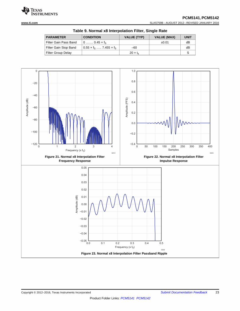
Table 9. Normal x8 Interpolation Filter, Single RatePARAMETER CONDITION VALUE (TYP) VALUE (MAX) UNITFilter Gain Pass Band 0 ……. 0.45 × fS ±0.01 dBFilter Gain Stop Band 0.55 × fS ….. 7.455 × fS –60 dBFilter Group Delay 20 × ts S
SPACE
Figure 21. Normal x8 Interpolation Filter Figure 22. Normal x8 Interpolation FilterFrequency Response Impulse Response
Figure 23. Normal x8 Interpolation Filter Passband Ripple
Copyright © 2012–2016, Texas Instruments Incorporated Submit Documentation Feedback 23
Product Folder Links: PCM5141 PCM5142

−0.05
−0.04
−0.03
−0.02
−0.01
0.00
0.01
0.02
0.03
0.04
0.05
0.0 0.25 0.5
Frequency (x fS)
Am
plit
ude (
dB
)
G031
−120
−100
−80
−60
−40
−20
0
0 1 2
Frequency (x fS)
Am
plit
ud
e (
dB
)
G009
−0.4
−0.2
0.0
0.2
0.4
0.6
0.8
1.0
0 20 40 60 80 100 120 140 160
Samples
Am
plit
ude (
FF
S)
G020
PCM5141, PCM5142SLAS759B –AUGUST 2012–REVISED JANUARY 2016 www.ti.com
Table 10. Normal x4 Interpolation Filter, Dual RatePARAMETER CONDITION VALUE (TYP) VALUE (MAX) UNITFilter Gain Pass Band 0 ……. 0.45 × fS ±0.01 dBFilter Gain Stop Band 0.55 × fS ….. 3.455 × fS –60 dBFilter Group Delay 20 × ts S
SPACE
Figure 24. Normal x4 Interpolation Filter Figure 25. Normal x4 Interpolation FilterFrequency Response Impulse Response
Figure 26. Normal x4 Interpolation Filter Passband Ripple
24 Submit Documentation Feedback Copyright © 2012–2016, Texas Instruments Incorporated
Product Folder Links: PCM5141 PCM5142
−0.05
−0.04
−0.03
−0.02
−0.01
0.00
0.01
0.02
0.03
0.04
0.05
0.0 0.25 0.5
Frequency (x fS)
Am
plit
ud
e (
dB
)
G028
−120
−100
−80
−60
−40
−20
0
0 0.5 1
Frequency (x fS)
Am
plit
ud
e (
dB
)
G006
−0.4
−0.2
0.0
0.2
0.4
0.6
0.8
1.0
0 10 20 30 40 50 60 70 80 90 100
Samples
Am
plit
ude (
FF
S)
G017
PCM5141, PCM5142www.ti.com SLAS759B –AUGUST 2012–REVISED JANUARY 2016
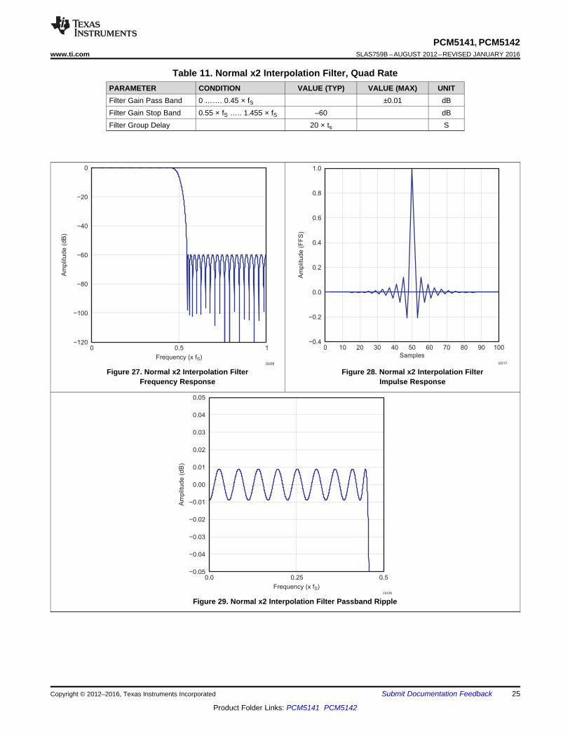
Table 11. Normal x2 Interpolation Filter, Quad RatePARAMETER CONDITION VALUE (TYP) VALUE (MAX) UNITFilter Gain Pass Band 0 ……. 0.45 × fS ±0.01 dBFilter Gain Stop Band 0.55 × fS ….. 1.455 × fS –60 dBFilter Group Delay 20 × ts S
SPACE
Figure 27. Normal x2 Interpolation Filter Figure 28. Normal x2 Interpolation FilterFrequency Response Impulse Response
Figure 29. Normal x2 Interpolation Filter Passband Ripple
Copyright © 2012–2016, Texas Instruments Incorporated Submit Documentation Feedback 25
Product Folder Links: PCM5141 PCM5142

−0.00010
−0.00008
−0.00006
−0.00004
−0.00002
0.00000
0.00002
0.00004
0.00006
0.00008
0.00010
0.0 0.1 0.2 0.3 0.4 0.5
Frequency (x fS)
Am
plit
ude (
dB
)
G033
−120
−100
−80
−60
−40
−20
0
0 1 2 3 4
Frequency (x fS)
Am
plit
ud
e (
dB
)
G011
−0.6
−0.4
−0.2
0.0
0.2
0.4
0.6
0.8
1.0
0 50 100 150 200 250 300 350 400
Samples
Am
plit
ude (
FF
S)
G022
PCM5141, PCM5142SLAS759B –AUGUST 2012–REVISED JANUARY 2016 www.ti.com
Table 12. Low Latency x8 Interpolation Filter, Single RatePARAMETER CONDITION VALUE (TYP) VALUE (MAX) UNITFilter Gain Pass Band 0 ……. 0.45 × fS ±0.001 dBFilter Gain Stop Band 0.55 × fS ….. 7.455 × fS –52 dBFilter Group Delay 3.5 × ts S
SPACE
Figure 30. Low Latency x8 Interpolation Filter Figure 31. Low Latency x8 Interpolation FilterFrequency Response Impulse Response
Figure 32. Low Latency x8 Interpolation Filter Passband Ripple
26 Submit Documentation Feedback Copyright © 2012–2016, Texas Instruments Incorporated
Product Folder Links: PCM5141 PCM5142

−0.0001
−0.00008
−0.00006
−0.00004
−0.00002
0
0.00002
0.00004
0.00006
0.00008
0.0001
0.0 0.25 0.5
Frequency (x fS)
Am
plit
ude (
dB
)
G030
−120
−100
−80
−60
−40
−20
0
0 1 2
Frequency (x fS)
Am
plit
ud
e (
dB
)
G008
−0.6
−0.4
−0.2
0.0
0.2
0.4
0.6
0.8
1.0
0 20 40 60 80 100 120 140 160 180
Samples
Am
plit
ude (
FF
S)
G019
PCM5141, PCM5142www.ti.com SLAS759B –AUGUST 2012–REVISED JANUARY 2016
Table 13. Low Latency x4 Interpolation Filter, Dual RatePARAMETER CONDITION VALUE (TYP) VALUE (MAX) UNITFilter Gain Pass Band 0 ……. 0.45 × fS ±0.001 dBFilter Gain Stop Band 0.55 × fS ….. 3.455 × fS –52 dBFilter Group Delay 3.5 × ts S
SPACE
Figure 33. Low Latency x4 Interpolation Filter Figure 34. Low Latency x4 Interpolation FilterFrequency Response Impulse Response
Figure 35. Low Latency x4 Interpolation Filter Passband Ripple
Copyright © 2012–2016, Texas Instruments Incorporated Submit Documentation Feedback 27
Product Folder Links: PCM5141 PCM5142

−0.0001
−0.00008
−0.00006
−0.00004
−0.00002
0
0.00002
0.00004
0.00006
0.00008
0.0001
0.0 0.25 0.5
Frequency (x fS)
Am
plit
ude (
dB
)
G030
−120
−100
−80
−60
−40
−20
0
0 0.5 1
Frequency (x fS)
Am
plit
ud
e (
dB
)
G005
−0.4
−0.2
0.0
0.2
0.4
0.6
0.8
1.0
0 10 20 30 40 50 60 70 80 90 100
Samples
Am
plit
ude (
FF
S)
G016
PCM5141, PCM5142SLAS759B –AUGUST 2012–REVISED JANUARY 2016 www.ti.com
Table 14. Low Latency ×2 Interpolation Filter, Quad RatePARAMETER CONDITION VALUE (TYP) VALUE (MAX) UNITFilter Gain Pass Band 0 ……. 0.45 × fS ±0.001 dBFilter Gain Stop Band 0.55 × fS ….. 1.455 × fS –52 dBFilter Group Delay 3.5 × ts S
SPACE
Figure 36. Low Latency x2 Interpolation Filter Figure 37. Low Latency x2 Interpolation FilterFrequency Response Impulse Response
Figure 38. Low Latency x2 Interpolation Filter Passband Ripple
28 Submit Documentation Feedback Copyright © 2012–2016, Texas Instruments Incorporated
Product Folder Links: PCM5141 PCM5142

−0.2
−0.15
−0.1
−0.05
0
0.05
0.1
0.15
0.2
0 0.1 0.2 0.3 0.4 0.5Frequency ( × fS)
Am
plitu
de (
dB)
G009
−120
−100
−80
−60
−40
−20
0
0 1 2 3 4Frequency ( × fS)
Am
plitu
de (
dB)
G003
−0.4
−0.2
0
0.2
0.4
0.6
0.8
1
0 10 20 30 40 50 60 70 80Samples
Am
plitu
de (
FF
S)
G006
PCM5141, PCM5142www.ti.com SLAS759B –AUGUST 2012–REVISED JANUARY 2016
Table 15. Asymmetric FIR x8 Interpolation Filter, Single RatePARAMETER CONDITION VALUE (TYP) VALUE (MAX) UNITFilter Gain Pass Band 0 ……. 0.40 × fS ±0.05 dBFilter Gain Stop Band 0.72 × fS ….. 7.28 × fS –50 dBFilter Group Delay 1.2 × ts S
SPACE
Figure 39. Asymmetric FIR x8 Interpolation Filter Figure 40. Asymmetric FIR x8 Interpolation Filter ImpulseFrequency Response, Single Rate Response, Single Rate
Figure 41. Asymmetric FIR x8 Interpolation Filter Passband Ripple, Single Rate
Copyright © 2012–2016, Texas Instruments Incorporated Submit Documentation Feedback 29
Product Folder Links: PCM5141 PCM5142

−0.2
−0.15
−0.1
−0.05
0
0.05
0.1
0.15
0.2
0 0.5 1Frequency ( × fS)
Am
plitu
de (
dB)
G008
−0.4
−0.2
0
0.2
0.4
0.6
0.8
1
0 10 20 30 40 50 60Samples
Am
plitu
de (
FF
S)
G005
−120
−100
−80
−60
−40
−20
0
0 1 2
Am
plit
ud
e (
dB
)
G002Frequency (x fS)
PCM5141, PCM5142SLAS759B –AUGUST 2012–REVISED JANUARY 2016 www.ti.com
Table 16. Asymmetric FIR x4 Interpolation Filter, Dual RatePARAMETER CONDITION VALUE (TYP) VALUE (MAX) UNITFilter Gain Pass Band 0 ……. 0.40 × fS ±0.05 dBFilter Gain Stop Band 0.72 × fS ….. 3.28 × fS –50 dBFilter Group Delay 1.2 × ts S
SPACE
Figure 42. Asymmetric FIR x4 Interpolation Filter Figure 43. Asymmetric FIR x4 Interpolation Filter ImpulseFrequency Response, Dual Rate Response, Dual Rate
Figure 44. Asymmetric x4 Interpolation Filter Passband Ripple, Dual Rate
30 Submit Documentation Feedback Copyright © 2012–2016, Texas Instruments Incorporated
Product Folder Links: PCM5141 PCM5142

−0.2
−0.15
−0.1
−0.05
0
0.05
0.1
0.15
0.2
0 0.25 0.5
Frequency (x f )S
Am
plit
ud
e (
dB
)
G100
−0.4
−0.2
0
0.2
0.4
0.6
0.8
1
0 10 20 30 40 50Samples
Am
plitu
de (
FF
S)
G004
−120
−100
−80
−60
−40
−20
0
0 0.5 1
Am
plit
ude (
dB
)
G001
Frequency (x fS)
PCM5141, PCM5142www.ti.com SLAS759B –AUGUST 2012–REVISED JANUARY 2016
Table 17. Asymmetric FIR x2 Interpolation Filter, Quad RatePARAMETER CONDITION VALUE (TYP) VALUE (MAX) UNITFilter Gain Pass Band 0 ……. 0.40 × fS ±0.05 dBFilter Gain Stop Band 0.72 × fS ….. 1.28 × fS –50 dBFilter Group Delay 1.2 × ts S
SPACE
Figure 45. Asymmetric FIR x2 Interpolation Filter Figure 46. Asymmetric FIR x2 Interpolation Filter ImpulseFrequency Response, Quad Rate Response, Quad Rate
Figure 47. Asymmetric x2 Interpolation Filter Passband Ripple, Quad Rate
Copyright © 2012–2016, Texas Instruments Incorporated Submit Documentation Feedback 31
Product Folder Links: PCM5141 PCM5142

−0.002
−0.0015
−0.001
−0.0005
0
0.0005
0.001
0.0015
0.002
0 0.1 0.2 0.3 0.4 0.5Frequency ( × fS)
Am
plitu
de (
dB)
G009
−120
−100
−80
−60
−40
−20
0
0 1 2 3 4Frequency ( × fS)
Am
plitu
de (
dB)
G003
−0.4
−0.2
0
0.2
0.4
0.6
0.8
1
0 50 100 150 200 250 300 350 400 450 500 550 600Samples
Am
plitu
de (
FF
S)
G006
PCM5141, PCM5142SLAS759B –AUGUST 2012–REVISED JANUARY 2016 www.ti.com
Table 18. High-Attentuation x8 Interpolation Filter, Single RatePARAMETER CONDITION VALUE (TYP) VALUE (MAX) UNITFilter Gain Pass Band 0 ……. 0.45 × fS ±0.0005 dBFilter Gain Stop Band 0.55 × fS ….. 7.455 × fS –100 dBFilter Group Delay 33.7 × tS S
SPACE
Figure 48. High-Attentuation x8 Interpolation Filter Figure 49. High-Attentuation x8 Interpolation Filter ImpulseFrequency Response, Single Rate Response, Single Rate
Figure 50. High-Attentuation x8 Interpolation Filter Passband Ripple, Single Rate
32 Submit Documentation Feedback Copyright © 2012–2016, Texas Instruments Incorporated
Product Folder Links: PCM5141 PCM5142
−0.002
−0.0015
−0.001
−0.0005
0
0.0005
0.001
0.0015
0.002
0 0.25 0.5
Frequency (x fS)
Am
plit
ude (
dB
)
G101
−0.4
−0.2
0
0.2
0.4
0.6
0.8
1
0 50 100 150 200 250 300Samples
Am
plitu
de (
FF
S)
G005
Frequency (x fS)
−120
−100
−80
−60
−40
−20
0
0 1 2
Am
plit
ud
e (
dB
)
G004
PCM5141, PCM5142www.ti.com SLAS759B –AUGUST 2012–REVISED JANUARY 2016
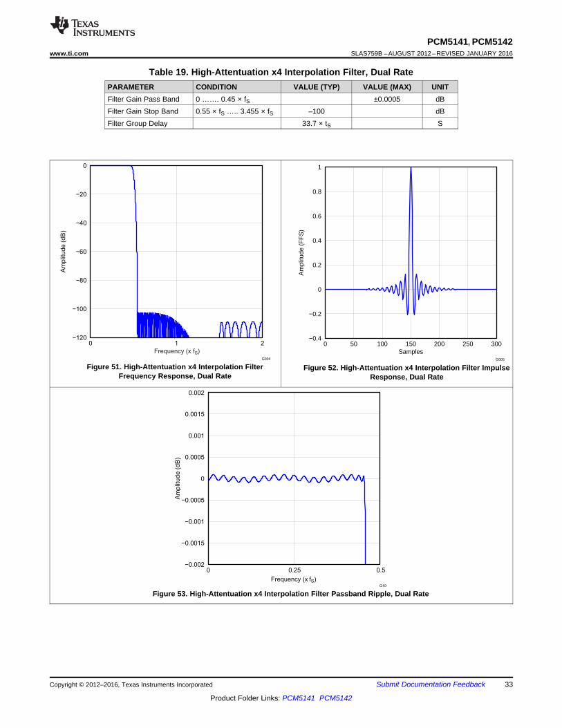
Table 19. High-Attentuation x4 Interpolation Filter, Dual RatePARAMETER CONDITION VALUE (TYP) VALUE (MAX) UNITFilter Gain Pass Band 0 ……. 0.45 × fS ±0.0005 dBFilter Gain Stop Band 0.55 × fS ….. 3.455 × fS –100 dBFilter Group Delay 33.7 × tS S
SPACE
Figure 51. High-Attentuation x4 Interpolation Filter Figure 52. High-Attentuation x4 Interpolation Filter ImpulseFrequency Response, Dual Rate Response, Dual Rate
Figure 53. High-Attentuation x4 Interpolation Filter Passband Ripple, Dual Rate
Copyright © 2012–2016, Texas Instruments Incorporated Submit Documentation Feedback 33
Product Folder Links: PCM5141 PCM5142

−0.002
−0.0015
−0.001
−0.0005
0
0.0005
0.001
0.0015
0.002
0 0.25 0.5
Frequency (x fS)
Am
plit
ud
e (
FF
S)
G102
−0.4
−0.2
0
0.2
0.4
0.6
0.8
1
0 10 20 30 40 50 60 70 80 90 100 110 120Samples
Am
plitu
de (
FF
S)
G004
Frequency (x fS)
−120
−100
−80
−60
−40
−20
0
0 0.5 1
Am
plit
ud
e (
dB
)
G003
PCM5141, PCM5142SLAS759B –AUGUST 2012–REVISED JANUARY 2016 www.ti.com
Table 20. High-Attentuation x2 Interpolation Filter, Quad RatePARAMETER CONDITION VALUE (TYP) VALUE (MAX) UNITFilter Gain Pass Band 0 ……. 0.45 × fS ±0.0005 dBFilter Gain Stop Band 0.55 × fS ….. 1.455 × fS –100 dBFilter Group Delay 33.7 × tS S
SPACE
Figure 54. High-Attentuation x2 Interpolation Filter Figure 55. High-Attentuation x2 Interpolation Filter ImpulseFrequency Response, Quad Rate Response, Quad Rate
Figure 56. High-Attentuation x2 Interpolation Filter Passband Ripple, Quad Rate
34 Submit Documentation Feedback Copyright © 2012–2016, Texas Instruments Incorporated
Product Folder Links: PCM5141 PCM5142

DIN
(1)6 BQ
(2)6 BQ
Lch
Rch
(3)2 BQ
(5)2 BQ
(7)2 BQ
(8)2 BQ
(6)2 BQ
(4)2 BQ
3 Band DRC
Mono Mixer
Stereo Mux
Stereo Mixer
Coeff-1Coeff-2
Master Volume
2ch Interpolation
Filter
1ch I2S out
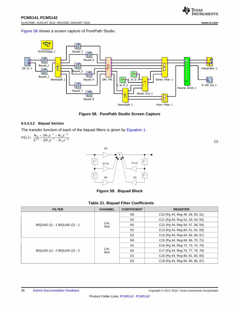
PCM5141, PCM5142www.ti.com SLAS759B –AUGUST 2012–REVISED JANUARY 2016
8.3.4.3 Fixed Audio Processing Flow (Program 5)The PCM514x implements signal processing capabilities and interpolation filtering via processing blocks. Thesefixed processing blocks give users the choice of how much and what type of signal processing they may use andwhich interpolation filter is applied.
The signal processing blocks available are:• Biquad filters• Multiband DRC• Mono mixer• Stereo mixer• Master volume
The addresses of the coefficients are fixed when selecting the fixed processing flow, however, if thesecomponents are used in the RAM source mode (Program 31) the registers for coefficients will change. Users canfind more details in Purepath Studio.
NOTEThis process flow requires 1024 instruction cycles. Therefore, it will only function atsampling frequencies up to 48 kHz.
8.3.4.3.1 Processing Blocks – Detailed Descriptions
Figure 57 shows the fixed processing flow.
Figure 57. Preset Process Flow
Copyright © 2012–2016, Texas Instruments Incorporated Submit Documentation Feedback 35
Product Folder Links: PCM5141 PCM5142
Z-1
Z-1
+
Z-1
Z-1
D1*2
D2
N1*2
N0
N2
( )2
2
1
1
2 3
2
2
1
10
zDzD22
zNzN2NzH
--
--
--
++=
PCM5141, PCM5142SLAS759B –AUGUST 2012–REVISED JANUARY 2016 www.ti.com
Figure 58 shows a screen capture of PurePath Studio.
Figure 58. PurePath Studio Screen Capture
8.3.4.3.2 Biquad Section
The transfer function of each of the biquad filters is given by Equation 1.
(1)
Figure 59. Biquad Block
Table 21. Biquad Filter CoefficientsFILTER CHANNEL COEFFICIENT REGISTER
N0 C10 (Pg 44, Reg 48 ,49, 50, 51)N1 C11 (Pg 44, Reg 52, 53, 54, 55)
Lch,BIQUAD (1) - 1 BIQUAD (2) - 1 N2 C12 (Pg 44, Reg 56, 57, 58, 59)RchD1 C13 (Pg 44, Reg 60, 61, 62, 63)D2 C14 (Pg 44, Reg 64, 65, 66, 67)N0 C15 (Pg 44, Reg 68, 69, 70, 71)N1 C16 (Pg 44, Reg 72, 73, 74, 75)
Lch,BIQUAD (1) - 2 BIQUAD (2) - 2 N2 C17 (Pg 44, Reg 76, 77, 78, 79)RchD1 C18 (Pg 44, Reg 80, 81, 82, 83)D2 C19 (Pg 44, Reg 84, 85, 86, 87)
36 Submit Documentation Feedback Copyright © 2012–2016, Texas Instruments Incorporated
Product Folder Links: PCM5141 PCM5142

PCM5141, PCM5142www.ti.com SLAS759B –AUGUST 2012–REVISED JANUARY 2016
Table 21. Biquad Filter Coefficients (continued)FILTER CHANNEL COEFFICIENT REGISTER
N0 C20 (Pg 44, Reg 88, 89, 90, 91)N1 C21 (Pg 44, Reg 92, 93, 94, 95)
Lch,BIQUAD (1) - 3 BIQUAD (2) - 3 N2 C22 (Pg 44, Reg 96, 97, 98, 99)RchD1 C23 (Pg 44, Reg 100, 101, 102, 103)D2 C24 (Pg 44, Reg 104, 105, 106, 107)N0 C25 (Pg 44, Reg 108, 109, 110, 111)N1 C26 (Pg 44, Reg 112, 113, 114, 115)
Lch,BIQUAD (1) - 4 BIQUAD (2) - 4 N2 C27 (Pg 44, Reg 116, 117, 118, 119)RchD1 C28 (Pg 44, Reg 120, 121, 122, 123)D2 C29 (Pg 44, Reg 124, 125, 126, 127)N0 C30 (Pg 45, Reg 8, 9, 10, 11)N1 C31 (Pg 45, Reg 12, 13, 14, 15)
Lch,BIQUAD (1) - 5 BIQUAD (2) - 5 N2 C32 (Pg 45, Reg 16, 17, 18, 19)RchD1 C33 (Pg 45, Reg 20, 21, 22, 23)D2 C34 (Pg 45, Reg 24, 25, 26, 27)N0 C35 (Pg 45, Reg 28, 29, 30, 31)N1 C36 (Pg 45, Reg 32, 33, 34, 35)
Lch,BIQUAD (1) - 6 BIQUAD (2) - 6 N2 C37 (Pg 45, Reg 36, 37, 38, 39)RchD1 C38 (Pg 45, Reg 40, 41, 42, 43)D2 C39 (Pg 45, Reg 44, 45, 46, 47)N0 C40 (Pg 45, Reg 48, 49, 50, 51)N1 C41 (Pg 45, Reg 52, 53, 54, 55)
Lch,BIQUAD (3) - 1 BIQUAD (4) - 1 N2 C42 (Pg 45, Reg 56, 57, 58, 59)RchD1 C43 (Pg 45, Reg 60, 61, 62, 63)D2 C44 (Pg 45, Reg 64, 65, 66, 67)N0 C45 (Pg 45, Reg 68, 69, 70, 71)N1 C46 (Pg 45, Reg 72, 73, 74, 75)
Lch,BIQUAD (3) - 2 BIQUAD (4) - 2 N2 C47 (Pg 45, Reg 76, 77, 78, 79)RchD1 C48 (Pg 45, Reg 80, 81, 82, 83)D2 C49 (Pg 45, Reg 84, 85, 86, 87)N0 C50 (Pg 45, Reg 88, 89, 90, 91)N1 C51 (Pg 45, Reg 92, 93, 94, 95)
Lch,BIQUAD (5) - 1 BIQUAD (6) - 1 N2 C52 (Pg 45, Reg 96, 97, 98, 99)RchD1 C53 (Pg 45, Reg 100, 101, 102, 103)D2 C54 (Pg 45, Reg 104, 105, 106, 107)N0 C55 (Pg 45, Reg 108, 109, 110, 111)N1 C56 (Pg 45, Reg 112, 113, 114, 115)
Lch,BIQUAD (5) - 2 BIQUAD (6) - 2 N2 C57 (Pg 45, Reg 116, 117, 118, 119)RchD1 C58 (Pg 45, Reg 120, 121, 122, 123)D2 C59 (Pg 45, Reg 124, 125, 126, 127)N0 C60 (Pg 46, Reg 8, 9, 10, 11)N1 C61 (Pg 46, Reg 12, 13, 14, 15)
Lch,BIQUAD (7) - 1 BIQUAD (8) - 1 N2 C62 (Pg 46, Reg 16, 17, 18, 19)RchD1 C63 (Pg 46, Reg 20, 21, 22, 23)D2 C64 (Pg 46, Reg 24, 25, 26, 27)
Copyright © 2012–2016, Texas Instruments Incorporated Submit Documentation Feedback 37
Product Folder Links: PCM5141 PCM5142

PCM5141, PCM5142SLAS759B –AUGUST 2012–REVISED JANUARY 2016 www.ti.com
Table 21. Biquad Filter Coefficients (continued)FILTER CHANNEL COEFFICIENT REGISTER
N0 C65 (Pg 46, Reg 28, 29, 30, 31)N1 C66 (Pg 46, Reg 32, 33, 34, 35)
Lch,BIQUAD (7) - 2 BIQUAD (8) - 2 N2 C67 (Pg 46, Reg 36, 37, 38, 39)RchD1 C68 (Pg 46, Reg 40, 41, 42, 43)D2 C69 (Pg 46, Reg 44, 45, 46, 47)
8.3.4.3.3 Dynamic Range Compression
Dynamic range compression (DRC) improves the overall listening experience. Typical music signals arecharacterized by crest factors (the ratio of peak signal power to average signal power) of 12 dB or more. Toavoid audible distortion due to clipping of peak signals, the gain of the DAC channel must be adjusted so as notto cause hard clipping. As a result, the low applied gain during nominal periods causes the perception that thesignal is not loud enough. To overcome this problem, the DRC in the PCM514x continuously monitors the outputof the DAC Digital Volume control to detect its power level with respect to 0-dB full-scale. When the power levelis low, the DRC increases the input signal gain to make it sound louder, and reduces the gain during peaks toavoid hard clipping. The DRC enables louder audio during nominal periods with a clearer, more pleasantlistening experience.
The 3-band DRC function applies DRC to 3 different mono/stereo signals with 3 different time constants. Thesame DRC curve is applied on all the signals, enabling a multi-band DRC solution. The underlying DRCalgorithm is the same as that available with the DRC component in PurePath Studio. In this instance, the DRCgain acts on each signal in time-multiplexed order, for example, 1-2-3, 1-2-3, 1-2-3.
Table 22. DRC CoefficientsCOEFFICIENT REGISTERDRC_MB_1_DRC_1_DRCAE C70 (Pg 46, Reg 48, 49, 50, 51)DRC_MB_1_DRC_1_DRC1AE C71 (Pg 46, Reg 52, 53, 54, 55)DRC_MB_1_DRC_1_DRCAA C72 (Pg 46, Reg 56, 57, 58, 59)DRC_MB_1_DRC_1_DRC1AA C73 (Pg 46, Reg 60, 61, 62, 63)DRC_MB_1_DRC_1_DRCAD C74 (Pg 46, Reg 64, 65, 66, 67)DRC_MB_1_DRC_1_DRC1AD C75 (Pg 46, Reg 68, 69, 70, 71)DRC_MB_1_DRC_2_DRCAE C76 (Pg 46, Reg 72, 73, 74, 75)DRC_MB_1_DRC_2_DRC1AE C77 (Pg 46, Reg 76, 77, 78, 79)DRC_MB_1_DRC_2_DRCAA C78 (Pg 46, Reg 80, 81, 82, 83)DRC_MB_1_DRC_2_DRC1AA C79 (Pg 46, Reg 84, 85, 86, 87)DRC_MB_1_DRC_2_DRCAD C80 (Pg 46, Reg 88, 89, 90, 91)DRC_MB_1_DRC_2_DRC1AD C81 (Pg 46, Reg 92, 93, 94, 95)DRC_MB_1_DRC_3_DRCAE C82 (Pg 46, Reg 96, 97, 98, 99)DRC_MB_1_DRC_3_DRC1AE C83 (Pg 46, Reg 100, 101, 102, 103)DRC_MB_1_DRC_3_DRCAA C84 (Pg 46, Reg 104, 105, 106, 107)DRC_MB_1_DRC_3_DRC1AA C85 (Pg 46, Reg 108, 109, 119, 111)DRC_MB_1_DRC_3_DRCAD C86 (Pg 46, Reg 112, 113, 114, 115)DRC_MB_1_DRC_3_DRC1AD C87 (Pg 46, Reg 116, 117, 118, 119)DRC_MB_1_DRC_DRCK0 C88 (Pg 46, Reg 120, 121, 122, 123)DRC_MB_1_DRC_DRCK1 C89 (Pg 46, Reg 124, 125, 126, 127)DRC_MB_1_DRC_DRCK2 C90 (Pg 47, Reg 8, 9, 10, 11)DRC_MB_1_DRC_DRCMT1 C91 (Pg 47, Reg 12, 13, 14, 15)DRC_MB_1_DRC_DRCMT2 C92 (Pg 47, Reg 16, 17, 18, 19)DRC_MB_1_DRC_DRCOFF1 C93 (Pg 47, Reg 20, 21, 22, 23)DRC_MB_1_DRC_DRCOFF2 C94 (Pg 47, Reg 24, 25, 26, 27)DRC_MB_1_MinusOne_Q22 C95 (Pg 47, Reg 28, 29, 30, 31)
38 Submit Documentation Feedback Copyright © 2012–2016, Texas Instruments Incorporated
Product Folder Links: PCM5141 PCM5142

PCM5141, PCM5142www.ti.com SLAS759B –AUGUST 2012–REVISED JANUARY 2016
Table 22. DRC Coefficients (continued)COEFFICIENT REGISTERDRC_MB_1_MinusTwo_Q22 C96 (Pg 47, Reg 32, 33, 34, 35)DRC_MB_1_One_M2 C97 (Pg 47, Reg 36, 37, 38, 39)DRC_MB_1_Zero C98 (Pg 47, Reg 40, 41, 42, 43)DRC_MB_1_En_dB C99 (Pg 47, Reg 44, 45, 46, 47)DRC_MB_1_Minus__Zero_dB C100 (Pg 47, Reg 48, 49, 50, 51)DRC_MB_1_60_dB C101 (Pg 47, Reg 52, 53, 54, 55)DRC_MB_1_Minus_60_dB C102 (Pg 47, Reg 56, 57, 58, 59)DRC_MB_1_12_dB C103 (Pg 47, Reg 60, 61, 62, 63)DRC_MB_1_Offset C104 (Pg 47, Reg 64, 65, 66, 67)DRC_MB_1_K C105 (Pg 47, Reg 68, 69, 70, 71)DRC_MB_1_x / DRC_MB_1_DRC C106 (Pg 47, Reg 72, 73, 74, 75)DRC_MB_1_48_dB C107 (Pg 47, Reg 76, 77, 78, 79)DRC_MB_1_Minus_48_dB C108 (Pg 47, Reg 80, 81, 82, 83)DRC_MB_1_c1_3 C109 (Pg 47, Reg 84, 85, 86, 87)DRC_MB_1_c1_2 C110 (Pg 47, Reg 88, 89, 90, 91)DRC_MB_1_c1_1 C111 (Pg 47, Reg 92, 93, 94, 95)DRC_MB_1_c1_0 C112 (Pg 47, Reg 96, 97, 98, 99)DRC_MB_1_O1_1 C113 (Pg 47, Reg 100, 101, 102, 103)DRC_MB_1_S1_1 C114 (Pg 47, Reg 104, 105, 106, 107)DRC_MB_1_O1_2 C115 (Pg 47, Reg 108, 109, 119, 111)DRC_MB_1_S1_2 C116 (Pg 47, Reg 112, 113, 114, 115)DRC_MB_1_O1_3 C117 (Pg 47, Reg 116, 117, 118, 119)DRC_MB_1_S1_3 C118 (Pg 47, Reg 120, 121, 122, 123)DRC_MB_1_One_1_Q17 C119 (Pg 47, Reg 124, 125, 126, 127)DRC_MB_1_Scale1 C120 (Pg 48, Reg 8, 9, 10, 11)DRC_MB_1_x1Coeff C121 (Pg 48, Reg 12, 13, 14, 15)DRC_MB_1_c2_3 C122 (Pg 48, Reg 16, 17, 18, 19)DRC_MB_1_c2_2 C123 (Pg 48, Reg 20, 21, 22, 23)DRC_MB_1_c2_1 C124 (Pg 48, Reg 24, 25, 26, 27)DRC_MB_1_c2_0 C125 (Pg 48, Reg 28, 29, 30, 31)DRC_MB_1_O2_1 C126 (Pg 48, Reg 32, 33, 34, 35)DRC_MB_1_S2_1 C127 (Pg 48, Reg 36, 37, 38, 39)DRC_MB_1_O2_2 C128 (Pg 48, Reg 40, 41, 42, 43)DRC_MB_1_S2_2 C129 (Pg 48, Reg 44, 45, 46, 47)DRC_MB_1_O2_3 C130 (Pg 48, Reg 48, 49, 50, 51)DRC_MB_1_S2_3 C131 (Pg 48, Reg 52, 53, 54, 55)DRC_MB_1_One_2_Q17 C132 (Pg 48, Reg 56, 57, 58, 59)DRC_MB_1_Scale2 C133 (Pg 48, Reg 60, 61, 62, 63)DRC_MB_1_x2Coeff C134 (Pg 48, Reg 64, 65, 66, 67)DRC_MB_1_R1_1 C135 (Pg 48, Reg 68, 69, 70, 71)DRC_MB_1_R1_2 C136 (Pg 48, Reg 72, 73, 74, 75)DRC_MB_1_R2_1 C137 (Pg 48, Reg 76, 77, 78, 79)DRC_MB_1_R2_2 C138 (Pg 48, Reg 80, 81, 82, 83)DRC_MB_1_Band1_GainC C139 (Pg 48, Reg 84, 85, 86, 87)DRC_MB_1_Band2_GainC C140 (Pg 48, Reg 88, 89, 90, 91)DRC_MB_1_Band3_GainC C141 (Pg 48, Reg 92, 93, 94, 95)DRC_MB_1_MinusOne_M1 C142 (Pg 48, Reg 96, 97, 98, 99)
Copyright © 2012–2016, Texas Instruments Incorporated Submit Documentation Feedback 39
Product Folder Links: PCM5141 PCM5142

L1
R1
L2
R2
Select
Lch
Rch
L1
R1
L2
R2
L3
R3
x
x
x
x
x
x
Gain3
Gain2
Gain1
Lch
Rch
( ) ( ) ( )( )å ·= iG ainn,iL_InputnL_O ut
PCM5141, PCM5142SLAS759B –AUGUST 2012–REVISED JANUARY 2016 www.ti.com
Table 22. DRC Coefficients (continued)COEFFICIENT REGISTERDRC_MB_1_One_M1 C143 (Pg 48, Reg 100, 101, 102, 103)DRC_MB_1_Band1_GainE C144 (Pg 48, Reg 104, 105, 106, 107)DRC_MB_1_Band2_GainE C145 (Pg 48, Reg 108, 109, 110, 111)DRC_MB_1_Band3_GainE C146 (Pg 48, Reg 112, 113, 114, 115)DRC_MB_1_minus_One_M2 C147 (Pg 48, Reg 116, 117, 118, 119)
8.3.4.3.4 Stereo Mixer
Three stereo inputs are mixed into one stereo output with input signal gain given by Equation 2.
where• i=1:2,3 (2)
Figure 60 and Table 23 show the stereo mixer operation.
Figure 60. Stereo Mixer Block
Table 23. Stereo Mixer CoefficientsCOEFFICIENT REGISTERStereo_Mixer_1_MixGain1 C148 (Pg 48, Reg 120, 121, 122, 123)Stereo_Mixer_1_MixGain2 C149 (Pg 48, Reg 124, 125, 126, 127)Stereo_Mixer_1_MixGain3 C150 (Pg 49, Reg 8, 9, 10, 11)
8.3.4.3.5 Stereo Multiplexer
The Stereo Multiplexer selects one or two from 4 stereo input channels.
Figure 61. Stereo Multiplexer Block
40 Submit Documentation Feedback Copyright © 2012–2016, Texas Instruments Incorporated
Product Folder Links: PCM5141 PCM5142

Ch-1
Ch-2
x
x
Mono output
Gain1
Gain2
PCM5141, PCM5142www.ti.com SLAS759B –AUGUST 2012–REVISED JANUARY 2016
Table 24. Stereo Multiplexer Select CoefficientCOEFFICIENT REGISTERStereo_Mux_1_MuxSelect C152 (Pg 49, Reg 16, 17, 18, 19)
Table 25. Stereo Multiplexer Input CoefficientCOEFFICIENT REGISTERC_to_D_1_Coefval C153 (Pg 49, Reg 20, 21, 22, 23)C_to_D_2_Coefval
8.3.4.3.6 Mono Mixer
The Mono Mixer computes a weighted sum of 2 input channels and produces an output.
Figure 62. Mono Mixer Block
Table 26. Mono Mixer CoefficientsCOEFFICIENT REGISTERMono_Mixer_1_MixGain1 C154 (Pg 49, Reg 24, 25, 26, 27)Mono_Mixer_1_MixGain2 C155 (Pg 49, Reg 28, 29, 30, 31)
8.3.4.3.7 Master Volume Control
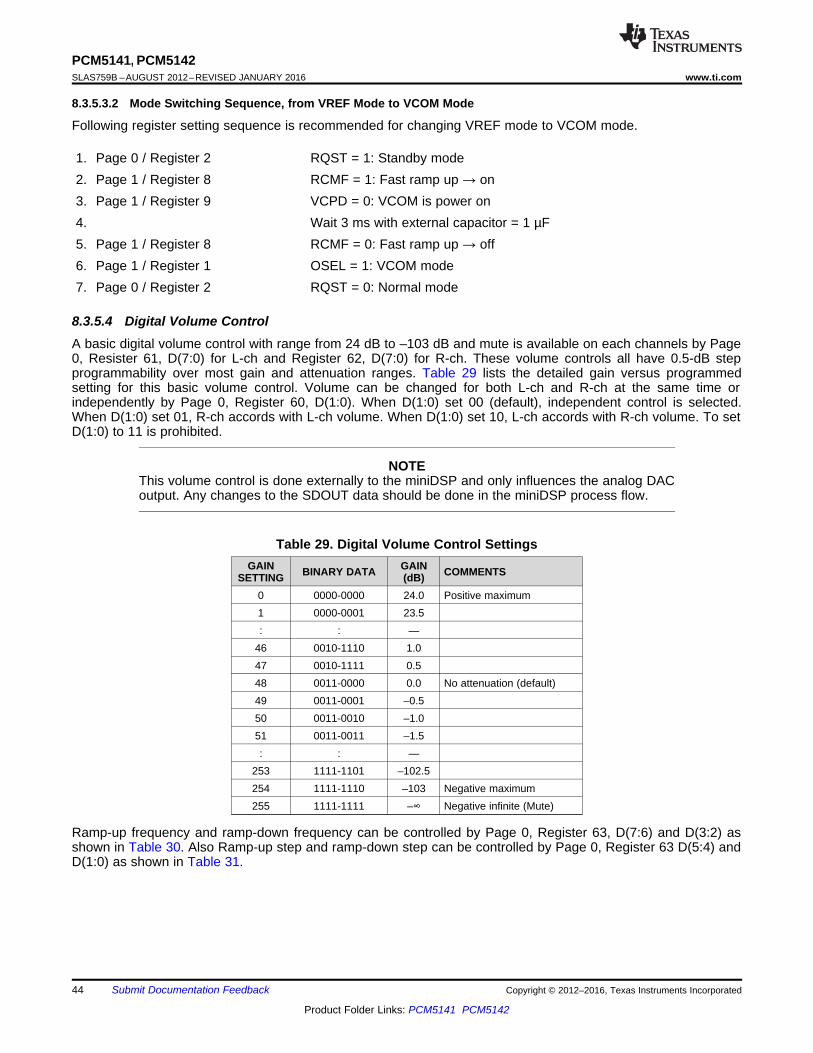
The Master Volume controls the volume using a linear ramp and zero crossing detection for transitions.
Table 27. Mono Mixer CoefficientsCOEFFICIENT REGISTERVolume_ZeroX_1_volcmd C158 (Pg 49, Reg 40, 41, 42, 43)Volume_ZeroX_1_volout C159 (Pg 49, Reg 44, 45, 46, 47)Volume_ZeroX_1_volout_loudness C160 (Pg 49, Reg 48, 49, 50, 51)Volume_ZeroX_1_MinusOne_M2 C161 (Pg 49, Reg 52, 53, 54, 55)Volume_ZeroX_1_workingval_1_pre_CRAM C162 (Pg 49, Reg 56, 57, 58, 59)Volume_ZeroX_1_volout_pre1 C163 (Pg 49, Reg 60, 61, 62, 63)Volume_ZeroX_1_workingval_2_pre_CRAM C164 (Pg 49, Reg 64, 65, 66, 67)Volume_ZeroX_1_volout_pre2 C165 (Pg 49, Reg 68, 69, 70, 71)Volume_ZeroX_1_workingval_3_pre_CRAM C166 (Pg 49, Reg 72, 73, 74, 75)Volume_ZeroX_1_volout_pre3 C167 (Pg 49, Reg 76, 77, 78, 79)Volume_ZeroX_1_One_M2 C168 (Pg 49, Reg 80, 81, 82, 83)Volume_ZeroX_1_Zero C169 (Pg 49, Reg 84, 85, 86, 87)MinusOne_Int C170 (Pg 49, Reg 88, 89, 90, 91)MinusOne_M1 C171 (Pg 49, Reg 92, 93, 94, 95)One_M2 C172 (Pg 49, Reg 96, 97, 98, 99)One_M1 C173 (Pg 49, Reg 100, 101, 102, 103)Zero C174 (Pg 49, Reg 104, 105, 106, 107)
Copyright © 2012–2016, Texas Instruments Incorporated Submit Documentation Feedback 41
Product Folder Links: PCM5141 PCM5142

PCM5141, PCM5142SLAS759B –AUGUST 2012–REVISED JANUARY 2016 www.ti.com
8.3.4.3.8 Miscellaneous Coefficients
Table 28. Miscellaneous CoefficientsCOEFFICIENT REGISTERDRC_MB_1_DataBlock C175 (Pg 49, Reg 108, 109, 110, 111)DRC_MB_1_CoeffBlock C176 (Pg 49, Reg 112, 113, 114, 115)Volume_ZeroX_1_DataBlock C177 (Pg 49, Reg 116, 117, 118, 119)Volume_ZeroX_1_CoeffBlock C178 (Pg 49, Reg 120, 121, 122, 123)plus_one C179 (Pg 49, Reg 124, 125, 126, 127)ADD_OF_filter_in_L C180 (Pg 50, Reg 8, 9, 10, 11)ADD_OF_filter_in_R C181 (Pg 50, Reg 12, 13, 14, 15)
42 Submit Documentation Feedback Copyright © 2012–2016, Texas Instruments Incorporated
Product Folder Links: PCM5141 PCM5142

OUTL
OUTR
470Ω
2.2nF
LINE
OUT
470Ω2.2nF
Output voltage is 2VRMSWith a 10 kΩ Load
PCM5141, PCM5142www.ti.com SLAS759B –AUGUST 2012–REVISED JANUARY 2016
8.3.5 DAC Outputs
8.3.5.1 Analog OutputsThe PCM514x devices include a two-channel DAC, with single-ended outputs. The full-scale output voltage is2.1Vrms with ground center output. A dc-coupled load is supported in addition to an ac-coupled load, if the loadresistance conforms to the specification. The PCM514x DAC outputs on the OUTL and OUTR terminals havemarket-leading low out-of-band noise, which offer up to 20dB lower out-of-band noise compared with existingDAC technology.
Most applications require an external low-pass RC filter (470Ω + 2.2nF) to provide sufficient out-of-band noiserejection. This RC filter provides the added advantage of improved protection against ESD damage.
8.3.5.2 Recommended Output Filter for the PCM514xThe diagram in Figure 63 shows the recommended output filter for the PCM514x. The new PCM514x next-generation current segment architecture offers excellent out-of-band noise, making a traditional 20-kHz low passfilter a thing of the past.
The RC settings below offer a –3-dB filter point at 153 kHz (approximately), giving the DAC the ability toreproduce virtually all frequencies through to it’s maximum sampling rate of 384 kHz. A NP0/C0G type capacitoris strongly recommended for the shunt capacitor for lowest distortion.
Figure 63. Recommended Output Lowpass Filter for 10-kΩ Operation
8.3.5.3 Choosing Between VREF and VCOM ModesVREF mode is the default configuration. This mode allows full 2.1-Vrms signal output. As shown in RecommendedOperating Conditions, the minimum AVDD to avoid clipping is 3.2 V.
VCOM mode allows setting a custom common-mode voltage when required by the application. This somewhatlimits the output signal swing before clipping.
8.3.5.3.1 Voltage Reference and Output Levels
The PCM514x devices have an internal, fixed band-gap reference voltage, with default operation in VREF mode.No external decoupling capacitor is required for this mode.
The PCM514x devices can be operated with a common-mode voltage output (VCOM mode) at the VCOM pin bysetting Page 1, Register 1, D(0) to 1. In this mode, an external decoupling capacitor is required.
When using this DAC in VREF mode, the output-signal voltage is independent of the power-supply voltage: TheD/A conversion gain in VREF mode yields a 2.1-Vrms output voltage with a digital full-scale input. However, inVREF mode, an output waveform may clip due to the limitations that may be present in the analog power supplyvoltage. On the other hand, the full-scale output voltage in VCOM mode is proportional to the analog powersupply AVDD (for example, (2.1 × AVDD / 3.3) Vrms).
Copyright © 2012–2016, Texas Instruments Incorporated Submit Documentation Feedback 43
Product Folder Links: PCM5141 PCM5142
PCM5141, PCM5142SLAS759B –AUGUST 2012–REVISED JANUARY 2016 www.ti.com
8.3.5.3.2 Mode Switching Sequence, from VREF Mode to VCOM Mode
Following register setting sequence is recommended for changing VREF mode to VCOM mode.
1. Page 0 / Register 2 RQST = 1: Standby mode2. Page 1 / Register 8 RCMF = 1: Fast ramp up → on3. Page 1 / Register 9 VCPD = 0: VCOM is power on4. Wait 3 ms with external capacitor = 1 µF5. Page 1 / Register 8 RCMF = 0: Fast ramp up → off6. Page 1 / Register 1 OSEL = 1: VCOM mode7. Page 0 / Register 2 RQST = 0: Normal mode
8.3.5.4 Digital Volume ControlA basic digital volume control with range from 24 dB to –103 dB and mute is available on each channels by Page0, Resister 61, D(7:0) for L-ch and Register 62, D(7:0) for R-ch. These volume controls all have 0.5-dB stepprogrammability over most gain and attenuation ranges. Table 29 lists the detailed gain versus programmedsetting for this basic volume control. Volume can be changed for both L-ch and R-ch at the same time orindependently by Page 0, Register 60, D(1:0). When D(1:0) set 00 (default), independent control is selected.When D(1:0) set 01, R-ch accords with L-ch volume. When D(1:0) set 10, L-ch accords with R-ch volume. To setD(1:0) to 11 is prohibited.
NOTEThis volume control is done externally to the miniDSP and only influences the analog DACoutput. Any changes to the SDOUT data should be done in the miniDSP process flow.
Table 29. Digital Volume Control SettingsGAIN GAINBINARY DATA COMMENTSSETTING (dB)
0 0000-0000 24.0 Positive maximum1 0000-0001 23.5: : —
46 0010-1110 1.047 0010-1111 0.548 0011-0000 0.0 No attenuation (default)49 0011-0001 –0.550 0011-0010 –1.051 0011-0011 –1.5: : —
253 1111-1101 –102.5254 1111-1110 –103 Negative maximum255 1111-1111 –∞ Negative infinite (Mute)
Ramp-up frequency and ramp-down frequency can be controlled by Page 0, Register 63, D(7:6) and D(3:2) asshown in Table 30. Also Ramp-up step and ramp-down step can be controlled by Page 0, Register 63 D(5:4) andD(1:0) as shown in Table 31.
44 Submit Documentation Feedback Copyright © 2012–2016, Texas Instruments Incorporated
Product Folder Links: PCM5141 PCM5142

PCM5141, PCM5142www.ti.com SLAS759B –AUGUST 2012–REVISED JANUARY 2016
Table 30. Ramp-Up or Down FrequencyRAMP-UP RAMP-DOWNEVERY N fS COMMENTS EVERY N fS COMMENTSSPEED FREQUENCY
00 1 Default 00 1 Default01 2 01 210 4 10 411 Direct change 11 Direct change
Table 31. Ramp-Up or Down StepRAMP-UP RAMP-DOWNSTEP dB COMMENTS STEP dB COMMENTSSTEP STEP
00 4.0 00 -4.001 2.0 01 -2.010 1.0 Default 10 -1.0 Default11 0.5 11 -0.5
8.3.5.4.1 Emergency Ramp-Down
Digital volume emergency ramp-down by is provided for situations such as I2S clock error and power supplyfailure. Ramp-down speed is controlled by Page 0, Register 64, D(7:6). Ramp-down step can be controlled byPage 0 Register 64, D(5:4). Default is ramp-down by every fS cycle with –4-dB step.
8.3.5.5 Analog Gain ControlAnalog gain control can be selected between 2-Vrms FS (0dB) or 1-Vrms FS (–6 dB). Gain is controlled throughhardware by the AGNS pin, and through software (SPI/I2C), Page 1, Register 2, D4(L-ch) / D0(R-ch).
Copyright © 2012–2016, Texas Instruments Incorporated Submit Documentation Feedback 45
Product Folder Links: PCM5141 PCM5142
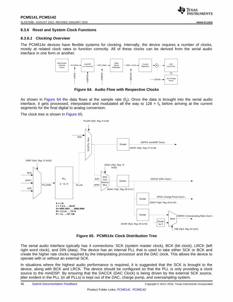
SCK
BCK
SREF (Pg0, Reg 13 0x0D)
PLL
K * R / P
K = J.D
J = 1,2,3,…..,62,63
D= 0000,0001,….,9998,9999
R= 1,2,3,4,….,15,16
P= 1,2,….,127,128
PLLCK
SCK
PLLEN (Pg0, Reg 4 0x04)
SC
K/P
LL
Mux
PLLCKIN
GPIO*
DAC
CLK
Source
Mux
Divider
DividerSCK
GPIO*
DSPCK (miniDSP Clock )
DACCK (DAC Clock )
SDAC (Pg0, Reg 14
0x0E)
DividerCPCK (Charge Pump Clock )
Divider
Divide
by 2
MUX
OSRCK (Oversampling Ratio Clock )
DDSP (Pg0, Reg 27 0x1B)
DDAC (Pg0, Reg 28 0x1C)
DNCP (Pg0, Reg 29 0x1D)
DOSR (Pg0, Reg 30 0x1E)
I16E (Pg0, Reg 34 0x22)
Serial Audio
Interface
(Input)
miniDSP
(inc interpolator)
Delta
Sigma
Modulator
Current
Segments
I V
Line DriverfS (24bit) 16fS (24bit) 128fS (~8 bit) +
DA
CC
K
OS
RC
K
LR
CK
DS
PC
K
-3v3 Charge
PumpCPCK
-3V3
PCM5141, PCM5142SLAS759B –AUGUST 2012–REVISED JANUARY 2016 www.ti.com
8.3.6 Reset and System Clock Functions
8.3.6.1 Clocking OverviewThe PCM514x devices have flexible systems for clocking. Internally, the device requires a number of clocks,mostly at related clock rates to function correctly. All of these clocks can be derived from the serial audiointerface in one form or another.
Figure 64. Audio Flow with Respective Clocks
As shown in Figure 64 the data flows at the sample rate (fS). Once the data is brought into the serial audiointerface, it gets processed, interpolated and modulated all the way to 128 × fS before arriving at the currentsegments for the final digital to analog conversion.
The clock tree is shown in Figure 65.
Figure 65. PCM514x Clock Distribution Tree
The serial audio interface typically has 4 connections: SCK (system master clock), BCK (bit clock), LRCK (leftright word clock), and DIN (data). The device has an internal PLL that is used to take either SCK or BCK andcreate the higher rate clocks required by the interpolating processor and the DAC clock. This allows the device tooperate with or without an external SCK.
In situations where the highest audio performance is required, it is suggested that the SCK is brought to thedevice, along with BCK and LRCK. The device should be configured so that the PLL is only providing a clocksource to the miniDSP. By ensuring that the DACCK (DAC Clock) is being driven by the external SCK source,jitter evident in the PLL (in all PLLs) is kept out of the DAC, charge pump, and oversampling system.46 Submit Documentation Feedback Copyright © 2012–2016, Texas Instruments Incorporated
Product Folder Links: PCM5141 PCM5142

PCM5141, PCM5142www.ti.com SLAS759B –AUGUST 2012–REVISED JANUARY 2016
Everything else should be a division of the incoming SCK. This is done by setting DAC CLK Source Mux (SDACin Figure 65) to use SCK as a source, rather than the output of the SCK/PLL Mux. Code examples for this areavailable in SLASE12.
When the Auto Clock Configuration bit is set (Page 0/ Register 0x25), no additional clocks configuration isrequired. However, when setting custom PLL values and so forth, the target output rates should match thoseshown in the recommended PLL values of Table 132.
8.3.6.2 Clock Slave Mode With Master and System Clock (SCK) Input (4 Wire I2S)The PCM514x requires a system clock to operate the digital interpolation filters and advanced segment DACmodulators. The system clock is applied at the SCK input and supports up to 50 MHz. The PCM514x system-clock detection circuit automatically senses the system-clock frequency. Common audio sampling frequencies inthe bands of 8 kHz, 16 kHz, (32 kHz - 44.1 kHz - 48 kHz), (88.2kHz - 96kHz), (176.4 kHz - 192 kHz), and 384kHz with ±4% tolerance are supported. Values in the parentheses are grouped when detected, (for example,88.2 kHZ and 96 kHz are detected as double rate, and 32 kHz, 44.1 kHz and 48 kHz are detected as singlerate.)
In the presence of a valid bit SCK, BCK and LRCK in software mode, the device will auto-configure the clock treeand PLL to drive the miniDSP as required.
The sampling frequency detector sets the clock for the digital filter, Delta Sigma Modulator (DSM) and theNegative Charge Pump (NCP) automatically. Table 32 shows examples of system clock frequencies for commonaudio sampling rates.
SCK rates that are not common to standard audio clocks, between 1 MHz and 50 MHz, are only supported insoftware mode by configuring various PLL and clock-divider registers. This programmability allows the device tobecome a clock master and drive the host serial port with LRCK and BCK, from a non-audio related clock (forexample, using 12 MHz to generate 44.1 kHz [LRCK] and 2.8224 MHz [BCK]).
Table 32. System Master Clock Inputs for Audio Related ClocksSYSTEM CLOCK FREQUENCY (fSCK) (MHz)SAMPLING
FREQUENCY 64 fS 128 fS 192 fS 256 fS 384 fS 512 fS 768 fS 1024 fS 1152 fS 1536 fS 2048 fS 3072 fS
8 kHz –(1) 1.024 (2) 1.536(2) 2.048 3.072 4.096 6.144 8.192 9.216 12.288 16.384 24.576
16 kHz –(1) 2.048(2) 3.072(2) 4.096 6.144 8.192 12.288 16.384 18.432 24.576 36.864 49.152
32 kHz –(1) 4.096(2) 6.144(2) 8.192 12.288 16.384 24.576 32.768 36.864 49.152 –(1) –(1)
44.1 kHz –(1) 5.6488(2) 8.4672(2) 11.2896 16.9344 22.5792 33.8688 45.1584 –(1) –(1) –(1) –(1)
48 kHz –(1) 6.144(2) 9.216(2) 12.288 18.432 24.576 36.864 49.152 –(1) –(1) –(1) –(1)
88.2 kHz –(1) 11.2896(2) 16.9344 22.5792 33.8688 45.1584 –(1) –(1) –(1) –(1) –(1) –(1)
96 kHz –(1) 12.288(2) 18.432 24.576 36.864 49.152 –(1) –(1) –(1) –(1) –(1) –(1)
176.4 kHz –(1) 22.579 33.8688 45.1584 –(1) –(1) –(1) –(1) –(1) –(1) –(1) –(1)
192 kHz –(1) 24.576 36.864 49.152 –(1) –(1) –(1) –(1) –(1) –(1) –(1) –(1)
384 kHz 24.576 49.152 –(1) –(1) –(1) –(1) –(1) –(1) –(1) –(1) –(1) –(1)
(1) This system clock rate is not supported for the given sampling frequency.(2) This system clock rate is supported by PLL mode.
See Timing Requirements: PCM Audio Data for clock timing requirements.
Copyright © 2012–2016, Texas Instruments Incorporated Submit Documentation Feedback 47
Product Folder Links: PCM5141 PCM5142

PCM5141, PCM5142SLAS759B –AUGUST 2012–REVISED JANUARY 2016 www.ti.com
8.3.6.3 Clock Slave Mode With BCK PLL to Generate Internal Clocks (3-Wire PCM)The system clock PLL mode allows designers to use a simple 3-wire I2S audio source. The 3-wire sourcereduces the need for a high frequency SCK, making PCB layout easier, and reduces high frequencyelectromagnetic interference.
In hardwired mode, the internal PLL is disabled as soon as an external SCK is supplied.
In hardwired mode, the device starts up expecting an external SCK input, but if BCK and LRCK start correctlywhile SCK remains at ground level for 16 successive LRCK periods, then the internal PLL starts, automaticallygenerating an internal SCK from the BCK reference. Specific BCK rates are required to generate an appropriatemaster clock. Table 33 describes the minimum and maximum BCK per LRCK for the integrated PLL toautomatically generate an internal SCK.
In software mode, the user must set all the PLL registers and clock divider registers for referencing BCK. SeeClock Generation Using the PLL for more information. Recommended values can be found in Table 132.
Table 33. BCK Rates (MHz) by LRCK Sample Rate forPCM514x PLL Operation
BCK (fS)SAMPLE F (kHz)
32 648 – –16 – 1.02432 1.024 2.048
44.1 1.4112 2.822448 1.536 3.07296 3.072 6.144192 6.144 12.288384 12.288 24.576
8.3.6.4 Clock Generation Using the PLLThe PCM514x supports a wide range of options to generate the required clocks for the DAC section as well asinterface and other control blocks as shown in Figure 65.
The clocks for the PLL require a source reference clock. This clock is sourced as the incoming BCK or SCK. Insoftware mode, a GPIO can also be used.
The source reference clock for the PLL reference clock is selected by programming the SRCREF value on Page0, Register 13, D(6:4). The PCM514x provides several programmable clock dividers to achieve a variety ofsampling rates for the DAC and clocks for the NCP, OSR, and the miniDSP. OSRCK for OSR must be set at 16fS frequency by DOSR on Page0, Register 30, D(6:0). See Figure 65.
If PLL functionality is not required, set the PLLEN value on Page 0, Register 4, D(0) to 0. In this situation, anexternal SCK is required.
Table 34. PLL Configuration RegistersCLOCK MULTIPLEXER FUNCTION BITS
SRCREF PLL reference Page 0, Register 13, D(6:4)DIVIDER FUNCTION BITS
DDSP miniDSP clock divider Page 0, Register 27, D(6:0)DACCK DAC clock divider Page 0, Register 28, D(6:0)CPCK NCP clock divider Page 0, Register 29, D(6:0)
OSRCK OSR clock divider Page 0, Register 30, D(6:0)DBCK External BCK Div Page 0, Register 32, D(6:0)DLRK External LRCK Div Page 0, Register 33, D(7:0)
48 Submit Documentation Feedback Copyright © 2012–2016, Texas Instruments Incorporated
Product Folder Links: PCM5141 PCM5142
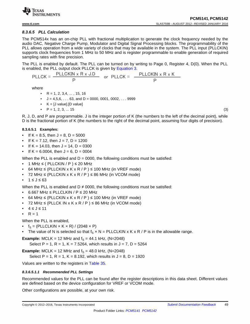
PLLCKIN x R x J.D PLLCK =
PPLLCKIN x R x K
or PLLCK =P
PCM5141, PCM5142www.ti.com SLAS759B –AUGUST 2012–REVISED JANUARY 2016
8.3.6.5 PLL CalculationThe PCM514x has an on-chip PLL with fractional multiplication to generate the clock frequency needed by theaudio DAC, Negative Charge Pump, Modulator and Digital Signal Processing blocks. The programmability of thePLL allows operation from a wide variety of clocks that may be available in the system. The PLL input (PLLCKIN)supports clock frequencies from 1 MHz to 50 MHz and is register programmable to enable generation of requiredsampling rates with fine precision.
The PLL is enabled by default. The PLL can be turned on by writing to Page 0, Register 4, D(0). When the PLLis enabled, the PLL output clock PLLCK is given by Equation 3.
where• R = 1, 2, 3,4, ... , 15, 16• J = 4,5,6, . . . 63, and D = 0000, 0001, 0002, . . . 9999• K = [J value].[D value]• P = 1, 2, 3, ... 15 (3)
R, J, D, and P are programmable. J is the integer portion of K (the numbers to the left of the decimal point), whileD is the fractional portion of K (the numbers to the right of the decimal point, assuming four digits of precision).
8.3.6.5.1 Examples:• If K = 8.5, then J = 8, D = 5000• If K = 7.12, then J = 7, D = 1200• If K = 14.03, then J = 14, D = 0300• If K = 6.0004, then J = 6, D = 0004
When the PLL is enabled and D = 0000, the following conditions must be satisfied:• 1 MHz ≤ ( PLLCKIN / P ) ≤ 20 MHz• 64 MHz ≤ (PLLCKIN x K x R / P ) ≤ 100 MHz (in VREF mode)• 72 MHz ≤ (PLLCKIN x K x R / P ) ≤ 86 MHz (in VCOM mode)• 1 ≤ J ≤ 63
When the PLL is enabled and D ≠ 0000, the following conditions must be satisfied:• 6.667 MHz ≤ PLLCLKIN / P ≤ 20 MHz• 64 MHz ≤ (PLLCKIN x K x R / P ) ≤ 100 MHz (in VREF mode)• 72 MHz ≤ (PLLCK IN x K x R / P ) ≤ 86 MHz (in VCOM mode)• 4 ≤ J ≤ 11• R = 1
When the PLL is enabled,• fS = (PLLCLKIN × K × R) / (2048 × P)• The value of N is selected so that fS × N = PLLCLKIN x K x R / P is in the allowable range.
Example: MCLK = 12 MHz and fS = 44.1 kHz, (N=2048)Select P = 1, R = 1, K = 7.5264, which results in J = 7, D = 5264
Example: MCLK = 12 MHz and fS = 48.0 kHz, (N=2048)Select P = 1, R = 1, K = 8.192, which results in J = 8, D = 1920
Values are written to the registers in Table 35.
8.3.6.5.1.1 Recommended PLL Settings
Recommended values for the PLL can be found after the register descriptions in this data sheet. Different valuesare defined based on the device configuration for VREF or VCOM mode.
Other configurations are possible, at your own risk.
Copyright © 2012–2016, Texas Instruments Incorporated Submit Documentation Feedback 49
Product Folder Links: PCM5141 PCM5142

PCM5141, PCM5142SLAS759B –AUGUST 2012–REVISED JANUARY 2016 www.ti.com
Below are details of the register locations, as well as the nomenclature for the table of registers found at the endof this document.
Table 35. PLL RegistersDIVIDER FUNCTION BITS
PLLE PLL enable Page 0, Register 4, D(0)PPDV PLL P Page 0, Register 20, D(3:0)PJDV PLL J Page 0, Register 21, D(5:0)
Page 0, Register 22, D(5:0)PDDV PLL D
Page 0, Register 23, D(7:0)PRDV PLL R Page 0, Register 24, D(3:0)
Table 36. PLL Configuration RecommendationsCOLUMN DESCRIPTIONfS (kHz) Sampling frequencyRSCK Ratio between sampling frequency and SCK frequency (SCK frequency = RSCK × sampling frequency)SCK (MHz) System master clock frequency at SCK input (pin 20)PLL VCO (MHz) PLL VCO frequency as PLLCK in Figure 65P One of the PLL coefficients in Equation 3PLL REF (MHz) Internal reference clock frequency which is produced by SCK / PM = K * R The final PLL multiplication factor computed from K and R as described in Equation 3K = J.D One of the PLL coefficients in Equation 3R One of the PLL coefficients in Equation 3PLL fS Ratio between fS and PLL VCO frequency (PLL VCO / fS)DSP fS Ratio between miniDSP operating clock rate and fS (PLL fS / NMAC)NMAC The miniDSP clock divider value in Table 34DSP CLK (MHz) The miniDSP operating frequency as DSPCK in Figure 65MOD fS Ratio between DAC operating clock frequency and fS (PLL fS / NDAC)MOD f (kHz) DAC operating frequency as DACCK in Figure 65NDAC DAC clock divider value in Table 34
OSR clock divider value in Table 34 for generating OSRCK in Figure 65. DOSR must be chosen so that MOD fS / DOSRDOSR = 16 for correct operation.NCP NCP (negative charge pump) clock divider value in Table 34CP f Negative charge pump clock frequency (fS × MOD fS / NCP)
Percentage of error between PLL VCO / PLL fS and fS (mismatch error).% Error • This number is typically zero but can be non-zero especially when K is not an integer (D is not zero).
• This number may be non-zero only when the PCM514x acts as a master.
50 Submit Documentation Feedback Copyright © 2012–2016, Texas Instruments Incorporated
Product Folder Links: PCM5141 PCM5142

Divider
Q=1...128
BCKO (Bit Clock Output In Master Mode)
Divider
Q=1...128
LRCKO (LR Clock Output In Master Mode)
Audio Related System Clock(SCK)SCK
BCK
LRCK
PCM5141, PCM5142www.ti.com SLAS759B –AUGUST 2012–REVISED JANUARY 2016
8.3.6.6 Clock Master Mode from Audio Rate Master ClockIn Master Mode, the device generates bit clock (BCK) and left-right clock (LRCK) and outputs them on theappropriate pins. To configure the device in this mode, first put the device into reset, then use registers BCKOand LRKO (Pg 0, Reg 9 0x09). Then reset the LRCK and BCK divider counters using bits RBCK and RLRK (Pg0, Reg 12 0x0C). Finally, exit reset.
An example of this is given in register programming examples in the PCM5242 data sheet (SLASE12.)
Figure 66 shows a simplified serial port clock tree for the device in master mode.
Figure 66. Simplified Clock Tree for SCK Sourced Master Mode
In master mode, SCK is an input and BCK/LRCK are outputs. BCK and LRCK are integer divisions of SCK.Master mode with a non-audio rate master clock source will require external GPIOs to use the PLL in standalonemode.
The PLL will also need to be configured to ensure that the onchip miniDSP processor can be driven at itsmaximum clock rate.
Register changes that need to be done include switching the device into master mode, and setting the dividerratio.
Here is an example of using 24.576 MCLK as a master clock source and driving the BCK and LRCK with integerdividers to create 48 kHz.
In this mode, the DAC section of the device is also running from the PLL output. While the PLL inside thePCM514x is one that has been specified to achieve the stated performance, using the SCK CMOS Oscillatorsource will have less jitter.
To switch the DAC clocks (SDAC in the Figure 65) the following registers should be modified.• Clock Tree Flex Mode (Page 253, Registers 0x3F and 0x40)• DAC and OSR Source Clock Register (Page 0, Reg 14) – set to 0x30 (SCK input, and OSR is set to
whatever the DAC source is)• The DAC clock divider should be 16 FS.
– 16 × 48 kHz = 768 kHz– 24.576 MHz (SCK in) / 768 kHz = 32– Therefor, divide ratio for register DDAC (Page 0, Reg 28 0x1C) should be set to 32. The may the register
is mapped gives 0x00 = 1, so 32 must be converted to 0x1F.
An example configuration can be found in the PCM5242 data sheet (SLASE12).
Copyright © 2012–2016, Texas Instruments Incorporated Submit Documentation Feedback 51
Product Folder Links: PCM5141 PCM5142

PLL
Master Mode
BCK Integer
Divider
Master Mode
LRCK Integer
DividerLRCK OUT
BCK OUT
NEW
AUDIO
SCK
NON AUDIO SCKGPIOx
GPIOy
SCK
BCK
LRCK
PCM5141, PCM5142SLAS759B –AUGUST 2012–REVISED JANUARY 2016 www.ti.com
8.3.6.7 Clock Master from a Non-Audio Rate Master ClockThe classic example here is running a 12-MHz Master clock for a 48-kHz sampling system. Given the clock treefor the device (shown in Figure 65), a non-audio clock rate cannot be brought into the SCK to the PLL in mastermode. Therefore, the PLL source must be configured to be a GPIO pin, and the output brought back into anotherGPIO pin.
Figure 67. Application Diagram for Using Non-Audio Clock Sources to Generate Audio Clocks
The clock flow through the system is shown in Figure 67. The newly-generated SCK must be brought out of thedevice on a GPIO pin, then brought into the SCK pin for integer division to create BCK and LRCK outputs.
NOTEPullup resistors must be used on BCK and LRCK in this mode to ensure the device doesnot go into sleep mode.
A code example for configuring this mode is provided in the PCM5242 data sheet (SLASE12).
8.4 Device Functional Modes
8.4.1 Choosing a Control ModeSPI Mode is selected by connecting MODE1 to DVDD. SPI Mode uses four signal lines and allows higher-speedfull-duplex communication between the host and the PCM514x device.
I2C Mode is selected by connecting MODE1 to DGND and Mode2 to DVDD. I2C uses two signal lines for half-duplex communication, and is widely used in a variety of devices.
Hardware Control Mode is selected by connecting both MODE1 and MODE2 pins to DGND. Hardware control isuseful in applications that do not require on-the-fly device-reconfiguration changes in operating features such asgain or filter latency selection.
See for a comparison of pin assignments for the 28-pin TSSOP.
8.4.1.1 Software Control
8.4.1.1.1 SPI Interface
The SPI interface is a 4-wire synchronous serial port which operates asynchronously to the serial audio interfaceand the system clock (SCK). The serial control interface is used to program and read the on-chip mode registers.
The control interface includes MISO (pin 24), MOSI (pin 11), MC (pin 12), and MS (pin 18). MISO (Master InSlave Out) is the serial data output, used to read back the values of the mode registers; MOSI (Master Out SlaveIn) is the serial data input, used to program the mode registers.
52 Submit Documentation Feedback Copyright © 2012–2016, Texas Instruments Incorporated
Product Folder Links: PCM5141 PCM5142

IDX6 IDX5 IDX4 IDX3 IDX2 IDX1 IDX0 D7 D6 D5 D4 D3 D2 D1 D0
Register Index (or Address) Register Data
MSB LSB
R/W
PCM5141, PCM5142www.ti.com SLAS759B –AUGUST 2012–REVISED JANUARY 2016
Device Functional Modes (continued)MC is the serial bit clock, used to shift data in and out of the control port by falling edge of MC, and MS is themode control enable with LOW active, used to enable the internal mode register access. If feedback from thedevice is not required, the MISO pin can be assigned to GPIO1 by register control.
8.4.1.1.1.1 Register Read and Write Operation
All read/write operations for the serial control port use 16-bit data words. Figure 68 shows the control data wordformat. The most significant bit is the read/write bit. For write operations, the bit must be set to 0. For readoperations, the bit must be set to 1. There are seven bits, labeled IDX[6:0], that hold the register index (oraddress) for the read and write operations. The least significant eight bits, D[7:0], contain the data to be writtento, or the data that was read from, the register specified by IDX[6:0].
Figure 68 and Figure 69 show the functional timing diagram to write or read through the serial control port. MS isheld at a logic-1 state until a register access. To start the register write or read cycle, set MS to logic 0. Sixteenclocks are then provided on MC, corresponding to the 16 bits of the control data word on MOSI and read-backdata on MISO. After the eighth clock cycle has completed, the data from the indexed-mode control registerappears on MISO during the read operation. After the sixteenth clock cycle has completed, the data is latchedinto the indexed-mode control register during the write operation. To write or read subsequent data, MS is set tologic 1 once (see tMHH in Figure 73).
Figure 68. Control Data Word Format; MDI
NOTEB8 is used for selection of Write or Read. Setting = 0 indicates a Write, while = 1 indicatesa Read. Bits 15–9 are used for register address. Bits 7–0 are used for register data.Multiple-byte write or read (up to 8 bytes) is supported while MS is kept low. The addressfield becomes the initial address, automatically incrementing for each byte.
Figure 69. Serial Control Format; Write, Single Byte
Copyright © 2012–2016, Texas Instruments Incorporated Submit Documentation Feedback 53
Product Folder Links: PCM5141 PCM5142
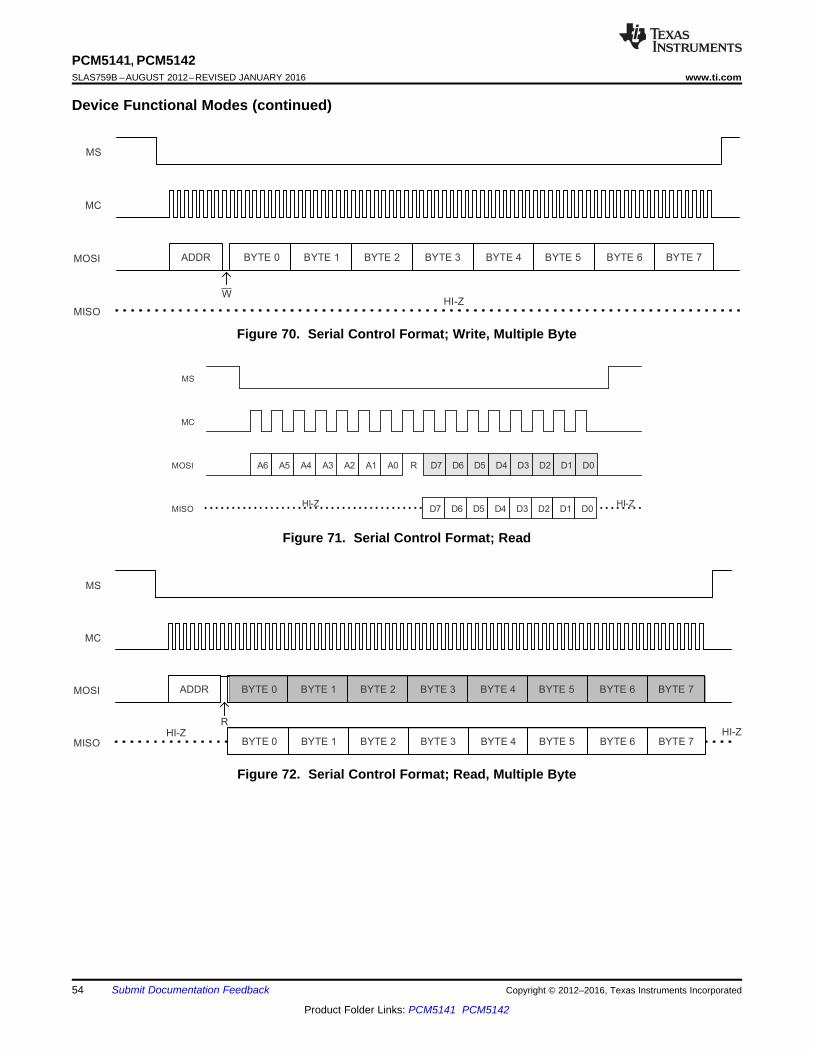
PCM5141, PCM5142SLAS759B –AUGUST 2012–REVISED JANUARY 2016 www.ti.com
Device Functional Modes (continued)
Figure 70. Serial Control Format; Write, Multiple Byte
Figure 71. Serial Control Format; Read
Figure 72. Serial Control Format; Read, Multiple Byte
54 Submit Documentation Feedback Copyright © 2012–2016, Texas Instruments Incorporated
Product Folder Links: PCM5141 PCM5142

PCM5141, PCM5142www.ti.com SLAS759B –AUGUST 2012–REVISED JANUARY 2016
Device Functional Modes (continued)
Figure 73. Control Interface Timing
Table 37. Control Interface TimingMIN MAX UNIT
tMCY MC Pulse Cycle Time 100 nstMCL MC Low Level Time 40 nstMCH MC High Level Time 40 nstMHH MS High Level Time 20 nstMSS MS ↓ Edge to MC ↑ Edge 30 nstMSH MS Hold Time (1) 30 nstMDH MDI Hold Time 15 nstMDS MDI Set-up Time 15 nstMOS MC Rise Edge to MDO Stable 20 ns
(1) MC falling edge for LSB to MS rising edge.
Copyright © 2012–2016, Texas Instruments Incorporated Submit Documentation Feedback 55
Product Folder Links: PCM5141 PCM5142

9
SDA
SCL St
Start condition
1–7 8 1–8 9 1–8 9 9 Sp
Stop condition
Slave address R/W ACK DATA ACK DATA ACK ACK
R/W: Read operation if 1; otherwise, write operation ACK: Acknowledgement of a byte if 0 DATA: 8 bits (byte)
MSB LSB
INC A6 A5 A4 A3 A2 A1 A0
PCM5141, PCM5142SLAS759B –AUGUST 2012–REVISED JANUARY 2016 www.ti.com
8.4.1.1.2 I2C Interface
The PCM514x supports the I2C serial bus and the data transmission protocol for standard and fast mode as aslave device.
In I2C mode, the control terminals are changed as follows.
Table 38. I2C Pins and FunctionsSIGNAL PIN I/O DESCRIPTION
SDA 11 I/O I2C dataSCL 12 I I2C clock
ADR2 16 I I2C address 2ADR1 24 I I2C address 1
8.4.1.1.2.1 Slave Address
Table 39. I2C Slave AddressMSB LSB
1 0 0 1 1 ADR2 ADR1 R/ W
The PCM514x has 7 bits for its own slave address. The first five bits (MSBs) of the slave address are factorypreset to 10011 (0x9x). The next two bits of the address byte are the device select bits which can be user-defined by the ADR1 and ADR0 terminals. A maximum of four devices can be connected on the same bus atone time. This gives a range of 0x98, 0x9A, 0x9C and 0x9E. Each PCM514x responds when it receives its ownslave address.
8.4.1.1.2.2 Register Address Auto-Increment Mode
Figure 74. Auto Increment Mode
Auto-increment mode allows multiple sequential register locations to be written to or read back in a singleoperation, and is especially useful for block write and read operations.
8.4.1.1.2.3 Packet Protocol
A master device must control packet protocol, which consists of start condition, slave address, read/write bit,data if write or acknowledge if read, and stop condition. The PCM514x supports only slave receivers and slavetransmitters.
Figure 75. Packet Protocol
56 Submit Documentation Feedback Copyright © 2012–2016, Texas Instruments Incorporated
Product Folder Links: PCM5141 PCM5142
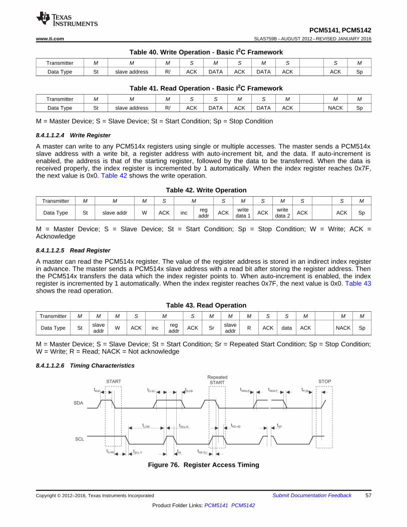
tBUF
tS-HD
tLOW
tD-SU tD-HD
tSCL-F
tSCL-R tRS-HD
tRS-SU
tSP
tP-SU
SDA
SCL
tHI
STARTRepeated
START STOP
tSDA-R tSDA-F
PCM5141, PCM5142www.ti.com SLAS759B –AUGUST 2012–REVISED JANUARY 2016
Table 40. Write Operation - Basic I2C FrameworkTransmitter M M M S M S M S S MData Type St slave address R/ ACK DATA ACK DATA ACK ACK Sp
Table 41. Read Operation - Basic I2C FrameworkTransmitter M M M S S M S M M MData Type St slave address R/ ACK DATA ACK DATA ACK NACK Sp
M = Master Device; S = Slave Device; St = Start Condition; Sp = Stop Condition
8.4.1.1.2.4 Write Register
A master can write to any PCM514x registers using single or multiple accesses. The master sends a PCM514xslave address with a write bit, a register address with auto-increment bit, and the data. If auto-increment isenabled, the address is that of the starting register, followed by the data to be transferred. When the data isreceived properly, the index register is incremented by 1 automatically. When the index register reaches 0x7F,the next value is 0x0. Table 42 shows the write operation.
Table 42. Write OperationTransmitter M M M S M S M S M S S M
reg write writeData Type St slave addr W ACK inc ACK ACK ACK ACK Spaddr data 1 data 2
M = Master Device; S = Slave Device; St = Start Condition; Sp = Stop Condition; W = Write; ACK =Acknowledge
8.4.1.1.2.5 Read Register
A master can read the PCM514x register. The value of the register address is stored in an indirect index registerin advance. The master sends a PCM514x slave address with a read bit after storing the register address. Thenthe PCM514x transfers the data which the index register points to. When auto-increment is enabled, the indexregister is incremented by 1 automatically. When the index register reaches 0x7F, the next value is 0x0. Table 43shows the read operation.
Table 43. Read OperationTransmitter M M M S M S M M M S S M M M
slave reg slaveData Type St W ACK inc ACK Sr R ACK data ACK NACK Spaddr addr addr
M = Master Device; S = Slave Device; St = Start Condition; Sr = Repeated Start Condition; Sp = Stop Condition;W = Write; R = Read; NACK = Not acknowledge
8.4.1.1.2.6 Timing Characteristics
Figure 76. Register Access Timing
Copyright © 2012–2016, Texas Instruments Incorporated Submit Documentation Feedback 57
Product Folder Links: PCM5141 PCM5142

PCM5141, PCM5142SLAS759B –AUGUST 2012–REVISED JANUARY 2016 www.ti.com
Table 44. I2C Bus TimingMIN MAX UNIT
Standard 100 kHzfSCL SCL clock frequency
Fast 400 kHzStandard 4.7
tBUF Bus free time between a STOP and START condition µsFast 1.3
Standard 4.7tLOW Low period of the SCL clock µs
Fast 1.3Standard 4.0 µs
tHI High period of the SCL clockFast 600 ns
Standard 4.7 µstRS-SU Setup time for (repeated)START condition
Fast 600 nstS-HD Standard 4.0 µs
Hold time for (repeated)START conditiontRS-HD Fast 600 ns
Standard 250tD-SU Data setup time ns
Fast 100Standard 0 900
tD-HD Data hold time nsFast 0 900
Standard 20 + 0.1CB 1000tSCL-R Rise time of SCL signal ns
Fast 20 + 0.1CB 300Standard 20 + 0.1CB 1000Rise time of SCL signal after a repeated STARTtSCL-R1 nscondition and after an acknowledge bit Fast 20 + 0.1CB 300Standard 20 + 0.1CB 1000
tSCL-F Fall time of SCL signal nsFast 20 + 0.1CB 300
Standard 20 + 0.1CB 1000tSDA-R Rise time of SDA signal ns
Fast 20 + 0.1CB 300Standard 20 + 0.1CB 1000
tSDA-F Fall time of SDA signal nsFast 20 + 0.1CB 300
Standard 4.0 µstP-SU Setup time for STOP condition
Fast 600 nsCB Capacitive load for SDA and SCL line 400 pFtSP Pulse width of spike suppressed Fast 50 nsVNH Noise margin at High level for each connected device (including hysteresis) 0.2 × VDD V
8.4.2 VREF and VCOM ModesSee Choosing Between VREF and VCOM Modes for information on configuring these modes.
8.5 ProgrammingIn software mode, the PCM514x can act as an I2S master, generating BCK and LRCK as outputs from the SCKinput.
Table 45. I2S Master Mode RegistersREGISTER FUNCTIONPage0, Register 9, D(0), D(4), and D(5) I2S Master mode selectRegister 32, D(6:0)
BCK divider and LRCK dividerRegister 33, D(7:0)
58 Submit Documentation Feedback Copyright © 2012–2016, Texas Instruments Incorporated
Product Folder Links: PCM5141 PCM5142

PCM514x
DNP
+
+
+
+
10 F 16Vm
+
3.3V
3.3VA
3.3VA
AGND
AGND
AGND
AGND
Right Channel Line Output
Left Channel Line Output
3.3V
PC
MA
udio
Sourc
eI
C Inte
rface
2
0.1 F
100V
m
10 F
16V
m
0.1 F
100V
m DNP
10 F
16V
m
DNP
10 F
16V
m0.1 F
100V
m
0.1 F
100V
m
2.2mF
25V
2.2mF
25V
DNP
10 F
16V
m
470W
470W
2.2nF 50V
2.2nF 50V
PCM5141, PCM5142www.ti.com SLAS759B –AUGUST 2012–REVISED JANUARY 2016
9 Application and Implementation
NOTEInformation in the following applications sections is not part of the TI componentspecification, and TI does not warrant its accuracy or completeness. TI’s customers areresponsible for determining suitability of components for their purposes. Customers shouldvalidate and test their design implementation to confirm system functionality.
9.1 Application InformationThe PCM514x family is flexible, and this flexibility gives rise to a number of design questions that define thedesign requirements for a given application.
9.2 Typical Application
Figure 77. Simplified Schematic, Hardware-Controlled Subsystem
9.2.1 Design Requirements• Single-ended 2.1-VRMS analog outputs• 3-wire I2S interface (BCK PLL)• Single 3.3-V supply
9.2.2 Detailed Design Procedure• Clock and PLL setup (See Reset and System Clock Functions.) Ensure incoming BCK meets minimum
requirements.• XSMT pin setup for 12-V monitoring (See External Power Sense Undervoltage Protection Mode.)• Single-supply 3.3-V operation (See Setting Digital Power Supplies and I/O Voltage Rails.)
Copyright © 2012–2016, Texas Instruments Incorporated Submit Documentation Feedback 59
Product Folder Links: PCM5141 PCM5142

-160
-140
-120
-100
-80
-60
-40
-20
0 5 10 15 20
Frequency (kHz)
Am
plit
ud
e (
dB
)
PCM5141, PCM5142SLAS759B –AUGUST 2012–REVISED JANUARY 2016 www.ti.com
Typical Application (continued)9.2.3 Application Curve
Figure 78. PCM5141A FFT Plot, DC to 20 kHz With a 1-kHz, –60-dBFS Input
60 Submit Documentation Feedback Copyright © 2012–2016, Texas Instruments Incorporated
Product Folder Links: PCM5141 PCM5142

PCM186x
DAC
Reference
PLL
Oscillator
AVDD 3.3V CPVDD 3.3V
Digital IODigital Core
(^W[, Logic etc)
DVDD (1.8V or 3.3v)
1.8V LDO Clock Halt Detect
LDOO 1.8V
Analog Circuits
Digital Circuits
Power CircuitsLine Driver
Charge Pump
PCM5141, PCM5142www.ti.com SLAS759B –AUGUST 2012–REVISED JANUARY 2016
10 Power Supply Recommendations
10.1 Power Supply Distribution and RequirementsThe PCM514x devices are powered through the pins shown in Figure 79.
Figure 79. Power Distribution Tree Within PCM514x
Table 46. Power Supply Pin DescriptionsNAME USAGE / DESCRIPTIONAVDD Analog voltage supply; must be 3.3 V. This powers all analog circuitry that the DAC runs on.DVDD Digital voltage supply. This is used as the I/O voltage control and the input to the onchip LDO.
CPVDD Charge Pump Voltage Supply - must be 3.3 VOutput from the onchip LDO. Should be used with a 0.1-µF decoupling cap. Can be driven (used as powerLDOO input) with a 1.8-V supply to bypass the onchip LDO for lower power consumption.
AGND Analog groundDGND Digital ground
10.2 Recommended Powerdown SequenceUnder certain conditions, the PCM514x devices can exhibit some pops on power down. Pops are caused by adevice not having enough time to detect power loss and start the muting process.
The PCM514x devices have two auto-mute functions to mute the device upon power loss (intentional orunintentional).
10.2.1 XSMT = 0When the XSMT pin is pulled low, the incoming PCM data is attenuated to 0, closely followed by a hard analogmute. This process takes 150 sample times (ts) + 0.2 ms.
Because this mute time is mainly dominated by the sampling frequency, systems sampling at 192 kHz will mutemuch faster than a 48-kHz system.
10.2.2 Clock Error DetectWhen clock error is detected on the incoming data clock, the PCM514x devices switch to an internal oscillator,and continue to the drive the output, while attenuating the data from the last known value. Once this process iscomplete, the PCM514x outputs are hard muted to ground.
Copyright © 2012–2016, Texas Instruments Incorporated Submit Documentation Feedback 61
Product Folder Links: PCM5141 PCM5142

3.3V
XSMT
I2S Clocks
SCK, BCK, LRCK
3 ms
VDD
0V
High
Low
High
Low
Time
3.3V
XSMT
I2S Clocks
SCK, BCK, LRCK
150t + 0.2msS
VDD
0V
High
Low
High
Low
Time
PCM5141, PCM5142SLAS759B –AUGUST 2012–REVISED JANUARY 2016 www.ti.com
Recommended Powerdown Sequence (continued)10.2.3 Planned ShutdownThese auto-muting processes can be manipulated by system designs to mute before power loss in the followingways:1. Assert XSMT low 150 tS + 0.2 ms before power is removed.
Figure 80. Assert XSMT
2. Stop I2S clocks (SCK, BCK, LRCK) 3 ms before powerdown as shown in Figure 81.
Figure 81. Stop I2C Clocks
10.2.4 Unplanned ShutdownMany systems use a low-noise regulator to provide an AVDD 3.3-V supply for the DAC. The XSMT Pin can takeadvantage of such a feature to measure the pre-regulated output from the system SMPS to mute the outputbefore the entire SMPS discharges. Figure 82 shows how to configure such a system to use the XSMT pin. TheXSMT pin can also be used in parallel with a GPIO pin from the system microcontroller/DSP or power supply.
62 Submit Documentation Feedback Copyright © 2012–2016, Texas Instruments Incorporated
Product Folder Links: PCM5141 PCM5142

PCM5xxx
Audio DAC
Linear
Regulator3.3V
10 F
GND GND
SMPS 6V
GNDXSMT
110V / 220V
MCU GPIO “mute” signal
PCM5141, PCM5142www.ti.com SLAS759B –AUGUST 2012–REVISED JANUARY 2016
Recommended Powerdown Sequence (continued)
Figure 82. Using the XSMT Pin
10.3 External Power Sense Undervoltage Protection Mode
NOTEExternal Power Sense Undervoltage Protection Mode is supported only whenDVDD = 3.3 V.
The XSMT pin can also be used to monitor a system voltage, such as the 24-VDC LCD TV backlight, or 12-VDCsystem supply using a voltage divider created with two resistors. (See Figure 83.)• If the XSMT pin makes a transition from 1 to 0 over 6 ms or more, the device switches into external
undervoltage protection mode. This mode uses two trigger levels:– When the XSMT pin level reaches 2 V, soft mute process begins.– When the XSMT pin level reaches 1.2 V, analog mute engages, regardless of digital audio level, and
analog shutdown begins. (DAC and related circuitry powers down).
If XSMT is moved from 1 to 0 in 20 ns or less, then the device will interpret it as a digital controlled request tomute. It will perform a soft mute, then move to standby.
A timing diagram to show this is shown in Figure 84.
NOTEThe XSMT input pin voltage range is from –0.3 V to DVDD + 0.3 V. The ratio of externalresistors must produce a voltage within this input range. Any increase in power supply(such as power supply positive noise or ripple) can pull the XSMT pin higher than DVDD +0.3 V.
For example, if the PCM514x is monitoring a 12-V input, and dividing the voltage by 4, then the voltage at XSMTduring ideal power supply conditions is 3.3 V. A voltage spike higher than 14.4 V causes a voltage greater than3.6 V (DVDD + 0.3) on the XSMT pin, potentially damaging the device.
Providing the divider is set appropriately, any DC voltage can be monitored.
Copyright © 2012–2016, Texas Instruments Incorporated Submit Documentation Feedback 63
Product Folder Links: PCM5141 PCM5142

System
VDD
XSMT
7.25kW
2.75kW
12V
supply
PCM5141, PCM5142SLAS759B –AUGUST 2012–REVISED JANUARY 2016 www.ti.com
External Power Sense Undervoltage Protection Mode (continued)
Figure 83. XSMT in External UVP Mode
Figure 84. XSMT Timing for Undervoltage Protection
The trigger voltage values for the soft mute and hard mute are shown in Table 47. The range of values will varyfrom device to device, but typical thresholds are shown. XSMT should be set up to nominally be 3.3 V along withDVDD, but derived from a higher system power supply rail.
Table 47. Distribution of Voltage ThresholdsMIN TYP MAX UNIT
Soft Mute Threshold Voltage 2 2.2 0.9 × DVDD VHard Mute Threshold Voltage 0.1 × DVDD 0.9 1.2 V
64 Submit Documentation Feedback Copyright © 2012–2016, Texas Instruments Incorporated
Product Folder Links: PCM5141 PCM5142
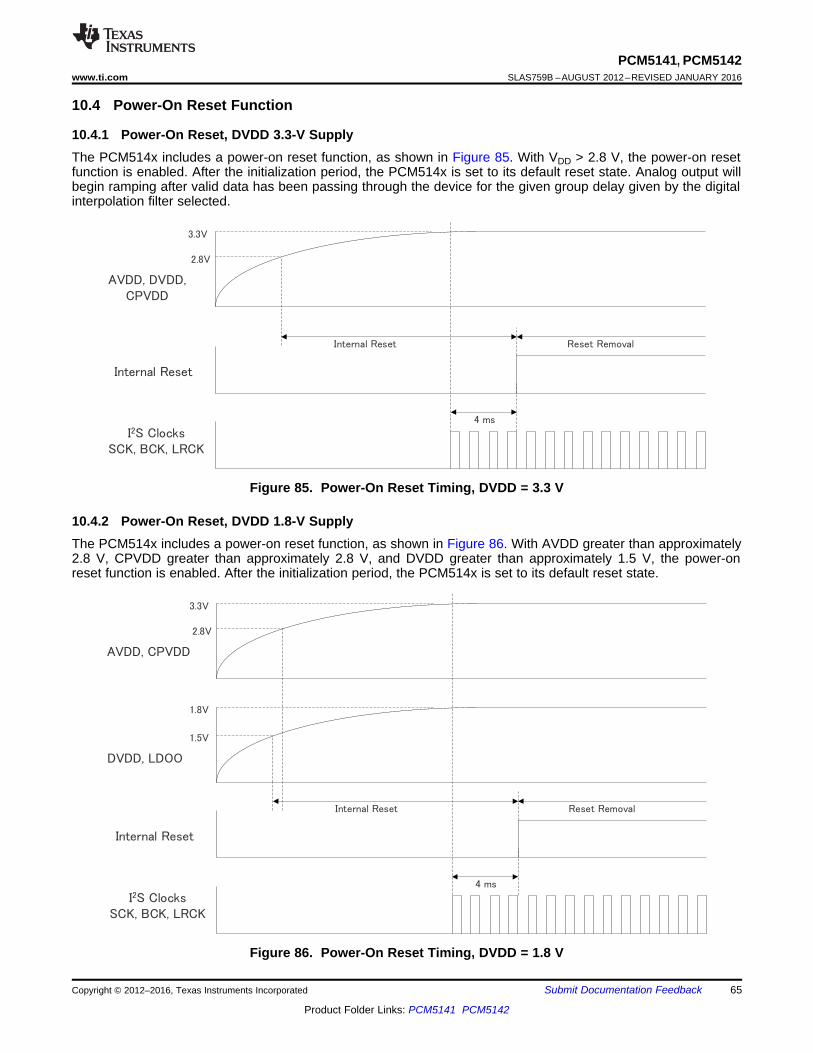
Internal Reset
I2S ClocksSCK, BCK, LRCK
Internal Reset
4 ms
Reset Removal
1.5V
1.8V
DVDD, LDOO
2.8V
3.3V
AVDD, CPVDD
Internal Reset
I2S ClocksSCK, BCK, LRCK
Internal Reset
4 ms
Reset Removal
2.8V
3.3V
AVDD, DVDD, CPVDD
PCM5141, PCM5142www.ti.com SLAS759B –AUGUST 2012–REVISED JANUARY 2016
10.4 Power-On Reset Function
10.4.1 Power-On Reset, DVDD 3.3-V SupplyThe PCM514x includes a power-on reset function, as shown in Figure 85. With VDD > 2.8 V, the power-on resetfunction is enabled. After the initialization period, the PCM514x is set to its default reset state. Analog output willbegin ramping after valid data has been passing through the device for the given group delay given by the digitalinterpolation filter selected.
Figure 85. Power-On Reset Timing, DVDD = 3.3 V
10.4.2 Power-On Reset, DVDD 1.8-V SupplyThe PCM514x includes a power-on reset function, as shown in Figure 86. With AVDD greater than approximately2.8 V, CPVDD greater than approximately 2.8 V, and DVDD greater than approximately 1.5 V, the power-onreset function is enabled. After the initialization period, the PCM514x is set to its default reset state.
Figure 86. Power-On Reset Timing, DVDD = 1.8 V
Copyright © 2012–2016, Texas Instruments Incorporated Submit Documentation Feedback 65
Product Folder Links: PCM5141 PCM5142

PCM5141, PCM5142SLAS759B –AUGUST 2012–REVISED JANUARY 2016 www.ti.com
10.5 PCM514x Power Modes
10.5.1 Setting Digital Power Supplies and I/O Voltage RailsThe internal digital core of the PCM514x devices run from a 1.8-V supply. This can be generated by the internalLDO, or by an external 1.8-V supply.
DVDD is used to set the I/O voltage, and to be used as the input to the onchip LDO that creates the 1.8 Vrequired by the digital core.
For systems that require 3.3-V I/O support, but lower power consumption, DVDD should be connected to 3.3 Vand LDOO can be connected to an external 1.8-V source. Doing so will disable the onchip LDO.
When setting I/O voltage to be 1.8 V, both DVDD and LDOO must be provided with an external 1.8-V supply.
10.5.2 Power Save ModesThe PCM514x devices offer two power-save modes: standby and power-down.
When a clock error (SCK, BCK, and LRCK) or clock halt is detected, the PCM514x device automatically entersstandby mode. The DAC and line driver are also powered down.
When BCK and LRCK remain at a low level for more than 1 second, the PCM514x device automatically enterspowerdown mode. Power-down mode disables the negative charge pump and bias/reference circuit, in additionto those disabled in standby mode.
When expected audio clocks (SCK, BCK, LRCK) are applied to the PCM514x device, or if BCK and LRCK startcorrectly while SCK remains at ground level for 16 successive LRCK periods, the device starts its powerupsequence automatically.
10.5.3 Power Save Parameter Programming
Table 48. Power Save RegistersREGISTER DESCRIPTION
Page 0, Register 2, D(4) Software standby mode commandPage 0, Register 2, D(0) Software power-down command
Software power-up sequence command (required after software standby or power-Page 0, Register 2, D(4) and D(0) down)Page 0, Register 44, D(2:0) Detection time of BCK and LRCK halt
66 Submit Documentation Feedback Copyright © 2012–2016, Texas Instruments Incorporated
Product Folder Links: PCM5141 PCM5142

1
Top Layer Ground Pour
Top Layer Signal Traces
Via to bottom Ground Plane
Pad to top layer ground pour
L-Ch Out
Rch Out
Make sure to have
ground pour separating
the Left and Right
channel traces to help
prevent crosstalk
2
3
4
5
6
7
8
9
10
11
12
13
14
28
27
26
25
24
23
22
21
20
19
18
17
16
15
CPVDD
CAPP
CPGND
CAPM
VNEG
OUTL
OUTR
AVDD
AGND
VCOM
SDA / MOSI
SCL / MC
GPIO5
GPIO4
DVDD
DGND
LDOO
XSMT
ADR1 /MISO
LRCK
DIN
BCK
SCK
GPIO6
MODE2 /MS
MODE1
ADR2
GPIO3
3.3V
0.1uF
0.1uF
Clock signals
from DSP or
Audio Processor
3.3V
Control Signals
from
Microcontroller
Control Signals
from
Microcontroller
Control Signals
from
Microcontroller
Capacitor values unless noted should be 2.2uF COG Ceramics
10uF
10uF
PCM5141, PCM5142www.ti.com SLAS759B –AUGUST 2012–REVISED JANUARY 2016
11 Layout
11.1 Layout Guidelines• The PCM514x family of devices are simple to layout. Most engineers use a shared common ground for an
entire device. GND can consider AGND and DGND connected.• Good system partitioning should keep digital clock and interface traces away from the analog outputs for
highest analog performance. This reduces any high-speed clock return currents influencing the analogoutputs.
• Power supply and charge pump decoupling capacitors should be placed as close as possible to the device.• The top layer should be used for routing signals, whilst the bottom layer can be used for GND.
11.2 Layout Example
It is recommended to place a top layer ground pour for shielding around the DAC and connect to lower main PCBground plane by multiple vias
Figure 87. PCM514x Layout Example
Copyright © 2012–2016, Texas Instruments Incorporated Submit Documentation Feedback 67
Product Folder Links: PCM5141 PCM5142

PCM5141, PCM5142SLAS759B –AUGUST 2012–REVISED JANUARY 2016 www.ti.com
12 Register Maps
12.1 PCM514x Register MapIn any page, register 0 is the Page Select Register. The register value selects the Register Page from 0 to 255for next read or write command.
Table 49. Register Map Overview (continued)Table 49. Register Map Overview REGISTER DESCRIPTIONNUMBERREGISTER DESCRIPTIONNUMBER 60 - 64 Digital volume
Page 0 65 Auto mute0 Page select register 75 - 79 Reserved1 Analog control register 80 - 85 GPIOn output selection2 Standby, Powerdown requests 86, 87 GPIO control3 Mute 88, 89 Reserved4 PLL Lock Flag, PLL enable 90 DSP overflow5 Reserved 91 - 94 Sample rate status6 SPI MISO function select 95 - 107 Reserved7 De-emphasis enable, SDOUT select 108 Analog mute monitor8 GPIO enables 109 - 118 Reserved9 BCK, LRCLK configuration 119 GPIO input10 DSP GPIO Input 120 Auto Mute flags11 Reserved 121 Reserved12 Master mode BCK, LRCLK reset Page 113 PLL clock source select 1 Output amplitude type14 - 19 Reserved 2 Analog gain control20 - 24 PLL dividers 3, 4 Reserved25, 26 Reserved 5 Undervoltage protection27 DSP clock divider 6 Analog mute control28 DAC clock divider 7 Analog gain boost29 NCP clock divider 8, 9 VCOM configuration30 OSR clock divider Page 4431 Reserved 1 Coefficient memory (CRAM) control32, 33 Master mode dividers Pages 44 - 52 Coefficient buffer - A (256 coeffs x 24 bits) : See
Table 5134 fS speed modePages 62 - 70 Coefficient buffer - B (256 coeffs x 24 bits) : See35, 36 IDAC (number of DSP clock cycles available in
Table 52one audio frame)Pages 152 - Instruction buffer (1024 instruction x 25 bits),37 Ignore various errors186 I512 - I1023 are reserved.: See Table 53
38,39 ReservedPages 187 - Reserved
40, 41 I2S configuration 25242 DAC data path Page 25343 DSP program selection 63, 64 Clock Flex Mode44 Clock missing detection period Pages 254 - Reserved
25559 Auto mute time
68 Submit Documentation Feedback Copyright © 2012–2016, Texas Instruments Incorporated
Product Folder Links: PCM5141 PCM5142

PCM5141, PCM5142www.ti.com SLAS759B –AUGUST 2012–REVISED JANUARY 2016
The PCM514x has a register map split into multiple pages. Pages 0 and 1 control of the DAC and other on-chipperipherals. Pages 44 through 52 are used for Coefficient A memory, while Pages 62-70 are coefficient Bmemory. Pages 152-186 contain the miniDSP instruction memory. Page 253 is where the Clock Flex Moderegister is located.
Table 50. PCM514x Register Page StructurePage: 0 1 44-52 62-70 152-186 253
2-43
53-6
1
71-1
51
187-
252
254-
255
Func: Control Analog Coeffient A Coeffient B InstructionControl
Clo
ckFl
ex
Desc: General Analog 256 24-bit coefficients, 256 24-bit coefficients, 1024 24-bit instructions,Control and Control 30 coefficients per 30 coefficients per 30 instructions perConfiguration page, page, page,R
eser
ved
Res
erve
d
Res
erve
d
Res
erve
d
Res
erve
d
4 registers per 4 registers per 4 registers percoefficient coefficient instruction
Clo
ckFl
exM
ode
Table 51. Coefficient Buffer-A MapCOEFF NO PAGE NO BASE REGISTER BASE REGISTER + 0 BASE REGISTER + 1 BASE REGISTER + 2 BASE REGISTER + 3
C0 44 8 Coef(23:16) Coef(15:8) Coef(7:0) Reserved.
C1 44 12 Coef(23:16) Coef(15:8) Coef(7:0) Reserved.
.. .. .. .. .. .. ..
C29 44 124 Coef(23:16) Coef(15:8) Coef(7:0) Reserved.
C30 45 8 Coef(23:16) Coef(15:8) Coef(7:0) Reserved.
.. .. .. .. .. .. ..
C59 45 124 Coef(23:16) Coef(15:8) Coef(7:0) Reserved.
C60 46 8 Coef(23:16) Coef(15:8) Coef(7:0) Reserved.
.. .. .. .. .. .. ..
C89 46 124 Coef(23:16) Coef(15:8) Coef(7:0) Reserved.
C90 47 8 Coef(23:16) Coef(15:8) Coef(7:0) Reserved.
.. .. .. .. .. .. ..
C119 47 124 Coef(23:16) Coef(15:8) Coef(7:0) Reserved.
C120 48 8 Coef(23:16) Coef(15:8) Coef(7:0) Reserved.
.. .. .. .. .. .. ..
C149 48 124 Coef(23:16) Coef(15:8) Coef(7:0) Reserved.
C150 49 8 Coef(23:16) Coef(15:8) Coef(7:0) Reserved.
.. .. .. .. .. .. ..
C179 49 124 Coef(23:16) Coef(15:8) Coef(7:0) Reserved.
C180 50 8 Coef(23:16) Coef(15:8) Coef(7:0) Reserved.
.. .. .. .. .. .. ..
C209 50 124 Coef(23:16) Coef(15:8) Coef(7:0) Reserved.
C210 51 8 Coef(23:16) Coef(15:8) Coef(7:0) Reserved.
.. .. .. .. .. .. ..
C239 51 124 Coef(23:16) Coef(15:8) Coef(7:0) Reserved.
C240 52 8 Coef(23:16) Coef(15:8) Coef(7:0) Reserved.
.. .. .. .. .. .. ..
C255 52 68 Coef(23:16) Coef(15:8) Coef(7:0) Reserved.
Copyright © 2012–2016, Texas Instruments Incorporated Submit Documentation Feedback 69
Product Folder Links: PCM5141 PCM5142

PCM5141, PCM5142SLAS759B –AUGUST 2012–REVISED JANUARY 2016 www.ti.com
Table 52. Coefficient Buffer-B MapCOEFF NO PAGE NO BASE REGISTER BASE REGISTER + 0 BASE REGISTER + 1 BASE REGISTER + 2 BASE REGISTER + 3
C0 62 8 Coef(23:16) Coef(15:8) Coef(7:0) Reserved.
C1 62 12 Coef(23:16) Coef(15:8) Coef(7:0) Reserved.
.. .. .. .. .. .. ..
C29 62 124 Coef(23:16) Coef(15:8) Coef(7:0) Reserved.
C30 63 8 Coef(23:16) Coef(15:8) Coef(7:0) Reserved.
.. .. .. .. .. .. ..
C59 63 124 Coef(23:16) Coef(15:8) Coef(7:0) Reserved.
C60 64 8 Coef(23:16) Coef(15:8) Coef(7:0) Reserved.
.. .. .. .. .. .. ..
C89 64 124 Coef(23:16) Coef(15:8) Coef(7:0) Reserved.
C90 65 8 Coef(23:16) Coef(15:8) Coef(7:0) Reserved.
.. .. .. .. .. .. ..
C119 65 124 Coef(23:16) Coef(15:8) Coef(7:0) Reserved.
C120 66 8 Coef(23:16) Coef(15:8) Coef(7:0) Reserved.
.. .. .. .. .. .. ..
C149 66 124 Coef(23:16) Coef(15:8) Coef(7:0) Reserved.
C150 67 8 Coef(23:16) Coef(15:8) Coef(7:0) Reserved.
.. .. .. .. .. .. ..
C179 67 124 Coef(23:16) Coef(15:8) Coef(7:0) Reserved.
C180 68 8 Coef(23:16) Coef(15:8) Coef(7:0) Reserved.
.. .. .. .. .. .. ..
C209 68 124 Coef(23:16) Coef(15:8) Coef(7:0) Reserved.
C210 69 8 Coef(23:16) Coef(15:8) Coef(7:0) Reserved.
.. .. .. .. .. .. ..
C239 69 124 Coef(23:16) Coef(15:8) Coef(7:0) Reserved.
C240 70 8 Coef(23:16) Coef(15:8) Coef(7:0) Reserved.
.. .. .. .. .. .. ..
C255 70 68 Coef(23:16) Coef(15:8) Coef(7:0) Reserved.
Table 53. miniDSP Instruction MapCOEFF NO PAGE NO BASE REGISTER BASE REGISTER + 0 BASE REGISTER + 1 BASE REGISTER + 2 BASE REGISTER + 3
I0 152 8 Instr(31:24) Instr(23:16) Instr(15:8) Instr(7:0)
I1 152 12 Instr(31:24) Instr(23:16) Instr(15:8) Instr(7:0)
.. .. .. .. .. .. ..
I29 152 124 Instr(31:24) Instr(23:16) Instr(15:8) Instr(7:0)
I30 153 8 Instr(31:24) Instr(23:16) Instr(15:8) Instr(7:0)
.. .. .. .. .. .. ..
I59 153 124 Instr(31:24) Instr(23:16) Instr(15:8) Instr(7:0)
I60 154 8 Instr(31:24) Instr(23:16) Instr(15:8) Instr(7:0)
.. .. .. .. .. .. ..
I89 154 124 Instr(31:24) Instr(23:16) Instr(15:8) Instr(7:0)
I90 155 8 Instr(31:24) Instr(23:16) Instr(15:8) Instr(7:0)
.. .. .. .. .. .. ..
I119 155 124 Instr(31:24) Instr(23:16) Instr(15:8) Instr(7:0)
I120 156 8 Instr(31:24) Instr(23:16) Instr(15:8) Instr(7:0)
.. .. .. .. .. .. ..
I149 156 124 Instr(31:24) Instr(23:16) Instr(15:8) Instr(7:0)
I150 157 8 Instr(31:24) Instr(23:16) Instr(15:8) Instr(7:0)
.. .. .. .. .. .. ..
I179 157 124 Instr(31:24) Instr(23:16) Instr(15:8) Instr(7:0)
I180 158 8 Instr(31:24) Instr(23:16) Instr(15:8) Instr(7:0)
.. .. .. .. .. .. ..
I209 158 124 Instr(31:24) Instr(23:16) Instr(15:8) Instr(7:0)
I210 159 8 Instr(31:24) Instr(23:16) Instr(15:8) Instr(7:0)
.. .. .. .. .. .. ..
70 Submit Documentation Feedback Copyright © 2012–2016, Texas Instruments Incorporated
Product Folder Links: PCM5141 PCM5142

PCM5141, PCM5142www.ti.com SLAS759B –AUGUST 2012–REVISED JANUARY 2016
Table 53. miniDSP Instruction Map (continued)COEFF NO PAGE NO BASE REGISTER BASE REGISTER + 0 BASE REGISTER + 1 BASE REGISTER + 2 BASE REGISTER + 3
I239 159 124 Instr(31:24) Instr(23:16) Instr(15:8) Instr(7:0)
I240 160 8 Instr(31:24) Instr(23:16) Instr(15:8) Instr(7:0)
.. .. .. .. .. .. ..
I269 160 124 Instr(31:24) Instr(23:16) Instr(15:8) Instr(7:0)
I270 161 8 Instr(31:24) Instr(23:16) Instr(15:8) Instr(7:0)
.. .. .. .. .. .. ..
I299 161 124 Instr(31:24) Instr(23:16) Instr(15:8) Instr(7:0)
I300 162 8 Instr(31:24) Instr(23:16) Instr(15:8) Instr(7:0)
.. .. .. .. .. .. ..
I329 162 124 Instr(31:24) Instr(23:16) Instr(15:8) Instr(7:0)
I330 163 8 Instr(31:24) Instr(23:16) Instr(15:8) Instr(7:0)
.. .. .. .. .. .. ..
I359 163 124 Instr(31:24) Instr(23:16) Instr(15:8) Instr(7:0)
I360 164 8 Instr(31:24) Instr(23:16) Instr(15:8) Instr(7:0)
.. .. .. .. .. .. ..
I389 164 124 Instr(31:24) Instr(23:16) Instr(15:8) Instr(7:0)
I390 165 8 Instr(31:24) Instr(23:16) Instr(15:8) Instr(7:0)
.. .. .. .. .. .. ..
I419 165 124 Instr(31:24) Instr(23:16) Instr(15:8) Instr(7:0)
I420 166 8 Instr(31:24) Instr(23:16) Instr(15:8) Instr(7:0)
.. .. .. .. .. .. ..
I449 166 124 Instr(31:24) Instr(23:16) Instr(15:8) Instr(7:0)
I450 167 8 Instr(31:24) Instr(23:16) Instr(15:8) Instr(7:0)
.. .. .. .. .. .. ..
I479 167 124 Instr(31:24) Instr(23:16) Instr(15:8) Instr(7:0)
I480 168 8 Instr(31:24) Instr(23:16) Instr(15:8) Instr(7:0)
.. .. .. .. .. .. ..
I509 168 124 Instr(31:24) Instr(23:16) Instr(15:8) Instr(7:0)
I510 169 8 Instr(31:24) Instr(23:16) Instr(15:8) Instr(7:0)
I511 169 12 Instr(31:24) Instr(23:16) Instr(15:8) Instr(7:0)
.. .. .. .. .. .. ..
I539 169 124 Reserved. Reserved. Reserved. Reserved.
I540 170 8 Reserved. Reserved. Reserved. Reserved.
.. .. .. .. .. .. ..
I569 170 124 Reserved. Reserved. Reserved. Reserved.
I570 171 8 Reserved. Reserved. Reserved. Reserved.
.. .. .. .. .. .. ..
I599 171 124 Reserved. Reserved. Reserved. Reserved.
I600 172 8 Reserved. Reserved. Reserved. Reserved.
.. .. .. .. .. .. ..
I629 172 124 Reserved. Reserved. Reserved. Reserved.
I630 173 8 Reserved. Reserved. Reserved. Reserved.
.. .. .. .. .. .. ..
I659 173 124 Reserved. Reserved. Reserved. Reserved.
I660 174 8 Reserved. Reserved. Reserved. Reserved.
.. .. .. .. .. .. ..
I689 174 124 Reserved. Reserved. Reserved. Reserved.
I690 175 8 Reserved. Reserved. Reserved. Reserved.
.. .. .. .. .. .. ..
I719 175 124 Reserved. Reserved. Reserved. Reserved.
I720 176 8 Reserved. Reserved. Reserved. Reserved.
.. .. .. .. .. .. ..
I749 176 124 Reserved. Reserved. Reserved. Reserved.
I750 177 8 Reserved. Reserved. Reserved. Reserved.
.. .. .. .. .. .. ..
I779 177 124 Reserved. Reserved. Reserved. Reserved.
Copyright © 2012–2016, Texas Instruments Incorporated Submit Documentation Feedback 71
Product Folder Links: PCM5141 PCM5142

PCM5141, PCM5142SLAS759B –AUGUST 2012–REVISED JANUARY 2016 www.ti.com
Table 53. miniDSP Instruction Map (continued)COEFF NO PAGE NO BASE REGISTER BASE REGISTER + 0 BASE REGISTER + 1 BASE REGISTER + 2 BASE REGISTER + 3
I780 178 8 Reserved. Reserved. Reserved. Reserved.
.. .. .. .. .. .. ..
I809 178 124 Reserved. Reserved. Reserved. Reserved.
I810 179 8 Reserved. Reserved. Reserved. Reserved.
.. .. .. .. .. .. ..
I839 179 124 Reserved. Reserved. Reserved. Reserved.
I840 180 8 Reserved. Reserved. Reserved. Reserved.
.. .. .. .. .. .. ..
I869 180 124 Reserved. Reserved. Reserved. Reserved.
I870 181 8 Reserved. Reserved. Reserved. Reserved.
.. .. .. .. .. .. ..
I899 181 124 Reserved. Reserved. Reserved. Reserved.
I900 182 8 Reserved. Reserved. Reserved. Reserved.
.. .. .. .. .. .. ..
I929 182 124 Reserved. Reserved. Reserved. Reserved.
I930 183 8 Reserved. Reserved. Reserved. Reserved.
.. .. .. .. .. .. ..
I959 183 124 Reserved. Reserved. Reserved. Reserved.
I960 184 8 Reserved. Reserved. Reserved. Reserved.
.. .. .. .. .. .. ..
I989 184 124 Reserved. Reserved. Reserved. Reserved.
I990 185 8 Reserved. Reserved. Reserved. Reserved.
.. .. .. .. .. .. ..
I1019 185 124 Reserved. Reserved. Reserved. Reserved.
I1020 186 8 Reserved. Reserved. Reserved. Reserved.
.. .. .. .. .. .. ..
I1023 186 20 Reserved. Reserved. Reserved. Reserved.
72 Submit Documentation Feedback Copyright © 2012–2016, Texas Instruments Incorporated
Product Folder Links: PCM5141 PCM5142

PCM5141, PCM5142www.ti.com SLAS759B –AUGUST 2012–REVISED JANUARY 2016
12.1.1 Detailed Register Descriptions
12.1.1.1 Register Map Summary
Table 54. Register Map SummaryDEC HEX B7 B6 B5 B4 B3 B2 B1 B0
Page 01 01 RSV RSV RSV RSTM RSV RSV RSV RSTR2 02 RSV RSV RSV RQST RSV RSV RSV RQPD3 03 RSV RSV RSV RQML RSV RSV RSV RQMR4 04 RSV RSV RSV PLCK RSV RSV RSV PLLE6 06 RSV RSV RSV RSV RSV RSV FSMI1 FSMI07 07 RSV RSV RSV DEMP RSV RSV RSV SDSL8 08 RSV RSV G6OE G5OE G4OE G3OE G2OE G1OE9 09 RSV RSV BCKP BCKO RSV RSV RSV LRKO10 0A DSPG7 DSPG6 DSPG5 DSPG4 DSPG3 DSPG2 DSPG1 DSPG012 0C RSV RSV RSV RSV RSV RSV RBCK RLRK13 0D RSV SREF2 SREF1 SREF0 RSV RSV RSV RSV14 0E RSV SDAC2 SDAC1 SDAC0 RSV RSV RSV RSV18 12 RSV RSV RSV RSV RSV GREF2 GREF1 GREF019 13 RSV RSV RSV RSV RSV RSV RSV RQSY20 14 RSV RSV RSV RSV PPDV3 PPDV2 PPDV1 PPDV021 15 RSV RSV PJDV5 PJDV4 PJDV3 PJDV2 PJDV1 PJDV022 16 RSV RSV PDDV13 PDDV12 PDDV11 PDDV10 PDDV9 PDDV823 17 PDDV7 PDDV6 PDDV5 PDDV4 PDDV3 PDDV2 PDDV1 PDDV024 18 RSV RSV RSV RSV PRDV3 PRDV2 PRDV1 PRDV027 1B RSV DDSP6 DDSP5 DDSP4 DDSP3 DDSP2 DDSP1 DDSP028 1C RSV DDAC6 DDAC5 DDAC4 DDAC3 DDAC2 DDAC1 DDAC029 1D RSV DNCP6 DNCP5 DNCP4 DNCP3 DNCP2 DNCP1 DNCP030 1E RSV DOSR6 DOSR5 DOSR4 DOSR3 DOSR2 DOSR1 DOSR032 20 RSV DBCK6 DBCK5 DBCK4 DBCK3 DBCK2 DBCK1 DBCK033 21 DLRK7 DLRK6 DLRK5 DLRK4 DLRK3 DLRK2 DLRK1 DLRK034 22 RSV RSV RSV I16E RSV RSV FSSP1 FSSP035 23 IDAC15 IDAC14 IDAC13 IDAC12 IDAC11 IDAC10 IDAC9 IDAC836 24 IDAC7 IDAC6 IDAC5 IDAC4 IDAC3 IDAC2 IDAC1 IDAC037 25 RSV IDFS IDBK IDSK IDCH IDCM DCAS IPLK40 28 RSV RSV AFMT1 AFMT0 RSV RSV ALEN1 ALEN041 29 AOFS7 AOFS6 AOFS5 AOFS4 AOFS3 AOFS2 AOFS1 AOFS042 2A RSV RSV AUPL1 AUPL0 RSV RSV AUPR1 AUPR043 2B RSV RSV RSV PSEL4 PSEL3 PSEL2 PSEL1 PSEL044 2C RSV RSV RSV RSV RSV CMDP2 CMDP1 CMDP059 3B RSV AMTL2 AMTL1 AMTL0 RSV AMTR2 AMTR1 AMTR060 3C RSV RSV RSV RSV RSV RSV PCTL1 PCTL061 3D VOLL7 VOLL6 VOLL5 VOLL4 VOLL3 VOLL2 VOLL1 VOLL062 3E VOLR7 VOLR6 VOLR5 VOLR4 VOLR3 VOLR2 VOLR1 VOLR063 3F VNDF1 VNDF0 VNDS1 VNDS0 VNUF1 VNUF0 VNUS1 VNUS064 40 VEDF1 VEDF0 VEDS1 VEDS0 RSV RSV RSV RSV65 41 RSV RSV RSV RSV RSV ACTL2 AMLE1 AMRE080 50 RSV RSV RSV G1SL4 G1SL3 G1SL2 G1SL1 G1SL081 51 RSV RSV RSV G2SL4 G2SL3 G2SL2 G2SL1 G2SL0
Copyright © 2012–2016, Texas Instruments Incorporated Submit Documentation Feedback 73
Product Folder Links: PCM5141 PCM5142

PCM5141, PCM5142SLAS759B –AUGUST 2012–REVISED JANUARY 2016 www.ti.com
Table 54. Register Map Summary (continued)DEC HEX B7 B6 B5 B4 B3 B2 B1 B082 52 RSV RSV RSV G3SL4 G3SL3 G3SL2 G3SL1 G3SL083 53 RSV RSV RSV G4SL4 G4SL3 G4SL2 G4SL1 G4SL084 54 RSV RSV RSV G5SL4 G5SL3 G5SL2 G5SL1 G5SL085 55 RSV RSV RSV G6SL4 G6SL3 G6SL2 G6SL1 G6SL086 56 RSV RSV GOUT5 GOUT4 GOUT3 GOUT2 GOUT1 GOUT087 57 RSV RSV GINV5 GINV4 GINV3 GINV2 GINV1 GINV090 5A RSV RSV RSV L1OV R1OV L2OV R2OV SFOV91 5B RSV DTFS2 DTFS1 DTFS0 DTSR3 DTSR2 DTSR1 DTSR092 5C RSV RSV RSV RSV RSV RSV RSV DTBR893 5D DTBR7 DTBR6 DTBR5 DTBR4 DTBR3 DTBR2 DTBR1 DTBR094 5E RSV CDST PLL-L LrckBck fS-SCKr SCKval BCKval fSval95 5F RSV RSV RSV LTSH RSV CKMF CSRF CERF108 6C RSV RSV RSV RSV RSV RSV AMLM AMRM109 6D RSV RSV RSV SDTM RSV RSV RSV SHTM114 72 RSV RSV RSV RSV RSV RSV MTST1 MTST0115 73 RSV RSV RSV RSV RSV RSV FSMM1 FSMM0118 76 BOTM RSV RSV RSV PSTM3 PSTM2 PSTM1 PSTM0119 77 RSV RSV GPIN5 GPIN4 GPIN3 GPIN2 GPIN1 RSV120 78 RSV RSV RSV AMFL RSV RSV RSV AMFR121 79 RSV RSV RSV RSV RSV RSV RSV DAMD122 7A RSV RSV RSV RSV RSV RSV RSV EIFM123 7B RSV G1MC2 G1MC1 G1MC0 RSV G2MC2 G2MC1 G2MC0124 7C RSV G3MC2 G3MC1 G3MC0 RSV G4MC2 G4MC1 G4MC0125 7D RSV G5MC2 G5MC1 G5MC0 RSV G6MC2 G6MC1 G6MC0
Page 1Dec Hex b7 b6 b5 b4 b3 b2 b1 b0
1 01 RSV RSV RSV RSV RSV RSV RSV OSEL2 02 RSV RSV RSV LAGN RSV RSV RSV RAGN5 05 RSV RSV RSV RSV RSV RSV UEPD UIPD6 06 RSV RSV RSV RSV RSV RSV RSV AMCT7 07 RSV RSV RSV AGBL RSV RSV RSV AGBR8 08 RSV RSV RSV RSV RSV RSV RSV RCMF9 09 RSV RSV RSV RSV RSV RSV RSV VCPD
Page 44Dec Hex b7 b6 b5 b4 b3 b2 b1 b0
1 01 RSV RSV RSV RSV ACRM AMDC ACRS ACSWPage 253
Dec Hex b7 b6 b5 b4 b3 b2 b1 b063 3F PLLFLEX17 PLLFLEX16 PLLFLEX15 PLLFLEX14 PLLFLEX13 PLLFLEX12 PLLFLEX11 PLLFLEX1064 40 PLLFLEX27 PLLFLEX26 PLLFLEX25 PLLFLEX24 PLLFLEX23 PLLFLEX22 PLLFLEX21 PLLFLEX20
12.1.1.2 Page 0 Registers
Table 55. Page 0 / Register 1Dec Hex b7 b6 b5 b4 b3 b2 b1 b0
1 01 RSV RSV RSV RSTM RSV RSV RSV RSTRReset Value 0 0
74 Submit Documentation Feedback Copyright © 2012–2016, Texas Instruments Incorporated
Product Folder Links: PCM5141 PCM5142

PCM5141, PCM5142www.ti.com SLAS759B –AUGUST 2012–REVISED JANUARY 2016
RSV ReservedReserved. Do not access.
RSTM Reset ModulesThis bit resets the interpolation filter and the DAC modules. Since the DSP is also reset, the coeffient RAMcontent will also be cleared by the DSP. This bit is auto cleared and can be set only in standby mode.
Default value: 00: Normal1: Reset modules
RSTR Reset RegistersThis bit resets the mode registers back to their initial values. The RAM content is not cleared, but the executionsource will be back to ROM. This bit is auto cleared and must be set only when the DAC is in standby mode(resetting registers when the DAC is running is prohibited and not supported).
Default value: 00: Normal1: Reset mode registers
Table 56. Page 0 / Register 2Dec Hex b7 b6 b5 b4 b3 b2 b1 b0
2 02 RSV RSV RSV RQST RSV RSV RSV RQPDReset Value 0 0
RSV ReservedReserved. Do not access.
RQST Standby RequestWhen this bit is set, the DAC will be forced into a system standby mode, which is also the mode the systementers in the case of clock errors. In this mode, most subsystems will be powered down but the charge pumpand digital power supply.
Default value: 00: Normal operation1: Standby mode
RQPD Powerdown RequestWhen this bit is set, the DAC will be forced into powerdown mode, in which the power consumption would beminimum as the charge pump is also powered down. However, it will take longer to restart from this mode. Thismode has higher precedence than the standby mode, that is, setting this bit along with bit 4 for standby modewill result in the DAC going into powerdown mode.
Default value: 00: Normal operation1: Powerdown mode
Table 57. Page 0 / Register 3Dec Hex b7 b6 b5 b4 b3 b2 b1 b0
3 03 RSV RSV RSV RQML RSV RSV RSV RQMRReset Value 0 0
RSV ReservedReserved. Do not access.
RQML Mute Left ChannelThis bit issues soft mute request for the left channel. The volume will be smoothly ramped down/up to avoidpop/click noise.
Default value: 00: Normal volume1: Mute
Copyright © 2012–2016, Texas Instruments Incorporated Submit Documentation Feedback 75
Product Folder Links: PCM5141 PCM5142

PCM5141, PCM5142SLAS759B –AUGUST 2012–REVISED JANUARY 2016 www.ti.com
RQMR Mute Right ChannelThis bit issues soft mute request for the right channel. The volume will be smoothly ramped down/up to avoidpop/click noise.
Default value: 00: Normal volume1: Mute
Table 58. Page 0 / Register 4Dec Hex b7 b6 b5 b4 b3 b2 b1 b0
4 04 RSV RSV RSV PLCK RSV RSV RSV PLLEReset Value 1
RSV ReservedReserved. Do not access.
PLCK PLL Lock Flag (Read Only)This bit indicates whether the PLL is locked or not. When the PLL is disabled this bit always shows that thePLL is not locked.
0: The PLL is locked1: The PLL is not locked
PLLE PLL EnableThis bit enables or disables the internal PLL. When PLL is disabled, the master clock will be switched to theSCK.
Default value: 10: Disable PLL1: Enable PLL
Table 59. Page 0 / Register 6Dec Hex b7 b6 b5 b4 b3 b2 b1 b0
6 06 RSV RSV RSV RSV RSV RSV FSMI1 FSMI0Reset Value 0 0
RSV ReservedReserved. Do not access.
FSMI[1:0] SPI MISO function selThese bits select the function of the SPI_MISO pin when in SPI mode. If the pin is set as GPIO, registerreadout via SPI is not possible.
Default value: 0000: SPI_MISO01: GPIO1Others: Reserved (Do not set)
Table 60. Page 0 / Register 7Dec Hex b7 b6 b5 b4 b3 b2 b1 b0
7 07 RSV RSV RSV DEMP RSV RSV RSV SDSLReset Value 0 0
RSV ReservedReserved. Do not access.
DEMP De-Emphasis EnableThis bit enables or disables the de-emphasis filter. The default coefficients are for 44.1kHz sampling rate, butcan be changed by reprogramming the appropriate coeffients in RAM.
76 Submit Documentation Feedback Copyright © 2012–2016, Texas Instruments Incorporated
Product Folder Links: PCM5141 PCM5142

PCM5141, PCM5142www.ti.com SLAS759B –AUGUST 2012–REVISED JANUARY 2016
Default value: 00: De-emphasis filter is disabled1: De-emphasis filter is enabled
SDSL SDOUT SelectThis bit selects what is being output as SDOUT via GPIO pins.
Default value: 00: SDOUT is the DSP output (post-processing)1: SDOUT is the DSP input (pre-processing)
Table 61. Page 0 / Register 8Dec Hex b7 b6 b5 b4 b3 b2 b1 b0
8 08 RSV RSV G6OE G5OE G4OE G3OE G2OE G1OEReset Value 0 0 0 0 0 0
RSV ReservedReserved. Do not access.
G6OE GPIO6 Output EnableThis bit sets the direction of the GPIO6 pin
Default value: 00: GPIO6 is input1: GPIO6 is output
G5OE GPIO5 Output EnableThis bit sets the direction of the GPIO5 pin
Default value: 00: GPIO5 is input1: GPIO5 is output
G4OE GPIO4 Output EnableThis bit sets the direction of the GPIO4 pin
Default value: 00: GPIO4 is input1: GPIO4 is output
G3OE GPIO3 Output EnableThis bit sets the direction of the GPIO3 pin
Default value: 00: GPIO3 is input1: GPIO3 is output
G2OE GPIO2 Output EnableThis bit sets the direction of the GPIO2 pin
Default value: 00: GPIO2 is input1: GPIO2 is output
G1OE GPIO1 Output EnableThis bit sets the direction of the GPIO1 pin
Default value: 00: GPIO1 is input1: GPIO1 is output
Copyright © 2012–2016, Texas Instruments Incorporated Submit Documentation Feedback 77
Product Folder Links: PCM5141 PCM5142

PCM5141, PCM5142SLAS759B –AUGUST 2012–REVISED JANUARY 2016 www.ti.com
Table 62. Page 0 / Register 9Dec Hex b7 b6 b5 b4 b3 b2 b1 b0
9 09 RSV RSV BCKP BCKO RSV RSV RSV LRKOReset Value 0 0 0
RSV ReservedReserved. Do not access.
BCKP BCK PolarityThis bit sets the inverted BCK mode. In inverted BCK mode, the DAC assumes that the LRCK and DIN edgesare aligned to the rising edge of the BCK. Normally they are assumed to be aligned to the falling edge of theBCK.
Default value: 00: Normal BCK mode1: Inverted BCK mode
BCKO BCK Output EnableThis bit sets the BCK pin direction to output for I2S master mode operation. In I2S master mode the PCM5xxxoutputs the reference BCK and LRCK, and the external source device provides the DIN according to theseclocks. Use Page 0 / Register 32 to program the division factor of the SCK to yield the desired BCK rate(normally 64FS)
Default value: 00: BCK is input (I2S slave mode)1: BCK is output (I2S master mode)
LRKO LRCLK Output EnableThis bit sets the LRCK pin direction to output for I2S master mode operation. In I2S master mode the PCM5xxxoutputs the reference BCK and LRCK, and the external source device provides the DIN according to theseclocks. Use Page 0 / Register 33 to program the division factor of the BCK to yield 1FS for LRCK.
Default value: 00: LRCK is input (I2S slave mode)1: LRCK is output (I2S master mode)
Table 63. Page 0 / Register 10Dec Hex b7 b6 b5 b4 b3 b2 b1 b010 0A DSPG7 DSPG6 DSPG5 DSPG4 DSPG3 DSPG2 DSPG1 DSPG0
Reset Value 0 0 0 0 0 0 0 0
DSPG[7:0] DSP GPIO InputThe DSP accepts a 24-bit external control signals input. The value set in this register will go to bit 16:8 of thisexternal input.
Default value: 00000000
Table 64. Page 0 / Register 12Dec Hex b7 b6 b5 b4 b3 b2 b1 b012 0C RSV RSV RSV RSV RSV RSV RBCK RLRK
Reset Value 0 0
RSV ReservedReserved. Do not access.
RBCK Master Mode BCK Divider ResetThis bit, when set to 0, will reset the SCK divider to generate BCK clock for I2S master mode. To use I2Smaster mode, the divider must be enabled and programmed properly.
Default value: 00: Master mode BCK clock divider is reset
78 Submit Documentation Feedback Copyright © 2012–2016, Texas Instruments Incorporated
Product Folder Links: PCM5141 PCM5142

PCM5141, PCM5142www.ti.com SLAS759B –AUGUST 2012–REVISED JANUARY 2016
1: Master mode BCK clock divider is functionalRLRK Master Mode LRCK Divider Reset
This bit, when set to 0, will reset the BCK divider to generate LRCK clock for I2S master mode. To use I2Smaster mode, the divider must be enabled and programmed properly.
Default value: 00: Master mode LRCK clock divider is reset1: Master mode LRCK clock divider is functional
Table 65. Page 0 / Register 13Dec Hex b7 b6 b5 b4 b3 b2 b1 b013 0D RSV SREF2 SREF1 SREF0 RSV RSV RSV RSV
Reset Value 0 0 0
RSV ReservedReserved. Do not access.
SREF[2:0] PLL ReferenceThis bit select the source clock for internal PLL. This bit is ignored and overriden in clock auto set mode.
Default value: 000000: The PLL reference clock is SCK001: The PLL reference clock is BCK010: Reserved011: The PLL reference clock is GPIO (selected using Page 0 / Register 18)others: Reserved (PLL reference is muted)
SREF PLL Reference
Default value: 0
Table 66. Page 0 / Register 14Dec Hex b7 b6 b5 b4 b3 b2 b1 b014 0E RSV SDAC2 SDAC1 SDAC0 RSV RSV RSV RSV
Reset Value 0 0 0
RSV ReservedReserved. Do not access.
SDAC[2:0] DAC clock sourceThese bits select the source clock for DAC clock divider.
Default value: 000This Register requires use of the Clock Flex Register000: Master clock (PLL/SCK and OSC auto-select)001: PLL clock010: Reserved011: SCK clock100: BCK clockothers: Reserved (muted)
Table 67. Page 0 / Register 18Dec Hex b7 b6 b5 b4 b3 b2 b1 b018 12 RSV RSV RSV RSV RSV GREF2 GREF1 GREF0
Reset Value 0 0 0
Copyright © 2012–2016, Texas Instruments Incorporated Submit Documentation Feedback 79
Product Folder Links: PCM5141 PCM5142

PCM5141, PCM5142SLAS759B –AUGUST 2012–REVISED JANUARY 2016 www.ti.com
RSV ReservedReserved. Do not access.
GREF[2:0] GPIO Source for PLL reference clkThese bits select the GPIO pins as clock input source when GPIO is selected as the PLL reference clocksource.
Default value: 000This register requires use of the Clock Flex Register.000: GPIO1001: GPIO2010: GPIO3011: GPIO4100: GPIO5101: GPIO6others: Reserved (muted)
Table 68. Page 0 / Register 19Dec Hex b7 b6 b5 b4 b3 b2 b1 b019 13 RSV RSV RSV RSV RSV RSV RSV RQSY
Reset Value 0
RSV ReservedReserved. Do not access.
RQSY Sync requestThis bit, when set to 1 will issue the clock resynchronization by synchronously resets the DAC, CP and OSRclocks. The actual clock resynchronization takes place when this bit is set back to 0, where the DAC, CP andOSR clocks are resumed at the beginning of the audio frame.
Default value: 00: Resume DAC, CP and OSR clocks synchronized to the beginning of audio frame1: Halt DAC, CP and OSR clocks as the beginning of resynchronization process
Table 69. Page 0 / Register 20Dec Hex b7 b6 b5 b4 b3 b2 b1 b020 14 RSV RSV RSV RSV PPDV3 PPDV2 PPDV1 PPDV0
Reset Value 0 0 0 0
RSV ReservedReserved. Do not access.
PPDV[3:0] PLL PThese bits set the PLL divider P factor. These bits are ignored in clock auto set mode.
Default value: 00000000: P=10001: P=2...1110: P=151111: Prohibited (do not set this value)
Table 70. Page 0 / Register 21Dec Hex b7 b6 b5 b4 b3 b2 b1 b021 15 RSV RSV PJDV5 PJDV4 PJDV3 PJDV2 PJDV1 PJDV0
Reset Value 0 0 0 0 0 0
80 Submit Documentation Feedback Copyright © 2012–2016, Texas Instruments Incorporated
Product Folder Links: PCM5141 PCM5142
PCM5141, PCM5142www.ti.com SLAS759B –AUGUST 2012–REVISED JANUARY 2016
RSV ReservedReserved. Do not access.
PJDV[5:0] PLL JThese bits set the J part of the overall PLL multiplication factor J.D * R. These bits are ignored in clock auto setmode.
Default value: 000000000000: Prohibited (do not set this value)000001: J=1000010: J=2...111111: J=63
Table 71. Page 0 / Register 22Dec Hex b7 b6 b5 b4 b3 b2 b1 b022 16 RSV RSV PDDV13 PDDV12 PDDV11 PDDV10 PDDV9 PDDV8
Reset Value 0 0 0 0 0 0
Table 72. Page 0 / Register 23Dec Hex b7 b6 b5 b4 b3 b2 b1 b023 17 PDDV7 PDDV6 PDDV5 PDDV4 PDDV3 PDDV2 PDDV1 PDDV0
Reset Value 0 0 0 0 0 0 0 0
RSV ReservedReserved. Do not access.
PDDV[13:0] PLL D (MSB)These bits set the D part of the overall PLL multiplication factor J.D * R. These bits are ignored in clock autoset mode.
Default value: 000000000000000 (in decimal): D=00001 (in decimal): D=0001...9999 (in decimal): D=9999others: Prohibited (do not set)
Table 73. Page 0 / Register 24Dec Hex b7 b6 b5 b4 b3 b2 b1 b024 18 RSV RSV RSV RSV PRDV3 PRDV2 PRDV1 PRDV0
Reset Value 0 0 0 0
RSV ReservedReserved. Do not access.
PRDV[3:0] PLL RThese bits set the R part of the overall PLL multiplication factor J.D * R. These bits are ignored in clock autoset mode.
Default value: 00000000: R=10001: R=2...1111: R=16
Copyright © 2012–2016, Texas Instruments Incorporated Submit Documentation Feedback 81
Product Folder Links: PCM5141 PCM5142

PCM5141, PCM5142SLAS759B –AUGUST 2012–REVISED JANUARY 2016 www.ti.com
Table 74. Page 0 / Register 27Dec Hex b7 b6 b5 b4 b3 b2 b1 b027 1B RSV DDSP6 DDSP5 DDSP4 DDSP3 DDSP2 DDSP1 DDSP0
Reset Value 0 0 0 0 0 0 0
RSV ReservedReserved. Do not access.
DDSP[6:0] DSP Clock DividerThese bits set the source clock divider value for the DSP clock. These bits are ignored in clock auto set mode.
Default value: 00000000000000: Divide by 10000001: Divide by 2...1111111: Divide by 128
Table 75. Page 0 / Register 28Dec Hex b7 b6 b5 b4 b3 b2 b1 b028 1C RSV DDAC6 DDAC5 DDAC4 DDAC3 DDAC2 DDAC1 DDAC0
Reset Value 0 0 0 0 0 0 0
RSV ReservedReserved. Do not access.
DDAC[6:0] DAC Clock DividerThese bits set the source clock divider value for the DAC clock. These bits are ignored in clock auto set mode.
Default value: 00000000000000: Divide by 10000001: Divide by 2...1111111: Divide by 128
Table 76. Page 0 / Register 29Dec Hex b7 b6 b5 b4 b3 b2 b1 b029 1D RSV DNCP6 DNCP5 DNCP4 DNCP3 DNCP2 DNCP1 DNCP0
Reset Value 0 0 0 0 0 0 0
RSV ReservedReserved. Do not access.
DNCP[6:0] NCP Clock DividerThese bits set the source clock divider value for the CP clock. These bits are ignored in clock auto set mode.
Default value: 00000000000000: Divide by 10000001: Divide by 2...1111111: Divide by 128
Table 77. Page 0 / Register 30Dec Hex b7 b6 b5 b4 b3 b2 b1 b030 1E RSV DOSR6 DOSR5 DOSR4 DOSR3 DOSR2 DOSR1 DOSR0
Reset Value 0 0 0 0 0 0 0
82 Submit Documentation Feedback Copyright © 2012–2016, Texas Instruments Incorporated
Product Folder Links: PCM5141 PCM5142

PCM5141, PCM5142www.ti.com SLAS759B –AUGUST 2012–REVISED JANUARY 2016
RSV ReservedReserved. Do not access.
DOSR[6:0] OSR Clock DividerThese bits set the source clock divider value for the OSR clock. These bits are ignored in clock auto set mode.
Default value: 00000000000000: Divide by 10000001: Divide by 2...1111111: Divide by 128
Table 78. Page 0 / Register 32Dec Hex b7 b6 b5 b4 b3 b2 b1 b032 20 RSV DBCK6 DBCK5 DBCK4 DBCK3 DBCK2 DBCK1 DBCK0
Reset Value 0 0 0 0 0 0 0
RSV ReservedReserved. Do not access.
DBCK[6:0] Master Mode BCK DividerThese bits set the SCK divider value to generate I2S master BCK clock.
Default value: 00000000000000: Divide by 10000001: Divide by 2...1111111: Divide by 128
Table 79. Page 0 / Register 33Dec Hex b7 b6 b5 b4 b3 b2 b1 b033 21 DLRK7 DLRK6 DLRK5 DLRK4 DLRK3 DLRK2 DLRK1 DLRK0
Reset Value 0 0 0 0 0 0 0 0
DLRK[7:0] Master Mode LRCK DividerThese bits set the I2S master BCK clock divider value to generate I2S master LRCK clock.
Default value: 0000000000000000: Divide by 100000001: Divide by 2...11111111: Divide by 256
Table 80. Page 0 / Register 34Dec Hex b7 b6 b5 b4 b3 b2 b1 b034 22 RSV RSV RSV I16E RSV RSV FSSP1 FSSP0
Reset Value 0 0 0
RSV ReservedReserved. Do not access.
I16E 16x InterpolationThis bit enables or disables the 16x interpolation mode
Default value: 00: 8x interpolation
Copyright © 2012–2016, Texas Instruments Incorporated Submit Documentation Feedback 83
Product Folder Links: PCM5141 PCM5142

PCM5141, PCM5142SLAS759B –AUGUST 2012–REVISED JANUARY 2016 www.ti.com
1: 16x interpolationFSSP[1:0] FS Speed Mode
These bits select the FS operation mode, which must be set according to the current audio sampling rate.These bits are ignored in clock auto set mode.
Default value: 0000: Single speed (FS ≤ 48 kHz)01: Double speed (48 kHz < FS ≤ 96 kHz)10: Quad speed (96 kHz < FS ≤ 192 kHz)11: Octal speed (192 kHz < FS ≤ 384 kHz)
Table 81. Page 0 / Register 35Dec Hex b7 b6 b5 b4 b3 b2 b1 b035 23 IDAC15 IDAC14 IDAC13 IDAC12 IDAC11 IDAC10 IDAC9 IDAC8
Reset Value 0 0 0 0 0 0 0 1
Table 82. Page 0 / Register 36Dec Hex b7 b6 b5 b4 b3 b2 b1 b036 24 IDAC7 IDAC6 IDAC5 IDAC4 IDAC3 IDAC2 IDAC1 IDAC0
Reset Value 0 0 0 0 0 0 0 0
IDAC[15:0] IDAC (MSB)These bits specify the number of DSP clock cycles available in one audio frame. The value should match theDSP clock FS ratio. These bits are ignored in clock auto set mode.
Default value: 0000000100000000
Table 83. Page 0 / Register 37Dec Hex b7 b6 b5 b4 b3 b2 b1 b037 25 RSV IDFS IDBK IDSK IDCH IDCM DCAS IPLK
Reset Value 0 0 0 0 0 0 0
RSV ReservedReserved. Do not access.
IDFS Ignore FS DetectionThis bit controls whether to ignore the FS detection. When ignored, FS error will not cause a clock error.
Default value: 00: Regard FS detection1: Ignore FS detection
IDBK Ignore BCK DetectionThis bit controls whether to ignore the BCK detection against LRCK. The BCK must be stable between 32FSand 256FS inclusive or an error will be reported. When ignored, a BCK error will not cause a clock error.
Default value: 00: Regard BCK detection1: Ignore BCK detection
IDSK Ignore SCK DetectionThis bit controls whether to ignore the SCK detection against LRCK. Only some certain SCK ratios within someerror margin are allowed. When ignored, an SCK error will not cause a clock error.
Default value: 00: Regard SCK detection1: Ignore SCK detection
IDCH Ignore Clock Halt Detection
84 Submit Documentation Feedback Copyright © 2012–2016, Texas Instruments Incorporated
Product Folder Links: PCM5141 PCM5142

PCM5141, PCM5142www.ti.com SLAS759B –AUGUST 2012–REVISED JANUARY 2016
This bit controls whether to ignore the SCK halt (static or frequency is lower than acceptable) detection. Whenignored an SCK halt will not cause a clock error.
Default value: 00: Regard SCK halt detection1: Ignore SCK halt detection
IDCM Ignore LRCK/BCK Missing DetectionThis bit controls whether to ignore the LRCK/BCK missing detection. The LRCK/BCK need to be in low state(not only static) to be deemed missing. When ignored an LRCK/BCK missing will not cause the DAC go intopowerdown mode.
Default value: 00: Regard LRCK/BCK missing detection1: Ignore LRCK/BCK missing detection
DCAS Disable Clock Divider AutosetThis bit enables or disables the clock auto set mode. When dealing with uncommon audio clock configuration,the auto set mode must be disabled and all clock dividers must be set manually. Addtionally, some clockdetectors might also need to be disabled. The clock autoset feature will not work with PLL enabled in VCOMmode. In this case this feature has to be disabled and the clock dividers must be set manually.
Default value: 00: Enable clock auto set1: Disable clock auto set
IPLK Ignore PLL Lock DetectionThis bit controls whether to ignore the PLL lock detection. When ignored, PLL unlocks will not cause a clockerror. The PLL lock flag at Page 0 / Register 4, bit 4 is always correct regardless of this bit.
Default value: 00: PLL unlocks raise clock error1: PLL unlocks are ignored
Table 84. Page 0 / Register 40Dec Hex b7 b6 b5 b4 b3 b2 b1 b040 28 RSV RSV AFMT1 AFMT0 RSV RSV ALEN1 ALEN0
Reset Value 0 0 1 0
RSV ReservedReserved. Do not access.
AFMT[1:0] I2S Data FormatThese bits control both input and output audio interface formats for DAC operation.
Default value: 0000: I2S01: TDM/DSP10: RTJ11: LTJ
ALEN[1:0] I2S Word LengthThese bits control both input and output audio interface sample word lengths for DAC operation.
Default value: 1000: 16 bits01: 20 bits10: 24 bits11: 32 bits
Copyright © 2012–2016, Texas Instruments Incorporated Submit Documentation Feedback 85
Product Folder Links: PCM5141 PCM5142
PCM5141, PCM5142SLAS759B –AUGUST 2012–REVISED JANUARY 2016 www.ti.com
Table 85. Page 0 / Register 41Dec Hex b7 b6 b5 b4 b3 b2 b1 b041 29 AOFS7 AOFS6 AOFS5 AOFS4 AOFS3 AOFS2 AOFS1 AOFS0
Reset Value 0 0 0 0 0 0 0 0
AOFS[7:0] I2S ShiftThese bits control the offset of audio data in the audio frame for both input and output. The offset is defined asthe number of BCK from the starting (MSB) of audio frame to the starting of the desired audio sample.
Default value: 0000000000000000: offset = 0 BCK (no offset)00000001: ofsset = 1 BCK00000010: offset = 2 BCKs. . .11111111: offset = 256 BCKs
Table 86. Page 0 / Register 42Dec Hex b7 b6 b5 b4 b3 b2 b1 b042 2A RSV RSV AUPL1 AUPL0 RSV RSV AUPR1 AUPR0
Reset Value 0 1 0 1
RSV ReservedReserved. Do not access.
AUPL[1:0] Left DAC Data PathThese bits control the left channel audio data path connection.
Default value: 0100: Zero data (mute)01: Left channel data10: Right channel data11: Reserved (do not set)
AUPR[1:0] Right DAC Data PathThese bits control the right channel audio data path connection.
Default value: 0100: Zero data (mute)01: Right channel data10: Left channel data11: Reserved (do not set)
Table 87. Page 0 / Register 43Dec Hex b7 b6 b5 b4 b3 b2 b1 b043 2B RSV RSV RSV PSEL4 PSEL3 PSEL2 PSEL1 PSEL0
Reset Value 0 0 0 0 1
RSV ReservedReserved. Do not access.
PSEL[4:0] DSP Program SelectionThese bits select the DSP program to use for audio processing.
Default value: 0000100000: Reserved (do not set)00001: 8x/4x/2x FIR interpolation filter with de-emphasis00010: 8x/4x/2x Low latency IIR interpolation filter with de-emphasis
86 Submit Documentation Feedback Copyright © 2012–2016, Texas Instruments Incorporated
Product Folder Links: PCM5141 PCM5142

PCM5141, PCM5142www.ti.com SLAS759B –AUGUST 2012–REVISED JANUARY 2016
00011: High attenuation x8/x4/x2 interpolation filter with de-emphasis00100: Reserved00101: Fixed process flow with configurable parameters00110: Reserved (do not set)00111: 8x Ringing-less low latency FIR interpolation filter without de-emphasis11111: User program in RAMothers: Reserved (do not set)
Table 88. Page 0 / Register 44Dec Hex b7 b6 b5 b4 b3 b2 b1 b044 2C RSV RSV RSV RSV RSV CMDP2 CMDP1 CMDP0
Reset Value 0 0 0
RSV ReservedReserved. Do not access.
CMDP[2:0] Clock Missing Detection PeriodThese bits set how long both BCK and LRCK keep low before the audio clocks deemed missing and the DACtransitions to powerdown mode.
Default value: 000000: about 1 second001: about 2 seconds010: about 3 seconds...111: about 8 seconds
Table 89. Page 0 / Register 59Dec Hex b7 b6 b5 b4 b3 b2 b1 b059 3B RSV AMTL2 AMTL1 AMTL0 RSV AMTR2 AMTR1 AMTR0
Reset Value 0 0 0 0 0 0
RSV ReservedReserved. Do not access.
AMTL[2:0] Auto Mute Time for Left ChannelThese bits specify the length of consecutive zero samples at left channel before the channel can be automuted. The times shown are for 48 kHz sampling rate and will scale with other rates.
Default value: 000000: 21 ms001: 106 ms010: 213 ms011: 533 ms100: 1.07 sec101: 2.13 sec110: 5.33 sec111: 10.66 sec
AMTR[2:0] Auto Mute Time for Right ChannelThese bits specify the length of consecutive zero samples at right channel before the channel can be automuted. The times shown are for 48 kHz sampling rate and will scale with other rates.
Default value: 000000: 21 ms001: 106 ms
Copyright © 2012–2016, Texas Instruments Incorporated Submit Documentation Feedback 87
Product Folder Links: PCM5141 PCM5142

PCM5141, PCM5142SLAS759B –AUGUST 2012–REVISED JANUARY 2016 www.ti.com
010: 213 ms011: 533 ms100: 1.07 sec101: 2.13 sec110: 5.33 sec111: 10.66 sec
Table 90. Page 0 / Register 60Dec Hex b7 b6 b5 b4 b3 b2 b1 b060 3C RSV RSV RSV RSV RSV RSV PCTL1 PCTL0
Reset Value 0 0
RSV ReservedReserved. Do not access.
PCTL[1:0] Digital Volume ControlThese bits control the behavior of the digital volume.
Default value: 0000: The volume for Left and right channels are independent01: Right channel volume follows left channel setting10: Left channel volume follows right channel setting11: Reserved (The volume for Left and right channels are independent)
Table 91. Page 0 / Register 61Dec Hex b7 b6 b5 b4 b3 b2 b1 b061 3D VOLL7 VOLL6 VOLL5 VOLL4 VOLL3 VOLL2 VOLL1 VOLL0
Reset Value 0 0 1 1 0 0 0 0
VOLL[7:0] Left Digital VolumeThese bits control the left channel digital volume. The digital volume is 24 dB to -103 dB in -0.5 dB step.
Default value: 0011000000000000: +24.0 dB00000001: +23.5 dB. . .00101111: +0.5 dB00110000: 0.0 dB00110001: -0.5 dB...11111110: -103 dB11111111: Mute
Table 92. Page 0 / Register 62Dec Hex b7 b6 b5 b4 b3 b2 b1 b062 3E VOLR7 VOLR6 VOLR5 VOLR4 VOLR3 VOLR2 VOLR1 VOLR0
Reset Value 0 0 1 1 0 0 0 0
VOLR[7:0] Right Digital VolumeThese bits control the right channel digital volume. The digital volume is 24 dB to -103 dB in -0.5 dB step.
Default value: 0011000000000000: +24.0 dB
88 Submit Documentation Feedback Copyright © 2012–2016, Texas Instruments Incorporated
Product Folder Links: PCM5141 PCM5142

PCM5141, PCM5142www.ti.com SLAS759B –AUGUST 2012–REVISED JANUARY 2016
00000001: +23.5 dB. . .00101111: +0.5 dB00110000: 0.0 dB00110001: -0.5 dB...11111110: -103 dB11111111: Mute
Table 93. Page 0 / Register 63Dec Hex b7 b6 b5 b4 b3 b2 b1 b063 3F VNDF1 VNDF0 VNDS1 VNDS0 VNUF1 VNUF0 VNUS1 VNUS0
Reset Value 0 0 1 0 0 0 1 0
VNDF[1:0] Digital Volume Normal Ramp Down FrequencyThese bits control the frequency of the digital volume updates when the volume is ramping down. The settinghere is applied to soft mute request, asserted by XSMUTE pin or Page 0 / Register 3.
Default value: 0000: Update every 1 FS period01: Update every 2 FS periods10: Update every 4 FS periods11: Directly set the volume to zero (Instant mute)
VNDS[1:0] Digital Volume Normal Ramp Down StepThese bits control the step of the digital volume updates when the volume is ramping down. The setting here isapplied to soft mute request, asserted by XSMUTE pin or Page 0 / Register 3.
Default value: 1000: Decrement by 4 dB for each update01: Decrement by 2 dB for each update10: Decrement by 1 dB for each update11: Decrement by 0.5 dB for each update
VNUF[1:0] Digital Volume Normal Ramp Up FrequencyThese bits control the frequency of the digital volume updates when the volume is ramping up. The setting hereis applied to soft unmute request, asserted by XSMUTE pin or Page 0 / Register 3.
Default value: 0000: Update every 1 FS period01: Update every 2 FS periods10: Update every 4 FS periods11: Directly restore the volume (Instant unmute)
VNUS[1:0] Digital Volume Normal Ramp Up StepThese bits control the step of the digital volume updates when the volume is ramping up. The setting here isapplied to soft unmute request, asserted by XSMUTE pin or Page 0 / Register 3.
Default value: 1000: Increment by 4 dB for each update01: Increment by 2 dB for each update10: Increment by 1 dB for each update11: Increment by 0.5 dB for each update
Table 94. Page 0 / Register 64Dec Hex b7 b6 b5 b4 b3 b2 b1 b064 40 VEDF1 VEDF0 VEDS1 VEDS0 RSV RSV RSV RSV
Reset Value 0 0 0 0
Copyright © 2012–2016, Texas Instruments Incorporated Submit Documentation Feedback 89
Product Folder Links: PCM5141 PCM5142

PCM5141, PCM5142SLAS759B –AUGUST 2012–REVISED JANUARY 2016 www.ti.com
RSV ReservedReserved. Do not access.
VEDF[1:0] Digital Volume Emergency Ramp Down FrequencyThese bits control the frequency of the digital volume updates when the volume is ramping down due to clockerror or power outage, which usually needs faster ramp down compared to normal soft mute.
Default value: 0000: Update every 1 FS period01: Update every 2 FS periods10: Update every 4 FS periods11: Directly set the volume to zero (Instant mute)
VEDS[1:0] Digital Volume Emergency Ramp Down StepThese bits control the step of the digital volume updates when the volume is ramping down due to clock erroror power outage, which usually needs faster ramp down compared to normal soft mute.
Default value: 0000: Decrement by 4 dB for each update01: Decrement by 2 dB for each update10: Decrement by 1 dB for each update11: Decrement by 0.5 dB for each update
Table 95. Page 0 / Register 65Dec Hex b7 b6 b5 b4 b3 b2 b1 b065 41 RSV RSV RSV RSV RSV ACTL2 AMLE1 AMRE0
Reset Value 1 1 1
RSV ReservedReserved. Do not access.
ACTL[2:0] Auto Mute ControlThis bit controls the behavior of the auto mute upon zero sample detection. The time length for zero detectionis set with Page 0 / Register 59.
Default value: 1110: Auto mute left channel and right channel independently.1: Auto mute left and right channels only when both channels are about to be auto muted.
AMLE[1:0] Auto Mute Left ChannelThis bit enables or disables auto mute on right channel. Note that when right channel auto mute is disabled andthe Page 0 / Register 65, bit 2 is set to 1, the left channel will also never be auto muted.
Default value: 110: Disable right channel auto mute1: Enable right channel auto mute
AMRE Auto Mute Right ChannelThis bit enables or disables auto mute on left channel. Note that when left channel auto mute is disabled andthe Page 0 / Register 65, bit 2 is set to 1, the right channel will also never be auto muted.
Default value: 10: Disable left channel auto mute1: Enable left channel auto mute
Table 96. Page 0 / Register 80Dec Hex b7 b6 b5 b4 b3 b2 b1 b080 50 RSV RSV RSV G1SL4 G1SL3 G1SL2 G1SL1 G1SL0
Reset Value 0 0 0 0 0
90 Submit Documentation Feedback Copyright © 2012–2016, Texas Instruments Incorporated
Product Folder Links: PCM5141 PCM5142

PCM5141, PCM5142www.ti.com SLAS759B –AUGUST 2012–REVISED JANUARY 2016
RSV ReservedReserved. Do not access.
G1SL[4:0] GPIO1 Output SelectionThese bits select the signal to output to GPIO1. To actually output the selected signal, the GPIO1 must be setto output mode at Page 0 / Register 8.
Default value: 0000000000: off (low)00001: DSP GPIO1 output00010: Register GPIO1 output (Page 0 / Register 86, bit 0)00011: Auto mute flag (asserted when both L and R channels are auto muted)00100: Auto mute flag for left channel00101: Auto mute flag for right channel00110: Clock invalid flag (clock error or clock changing or clock missing)00111: Serial audio interface data output (SDOUT)01000: Analog mute flag for left channel (low active)01001: Analog mute flag for right channel (low active)01010: PLL lock flag01011: Charge pump clock01100: Reserved01101: Reserved01110: Under voltage flag, asserted when XSMUTE voltage is higher than 0.7 DVDD01111: Under voltage flag, asserted when XSMUTE voltage is higher than 0.3 DVDD010000: PLL Output/4 (Requires Clock Flex Register)OTHERS: RESERVED
Table 97. Page 0 / Register 81Dec Hex b7 b6 b5 b4 b3 b2 b1 b081 51 RSV RSV RSV G2SL4 G2SL3 G2SL2 G2SL1 G2SL0
Reset Value 0 0 0 0 0
RSV ReservedReserved. Do not access.
G2SL[4:0] GPIO2 Output SelectionThese bits select the signal to output to GPIO2. To actually output the selected signal, the GPIO2 must be setto output mode at Page 0 / Register 8.
Default value: 0000000000: off (low)00001: DSP GPIO2 output00010: Register GPIO2 output (Page 0 / Register 86, bit 1)00011: Auto mute flag (asserted when both L and R channels are auto muted)00100: Auto mute flag for left channel00101: Auto mute flag for right channel00110: Clock invalid flag (clock error or clock changing or clock missing)00111: Serial audio interface data output (SDOUT)01000: Analog mute flag for left channel (low active)01001: Analog mute flag for right channel (low active)01010: PLL lock flag01011: Charge pump clock01100: Reserved01101: Reserved
Copyright © 2012–2016, Texas Instruments Incorporated Submit Documentation Feedback 91
Product Folder Links: PCM5141 PCM5142

PCM5141, PCM5142SLAS759B –AUGUST 2012–REVISED JANUARY 2016 www.ti.com
01110: Under voltage flag, asserted when XSMUTE voltage is higher than 0.7 DVDD01111: Under voltage flag, asserted when XSMUTE voltage is higher than 0.3 DVDD010000: PLL Output/4 (Requires Clock Flex Register)OTHERS: RESERVED
Table 98. Page 0 / Register 82Dec Hex b7 b6 b5 b4 b3 b2 b1 b082 52 RSV RSV RSV G3SL4 G3SL3 G3SL2 G3SL1 G3SL0
Reset Value 0 0 0 0 0
RSV ReservedReserved. Do not access.
G3SL[4:0] GPIO3 Output SelectionThese bits select the signal to output to GPIO3. To actually output the selected signal, the GPIO3 must be setto output mode at Page 0 / Register 8.
Default value: 000000000: off (low)0001: DSP GPIO3 output0010: Register GPIO3 output (Page 0 / Register 86, bit 2)00011: Auto mute flag (asserted when both L and R channels are auto muted)00100: Auto mute flag for left channel00101: Auto mute flag for right channel00110: Clock invalid flag (clock error or clock changing or clock missing)00111: Serial audio interface data output (SDOUT)01000: Analog mute flag for left channel (low active)01001: Analog mute flag for right channel (low active)01010: PLL lock flag01011: Charge pump clock01100: Reserved01101: Reserved01110: Under voltage flag, asserted when XSMUTE voltage is higher than 0.7 DVDD01111: Under voltage flag, asserted when XSMUTE voltage is higher than 0.3 DVDD010000: PLL Output/4 (Requires Clock Flex Register)OTHERS: RESERVED
Table 99. Page 0 / Register 83Dec Hex b7 b6 b5 b4 b3 b2 b1 b083 53 RSV RSV RSV G4SL4 G4SL3 G4SL2 G4SL1 G4SL0
Reset Value 0 0 0 0 0
RSV ReservedReserved. Do not access.
G4SL[4:0] GPIO4 Output SelectionThese bits select the signal to output to GPIO4. To actually output the selected signal, the GPIO4 must be setto output mode at Page 0 / Register 8.
Default value: 0000000000: off (low)00001: DSP GPIO4 output00010: Register GPIO4 output (Page 0 / Register 86, bit 3)00011: Auto mute flag (asserted when both L and R channels are auto muted)
92 Submit Documentation Feedback Copyright © 2012–2016, Texas Instruments Incorporated
Product Folder Links: PCM5141 PCM5142
PCM5141, PCM5142www.ti.com SLAS759B –AUGUST 2012–REVISED JANUARY 2016
00100: Auto mute flag for left channel00101: Auto mute flag for right channel00110: Clock invalid flag (clock error or clock changing or clock missing)00111: Serial audio interface data output (SDOUT)01000: Analog mute flag for left channel (low active)01001: Analog mute flag for right channel (low active)01010: PLL lock flag01011: Charge pump clock01100: Reserved01101: Reserved01110: Under voltage flag, asserted when XSMUTE voltage is higher than 0.7 DVDD01111: Under voltage flag, asserted when XSMUTE voltage is higher than 0.3 DVDD010000: PLL Output/4 (Requires Clock Flex Register)OTHERS: RESERVED
Table 100. Page 0 / Register 84Dec Hex b7 b6 b5 b4 b3 b2 b1 b084 54 RSV RSV RSV G5SL4 G5SL3 G5SL2 G5SL1 G5SL0
Reset Value 0 0 0 0 0
RSV ReservedReserved. Do not access.
G5SL[4:0] GPIO5 Output SelectionThese bits select the signal to output to GPIO5. To actually output the selected signal, the GPIO5 must be setto output mode at Page 0 / Register 8.
Default value: 0000000000: off (low)00001: DSP GPIO5 output00010: Register GPIO5 output (Page 0 / Register 86, bit 400011: Auto mute flag (asserted when both L and R channels are auto muted)00100: Auto mute flag for left channel00101: Auto mute flag for right channel00110: Clock invalid flag (clock error or clock changing or clock missing)00111: Serial audio interface data output (SDOUT)01000: Analog mute flag for left channel (low active)01001: Analog mute flag for right channel (low active)01010: PLL lock flag01011: Charge pump clock01100: Reserved01101: Reserved01110: Under voltage flag, asserted when XSMUTE voltage is higher than 0.7 DVDD01111: Under voltage flag, asserted when XSMUTE voltage is higher than 0.3 DVDD010000: PLL Output/4 (Requires Clock Flex Register)OTHERS: RESERVED
Table 101. Page 0 / Register 85Dec Hex b7 b6 b5 b4 b3 b2 b1 b085 55 RSV RSV RSV G6SL4 G6SL3 G6SL2 G6SL1 G6SL0
Reset Value 0 0 0 0 0
Copyright © 2012–2016, Texas Instruments Incorporated Submit Documentation Feedback 93
Product Folder Links: PCM5141 PCM5142
PCM5141, PCM5142SLAS759B –AUGUST 2012–REVISED JANUARY 2016 www.ti.com
RSV ReservedReserved. Do not access.
G6SL[4:0] GPIO6 Output SelectionThese bits select the signal to output to GPIO6. To actually output the selected signal, the GPIO6 must be setto output mode at Page 0 / Register 8.
Default value: 0000000000: off (low)00001: DSP GPIO6 output00010: Register GPIO6 output (Page 0 / Register 86, bit 5)00011: Auto mute flag (asserted when both L and R channels are auto muted)00100: Auto mute flag for left channel00101: Auto mute flag for right channel00110: Clock invalid flag (clock error or clock changing or clock missing)00111: Serial audio interface data output (SDOUT)01000: Analog mute flag for left channel (low active)01001: Analog mute flag for right channel (low active)01010: PLL lock flag01011: Charge pump clock01100: Reserved01101: Reserved01110: Under voltage flag, asserted when XSMUTE voltage is higher than 0.7 DVDD01111: Under voltage flag, asserted when XSMUTE voltage is higher than 0.3 DVDD010000: PLL Output/4 (Requires Clock Flex Register)OTHERS: RESERVED
Table 102. Page 0 / Register 86Dec Hex b7 b6 b5 b4 b3 b2 b1 b086 56 RSV RSV GOUT5 GOUT4 GOUT3 GOUT2 GOUT1 GOUT0
Reset Value 0 0 0 0 0 0
RSV ReservedReserved. Do not access.
GOUT5 GPIO6 Output ControlThis bit controls the GPIO6 output when the selection at Page 0 / Register 85 is set to 0010 (register output)
Default value: 00: Output low1: Output high
GOUT4 GPIO5 Output ControlThis bit controls the GPIO5 output when the selection at Page 0 / Register 84 is set to 0010 (register output)
Default value: 00: Output low1: Output high
GOUT3 GPIO4 Output ControlThis bit controls the GPIO4 output when the selection at Page 0 / Register 83 is set to 0010 (register output)
Default value: 00: Output low1: Output high
GOUT2 GPIO3 Output ControlThis bit controls the GPIO3 output when the selection at Page 0 / Register 82 is set to 0010 (register output)
Default value: 0
94 Submit Documentation Feedback Copyright © 2012–2016, Texas Instruments Incorporated
Product Folder Links: PCM5141 PCM5142

PCM5141, PCM5142www.ti.com SLAS759B –AUGUST 2012–REVISED JANUARY 2016
0: Output low1: Output high
GOUT1 GPIO2 Output ControlThis bit controls the GPIO2 output when the selection at Page 0 / Register 81 is set to 0010 (register output)
Default value: 00: Output low1: Output high
GOUT0 GPIO1 Output ControlThis bit controls the GPIO1 output when the selection at Page 0 / Register 80 is set to 0010 (register output)
Default value: 00: Output low1: Output high
Table 103. Page 0 / Register 87Dec Hex b7 b6 b5 b4 b3 b2 b1 b087 57 RSV RSV GINV5 GINV4 GINV3 GINV2 GINV1 GINV0
Reset Value 0 0 0 0 0 0
RSV ReservedReserved. Do not access.
GINV5 GPIO6 Output InversionThis bit controls the polarity of GPIO6 output. When set to 1, the output will be inverted for any signal beingselected.
Default value: 00: Non-inverted1: Inverted
GINV4 GPIO5 Output InversionThis bit controls the polarity of GPIO5 output. When set to 1, the output will be inverted for any signal beingselected.
Default value: 00: Non-inverted1: Inverted
GINV3 GPIO4 Output InversionThis bit controls the polarity of GPIO4 output. When set to 1, the output will be inverted for any signal beingselected.
Default value: 00: Non-inverted1: Inverted
GINV2 GPIO3 Output InversionThis bit controls the polarity of GPIO3 output. When set to 1, the output will be inverted for any signal beingselected.
Default value: 00: Non-inverted1: Inverted
GINV1 GPIO2 Output InversionThis bit controls the polarity of GPIO2 output. When set to 1, the output will be inverted for any signal beingselected.
Default value: 00: Non-inverted1: Inverted
GINV0 GPIO1 Output Inversion
Copyright © 2012–2016, Texas Instruments Incorporated Submit Documentation Feedback 95
Product Folder Links: PCM5141 PCM5142
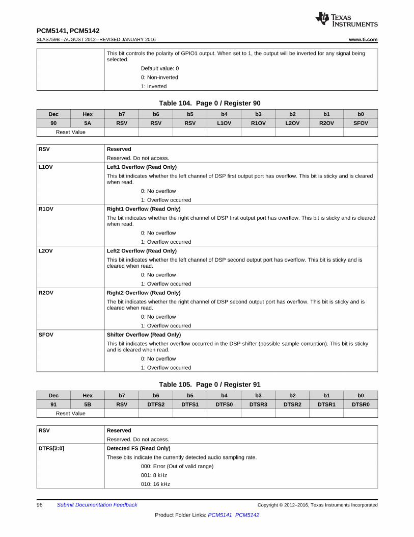
PCM5141, PCM5142SLAS759B –AUGUST 2012–REVISED JANUARY 2016 www.ti.com
This bit controls the polarity of GPIO1 output. When set to 1, the output will be inverted for any signal beingselected.
Default value: 00: Non-inverted1: Inverted
Table 104. Page 0 / Register 90Dec Hex b7 b6 b5 b4 b3 b2 b1 b090 5A RSV RSV RSV L1OV R1OV L2OV R2OV SFOV
Reset Value
RSV ReservedReserved. Do not access.
L1OV Left1 Overflow (Read Only)This bit indicates whether the left channel of DSP first output port has overflow. This bit is sticky and is clearedwhen read.
0: No overflow1: Overflow occurred
R1OV Right1 Overflow (Read Only)The bit indicates whether the right channel of DSP first output port has overflow. This bit is sticky and is clearedwhen read.
0: No overflow1: Overflow occurred
L2OV Left2 Overflow (Read Only)This bit indicates whether the left channel of DSP second output port has overflow. This bit is sticky and iscleared when read.
0: No overflow1: Overflow occurred
R2OV Right2 Overflow (Read Only)The bit indicates whether the right channel of DSP second output port has overflow. This bit is sticky and iscleared when read.
0: No overflow1: Overflow occurred
SFOV Shifter Overflow (Read Only)This bit indicates whether overflow occurred in the DSP shifter (possible sample corruption). This bit is stickyand is cleared when read.
0: No overflow1: Overflow occurred
Table 105. Page 0 / Register 91Dec Hex b7 b6 b5 b4 b3 b2 b1 b091 5B RSV DTFS2 DTFS1 DTFS0 DTSR3 DTSR2 DTSR1 DTSR0
Reset Value
RSV ReservedReserved. Do not access.
DTFS[2:0] Detected FS (Read Only)These bits indicate the currently detected audio sampling rate.
000: Error (Out of valid range)001: 8 kHz010: 16 kHz
96 Submit Documentation Feedback Copyright © 2012–2016, Texas Instruments Incorporated
Product Folder Links: PCM5141 PCM5142

PCM5141, PCM5142www.ti.com SLAS759B –AUGUST 2012–REVISED JANUARY 2016
011: 32-48 kHz100: 88.2-96 kHz101: 176.4-192 kHz110: 384 kHz
DTSR[3:0] Detected SCK Ratio (Read Only)These bits indicate the currently detected SCK ratio. Note that even if the SCK ratio is not indicated as error,clock error might still be flagged due to incompatible combination with the sampling rate. Specifically the SCKratio must be high enough to allow enough DSP cycles for minimal audio processing when PLL is disabled. Theabsolute SCK frequency must also be lower than 50 MHz.
0000: Ratio error (The SCK ratio is not allowed)0001: SCK = 32 FS0010: SCK = 48 FS0011: SCK = 64 FS0100: SCK = 128 FS0101: SCK = 192 FS0110: SCK = 256 FS0111: SCK = 384 FS1000: SCK = 512 FS1001: SCK = 768 FS1010: SCK = 1024 FS1011: SCK = 1152 FS1100: SCK = 1536 FS1101: SCK = 2048 FS1110: SCK = 3072 FS
Table 106. Page 0 / Register 92Dec Hex b7 b6 b5 b4 b3 b2 b1 b092 5C RSV RSV RSV RSV RSV RSV RSV DTBR8
Reset Value
Table 107. Page 0 / Register 93Dec Hex b7 b6 b5 b4 b3 b2 b1 b093 5D DTBR7 DTBR6 DTBR5 DTBR4 DTBR3 DTBR2 DTBR1 DTBR0
Reset Value
RSV ReservedReserved. Do not access.
DTBR[8:0] Detected BCK Ratio (MSB) (Read Only)These bits indicate the currently detected BCK ratio, that is, the number of BCK clocks in one audio frame.Note that for extreme case of BCK = 1 FS (which is not usable anyway), the detected ratio will be unreliable.
Table 108. Page 0 / Register 94Dec Hex b7 b6 b5 b4 b3 b2 b1 b094 5E RSV CDST PLL-L LrckBck fS-SCKr SCKval BCKval fSval
Reset Value
RSV ReservedReserved. Do not access.
CDST Clock Detector Status (Read Only)This bit indicates whether the SCK clock is present or not.
0: SCK is present
Copyright © 2012–2016, Texas Instruments Incorporated Submit Documentation Feedback 97
Product Folder Links: PCM5141 PCM5142

PCM5141, PCM5142SLAS759B –AUGUST 2012–REVISED JANUARY 2016 www.ti.com
1: SCK is missing (halted)PLL-L PLL locked (Read Only)
This bit indicates whether the PLL is locked or not. The PLL will be reported as unlocked when it is disabled.0: PLL is locked1: PLL is unlocked
LrckBck LRCK-BCK present (Read Only)This bit indicates whether the both LRCK and BCK are missing (tied low) or not.
0: LRCK and/or BCK is present1: LRCK and BCK are missing
fS-SCKr Sample rate SCK ratio valid (Read Only)This bit indicates whether the combination of current sampling rate and SCK ratio is valid for clock auto set.
0: The combination of FS/SCK ratio is valid1: Error (clock auto set is not possible)
SCKval SCK valid (Read Only)This bit indicates whether the SCK is valid or not. The SCK ratio must be detectable to be valid. There is alimitation with this flag, that is, when the low period of LRCK is less than or equal to 5 BCKs, this flag will beasserted (SCK invalid reported).
0: SCK is valid1: SCK is invalid
BCKval BCK valid (Read Only)This bit indicates whether the BCK is valid or not. The BCK ratio must be stable and in the range of 32-256FSto be valid.
0: BCK is valid1: BCK is invalid
fSval fS valid (Read Only)This bit indicated whether the audio sampling rate is valid or not. The sampling rate must be detectable to bevalid. There is a limitation with this flag, that is when this flag is asserted and Page 0 / Register 37 is set toignore all asserted error flags such that the DAC recovers, this flag will be de-asserted (sampling rate invalidnot reported anymore).
0: Sampling rate is valid1: Sampling rate is invalid
Table 109. Page 0 / Register 95Dec Hex b7 b6 b5 b4 b3 b2 b1 b095 5F RSV RSV RSV LTSH RSV CKMF CSRF CERF
Reset Value
RSV ReservedReserved. Do not access.
LTSH Latched Clock Halt (Read Only)This bit indicates whether SCK halt has occurred. The bit is cleared when read.
0: SCK halt has not occurred1: SCK halt has occurred since last read
CKMF Clock Missing (Read Only)This bit indicates whether the LRCK and BCK are missing (tied low).
0: LRCK and/or BCK is present1: LRCK and BCK are missing
CSRF Clock Resync Request (Read Only)This bit indicates whether the clock resynchronization is in progress.
0: Not resynchronizing1: Clock resynchronization is in progress
98 Submit Documentation Feedback Copyright © 2012–2016, Texas Instruments Incorporated
Product Folder Links: PCM5141 PCM5142
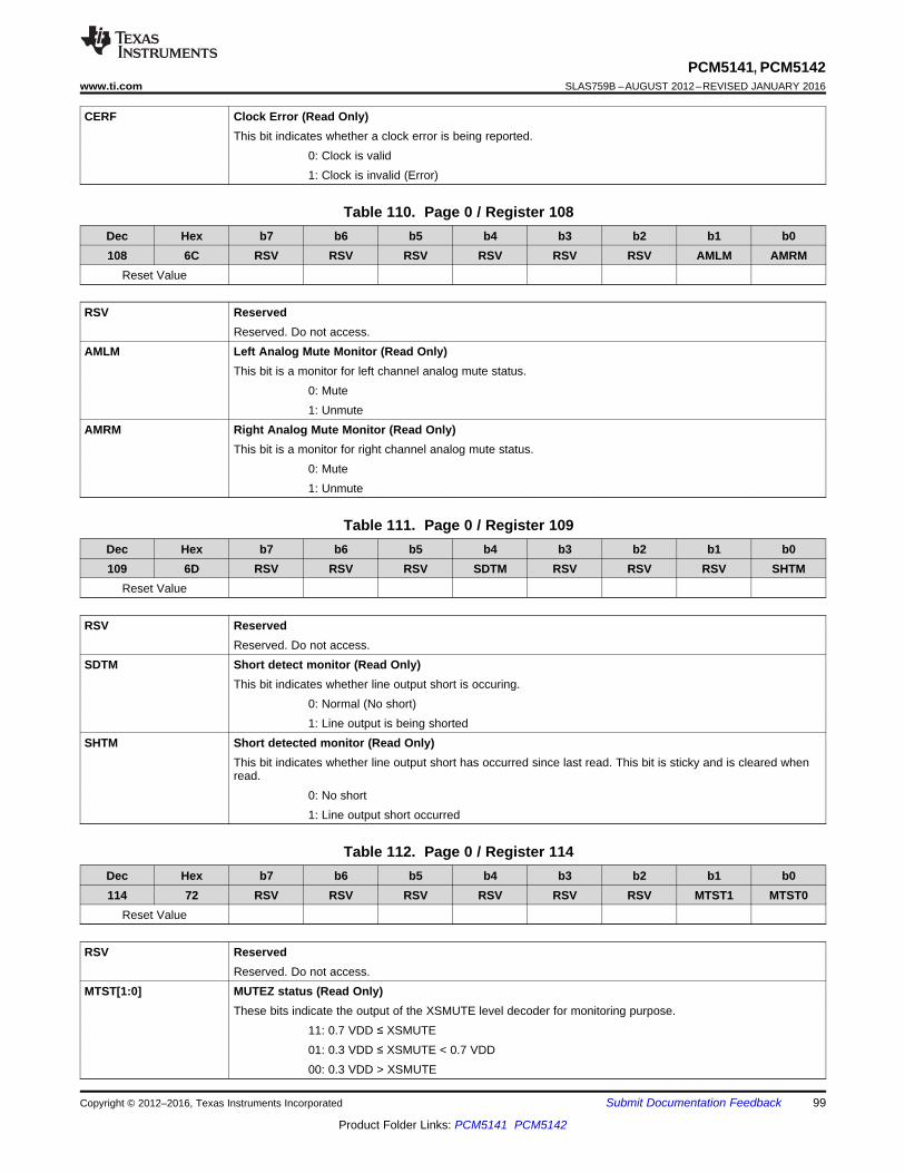
PCM5141, PCM5142www.ti.com SLAS759B –AUGUST 2012–REVISED JANUARY 2016
CERF Clock Error (Read Only)This bit indicates whether a clock error is being reported.
0: Clock is valid1: Clock is invalid (Error)
Table 110. Page 0 / Register 108Dec Hex b7 b6 b5 b4 b3 b2 b1 b0108 6C RSV RSV RSV RSV RSV RSV AMLM AMRM
Reset Value
RSV ReservedReserved. Do not access.
AMLM Left Analog Mute Monitor (Read Only)This bit is a monitor for left channel analog mute status.
0: Mute1: Unmute
AMRM Right Analog Mute Monitor (Read Only)This bit is a monitor for right channel analog mute status.
0: Mute1: Unmute
Table 111. Page 0 / Register 109Dec Hex b7 b6 b5 b4 b3 b2 b1 b0109 6D RSV RSV RSV SDTM RSV RSV RSV SHTM
Reset Value
RSV ReservedReserved. Do not access.
SDTM Short detect monitor (Read Only)This bit indicates whether line output short is occuring.
0: Normal (No short)1: Line output is being shorted
SHTM Short detected monitor (Read Only)This bit indicates whether line output short has occurred since last read. This bit is sticky and is cleared whenread.
0: No short1: Line output short occurred
Table 112. Page 0 / Register 114Dec Hex b7 b6 b5 b4 b3 b2 b1 b0114 72 RSV RSV RSV RSV RSV RSV MTST1 MTST0
Reset Value
RSV ReservedReserved. Do not access.
MTST[1:0] MUTEZ status (Read Only)These bits indicate the output of the XSMUTE level decoder for monitoring purpose.
11: 0.7 VDD ≤ XSMUTE01: 0.3 VDD ≤ XSMUTE < 0.7 VDD00: 0.3 VDD > XSMUTE
Copyright © 2012–2016, Texas Instruments Incorporated Submit Documentation Feedback 99
Product Folder Links: PCM5141 PCM5142

PCM5141, PCM5142SLAS759B –AUGUST 2012–REVISED JANUARY 2016 www.ti.com
Table 113. Page 0 / Register 115Dec Hex b7 b6 b5 b4 b3 b2 b1 b0115 73 RSV RSV RSV RSV RSV RSV FSMM1 FSMM0
Reset Value
RSV ReservedReserved. Do not access.
FSMM[1:0] FS Speed Mode Monitor (Read Only)These bits indicate the actual FS operation mode being used. The actual value is the auto set one when clockauto set is active and register set one when clock auto set is disabled.
00: Single speed (FS ≤ 48 kHz)01: Double speed (48 kHz < FS ≤ 96 kHz)10: Quad speed (96 kHz < FS ≤ 192 kHz)11: Octal speed (192 kHz < FS ≤ 384 kHz)
Table 114. Page 0 / Register 118Dec Hex b7 b6 b5 b4 b3 b2 b1 b0118 76 BOTM RSV RSV RSV PSTM3 PSTM2 PSTM1 PSTM0
Reset Value
RSV ReservedReserved. Do not access.
BOTM DSP Boot Done Flag (Read Only)This bit indicates whether the DSP boot is completed.
0: DSP is booting1: DSP boot completed
PSTM[3:0] Power State (Read Only)These bits indicate the current power state of the DAC.
0000: Powerdown0001: Wait for CP voltage valid0010: Calibration0011: Calibration0100: Volume ramp up0101: Run (Playing)0110: Line output short / Low impedance0111: Volume ramp down1000: Standby
Table 115. Page 0 / Register 119Dec Hex b7 b6 b5 b4 b3 b2 b1 b0119 77 RSV RSV GPIN5 GPIN4 GPIN3 GPIN2 GPIN1 RSV
Reset Value
RSV ReservedReserved. Do not access.
GPIN[5:0] GPIO Input States (Read Only)This bit indicates the logic level at GPIO6 pin.
0: Low1: High
100 Submit Documentation Feedback Copyright © 2012–2016, Texas Instruments Incorporated
Product Folder Links: PCM5141 PCM5142

PCM5141, PCM5142www.ti.com SLAS759B –AUGUST 2012–REVISED JANUARY 2016
Table 116. Page 0 / Register 120Dec Hex b7 b6 b5 b4 b3 b2 b1 b0120 78 RSV RSV RSV AMFL RSV RSV RSV AMFR
Reset Value
RSV ReservedReserved. Do not access.
AMFL Auto Mute Flag for Left Channel (Read Only)This bit indicates the auto mute status for left channel.
0: Not auto muted1: Auto muted
AMFR Auto Mute Flag for Right Channel (Read Only)This bit indicates the auto mute status for right channel.
0: Not auto muted1: Auto muted
Table 117. Page 0 / Register 121Dec Hex b7 b6 b5 b4 b3 b2 b1 b0121 79 RSV RSV RSV RSV RSV RSV RSV DAMD
Reset Value 0
RSV ReservedReserved. Do not access.
DAMD DAC ModeThis bit controls the DAC architecture to vary the DAC auditory signature.
Default value: 00: Mode1 - New hyper-advanced current-segment architecture1: Mode2 - Classic PCM1792 advanced current-segment architecture
Table 118. Page 0 / Register 122Dec Hex b7 b6 b5 b4 b3 b2 b1 b0122 7A RSV RSV RSV RSV RSV RSV RSV EIFM
Reset Value 0
RSV ReservedReserved. Do not access.
EIFM External Interpolation Filter ModeThis bit enables or disables the PCM1792 External Interpolation Filter Mode. This mode is used with aPCM1792 in external digital filter mode.
Default value: 00: Normal mode1: External Interpolation Filter Mode
Table 119. Page 0 / Register 123Dec Hex b7 b6 b5 b4 b3 b2 b1 b0123 7B RSV G1MC2 G1MC1 G1MC0 RSV G2MC2 G2MC1 G2MC0
Reset Value 0 0 0 0 0 0
Copyright © 2012–2016, Texas Instruments Incorporated Submit Documentation Feedback 101
Product Folder Links: PCM5141 PCM5142

PCM5141, PCM5142SLAS759B –AUGUST 2012–REVISED JANUARY 2016 www.ti.com
RSV ReservedReserved. Do not access.
G1MC[2:0] GPIO1 output for External Interpolation Filter ModeThese bits select a signal to be output to GPIO1 in External Interpolation Filter mode.
Default value: 000000: Logic low001: MS010: BCK (256FS)011: WDCK (8FS)100: DATAL101: DATAR110: Raw DIN (from DIN pin)111: Raw LRCK (from LRCK pin)
G2MC[2:0] GPIO2 output for External Interpolation Filter ModeThese bits select a signal to be output to GPIO2 in External Interpolation Filter mode.
Default value: 000000: Logic low001: MS010: BCK (256FS)011: WDCK (8FS)100: DATAL101: DATAR110: Raw DIN (from DIN pin)111: Raw LRCK (from LRCK pin)
Table 120. Page 0 / Register 124Dec Hex b7 b6 b5 b4 b3 b2 b1 b0124 7C RSV G3MC2 G3MC1 G3MC0 RSV G4MC2 G4MC1 G4MC0
Reset Value 0 0 0 0 0 0
RSV ReservedReserved. Do not access.
G3MC[2:0] GPIO3 output for External Interpolation Filter ModeThese bits select a signal to be output to GPIO3 in External Interpolation Filter Mode.
Default value: 000000: Logic low001: MS010: BCK (256FS)011: WDCK (8FS)100: DATAL101: DATAR110: Raw DIN (from DIN pin)111: Raw LRCK (from LRCK pin)
G4MC[2:0] GPIO4 output for External Interpolation Filter ModeThese bits select a signal to be output to GPIO4 in External Interpolation Filter Mode.
Default value: 000000: Logic low001: MS010: BCK (256FS)
102 Submit Documentation Feedback Copyright © 2012–2016, Texas Instruments Incorporated
Product Folder Links: PCM5141 PCM5142
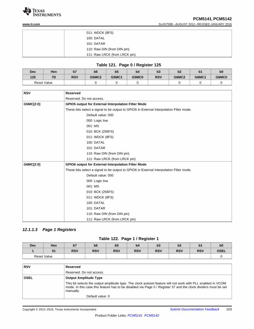
PCM5141, PCM5142www.ti.com SLAS759B –AUGUST 2012–REVISED JANUARY 2016
011: WDCK (8FS)100: DATAL101: DATAR110: Raw DIN (from DIN pin)111: Raw LRCK (from LRCK pin)
Table 121. Page 0 / Register 125Dec Hex b7 b6 b5 b4 b3 b2 b1 b0125 7D RSV G5MC2 G5MC1 G5MC0 RSV G6MC2 G6MC1 G6MC0
Reset Value 0 0 0 0 0 0
RSV ReservedReserved. Do not access.
G5MC[2:0] GPIO5 output for External Interpolation Filter ModeThese bits select a signal to be output to GPIO5 in External Interpolation Filter mode.
Default value: 000000: Logic low001: MS010: BCK (256FS)011: WDCK (8FS)100: DATAL101: DATAR110: Raw DIN (from DIN pin)111: Raw LRCK (from LRCK pin)
G6MC[2:0] GPIO6 output for External Interpolation Filter ModeThese bits select a signal to be output to GPIO6 in External Interpolation Filter mode.
Default value: 000000: Logic low001: MS010: BCK (256FS)011: WDCK (8FS)100: DATAL101: DATAR110: Raw DIN (from DIN pin)111: Raw LRCK (from LRCK pin)
12.1.1.3 Page 1 Registers
Table 122. Page 1 / Register 1Dec Hex b7 b6 b5 b4 b3 b2 b1 b0
1 01 RSV RSV RSV RSV RSV RSV RSV OSELReset Value 0
RSV ReservedReserved. Do not access.
OSEL Output Amplitude TypeThis bit selects the output amplitude type. The clock autoset feature will not work with PLL enabled in VCOMmode. In this case this feature has to be disabled via Page 0 / Register 37 and the clock dividers must be setmanually.
Default value: 0
Copyright © 2012–2016, Texas Instruments Incorporated Submit Documentation Feedback 103
Product Folder Links: PCM5141 PCM5142
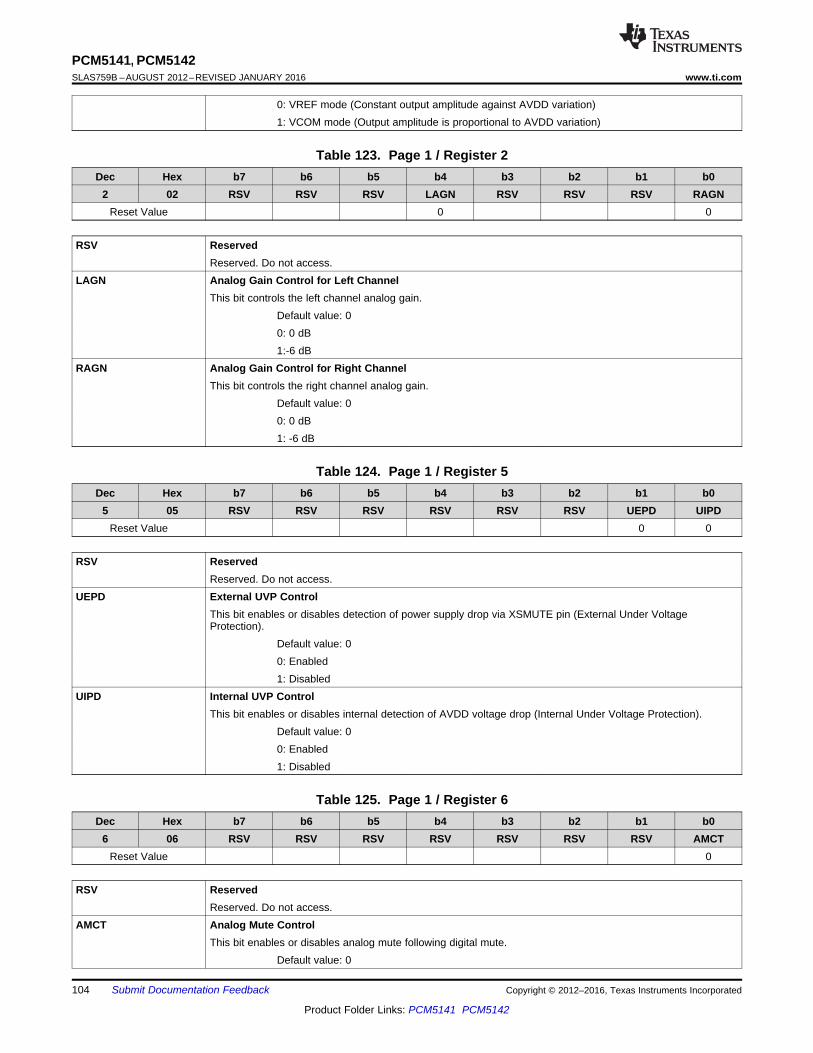
PCM5141, PCM5142SLAS759B –AUGUST 2012–REVISED JANUARY 2016 www.ti.com
0: VREF mode (Constant output amplitude against AVDD variation)1: VCOM mode (Output amplitude is proportional to AVDD variation)
Table 123. Page 1 / Register 2Dec Hex b7 b6 b5 b4 b3 b2 b1 b0
2 02 RSV RSV RSV LAGN RSV RSV RSV RAGNReset Value 0 0
RSV ReservedReserved. Do not access.
LAGN Analog Gain Control for Left ChannelThis bit controls the left channel analog gain.
Default value: 00: 0 dB1:-6 dB
RAGN Analog Gain Control for Right ChannelThis bit controls the right channel analog gain.
Default value: 00: 0 dB1: -6 dB
Table 124. Page 1 / Register 5Dec Hex b7 b6 b5 b4 b3 b2 b1 b0
5 05 RSV RSV RSV RSV RSV RSV UEPD UIPDReset Value 0 0
RSV ReservedReserved. Do not access.
UEPD External UVP ControlThis bit enables or disables detection of power supply drop via XSMUTE pin (External Under VoltageProtection).
Default value: 00: Enabled1: Disabled
UIPD Internal UVP ControlThis bit enables or disables internal detection of AVDD voltage drop (Internal Under Voltage Protection).
Default value: 00: Enabled1: Disabled
Table 125. Page 1 / Register 6Dec Hex b7 b6 b5 b4 b3 b2 b1 b0
6 06 RSV RSV RSV RSV RSV RSV RSV AMCTReset Value 0
RSV ReservedReserved. Do not access.
AMCT Analog Mute ControlThis bit enables or disables analog mute following digital mute.
Default value: 0
104 Submit Documentation Feedback Copyright © 2012–2016, Texas Instruments Incorporated
Product Folder Links: PCM5141 PCM5142

PCM5141, PCM5142www.ti.com SLAS759B –AUGUST 2012–REVISED JANUARY 2016
0: Enabled1: Disabled
Table 126. Page 1 / Register 7Dec Hex b7 b6 b5 b4 b3 b2 b1 b0
7 07 RSV RSV RSV AGBL RSV RSV RSV AGBRReset Value 0 0
RSV ReservedReserved. Do not access.
AGBL Analog +10% Gain for Left ChannelThis bit enables or disables amplitude boost mode for left channel.
Default value: 00: Normal amplitude1: +10% (+0.8 dB) boosted amplitude
AGBR Analog +10% Gain for Right ChannelThis bit enables or disables amplitude boost mode for right channel.
Default value: 00: Normal amplitude1: +10% (+0.8 dB) boosted amplitude
Table 127. Page 1 / Register 8Dec Hex b7 b6 b5 b4 b3 b2 b1 b0
8 08 RSV RSV RSV RSV RSV RSV RSV RCMFReset Value 0
RSV ReservedReserved. Do not access.
RCMF VCOM Reference Ramp UpThis bit controls the VCOM voltage ramp up speed.
Default value: 00: Normal ramp up, ~600ms with external capacitance = 1uF1: Fast ramp up, ~3ms with external capacitance = 1uF
Table 128. Page 1 / Register 9Dec Hex b7 b6 b5 b4 b3 b2 b1 b0
9 09 RSV RSV RSV RSV RSV RSV RSV VCPDReset Value 1
RSV ReservedReserved. Do not access.
VCPD Power down control for VCOMThis bit controls VCOM powerdown switch.
Default value: 10: VCOM is powered on1: VCOM is powered down
Copyright © 2012–2016, Texas Instruments Incorporated Submit Documentation Feedback 105
Product Folder Links: PCM5141 PCM5142

PCM5141, PCM5142SLAS759B –AUGUST 2012–REVISED JANUARY 2016 www.ti.com
12.1.1.4 Page 44 Registers
Table 129. Page 44 / Register 1Dec Hex b7 b6 b5 b4 b3 b2 b1 b0
1 01 RSV RSV RSV RSV ACRM AMDC ACRS ACSWReset Value 0 0
RSV ReservedReserved. Do not access.
ACRM Active CRAM Monitor (Read Only)This bit indicates which CRAM is being accessed by the DSP when adaptive mode is disabled. When adaptivemode is enabled, this bit has no meaning.
0: CRAM A is being used by the DSP1: CRAM B is being used by the DSP
AMDC Adaptive Mode ControlThis bit controls the DSP adaptive mode. When in adaptive mode, only CRAM A is accessible via serialinterface when the DSP is disabled (DAC in standby state), while when the DSP is enabled (DAC is run state)the CRAM A can only be accessed by the DSP and the CRAM B can only be accessed by the serial interface,or vice versa depending on the value of CRAMSTAT. When not in adaptive mode, both CRAM A and B can beaccessed by the serial interface when the DSP is disabled, but when the DSP is enabled, no CRAM can beaccessed by serial interface. The DSP can access either CRAM, which can be monitored at SWPMON.
Default value: 00: Adaptive mode disabled1: Adaptive mode enabled
ACRS Active CRAM Selection (Read Only)This bit indicates which CRAM currently serves as the active one. The other CRAM serves as an update buffer,and can accessed by serial interface (SPI/I2C)
0: CRAM A is active and being used by the DSP1: CRAM B is active and being used by the DSP
ACSW Switch Active CRAMThis bit is used to request switching roles of the two buffers, that is, switching the active buffer role betweenCRAM A and CRAM B. This bit is cleared automatically when the switching process completed.
Default value: 00: No switching requested or switching completed1: Switching is being requested
12.1.1.5 Page 253 Registers
Table 130. Page 253 / Register 63Dec Hex b7 b6 b5 b4 b3 b2 b1 b063 3F PLLFLEX1 PLLFLEX1 PLLFLEX1 PLLFLEX1 PLLFLEX1 PLLFLEX1 PLLFLEX1 PLLFLEX1
7 6 5 4 3 2 1 0Reset Value 0 0 0 0 0 0 0 0
PLLFLEX1[7:0] Clock Flex Register #1Clock Flex Register #1. Write 0x11 to this register to allow advanced clock tree functions. See ClockingOverview section.
Default value: 00000000
106 Submit Documentation Feedback Copyright © 2012–2016, Texas Instruments Incorporated
Product Folder Links: PCM5141 PCM5142

PCM5141, PCM5142www.ti.com SLAS759B –AUGUST 2012–REVISED JANUARY 2016
Table 131. Page 253 / Register 64Dec Hex b7 b6 b5 b4 b3 b2 b1 b064 40 PLLFLEX2 PLLFLEX2 PLLFLEX2 PLLFLEX2 PLLFLEX2 PLLFLEX2 PLLFLEX2 PLLFLEX2
7 6 5 4 3 2 1 0Reset Value 0 0 0 0 0 0 0 0
PLLFLEX2[7:0] Clock Flex Register #2Clock Flex Register #2. Write 0xFF to this register to allow advanced clock tree functions. See ClockingOverview section.
Default value: 00000000
Copyright © 2012–2016, Texas Instruments Incorporated Submit Documentation Feedback 107
Product Folder Links: PCM5141 PCM5142

PCM5141, PCM5142SLAS759B –AUGUST 2012–REVISED JANUARY 2016 www.ti.com
12.1.2 PLL Tables for Software Controlled Devices
Table 132. Recommended Clock Divider Settings for PLL as Master Clock (VREF Mode)PLL VCO MOD FfS (kHz) RSCK SCK (MHz) P PLL REF (MHz) M = K*R K = J.D R PLL fS DSP fS NMAC DSP CLK (MHz) MOD fS NDAC DOSR % ERROR NCP CP F (kHz)(MHz) (kHz)
8 128 1.024 98.304 1 1.024 96 48 2 12288 1024 12 8.192 768 6144 16 48 0 4 1536
8 192 1.536 98.304 1 1.536 64 32 2 12288 1024 12 8.192 768 6144 16 48 0 4 1536
8 256 2.048 98.304 1 2.048 48 48 1 12288 1024 12 8.192 768 6144 16 48 0 4 1536
8 384 3.072 98.304 3 1.024 96 48 2 12288 1024 12 8.192 768 6144 16 48 0 4 1536
8 512 4.096 98.304 3 1.365 72 36 2 12288 1024 12 8.192 768 6144 16 48 0 4 1536
8 768 6.144 98.304 3 2.048 48 48 1 12288 1024 12 8.192 768 6144 16 48 0 4 1536
8 1024 8.192 98.304 3 2.731 36 36 1 12288 1024 12 8.192 768 6144 16 48 0 4 1536
8 1152 9.216 98.304 9 1.024 96 48 2 12288 1024 12 8.192 768 6144 16 48 0 4 1536
8 1536 12.288 98.304 9 1.365 72 36 2 12288 1024 12 8.192 768 6144 16 48 0 4 1536
8 2048 16.384 98.304 9 1.82 54 54 1 12288 1024 12 8.192 768 6144 16 48 0 4 1536
8 3072 24.576 98.304 9 2.731 36 36 1 12288 1024 12 8.192 768 6144 16 48 0 4 1536
11.025 128 1.4112 90.3168 1 1.411 64 32 2 8192 1024 8 11.2896 512 5644.8 16 32 0 4 1411.2
11.025 192 2.1168 90.3168 3 0.706 128 32 4 8192 1024 8 11.2896 512 5644.8 16 32 0 4 1411.2
11.025 256 2.8224 90.3168 1 2.822 32 32 1 8192 1024 8 11.2896 512 5644.8 16 32 0 4 1411.2
11.025 384 4.2336 90.3168 3 1.411 64 32 2 8192 1024 8 11.2896 512 5644.8 16 32 0 4 1411.2
11.025 512 5.6448 90.3168 3 1.882 48 48 1 8192 1024 8 11.2896 512 5644.8 16 32 0 4 1411.2
11.025 768 8.4672 90.3168 3 2.822 32 32 1 8192 1024 8 11.2896 512 5644.8 16 32 0 4 1411.2
11.025 1024 11.2896 90.3168 3 3.763 24 24 1 8192 1024 8 11.2896 512 5644.8 16 32 0 4 1411.2
11.025 1152 12.7008 90.3168 9 1.411 64 32 2 8192 1024 8 11.2896 512 5644.8 16 32 0 4 1411.2
11.025 1536 16.9344 90.3168 9 1.882 48 48 1 8192 1024 8 11.2896 512 5644.8 16 32 0 4 1411.2
11.025 2048 22.5792 90.3168 9 2.509 36 36 1 8192 1024 8 11.2896 512 5644.8 16 32 0 4 1411.2
11.025 3072 33.8688 90.3168 9 3.763 24 24 1 8192 1024 8 11.2896 512 5644.8 16 32 0 4 1411.2
16 64 1.024 98.304 1 1.024 96 48 2 6144 1024 6 16.384 384 6144 16 24 0 4 1536
16 128 2.048 98.304 1 2.048 48 48 1 6144 1024 6 16.384 384 6144 16 24 0 4 1536
16 192 3.072 98.304 1 3.072 32 32 1 6144 1024 6 16.384 384 6144 16 24 0 4 1536
16 256 4.096 98.304 1 4.096 24 24 1 6144 1024 6 16.384 384 6144 16 24 0 4 1536
16 384 6.144 98.304 3 2.048 48 48 1 6144 1024 6 16.384 384 6144 16 24 0 4 1536
16 512 8.192 98.304 3 2.731 36 36 1 6144 1024 6 16.384 384 6144 16 24 0 4 1536
16 768 12.288 98.304 3 4.096 24 24 1 6144 1024 6 16.384 384 6144 16 24 0 4 1536
16 1024 16.384 98.304 3 5.461 18 18 1 6144 1024 6 16.384 384 6144 16 24 0 4 1536
16 1152 18.432 98.304 3 6.144 16 16 1 6144 1024 6 16.384 384 6144 16 24 0 4 1536
16 1536 24.576 98.304 9 2.731 36 36 1 6144 1024 6 16.384 384 6144 16 24 0 4 1536
16 2048 32.768 98.304 9 3.641 27 27 1 6144 1024 6 16.384 384 6144 16 24 0 4 1536
16 3072 49.152 98.304 9 5.461 18 18 1 6144 1024 6 16.384 384 6144 16 24 0 4 1536
22.05 64 1.4112 90.3168 1 1.411 64 32 2 4096 1024 4 22.5792 256 5644.8 16 16 0 4 1411.2
22.05 128 2.8224 90.3168 1 2.822 32 32 1 4096 1024 4 22.5792 256 5644.8 16 16 0 4 1411.2
108 Submit Documentation Feedback Copyright © 2012–2016, Texas Instruments Incorporated
Product Folder Links: PCM5141 PCM5142

PCM5141, PCM5142www.ti.com SLAS759B –AUGUST 2012–REVISED JANUARY 2016
Table 132. Recommended Clock Divider Settings for PLL as Master Clock (VREF Mode) (continued)PLL VCO MOD FfS (kHz) RSCK SCK (MHz) P PLL REF (MHz) M = K*R K = J.D R PLL fS DSP fS NMAC DSP CLK (MHz) MOD fS NDAC DOSR % ERROR NCP CP F (kHz)(MHz) (kHz)
22.05 192 4.2336 90.3168 3 1.411 64 32 2 4096 1024 4 22.5792 256 5644.8 16 16 0 4 1411.2
22.05 256 5.6448 90.3168 1 5.645 16 16 1 4096 1024 4 22.5792 256 5644.8 16 16 0 4 1411.2
22.05 384 8.4672 90.3168 3 2.822 32 32 1 4096 1024 4 22.5792 256 5644.8 16 16 0 4 1411.2
22.05 512 11.2896 90.3168 3 3.763 24 24 1 4096 1024 4 22.5792 256 5644.8 16 16 0 4 1411.2
22.05 768 16.9344 90.3168 3 5.645 16 16 1 4096 1024 4 22.5792 256 5644.8 16 16 0 4 1411.2
22.05 1024 22.5792 90.3168 3 7.526 12 12 1 4096 1024 4 22.5792 256 5644.8 16 16 0 4 1411.2
22.05 1152 25.4016 90.3168 9 2.822 32 32 1 4096 1024 4 22.5792 256 5644.8 16 16 0 4 1411.2
22.05 1536 33.8688 90.3168 9 3.763 24 24 1 4096 1024 4 22.5792 256 5644.8 16 16 0 4 1411.2
22.05 2048 45.1584 90.3168 9 5.018 18 18 1 4096 1024 4 22.5792 256 5644.8 16 16 0 4 1411.2
32 32 1.024 98.304 1 1.024 96 48 2 3072 1024 3 32.768 192 6144 16 12 0 4 1536
32 48 1.536 98.304 1 1.536 64 16 4 3072 1024 3 32.768 192 6144 16 12 0 4 1536
32 64 2.048 98.304 1 2.048 48 24 2 3072 1024 3 32.768 192 6144 16 12 0 4 1536
32 128 4.096 98.304 1 4.096 24 24 1 3072 1024 3 32.768 192 6144 16 12 0 4 1536
32 192 6.144 98.304 3 2.048 48 48 1 3072 1024 3 32.768 192 6144 16 12 0 4 1536
32 256 8.192 98.304 2 4.096 24 24 1 3072 1024 3 32.768 192 6144 16 12 0 4 1536
32 384 12.288 98.304 3 4.096 24 24 1 3072 1024 3 32.768 192 6144 16 12 0 4 1536
32 512 16.384 98.304 3 5.461 18 18 1 3072 1024 3 32.768 192 6144 16 12 0 4 1536
32 768 24.576 98.304 3 8.192 12 12 1 3072 1024 3 32.768 192 6144 16 12 0 4 1536
32 1024 32.768 98.304 3 10.923 9 9 1 3072 1024 3 32.768 192 6144 16 12 0 4 1536
32 1152 36.864 98.304 9 4.096 24 24 1 3072 1024 3 32.768 192 6144 16 12 0 4 1536
32 1536 49.152 98.304 6 8.192 12 12 1 3072 1024 3 32.768 192 6144 16 12 0 4 1536
44.1 32 1.4112 90.3168 1 1.411 64 32 2 2048 1024 2 45.1584 128 5644.8 16 8 0 4 1411.2
44.1 64 2.8224 90.3168 1 2.822 32 16 2 2048 1024 2 45.1584 128 5644.8 16 8 0 4 1411.2
44.1 128 5.6448 90.3168 1 5.645 16 16 1 2048 1024 2 45.1584 128 5644.8 16 8 0 4 1411.2
44.1 192 8.4672 90.3168 3 2.822 32 32 1 2048 1024 2 45.1584 128 5644.8 16 8 0 4 1411.2
44.1 256 11.2896 90.3168 2 5.645 16 16 1 2048 1024 2 45.1584 128 5644.8 16 8 0 4 1411.2
44.1 384 16.9344 90.3168 3 5.645 16 16 1 2048 1024 2 45.1584 128 5644.8 16 8 0 4 1411.2
44.1 512 22.5792 90.3168 3 7.526 12 12 1 2048 1024 2 45.1584 128 5644.8 16 8 0 4 1411.2
44.1 768 33.8688 90.3168 3 11.29 8 8 1 2048 1024 2 45.1584 128 5644.8 16 8 0 4 1411.2
44.1 1024 45.1584 90.3168 3 15.053 6 6 1 2048 1024 2 45.1584 128 5644.8 16 8 0 4 1411.2
48 32 1.536 98.304 1 1.536 64 32 2 2048 1024 2 49.152 128 6144 16 8 0 4 1536
48 64 3.072 98.304 1 3.072 32 16 2 2048 1024 2 49.152 128 6144 16 8 0 4 1536
48 128 6.144 98.304 1 6.144 16 16 1 2048 1024 2 49.152 128 6144 16 8 0 4 1536
48 192 9.216 98.304 3 3.072 32 32 1 2048 1024 2 49.152 128 6144 16 8 0 4 1536
48 256 12.288 98.304 2 6.144 16 16 1 2048 1024 2 49.152 128 6144 16 8 0 4 1536
48 384 18.432 98.304 3 6.144 16 16 1 2048 1024 2 49.152 128 6144 16 8 0 4 1536
48 512 24.576 98.304 3 8.192 12 12 1 2048 1024 2 49.152 128 6144 16 8 0 4 1536
48 768 36.864 98.304 3 12.288 8 8 1 2048 1024 2 49.152 128 6144 16 8 0 4 1536
Copyright © 2012–2016, Texas Instruments Incorporated Submit Documentation Feedback 109
Product Folder Links: PCM5141 PCM5142

PCM5141, PCM5142SLAS759B –AUGUST 2012–REVISED JANUARY 2016 www.ti.com
Table 132. Recommended Clock Divider Settings for PLL as Master Clock (VREF Mode) (continued)PLL VCO MOD FfS (kHz) RSCK SCK (MHz) P PLL REF (MHz) M = K*R K = J.D R PLL fS DSP fS NMAC DSP CLK (MHz) MOD fS NDAC DOSR % ERROR NCP CP F (kHz)(MHz) (kHz)
48 1024 49.152 98.304 3 16.384 6 6 1 2048 1024 2 49.152 128 6144 16 8 0 4 1536
96 32 3.072 98.304 1 3.072 32 16 2 1024 512 2 49.152 64 6144 16 4 0 4 1536
96 48 4.608 98.304 3 1.536 64 32 2 1024 512 2 49.152 64 6144 16 4 0 4 1536
96 64 6.144 98.304 1 6.144 16 8 2 1024 512 2 49.152 64 6144 16 4 0 4 1536
96 128 12.288 98.304 2 6.144 16 16 1 1024 512 2 49.152 64 6144 16 4 0 4 1536
96 192 18.432 98.304 3 6.144 16 16 1 1024 512 2 49.152 64 6144 16 4 0 4 1536
96 256 24.576 98.304 4 6.144 16 16 1 1024 512 2 49.152 64 6144 16 4 0 4 1536
96 384 36.864 98.304 6 6.144 16 16 1 1024 512 2 49.152 64 6144 16 4 0 4 1536
96 512 49.152 98.304 8 6.144 16 16 1 1024 512 2 49.152 64 6144 16 4 0 4 1536
192 32 6.144 98.304 1 6.144 16 8 2 512 256 2 49.152 32 6144 16 2 0 4 1536
192 48 9.216 98.304 3 3.072 32 16 2 512 256 2 49.152 32 6144 16 2 0 4 1536
192 64 12.288 98.304 1 12.288 8 4 2 512 256 2 49.152 32 6144 16 2 0 4 1536
192 128 24.576 98.304 2 12.288 8 8 1 512 256 2 49.152 32 6144 16 2 0 4 1536
192 192 36.864 98.304 3 12.288 8 8 1 512 256 2 49.152 32 6144 16 2 0 4 1536
192 256 49.152 98.304 4 12.288 8 8 1 512 256 2 49.152 32 6144 16 2 0 4 1536
384 32 12.288 98.304 2 6.144 16 8 2 256 128 2 49.152 16 6144 16 1 0 4 1536
384 48 18.432 98.304 3 6.144 16 8 2 256 128 2 49.152 16 6144 16 1 0 4 1536
384 64 24.576 98.304 2 12.288 8 4 2 256 128 2 49.152 16 6144 16 1 0 4 1536
384 128 49.152 98.304 4 12.288 8 8 1 256 128 2 49.152 16 6144 16 1 0 4 1536
110 Submit Documentation Feedback Copyright © 2012–2016, Texas Instruments Incorporated
Product Folder Links: PCM5141 PCM5142

PCM5141, PCM5142www.ti.com SLAS759B –AUGUST 2012–REVISED JANUARY 2016
Table 133. Recommended Clock Divider Settings for PLL as Master Clock (VCOM Mode)SCK PLL VCO PLL REF DSP CLK MOD F CP FfS (kHz) RSCK P M = K*R K = J.D R PLL fS DSP fS NMAC MOD fS NDAC DOSR % ERROR NCP(MHz) (MHz) (MHz) (MHz) (kHz) (kHz)
8 128 1.024 73.728 1 1.024 72 36 2 9216 768 12 6.144 768 6144 12 48 0 4 1536
8 192 1.536 73.728 1 1.536 48 24 2 9216 768 12 6.144 768 6144 12 48 0 4 1536
8 256 2.048 73.728 1 2.048 36 36 1 9216 768 12 6.144 768 6144 12 48 0 4 1536
8 384 3.072 73.728 1 3.072 24 12 2 9216 768 12 6.144 768 6144 12 48 0 4 1536
8 512 4.096 73.728 2 2.048 36 36 1 9216 768 12 6.144 768 6144 12 48 0 4 1536
8 768 6.144 73.728 3 2.048 36 36 1 9216 768 12 6.144 768 6144 12 48 0 4 1536
8 1024 8.192 73.728 4 2.048 36 36 1 9216 768 12 6.144 768 6144 12 48 0 4 1536
8 1152 9.216 73.728 6 1.536 48 48 1 9216 768 12 6.144 768 6144 12 48 0 4 1536
8 1536 12.288 73.728 6 2.048 36 36 1 9216 768 12 6.144 768 6144 12 48 0 4 1536
8 2048 16.384 73.728 8 2.048 36 36 1 9216 768 12 6.144 768 6144 12 48 0 4 1536
8 3072 24.576 73.728 12 2.048 36 36 1 9216 768 12 6.144 768 6144 12 48 0 4 1536
11.025 128 1.4112 84.672 1 1.411 60 30 2 7680 960 8 10.584 512 5644.8 15 32 0 4 1411.2
11.025 192 2.1168 84.672 1 2.117 40 10 4 7680 960 8 10.584 512 5644.8 15 32 0 4 1411.2
11.025 256 2.8224 84.672 1 2.822 30 30 1 7680 960 8 10.584 512 5644.8 15 32 0 4 1411.2
11.025 384 4.2336 84.672 2 2.117 40 20 2 7680 960 8 10.584 512 5644.8 15 32 0 4 1411.2
11.025 512 5.6448 84.672 2 2.822 30 30 1 7680 960 8 10.584 512 5644.8 15 32 0 4 1411.2
11.025 768 8.4672 84.672 3 2.822 30 30 1 7680 960 8 10.584 512 5644.8 15 32 0 4 1411.2
11.025 1024 11.2896 84.672 4 2.822 30 30 1 7680 960 8 10.584 512 5644.8 15 32 0 4 1411.2
11.025 1152 12.7008 84.672 6 2.117 40 20 2 7680 960 8 10.584 512 5644.8 15 32 0 4 1411.2
11.025 1536 16.9344 84.672 8 2.117 40 40 1 7680 960 8 10.584 512 5644.8 15 32 0 4 1411.2
11.025 2048 22.5792 84.672 8 2.822 30 30 1 7680 960 8 10.584 512 5644.8 15 32 0 4 1411.2
11.025 3072 33.8688 84.672 8 4.234 20 20 1 7680 960 8 10.584 512 5644.8 15 32 0 4 1411.2
16 64 1.024 73.728 1 1.024 72 36 2 4608 768 6 12.288 384 6144 12 24 0 4 1536
16 128 2.048 73.728 1 2.048 36 36 1 4608 768 6 12.288 384 6144 12 24 0 4 1536
16 192 3.072 73.728 1 3.072 24 24 1 4608 768 6 12.288 384 6144 12 24 0 4 1536
16 256 4.096 73.728 2 2.048 36 36 1 4608 768 6 12.288 384 6144 12 24 0 4 1536
16 384 6.144 73.728 3 2.048 36 36 1 4608 768 6 12.288 384 6144 12 24 0 4 1536
16 512 8.192 73.728 4 2.048 36 36 1 4608 768 6 12.288 384 6144 12 24 0 4 1536
16 768 12.288 73.728 6 2.048 36 36 1 4608 768 6 12.288 384 6144 12 24 0 4 1536
16 1024 16.384 73.728 8 2.048 36 36 1 4608 768 6 12.288 384 6144 12 24 0 4 1536
16 1152 18.432 73.728 9 2.048 36 36 1 4608 768 6 12.288 384 6144 12 24 0 4 1536
16 1536 24.576 73.728 8 3.072 24 24 1 4608 768 6 12.288 384 6144 12 24 0 4 1536
16 2048 32.768 73.728 8 4.096 18 18 1 4608 768 6 12.288 384 6144 12 24 0 4 1536
16 3072 49.152 73.728 8 6.144 12 12 1 4608 768 6 12.288 384 6144 12 24 0 4 1536
22.05 64 1.4112 84.672 1 1.411 60 30 2 3840 960 4 21.168 256 5644.8 15 16 0 4 1411.2
22.05 128 2.8224 84.672 1 2.822 30 30 1 3840 960 4 21.168 256 5644.8 15 16 0 4 1411.2
22.05 192 4.2336 84.672 3 1.411 60 30 2 3840 960 4 21.168 256 5644.8 15 16 0 4 1411.2
22.05 256 5.6448 84.672 2 2.822 30 30 1 3840 960 4 21.168 256 5644.8 15 16 0 4 1411.2
Copyright © 2012–2016, Texas Instruments Incorporated Submit Documentation Feedback 111
Product Folder Links: PCM5141 PCM5142
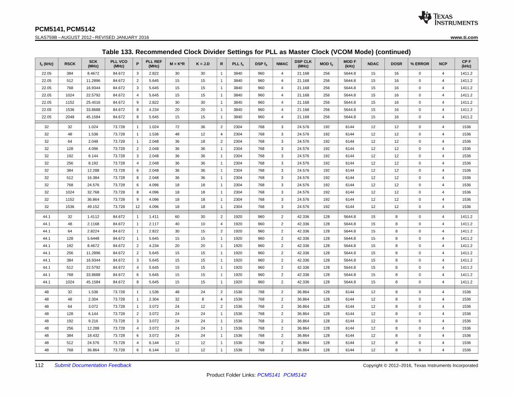
PCM5141, PCM5142SLAS759B –AUGUST 2012–REVISED JANUARY 2016 www.ti.com
Table 133. Recommended Clock Divider Settings for PLL as Master Clock (VCOM Mode) (continued)SCK PLL VCO PLL REF DSP CLK MOD F CP FfS (kHz) RSCK P M = K*R K = J.D R PLL fS DSP fS NMAC MOD fS NDAC DOSR % ERROR NCP(MHz) (MHz) (MHz) (MHz) (kHz) (kHz)
22.05 384 8.4672 84.672 3 2.822 30 30 1 3840 960 4 21.168 256 5644.8 15 16 0 4 1411.2
22.05 512 11.2896 84.672 2 5.645 15 15 1 3840 960 4 21.168 256 5644.8 15 16 0 4 1411.2
22.05 768 16.9344 84.672 3 5.645 15 15 1 3840 960 4 21.168 256 5644.8 15 16 0 4 1411.2
22.05 1024 22.5792 84.672 4 5.645 15 15 1 3840 960 4 21.168 256 5644.8 15 16 0 4 1411.2
22.05 1152 25.4016 84.672 9 2.822 30 30 1 3840 960 4 21.168 256 5644.8 15 16 0 4 1411.2
22.05 1536 33.8688 84.672 8 4.234 20 20 1 3840 960 4 21.168 256 5644.8 15 16 0 4 1411.2
22.05 2048 45.1584 84.672 8 5.645 15 15 1 3840 960 4 21.168 256 5644.8 15 16 0 4 1411.2
32 32 1.024 73.728 1 1.024 72 36 2 2304 768 3 24.576 192 6144 12 12 0 4 1536
32 48 1.536 73.728 1 1.536 48 12 4 2304 768 3 24.576 192 6144 12 12 0 4 1536
32 64 2.048 73.728 1 2.048 36 18 2 2304 768 3 24.576 192 6144 12 12 0 4 1536
32 128 4.096 73.728 2 2.048 36 36 1 2304 768 3 24.576 192 6144 12 12 0 4 1536
32 192 6.144 73.728 3 2.048 36 36 1 2304 768 3 24.576 192 6144 12 12 0 4 1536
32 256 8.192 73.728 4 2.048 36 36 1 2304 768 3 24.576 192 6144 12 12 0 4 1536
32 384 12.288 73.728 6 2.048 36 36 1 2304 768 3 24.576 192 6144 12 12 0 4 1536
32 512 16.384 73.728 8 2.048 36 36 1 2304 768 3 24.576 192 6144 12 12 0 4 1536
32 768 24.576 73.728 6 4.096 18 18 1 2304 768 3 24.576 192 6144 12 12 0 4 1536
32 1024 32.768 73.728 8 4.096 18 18 1 2304 768 3 24.576 192 6144 12 12 0 4 1536
32 1152 36.864 73.728 9 4.096 18 18 1 2304 768 3 24.576 192 6144 12 12 0 4 1536
32 1536 49.152 73.728 12 4.096 18 18 1 2304 768 3 24.576 192 6144 12 12 0 4 1536
44.1 32 1.4112 84.672 1 1.411 60 30 2 1920 960 2 42.336 128 5644.8 15 8 0 4 1411.2
44.1 48 2.1168 84.672 1 2.117 40 10 4 1920 960 2 42.336 128 5644.8 15 8 0 4 1411.2
44.1 64 2.8224 84.672 1 2.822 30 15 2 1920 960 2 42.336 128 5644.8 15 8 0 4 1411.2
44.1 128 5.6448 84.672 1 5.645 15 15 1 1920 960 2 42.336 128 5644.8 15 8 0 4 1411.2
44.1 192 8.4672 84.672 2 4.234 20 20 1 1920 960 2 42.336 128 5644.8 15 8 0 4 1411.2
44.1 256 11.2896 84.672 2 5.645 15 15 1 1920 960 2 42.336 128 5644.8 15 8 0 4 1411.2
44.1 384 16.9344 84.672 3 5.645 15 15 1 1920 960 2 42.336 128 5644.8 15 8 0 4 1411.2
44.1 512 22.5792 84.672 4 5.645 15 15 1 1920 960 2 42.336 128 5644.8 15 8 0 4 1411.2
44.1 768 33.8688 84.672 6 5.645 15 15 1 1920 960 2 42.336 128 5644.8 15 8 0 4 1411.2
44.1 1024 45.1584 84.672 8 5.645 15 15 1 1920 960 2 42.336 128 5644.8 15 8 0 4 1411.2
48 32 1.536 73.728 1 1.536 48 24 2 1536 768 2 36.864 128 6144 12 8 0 4 1536
48 48 2.304 73.728 1 2.304 32 8 4 1536 768 2 36.864 128 6144 12 8 0 4 1536
48 64 3.072 73.728 1 3.072 24 12 2 1536 768 2 36.864 128 6144 12 8 0 4 1536
48 128 6.144 73.728 2 3.072 24 24 1 1536 768 2 36.864 128 6144 12 8 0 4 1536
48 192 9.216 73.728 3 3.072 24 24 1 1536 768 2 36.864 128 6144 12 8 0 4 1536
48 256 12.288 73.728 4 3.072 24 24 1 1536 768 2 36.864 128 6144 12 8 0 4 1536
48 384 18.432 73.728 6 3.072 24 24 1 1536 768 2 36.864 128 6144 12 8 0 4 1536
48 512 24.576 73.728 4 6.144 12 12 1 1536 768 2 36.864 128 6144 12 8 0 4 1536
48 768 36.864 73.728 6 6.144 12 12 1 1536 768 2 36.864 128 6144 12 8 0 4 1536
112 Submit Documentation Feedback Copyright © 2012–2016, Texas Instruments Incorporated
Product Folder Links: PCM5141 PCM5142
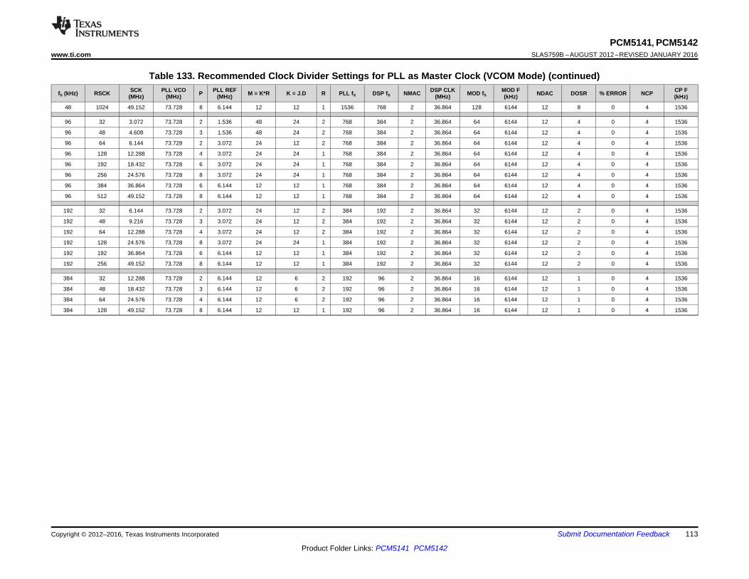
PCM5141, PCM5142www.ti.com SLAS759B –AUGUST 2012–REVISED JANUARY 2016
Table 133. Recommended Clock Divider Settings for PLL as Master Clock (VCOM Mode) (continued)SCK PLL VCO PLL REF DSP CLK MOD F CP FfS (kHz) RSCK P M = K*R K = J.D R PLL fS DSP fS NMAC MOD fS NDAC DOSR % ERROR NCP(MHz) (MHz) (MHz) (MHz) (kHz) (kHz)
48 1024 49.152 73.728 8 6.144 12 12 1 1536 768 2 36.864 128 6144 12 8 0 4 1536
96 32 3.072 73.728 2 1.536 48 24 2 768 384 2 36.864 64 6144 12 4 0 4 1536
96 48 4.608 73.728 3 1.536 48 24 2 768 384 2 36.864 64 6144 12 4 0 4 1536
96 64 6.144 73.728 2 3.072 24 12 2 768 384 2 36.864 64 6144 12 4 0 4 1536
96 128 12.288 73.728 4 3.072 24 24 1 768 384 2 36.864 64 6144 12 4 0 4 1536
96 192 18.432 73.728 6 3.072 24 24 1 768 384 2 36.864 64 6144 12 4 0 4 1536
96 256 24.576 73.728 8 3.072 24 24 1 768 384 2 36.864 64 6144 12 4 0 4 1536
96 384 36.864 73.728 6 6.144 12 12 1 768 384 2 36.864 64 6144 12 4 0 4 1536
96 512 49.152 73.728 8 6.144 12 12 1 768 384 2 36.864 64 6144 12 4 0 4 1536
192 32 6.144 73.728 2 3.072 24 12 2 384 192 2 36.864 32 6144 12 2 0 4 1536
192 48 9.216 73.728 3 3.072 24 12 2 384 192 2 36.864 32 6144 12 2 0 4 1536
192 64 12.288 73.728 4 3.072 24 12 2 384 192 2 36.864 32 6144 12 2 0 4 1536
192 128 24.576 73.728 8 3.072 24 24 1 384 192 2 36.864 32 6144 12 2 0 4 1536
192 192 36.864 73.728 6 6.144 12 12 1 384 192 2 36.864 32 6144 12 2 0 4 1536
192 256 49.152 73.728 8 6.144 12 12 1 384 192 2 36.864 32 6144 12 2 0 4 1536
384 32 12.288 73.728 2 6.144 12 6 2 192 96 2 36.864 16 6144 12 1 0 4 1536
384 48 18.432 73.728 3 6.144 12 6 2 192 96 2 36.864 16 6144 12 1 0 4 1536
384 64 24.576 73.728 4 6.144 12 6 2 192 96 2 36.864 16 6144 12 1 0 4 1536
384 128 49.152 73.728 8 6.144 12 12 1 192 96 2 36.864 16 6144 12 1 0 4 1536
Copyright © 2012–2016, Texas Instruments Incorporated Submit Documentation Feedback 113
Product Folder Links: PCM5141 PCM5142

PCM5141, PCM5142SLAS759B –AUGUST 2012–REVISED JANUARY 2016 www.ti.com
Table 134. Recommended Clock Divider Settings for SCK as Master ClockfS (kHz) RSCK SCK (MHz) DSP fS NMAC DSP CLK MOD fS MOD f (kHz) NDAC DOSR NCP CP f (kHz)
(MHz)
8 256 2.048 256 1 2.048 256 2048 1 16 2 1024
8 384 3.072 384 1 3.072 384 3072 1 24 2 1536
8 512 4.096 512 1 4.096 512 4096 1 32 2 2048
8 768 6.144 768 1 6.144 768 6144 1 48 4 1536
8 1024 8.192 1024 1 8.192 512 4096 2 32 2 2048
8 1152 9.216 1152 1 9.216 576 4608 2 36 4 1152
8 1536 12.288 1536 1 12.288 768 6144 2 48 4 1536
8 2048 16.384 2048 1 16.384 512 4096 4 32 2 2048
8 3072 24.576 3072 1 24.576 768 6144 4 48 4 1536
11.025 256 2.8224 256 1 2.822 256 2822.4 1 16 2 1411.2
11.025 384 4.2336 384 1 4.234 384 4233.6 1 24 4 1058.4
11.025 1152 12.7008 1152 1 12.701 384 4233.6 3 24 4 1058.4
11.025 1536 16.9344 1536 1 16.934 512 5644.8 3 32 4 1411.2
11.025 2048 22.5792 2048 1 22.579 512 5644.8 4 32 4 1411.2
11.025 3072 33.8688 3072 1 33.869 512 5644.8 6 32 4 1411.2
16 256 4.096 256 1 4.096 256 4096 1 16 2 2048
16 384 6.144 384 1 6.144 384 6144 1 24 4 1536
16 512 8.192 512 1 8.192 256 4096 2 16 2 2048
16 768 12.288 768 1 12.288 384 6144 2 24 4 1536
16 1152 18.432 1152 1 18.432 288 4608 4 18 4 1152
16 1536 24.576 1536 1 24.576 384 6144 4 24 4 1536
16 2048 32.768 2048 1 32.768 256 4096 8 16 2 2048
16 3072 49.152 3072 1 49.152 384 6144 8 24 4 1536
22.05 256 5.6448 256 1 5.645 256 5644.8 1 16 4 1411.2
22.05 384 8.4672 384 1 8.467 192 4233.6 2 12 4 1058.4
22.05 512 11.2896 512 1 11.29 256 5644.8 2 16 4 1411.2
22.05 768 16.9344 768 1 16.934 256 5644.8 3 16 4 1411.2
22.05 1024 22.5792 1024 1 22.579 256 5644.8 4 16 4 1411.2
22.05 1152 25.4016 1152 1 25.402 192 4233.6 6 12 4 1058.4
22.05 1536 33.8688 1536 1 33.869 256 5644.8 6 16 4 1411.2
22.05 2048 45.1584 2048 1 45.158 256 5644.8 8 16 4 1411.2
32 256 8.192 256 1 8.192 128 4096 2 8 2 2048
32 384 12.288 384 1 12.288 128 4096 3 8 2 2048
32 512 16.384 512 1 16.384 128 4096 4 8 2 2048
32 768 24.576 768 1 24.576 128 4096 6 8 2 2048
32 1024 32.768 1024 1 32.768 128 4096 8 8 2 2048
32 1152 36.864 1152 1 36.864 128 4096 9 8 4 1024
32 1536 49.152 1536 1 49.152 128 4096 12 8 4 1024
44.1 256 11.2896 256 1 11.29 128 5644.8 2 8 4 1411.2
44.1 384 16.9344 384 1 16.934 128 5644.8 3 8 4 1411.2
44.1 512 22.5792 512 1 22.579 128 5644.8 4 8 4 1411.2
44.1 768 33.8688 768 1 33.869 128 5644.8 6 8 4 1411.2
44.1 1024 45.1584 1024 1 45.158 128 5644.8 8 8 4 1411.2
48 256 12.288 256 1 12.288 128 6144 2 8 4 1536
48 384 18.432 384 1 18.432 128 6144 3 8 4 1536
48 512 24.576 512 1 24.576 128 6144 4 8 4 1536
48 768 36.864 768 1 36.864 128 6144 6 8 4 1536
48 1024 49.152 1024 1 49.152 128 6144 8 8 4 1536
96 192 18.432 192 1 18.432 48 4608 4 3 6 768
96 256 24.576 256 1 24.576 64 6144 4 4 4 1536
96 384 36.864 384 1 36.864 64 6144 6 4 4 1536
96 512 49.152 512 1 49.152 64 6144 8 4 4 1536
114 Submit Documentation Feedback Copyright © 2012–2016, Texas Instruments Incorporated
Product Folder Links: PCM5141 PCM5142

PCM5141, PCM5142www.ti.com SLAS759B –AUGUST 2012–REVISED JANUARY 2016
Table 134. Recommended Clock Divider Settings for SCK as Master Clock (continued)fS (kHz) RSCK SCK (MHz) DSP fS NMAC DSP CLK MOD fS MOD f (kHz) NDAC DOSR NCP CP f (kHz)
(MHz)
192 128 24.576 128 1 24.576 32 6144 4 2 4 1536
192 192 36.864 192 1 36.864 32 6144 6 2 4 1536
192 256 49.152 256 1 49.152 32 6144 8 2 4 1536
384 64 24.576 64 1 24.576 16 6144 4 1 4 1536
384 128 49.152 128 1 49.152 16 6144 8 1 4 1536
12.1.3 Coefficient Data FormatsAll mixer gain coefficients are 24-bit coefficients using a 4.20 number format. Numbers formatted as 4.20numbers have 4 bits to the left of the binary point and 20 bits to the right of the binary point. If the mostsignificant bit is logic 0, the number is a positive number. If the most significant bit is a logic 1, then the number isa negative number. In this case, every bit must be inverted, a 1 added to the result.
12.1.4 Power Down and Reset BehaviorRegister values including those in the Coefficient Memory and Instruction Memory should remain when thedevice is put into power down mode. (PG0 Reg 0x02).
Register values in the device are reset to defaults when bit 0 or 4 of (Pg0, Reg 0x01) is set to 1. Please see theregister description for more information.
Copyright © 2012–2016, Texas Instruments Incorporated Submit Documentation Feedback 115
Product Folder Links: PCM5141 PCM5142

PCM5141, PCM5142SLAS759B –AUGUST 2012–REVISED JANUARY 2016 www.ti.com
13 Device and Documentation Support
13.1 Development SupportFor development support, see:• PCM512x/4x EVM User's Guide (SLAU444).• E2E™ Audio Converters Forum TI
13.2 Documentation SupportFor related documentation, see PCM5242 4.2-VRMS DirectPath™, 114-dB Audio Stereo Differential-Output DACwith 32-bit, 384-kHz PCM Interface (SLASE12)
13.3 Related LinksThe table below lists quick access links. Categories include technical documents, support and communityresources, tools and software, and quick access to sample or buy.
Table 135. Related LinksTECHNICAL TOOLS & SUPPORT &PARTS PRODUCT FOLDER SAMPLE & BUY DOCUMENTS SOFTWARE COMMUNITY
PCM5141 Click here Click here Click here Click here Click herePCM5142 Click here Click here Click here Click here Click here
13.4 Community ResourcesThe following links connect to TI community resources. Linked contents are provided "AS IS" by the respectivecontributors. They do not constitute TI specifications and do not necessarily reflect TI's views; see TI's Terms ofUse.
TI E2E™ Online Community TI's Engineer-to-Engineer (E2E) Community. Created to foster collaborationamong engineers. At e2e.ti.com, you can ask questions, share knowledge, explore ideas and helpsolve problems with fellow engineers.
Design Support TI's Design Support Quickly find helpful E2E forums along with design support tools andcontact information for technical support.
13.5 TrademarksPurePath, E2E are trademarks of Texas Instruments.System Two Cascade, Audio Precision are trademarks of Audio Precision.All other trademarks are the property of their respective owners.
13.6 Electrostatic Discharge CautionThese devices have limited built-in ESD protection. The leads should be shorted together or the device placed in conductive foamduring storage or handling to prevent electrostatic damage to the MOS gates.
13.7 GlossarySLYZ022 — TI Glossary.
This glossary lists and explains terms, acronyms, and definitions.
14 Mechanical, Packaging, and Orderable InformationThe following pages include mechanical packaging and orderable information. This information is the mostcurrent data available for the designated devices. This data is subject to change without notice and revision ofthis document. For browser-based versions of this data sheet, see the left-hand navigation.
116 Submit Documentation Feedback Copyright © 2012–2016, Texas Instruments Incorporated
Product Folder Links: PCM5141 PCM5142
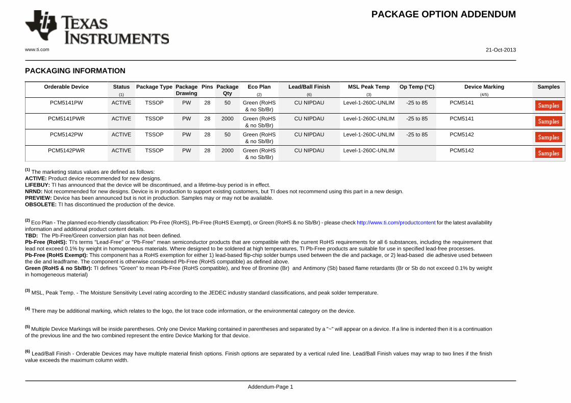
PACKAGE OPTION ADDENDUM
www.ti.com 21-Oct-2013
Addendum-Page 1
PACKAGING INFORMATION
Orderable Device Status(1)
Package Type PackageDrawing
Pins PackageQty
Eco Plan(2)
Lead/Ball Finish(6)
MSL Peak Temp(3)
Op Temp (°C) Device Marking(4/5)
Samples
PCM5141PW ACTIVE TSSOP PW 28 50 Green (RoHS& no Sb/Br)
CU NIPDAU Level-1-260C-UNLIM -25 to 85 PCM5141
PCM5141PWR ACTIVE TSSOP PW 28 2000 Green (RoHS& no Sb/Br)
CU NIPDAU Level-1-260C-UNLIM -25 to 85 PCM5141
PCM5142PW ACTIVE TSSOP PW 28 50 Green (RoHS& no Sb/Br)
CU NIPDAU Level-1-260C-UNLIM -25 to 85 PCM5142
PCM5142PWR ACTIVE TSSOP PW 28 2000 Green (RoHS& no Sb/Br)
CU NIPDAU Level-1-260C-UNLIM PCM5142
(1) The marketing status values are defined as follows:ACTIVE: Product device recommended for new designs.LIFEBUY: TI has announced that the device will be discontinued, and a lifetime-buy period is in effect.NRND: Not recommended for new designs. Device is in production to support existing customers, but TI does not recommend using this part in a new design.PREVIEW: Device has been announced but is not in production. Samples may or may not be available.OBSOLETE: TI has discontinued the production of the device.
(2) Eco Plan - The planned eco-friendly classification: Pb-Free (RoHS), Pb-Free (RoHS Exempt), or Green (RoHS & no Sb/Br) - please check http://www.ti.com/productcontent for the latest availabilityinformation and additional product content details.TBD: The Pb-Free/Green conversion plan has not been defined.Pb-Free (RoHS): TI's terms "Lead-Free" or "Pb-Free" mean semiconductor products that are compatible with the current RoHS requirements for all 6 substances, including the requirement thatlead not exceed 0.1% by weight in homogeneous materials. Where designed to be soldered at high temperatures, TI Pb-Free products are suitable for use in specified lead-free processes.Pb-Free (RoHS Exempt): This component has a RoHS exemption for either 1) lead-based flip-chip solder bumps used between the die and package, or 2) lead-based die adhesive used betweenthe die and leadframe. The component is otherwise considered Pb-Free (RoHS compatible) as defined above.Green (RoHS & no Sb/Br): TI defines "Green" to mean Pb-Free (RoHS compatible), and free of Bromine (Br) and Antimony (Sb) based flame retardants (Br or Sb do not exceed 0.1% by weightin homogeneous material)
(3) MSL, Peak Temp. - The Moisture Sensitivity Level rating according to the JEDEC industry standard classifications, and peak solder temperature.
(4) There may be additional marking, which relates to the logo, the lot trace code information, or the environmental category on the device.
(5) Multiple Device Markings will be inside parentheses. Only one Device Marking contained in parentheses and separated by a "~" will appear on a device. If a line is indented then it is a continuationof the previous line and the two combined represent the entire Device Marking for that device.
(6) Lead/Ball Finish - Orderable Devices may have multiple material finish options. Finish options are separated by a vertical ruled line. Lead/Ball Finish values may wrap to two lines if the finishvalue exceeds the maximum column width.

PACKAGE OPTION ADDENDUM
www.ti.com 21-Oct-2013
Addendum-Page 2
Important Information and Disclaimer:The information provided on this page represents TI's knowledge and belief as of the date that it is provided. TI bases its knowledge and belief on informationprovided by third parties, and makes no representation or warranty as to the accuracy of such information. Efforts are underway to better integrate information from third parties. TI has taken andcontinues to take reasonable steps to provide representative and accurate information but may not have conducted destructive testing or chemical analysis on incoming materials and chemicals.TI and TI suppliers consider certain information to be proprietary, and thus CAS numbers and other limited information may not be available for release.
In no event shall TI's liability arising out of such information exceed the total purchase price of the TI part(s) at issue in this document sold by TI to Customer on an annual basis.

TAPE AND REEL INFORMATION
*All dimensions are nominal
Device PackageType
PackageDrawing
Pins SPQ ReelDiameter
(mm)
ReelWidth
W1 (mm)
A0(mm)
B0(mm)
K0(mm)
P1(mm)
W(mm)
Pin1Quadrant
PCM5141PWR TSSOP PW 28 2000 330.0 16.4 6.9 10.2 1.8 12.0 16.0 Q1
PCM5142PWR TSSOP PW 28 2000 330.0 16.4 6.9 10.2 1.8 12.0 16.0 Q1
PACKAGE MATERIALS INFORMATION
www.ti.com 21-Oct-2013
Pack Materials-Page 1

*All dimensions are nominal
Device Package Type Package Drawing Pins SPQ Length (mm) Width (mm) Height (mm)
PCM5141PWR TSSOP PW 28 2000 367.0 367.0 38.0
PCM5142PWR TSSOP PW 28 2000 367.0 367.0 38.0
PACKAGE MATERIALS INFORMATION
www.ti.com 21-Oct-2013
Pack Materials-Page 2


IMPORTANT NOTICE
Texas Instruments Incorporated and its subsidiaries (TI) reserve the right to make corrections, enhancements, improvements and otherchanges to its semiconductor products and services per JESD46, latest issue, and to discontinue any product or service per JESD48, latestissue. Buyers should obtain the latest relevant information before placing orders and should verify that such information is current andcomplete. All semiconductor products (also referred to herein as “components”) are sold subject to TI’s terms and conditions of salesupplied at the time of order acknowledgment.TI warrants performance of its components to the specifications applicable at the time of sale, in accordance with the warranty in TI’s termsand conditions of sale of semiconductor products. Testing and other quality control techniques are used to the extent TI deems necessaryto support this warranty. Except where mandated by applicable law, testing of all parameters of each component is not necessarilyperformed.TI assumes no liability for applications assistance or the design of Buyers’ products. Buyers are responsible for their products andapplications using TI components. To minimize the risks associated with Buyers’ products and applications, Buyers should provideadequate design and operating safeguards.TI does not warrant or represent that any license, either express or implied, is granted under any patent right, copyright, mask work right, orother intellectual property right relating to any combination, machine, or process in which TI components or services are used. Informationpublished by TI regarding third-party products or services does not constitute a license to use such products or services or a warranty orendorsement thereof. Use of such information may require a license from a third party under the patents or other intellectual property of thethird party, or a license from TI under the patents or other intellectual property of TI.Reproduction of significant portions of TI information in TI data books or data sheets is permissible only if reproduction is without alterationand is accompanied by all associated warranties, conditions, limitations, and notices. TI is not responsible or liable for such altereddocumentation. Information of third parties may be subject to additional restrictions.Resale of TI components or services with statements different from or beyond the parameters stated by TI for that component or servicevoids all express and any implied warranties for the associated TI component or service and is an unfair and deceptive business practice.TI is not responsible or liable for any such statements.Buyer acknowledges and agrees that it is solely responsible for compliance with all legal, regulatory and safety-related requirementsconcerning its products, and any use of TI components in its applications, notwithstanding any applications-related information or supportthat may be provided by TI. Buyer represents and agrees that it has all the necessary expertise to create and implement safeguards whichanticipate dangerous consequences of failures, monitor failures and their consequences, lessen the likelihood of failures that might causeharm and take appropriate remedial actions. Buyer will fully indemnify TI and its representatives against any damages arising out of the useof any TI components in safety-critical applications.In some cases, TI components may be promoted specifically to facilitate safety-related applications. With such components, TI’s goal is tohelp enable customers to design and create their own end-product solutions that meet applicable functional safety standards andrequirements. Nonetheless, such components are subject to these terms.No TI components are authorized for use in FDA Class III (or similar life-critical medical equipment) unless authorized officers of the partieshave executed a special agreement specifically governing such use.Only those TI components which TI has specifically designated as military grade or “enhanced plastic” are designed and intended for use inmilitary/aerospace applications or environments. Buyer acknowledges and agrees that any military or aerospace use of TI componentswhich have not been so designated is solely at the Buyer's risk, and that Buyer is solely responsible for compliance with all legal andregulatory requirements in connection with such use.TI has specifically designated certain components as meeting ISO/TS16949 requirements, mainly for automotive use. In any case of use ofnon-designated products, TI will not be responsible for any failure to meet ISO/TS16949.
Products ApplicationsAudio www.ti.com/audio Automotive and Transportation www.ti.com/automotiveAmplifiers amplifier.ti.com Communications and Telecom www.ti.com/communicationsData Converters dataconverter.ti.com Computers and Peripherals www.ti.com/computersDLP® Products www.dlp.com Consumer Electronics www.ti.com/consumer-appsDSP dsp.ti.com Energy and Lighting www.ti.com/energyClocks and Timers www.ti.com/clocks Industrial www.ti.com/industrialInterface interface.ti.com Medical www.ti.com/medicalLogic logic.ti.com Security www.ti.com/securityPower Mgmt power.ti.com Space, Avionics and Defense www.ti.com/space-avionics-defenseMicrocontrollers microcontroller.ti.com Video and Imaging www.ti.com/videoRFID www.ti-rfid.comOMAP Applications Processors www.ti.com/omap TI E2E Community e2e.ti.comWireless Connectivity www.ti.com/wirelessconnectivity
Mailing Address: Texas Instruments, Post Office Box 655303, Dallas, Texas 75265Copyright © 2016, Texas Instruments Incorporated