rn4870/71 bluetooth low energy module - microchip...
TRANSCRIPT

RN4870/71Bluetooth® Low Energy Module
Features• Qualified for Bluetooth SIG v5.0 Core
Specification • Certified to FCC, ISED, CE, KCC, NCC and
SRRC• On-Board Bluetooth Low Energy (BLE) Stack• ASCII Command Interface API over UART• Scripting Engine for Hostless Operation• Compact Form Factor – The RN4870/71 family
comes in four different sizes from 6 mm x 8 mm to 12 mm x 22 mm:- RN4870: 12 mm x 22 mm- RN4871: 9 mm x 11.5 mm- RN4870U: 12 mm x 15 mm- RN4871U: 6 mm x 8 mm
• Beacon Private Service for Beacon Services• UART Transparent Service for Serial Data
Applications• Remote Configuration Over-the-Air
Operational• Operating Voltage: 1.9V to 3.6V (3.3V typical)• Temperature Range:
- -20°C to +70°C (Normal)- -40°C to +85°C (Industrial)
• Supports UART• Up to Three Pulse Width Modulation (PWM)
Outputs (only for RN4870)
RF/Analog Features• ISM Band 2.402 to 2.480 GHz Operation• Channels: 0-39• RX Sensitivity: -90 dBm• TX Power: 0 dBm• RSSI Monitor
MAC/Baseband/Higher Layer Features• Secure AES128 Encryption• GAP, GATT, SM, L2CAP and Integrated Public
Profiles• Customer Can Create up to Five Public and Four
Private Services• Keyboard I/O Authentication• Software Configurable Role as Peripheral or
Central and Client or Server
Antenna Options• Chip Antenna Range based on Open Air
Measurements and Phone-Module Connection: - RN4870: Up to 50 m - RN4871: Up to 10 m
• External Antenna Connection via RF Pad (RN4870U/RN4871U)
Applications• Health/Medical Devices• Sports Activity/Fitness Meters• Beacon Applications• Internet of Things (IoT) Sensor Tag• Remote Control • Wearable Smart Devices and Accessories• Smart Energy/Smart Home• Industrial Control
2016-2019 Microchip Technology Inc. DS50002489D-page 1

RN4870/71
Table of Contents1.0 Device Overview .......................................................................................................................................................................... 32.0 Specifications ..............................................................................................................................................................................113.0 Interface PINs............................................................................................................................................................................. 134.0 Physical Dimensions And Attributes ........................................................................................................................................... 155.0 Application Reference Circuits ................................................................................................................................................... 256.0 ASCII Command API .................................................................................................................................................................. 297.0 Supported Services .................................................................................................................................................................... 318.0 Antenna Characteristics ............................................................................................................................................................. 339.0 Timing Characteristics ................................................................................................................................................................ 3510.0 Regulatory Approval ................................................................................................................................................................... 3711.0 Ordering Information .................................................................................................................................................................. 45The Microchip WebSite ........................................................................................................................................................................ 47Customer Change Notification Service ................................................................................................................................................ 47Customer Support ................................................................................................................................................................................ 47Product Identification System............................................................................................................................................................... 49TO OUR VALUED CUSTOMERSIt is our intention to provide our valued customers with the best documentation possible to ensure successful use of your Microchip products. To this end, we will continue to improve our publications to better suit your needs. Our publications will be refined and enhanced as new volumes and updates are introduced. If you have any questions or comments regarding this publication, please contact the Marketing Communications Department via E-mail at [email protected]. We welcome your feedback.
Most Current Data SheetTo obtain the most up-to-date version of this data sheet, please register at our Worldwide Web site at:
http://www.microchip.comYou can determine the version of a data sheet by examining its literature number found on the bottom outside corner of any page. The last character of the literature number is the version number, (e.g., DS30000000A is version A of document DS30000000).
ErrataAn errata sheet, describing minor operational differences from the data sheet and recommended workarounds, may exist for current devices. As device/documentation issues become known to us, we will publish an errata sheet. The errata will specify the revision of silicon and revision of document to which it applies.To determine if an errata sheet exists for a particular device, please check with one of the following:• Microchip’s Worldwide Web site; http://www.microchip.com• Your local Microchip sales office (see last page)When contacting a sales office, please specify which device, revision of silicon and data sheet (include literature number) you are using.
Customer Notification SystemRegister on our web site at www.microchip.com to receive the most current information on all of our products.
DS50002489D-page 2 2016-2019 Microchip Technology Inc.

RN4870/71
1.0 DEVICE OVERVIEW1.1 OverviewThe RN4870/71 BLE module integrates Bluetooth 5.0baseband controller, on-board Bluetooth stack, digital and analog I/O, and RF power amplifier into one solution.
Table 1-1 shows the various options for packaging and features available in the RN4870/71 family. Table 1-2 provides the description of the pin functions for all the modules in the RN4870/71 family. Figure 1-1 through Figure 1-4 show the pinout for the different modules.
TABLE 1-1: RN4870/71 FAMILY
Part Number(1) Antenna On-Board Shielding Number of
Pins Dimensions Operating Temperature Range
RN4870-V/RMXXX Yes Yes 33 12 mm x 22 mm -20°C to +70°CRN4870U-V/RMXXX No No 30 12 mm x 15 mm -20°C to +70°CRN4871-V/RMXXX Yes Yes 16 9 mm x 11.5 mm -20°C to +70°CRN4871U-V/RMXXX No No 17 6 mm x 8 mm -20°C to +70°CRN4870-I/RMXXX Yes Yes 33 12 mm x 22 mm -40°C to +85°CRN4871-I/RMXXX Yes Yes 16 9 mm x 11.5 mm -40°C to +85°C
Note 1: The last three digits in P/N indicate the firmware version. At the time of publication, the latest firmware version is 1.28. Ensure to check product webpage for latest part number and firmware version.
TABLE 1-2: PIN DESCRIPTION RN4870U RN4870 RN4871U RN4871 Name Type Description
— 1 — — GND Power Ground reference— 2 — — GND Power Ground reference1 3 12 13 GND Power Ground reference2 4 11 14 VBAT Power Positive supply input. Range: 1.9V~3.6V— — 10 — BK_IN Power Buck power supply input
Can be connected to the VBAT pinConnect to 10 µF low ESR ceramic capacitorVoltage range: 1.9V to 3.6V
3 5 — — P2_2 D I/O GPIOPWM1 (only for RN4870) Default: Input; pulled-high
4 6 — — VDD_IO Power VDD; power inputSame input pin as VBATCan be connected to the VBAT pin
5 7 — — VDD_IO Power VDD; power inputSame input pin as VBATCan be connected to the VBAT pin
6 8 — — ULPC_O Power 1.2V ULPC LDO outputUsed for diagnostic purposesDo not connect to any pin or deviceFor measurement, connect a bypass 1 µFcapacitor to ground
7 9 — — P2_3 D I/O GPIOPWM2 (only for RN4870) Default: Input; pulled-high
8 10 — — BK_O Power 1.55V Buck power supply output for diagnostic purposeDo not connect
2016-2019 Microchip Technology Inc. DS50002489D-page 3

RN4870/71
— — 13 6 P1_6 D Configurable pin. Refer to Section 1.2 “Module Configuration” for details. When connected to host MCU, set the pin connected to pin P1_6 in either high impedance or drive pin low during firmware start-up (approximately 22 msec).
— — 14 5 P1_7 D Configurable pin. Refer to Section 1.2 “Module Configuration” for details.
9 11 15 15 P2_7 D O/p UART_TX_IND output pin. Provides indication if RN4870 is transmitting to host MCU over UART. Pulled low before UART TX begins and pulled high after UART TX is over.
10 12 — — P1_1 D I/OA I/p
GPIO; default: Input; pulled-high AD9Configured as the BLEDK_STATUS1_IND pin by default
11 13 2 3 P1_2 D I/OA I/p
GPIO; default: Input; pulled-highAD10; I2C SCL pin
12 14 3 4 P1_3 D I/O GPIO; default: Input; pulled-highAD11; I2C SDA pin
13 15 8 11 P0_0 D I/O GPIO; default: Input; pulled-highAD0Configured as the UART_CTS pin by default
14 16 — — P1_0 D I/O GPIO; default: Input; pulled-highAD8Configured as the BLEDK_STATUS2_IND pin by default
15 17 6 9 P3_6 D I/O GPIO; default: Input; pulled-high(only for RN4870) Configured as the UART_RTS pin by default
16 18 16 16 P2_0 D I/p System configuration input; 1: Application mode0: Test mode/Flash update/EEPROM configurationDefault: Input; pulled-high
17 19 — — P2_4 D I/O GPIO; default: Input; pulled-high18 20 — — NC — No Connection19 21 7 10 RST_N D I/p Module Reset; active-low; Internally pulled-high20 22 5 7 UART_RX D I/p UART Data input21 23 4 8 UART_TX D O/p UART Data output22 24 — — P3_1 D I/O GPIO; default: Input; pulled-high
Configured as RSSI_IND pin by default; SPI NCS Bus
23 25 — — P3_2 D I/p GPIO; default: Input; pulled-highConfigured as the LINK_DROP pin by default; SPI MISO pin
24 26 — — P3_3 D I/p GPIO; default: Input; pulled-highConfigured as the UART RX Indication pin by default; SPI MOSI pin
25 27 — — P3_4 D I/p GPIO; default: Input; pulled-highConfigured as the PAIRING_KEY pin by default; SPI SCLK pin
TABLE 1-2: PIN DESCRIPTION (CONTINUED)RN4870U RN4870 RN4871U RN4871 Name Type Description
DS50002489D-page 4 2016-2019 Microchip Technology Inc.

RN4870/71
FIGURE 1-1: PIN DIAGRAM - RN4870U
26 28 — — P3_5 D I/OA I/p
GPIO; default: Input; pulled-highLED1; provides indication whether the module is ON/OFF
27 29 — — P0_7 D I/O GPIO; default: Input; pulled-highConfigured to the LOW_BATTERY_INDICATOR pin by default
28 30 9 12 P0_2 D I/O AD2LED0: Provides indication whether the module is in ON/OFF mode
29 31 17 2 GND Power Ground Reference— 32 — — GND Power Ground Reference30 — 1 — BT_RF A I/O External Antenna connection (50 ohms). Only for
RN4870U and RN4871U. No connection for RN4871.— 33 — — GND Power Ground Reference
Legend: Pin Type Abbreviations: A = Analog D = Digital I/O = Input/Output I/p = Input O/p = Output
TABLE 1-2: PIN DESCRIPTION (CONTINUED)RN4870U RN4870 RN4871U RN4871 Name Type Description
TP-2 TP-2 CLDO_O
TP-1 VCC_PATP-3 VCC_RF
TP-1TP-3GND
GNDVBATP2_2
VDD_IOVDD_IO
ULPC_OP2_3
BK_OP2_7/TX_IND
P1_1P1_2P1_3
P0_0
/CTS
P1_0
P3_6
/RTS
P2_0
/MO
DE
P2_4 NC
RST
_N
P0_2/LEDP0_7P3_5P3_4P3_3P3_2P3_1UART_TXUART_RX
3456789
101112
13 14 15 16 17 18 19
20212223242526272829
301 BT_RF2
30 1
Top View Bottom View
2016-2019 Microchip Technology Inc. DS50002489D-page 5

RN4870/71
FIGURE 1-2: PIN DIAGRAM - RN4870FIGURE 1-3: PIN DIAGRAM - RN4871U
TP-2 TP-2 CLDO_O
TP-1 VCC_PATP-3 VCC_RF
TP-1TP-3
GNDGND
GNDGND
GND
GNDVBATP2_2
VDD_IOVDD_IO
ULPC_OP2_3
BK_OP2_7/TX_IND
P1_1P1_2P1_3
P0_0
/CTS
P1_0
P3_6
/RTS
P2_0
/MO
DE
P2_4 NC
RST
_N
P0_2/LEDP0_7P3_5P3_4P3_3P3_2P3_1UART_TXUART_RX
13312
3456789
1011121314
15 16 17 18 19 20 21
22232425262728293031
3233
Top View Bottom View
34 12
56789
1310 11 12
141516
17 17
1
TP-1
TP-2
TP-3
TP-4
TP-5
VBAT
BK_
IN
GN
DP1
_6
P1_7P2_7P2_0
GND
BT_
RF
P1_2
P1_3
UAR
T_TX
UART_RX
RST_NP3_6
P0_2P0_0
TP-1 CLDO_O
VCC_PA TP-3 VCC_RF TP-2 TP-4 ULPC_O
TP-5 BK_O
Top View Bottom View
DS50002489D-page 6 2016-2019 Microchip Technology Inc.

RN4870/71
FIGURE 1-4: PIN DIAGRAM - RN487116
TP-5
TP-2
TP-3
TP-4TP-1
2016-2019 Microchip Technology Inc. DS50002489D-page 7

RN4870/71
1.2 Module ConfigurationThe GPIO pins of the RN4870 and RN4871 modules can be configured to different functions using the ASCII command interface. Table 1-3 shows the various pins in the RN4870/71 module that are available for configuration and their default configuration settings. Table 1-4 provides details on each available function.Table 1-5 shows the status of the module as indicated by the Status 1 and Status 2 indication pins. Table 1-6 shows the details of test pads that are present on the bottom side of the module, used for diagnostic purposes during testing. Figure 1-5 shows all the key elements of the module.
TABLE 1-3: CONFIGURABLE PINS AND DEFAULT FUNCTIONS IN THE RN4870 AND RN4871
Pin NameAvailable in
Default FunctionRN4870 RN4871
P0_7 x — Low Battery IndicationP1_0 x — Status 2P1_1 x — Status 1P2_2 x — NoneP2_4 x — NoneP3_1 x — RSSI IndicationP3_2 x — Link DropP3_3 x — UART RX IndicationP3_4 x — Pairing KeyP3_5 x — NoneP1_2 x x NoneP1_3 x x NoneP1_6 — x UART RX IndicationP1_7 — x None
TABLE 1-4: CONFIGURABLE FUNCTIONS AND DESCRIPTIONS Function Name Description
Low Battery Indication Pin output goes low when the VDD is below a specified level. To set the threshold level, change the EEPROM settings.
Status 1 Use this indication pin along with the Status 2 pin to indicate the current status of the module. Refer to Table 1-5 for details of the status indication.
Status 2 Use this indication pin along with the Status 1 pin to indicate the current status of the module. Refer to Table 1-5 for details of the status indication.
RSSI Indication Use this indication pin to indicate the quality of the link based on the RSSI level. If the RSSI level is lower than the specified threshold value, then the RSSI indication pin goes low. Set the threshold for the RSSI link quality in EEPROM.
Link Drop When the RN4870/71 is connected to a remote device, the host MCU can use the Link Drop pin to force the module to disconnect the link and enter Shutdown state. The pin needs to be pulled low for at least 10 ms.
UART RX Indication Use this pin to enable communication with the UART when the module is in Low-Power mode. When not in Low-Power mode, the module runs on a 16 MHz clock. If Low-Power mode is enabled on the module by using command SO,1, the module runs on a 32 kHz clock thus reducing power consumption. However, in Low-Power mode, the host MCU cannot communicate with the module via the UART since the UART is not operational. If the user intends to provide data or commands via UART in the Low-Power mode, then the UART RX INDICATION pin must be pulled low and the user needs to wait for at least five milliseconds before sending the data. Pulling the UART RX INDICATION pin low allows the module to operate the 16 MHz clock and to enable UART.
DS50002489D-page 8 2016-2019 Microchip Technology Inc.

RN4870/71
FIGURE 1-5: BLOCK DIAGRAM OF THE RN4870/71
Pairing Key When the RN4870/71 is connected to a remote device, the host MCU can use the Pairing Key pin to force the module to disconnect the link and go back to Standby state. The pin must be pulled down for at least 160 ms.
RF Active Indication Use this indication pin to indicate that the module is currently performing an active transmission and receiving BLE data.
TABLE 1-5: STATUS INDICATION PINS Status 1 Status 2 State
High High Power OnHigh Low Standby stateLow Low Connection establishedLow High Data session open (Transparent UART)
TABLE 1-6: TEST POINTS ON THE BOTTOM SIDE RN4870U RN4870 RN4871U RN4871 Symbol Description
TP-1 TP-1 TP-3 TP-3 VCC_PA 1.55V RF PA LDOTP-2 TP-2 TP-1 TP-5 CLDO_O 1.2V CLDO OutputTP-3 TP-3 TP-2 TP-2 VCC_RF 1.2V RF LDO Output
— — TP-4 TP-4 ULPC_O 1.2V ULPC LDO Output— — TP-5 TP-1 BK_O 1.55V Buck Reg Output
TABLE 1-4: CONFIGURABLE FUNCTIONS AND DESCRIPTIONS (CONTINUED)Function Name Description
RN4870/RN4871
2016-2019 Microchip Technology Inc. DS50002489D-page 9

RN4870/71
NOTES:DS50002489D-page 10 2016-2019 Microchip Technology Inc.

RN4870/71
2.0 SPECIFICATIONSTable 2-1 provides the general specifications for the module. Table 2-2, Table 2-3 and Table 2-4 provide the electrical characteristics and the current consumption of the module.TABLE 2-1: GENERAL SPECIFICATIONSSpecification Description
Standard Compliance Bluetooth 5.0 Frequency Band 2.402 to 2.480 GHzModulation Method GFSKMaximum Data Rate (Transparent UART) 10 kbps (iOS®9)Antenna CeramicInterface UART, AIO, PIOOperating Range 1.9V to 3.6VSensitivity -90 dBm RF TX Power 0 dBmOperating Temperature Range for RN4870-I and RN4871-I modules -40°C to +85°COperating Temperature Range for RN4870-V and RN4871-V modules -20°C to +70°CStorage Temperature Range -40°C to +125°COperating Relative Humidity Range 10% to 90%Storage Relative Humidity Range 10% to 90%Moisture Sensitivity Level 2
TABLE 2-2: ELECTRICAL CHARACTERISTICSParameter Min. Typ. Max. Units
Supply Voltage (VDD) 1.9 — 3.6 VI/O Voltage LevelsVIL Input Logic Levels Low VSS — 0.3 VDD VVIH Input Logic Levels High 0.7 VDD — VDD VVOL Output Logic Levels Low Vss — 0.2 VDD VVOH Output Logic Levels High 0.8 VDD — VDD VResetReset Low Duration 63 — — nsInput and Tri-State Current withPull-Up Resistance 34 48 74 kPull-Down Resistance 29 47 86 k
2016-2019 Microchip Technology Inc. DS50002489D-page 11

RN4870/71
TABLE 2-3: CURRENT CONSUMPTIONParameter Min. Typ. Max. Units
Supply CurrentTX mode Peak Current at VDD = 3V, TX = 0 dBm, Buck mode — 10 at +25°C 13 at +75°C/+85°C mARX mode Peak Current at VDD = 3V, Buck mode — 10 at +25°C 13 at +75°C/+85°C mALow-Power Mode Current(2) — 60 at +25°C — µAShutdown Low-Power Mode 1 — 2.9 µANote 1: The current measurements are characterized across a sample of the RN4870/71 module at room tem-
perature (+25°C), unless otherwise noted.2: For more details on Low-Power mode, refer to the “RN4870/71 Bluetooth® Low Energy Module User’s
Guide” (DS50002466).
TABLE 2-4: CURRENT CONSUMPTION DURING APPLICATION MODE
Test Mode Interval(ms) Average Current Consumption
Advertising(1,2,3)
20 1.061 mA50 505 µA
100 298 µA500 113 µA
1000 89 µA
Connected(1,2,4)
18.75 2.23 mA50 2.13 mA
100 2.10 mA500 83 µA
1000 80 µANote 1: These measurements are done at an operating temperature of +25°C at 3.3V and are characterized
across a sample of the RN4870/71 module.2: Measurements taken with version 1.18 firmware loaded onto the module.3: The advertising packet data payload is approximately 15 bytes in length.4: The amount of data being transmitted between two peer devices can affect the average current measured.
The average current measurements are done with only the necessary Bluetooth packets being exchanged to keep the connection active at the stated interval.
DS50002489D-page 12 2016-2019 Microchip Technology Inc.

RN4870/71
3.0 INTERFACE PINSFigure 3-1 shows the power scheme using a 3.3V low-dropout regulator to the RN487x and a host MCU. This scheme ensures that the same voltage is used for both the module and the MCU.Figure 3-1 also shows the basic UART connections to the host MCU.Figure 3-2 shows the recommended connections for running the RN4870/71 on coin cell battery.
FIGURE 3-1: POWER SCHEME
System Configurator
System Configurator
Note 1: Ensure VDD_IO and MCU VDD voltages are compatible2: Control and Indication ports are configurable3: To implement low-power operation, enable the UART_RX_IND
pin and connect to ground.
Note 1: Ensure VDD_IO and MCU VDD voltages are compatible2: Control and Indication ports are configurable3: 10 µF (X5R) and 330 ohm resistor are required for RN487x4: BK_IN connects to VBAT for RN4871U5: To implement low-power operation, enable the UART_RX_IND
pin and connect to ground.
RN4870/71/70U
RN4871U
Reset IC Reset
System Configurator
System Configurator
Note 1: Ensure VDD_IO and MCU VDD voltages are compatible2: Control and Indication ports are configurable3: To implement low-power operation, enable the UART_RX_IND
pin and connect to ground.
Note 1: Ensure VDD_IO and MCU VDD voltages are compatible2: Control and Indication ports are configurable3: 10 µF (X5R) and 330 ohm resistor are required for RN487x4: BK_IN connects to VBAT for RN4871U5: To implement low-power operation, enable the UART_RX_IND
pin and connect to ground.
RN4870/71/70U
RN4871U
Reset IC Reset
Reset IC Reset
2016-2019 Microchip Technology Inc. DS50002489D-page 13

RN4870/71
FIGURE 3-2: RN4870/71 COIN CELL POWER SCHEMEThe Configuration pins on the RN4870 can also be configured through Windows®-based User Interface (UI) Configuration tool, BLEDK3.
RN4870/71
Note 1: Application includes ADC, PWM (RN4870), and I2C bus interface
2: BK_IN connection is needed only for RN4871U.3: To implement low-power operation, enable the
UART_RX_IND pin and connect to ground.
Reset IC Reset
DS50002489D-page 14 2016-2019 Microchip Technology Inc.

RN4870/71
4.0 PHYSICAL DIMENSIONS ANDATTRIBUTES
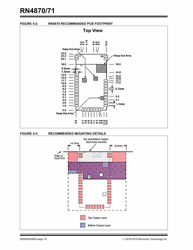
4.1 RN4870 ModuleFigure 4-1 shows the physical dimensions of the RN4870 module. Figure 4-2 illustrates the recommended PCB layout, and Figure 4-3 shows the recommended mounting details.Ensure that there is no top copper layer near the test pin area, indicated by the shaded keep out areas, as shown in Figure 4-2. When laying out the host PCB, the
areas under the antenna must not contain any top, inner layer, or bottom copper as shown in Figure 4-3. A low-impedance ground plane ensures the best radio performance (best range, lowest noise). Figure 4-3 also shows a minimum ground plane area to the left and right side of the module for best antenna performance. The ground plane can be extended beyond the minimum recommended as required for host PCB EMC noise reduction. For best range performance, keep all external metal at least 30 mm away from the ceramic chip antenna.
FIGURE 4-1: RN4870 MODULE DIMENSIONS
2016-2019 Microchip Technology Inc. DS50002489D-page 15
RN4870/71
FIGURE 4-2: RN4870 RECOMMENDED PCB FOOTPRINTFIGURE 4-3: RECOMMENDED MOUNTING DETAILS
DS50002489D-page 16 2016-2019 Microchip Technology Inc.

RN4870/71
4.2 RN4870U ModuleFigure 4-4 shows the physical dimensions of the RN4870U module. Figure 4-5 illustrates the recommended PCB layout, and Figure 4-6 shows the recommended mounting details. A low-impedance ground plane ensures the best radio performance (best range, lowest noise). Pin 30 (BT_RF) is a 50 ohm connection that can be connectedto an external antenna such as a PCB trace antenna, a component (chip) antenna, or through a host PCB 50 ohm microstrip trace. This trace can be extended to include passive parts for antenna attenuation padding, impedance matching, or to provide test posts. It is recommended that the microstrip trace be as short as possible for minimum loss and best impedance matching. If the microstrip trace is longer, a 50 ohm impedance is recommended.
FIGURE 4-4: RN4870U MODULE DIMENSIONS
2016-2019 Microchip Technology Inc. DS50002489D-page 17

RN4870/71
FIGURE 4-5: RN4870U RECOMMENDED PCB FOOTPRINTFIGURE 4-6: RN4870U RECOMMENDED PCB MOUNTING
DS50002489D-page 18 2016-2019 Microchip Technology Inc.

RN4870/71
4.3 RN4871 ModuleFigure 4-7 shows the physical dimensions of the RN4871 module. Figure 4-8 illustrates the recommended PCB layout, and Figure 4-9 shows the recommended mounting details.Ensure that there is no top copper layer near the test pin area, indicated by the shaded keep out areas, as shown in Figure 4-8. When laying out the host PCB, the areas under the antenna must not contain any top,inner layer, or bottom copper as shown in Figure 4-9. A low-impedance ground plane ensures the best radio performance (best range, lowest noise). Figure 4-9 also shows a space area around the antenna section for best antenna performance. The ground plane can be extended beyond the minimum recommended as required for host PCB EMC noise reduction. For best range performance, keep all external metal at least 30 mm away from the ceramic chip antenna.
FIGURE 4-7: RN4871 MODULE DIMENSIONS
1.5
1
2.7
5.1
7.5
6.3
9.0
2.1
0.6
0.0
9.0
7.5
16
6.3
5.1
1.0
3.9
1.5
0.0
0.0
4.11
0.58
8.31
6.93
5.25
5.33
5.79
0.63
0.0
0.0
3.1
1.9
4.3
6.7
3.9
16
0.700.00
7.18
11.14
0.7
0.0
3.1
1.9
4.3
6.7
0.5
2.7
TP-5
TP-2
TP-3
1.2 2.38
4.85
6.01
0.7
TP-5
TP-2
TP-3
4.75
6.77.5
5.5
11.5
9.54
7.5
5.5
11.5
TP-4 3.68
6.0
0.0
TP-4
Shieldmountinghole
Shieldmounting hole
Pad Positions Test Point Positions
Bottom View
Pad Detail
TP-1TP-1
Shieldmounting hole
Dimensions are in millimetersTolerances:PCB : +/-0.06mm
Top View Side View
2016-2019 Microchip Technology Inc. DS50002489D-page 19

RN4870/71
FIGURE 4-8: RN4871 RECOMMENDED PCB FOOTPRINTFIGURE 4-9: RN4871 RECOMMENDED PCB MOUNTING SUGGESTION
1.2
0.5
1.5
1.0
2.7
3.0
5.1
4.3
7.5
6.3
9.0
1.5
0.7
0.0
1.9
3.1
4.34.6
6.7
Keep Out Area
1.5Keep Out Area
7.00.
0
5.5
7.5
11.5
3.9
8.0
Dimensions are in millimeters
Top View
DS50002489D-page 20 2016-2019 Microchip Technology Inc.

RN4870/71
4.4 RN4871U ModuleFigure 4-10 shows the physical dimensions of the RN4871U module. Figure 4-11 illustrates the recom-mended PCB layout. It is highly recommended to layout the host PCB as suggested in Figure 4-12. Figure 4-13 shows the recommended placement for the module on the host PCB board. For optimal transmission and reception sensitivity, place the module at the edge of the board.A low-impedance ground plane ensures the best radio performance (best range, lowest noise). Pin 1 (BT_RF) is a 50 ohm connection that can be connected to an external antenna such as a PCB trace antenna, a component (chip) antenna, or through a host PCB 50 ohm microstrip trace. This trace can be extended to include passive parts for antenna attenuation padding, impedance matching, or to provide test posts. It is recommended that the microstrip trace to be as short as possible for minimum loss and best impedance matching. If the microstrip trace is longer, a 50 ohm impedance is recommended.
FIGURE 4-10: RN4871U MODULE DIMENSIONS
Top View Bottom ViewSide View
2016-2019 Microchip Technology Inc. DS50002489D-page 21

RN4870/71
FIGURE 4-11: RN4871U RECOMMENDED PCB FOOTPRINTFIGURE 4-12: RN4871U RECOMMENDED PCB MOUNTING
DS50002489D-page 22 2016-2019 Microchip Technology Inc.

RN4870/71
FIGURE 4-13: RECOMMENDATIONS FOR THE PLACEMENT OF THE MODULE ON THE HOSTPCB BOARD
4.5 Soldering RecommendationsThe RN4870/71 Bluetooth module is assembled using standard lead-free reflow profile IPC/JEDEC J-STD-020. The module can be soldered to the host PCB using standard leaded and lead-free solder reflow profiles. To avoid damaging the module, the following recom-mendations are given:• Microchip Technology Application Note, “AN233
Solder Reflow Recommendation” (DS00233) provides solder reflow recommendations
• Do not exceed peak temperature (TP) of 250°C• Refer to the solder paste data sheet for specific
reflow profile recommendations• Use no-clean flux solder paste• Do not wash as moisture can be trapped under
the shield• Use only one flow. If the PCB requires multiple
flows, apply the module on the final flow.
Acceptable
Best
Acceptable
Lowestperformance
2016-2019 Microchip Technology Inc. DS50002489D-page 23

RN4870/71
NOTES:DS50002489D-page 24 2016-2019 Microchip Technology Inc.

RN4870/71
5.0 APPLICATION REFERENCECIRCUITS
5.1 External Configuration and Programming
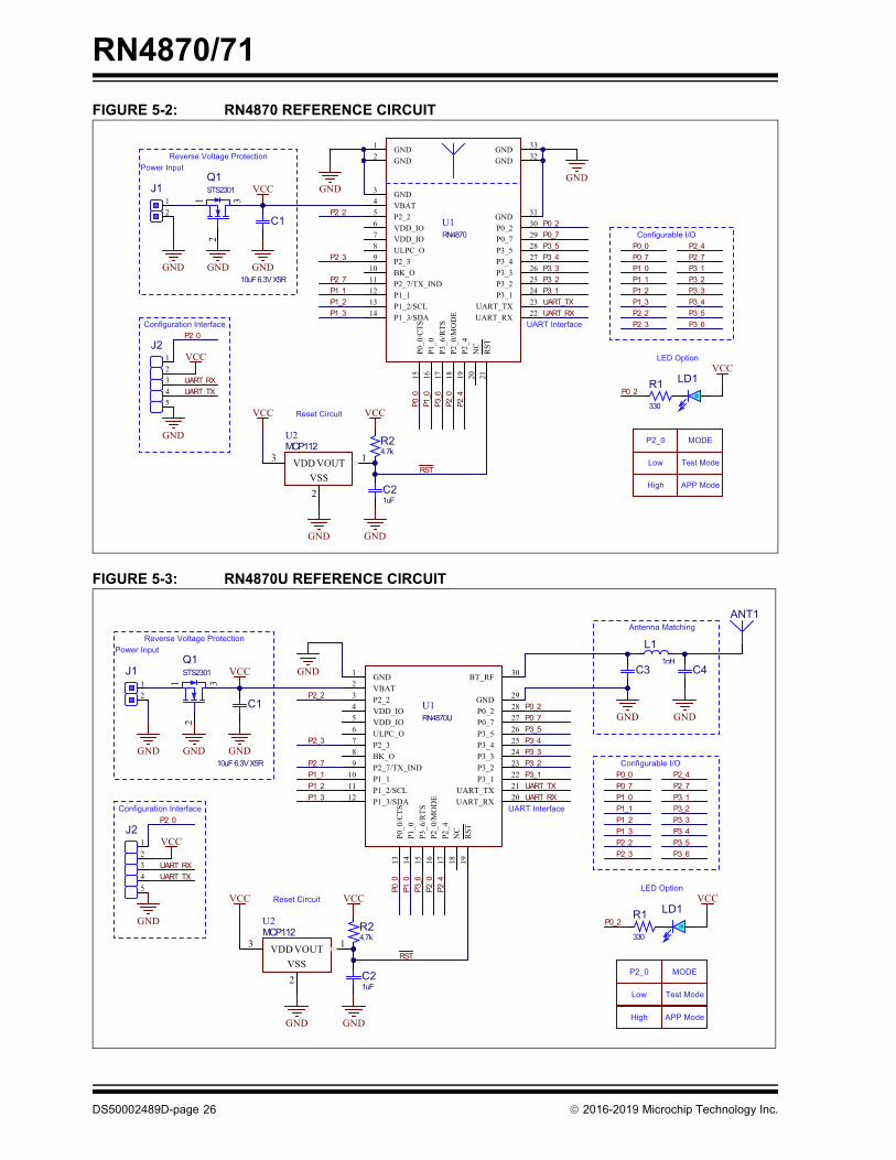
The RN4870/71 module can be configured and firm-ware programmed using an external configuration and programming tool. Figure 5-1 shows the mandatory connections required between the module and the external programming header. It is recommended to include these pin connections on the host PCB for development. For accessing the various configuration and indication pins, use Table 1-2, Table 1-3, Table 1-4 and Table 1-5.
5.2 Reference CircuitFigure 5-2 through Figure 5-5 show the reference circuits for various modules under the RN4870/71 fam-ily. In the circuits, the power input range is 1.9V ~ 3.6V. A battery reverse protection circuit is recommended in case a battery power input is used. Note that the VDD_IO is the same as the power input. In case of a LED connection, the power input must be greater than 3.0V. For the RN4870U, an RF antenna matching circuit must also be included as shown in Figure 5-3.
FIGURE 5-1: EXTERNAL PROGRAMMING HEADER CONFIGURATIONS
RN4870/71
1 P2_0 P2_0
VBAT
1 RXD
1 TXD
1 GND
RXD
TXD
GND
1 VBAT
2016-2019 Microchip Technology Inc. DS50002489D-page 25
RN4870/71
FIGURE 5-2: RN4870 REFERENCE CIRCUITFIGURE 5-3: RN4870U REFERENCE CIRCUIT
RN4870
GND1
GND2
GND3
VBAT4
P2_25
VDD_IO6
VDD_IO7
ULPC_O8
P2_39
BK_O10
P2_7/TX_IND11
P1_112
P1_2/SCL13
P1_3/SDA14
P0_0/CTS
15
P1_0
16
P3_6/RTS
17
P2_0/MODE
18
P2_4
19
NC
20
RST
21
UART_RX22
UART_TX23
P3_124
P3_225
P3_326
P3_427
P3_528
P0_729
P0_230
GND31
GND32
GND33
U1
B
LD1
GNDGND
330
R1
GND
VCC
VCC
UART_TXUART_RX
P0_2
P0_0
P1_0
P1_1P1_2P1_3
P0_7
P2_0
P2_2
P2_3
P2_4
P2_7P3_1P3_2P3_3P3_4P3_5
P3_6
P0_7P3_1P3_2P3_3P3_4P3_5
3
2
1STS2301Q1
P0_0
P1_0
P2_0
P2_4
P3_6
P1_1P1_2P1_3
P2_3
P2_7
P2_2
Configurable I/O
1
2
J1
GND
1
2
3
4
5
J2
GND
Power InputReverse Voltage Protection
Configuration Interface
VCC
UART_TXUART_RX
UART Interface
LED Option
P0_2
10uF 6.3V X5R
C1
GND
4.7kR2
VCC
1uFC2
GND
RSTVDD
3VOUT
1
VSS
2
MCP112U2
GND
VCC Reset Circuit
P2_0 MODE
Low
High
Test Mode
APP Mode
GND1
VBAT2
P2_23
VDD_IO4
VDD_IO5
ULPC_O6
P2_37
BK_O8
P2_7/TX_IND9
P1_110
P1_2/SCL11
P1_3/SDA12
P0_0/CTS
13
P1_0
14
P3_6/RTS
15
P2_0/MODE
16
P2_4
17
NC
18
RST
19
UART_RX20
UART_TX21
P3_122
P3_223
P3_324
P3_425
P3_526
P0_727
P0_228
GND29
BT_RF30
RN4870UU1
B
LD1
GND
GND
330
R1
GND
VCC
VCC
UART_TXUART_RX
P0_2
P0_0
P1_0
P1_1P1_2P1_3
P0_7
P2_0
P2_2
P2_3
P2_4
P2_7P3_1P3_2P3_3P3_4P3_5
P3_6
4.7kR2
VCC
P0_7P3_1P3_2P3_3P3_4P3_5
3
2
1
STS2301Q1
P0_0
P1_0
P2_0
P2_4
P3_6
P1_1P1_2P1_3
P2_3
P2_7
P2_2
Configurable I/O
P2_0 MODE
Low
High
Test Mode
APP Mode
1
2
J1
GND
1
2
3
4
5
J2
GND
Power InputReverse Voltage Protection
Configuration Interface
VCC
UART_TXUART_RX
UART Interface
LED Option
P0_2
C3 C4
ANT1
1nH
L1
10uF 6.3V X5R
C1
GND
1uFC2
GND
GND
Antenna Matching
RSTVDD
3VOUT
1
VSS
2
MCP112U2
GND
VCC Reset Circuit
DS50002489D-page 26 2016-2019 Microchip Technology Inc.

RN4870/71
FIGURE 5-4: RN4871 REFERENCE CIRCUITFIGURE 5-5: RN4871U REFERENCE CIRCUIT
5.3 Power Drop ProtectionTo prevent any problems that may arise when the power supply goes below 1.9V, a power-supply drop-protection circuit is recommended. Essentially, this circuit consists of a Reset IC which acts as an Open Drain with a Delay =< 10 ms, and is triggered at 1.8V
power supply. Figure 5-6 shows a recommended power drop protection circuit.
RN4871
VBAT14
P2_715
P1_6
6
P1_23
P1_34
P0_0
11
P3_6
9
P2_016
RST
10
UART_RX
7
UART_TX
8
P0_212
GND13
NC1
P1_75
GND2
U1
B
LD1
GND
330
R1
GND
VCC
VCC
UART
_TX
UART
_RX
P0_2P1_2P1_3
P1_7
P2_7
4.7kR2
VCC
P0_2
3
2
1
STS2301Q1
P0_0
P2_0
P1_6P3_6
P1_2P1_3
P2_7P2_0
Configurable I/O
P2_0 MODE
Low
High
Test Mode
APP Mode
1
2
J1
GND
1
2
3
4
5
J2
GND
Power Input
Reverse Voltage ProtectionConfiguration Interface
VCC
UART_TXUART_RX
UART Interface
LED Option
P0_2
10uF 6.3V X5R
C1
GNDGND
P0_0
P2_0
P3_6
P1_6
P1_7 1uFC2
GND
RST
Reset Circuit
VDD3
VOUT1
VSS
2
MCP112U2
GND
VCC
RN4871UVBAT
11BK_I
10
P2_7
15
P1_613
P1_22
P1_33
P0_0
8
P3_6
6P2_0
16
RST
7
UART_RX
5
UART_TX4
P0_2
9
GND
17
BT_RF1
P1_7
14
GND12
U1
B
LD1
GND
330
R1
GND
VCC
VCC
UART_TXUART_RX
P0_2
P1_2P1_3
P1_7
P2_7
4.7kR2
VCC
P0_2
3
2
1
STS2301Q1
P0_0
P2_0
P1_6P3_6
P1_2P1_3
P2_7P2_0
Configurable I/O
P2_0 MODE
Low
High
Test Mode
APP Mode
1
2
J1
GND
1
2
3
4
5
J2
GND
Power InputReverse Voltage Protection
Configuration Interface
VCC
UART_TXUART_RX
UART Interface
LED Option
P0_2
10uF 6.3V X5R
C1
GND
P0_0
P2_0
P3_6
P1_6
P1_7
GND
1uFC2
GND
GND
C3 C4
ANT1
1nH
L1
GND
Antenna Matching
RST
VDD3
VOUT1
VSS
2MCP112U2
GND
VCC Reset Circuit
2016-2019 Microchip Technology Inc. DS50002489D-page 27

RN4870/71
FIGURE 5-6: POWER DROP PROTECTION CIRCUITRN4870/71
VBAT
RST_N
Reset IC
OUT VDD
DS50002489D-page 28 2016-2019 Microchip Technology Inc.

RN4870/71
6.0 ASCII COMMAND APIThe RN4870/71 command Application Programming Interfaces (APIs) are documented in the “RN4870/71 Bluetooth® Low Energy Module User's Guide”(DS50002466). The following are the available command options and their categories:• Connection- Establish connection - Disconnect- Bond/Unbond current connection- Start/Stop scan for other devices- Add/Delete peer devices to white list- Read RSSI values- Stop connection process
• I/O- Read/Write I2C- Change settings in the EEPROM- Configure pin functions- Configure GPIO mask- Set/Get GPIO states- Read and write analog data- PWM control (only for RN4870)
• System- Reboot- Factory default- Enter and Exit Command mode- Enter Low-Power mode
• Scripting- Enter Script mode- Declare event handler- Execute current script- List current script- Clear script- Define user function
• GATT Services- Create/Delete public services/characteristics- Read/Write characteristic values- Set notification for characteristics
• GAP Role- Central, Peripheral, Observer and
Broadcaster• Advertising
- Start/Stop- Set custom advertisement content- Set scan response content- Set beacon content
• Private Service- Create/Delete private services/characteristics- Read/Write characteristic values- Set notification for characteristics
• Transparent UART- Enable/Disable- Peripheral side configuration- Central side configuration
• Remote configuration of the module• Read individual device information or profile
settings
2016-2019 Microchip Technology Inc. DS50002489D-page 29

RN4870/71
NOTES:DS50002489D-page 30 2016-2019 Microchip Technology Inc.

RN4870/71
7.0 SUPPORTED SERVICESThe RN4870 supports two built-in GATT services:• Device information public service• UART transparent private service, which handlesdata streaming functionIn addition to the above predefined private services, the RN4870 provides the ability to create private services. If the services are supported on both end points of a Bluetooth Low Energy connection, such as Central and Peripheral devices, data can be exchanged. For example, two RN4870 modules can define a custom (private) service with their own unique characteristics. Data can be exchanged easily via Command API. Private services are not registered with the Bluetooth SIG, and therefore not inter-operable with other Bluetooth Low Energy devices, unless the device implements the private service. An example of a built-in private service is the Transparent UART. For an example on how to create a custom service using the RN4870, refer to “RN4870/71 Bluetooth® Low Energy Module User's Guide” (DS50002466).RN4870 allows custom-defined services up to five public and four private services. Each custom-defined service allows up to eight custom-defined characteristics. All service definitions are saved in on-board Non-Volatile Memory (NVM) where the user must setup the module only once.
2016-2019 Microchip Technology Inc. DS50002489D-page 31

RN4870/71
NOTES:DS50002489D-page 32 2016-2019 Microchip Technology Inc.

RN4870/71
8.0 ANTENNA CHARACTERISTICSThe RN4870 and RN4871 modules contain an integral ceramic chip antenna. Figure 8-1 and Figure 8-2 show the antenna performance on the modules.FIGURE 8-1: RN4870 ANTENNA PERFORMANCE
Parameter ValuesFrequency 2450 MHzMax Gain 1.63 dBiEfficiency 71.55%
Antenna Description Manufacturer Part Number Manufacturer ANT ANT3216A063R2400A PIFA 2.4GHz L3 2W1.6 ANT3216A063R2400A Yageo Corporation
2016-2019 Microchip Technology Inc. DS50002489D-page 33

RN4870/71
FIGURE 8-2: RN4871 ANTENNA PERFORMANCEParameter ValuesFrequency 2442 MHzMax Gain 0.1 dBiEfficiency 42.7%
Antenna Description Manufacturer Part Number Manufacturer ANT AANT3216LL00R2400A PIFA 2.4GHz L3 2W1.6 ANT3216LL00R2400A Yageo Corporation
DS50002489D-page 34 2016-2019 Microchip Technology Inc.
RN4870/71
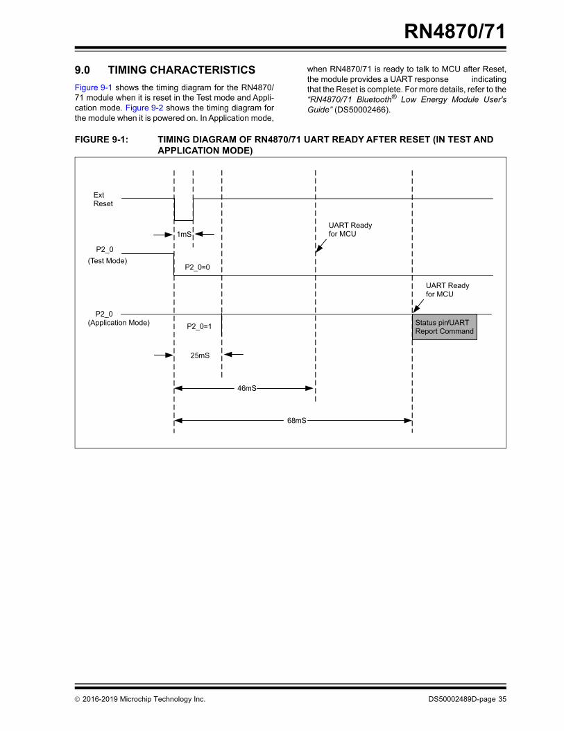
9.0 TIMING CHARACTERISTICSFigure 9-1 shows the timing diagram for the RN4870/71 module when it is reset in the Test mode and Appli-cation mode. Figure 9-2 shows the timing diagram for the module when it is powered on. In Application mode,when RN4870/71 is ready to talk to MCU after Reset, the module provides a UART response indicating that the Reset is complete. For more details, refer to the “RN4870/71 Bluetooth® Low Energy Module User's Guide” (DS50002466).
FIGURE 9-1: TIMING DIAGRAM OF RN4870/71 UART READY AFTER RESET (IN TEST AND APPLICATION MODE)
ExtReset
1mS
P2_0=0
P2_0=1
25mS
(Test Mode)P2_0
(Application Mode)P2_0
46mS
68mS
UART Readyfor MCU
UART Readyfor MCU
Status pin/UART Report Command
2016-2019 Microchip Technology Inc. DS50002489D-page 35
RN4870/71
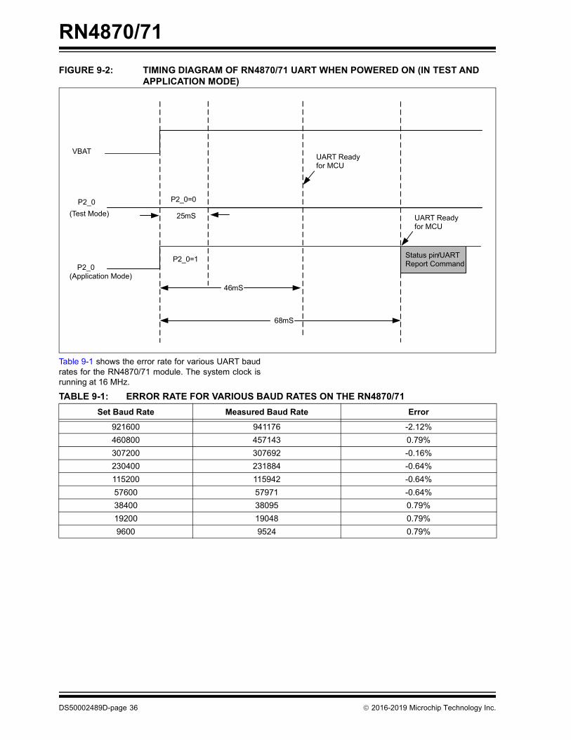
FIGURE 9-2: TIMING DIAGRAM OF RN4870/71 UART WHEN POWERED ON (IN TEST ANDAPPLICATION MODE)
Table 9-1 shows the error rate for various UART baud rates for the RN4870/71 module. The system clock is running at 16 MHz.
VBAT
P2_0=0
P2_0=1
25mS
46mS
68mS
UART Readyfor MCU
UART Readyfor MCU
Status pin/UART Report Command
(Test Mode)P2_0
(Application Mode)P2_0
TABLE 9-1: ERROR RATE FOR VARIOUS BAUD RATES ON THE RN4870/71 Set Baud Rate Measured Baud Rate Error
921600 941176 -2.12%460800 457143 0.79%307200 307692 -0.16%230400 231884 -0.64%115200 115942 -0.64%57600 57971 -0.64%38400 38095 0.79%19200 19048 0.79%9600 9524 0.79%
DS50002489D-page 36 2016-2019 Microchip Technology Inc.

RN4870/71
10.0 REGULATORY APPROVALThe RN4870 module has received the regulatory approval for the following countries:• United States/FCC ID: A8TBM70ABCDEFGH• Canada/ISED- IC: 12246A-BM70BLES1F2- HVIN: BM70BLES1F2
• Europe/CE• Japan/MIC: 202-SMD069• Korea/KCC: MSIP-CRM-mcp-BM70BLES1FC2 • Taiwan/NCC No: CCAN15LP0501T3• China/SRRC: CMIIT ID: 2016DJ5729The RN4871 module has received the regulatory approval for the following countries:• United States/FCC ID: A8TBM71S2• Canada/ISED
- IC: 12246A-BM71S2- HVIN: BM71BLES1FC2
• Europe/CE• Japan/MIC: 005-101150• Korea/KCC: MSIP-CRM-mcp-BM71BLES1FC2• Taiwan/NCC No: CCAN16LP0011T7• China/SRRC: CMIIT ID: 2016DJ5890
10.1 United StatesThe RN4870/71 module has received Federal Commu-nications Commission (FCC) CFR47 Telecommunica-tions, Part 15 Subpart C “Intentional Radiators” single-modular approval in accordance with Part 15.212 Mod-ular Transmitter approval. Single-modular transmitter approval is defined as a complete RF transmission sub-assembly, designed to be incorporated into another device, that must demonstrate compliance with FCC rules and policies independent of any host. A transmitter with a modular grant can be installed in dif-ferent end-use products (referred to as a host, host product, or host device) by the grantee or other equip-ment manufacturer, then the host product may not require additional testing or equipment authorization for the transmitter function provided by that specific module or limited module device.A host product itself is required to comply with all other applicable FCC equipment authorization regulations, requirements, and equipment functions that are not associated with the transmitter module portion. For example, compliance must be demonstrated: to regula-tions for other transmitter components within a host product; to requirements for unintentional radiators (Part 15 Subpart B), such as digital devices, computer peripherals, radio receivers, etc.; and to additional authorization requirements for the non-transmitter functions on the transmitter module (i.e., Verification or
Declaration of Conformity) as appropriate (e.g., Blue-tooth and Wi-Fi® transmitter modules may also contain digital logic functions).
10.1.1 LABELING AND USER INFORMATION REQUIREMENTS
The RN4870 module has been labeled with its own FCC ID number, and if the FCC ID is not visible when the module is installed inside another device, then the outside of the finished product into which the module is installed must also display a label referring to the enclosed module. This exterior label can use wording as follows:For the RN4870 module:
Due to the limited size of the RN4871, the FCC Identi-fier (FCC ID) is not displayed on the module. Therefore, the FCC ID must be placed on the outside of the fin-ished product into which the module is installed must also display a label referring to the enclosed module. This exterior label can use wording as follows:For the RN4871 module:
Contains Transmitter Module FCC ID: A8TBM70ABCDEFGHorContains FCC ID: A8TBM70ABCDEFGH
This device complies with Part 15 of the FCC Rules. Operation is subject to the following two conditions: (1) this device may not cause harmful interference, and (2) this device must accept any interference received, including interference that may cause undesired operation.
Contains Transmitter Module FCC ID: A8TBM71S2orContains FCC ID: A8TBM71S2
This device complies with Part 15 of the FCC Rules. Operation is subject to the following two conditions: (1) this device may not cause harmful interference, and (2) this device must accept any interference received, including interference that may cause undesired operation.
2016-2019 Microchip Technology Inc. DS50002489D-page 37

RN4870/71
A user’s manual for the product should include the fol-lowing statement:Additional information on labeling and user information requirements for Part 15 devices can be found in KDB Publication 784748 available at the FCC Office of Engi-neering and Technology (OET) Laboratory Division Knowledge Database (KDB) http://apps.fcc.gov/oetcf/kdb/index.cfm.
10.1.2 RF EXPOSUREAll transmitters regulated by FCC must comply with RF exposure requirements. KDB Publication 447498 Gen-eral RF Exposure Guidance provides guidance in determining whether proposed or existing transmitting facilities, operations or devices comply with limits for human exposure to Radio Frequency (RF) fields adopted by the Federal Communications Commission (FCC).Output power listed is conducted. This grant is valid only when the module is sold to OEM integrators and must be installed by the OEM or OEM integrators. This transmitter is restricted for use with the specific antenna(s) tested in this application for Certification and must not be co-located or operating in conjunction with any other antenna or transmitters within a host device, except in accordance with FCC multi-transmit-ter product procedures. This module is approved for installation into mobile or/and portable host platforms.
10.1.3 HELPFUL WEB SITESFederal Communications Commission (FCC): http://www.fcc.govFCC Office of Engineering and Technology (OET) Lab-oratory Division Knowledge Database (KDB): http://apps.fcc.gov/oetcf/kdb/index.cfm
10.2 CanadaThe RN4870/71 module has been certified for use in Canada under Innovation, Science and Economic Development Canada (ISED, formerly Industry Can-ada) Radio Standards Procedure (RSP) RSP-100, Radio Standards Specification (RSS) RSS-247 and RSS-Gen. Modular approval permits the installation of a module in a host device without the need to recertify the device.
10.2.1 LABELING AND USER INFORMATION REQUIREMENTS
Labeling Requirements for the Host product (from RSP-100-Issue 11, Section 3): The host product shall be properly labeled to identify the module within the host device.On the RN4871, due to the limited module size, the IC identifier is displayed in the data sheet only and it can-not be displayed on the module label.The Innovation, Science and Economic Development Canada certification label of a module shall be clearly visible at all times when installed in the host device; otherwise, the host device must be labeled to display the Innovation, Science and Economic Development Canada certification number of the module, preceded by the word “Contains”, or similar wording expressing the same meaning, as follows:For the RN4870 module:
For the RN4871 module:
This equipment has been tested and found to comply with the limits for a Class B digital device, pursuant to part 15 of the FCC Rules. These limits are designed to provide reasonable protection against harmful interference in a residential installation. This equip-ment generates, uses and can radiate radio fre-quency energy, and if not installed and used in accordance with the instructions, may cause harmful interference to radio communications. However, there is no guarantee that interference will not occur in a particular installation. If this equipment does cause harmful interference to radio or television reception, which can be determined by turning the equipment off and on, the user is encouraged to try to correct the interference by one or more of the follow-ing measures:• Reorient or relocate the receiving antenna.• Increase the separation between the equipment
and receiver.• Connect the equipment into an outlet on a circuit
different from that to which the receiver is con-nected.
• Consult the dealer or an experienced radio/TV technician for help.
Contains IC: 12246A-BM70BLES1F2
Contains IC: 12246A-BM71S2
DS50002489D-page 38 2016-2019 Microchip Technology Inc.

RN4870/71
User Manual Notice for License-Exempt Radio Appara-tus (from Section 8.4, RSS-Gen, Issue 4, November 2014): User manuals for license-exempt radio appara-tus shall contain the following or equivalent notice in a conspicuous location in the user manual or alterna-tively on the device or both:Guidelines on Transmitter Antenna for License Exempt Radio Apparatus:
10.2.2 RF EXPOSUREAll transmitters regulated by the Innovation, Science and Economic Development Canada (ISED) must comply with RF exposure requirements listed in RSS-102 - Radio Frequency (RF) Exposure Compliance of Radio communication Apparatus (All Frequency Bands).This transmitter is restricted for use with a specific antenna tested in this application for certification, and must not be co-located or operating in conjunction with
any other antenna or transmitters within a host device, except in accordance with Innovation, Science and Economic Development Canada multi-transmitter guidelines.The installation of the transmitter must ensure compli-ance is demonstrated according to the ISED SAR pro-cedures.
10.2.3 HELPFUL WEB SITESInnovation, Science and Economic Development Can-ada (ISED): http://www.ic.gc.ca/.
10.3 EuropeThe RN4870/71 module is an Radio Equipment Direc-tive (RED) assessed radio module that is CE marked and has been manufactured and tested with the inten-tion of being integrated into a final product. The RN4870/71 module has been tested to RED 2004/53/EC Essential Requirements for Health and Safety (Article (3.1(a)), Electromagnetic Compatibility (EMC) (Article 3.1(b)), and Radio (Article 3.2), which are summarized in the following European Compliance Testing tables. The ETSI provides guidance on modular devices in the “Guide to the application of harmonised standards cov-ering Article 3.1(b) and Article 3.2 of the Directive 2014/53/EU RED to multi-radio and combined radio and non-radio equipment” document available at http://www.etsi.org/deliver/etsi_eg/203300_203399/203367/01.01.01_60/eg_203367v010101p.pdf.
10.3.1 LABELING AND USER INFORMATION REQUIREMENTS
The label on the final product which contains the RN4870/71 module must follow CE marking require-ments.
This device complies with Industry Canada’s license-exempt RSS standard(s). Operation is subject to the following two conditions: (1) This device may not cause interference, and (2) This device must accept any interference, including interference that may cause undesired operation of the device.Le présent appareil est conforme aux CNR d'Industrie Canada applicables aux appareils radio exempts de licence. L'exploitation est autorisée aux deux conditions suivantes: (1) l'appareil ne doit pas produire de brouillage, et(2) l'utilisateur de l'appareil doit accepter tout brouillage radioélectrique subi, même si le brouil-lage est susceptible d'en compromettre le fonctionnement.
Under Industry Canada regulations, this radio transmitter may only operate using an antenna of a type and maximum (or lesser) gain approved for the transmitter by Industry Canada. To reduce potential radio interference to other users, the antenna type and its gain must be so chosen that the equivalent isotropically radiated power (e.i.r.p.) is not more than that necessary for suc-cessful communication.Conformément à la réglementation d'Industrie Canada, le présent émetteur radio peut fonction-ner avec une antenne d'un type et d'un gain max-imal (ou inférieur) approuvé pour l'émetteur par Industrie Canada. Dans le but de réduire les ris-ques de brouillage radioélectrique à l'intention des autres utilisateurs, il faut choisir le type d'antenne et son gain de sorte que la puissance isotrope rayonnée équivalente (p.i.r.e.) ne dépasse pas l'intensité nécessaire à l'établisse-ment d'une communication satisfaisante.
Note: To maintain conformance to the testing listed in Table 10-1/Table 10-2, the mod-ule shall be installed in accordance with the installation instructions in this data sheet and shall not be modified. When integrating a radio module into a completed product, the integrator becomes the manufacturer of the final product and is therefore responsible for demonstrating compliance of the final product with the essential requirements against the RED.
2016-2019 Microchip Technology Inc. DS50002489D-page 39

RN4870/71
Note 1: RF reports apply only to modules using the part IS1870SF-202.
Note 1: RF reports apply only to modules using the part IS1871SF-202.
10.3.2 CONFORMITY ASSESSMENTFrom ETSI Guidance Note EG 203367, section 6.1 Non-radio products are combined with a radio product:If the manufacturer of the combined equipment installs the radio product in a host non-radio product in equiva-lent assessment conditions (i.e. host equivalent to the one used for the assessment of the radio product) and according to the installation instructions for the radio product, then no additional assessment of the com-bined equipment against article 3.2 of the RED is required.The European Compliance Testing listed in Table 10-1 and Table 10-2 are performed using the integral ceramic chip antenna.
10.3.2.1 SIMPLIFIED EU DECLARATION OF CONFORMITY
Hereby, Microchip Technology Inc. declares that the radio equipment type RN4870/71 is in compliance with Directive 2014/53/EU.The full text of the EU declaration of conformity, for this product, is available at: http://www.microchip.com/design-centers/wireless-connectivity
TABLE 10-1: EUROPEAN COMPLIANCE TESTING (RN4870 MODULE)Certification Standards Article Laboratory Report Number DateSafety EN60950-1:2006/A11:2009/
A1:2010/A12:2011/A2:2013[3.1(a)]
TUV Rheinland
Taiwan
10051261 003 2016-01-05
Health EN300328 V1.9.1/ EN62479:2010
10053580 001 2015-12-10
EMC EN301489-1 V1.9.2 [3.1(b)]10051137 002 2016-01-08EN301489-17 V2.2.1
EN301489-1 V2.1.1EN301489-17 V2.2.0 10051137 003 2017-05-26EN301489-17 V3.1.1EN301489-17 V3.2.0
Radio EN300328 V1.9.1 (3.2) 10053580 001 2015-12-1050067510 001(1) 2016-01-04
EN300328 V2.1.1 50067510 002 2017-05-26
TABLE 10-2: EUROPEAN COMPLIANCE TESTING (RN4871 MODULE)Certification Standards Article Laboratory Report Number DateSafety EN60950-1:2006/A11:2009/
A1:2010/A12:2011/A2:2013[3.1(a)]
TUV Rheinland
Taiwan
10053210 001 2016-01-07
Health EN300328 V1.9.1/ EN62479:2010
10053433 001 2015-12-29
EMC EN301489-1 V1.9.2 [3.1(b)]10052964 001 2015-10-22EN301489-17 V2.2.1
EN301489-1 V2.1.1EN301489-1 V2.2.0 10052964 002 2017-05-26EN301489-17 V3.1.1EN301489-17 V3.2.0
Radio EN300328 V1.9.1 (3.2) 10053433 001 2015-12-2950067509 001(1) 2017-04-10
EN300328 V2.1.1 50067509 002 2017-05-26
DS50002489D-page 40 2016-2019 Microchip Technology Inc.

RN4870/71
10.3.3 HELPFUL WEB SITESA document that can be used as a starting point in understanding the use of Short Range Devices (SRD) in Europe is the European Radio Communications Committee (ERC) Recommendation 70-03 E, which can be downloaded from the European Radio Commu-nications Committee (ECC) at: http://www.ecodo-cdb.dk/.Additional helpful web sites are:• Radio Equipment Directive (2014/53/EU):https://ec.europa.eu/growth/single-market/euro-pean-standards/harmonised-standards/red_en
• European Conference of Postal and Telecommu-nications Administrations (CEPT): http://www.cept.org
• European Telecommunications Standards Insti-tute (ETSI): http://www.etsi.org
• The Radio Equipment Directive Compliance Association (REDCA): http://www.redca.eu/
10.4 JapanThe RN4870/71 module has received type certification and is labeled with its own technical conformity mark and certification number as required to conform to the technical standards regulated by the Ministry of Internal Affairs and Communications (MIC) of Japan pursuant to the Radio Act of Japan. Integration of this module into a final product does not require additional radio certification provided installa-tion instructions are followed and no modifications of the module are allowed. Additional testing may be required:• If the host product is subject to electrical appli-
ance safety (for example, powered from an AC mains), the host product may require Product Safety Electrical Appliance and Material (PSE) testing. The integrator should contact their confor-mance laboratory to determine if this testing is required.
• There is a voluntary Electromagnetic Compatibil-ity (EMC) test for the host product administered by VCCII: http://www.vcci.jp/vcci_e/index.html
10.4.1 LABELING AND USER INFORMATION REQUIREMENTS
The label on the final product which contains the RN4870/71 module must follow Japan marking requirements. The integrator of the module should refer to the labeling requirements for Japan available at the Ministry of Internal Affairs and Communications (MIC) website.
The RN4870 module is labeled with its own technical conformity mark and certification number. The final product in which this module is being used must have a label referring to the type certified module inside:
Due to the limited size of the RN4871, the technical conformity mark and certification number is not dis-played on the module. Therefore, the final product in which this module is being used must have a label referring to the type certified module inside:
10.4.2 HELPFUL WEB SITESMinistry of Internal Affairs and Communications (MIC): http://www.tele.soumu.go.jp/e/index.htm Association of Radio Industries and Businesses (ARIB): http://www.arib.or.jp/english/
10.5 KoreaThe RN4870/71 module has received certification of conformity in accordance with the Radio Waves Act. Integration of this module into a final product does not require additional radio certification provided installa-tion instructions are followed and no modifications of the module are allowed.
10.5.1 LABELING AND USER INFORMATION REQUIREMENTS
The label on the final product which contains the RN4870/71 module must follow KC marking require-ments. The integrator of the module should refer to the labeling requirements for Korea available on the Korea Communications Commission (KCC) website. The RN4870 module is labeled with its own KC mark. The final product requires the KC mark and certificate number of the module:
Contains transmitter module with certificate number:
Contains transmitter module with certificate number:
2016-2019 Microchip Technology Inc. DS50002489D-page 41

RN4870/71
Due to the limited size of the RN4871, the KC mark is not displayed on the module. Therefore, final product requires the KC mark and certificate number of the module:10.5.2 HELPFUL WEB SITESKorea Communications Commission (KCC): http://www.kcc.go.kr.National Radio Research Agency (RRA): http://rra.go.kr.
10.6 TaiwanThe RN4870/71 module has received compliance approval in accordance with the Telecommunications Act. Customers seeking to use the compliance approval in their product should contact Microchip Technology sales or distribution partners to obtain a Letter of Authority.Integration of this module into a final product does not require additional radio certification provided installa-tion instructions are followed and no modifications of the module are allowed.
10.6.1 LABELING AND USER INFORMATION REQUIREMENTS
The RN4870 module is labeled with its own NCC ID number, and if the NCC ID is not visible when the mod-ule is installed inside another device, then the outside of the device must also display a label referring to the enclosed module. This exterior label can use wording such as the following:
Due to the limited size of the RN4871, the NCC ID is not displayed on the module. Therefore, the outside of the device must also display a label referring to the enclosed module. This exterior label can use wording such as the following:
The user's manual should contain below warning (for RF device) in traditional Chinese:
注意 !依據 低功率電波輻射性電機管理辦法
第十二條 經型式認證合格之低功率射頻電機,
非經許可,
公司、商號或使用者均不得擅自變更頻率、加大
功率或變更原設計
之特性及功能。
第十四條 低功率射頻電機之使用不得影響飛航安
全及干擾合法通信;
經發現有干擾現象時,應立即停用,並改善至無
干擾時方得繼續使用。
前項合法通信,指依電信規定作業之無線電信。
低功率射頻電機須忍受合法通信或工業、科學及
醫療用電波輻射性
電機設備之干擾。
10.6.2 HELPFUL WEB SITESNational Communications Commission (NCC): http://www.ncc.gov.tw.
10.7 ChinaThe RN4870/71 module has received certification of conformity in accordance with the China MIIT Notice 2014-01 of State Radio Regulation Committee (SRRC) certification scheme. Integration of this module into a final product does not require additional radio certification, provided installation instructions are followed and no modifications of the module are allowed.
10.7.1 LABELING AND USER INFORMATION REQUIREMENTS
The RN4870 module is labeled with its own CMIT ID as follows:
The RN4871 module is labeled with its own CMIT ID as follows::
10.8 Other Regulatory JurisdictionsShould other regulatory jurisdiction certification be required by the customer, or the customer need to recertify the module for other reasons, a certification utility is available. For further regulatory Certification Utility and documentation, contact your local Microchip Technology sales office.
DS50002489D-page 42 2016-2019 Microchip Technology Inc.
RN4870/71
10.9 Other Regulatory Information• For information about other countries jurisdictionsnot covered here, refer to the http://www.micro-chip.com/design-centers/wireless-connectivity.
• Should other regulatory jurisdiction certification be required by the customer, or the customer needs to recertify the module for other reasons, contact Microchip for the required utilities and documentation.
2016-2019 Microchip Technology Inc. DS50002489D-page 43

RN4870/71
NOTES:DS50002489D-page 44 2016-2019 Microchip Technology Inc.

2016-2019 Microchip Technology Inc. DS50002489D-page 45
RN4870/7111.0 ORDERING INFORMATIONTable 11-1 provides ordering information for the RN4870/71 module.
Go to http://www.microchip.com for current pricing and a list of distributors carrying Microchip products.
TABLE 11-1: ORDERING INFORMATION
Part Number(1) Antenna Shielding Number of Pins Operating Temperature Range
RN4870-V/RMXXX On-Board Yes 33 -20°C to +70°CRN4870U-V/RMXXX External No 30 -20°C to +70°CRN4871-V/RMXXX On-Board Yes 16 -20°C to +70°CRN4871U-V/RMXXX External No 17 -20°C to +70°CRN4870-I/RMXXX On-Board Yes 33 -40°C to +85°CRN4871-I/RMXXX On-Board Yes 16 -40°C to +85°CNote 1: The last three digits in P/N indicate firmware version. At the time of publication, the latest firmware version
is 1.30. Ensure to check product webpage for latest part number and firmware version.

RN4870/71
DS50002489D-page 46 2016-2019 Microchip Technology Inc.
APPENDIX A: REVISION HISTORY
Revision A (April 2016)This is the initial release of this document.
Revision B (October 2017)• Added the new parts, RN4870-I/RMXXX and
RN4871-I/RMXXX, released with increased operating temperature range.
• Updated Features section and removed Description section on page 1.
• Updated Table 1-1, Table 1-2, Table 1-4 and Table 11-1.
• Revised Table 2-1 through Table 2-4.• Updated Figure 1-4, Figure 3-1, Figure 3-2, and
Figure 4-7.• Added Section 10.7 “China” to Section 10.0
“Regulatory Approval”;• Updated Table 11-1 and Section “Product
Identification System”.
Revision C (December 2017)• Updated Table 2-1 to correct information for the
operating temperature range.
Revision D (April 2019) • Updated Bluetooth version from 4.2 to 5.0.• Updated Features and Antenna Options. • Updated Figure 5-2, Figure 5-3, Figure 5-4, and
Figure 5-5. • Updated Figure 9-1 and Figure 9-2 (P2_0 = 1)• Updated Section 7.0 “Supported Services”• Updated Section 10.2 “Canada” and
Section 10.3 “Europe”

RN4870/71
THE MICROCHIP WEBSITEMicrochip provides online support via our WWW site atwww.microchip.com. This website is used as a meansto make files and information easily available tocustomers. Accessible by using your favorite Internetbrowser, the website contains the following information:• Product Support – Data sheets and errata,
application notes and sample programs, design resources, user’s guides and hardware support documents, latest software releases and archived software
• General Technical Support – Frequently Asked Questions (FAQ), technical support requests, online discussion groups, Microchip consultant program member listing
• Business of Microchip – Product selector and ordering guides, latest Microchip press releases, listing of seminars and events, listings of Microchip sales offices, distributors and factory representatives
CUSTOMER CHANGE NOTIFICATION SERVICEMicrochip’s customer notification service helps keepcustomers current on Microchip products. Subscriberswill receive e-mail notification whenever there arechanges, updates, revisions or errata related to aspecified product family or development tool of interest.To register, access the Microchip website atwww.microchip.com. Under “Support”, click on“Customer Change Notification” and follow theregistration instructions.
CUSTOMER SUPPORTUsers of Microchip products can receive assistancethrough several channels:• Distributor or Representative• Local Sales Office• Field Application Engineer (FAE)• Technical SupportCustomers should contact their distributor,representative or Field Application Engineer (FAE) forsupport. Local sales offices are also available to helpcustomers. A listing of sales offices and locations isincluded in the back of this document.Technical support is available through the websiteat: http://microchip.com/support
2015-2019 Microchip Technology Inc. DS50002489D-page 47

RN4870/71
NOTES:
2015-2019 Microchip Technology Inc. DS50002489D-page 48

RN4870/71
DS50002489D-page 49 2016-2019 Microchip Technology Inc.
PRODUCT IDENTIFICATION SYSTEMTo order or obtain information, for example, on pricing or delivery, refer to the factory or the listed sales office.
Device: RN4870: Ceramic Chip Antenna
RN4870U: External AntennaRN4871: Ceramic Chip AntennaRN4871U: External Antenna
Temperature Range:
V = -20C to +70C (Various)I = -40C to +85C (Industrial)
Package: RM = Radio Module
Example:RN4870-V/RM118: Various temperature
RN4870-I/RM128: Industrial temperature
Note 1: Tape and Reel identifier only appears in the catalog part number description. This identifier is used for ordering purposes and is not printed on the device package. Check with your Microchip Sales Office for package availability with the Tape and Reel option.
PART NO.
Device
V
TemperatureRange
RM
Package
XXX
Firmware Revision Number
Note the following details of the code protection feature on Microchip devices:• Microchip products meet the specification contained in their particular Microchip Data Sheet.
• Microchip believes that its family of products is one of the most secure families of its kind on the market today, when used in the intended manner and under normal conditions.
• There are dishonest and possibly illegal methods used to breach the code protection feature. All of these methods, to our knowledge, require using the Microchip products in a manner outside the operating specifications contained in Microchip’s Data Sheets. Most likely, the person doing so is engaged in theft of intellectual property.
• Microchip is willing to work with the customer who is concerned about the integrity of their code.
• Neither Microchip nor any other semiconductor manufacturer can guarantee the security of their code. Code protection does not mean that we are guaranteeing the product as “unbreakable.”
Code protection is constantly evolving. We at Microchip are committed to continuously improving the code protection features of ourproducts. Attempts to break Microchip’s code protection feature may be a violation of the Digital Millennium Copyright Act. If such actsallow unauthorized access to your software or other copyrighted work, you may have a right to sue for relief under that Act.
Information contained in this publication regarding deviceapplications and the like is provided only for your convenienceand may be superseded by updates. It is your responsibility toensure that your application meets with your specifications.MICROCHIP MAKES NO REPRESENTATIONS ORWARRANTIES OF ANY KIND WHETHER EXPRESS ORIMPLIED, WRITTEN OR ORAL, STATUTORY OROTHERWISE, RELATED TO THE INFORMATION,INCLUDING BUT NOT LIMITED TO ITS CONDITION,QUALITY, PERFORMANCE, MERCHANTABILITY ORFITNESS FOR PURPOSE. Microchip disclaims all liabilityarising from this information and its use. Use of Microchipdevices in life support and/or safety applications is entirely atthe buyer’s risk, and the buyer agrees to defend, indemnify andhold harmless Microchip from any and all damages, claims,suits, or expenses resulting from such use. No licenses areconveyed, implicitly or otherwise, under any Microchipintellectual property rights unless otherwise stated.
2019 Microchip Technology Inc.
Microchip received ISO/TS-16949:2009 certification for its worldwide headquarters, design and wafer fabrication facilities in Chandler and Tempe, Arizona; Gresham, Oregon and design centers in California and India. The Company’s quality system processes and procedures are for its PIC® MCUs and dsPIC® DSCs, KEELOQ® code hopping devices, Serial EEPROMs, microperipherals, nonvolatile memory and analog products. In addition, Microchip’s quality system for the design and manufacture of development systems is ISO 9001:2000 certified.
QUALITY MANAGEMENT SYSTEM CERTIFIED BY DNV
== ISO/TS 16949 ==
TrademarksThe Microchip name and logo, the Microchip logo, AnyRate, AVR, AVR logo, AVR Freaks, BitCloud, chipKIT, chipKIT logo, CryptoMemory, CryptoRF, dsPIC, FlashFlex, flexPWR, Heldo, JukeBlox, KeeLoq, Kleer, LANCheck, LINK MD, maXStylus, maXTouch, MediaLB, megaAVR, MOST, MOST logo, MPLAB, OptoLyzer, PIC, picoPower, PICSTART, PIC32 logo, Prochip Designer, QTouch, SAM-BA, SpyNIC, SST, SST Logo, SuperFlash, tinyAVR, UNI/O, and XMEGA are registered trademarks of Microchip Technology Incorporated in the U.S.A. and other countries.ClockWorks, The Embedded Control Solutions Company, EtherSynch, Hyper Speed Control, HyperLight Load, IntelliMOS, mTouch, Precision Edge, and Quiet-Wire are registered trademarks of Microchip Technology Incorporated in the U.S.A.Adjacent Key Suppression, AKS, Analog-for-the-Digital Age, Any Capacitor, AnyIn, AnyOut, BodyCom, CodeGuard, CryptoAuthentication, CryptoAutomotive, CryptoCompanion, CryptoController, dsPICDEM, dsPICDEM.net, Dynamic Average Matching, DAM, ECAN, EtherGREEN, In-Circuit Serial Programming, ICSP, INICnet, Inter-Chip Connectivity, JitterBlocker, KleerNet, KleerNet logo, memBrain, Mindi, MiWi, motorBench, MPASM, MPF, MPLAB Certified logo, MPLIB, MPLINK, MultiTRAK, NetDetach, Omniscient Code Generation, PICDEM, PICDEM.net, PICkit, PICtail, PowerSmart, PureSilicon, QMatrix, REAL ICE, Ripple Blocker, SAM-ICE, Serial Quad I/O, SMART-I.S., SQI, SuperSwitcher, SuperSwitcher II, Total Endurance, TSHARC, USBCheck, VariSense, ViewSpan, WiperLock, Wireless DNA, and ZENA are trademarks of Microchip Technology Incorporated in the U.S.A. and other countries.SQTP is a service mark of Microchip Technology Incorporated in the U.S.A.Silicon Storage Technology is a registered trademark of Microchip Technology Inc. in other countries.GestIC is a registered trademark of Microchip Technology Germany II GmbH & Co. KG, a subsidiary of Microchip Technology Inc., in other countries. All other trademarks mentioned herein are property of their respective companies.© 2018, Microchip Technology Incorporated, All Rights Reserved.ISBN: 978-1-5224-4453-4
DS50002489D-page 50

DS50002489D-page 51 2019 Microchip Technology Inc.
AMERICASCorporate Office2355 West Chandler Blvd.Chandler, AZ 85224-6199Tel: 480-792-7200 Fax: 480-792-7277Technical Support: http://www.microchip.com/supportWeb Address: www.microchip.comAtlantaDuluth, GA Tel: 678-957-9614 Fax: 678-957-1455Austin, TXTel: 512-257-3370 BostonWestborough, MA Tel: 774-760-0087 Fax: 774-760-0088ChicagoItasca, IL Tel: 630-285-0071 Fax: 630-285-0075DallasAddison, TX Tel: 972-818-7423 Fax: 972-818-2924DetroitNovi, MI Tel: 248-848-4000Houston, TX Tel: 281-894-5983IndianapolisNoblesville, IN Tel: 317-773-8323Fax: 317-773-5453Tel: 317-536-2380Los AngelesMission Viejo, CA Tel: 949-462-9523Fax: 949-462-9608Tel: 951-273-7800 Raleigh, NC Tel: 919-844-7510New York, NY Tel: 631-435-6000San Jose, CA Tel: 408-735-9110Tel: 408-436-4270Canada - TorontoTel: 905-695-1980 Fax: 905-695-2078
ASIA/PACIFICAustralia - SydneyTel: 61-2-9868-6733China - BeijingTel: 86-10-8569-7000 China - ChengduTel: 86-28-8665-5511China - ChongqingTel: 86-23-8980-9588China - DongguanTel: 86-769-8702-9880 China - GuangzhouTel: 86-20-8755-8029 China - HangzhouTel: 86-571-8792-8115 China - Hong Kong SARTel: 852-2943-5100 China - NanjingTel: 86-25-8473-2460China - QingdaoTel: 86-532-8502-7355China - ShanghaiTel: 86-21-3326-8000 China - ShenyangTel: 86-24-2334-2829China - ShenzhenTel: 86-755-8864-2200 China - SuzhouTel: 86-186-6233-1526 China - WuhanTel: 86-27-5980-5300China - XianTel: 86-29-8833-7252China - XiamenTel: 86-592-2388138 China - ZhuhaiTel: 86-756-3210040
ASIA/PACIFICIndia - BangaloreTel: 91-80-3090-4444 India - New DelhiTel: 91-11-4160-8631India - PuneTel: 91-20-4121-0141Japan - OsakaTel: 81-6-6152-7160 Japan - TokyoTel: 81-3-6880- 3770 Korea - DaeguTel: 82-53-744-4301Korea - SeoulTel: 82-2-554-7200Malaysia - Kuala LumpurTel: 60-3-7651-7906Malaysia - PenangTel: 60-4-227-8870Philippines - ManilaTel: 63-2-634-9065SingaporeTel: 65-6334-8870Taiwan - Hsin ChuTel: 886-3-577-8366Taiwan - KaohsiungTel: 886-7-213-7830Taiwan - TaipeiTel: 886-2-2508-8600 Thailand - BangkokTel: 66-2-694-1351Vietnam - Ho Chi MinhTel: 84-28-5448-2100
EUROPEAustria - WelsTel: 43-7242-2244-39Fax: 43-7242-2244-393Denmark - CopenhagenTel: 45-4450-2828 Fax: 45-4485-2829Finland - EspooTel: 358-9-4520-820France - ParisTel: 33-1-69-53-63-20 Fax: 33-1-69-30-90-79 Germany - GarchingTel: 49-8931-9700Germany - HaanTel: 49-2129-3766400Germany - HeilbronnTel: 49-7131-67-3636Germany - KarlsruheTel: 49-721-625370Germany - MunichTel: 49-89-627-144-0 Fax: 49-89-627-144-44Germany - RosenheimTel: 49-8031-354-560Israel - Ra’anana Tel: 972-9-744-7705Italy - Milan Tel: 39-0331-742611 Fax: 39-0331-466781Italy - PadovaTel: 39-049-7625286 Netherlands - DrunenTel: 31-416-690399 Fax: 31-416-690340Norway - TrondheimTel: 47-7288-4388Poland - WarsawTel: 48-22-3325737 Romania - BucharestTel: 40-21-407-87-50Spain - MadridTel: 34-91-708-08-90Fax: 34-91-708-08-91Sweden - GothenbergTel: 46-31-704-60-40Sweden - StockholmTel: 46-8-5090-4654UK - WokinghamTel: 44-118-921-5800Fax: 44-118-921-5820
Worldwide Sales and Service
08/15/18