robust to pvt high dc gain amplifier for ct … · en este trabajo son propuestos dos otas. como...
TRANSCRIPT
Robust to PVT, High DCGain Amplifier for CT Σ∆Modulators on SOI CMOS
Technology
by
Hector Ivan Gomez Ortiz
Dissertation submitted as partial fulfillment of therequirements for the degree of
MASTER ON SCIENCE WITH MAJOR ONELECTRONICS
fromNational Institute for Astrophysics, Optics and
ElectronicsOctober 2011
Tonantzintla, Puebla
Supervised by:
Ph.D. Guillermo Espinosa Flores-Verdad,INAOE
c©INAOE 2011The author hereby grants to INAOE permission toreproduce and to distribute copies of this Thesis in
whole or in part.

.
“ To my parents Arleth and Luis Hector
To my sister Mabel and my brother Diego
To Jennifer ”
Hector.

Acknowledgment
First of all to God for all his blessings.
I want to thank my parents Arleth and Luis Hector and my sister Mabel and my brother Diego for all
their understanding and support. Without them, nothing that so far I’ve managed, it had been
possible.
I would like to thank my girlfriend Jennifer because despite the distance always she knew giving me
her love and support.
I would like to thank my advisor Ph.D. Guillermo Espinosa Flores-Verdad for his useful advices and
support.
I would like to thank Juan Carlos, Ricardo, Luz Karine, Jhoan and Fabian for their friendship and
their collaboration in some way with development of this project.
I want to thank CONACyT for my scholarship.
In general, I want to thank INAOE.

ABSTRACT
TITLE: Robust to PVT High DC gain Amplifier for CT Σ∆ Modulators on SOI CMOS Technology 1.
AUTHORS: HECTOR IVAN GOMEZ ORTIZ
KEY WORDS: SOI, PVT, OTA, buffer, Σ∆ modulator, continuous time.
DESCRIPTION: SOI technology is particularly good for low voltage, low power and high speed
digital systems because it has reduced drain to substrate capacitance due to the inclusion of an insu-
lator layer between substrate and active region. Nonetheless, SOI is a pure digital technology making
the analog design a challenging task. This work present the design of a relatively high DC gain ampli-
fier on SOI technology, which must be robust to PVT variations. In order to evaluate the performance
of amplifier, it is used in a continuous time sigma delta modulator.
Two OTAs was proposed in this work. As a first consideration, self-cascode transistor was used to
improve the output impedance and reduce the influence of voltage supply in the amplifier gain. Also,
a current shunt technique was applied to first proposed amplifier to enhance DC gain. However, the
PVT variations considerably affects the performance of amplifier, so a second proposal was accom-
plished. Sums of transconductance was used together self-cascode transistor to reduce sensitivity to
PVT variations. The last proposed amplifier achieves a DC gain of 53 dB with GBW=575 MHz and a
power consumption of 1.25 mW. Simulation results shows that the amplifier has a DC gain over 50 dB
despite PVT variations.
To drive resistive load of the first integrator of the modulator, different buffer was proposed in
order to have wide input and output voltage excursion and low output impedance. Final Buffer im-
plementation is a feedback amplifier which has complementary input differential pairs and a class AB
output stage. Open loop gain of the amplifier is 57 dB while has close loop output impedance of
55 Ω. Buffer’s harmonic distortion is around 0.1 % for all PVT variations with a voltage excursion of
600 mV.
A comparison between two-stage Miller amplifier and proposed amplifier was done to see how
PVT variations affect the performance of a commonly used amplifier. Finally, both amplifiers are in-
cluded in the modulator to validate the robustness of the proposed amplifier. Simulations of the whole
modulator show that the SNDR of modulator is improved over 9 dB using the proposed amplifier.
The design was done on SOI 45 nm IBM technology and simulations were carried out in Hspice.
1Master thesis.

RESUMEN
TITULO: Amplificador robusto a PVT con alta ganancia en DC para moduladores Σ∆ en tiempo
continuo en tecnologıa SOI 2
AUTOR: HECTOR IVAN GOMEZ ORTIZ
PALABRAS CLAVES:SOI, PVT, OTA, Buffer, modulador Σ∆, tiempo continuo.
DESCRIPCION: La tecnologıa SOI es particularmente buena para bajo voltaje, baja potencia y sis-
temas digitales de alta velocidad, por que tiene una capacitancia de drenaje a substrato reducida debido
a la inclusion de una capa de aislante entre el substrato y la region activa. Sin embargo, SOI es una
tecnologıa puramente digital lo que hace de el diseno analogico un tarea desafiante. En este trabajo se
presenta el diseno de un amplificador con relativa alta ganancia en DC en tecnologıa SOI, el cual debe
ser robusto a variaciones de PVT. Con el fin de evaluar el desempeno del amplificador, este se usa en
un modulador sigma delta en tiempo continuo.
En este trabajo son propuestos dos OTAs. Como primera consideracion, se usan transistores com-
puestos para aumentar la impedancia de salida del amplificador y reducir la influencia del voltaje de
alimentacion en la ganancia del amplificador. Ademas, se usa una tecnica de derivacion de corriente en
el el primer amplificador propuesto para aumentar la ganancia de DC. Sin embargo, las variaciones de
PVT afectan considerablemente el desempeno del amplificador por lo cual se propone un segundo am-
plificador. Se usa una suma de transconductancias junto con transistores compuestos para reducir las
efectos de las variaciones PVT. El ultimo amplificador propuesto logra una ganancia en DC de 53 dB
con GBW=575 MHz y un consumo de potencia de 1.25mW. Los resultados de simulacion muestran
que el amplificador mantiene una ganancia en DC de mas de 50 dB a pesar de las variaciones de PVT.
Para manejar la carga resistiva del primer integrador del modulador, se propusieron diferentes
buffers con el fin de obtener amplios rangos de excursion de voltaje a la entrada y a la salida y una
baja impedancia de salida. La implementacion final del buffer es una amplificador realimentado el cual
tiene pares diferenciales complementarios a la entrada y una etapa de salida clase AB. La ganancia
en lazo abierto del amplificador es 57 dB mientras tiene una impedancia de salida en lazo cerrado de
55 Ω. La distorsion harmonica del buffer es alrededor de 0.1 % para todas las variaciones de PVT con
una excursion de voltaje de 600 mV.
Se hace una comparacion entre un amplificador Miller de dos etapas y el amplificador propuesto
para ver como las variaciones de PVT afectan el desempeno de un amplificador comunmente usado.
Finalmente, ambos amplificadores se utilizan en un modulador para validar la robustez del amplifi-
2Tesis de maestrıa.

v
cador propuesto. Las simulaciones del modulador muestran que si mejora la SNDR del modulador en
mas de 9 dB usando el amplificador propuesto.
El diseno fue hecho en una tecnologıa SOI de 45 nm de IBM y las simulaciones se realizaron en
Hspice.

vi

Contents
1 Introduction 1
1.1 Basic theory of Σ∆ modulation . . . . . . . . . . . . . . . . . . . . . . . . . . . . 2
1.1.1 Performance metrics . . . . . . . . . . . . . . . . . . . . . . . . . . . . . . 4
1.2 Silicon-On-Insulator technology . . . . . . . . . . . . . . . . . . . . . . . . . . . . 5
1.2.1 SOI MOSFET’s junction diode . . . . . . . . . . . . . . . . . . . . . . . . . 6
1.2.2 Impact Ionization . . . . . . . . . . . . . . . . . . . . . . . . . . . . . . . . 6
1.2.3 Floating body effects . . . . . . . . . . . . . . . . . . . . . . . . . . . . . . 7
1.3 State of the art for CT Σ∆ Modulators. . . . . . . . . . . . . . . . . . . . . . . . . 9
1.4 Dissertation Organization . . . . . . . . . . . . . . . . . . . . . . . . . . . . . . . . 10
2 Theory and modeling of CT Σ∆ modulators 11
2.1 Issues and Operation of the Modulator . . . . . . . . . . . . . . . . . . . . . . . . . 11
2.1.1 Sampling Operation . . . . . . . . . . . . . . . . . . . . . . . . . . . . . . 12
2.1.2 Filter Realization . . . . . . . . . . . . . . . . . . . . . . . . . . . . . . . . 13
2.1.3 Quantizer Implementation . . . . . . . . . . . . . . . . . . . . . . . . . . . 14
2.1.4 Feedback Realization . . . . . . . . . . . . . . . . . . . . . . . . . . . . . . 14
2.2 Modeling and Simulation at System Level . . . . . . . . . . . . . . . . . . . . . . . 16
2.2.1 Considering the Effects of Gain and Finite Bandwidth . . . . . . . . . . . . 16
2.2.2 Clock Jitter . . . . . . . . . . . . . . . . . . . . . . . . . . . . . . . . . . . 18
2.2.3 Other Non-Indealities . . . . . . . . . . . . . . . . . . . . . . . . . . . . . . 19
2.2.4 Example of Modeling a Modulator . . . . . . . . . . . . . . . . . . . . . . . 19
2.3 Simulations at system level of the proposed modulator . . . . . . . . . . . . . . . . 24
3 Design and Simulations of the Proposed Circuits 27
3.1 Gain-Enhancement . . . . . . . . . . . . . . . . . . . . . . . . . . . . . . . . . . . 27
3.2 Final implementation of the amplifier . . . . . . . . . . . . . . . . . . . . . . . . . 31
3.2.1 Circuit implementation of proposed topology . . . . . . . . . . . . . . . . . 32
3.2.2 Design and simulations . . . . . . . . . . . . . . . . . . . . . . . . . . . . . 33
viii CONTENTS
3.3 Comparison of topologies . . . . . . . . . . . . . . . . . . . . . . . . . . . . . . . . 36
3.3.1 Process variations . . . . . . . . . . . . . . . . . . . . . . . . . . . . . . . . 36
3.3.2 Process, Voltage and Temperature Variations . . . . . . . . . . . . . . . . . 36
3.4 Loop Filter . . . . . . . . . . . . . . . . . . . . . . . . . . . . . . . . . . . . . . . 37
3.4.1 Proposing a Buffer . . . . . . . . . . . . . . . . . . . . . . . . . . . . . . . 38
4 Results 414.1 Whole System Implementation . . . . . . . . . . . . . . . . . . . . . . . . . . . . . 41
4.1.1 VerilogA Implementation . . . . . . . . . . . . . . . . . . . . . . . . . . . . 41
4.1.2 Simulations Results Using the Proposed Circuits . . . . . . . . . . . . . . . 42
4.1.3 PVT analysis . . . . . . . . . . . . . . . . . . . . . . . . . . . . . . . . . . 44
4.2 Comparison of Topologies Used . . . . . . . . . . . . . . . . . . . . . . . . . . . . 45
5 Conclusions 475.1 Future works . . . . . . . . . . . . . . . . . . . . . . . . . . . . . . . . . . . . . . 48
Bibliography 49
List of Figures
1.1 Σ∆ DT model. . . . . . . . . . . . . . . . . . . . . . . . . . . . . . . . . . . . . . 3
1.2 Critical performance of an ADC (a) output frequency spectrum (b) output power com-
ponent v.s. input signal power. [6]. . . . . . . . . . . . . . . . . . . . . . . . . . . . 4
1.3 Cross-section of bulk and SOI MOS devices. . . . . . . . . . . . . . . . . . . . . . 5
1.4 Roll-off of threshold voltage with Leff for bulk and SOI devices [9]. . . . . . . . . . 8
2.1 Block diagram of a CT Σ∆ A/D converter [3]. . . . . . . . . . . . . . . . . . . . . . 11
2.2 Equivalent representation of a CT Σ∆ modulator considering its implicit AAF [3]. . 13
2.3 Feedback DAC waveforms. . . . . . . . . . . . . . . . . . . . . . . . . . . . . . . . 15
2.4 OpAmp RC integrator with multiple inputs. . . . . . . . . . . . . . . . . . . . . . . 17
2.5 Real integrator model [23]. . . . . . . . . . . . . . . . . . . . . . . . . . . . . . . . 18
2.6 Modeling a random sampling jitter [24]. . . . . . . . . . . . . . . . . . . . . . . . . 18
2.7 Input-referred noise and distortion model [6]. . . . . . . . . . . . . . . . . . . . . . 19
2.8 Third order modulator including ELD compensation [13]. . . . . . . . . . . . . . . . 19
2.9 Simulink model of the third order modulator. . . . . . . . . . . . . . . . . . . . . . 21
2.10 Ideal dynamic range and peak SNR for third order modulator. . . . . . . . . . . . . . 21
2.11 Effect of white noise added to integrators for third order modulator. . . . . . . . . . 22
2.12 Influence of harmonic distortion of amplifiers for third order modulator. . . . . . . . 22
2.13 Considering the effect of GBW and finite gain for third order modulator. . . . . . . . 22
2.14 Effect of jitter noise for third order modulator. . . . . . . . . . . . . . . . . . . . . . 23
2.15 CT Σ∆ modulator at system level. . . . . . . . . . . . . . . . . . . . . . . . . . . . 24
2.16 Ideal dynamic range and peak SNDR of proposed modulator. . . . . . . . . . . . . . 25
2.17 Amplifier gain effect in the performance of the proposed modulator. . . . . . . . . . 26
2.18 Dynamic range and peak SNDR including amplifier’s non-idealities in the proposed
modulator. . . . . . . . . . . . . . . . . . . . . . . . . . . . . . . . . . . . . . . . . 26
3.1 Self-cascode transistor. . . . . . . . . . . . . . . . . . . . . . . . . . . . . . . . . . 28
3.2 Two stage Miller amplifier. . . . . . . . . . . . . . . . . . . . . . . . . . . . . . . . 28
x LIST OF FIGURES
3.3 Amplifier with bidirectional output drive. . . . . . . . . . . . . . . . . . . . . . . . 29
3.4 Current shunt. . . . . . . . . . . . . . . . . . . . . . . . . . . . . . . . . . . . . . . 29
3.5 Amplifier with gain improvement. . . . . . . . . . . . . . . . . . . . . . . . . . . . 30
3.6 Frequency response of the Amplifier with gain improvement. . . . . . . . . . . . . . 30
3.7 Block diagram of OTA. . . . . . . . . . . . . . . . . . . . . . . . . . . . . . . . . . 31
3.8 Enhanced amplifier with gain improvement. . . . . . . . . . . . . . . . . . . . . . . 32
3.9 CMFB circuit. . . . . . . . . . . . . . . . . . . . . . . . . . . . . . . . . . . . . . . 33
3.10 Performance of the enhanced amplifier : (a) and (b) show frequency response; (c)
output voltage excursion; (d) transient response with output excursion of 500 mV. . . 34
3.11 Process variations with temperature and nominal voltage:(a) and (c) frequency re-
sponse of Miller amplfier, (b) and (d) frequency response of enhanced amplifier. . . . 35
3.12 PVT variations of studied topologies. . . . . . . . . . . . . . . . . . . . . . . . . . . 35
3.13 Loop filter. . . . . . . . . . . . . . . . . . . . . . . . . . . . . . . . . . . . . . . . . 37
3.14 Effect of OTA output impedance in filter frequency response. . . . . . . . . . . . . . 38
3.15 Block diagram of the fully differential buffer. . . . . . . . . . . . . . . . . . . . . . 38
3.16 Fully differential buffer. . . . . . . . . . . . . . . . . . . . . . . . . . . . . . . . . . 39
3.17 Block diagram of a single ended buffer. . . . . . . . . . . . . . . . . . . . . . . . . 39
3.18 Single ended buffers. . . . . . . . . . . . . . . . . . . . . . . . . . . . . . . . . . . 40
3.19 Process variations for proposed the buffer. . . . . . . . . . . . . . . . . . . . . . . . 40
4.1 Whole system implementation. . . . . . . . . . . . . . . . . . . . . . . . . . . . . . 42
4.2 Power spectrum of system described in VerilogA. . . . . . . . . . . . . . . . . . . . 42
4.3 Dynamic range and peak SNDR of proposed modulator. . . . . . . . . . . . . . . . . 43
4.4 Power spectrum with increment of IBN at low frequency. . . . . . . . . . . . . . . . 43
4.5 Effect of variations on voltage supply. . . . . . . . . . . . . . . . . . . . . . . . . . 45
4.6 Output Power spectrum of the modulator: with miller amplifier (a) and with enhanced
OTA (b). . . . . . . . . . . . . . . . . . . . . . . . . . . . . . . . . . . . . . . . . . 45

List of Tables
1.1 Literature survey of the reported Σ∆ ADCs. . . . . . . . . . . . . . . . . . . . . . . 9
2.1 Coefficients of modulator. . . . . . . . . . . . . . . . . . . . . . . . . . . . . . . . . 20
3.1 Dimensions of enhanced amplifier. . . . . . . . . . . . . . . . . . . . . . . . . . . . 33
3.2 Dimensions of Miller amplifier. . . . . . . . . . . . . . . . . . . . . . . . . . . . . . 33
3.3 Circuit specification of the Miller amplifier . . . . . . . . . . . . . . . . . . . . . . 36
3.4 Circuit specification of the enhanced amplifier. . . . . . . . . . . . . . . . . . . . . 36
3.5 Resistor and capacitor values. . . . . . . . . . . . . . . . . . . . . . . . . . . . . . . 37
4.1 Performance summary. SNR and SNDR are expressed in dB. . . . . . . . . . . . . 44

xii LIST OF TABLES
List of Abbreviations
Σ∆ Sigma Delta
ADC Analog to Digital Converter
CMFB Common Mode Feedback
CT Continuous Time
DAC Digital to Analog Converter
DR Dynamic Range
DT Discrete Time
ELD Excess Loop Delay
ENOB Effective Number of Bits
GBW Gain Bandwidth
IBN In Band Noise
IM3 Third Order Intermodulation Distortion
OTA Operational Transconductance Amplifier
PVT Process Temperature and Voltage
SCE Short Channel Effect
SFDR Spurious Free Dynamic Range
SNDR Signal to Noise and Distortion Ratio
SNR Signal to Noise Ratio
SOI Silicon On Insulator

xiv LIST OF TABLES
SQNR Signal to Quantization Noise Ratio
THD Total Harmonic Distortion
Chapter 1
Introduction
The technology scaling has originated a contrast on integrated circuit design. While the digital cir-
cuits have a performance improvement related to their higher speed operation and power consumption
saving, the analog circuits show some negative effects such as reduced dynamic range, higher noise
and loss in the intrinsic gain of transistors. As a consequence, there has been a trend of moving more
functionality into the digital domain.
Although much of the processing is done in the digital domain, there is still the need of an element
that provides a link between digital and analog domain: the analog-to-digital converter (ADC). Its
design has been investigated in the last years motivated by the rapid growth of the market for portable
systems and the integration on-chip of the analog-to-digital interface. However, the required specifi-
cations in different applications make the ADC design a challenging task because it is necessary to
achieve high linearity, dynamic range and bandwidth capabilities, which conflicts with the low-power
requirements for long stand-by time [1].
There exist a lot of possibilities to implement analog to digital (A/D) conversion depending on
the resolution or the speed of data conversion. One favorable option, especially in very large scale
integration (VLSI) systems, is the sigma–delta (Σ∆) ADC which shows a very low sensitivity to the
non-idealities of its building blocks, besides simplifying analog functions like pre-filtering [2]. It
is common to find two kind of implementations of a Σ∆ (modulator) ADC: discrete-time (DT) and
continuous-time (CT). The switched capacitor (SC) technique made very popular the DT Σ∆ topology
because of the similarity between its mathematical modelling and its physical implementation, but its
restriction in the input frequency motivated the use of continuous-time implementations [3].
The advantages of the CT Σ∆ ADC are all based on the displacement of the sampler inside the
modulator loop allowing the filters to reduce their speed requirements by means of a continuous-time
implementation. Additionally, this condition provides an implicit anti-aliasing filter (AAF) and avoids
the need of an accurate input sample and hold circuit [3]. Consequently, the CT architectures show a
better power efficiency and the ability to make very high sampling rate Σ∆ modulators.
2 Introduction
Despite having the advantages above mentioned, there are two main reasons why the CT modula-
tors are not very commonly implemented. First, the advances in DT modulator implementation have
made possible converters with high-resolution and high-bandwidth using low oversampling ratios. Se-
cond, and more important, the continuous-time modulators are affected by circuit non-idealities such
as variations of the gain and bandwidth integrator (which are process dependent) and timing errors [3],
making their practical implementation not straightforward.
The integrators can be implemented by using transconductors or operational amplifiers (OpAmps).
The former implementation is made in open loop with a load capacitance, but this fact makes the lin-
earity a critical design consideration. The later is made in close loop which improves the linearity,
however, the mismatch in RC constants considerably affects its performance. They both are not only
impacted by physical factors, which during manufacture result in permanent variations of the inter-
connections and devices, but also environmental factors, among them the variations in power supply,
switching activity, and temperature of the chip or across the chip [4]. These changes in the fabrica-
tion process and typical conditions of operation are called PVT (process, voltage and temperature)
variations which largely determine the specifications that can be achieved by the modulator.
This scenario motivates us to propose an operational amplifier that minimizes the effects of PVT
variations and overcomes the problem of the loss in the intrinsic gain of transistors, in order to make
robust CT Σ∆ implementations. The design and validation are made on SOI CMOS 45 nm techno-
logy.
1.1 Basic theory of Σ∆ modulation
In a conventional A/D conversion, the analog input is uniformly sampled in time and its amplitude is
quantized in discrete levels. Due to the finite number of quantization levels, the quantization process
causes errors, which set the maximum achievable resolution [1]. Therefore, the resolution can be
improved by increasing the number of quantization levels. To achieve higher accuracy, in a Σ∆
modulator additional techniques are used: oversampling and noise-shaping. The former is related to
the Nyquist theorem, which states that the minimum sampling frequency, for a perfect reconstruction
of sampled signal, is twice the signal bandwidth; thus, oversampling means that the sampling of the
analog input signal is done with frequency higher than the Nyquist Frequency [3]. Accordingly, the
oversampling ratio (OSR) is defined as [1]
m =fs
2 ∗ fb(1.1)
where m is the oversampling ratio, fs is the sampling rate and fb is the signal bandwidth. Noise-
shaping implies filtering the quantization errors, in order to shape their frequency response. As a

1.1 Basic theory of Σ∆ modulation 3
Σ Η(z)
DAC
yx
fs
u
(a) Real model.
Σ Η(z)
DAC
yxuΣ
e
(b) Linearized model.
Figure 1.1: Σ∆ DT model.
result, the analog input signal is modulated into a digital word sequence whose spectrum approximates
that of the analog input well in a narrow (desired) frequency range, but which is otherwise noisy. As
a consequence, high resolution can be obtained in a relatively small bandwidth [1].
Despite the focus of this work is the CT Σ∆ modulation, the basic theory can be easily explained
in DT as follows. The general model of a single-loop Σ∆ modulator is shown in figure 1.1(a) [5].
Basically, a Σ∆ modulator consists of a loop filter, performing the noise-shaping; a low resolution
clocked quantizer, which is oversampled; and a feedback digital-to-analog converter (DAC)1. The
first-order low pass filter (which also can be a bandpass filter) is an accumulator in the discrete-time
domain or an integrator in the continuous-time domain. The quantizer, which is characterized by its
strong nonlinearity, makes the Σ∆ analysis to be complicated; however, the quantizer can be replaced
by a noise additive model (Figure 1.1(b)) where the quantization error e is independent of the circuit
input u. The output y may now be written as [5]
Y (z) =H(z)
1 +H(z)U(z) +
1
1 +H(z)E(z) (1.2)
=STF (z)U(z) +NTF (z)E(z) (1.3)
where STF (z) and NTF (z) are the so-called signal transfer function and noise transfer function.
From (1.2) we see that the poles of H(z) become the zeros of NTF (z), and that for any frequency
where H(z) >> 1 [5],
Y (z) ≈ U(z). (1.4)
1Here, the DAC is modeled by a unity gain

4 Introduction
Signal Bandwidth
BW
SF
DR
Harmonic tones
fsig 2fsig 3fsig 4fsig 5fsig
In-band noise
Signal Power
(a)
SN
RS
ND
R
Integrated in-band noise power + THDin-band
Input Signal Power [dB]
THDin-band
Integrated in-band noise power
DR
Largestsignal power
Power [dB]
Signal Power
(b)
Figure 1.2: Critical performance of an ADC (a) output frequency spectrum (b) output power compo-nent v.s. input signal power. [6].
In other words, the input and output spectra are in greatest agreement at frequencies where the
gain of H(z) is large.
1.1.1 Performance metrics
Figure 1.2(a) illustrates the general output power spectrum of an ADC. The output of the ADC is
composed by the signal, noise, and harmonic distortions which defines its performance. Different kind
of noise contribute to the overall noise performance such as thermal noise from transistors or resistors,
quantization noise from quantizer and jitter noise from sampling clock. The relation between power
of those components and input signal power is depicted in Figure 1.2(b). While the integrated in-band
noise power is fixed, the total in-band harmonic distortion (THD in-band) increases when input signal
power grows. Signal-to-noise-ratio (SNR) is defined as the ratio between signal power and integrated
in-band noise power while Signal-to-quantization-noise-ratio (SQNR) is defined if only quantization
noise is considered. The harmonic tones should be excluded when computing SNR, thus, signal-to-
noise-and-distortion-ratio (SNDR) includes this spurious tones by summing THD in-band and in-band
noise. SFDR is the spurious-free dynamic range which is the power difference between signal and
the largest harmonic tone or intermodulation tone as shown in 1.2(a); dynamic range (DR) means
the power range of the input signal where the upper limit and lower limit are the largest allowable
power that would not saturate the system and the power level equal to the integrated in-band noise
power, respectively, as shown in Figure 1.2(b). IM3 is the power difference between signal and third
intermodulation tones when employing two-tone test. Overall, SNDR and DR are the most critical
indicators showing all the performance related to non-idealties of an ADC and the working range of
the signal power [6].
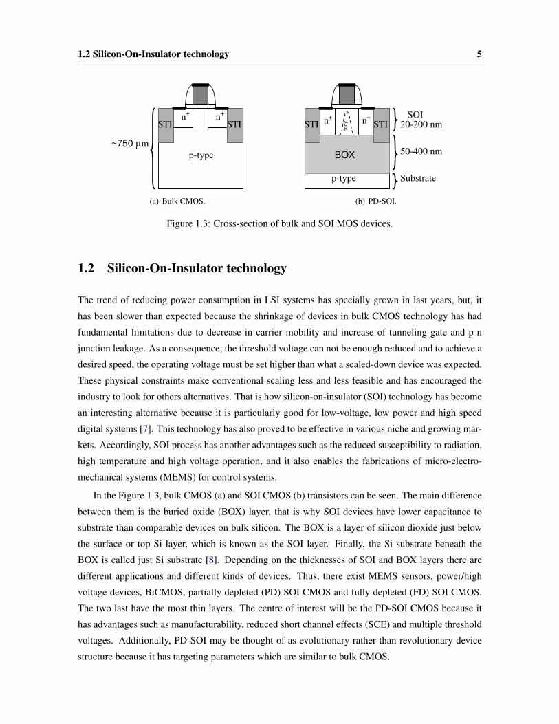
1.2 Silicon-On-Insulator technology 5
n+
n+
p-type
STI STI
~750 µm
(a) Bulk CMOS.
n+ n+
p-type
STI STI
BOX
bo
dy
50-400 nm
SOI20-200 nm
Substrate
(b) PD-SOI.
Figure 1.3: Cross-section of bulk and SOI MOS devices.
1.2 Silicon-On-Insulator technology
The trend of reducing power consumption in LSI systems has specially grown in last years, but, it
has been slower than expected because the shrinkage of devices in bulk CMOS technology has had
fundamental limitations due to decrease in carrier mobility and increase of tunneling gate and p-n
junction leakage. As a consequence, the threshold voltage can not be enough reduced and to achieve a
desired speed, the operating voltage must be set higher than what a scaled-down device was expected.
These physical constraints make conventional scaling less and less feasible and has encouraged the
industry to look for others alternatives. That is how silicon-on-insulator (SOI) technology has become
an interesting alternative because it is particularly good for low-voltage, low power and high speed
digital systems [7]. This technology has also proved to be effective in various niche and growing mar-
kets. Accordingly, SOI process has another advantages such as the reduced susceptibility to radiation,
high temperature and high voltage operation, and it also enables the fabrications of micro-electro-
mechanical systems (MEMS) for control systems.
In the Figure 1.3, bulk CMOS (a) and SOI CMOS (b) transistors can be seen. The main difference
between them is the buried oxide (BOX) layer, that is why SOI devices have lower capacitance to
substrate than comparable devices on bulk silicon. The BOX is a layer of silicon dioxide just below
the surface or top Si layer, which is known as the SOI layer. Finally, the Si substrate beneath the
BOX is called just Si substrate [8]. Depending on the thicknesses of SOI and BOX layers there are
different applications and different kinds of devices. Thus, there exist MEMS sensors, power/high
voltage devices, BiCMOS, partially depleted (PD) SOI CMOS and fully depleted (FD) SOI CMOS.
The two last have the most thin layers. The centre of interest will be the PD-SOI CMOS because it
has advantages such as manufacturability, reduced short channel effects (SCE) and multiple threshold
voltages. Additionally, PD-SOI may be thought of as evolutionary rather than revolutionary device
structure because it has targeting parameters which are similar to bulk CMOS.

6 Introduction
The PD-SOI has particular characteristics that influence in the devices operation. The SOI body,
which refers to the part of SOI layer that constitutes the body of MOSFET, is called floating body
(FB) because when the depletion region is formed, it does not reach the bottom part of top Si layer.
FB originates different phenomenons that should be studied in order to have a good understanding of
technology. Below, these effects are reviewed along with others related to process.
1.2.1 SOI MOSFET’s junction diode
PD-SOI MOSFET has two junction diodes identical in concept to those in the bulk device: the body-
source diode is often weakly reverse biased and the drain-body diode is usually reverse biased. The
body-source diode is a determinant mechanism in moving charge out of isolated body due to its biasing
conditions and it is known as diode action. Nonetheless, there are other effects from the SOI diodes
which are junction capacitances and junction leakages.
The junction capacitances are dependent on biasing conditions and they can be an important in-
fluence on SOI MOSFET behavior because in some cases, they have the ability to couple changes
in gate, source, or drain potential into the body’s voltage instantaneously. Junction leakage arises
form three major mechanisms which are the electron/hole recombination in the space charge region,
defects/impurities in the space charge region which disrupt the diode doping gradient from n-type to p-
type and high energy carriers which exceed the diode’s electronic barrier height. In bulk technologies,
the connection of substrate or N-well to supply rail and the source or drain node driven by preceding
circuitry on a second terminal, uphold the junction leakage. However, in the PD-SOI devices, junction
leakage directly affects body potential due to its floating nature and thus it affects the performance,
over an extended period. The junction current are widely influenced by the operation conditions due to
its dependence on voltage and temperature, as represented simplistically in the classic diode equation.
1.2.2 Impact Ionization
SOI technology presents the problem of impact ionization and it continues to cause long-term wear
out, but also has more immediate effect on the device’s performance. Majority carriers have the ability
to induce damage in the host FET structure when they are excited by high electric fields. The damage
is accumulative and it modifies the threshold voltage of NFET and PFET devices. As consequence,
the drain current is reduced in NFETs and increased in PFETs, which affects the performance and can
eventually cause failures.
The are three mechanisms which induce degradation by hot carrier: conducting hot-carrier, non-
conducting hot-carrier and substrate hot-carrier. In SOI, the first two are predominant. Conducting
hot-carrier degradation occurs as the device is turned on. At pinch-off voltage, the electric field across
the excessively short uninverted remainder of channel is then extremely high and essentially ’heats’
1.2 Silicon-On-Insulator technology 7
the electrons to an effective high temperature. The kinetic energy originated by the above mentioned
makes some electrons in the case of NFETs not to be collected by the drain and the carriers energy
will be injected into the insulator. In addition to the damage at silicon interface, impact ionization
of silicon lattice atoms leaves behind positive charge, which accumulates in the isolated body of the
device.
The nonconducting hot carrier degradation occurs in a similar way but when the gate voltage is less
than VT . Here, a portion of the inverted carriers present in subthreshold or punchtroungh current has
sufficient energy to produce damage in the FET gate insulator oxide. The substrate hot electron effects
are absent for the most part in SOI. The first two modes mentioned originated a charge accumulation
in the body region which is significant in SOI due to FB.
1.2.3 Floating body effects
History effect and threshold voltage variability
The electrical property that largely determines the behaviour of a PD-SOI device is history effect. This
makes the I-V characteristic not to be constant because it depends on charge of the body. This charge
and its distribution caused by gate, source and drain potentials widely affect the device performance.
Charge in the body is directly related to the potential of body. Due to the body bias the junctions are
reverse-biased which must be overcome by gate drives. It can be seen as a modification in the threshold
voltage. The changes in charge contained in the body are associated to a number of factors among
them the previous state of transistor, the schematic position of transistor, slewing of the input and the
load capacitance, channel length and PVT variations, junction temperature and operating frequency,
and specific switch factor.
There are different paths to convey charge into and out of the body. Three paths move charges into
the body which are usually slow and they are related to impact ionization and the junction leakage
across the drain-body or source-body diode. However, there are only two paths that move charges out
of the body that can be fast, and they are related to forward-biases of junction diodes. These transport
mechanisms of charge affect the dynamic behaviour of the device and they can originate an effect
named kink which consist in the increment of IDS by decreasing of threshold voltage. It occurs when
suddenly, a considerable amount of positive charge is injected into the body.
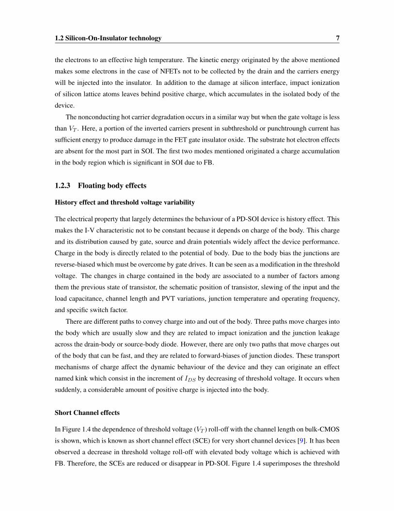
Short Channel effects
In Figure 1.4 the dependence of threshold voltage (VT ) roll-off with the channel length on bulk-CMOS
is shown, which is known as short channel effect (SCE) for very short channel devices [9]. It has been
observed a decrease in threshold voltage roll-off with elevated body voltage which is achieved with
FB. Therefore, the SCEs are reduced or disappear in PD-SOI. Figure 1.4 superimposes the threshold

8 Introduction
Th
resh
old
Vo
ltag
e (V
)
SOI Device, High VTH
SOI Device, Low VTH
Bulk Device, Nominal VTH
Channel Length (µm)
Figure 1.4: Roll-off of threshold voltage with Leff for bulk and SOI devices [9].
voltage dependence on channel length for the SOI MOSFET for high and low threshold options. This
feature increases scalability and reduces variability of performance across the process window of
Leff .
For short-channel devices, Drain Induced Barrier Lowering (DIBL) is a prominent effect in MOS-
FET which changes with the introduction of FB. While in bulk-CMOS, due to drain voltage, the ef-
fective channel length is reduced by the expansion of space-charge depletion region in drain-to -body
junction, in PD-SOI device with FB, the channel length remains long because the body bias makes
shrink the space region surrounding the drain. However, DIBL becomes artificially high due to strong
influence of body in the threshold voltage which is reduced by the injection of positive charge into
body through junction diodes. Depending on process, an SOI device with its body contact connected
to a stable potential will revert to the bulk-CMOS DIBL values.
Bipolar Device Action
In bulk CMOS effects like latch-up arise from the presence of parasitic bipolar junction transistor
(BJT). Devices in bulk-CMOS or PD-SOI form a bipolar structure where the drain acts as the BJT
collector, the body as the BJT base and the source as the BJT emitter. However, an SOI device
with FB merely makes the presence of the bipolar parasitics substantially more prominent. It occurs
because the body can rise sufficiently high in voltage with respect to the source or drain to forward bias
the respective junction diodes, permitting bipolar gain. If the body has been highly charged and the
source of device is suddenly drawn low during a switch, the body-source junction diode can become
instantaneously forward biased, and will conduct a current IB momentarily from body (base) to source
(emitter) until the charge in the body is enough discharged. At the same time, bipolar action cause a
current of β · IB to briefly pass from drain (collector) to source (emitter). Generally, the value of β
is low, but depending on the value of VDD, this bipolar gain can be higher than 1. It is important to
maintain low the bipolar current because it can discharge a given node which originates logical errors
in dynamic and pass-gate circuits.
1.3 State of the art for CT Σ∆ Modulators. 9
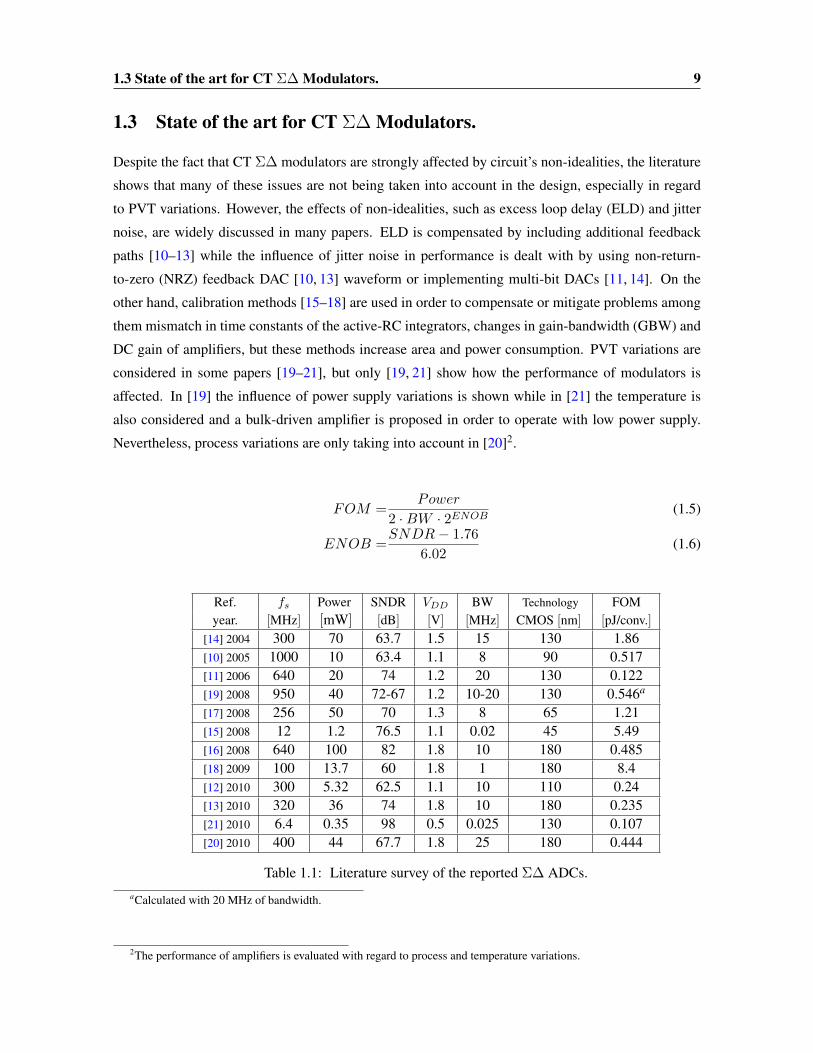
1.3 State of the art for CT Σ∆ Modulators.
Despite the fact that CT Σ∆ modulators are strongly affected by circuit’s non-idealities, the literature
shows that many of these issues are not being taken into account in the design, especially in regard
to PVT variations. However, the effects of non-idealities, such as excess loop delay (ELD) and jitter
noise, are widely discussed in many papers. ELD is compensated by including additional feedback
paths [10–13] while the influence of jitter noise in performance is dealt with by using non-return-
to-zero (NRZ) feedback DAC [10, 13] waveform or implementing multi-bit DACs [11, 14]. On the
other hand, calibration methods [15–18] are used in order to compensate or mitigate problems among
them mismatch in time constants of the active-RC integrators, changes in gain-bandwidth (GBW) and
DC gain of amplifiers, but these methods increase area and power consumption. PVT variations are
considered in some papers [19–21], but only [19, 21] show how the performance of modulators is
affected. In [19] the influence of power supply variations is shown while in [21] the temperature is
also considered and a bulk-driven amplifier is proposed in order to operate with low power supply.
Nevertheless, process variations are only taking into account in [20]2.
FOM =Power
2 ·BW · 2ENOB(1.5)
ENOB =SNDR− 1.76
6.02(1.6)
Ref. fs Power SNDR VDD BW Technology FOMyear. [MHz] [mW] [dB] [V] [MHz] CMOS [nm] [pJ/conv.]
[14] 2004 300 70 63.7 1.5 15 130 1.86[10] 2005 1000 10 63.4 1.1 8 90 0.517[11] 2006 640 20 74 1.2 20 130 0.122[19] 2008 950 40 72-67 1.2 10-20 130 0.546a
[17] 2008 256 50 70 1.3 8 65 1.21[15] 2008 12 1.2 76.5 1.1 0.02 45 5.49[16] 2008 640 100 82 1.8 10 180 0.485[18] 2009 100 13.7 60 1.8 1 180 8.4[12] 2010 300 5.32 62.5 1.1 10 110 0.24[13] 2010 320 36 74 1.8 10 180 0.235[21] 2010 6.4 0.35 98 0.5 0.025 130 0.107[20] 2010 400 44 67.7 1.8 25 180 0.444
Table 1.1: Literature survey of the reported Σ∆ ADCs.aCalculated with 20 MHz of bandwidth.
2The performance of amplifiers is evaluated with regard to process and temperature variations.

10 Introduction
In the Table 1.1 are listed the LP Σ∆ ADCs reported in last years. The main trend observed
is higher frequency operation with low OSR, which implies the use of multibit ADCs and DACs to
improve the power efficiency. However, there are works as [21] that has a low bandwidth with a
good figure of merit (FOM)(1.5) 3. The better FOM are achieved in pre or post-layouts simulations
[12, 13, 21] and [11] shows the best FOM reported with measurement results.
1.4 Dissertation Organization
This document is oriented to design a high DC amplifier on SOI CMOS technology that must be robust
to PVT variations in order to verify its performance in a CT Σ∆ modulator. This development is done
on this document by identifying how the modulator behaviour is affected by circuit’s non-idealities
and evaluating how to overcome this problems. To fully understand the procedure, below is shown the
organization of this document.
In chapter 2, a review of the modulator’s theory is done. Also, the effects of circuit’s non-idealities
is presented and how they can be included in the model of the modulator. In chapter 3, the design of
proposed circuits is performed, including the explanation of how to increase the gain of amplifiers and
finally, a comparison with a conventional amplifier. Chapter 4 shows simulations results of the CT
Σ∆ modulator using the proposed circuits. A brief comparison is done to see how the modulator is
affected by PVT variations in the used amplifiers. Finally, some conclusions and the future work are
drawn in chapter 5.
3ENOB refers to Effective Number of Bits

Chapter 2
Theory and modeling of CT Σ∆
modulators
2.1 Issues and Operation of the Modulator
In previous chapter, the basic theory of Σ∆ modulation in discrete time was explained; however, the
implementation of a modulator can be made in continuous time too. Figure 2.1 [3] shows an illustrative
schematic of a CT Σ∆ converter where the input signal can be subject to anti-aliasing filtering or
not. The loop filter H(s) now consists of CT filters, which can be active RC-filters using OpAmps,
operational transconductance amplifiers (OTA), gmC-filters or even LC-resonator structures. The
internal quantizer is a sampled or latched circuit, which is clocked at the sampling frequency fs of the
modulator. Below, the operation of these building blocks will be explained showing their differences
with the blocks that are used by its counterpart in DT.
Σ Η(s)
DAC
fs
u(t)
fs/2
xd(t) q(t) y(n)
y(t)
fb
yd(n)
Antialiasing filter
Σ∆ modulator Decimator
Digital filter
Down sampling
Figure 2.1: Block diagram of a CT Σ∆ A/D converter [3].

12 Theory and modeling of CT Σ∆ modulators
2.1.1 Sampling Operation
As the S/H circuit is placed at the input of the converter in DT modulators, every error of this block
is added to the input signal. In contrast, the sampling operation in CT modulators takes place inside
the Σ∆ loop, therefore, all non-idealities of the sampling process are subject to noise-shaping. It is
an interesting feature because S/H operation at high fs requires demanding specifications difficult to
achieve.
The implementation of the sampling operation inside modulator loop, after the loop filter, results
to some extent in implicit anti-aliasing filtering. This attribute can heavily reduce the required specifi-
cations of a front-end AAF and even makes it sometimes unnecessary. Mainly in high-speed circuits
or architectures with very low oversampling ratios, this can be an strong argument to choose a CT Σ∆
implementation.
Timing errors of the sampling clock, such as jitter, have a significant impact on the DT modulator
sampling operation. The S/H circuit can sample the input at a wrong time instant, which produces an
equivalent amplitude error that degrades the SNR of the converter. Thus, the front-end S/H sets an
upper limit on the performance of the entire DT modulator. On the other hand, the noise-shaped S/H
errors in CT modulators make the sampling operation to be less sensitive to jittered clock. Nonetheless,
the CT modulator are very sensitive to timing variations or delays within the feedback path. This is
not an issue in DT modulators because the filters in SC circuits are usually designed as to safely settle
within half sampling period.
Implicit Anti-aliasing Filter
This feature is easily understood if the first-order modulator of figure 2.1 is considered (H(s) = I(s))
without additional AAF. The input to the quantizer at a sampling instant depends on the feedback sig-
nal and additionally on an integrated version of the input signal∫ (n+1)Ts
nTs
u(t)dt [3]. This integration
can be expressed by a convolution of the input signal with a rectangular window which is a multiplica-
tion in frequency domain between the input spectrum and a sinc(πf/fs)-function. This sinc-function
attenuates the signal spectrum exactly at multiples of the sampling frequency and therefore shows the
function of an AAF. Thus, it can be expected that higher order modulation and larger loop-gain results
in higher order anti-aliasing property.
The figure 2.2 shows the AAF of the input signal in a CT Σ∆ modulator. From this equivalent
model, the anti-aliasing filter can be approximately given by
FAAF (w) =FF (s = jw)
FF (z = ejwTs)(2.1)

2.1 Issues and Operation of the Modulator 13
FF(s)
fsu(t) y(n)FF(z)
u1(t)NTF2
AAF
Figure 2.2: Equivalent representation of a CT Σ∆ modulator considering its implicit AAF [3].
where FF (s) is the feed-forward filter of CT modulator and FF (z) its DT equivalent. From (2.1), it
can be seen that the AAF-behavior for different loop filter characteristics such as low-pass, band-pass,
all poles at DC or optimally spread inside the in-band is preserved.
2.1.2 Filter Realization
The loop filters in DT and CT modulators are integrators or resonators which are commonly imple-
mented with SC circuits and continuous-time integrators respectively. The signals in DT circuits are
quickly changing, therefore, the modulators employing the SC technique have a maximum clock rate,
which is limited by the OTA bandwidth and the need of several time constants to settle the charge
transfer with given accuracy. In contrast, in CT modulators all signals are continuous-time wave-
forms; thus the OpAmp speed restrictions are drastically relaxed, and CT modulators can be clocked
at higher frequencies that actually tend to lie between three and five times their DT counterparts.
Linearity behaviour concerning the virtual ground node is a matter of both DT and CT architec-
tures. Despite the fact that DT modulators have large glitches in this node due to the fast SC pulses,
its effects in linearity can be neglected as the signal of interest in DT is the finally settled value. In
the case of CT modulators, the virtual ground node can be kept quiet; characteristic that must be
permanently kept because the integration of a continuously changing waveform requires permanent
linearity . Another issue is the voltage dependency (nonlinearity) of the passive and active components
used. This imperfection leads to harmonic distortion at the modulator output, therefore, limiting the
performance of CT Σ∆ modulators due to nonlinearity of resistor and transconductances stages. In
particular, the first transconductor must have the overall accuracy of the system.
The transfer function of the loop filter is heavily affected by integrators implementation, i. e.,
the utilization of discrete or continuous-time circuits. The former implementation defines its gain by
capacitors ratio which is very precise since absolute mismatch of both capacitors does not affect the
integrator gain. In contrast, CT circuits define the integrator gain by a RC or gmC product; they both
are subject to large process dependent variations, originating strongly loss of performance or even
unstable system in worts cases.

14 Theory and modeling of CT Σ∆ modulators
2.1.3 Quantizer Implementation
A common characteristic in both DT and CT Σ∆ modulators is that all non-idealities of the quantiza-
tion process are suppressed by noise shaping. However, the decision time of the internal quantizer and
its signal dependent variation (metastability) have a significantly different influence: while the deci-
sion time in DT systems is subject to half of sampling period, a CT Σ∆ ideally needs infinitely fast
quantization because the result is needed instantaneously to generate the continuous-time feedback
signal. Thus, severe performance limitations can arise.
Generally, low resolution flash ADCs are used in CT Σ∆ modulators due to its high speed.
Nonetheless, the exponentially increasing number of comparators, if a higher resolution is desired
, essentially increases power and area consumption. Additionally, the capacitive load seen by the last
integrator in the loop filter increases; therefore, the drive capability is pretty demanded by this load,
increasing even more the power consumption.
In order to relax the requirements imposed by flash ADCs, other conversion methods have been
adopted , such as successive approximation and tracking as internal quantizers. Successive approxi-
mation quantizers offer significant reduction in the number of comparators to only one; however, this
conversion method requires higher sampling frequencies for wide bandwidths which increases the
power consumption. On the other hand, the tracking quantizer approach takes advantage of the fact
that in a multi-bit Σ∆ modulator the feedback signal is usually changing only by one LSB at every
sampling instant. Thus, full quantization range of the internal quantizer is not needed, but only the
decision at a certain interval within the full-scale range. But it is possible that two LSB steps occur
which makes necessary the use of more than one comparator. Despite improving the stability of the
modulator, it still has to be ensured that the input signal to the tracking ADC within the modulator loop
is not slewing too fast. Otherwise, the ADC loses the input signal and again the modulator becomes
unstable. Consequently, both techniques impose their own advantages and drawbacks.
2.1.4 Feedback Realization
In DT modulators, the feedback signal is applied by charging a capacitor to a reference voltage and
discharging it onto the integrating capacitance. In contrast, the analog continuous-time feedback wave-
form is integrated over time and thus the Σ∆ modulator is sensitive to every deviation from the ideal
waveform of the feedback signal, originating some severe non-idealities.
The feedback DAC waveforms more commonly used are shown in Figure 2.3. Their classification
is defined by how long they are presented during a sampling period. In general, these waveforms, can
be expressed by
r(α, β) =
1 αTs ≤ t < βTs, 0 ≤ αTs < βTs ≤ Ts0 otherwise.
(2.2)

2.1 Issues and Operation of the Modulator 15
Ts
1
1 - e-sTs
s
rNRZ(t)=1, 0 ≤ t < Ts
0, otherwise
RNRZ(s)=
(a) NRZ pulse.
Ts
1 1, 0 ≤ t < Ts/2
0, otherwise
1 - e-s/2Ts
s
rNRZ(t)=RNRZ(s)=
(b) RZ pulse.
Ts
1 1, Ts/2 ≤ t < Ts
0, otherwise
1 - e-s/2Ts
s
rNRZ(t)=RNRZ(s)= e
-s/2Ts
(c) HRZ pulse.
Figure 2.3: Feedback DAC waveforms.
where for a Non-Return-to-Zero (NRZ), a Return-to-Zero (RZ) and a Half-delayed Return-to-Zero
(HRZ) pulse, the function becomes r(0, 1), r(0, 0.5) and r(0.5, 1), respectively.
A rectangular DAC pulse is particularly advantageous because it can be generated by simply
switching current or voltage sources using the system’s clock. However, the rectangular feedback
realization is strongly affected by the purity of the sampling clock because unlike the ADC, the re-
sulting DAC errors are directly introduced into the modulator input. Clock jitter directly modulates
the ADC decision point as well as the rising and falling edges of the DAC. These issues modify the
quantity of the feedback signal, resulting in a statistical integration error and consequently in increased
noise. This issue has motivated to propose others feedback waveforms realizations but none of them
has become popular.

16 Theory and modeling of CT Σ∆ modulators
There exist other performance limitations, among them, the delay between DAC and quantizer
clock originated by the finite time of switching, non-linearity due to slew rate (SR) limitations and
mismatch in multi-bit DACs. In spite of this, there are compensation techniques for these issues
such as dynamic element matching (DEM) and data weighted averaging (DWA) [6]. However, These
techniques have limitations in themselves that can impact negatively the performance.
2.2 Modeling and Simulation at System Level
In order to have a better approximation in modeling of modulators, the most of the non-idealities
must be taken into account. Generally, the model of the circuit’s non-idealities can be done by using
MATLAB and Simulink, which is widely reported. As a consequence, with a correct behavioural
model is possible to find the specifications of the building blocks to achieve the required specifications.
Next, it will be described how it is done.
2.2.1 Considering the Effects of Gain and Finite Bandwidth
There are two main repercussions that are introduced by the gain and GBW. Due to the finite gain, the
integrator pole is shifted to a value that depends on the sampling frequency and DC gain of amplifier.
Consequently, the CT integrator transfer function can expressed as [22]:
ITFεA0=
fsA0
s(1 +A0) + fs=
αfss+ γ
(2.3)
α =A0
1 +A0, γ =
fs1 +A0
(2.4)
where A0 is the OpAmp’s DC gain, and α and γ represent the integrator gain error and the pole
displacement, respectively. The effect of finite gain can be evaluated by calculating the total in-band
quantization noise power (IBN) which, for an arbitrary order (M) single loop modulator, is given
by [22]:
IBN(A0,M) =∆2
12k21k
2q
·[
1
A2L0 OSR
+
M∑m=1
π2mM(M − 1)...(M −m+ 1)
(2m+ 1)OSR2m+1A2(L−m)0 m!
](2.5)
with kq the effective quantizer gain and k1 the feedback coefficient. For a third order modulator the
IBN can be approximated by
IBN(A0) ≈ ∆2
12k21k
2q
·[
π6
7OSR7+
3π4
5OSR5A20
](2.6)

2.2 Modeling and Simulation at System Level 17
−
+
R1
Rn
v1
vn
vout
C
Figure 2.4: OpAmp RC integrator with multiple inputs.
where it is possible to calculate a critical DC gain to minimize the additional noise caused by the
integrator leakage. However, if integrated distortion is considered, the required DC gain has to be
much higher [22]. For single loop modulators, the minimum gain required is less than in multi-loop
architectures.
In the case of GBW, the influence over modulator is studied by using the single pole approximation
of amplifier (2.7). Accordingly, and neglecting the effect of DC gain, the entire ITF under the influence
of finite GBW considering an integrator with multiple inputs (Figure 2.4), can be expressed as (2.8),
where GBW is given in radians per seconds and kj are the scaling coefficients of all input paths, which
are mapped into different integrator resistors [23].
A0 =A0
1 + spdom
(2.7)
ITFεGBW ≈kifss
GBWGBW+
∑nj=0 |kjfs|
sGBW+
∑nj=0 |kjfs|
+ 1. (2.8)
From (2.8), the induced errors of finite GBW can be seen as a gain error (GEj) and a parasitic pole
(ωj) defined by:
GEi =GBW
GBW +∑n
j=0 |kjfs|; ωj =
s
GBW +∑n
j=0 |kjfs|. (2.9)
An estimation of IBN as a function of GBW for single loop modulators is shown in (2.10). GBWi
denotes the gain-bandwidth product of the respective integrator and KQ is ∆2
12k21k2q
. It can be shown
that the required GBW is smaller than in the switched capacitor counterparts [22].The modeling of
gain and finite GBW is made by using transfer functions as shown in Figure 2.5.
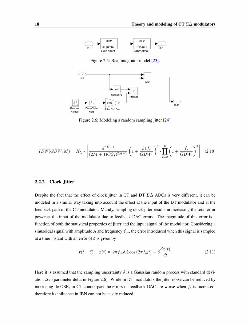
18 Theory and modeling of CT Σ∆ modulators
Out1
1
Gain effect
alfa2
s+gama2
GBW effect
GE2
1/w2s+1In1
1
Figure 2.5: Real integrator model [23].
Out1
1
Zero!Order
Hold
Random
Number
Product
Jitter Std. Dev.
delta
Derivative
du/dt
Add
In1
1
Figure 2.6: Modeling a random sampling jitter [24].
IBN(GBW,M) = KQ ·[
π2M−1
(2M + 1)OSR2M+1
(1 +
k1fsGBW1
)2
·M∏i=2
(1 +
fsGBWi
)2]
(2.10)
2.2.2 Clock Jitter
Despite the fact that the effect of clock jitter in CT and DT Σ∆ ADCs is very different, it can be
modeled in a similar way taking into account the effect at the input of the DT modulator and at the
feedback path of the CT modulator. Mainly, sampling clock jitter results in increasing the total error
power at the input of the modulator due to feedback DAC errors. The magnitude of this error is a
function of both the statistical properties of jitter and the input signal of the modulator. Considering a
sinusoidal signal with amplitude A and frequency fin, the error introduced when this signal is sampled
at a time instant with an error of δ is given by
x(t+ δ)− x(t) ≈ 2πfinδA cos (2πfint) = δdx(t)
dt. (2.11)
Here it is assumed that the sampling uncertainty δ is a Gaussian random process with standard devi-
ation ∆τ (parameter delta in Figure 2.6). While in DT modulators the jitter noise can be reduced by
increasing de OSR, in CT counterpart the errors of feedback DAC are worse when fs is increased,
therefore its influence in IBN can not be easily reduced.

2.2 Modeling and Simulation at System Level 19
Out1
1
Product Input!referred
third order
term
ki3
Input!referred
noise
Add
In1
1
Figure 2.7: Input-referred noise and distortion model [6].
2.2.3 Other Non-Indealities
Features such as noise and non-linearity of the amplifier are critical in the performance of a mod-
ulator. The additional noise can not be enough suppressed, therefore, the reduction of the SNR is
compromised. On the other hand, distortion directly affects the maximum achievable resolution by
degrading the SNDR. These issues can be modeled as in Figure 2.7 where white noise is equivalent to
thermal noise and the cubic power term followed by a gain stage is the harmonic distortion if a fully
differential implementation is accomplished. Other non-idealities such as saturation of amplifiers due
to power supply and excess loop delay (ELD) [3] can be included in the model by using saturation
blocks and continuous time processing delay, respectively.
2.2.4 Example of Modeling a Modulator
To have an intuitive understanding of modeling, for this example the system proposed in [13], shown in
Figure 2.8 is used. The method to obtain the modulator coefficients is as follow: firstly, the optimized
noise transfer function in discrete time is obtained by using a delta-sigma toolbox of Simulink [13].
In this step, it is necessary to know the specifications that are required which define the order of the
filter loop: OSR and, in this case, the local feedbacks for obtaining a pair of optimal complex zeros in
NTF. The resulting NTF is given by (2.14):
Figure 2.8: Third order modulator including ELD compensation [13].

20 Theory and modeling of CT Σ∆ modulators
k1 k2 k3 k4 kz kb1,3 kd9/4 3/8 3/4 3/4 9/80 9/4 9/8
Table 2.1: Coefficients of modulator.
NTF =NTF (order,OSR, zeroopt, Hinf ) (2.12)
=NTF (3, 16, 1, 4) (2.13)
NTF (z) =z3 − 2.977z2 + 2.977z − 1
z3 − 0.6323z2 + 0.3992z − 0.05593(2.14)
For including the ELD compensation, it is necessary to re-sample at Ts/2 (here, the sampling
frequency is normalized to 1) the loop filter obtained from (2.14). Next, the impulse invariant trans-
formation is applied to (2.16), accomplishing an equivalent transfer function in CT (2.17).
H(z) =1−NTF (z)
NTF (z)(2.15)
H(z1/2) = d2d(H(z)) (2.16)
H(s) = d2c(H(z1/2)) (2.17)
Finally, the NTF in CT is derived from (2.17). The relationship between coefficients of modulator
and (2.17) can be easily found after applying the Mason’s rule to 2.8 where (2.20) is obtained. The
coefficients are presented in Table 2.1.
NTF (s) =1
1 +H(s)(2.18)
NTF (s) =s3 + 0.02401s
s3 + 2.321s2 + 1.705s+ 0.6147(2.19)
NTF (s) =s3 + kzk3s
s3 + kb3s2 + (kzk3 + kb1k4)s+ kb1k2k3(2.20)
Simulation Results
There are some considerations that must be taken into account to have accurate simulation results.
First, the algorithm used for calculating the Power Spectral Density (PSD) is the Fast Fourier Trans-
2.2 Modeling and Simulation at System Level 21
Transport
Delay
To Workspace
y1
Sine Wave1
Scope4
Scope3
Scope2
Scope1
Scope
Saturation
REAL_INT3
In1Out1
REAL_INT2
In1Out1
REAL_INT1
In1Out1
Quantizer
Product2Product1
Product
Power Spectral Density
PSD
Noise_IM3_3
In1Out1
Noise_IM3_2
In1Out1
Noise_IM3_1
In1Out1
MJitter
In1Out1
Gain9
Fs
Gain8
Fs
Gain7
kz
Gain6
Fs
Gain5
k1
Gain4
k4
Gain3
k2
Gain2!K!
Gain10
k3
Gain1!K! Gainkd
Constant
!C!
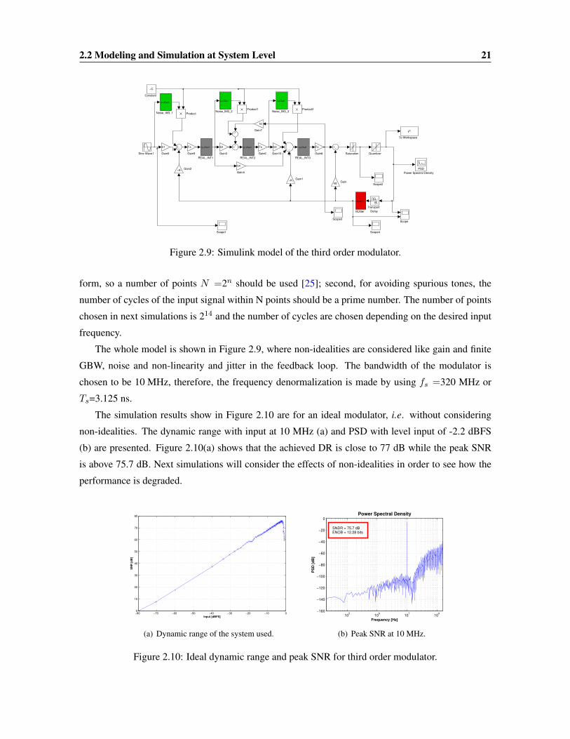
Figure 2.9: Simulink model of the third order modulator.
form, so a number of points N =2n should be used [25]; second, for avoiding spurious tones, the
number of cycles of the input signal within N points should be a prime number. The number of points
chosen in next simulations is 214 and the number of cycles are chosen depending on the desired input
frequency.
The whole model is shown in Figure 2.9, where non-idealities are considered like gain and finite
GBW, noise and non-linearity and jitter in the feedback loop. The bandwidth of the modulator is
chosen to be 10 MHz, therefore, the frequency denormalization is made by using fs =320 MHz or
Ts=3.125 ns.
The simulation results show in Figure 2.10 are for an ideal modulator, i.e. without considering
non-idealities. The dynamic range with input at 10 MHz (a) and PSD with level input of -2.2 dBFS
(b) are presented. Figure 2.10(a) shows that the achieved DR is close to 77 dB while the peak SNR
is above 75.7 dB. Next simulations will consider the effects of non-idealities in order to see how the
performance is degraded.
−80 −70 −60 −50 −40 −30 −20 −10 00
10
20
30
40
50
60
70
80
Input [dBFS]
SN
R [
dB
]
(a) Dynamic range of the system used.
105
106
107
108
−160
−140
−120
−100
−80
−60
−40
−20
0
SNDR = 75.7 dB
ENOB = 12.28 bits
Power Spectral Density
Frequency [Hz]
PS
D [
dB
]
(b) Peak SNR at 10 MHz.
Figure 2.10: Ideal dynamic range and peak SNR for third order modulator.

22 Theory and modeling of CT Σ∆ modulators
105
106
107
108
−160
−140
−120
−100
−80
−60
−40
−20
0
SNDR = 66.9 dB
ENOB = 10.82 bits
Power Spectral Density
Frequency [Hz]
PS
D [
dB
]
(a) First integrator noise. HD3=-56 dB.
105
106
107
108
−160
−140
−120
−100
−80
−60
−40
−20
0
SNDR = 70.8 dB
ENOB = 11.46 bits
Power Spectral Density
Frequency [Hz]
PS
D [
dB
]
(b) Second and third integrator noise. HD3=-56 dB.
Figure 2.11: Effect of white noise added to integrators for third order modulator.
105
106
107
108
−160
−140
−120
−100
−80
−60
−40
−20
0
SNDR = 72.5 dB
ENOB = 11.75 bits
Power Spectral Density
Frequency [Hz]
PS
D [
dB
]
(a) First integrator non-linearity.HD3=-50 dB without including noise.
105
106
107
108
−160
−140
−120
−100
−80
−60
−40
−20
0
SNDR = 73.5 dB
ENOB = 11.92 bits
Power Spectral Density
Frequency [Hz]
PS
D [
dB
]
(b) Second and third integrator non-linearity.HD3=-50 dB without including noise.
Figure 2.12: Influence of harmonic distortion of amplifiers for third order modulator.
105
106
107
108
−160
−140
−120
−100
−80
−60
−40
−20
0
SNDR = 72.3 dB
ENOB = 11.71 bits
Power Spectral Density
Frequency [Hz]
PS
D [
dB
]
(a) Effect of parasitic poles. Amplifiers gain Gain50 dB and GBW 800MHz.
105
106
107
108
−160
−140
−120
−100
−80
−60
−40
−20
0
SNDR = 75.7 dB
ENOB = 12.28 bits
Power Spectral Density
Frequency [Hz]
PS
D [
dB
]
(b) Ideal spectrum.
Figure 2.13: Considering the effect of GBW and finite gain for third order modulator.
2.2 Modeling and Simulation at System Level 23
105
106
107
108
−160
−140
−120
−100
−80
−60
−40
−20
0
SNDR = 73.3 dB
ENOB = 11.89 bits
Power Spectral Density
Frequency [Hz]
PS
D [
dB
]
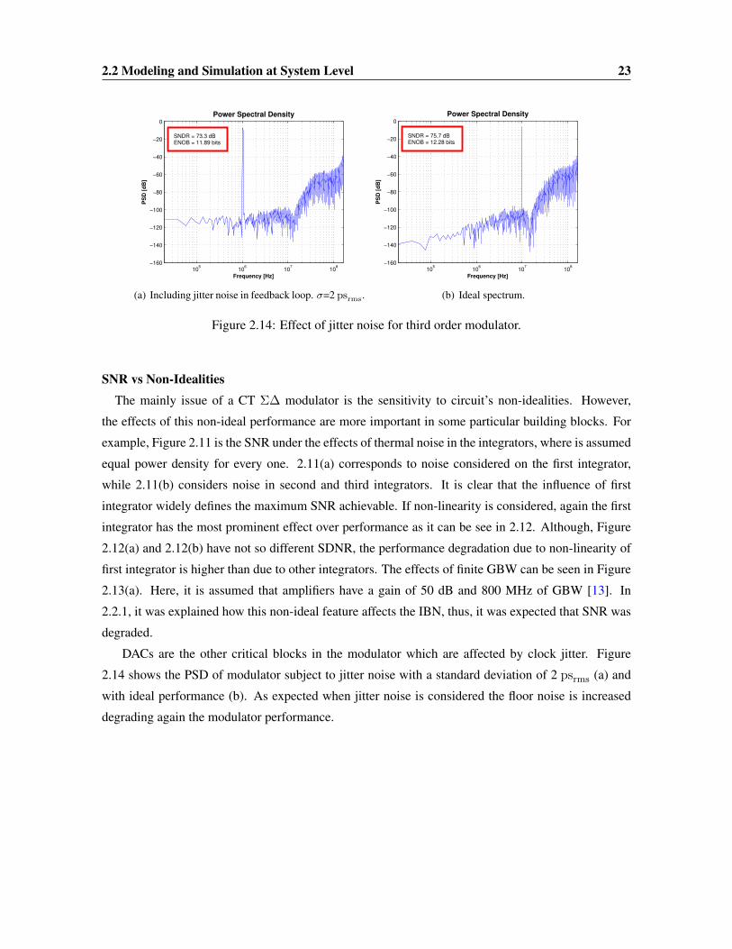
(a) Including jitter noise in feedback loop. σ=2 psrms.
105
106
107
108
−160
−140
−120
−100
−80
−60
−40
−20
0
SNDR = 75.7 dB
ENOB = 12.28 bits
Power Spectral Density
Frequency [Hz]
PS
D [
dB
]
(b) Ideal spectrum.
Figure 2.14: Effect of jitter noise for third order modulator.
SNR vs Non-IdealitiesThe mainly issue of a CT Σ∆ modulator is the sensitivity to circuit’s non-idealities. However,
the effects of this non-ideal performance are more important in some particular building blocks. For
example, Figure 2.11 is the SNR under the effects of thermal noise in the integrators, where is assumed
equal power density for every one. 2.11(a) corresponds to noise considered on the first integrator,
while 2.11(b) considers noise in second and third integrators. It is clear that the influence of first
integrator widely defines the maximum SNR achievable. If non-linearity is considered, again the first
integrator has the most prominent effect over performance as it can be see in 2.12. Although, Figure
2.12(a) and 2.12(b) have not so different SDNR, the performance degradation due to non-linearity of
first integrator is higher than due to other integrators. The effects of finite GBW can be seen in Figure
2.13(a). Here, it is assumed that amplifiers have a gain of 50 dB and 800 MHz of GBW [13]. In
2.2.1, it was explained how this non-ideal feature affects the IBN, thus, it was expected that SNR was
degraded.
DACs are the other critical blocks in the modulator which are affected by clock jitter. Figure
2.14 shows the PSD of modulator subject to jitter noise with a standard deviation of 2 psrms (a) and
with ideal performance (b). As expected when jitter noise is considered the floor noise is increased
degrading again the modulator performance.
24 Theory and modeling of CT Σ∆ modulators
To Workspace1
yout1
Sine Wave
Input1
Scope7Scope5
Saturation2 Saturation1
REAL_INT2
In1 Out1
REAL_INT1
In1 Out1
Quantizer3
Noise_IM3_2
In1 Out1
Noise_IM3_1
In1 Out1
Gain8
Fs
Gain4
Fs
Gain3!K!
Gain2
!K!
Gain11
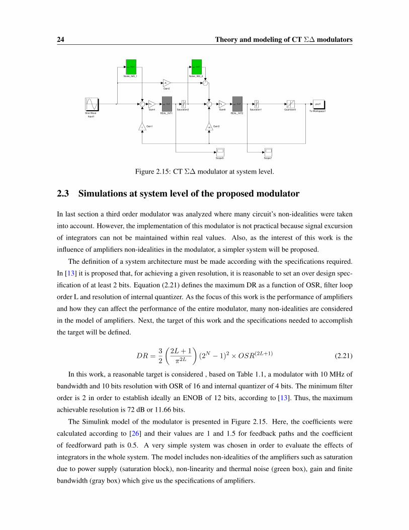
Figure 2.15: CT Σ∆ modulator at system level.
2.3 Simulations at system level of the proposed modulator
In last section a third order modulator was analyzed where many circuit’s non-idealities were taken
into account. However, the implementation of this modulator is not practical because signal excursion
of integrators can not be maintained within real values. Also, as the interest of this work is the
influence of amplifiers non-idealities in the modulator, a simpler system will be proposed.
The definition of a system architecture must be made according with the specifications required.
In [13] it is proposed that, for achieving a given resolution, it is reasonable to set an over design spec-
ification of at least 2 bits. Equation (2.21) defines the maximum DR as a function of OSR, filter loop
order L and resolution of internal quantizer. As the focus of this work is the performance of amplifiers
and how they can affect the performance of the entire modulator, many non-idealities are considered
in the model of amplifiers. Next, the target of this work and the specifications needed to accomplish
the target will be defined.
DR =3
2
(2L+ 1
π2L
)(2N − 1)2 ×OSR(2L+1) (2.21)
In this work, a reasonable target is considered , based on Table 1.1, a modulator with 10 MHz of
bandwidth and 10 bits resolution with OSR of 16 and internal quantizer of 4 bits. The minimum filter
order is 2 in order to establish ideally an ENOB of 12 bits, according to [13]. Thus, the maximum
achievable resolution is 72 dB or 11.66 bits.
The Simulink model of the modulator is presented in Figure 2.15. Here, the coefficients were
calculated according to [26] and their values are 1 and 1.5 for feedback paths and the coefficient
of feedforward path is 0.5. A very simple system was chosen in order to evaluate the effects of
integrators in the whole system. The model includes non-idealities of the amplifiers such as saturation
due to power supply (saturation block), non-linearity and thermal noise (green box), gain and finite
bandwidth (gray box) which give us the specifications of amplifiers.

2.3 Simulations at system level of the proposed modulator 25
−70 −60 −50 −40 −30 −20 −10 00
10
20
30
40
50
60
70
80
Input [dBFS]
SNR [dB]
(a) Dynamic range of the proposed modulator.
105
106
107
108
−160
−140
−120
−100
−80
−60
−40
−20
0
SNDR = 72.2 dB
ENOB = 11.70 bits
Power Spectral Density
Frequency [Hz]
PS
D [
dB
]
(b) SNDR at 1.5 MHz.
Figure 2.16: Ideal dynamic range and peak SNDR of proposed modulator.
In the Figure 2.16 the ideal performance of proposed modulator can be seen. Simulations were
made by considering a frequency input signal of 1.5 MHz and the obtained maximum stable amplitude
was -2 [dBFS]. DR range of the modulator is around 68 dB while the obtained peak SNR is 72.2 dB,
which is equivalent to have a ENOB of 11.7 bits. This results are very close to the estimated values
with numerical calculations.
To observe the influence of amplifier gain in the modulator, some simulations was made including
the DC gain and GBW model. In the Figure 2.17, the effect of gain variations are shown. Simulations
were made for different gain values from 60 dB to 44 dB where can be seen how the maximum
achievable SNR is degraded by reducing the amplifier gain. When DC gain is 60 dB, the peak SNR is
70 dB, but as the gain is reduced the maximum SNR falls close to 60 dB which gives a ENOB of 9.83.
As a result, the specification of 10 bits is not achieved which implies that is necessary to maintain a
gain in a safe margin to avoid an important degradation in modulator performance.
Figure 2.18 shows the DR and peak SNDR of the proposed system taking into account the non-
idealities mentioned. With input level of -2 dBFS, the maximum SNDR and DR achievable are 66 dB
and 67 dB respectively. The specification for amplifiers gain is based on (2.3) where, to have a pole
displacement 1 decade away from modulator bandwidth, it is required at least 50 dB. The GBW is set
at 2·fs. As the idea is to achieved 10 bits resolution, thermal noise and IM3 are set at values to maintain
a peak SNDR above 65 dB. The maximum thermal noise and IM3 to achieve the specifications above
mentioned are 31 nV/√
Hz and -62 dB, respectively.
The performance obtained with the model is considered enough to use this in the design at circuit
level. In the next chapter the design of amplifiers will be made based on specifications accomplished
with simulations at system level.

26 Theory and modeling of CT Σ∆ modulators
105
106
107
108
−160
−140
−120
−100
−80
−60
−40
−20
0
SNDR = 70.2 dB
ENOB = 11.36 bits
Power Spectral Density
Frequency [Hz]
PS
D [
dB
]
(a) Peak SNR considering amplifier gain of 60 dB.
105
106
107
108
−160
−140
−120
−100
−80
−60
−40
−20
0
SNDR = 69.3 dB
ENOB = 11.23 bits
Power Spectral Density
Frequency [Hz]
PS
D [
dB
]
(b) Peak SNR considering amplifier gain of 50 dB.
105
106
107
108
−160
−140
−120
−100
−80
−60
−40
−20
0
SNDR = 60.9 dB
ENOB = 9.83 bits
Power Spectral Density
Frequency [Hz]
PS
D [
dB
]
(c) Peak SNR considering amplifier gain of 44 dB.
Figure 2.17: Amplifier gain effect in the performance of the proposed modulator.
−70 −60 −50 −40 −30 −20 −10 00
10
20
30
40
50
60
70
Input [dBFS]
SNR
SNDR
(a) Dynamic range of proposed modulator.
105
106
107
108
−160
−140
−120
−100
−80
−60
−40
−20
0
SNDR = 66.1 dB
ENOB = 10.69 bits
Power Spectral Density
Frequency [Hz]
PS
D [
dB
]
(b) SNDR at 1.5 MHz.
Figure 2.18: Dynamic range and peak SNDR including amplifier’s non-idealities in the proposedmodulator.

Chapter 3
Design and Simulations of the ProposedCircuits
In the last chapter, the main building blocks of a CT Σ∆ modulator and their principle of operation and
more relevant issues were presented. An important conclusion is that the modulator is very sensitive
to circuit’s non-idealities unlike its counterpart in DT. The non-ideal performance of filter loop, i.e.
the integrators, can significantly impact the specifications achievable with a modulator by increasing
the IBN or even causing unstable operation. These drawbacks are mainly due to mismatch in filter
coefficients (RC products) and the variations of DC gain and GBW of OpAmp. While calibration
methods are widely used to overcome mismatch in RC products, compensating or mitigating PVT
variations in OpAmps is a more difficult task. This chapter will focus in proposing an OpAmp that
reduces PTV variations while providing high DC gain. The design of the circuits will be made on SOI
CMOS 45 nm technology.
3.1 Gain-Enhancement
In section 2.3 the required specifications for the amplifiers were presented. It was found that the
minimun gain and GBW must be 50 dB and 640 MHz, respectively. As first consideration, implemen-
tation of fully differential amplifiers will be made in order to reduce distortion and its characteristic of
noise rejection [27]. Secondly, the technology used has not problem with GBW specification because
of the high cutoff frequency (ft) of its transistors. On the other hand, to achieve gain specification is a
challenging task due to SCE and reduction of power supply. Below, a possible solution to the problem
was briefly explained.
In the literature, there are many techniques used to improve DC gain of amplifiers. A commonly
used technique is cascode transistors but it is not longer available in scaled technologies due to the
restrictions in voltage supply. Instead cascode, cascade is an available alternative which has the draw-

28 Design and Simulations of the Proposed Circuits
X
M1
M2
W L
mW L
W (m+1)L
Figure 3.1: Self-cascode transistor.
RzRz
CcCc
M1 M2
M3 M4
Mc1 Mc2Vcm
Vinp Vinn
Voutn Voutp
Figure 3.2: Two stage Miller amplifier.
back of making more difficult the frequency compensation. So, to improve DC gain without using
many cascade stage, a possible solution is used self-cascode transistors (Figure 3.1) which can be seen
as a single transistor with a higher output impedance. This can be explained considering that M1 ope-
rates in saturation region while M2 operates in linear region. Thus, transconductance of M1 is given
by (3.1) where VGX can be approximated to VGS2 due to VDS2 is low. Thus, gds2 can be calculated
as in (3.2). The equivalent gds (3.3) and gm (3.4) correspond to a transistor with channel length of
(m+ 1) times the M1 channel length, therefore achieving a high output impedance.
gm1 =µCoxW1
L1(VGX − VTH) (3.1)
gds2 ≈gm1
m(3.2)
gds,eq ≈gds1
(m+ 1)(3.3)
gm,eq ≈gm1
(m+ 1)(3.4)

3.1 Gain-Enhancement 29
1:k
vinp
voutngm
1:1
+-
-+
vinn
voutp
1:1
1:k
k:1
k:1
Figure 3.3: Amplifier with bidirectional output drive.
Vin
Vout
M1
M2 M3
VDD
V1
Figure 3.4: Current shunt.
Self-cascode transistor can be used in a two stage miller amplifier (Figure 3.2), which is a very
common circuit. Despite improving output impedance, the amplifier gain is still limited beside being
a sensitive circuit to PVT variations. So, the main idea will be reduced this sensitivity while maintain
a relatively high DC gain.
As an alternative can be used a current mirror amplifier with bidirectional output drive (Figure
3.3 [27]) which is expected that has a better behaviour than miller amplifier with regard to PTV
variation because its output is driven by the input transconductance stage (NMOS transistor) and
current mirror 1:1 PMOS which are added to the output. However, this amplifier has only a gain stage
making necessary to improve its gain beside using self-cascode transistors.
[28] proposes an enhanced current mirror amplifier by current shunt. This can be understood
analyzing Figure 3.4. Generally, the gain of this stage is given by (3.5) which can be increased by
making gm2 smaller than gm1 (3.6). This can be achieved as the most M1 current flow through M3.
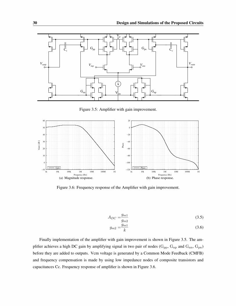
30 Design and Simulations of the Proposed Circuits
Vp
GpnGpp
Gnn GnpVcm
CcCc
Vinp VinnVoutp Voutn
Figure 3.5: Amplifier with gain improvement.
−10
0
10
20
30
40
50
60
1k 10k 100k 1M 10M 100M 1G
Gai
n [
dB
]
Frequency [Hz]
Gain
(a) Magnitude response.
−120
−100
−80
−60
−40
−20
0
20
1k 10k 100k 1M 10M 100M 1G
Ph
ase
Frequency [Hz]
Phase
(b) Phase response.
Figure 3.6: Frequency response of the Amplifier with gain improvement.
ADC =gm1
gm2(3.5)
gm2 =gm1
k(3.6)
Finally implementation of the amplifier with gain improvement is shown in Figure 3.5. The am-
plifier achieves a high DC gain by amplifying signal in two pair of nodes (Gpp, Gnp and Gnn, Gpn)
before they are added to outputs. Vcm voltage is generated by a Common Mode Feedback (CMFB)
and frequency compensation is made by using low impedance nodes of composite transistors and
capacitances Cc. Frequency response of amplifier is shown in Figure 3.6.

3.2 Final implementation of the amplifier 31
1:1
vin
vout
gm1 gm2
gm3
g1
1:1
1:1
1:1
+
-
v1+
-
+
-
-
-
+
+
-
+
go
Figure 3.7: Block diagram of OTA.
From Figure 3.6, it can be seen that gain is over 50 dB and its GBW is close to 650 MHz with a
PM over 80. However, it can be observed an unusual characteristic that is not presented in CMOS
technologies. The amplifier has a midband gain because transistors have zeros and poles at low fre-
quency. The number of poles and zeros is equal but the poles have major cutoff frequency than zeros
which results in gain attenuation as well as a phase increment at low frequency. These issues can
affect directly of the performance of modulator causing distortion because the DC gain of amplifiers
defines the noise shaping characteristic. It will be observed by simulating the whole system.
Despite having achieved the needed specifications, the amplifier has many problems in controlling
its common mode which causes its gain to have wide changes with PVT variations. In order to solve
this problem, in next section another amplifier finally will be proposed that is used in the whole system
implementation.
3.2 Final implementation of the amplifier
In Figure 3.7 the amplification scheme is shown conceptually. Supposing that the output transcon-
ductance of the first stage is g1, v1 voltage can be calculated by Vingm1
g1. Assuming go is the output
transconductance, vout is given by (gm2+gm3)v1go
. Thus, the overall gain is as follows
ADC =voutvin
=gm1(gm2 + gm3)
g1go. (3.7)
If gm2 = gm3 the gain is improved by a factor of two or 6 dB in comparison to amplifiers of two
stages. As current mirrors add only non-dominant poles, the amplifier can be seen as a two stage
amplifier with gain enhancement. This characteristic makes available miller frequency compensation,
which is a very common technique. So, the design of the amplifier is very simple. Below, it will be
explained how this scheme can be implemented at circuit level.

32 Design and Simulations of the Proposed Circuits
Vcm Cc1 Cc1
Rz Rz
CcCc
sn2sn1
sn2 sn1
M1
M3
Vinp Vinn Voutn Voutp
M4
M2
M5 M6
M7
Mc1
M8
Mc2Mc3 Mc4
Mc10Mc8Mc7Mc9
Figure 3.8: Enhanced amplifier with gain improvement.
3.2.1 Circuit implementation of proposed topology
In Figure 3.8 the OTA at circuit level is presented whose gain is given by (3.8). Some considerations
were take into account in order to obtain an amplifier with high gain and reduced PVT variations.
Firstly, the use of differential stage whenever it is possible since tail current avoids wide changes in
transconductance of transistors. In spite of the fact that M5,6 are grounded transconductors, the CMFB
circuit acts over them by adjusting the output node of the first transconductance stage through Vcm,
voltage which reduces wide variations of their transconductance. Finally, the signal flow of overall
transconductance to the output depends on PMOS and NMOS transconductance, so it is expected that
variations of transconductance at the output, with process variations, can be compensated or reduced
mainly in crossed process corners.
ADC =gm1,2(gm5,6 + gm7,8)
gout1gout(3.8)
Composite transistors are used in current mirrors in order to improve the output impedance. Miller
compensation with nulling resistor is applied to maintain a safe PM. However, the use of composite
transistors make additional compensation to be necessary to ensure an appropriate phase margin. Thus,
additional capacitance Cc1 is added between the output adn the low impedance node of transistors
Mc1,c2. Below, a comparison will be made between the amplifier proposed in this section and the two
stage Miller amplifier.

3.2 Final implementation of the amplifier 33
VREF
VOUTN
VOUTP
VCM
Figure 3.9: CMFB circuit.
Variable Value [µm] M
W1,2 3.2 -W3,4 9.6 -W5,6 3.6 -W7,8 4 -Wc1,2 7.2 3Wc3,4 7.2 3Wc7,8 4.8 3Wc9,10 4.8 3
Table 3.1: Dimensions of enhanced amplifier.
Variable Value [µm] M
W1,2 2.8 -W3,4 4 -Wc1,2 14.4 3Wtail 43 3Woutput 43 3
Table 3.2: Dimensions of Miller amplifier.
3.2.2 Design and simulations
To do the comparison, the CMFB circuit used for Miller amplifier and enhanced amplifier is the same
and is shown in Figure 3.9. CMFB circuit has two resistors to obtain the output common mode voltage
by averaging the differential outputs. Then, it compares the common mode voltage with a reference
voltage which originates a current unbalance that finally is feedback through VCM voltage.
To design both circuits a channel length of 200 nm will be used because it has an appropriate
trade off between ft of transistors and DC gain. The first amplifier of the system used a buffer which
can include excess phase. Thus, an over specification in PM is considered in order to maintain a
safe margin. For enhanced amplifier, a transconductance of 1 mA/V is required to achieve GBW
specification considering a load capacitance CL=200 fF and a compensation capacitance Cc=200 fF.
Fixing transconductances of M5,6 and M7,8 at 500 µA/V, to ensure a PM over 70, the zero nulling
resistor must be approximately 3 kΩ. To reduce distortion, transistors M1,2, M5,6 and M7,8 are biased
with an overdrive voltage of 150 mV. The resulting biasing current for the first transconductance stage
is 240 µA while for second transconductance stage (M7,8) is 120 µA. Biasing current of M5,6 is the
same as M7,8 as they have the same transconductance. As the current mirrors are implemented with
composite transistors, the m factor [29] is chosen 3 which gives an output impedance high enough for
the required gain. By using, voltage supply of 1.3 V the resulting power consumption is 1.25 mW.

34 Design and Simulations of the Proposed Circuits
−10
0
10
20
30
40
50
60
1k 10k 100k 1M 10M 100M 1G
Gai
n [
dB
]
Frequency [Hz]
V(outp,outn)
(a) Typical case magnitude response.
−120
−100
−80
−60
−40
−20
0
20
1k 10k 100k 1M 10M 100M 1G
Phas
e
Frequency [Hz]
Phase
(b) Typical case phase response
0
0.2
0.4
0.6
0.8
1
1.2
1.4
−30 −20 −10 0 10 20 30
Outp
ut
[V]
Vin [mV]
outpoutn
(c) Input DC sweep.
0.35
0.4
0.45
0.5
0.55
0.6
0.65
0.7
0.75
0.8
0.85
0.9
4 5 6 7 8
Outp
ut
[v]
t [us]
OutpOutn
(d) Typical case transient response
Figure 3.10: Performance of the enhanced amplifier : (a) and (b) show frequency response; (c) outputvoltage excursion; (d) transient response with output excursion of 500 mV.
Additional compensation capacitance Cc1 with value 200 fF is used to improve the PM. Table 3.1
shows a summary of dimensions.
In order to compare both amplifiers, the power consumption is restricted to be similar. For Miller
amplifier, the required transconductance of the first and second stage are 1 mA/V in order to achieve
a safe PM and the GBW specification. By using overdrive voltage of 150 mV the resulting biasing
current for the first stage is 240 µA while for each output branch it is 120 µA. The load capacitance
used is the same as the above design. The compensation capacitance needed is 300 fF and zero
nulling resistor is 1.2 kΩ. Transistor Mc1,2 are used with M=3 to improve output impedance the same
as current sources. By using the same voltage supply, the associated power consumption is 1.35 mW.
Table 3.2 summarizes the used dimensions.
Simulation results of the enhanced amplifier
The simulations were made by setting the device temperature to 60 C with power supply of 1.3 V
maintaining typical process. The performance of the amplifier can be summarized by figures showing
in 3.10. The maximum gain achieved is 53.7 dB while it has GBW of 575 MHz (Figures 3.10(a) and
3.10(b)) with PM of 75. Figure 3.10(c) shows the output dynamic range while 3.10(d) shows the
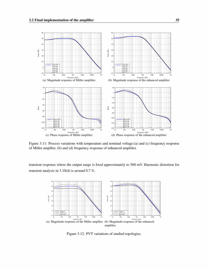
3.2 Final implementation of the amplifier 35
−10
0
10
20
30
40
50
60
1k 10k 100k 1M 10M 100M 1G
Gai
n [
dB
]
Frequency [Hz]
Gain TTGain FFGain SSGain FSGain SF
(a) Magnitude response of Miller amplifier.
−10
0
10
20
30
40
50
60
1k 10k 100k 1M 10M 100M 1G
Gai
n [
dB
]
Frequency [Hz]
Gain TTGain FFGain SSGain FSGain SF
(b) Magnitude response of the enhanced amplifier
−120
−100
−80
−60
−40
−20
0
20
1k 10k 100k 1M 10M 100M 1G
Ph
ase
Frequency [Hz]
Phase TTPhase FFPhase SSPhase FSPhase SF
(c) Phase response of Miller amplifier.
−140
−120
−100
−80
−60
−40
−20
0
20
1k 10k 100k 1M 10M 100M 1G
Ph
ase
Frequency [Hz]
Phase TTPhase FFPhase SSPhase FSPhase SF
(d) Phase response of the enhanced amplifier
Figure 3.11: Process variations with temperature and nominal voltage:(a) and (c) frequency responseof Miller amplfier, (b) and (d) frequency response of enhanced amplifier.
transient response where the output range is fixed approximately to 500 mV. Harmonic distortion for
transient analysis in 3.10(d) is around 0.7 %.
−10
0
10
20
30
40
50
60
1k 10k 100k 1M 10M 100M 1G
Gai
n [
dB
]
Frequency [Hz]
TypicalWorst caseBest case
(a) Magnitude response of the Miller amplfier.
−10
0
10
20
30
40
50
60
1k 10k 100k 1M 10M 100M 1G
Gai
n [
dB
]
Frequency [Hz]
TypicalWorst caseBest case
(b) Magnitude response of the enhancedamplifier.
Figure 3.12: PVT variations of studied topologies.

36 Design and Simulations of the Proposed Circuits
Specification Typ. Min. Max.
Gain 50.1 dB 45.7 dB 53.5 dBGBW 624 MHz 531 MHz 1.05 GHzPM 83 88.9 78.5
Table 3.3: Circuit specification of the Miller am-plifier
Specification Typ. Min. Max.
Gain 53.7 dB 51.9 dB 55.5 dBGBW 574 MHz 480 MHz 845 MHzPM 74.9 73.5 76.4
Table 3.4: Circuit specification of the enhancedamplifier.
3.3 Comparison of topologies
In this section, the studied topologies will be compared in order to evaluate how they are affected by
PVT variations. The specifications achieved with two stage Miller amplifier were ADC=50 dB with
GBW=624 MHz and PM=83. Harmonic distortion is less than 0.7 % for a output voltage excursion
of 500 mV. The comparison considers only the effects on midband gain and GBW of amplifiers.
3.3.1 Process variations
In Figure 3.11 the frequency response of OTA is shown considering only process variations. Simula-
tions were carried out by using power supply of 1.3 V and temperature of 60. Figures 3.11(a) and
3.11(c) show frequency response of the two stage Miller amplifier. The typical gain is 50 dB and its
maximal variations are from 48.9 dB to 50.9 dB which is equivalent to -14% and 9%, respectively.
The typical GBW is 624 MHz and it changes from 536 MHz to 733 MHz which is 15% and 17% . In
contrast, for the enhanced amplifier, the minimum and maximum gain are 53.1 dB and 53.9 dB which
in percentage is -7% and 2%. Its typical GBW is 574 MHz and it varies from 526.82 MHz (-8%) to
614 MHz (7%). The PM in proposed circuit varies 3 while in two stage Miller amplifier it changes
in 10.
3.3.2 Process, Voltage and Temperature Variations
Here, variations on voltage and temperature are also taken into account.A temperature range from
-20C to 100C and a voltage range ± 10% from nominal power supply is used. Figure 3.12 shows
typical, worst and best case of gain variations from topologies studied. In both amplifiers the worst
case is observed when PMOS and NMOS transistor have slow corner, -10% in power supply and
temperatures of 100C. The best case is when PMOS and NMOS transistor have fast corner, +10% in
power supply and temperatures of -20C. Figure 3.12 shows that enhanced amplifier has significantly
reduction in gain variations. For the worse case variations of GBW are not so different but for the best
case Miller amplifier has wide change. Maximal variations en GBW and DC gain of Miller amplifier
are 68% and 60%, while for proposed circuit are 47% and 23%. Harmonic distortion of the enhanced
amplifier in the worst case is 1.2 % while for Miller amplifier is 1.3 %. Tables 3.3 and 3.4 summarize
the comparison results with regard to DC gain, GBW and PM.

3.4 Loop Filter 37
R1 R2 C C1 RDAC1 RDAC2
3.125 KΩ 3.125KΩ 1 pF 0.5 pF 3.125KΩ 2 KΩ
Table 3.5: Resistor and capacitor values.
-
+ -
+-
+ -
+
C1
R1 R2
C C
C1 C C
R1 R2
Vinn
Vinp Voutn
Voutp
Figure 3.13: Loop filter.
3.4 Loop Filter
Figure 3.13 shows the implementation of the loop filter. Time constants of the integrators can be
calculated from (3.9) [3] where ki corresponds to filter coefficient and the product RiCi defines time
constant of the respective integrator. Resistance of DACs are computed in the same way. The feed-
forward coefficient is given by (3.10) [30]. By fixing integrator capacitors to 1 pF, the values of other
elements can be calculated. Table 3.5 show obtained values.
fs =1
CiRiki(3.9)
kfeedforward =C1
C(3.10)
A few number of papers mention the use of output buffers for amplifiers, i.e., they use OTA
as OpAmps in filter loops. However, the implementation of the loop filter with the enhanced OTA
shows that exits significant difference. Figure 3.14 shows the frequency response of the loop filter
using buffer (b) and without using buffer (a). Clearly, the time constants are affected by the output
impedance of amplifiers. The desired frequency response, with magnitude roll-off of 40 dB and phase
of 180, is not achieved without a buffer. The first amplifier has resistive load unlike the second
amplifier, therefore, it is necessary to use buffer a only in the first amplifier. In literature, an OTA
in open loop is sometimes used for the next integrators to avoid that first amplifier has resistive load.
Other implementations propose the use of a class AB output stage in order to drive the resistive load
of the first integrator [11]. In this work the use of a buffer which will be described below is proposed.
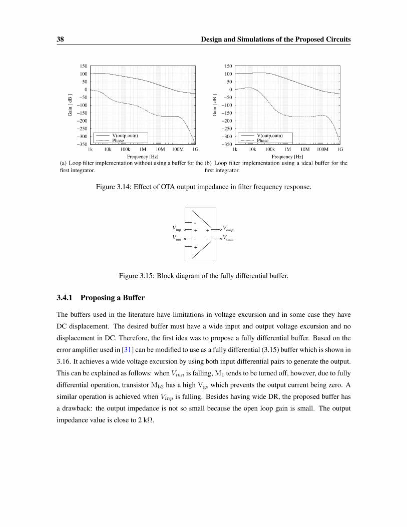
38 Design and Simulations of the Proposed Circuits
−350
−300
−250
−200
−150
−100
−50
0
50
100
150
1k 10k 100k 1M 10M 100M 1G
Gai
n [
dB
]
Frequency [Hz]
V(outp,outn)Phase
(a) Loop filter implementation without using a buffer for thefirst integrator.
−350
−300
−250
−200
−150
−100
−50
0
50
100
150
1k 10k 100k 1M 10M 100M 1G
Gai
n [
dB
]
Frequency [Hz]
V(outp,outn)Phase
(b) Loop filter implementation using a ideal buffer for thefirst integrator.
Figure 3.14: Effect of OTA output impedance in filter frequency response.
-
+
-
+
Vinn
Vinp
Voutn
Voutp
-
+
Figure 3.15: Block diagram of the fully differential buffer.
3.4.1 Proposing a Buffer
The buffers used in the literature have limitations in voltage excursion and in some case they have
DC displacement. The desired buffer must have a wide input and output voltage excursion and no
displacement in DC. Therefore, the first idea was to propose a fully differential buffer. Based on the
error amplifier used in [31] can be modified to use as a fully differential (3.15) buffer which is shown in
3.16. It achieves a wide voltage excursion by using both input differential pairs to generate the output.
This can be explained as follows: when Vinn is falling, M1 tends to be turned off, however, due to fully
differential operation, transistor Mb2 has a high Vgs which prevents the output current being zero. A
similar operation is achieved when Vinp is falling. Besides having wide DR, the proposed buffer has
a drawback: the output impedance is not so small because the open loop gain is small. The output
impedance value is close to 2 kΩ.
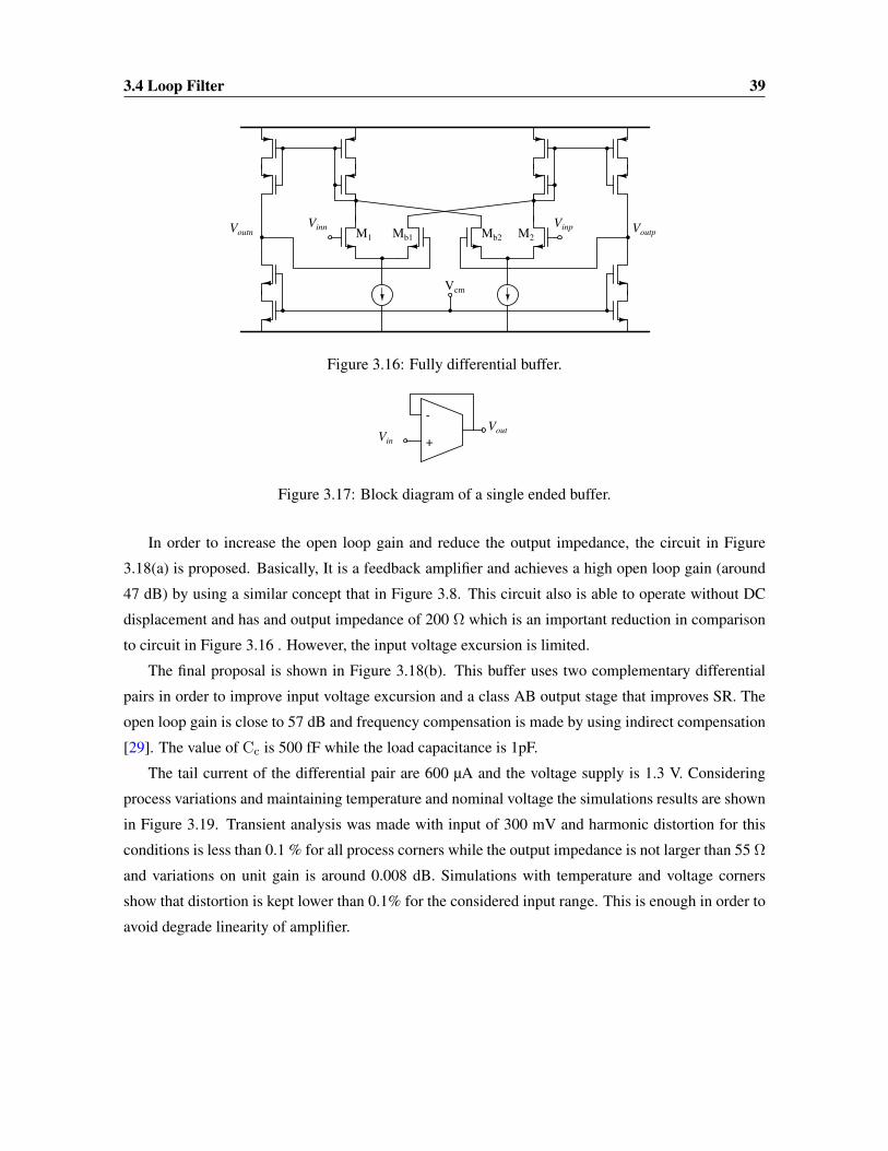
3.4 Loop Filter 39
M2M1 Mb1 Mb2
Vcm
Vinn VinpVoutn Voutp
Figure 3.16: Fully differential buffer.
-
+Vin
Vout
Figure 3.17: Block diagram of a single ended buffer.
In order to increase the open loop gain and reduce the output impedance, the circuit in Figure
3.18(a) is proposed. Basically, It is a feedback amplifier and achieves a high open loop gain (around
47 dB) by using a similar concept that in Figure 3.8. This circuit also is able to operate without DC
displacement and has and output impedance of 200 Ω which is an important reduction in comparison
to circuit in Figure 3.16 . However, the input voltage excursion is limited.
The final proposal is shown in Figure 3.18(b). This buffer uses two complementary differential
pairs in order to improve input voltage excursion and a class AB output stage that improves SR. The
open loop gain is close to 57 dB and frequency compensation is made by using indirect compensation
[29]. The value of Cc is 500 fF while the load capacitance is 1pF.
The tail current of the differential pair are 600 µA and the voltage supply is 1.3 V. Considering
process variations and maintaining temperature and nominal voltage the simulations results are shown
in Figure 3.19. Transient analysis was made with input of 300 mV and harmonic distortion for this
conditions is less than 0.1 % for all process corners while the output impedance is not larger than 55 Ω
and variations on unit gain is around 0.008 dB. Simulations with temperature and voltage corners
show that distortion is kept lower than 0.1% for the considered input range. This is enough in order to
avoid degrade linearity of amplifier.

40 Design and Simulations of the Proposed Circuits
Vin VoutVout
(a) Buffer with open loop gain improved
VDD
VinVout
Cc
Cc
Vout
(b) Buffer with input voltage excursionimproved
Figure 3.18: Single ended buffers.
In the next chapter, the simulations results of the whole system using the circuits designed in this
chapter will be presented . VerilogA will be used to model ADC and DACs. The influence due to PVT
variations in amplifiers over the modulator performance will be evaluated. It is expected to reduce the
performance degradation associated to the enhanced amplifier.
−2.5
−2
−1.5
−1
−0.5
0
1k 10k 100k 1M 10M 100M 1G
Gan
an
cia
[ d
B ]
Frecuencia [Hz]
TTFFSSFSSF
(a) Magnitude response.
0.3
0.4
0.5
0.6
0.7
0.8
0.9
1
200 300 400 500 600 700
Ou
tpu
t [V
]
t [ns]
TTFFSSFSSF
(b) Transient response with output voltage excursion of600 mV.
Figure 3.19: Process variations for proposed the buffer.
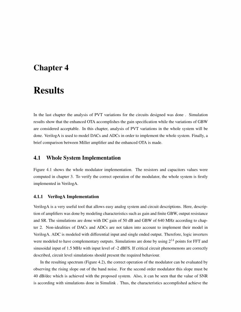
Chapter 4
Results
In the last chapter the analysis of PVT variations for the circuits designed was done . Simulation
results show that the enhanced OTA accomplishes the gain specification while the variations of GBW
are considered acceptable. In this chapter, analysis of PVT variations in the whole system will be
done. VerilogA is used to model DACs and ADCs in order to implement the whole system. Finally, a
brief comparison between Miller amplifier and the enhanced OTA is made.
4.1 Whole System Implementation
Figure 4.1 shows the whole modulator implementation. The resistors and capacitors values were
computed in chapter 3. To verify the correct operation of the modulator, the whole system is firstly
implemented in VerilogA.
4.1.1 VerilogA Implementation
VerilogA is a very useful tool that allows easy analog system and circuit descriptions. Here, descrip-
tion of amplifiers was done by modeling characteristics such as gain and finite GBW, output resistance
and SR. The simulations are done with DC gain of 50 dB and GBW of 640 MHz according to chap-
ter 2. Non-idealities of DACs and ADCs are not taken into account to implement their model in
VerilogA. ADC is modeled with differential input and single ended output. Therefore, logic inverters
were modeled to have complementary outputs. Simulations are done by using 214 points for FFT and
sinusoidal input of 1.5 MHz with input level of -2 dBFS. If critical circuit phenomenons are correctly
described, circuit level simulations should present the required behaviour.
In the resulting spectrum (Figure 4.2), the correct operation of the modulator can be evaluated by
observing the rising slope out of the band noise. For the second order modulator this slope must be
40 dB/dec which is achieved with the proposed system. Also, it can be seen that the value of SNR
is according with simulations done in Simulink . Thus, the characteristics accomplished achieve the

42 Results
-
+ -
+-
+ -
+
CC1
C1
R1 R2
+ + --
-
+
Buffer
C C
C
BufferR1 R2
ADC
CLK
RDAC1 RDAC1 RDAC2 RDAC2
DAC1
Vinn
Vinp
Voutp
Voutn
DAC2
Figure 4.1: Whole system implementation.
105
106
107
108
−160
−140
−120
−100
−80
−60
−40
−20
0
SNDR = 67.8 dB
ENOB = 10.97 bits
Power Spectral Density
Frequency [Hz]
PS
D [
dB
]
Figure 4.2: Power spectrum of system described in VerilogA.
behaviour required for circuit simulations. Below, the models of DAC, ADC and inverter will be used
for whole system simulations.
4.1.2 Simulations Results Using the Proposed Circuits
As shown in Figure 4.1, only the first integrator includes buffers. The second integrator is only im-
plemented with OTA because it does not have resistive load and its linearity requirements are relaxed.
450 mV of full scale range of the modulator is defined based on output dynamic range of the OTA
to avoid introducing significant distortion. The simulations are performed with the same number of
points in section 4.1.1.
Figure 4.3 show peak SNDR and DR of modulator. DR is close to 66 dB while peak SNR and
SNDR are 67.7 dB and 67.3 dB respectively where the maximum input level is -1.6 dBFS. It can be
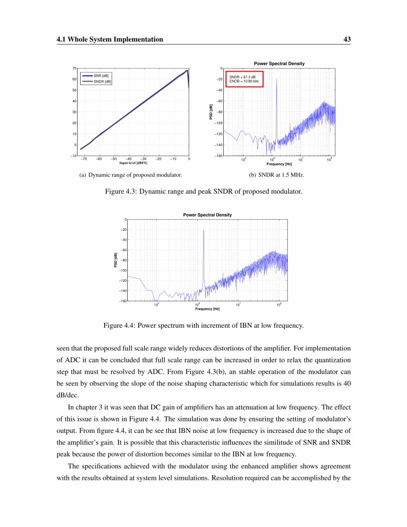
4.1 Whole System Implementation 43
−70 −60 −50 −40 −30 −20 −10 0−10
0
10
20
30
40
50
60
70
Input level [dBFS]
SNR [dB]
SNDR [dB]
(a) Dynamic range of proposed modulator.
105
106
107
108
−160
−140
−120
−100
−80
−60
−40
−20
0
SNDR = 67.3 dB
ENOB = 10.89 bits
Power Spectral Density
Frequency [Hz]
PS
D [
dB
]
(b) SNDR at 1.5 MHz.
Figure 4.3: Dynamic range and peak SNDR of proposed modulator.
105
106
107
108
−160
−140
−120
−100
−80
−60
−40
−20
0
Power Spectral Density
Frequency [Hz]
PS
D [
dB
]
Figure 4.4: Power spectrum with increment of IBN at low frequency.
seen that the proposed full scale range widely reduces distortions of the amplifier. For implementation
of ADC it can be concluded that full scale range can be increased in order to relax the quantization
step that must be resolved by ADC. From Figure 4.3(b), an stable operation of the modulator can
be seen by observing the slope of the noise shaping characteristic which for simulations results is 40
dB/dec.
In chapter 3 it was seen that DC gain of amplifiers has an attenuation at low frequency. The effect
of this issue is shown in Figure 4.4. The simulation was done by ensuring the setting of modulator’s
output. From figure 4.4, it can be see that IBN noise at low frequency is increased due to the shape of
the amplifier’s gain. It is possible that this characteristic influences the similitude of SNR and SNDR
peak because the power of distortion becomes similar to the IBN at low frequency.
The specifications achieved with the modulator using the enhanced amplifier shows agreement
with the results obtained at system level simulations. Resolution required can be accomplished by the
44 Results
Temperature TT FF SS FS SF[C] SNR SNDR SNR SNDR SNR SNDR SNR SNDR SNR SNDR100 65.5 65.3 66.3 66.1 65.8 65.5 66.6 66.3 67.5 66.960 66.1 65.8 65.7 65.5 65.9 65.7 66.9 66.7 66.2 65.9-20 67.6 67.3 67.2 67.1 67.3 67.1 67.2 67.1 67.1 66.8
Table 4.1: Performance summary. SNR and SNDR are expressed in dB.
system proposed while the amplifier has a total power consumption of 6 mW. Below, it will be shown
the influence of PVT variations on the system.
4.1.3 PVT analysis
Robustness of amplifiers was analyzed in chapter 3 where for all corners of process, temperature and
voltage variations the DC gain was maintained around 50 dB. Now, to evaluate the performance of
amplifiers in the modulator, PVT variations are studied in the whole system. Simulation setup is the
same that above simulations but the input level is set to -3 dBFS.
Table 4.1 show the SNR and SNDR achieved for all process and temperature corners. It can
be see that the specification of 62 dB or 10 bits can be accomplished with the system. Minimum
resulting SNR and SNDR is 65.5 dB and 65.3 dB respectively. From simulations performed, it was
seen that for FF process corner the settling time of modulator was increased in comparison with other
process corners. Therefore, simulation results obtained for FF process corner can not be accurate. It is
necessary to review the settling time of the modulator and to do more simulations in order to improve
the accuracy. However, it is expected that maximum achievable resolution does not have significant
changes.
The effects of voltage supply variations on the modulator performance can be seen in Figure
4.5. These simulations was performed by fixing FS process corner and a temperature to 100. The
temperature was chosen by observing that 100 increases the distortion more significantly that others.
From Figure 4.5, it can be seen that modifications in SNR for the variation range is not so wide.
However, its effect in SNDR is clearly shown. As the voltage supply is reduced distortion becomes
more prominent. This result was expected due to the non-linearity dependence of circuits with voltage
supply. As a conclusion, the voltage supply can be reduced to around 1.1 V without strong loss in the
resolution.

4.2 Comparison of Topologies Used 45
1 1.05 1.1 1.15 1.2 1.25 1.3 1.35 1.459
60
61
62
63
64
65
66
67
Power Supply [V]
SNR [dB]
SNDR [dB]
Figure 4.5: Effect of variations on voltage supply.
105
106
107
108
−160
−140
−120
−100
−80
−60
−40
−20
0
SNDR = 53.3 dB
ENOB = 8.57 bits
Power Spectral Density
Frequency [Hz]
PS
D [
dB
]
SNDR = 62.7 dB
ENOB = 10.13 bits
(a) Typical case (gray) and worst case (blue).
105
106
107
108
−160
−140
−120
−100
−80
−60
−40
−20
0
SNDR = 65.9 dB
ENOB = 10.65 bits
Power Spectral Density
Frequency [Hz]
PS
D [
dB
]
SNDR = 64.7 dB
ENOB = 10.46 bits
(b) Typical case (gray) and worst case (blue).
Figure 4.6: Output Power spectrum of the modulator: with miller amplifier (a) and with enhancedOTA (b).
4.2 Comparison of Topologies Used
Figures 4.6(b) and 4.6(a) show typical and worst case power spectrum. It can be observed that the
variation in OpAmp’s DC gain widely modifies the IBN and therefore degrades the SNR. Worst case
refers to minimum DC gain and GBW of amplifiers which were presented in Figure 3.12. Simulations
performed show that the modulator using the enhanced OTA has a minimum SNDR of 64.7 dB while
for Miller amplifier it is 53.3 dB which is significant lower than the required specifications. Clearly,
the enhanced OTA has better performance in comparison with Miller amplifier because it improves
over 10 dB the modulator’s SNDR. Also, from Figure 4.6(b) it can be seen that noise shaping has not
significant variations despite having variations in DC gain. On the other hand, in Figure 4.6(a) a wide
variation in noise shaping is observed .

46 Results
Chapter 5
Conclusions
In this work two OTA are proposed. First amplifier achieves a DC gain of 50 dB but it is still sensitive
to PVT variations and has problems with its common mode voltage. On the other hand, the second
proposal achieves a DC gain over 50 dB while reduces PVT variations maintaining the required spec-
ifications. The problem of reduced gain was overcome by using self-cascode transistors which also
reduced the gain dependence with voltage supply while the process variation was reduced implement-
ing sums of the transconductance. As a result, a robust to PVT OTA with relatively high DC gain is
obtained.
Comparison between Miller amplifier and the proposed amplifier by implementing the whole mod-
ulator show that an improvement over 9 dB in SNDR is achieved with the proposed amplifier. In
simulation results is clearly observed that IBN increases as the amplifier gain decreases which de-
grades the modulator performance.
Using feedback amplifiers, different buffers was proposed. First proposal show a fully differential
buffer that has wide input and output voltage excursion but has output impedance of 2 kΩ. To reduce
this values, single ended buffers was accomplished where the open loop was improved. Final proposal
has wide input and output voltage excursion with output impedance of 55 Ω and reduced PVT varia-
tions. Again, self-cascode transistor was used to improve DC gain.
The study of the technology used is very important to accomplish a successful design. SOI techno-
logy has advantage over Bulk-CMOS technology related to body capacitances and SCE reduction.
However, floating body effects imposes strong issues like the history effects and threshold voltage
variability.
Circuit’s non-idealities are issues that must be taken into account to perform design of a CT Σ∆
modulator. Modeling of these non-idealities is pretty important in order to estimate if a given system
accomplishes the required specifications. As a consequence, a successful circuit implementation de-
pends widely on correct modeling and simulations at system level.

48 Conclusions
The influence of OpAmp’s DC gain over the whole CT Σ∆ modulator is clearly shown in this work.
Minimum gain specification is necessary to ensure the required performance of modulator. Therefore,
the study of the effects of PVT variations on amplifiers is helpful to identify the maximum resolution
achieved by a modulator.
5.1 Future works
Mismatch analysis must be performed to the proposed circuits in order to study its robustness to
statistical variations on its parameter characteristics.
Besides doing mismatch analysis, it is necessary to do the layout to obtain simulations considering
parasitic elements to validate the design.
Despite having a less significant effect on the modulator, ADC is other important building block which
must be reviewed with the purpose of achieving a more efficient modulator implementation.
DACs are other circuits that impose several limitations in CT Σ∆ modulator. Therefore, it is necessary
to analyze DAC implementations and their PVT variations in order to have a robust implementation
of a modulator.
Amplifiers must be designed to improve linearity at voltages below the proposed nominal voltage in
this work.

Bibliography
[1] L. Breems and J. Huijsing, Continuous-Time Sigma-Delta Modulation for A/D Conversion in
Radio Receivers. Kluwer Academic Publishers, 2001.
[2] S. Gambini and J. Rabaey, “A 100KS/s 65dB DR Σ∆ ADC with 0.65V supply voltage,” in Solid
State Circuits Conference, 2007. ESSCIRC 2007. 33rd European, sept. 2007, pp. 202 –205.
[3] M. Ortmanns and F. Gerfers, Continuous-Time Sigma-Delta A/D Conversion. Springer, 2009.
[4] A. Chandrakasan, W. Bowhill, and F. Fox, Design of High-Performance up Circuits. Wiley,
2000.
[5] J. Cherry and W. Snelgrove, Continuous-Time Sigma-Delta Modulators for High-Speed A/D
Conversion. Kluwer Academic Publishers, 2002.
[6] C.-Y. Lu, “Calibrated Continuous-Time Sigma-Delta Modulators,” Ph.D. dissertation, Texas
A&M University, 2010.
[7] A. Marshall and S. Natarajan., SOI Design Analog, Memory and Digital Techniques. Kluwer,
2002.
[8] A. M. Takayasu Sakurai and T. Douseki., Fully-Depleted SOI CMOS Circuits and Technology
for Ultralow-Power Applications. Springer, 2006.
[9] K. Bernstein and N. Rohrer, SOI Circuit Design Concepts. Springer, 2007.
[10] R. Schoofs, M. Steyaert, and W. Sansen, “A 1 GHz continuous-time sigma-delta A/D converter
in 90 nm standard CMOS,” in Microwave Symposium Digest, 2005 IEEE MTT-S International,
june 2005, p. 4 pp.
[11] G. Mitteregger, C. Ebner, S. Mechnig, T. Blon, C. Holuigue, and E. Romani, “A 20-mW 640-
MHz CMOS Continuous-Time ADC With 20-MHz Signal Bandwidth, 80-dB Dynamic Range
and 12-bit ENOB,” Solid-State Circuits, IEEE Journal of, vol. 41, no. 12, pp. 2641 –2649, dec.
2006.
50 BIBLIOGRAPHY
[12] K. Matsukawa, Y. Mitani, M. Takayama, K. Obata, S. Dosho, and A. Matsuzawa, “A Fifth-Order
Continuous-Time Delta-Sigma Modulator With Single-Opamp Resonator,” Solid-State Circuits,
IEEE Journal of, vol. 45, no. 4, pp. 697 –706, april 2010.
[13] K.-C. Hong and H. Chiueh, “A 36-mW 320-MHz CMOS continuous-time sigma-delta modulator
with 10-MHz bandwidth and 12-bit resolution,” in Circuits and Systems (MWSCAS), 2010 53rd
IEEE International Midwest Symposium on, aug. 2010, pp. 725 –728.
[14] S. Paton, A. Di Giandomenico, L. Hernandez, A. Wiesbauer, T. Potscher, and M. Clara, “A
70-mW 300-MHz CMOS continuous-time Σ∆ ADC with 15-MHz bandwidth and 11 bits of
resolution,” Solid-State Circuits, IEEE Journal of, vol. 39, no. 7, pp. 1056 – 1063, july 2004.
[15] L. Dorrer, F. Kuttner, A. Santner, C. Kropf, T. Puaschitz, T. Hartig, and M. Punzenberger, “A
Continuous Σ∆ ADC for Voice Coding with 92dB DR in 45nm CMOS,” in Solid-State Circuits
Conference, 2008. ISSCC 2008. Digest of Technical Papers. IEEE International, feb. 2008, pp.
502 –631.
[16] W. Yang, W. Schofield, H. Shibata, S. Korrapati, A. Shaikh, N. Abaskharoun, and D. Ribner, “A
100mW 10MHz-BW CT Σ∆ Modulator with 87dB DR and 91dBc IMD,” in Solid-State Circuits
Conference, 2008. ISSCC 2008. Digest of Technical Papers. IEEE International, feb. 2008, pp.
498 –631.
[17] Y.-S. Shu, B.-S. Song, and K. Bacrania, “A 65nm CMOS CT Σ∆ Modulator with 81dB DR and
8MHz BW Auto-Tuned by Pulse Injection,” in Solid-State Circuits Conference, 2008. ISSCC
2008. Digest of Technical Papers. IEEE International, feb. 2008, pp. 500 –631.
[18] Y.-C. Lin, W.-H. Hsieh, and C.-C. Hung, “A continuous-time delta-sigma modulator using feed-
back resistors,” in VLSI Design, Automation and Test, 2009. VLSI-DAT ’09. International Sym-
posium on, april 2009, pp. 243 –246.
[19] M. Straayer and M. Perrott, “A 12-Bit, 10-MHz Bandwidth, Continuous-Time Σ∆ ADC With
a 5-Bit, 950-MS/s VCO-Based Quantizer,” Solid-State Circuits, IEEE Journal of, vol. 43, no. 4,
pp. 805 –814, april 2008.
[20] C.-Y. Lu, M. Onabajo, V. Gadde, Y.-C. Lo, H.-P. Chen, V. Periasamy, and J. Silva-Martinez, “A
25 MHz Bandwidth 5th-Order Continuous-Time Low-Pass Sigma-Delta Modulator With 67.7
dB SNDR Using Time-Domain Quantization and Feedback,” Solid-State Circuits, IEEE Journal
of, vol. 45, no. 9, pp. 1795 –1808, sept. 2010.

BIBLIOGRAPHY 51
[21] Y. Chen and K. pang Pun, “A 0.5V 2-1 cascaded continuous-time Delta-Sigma modulator syn-
thesized with a new method,” in Circuits and Systems (MWSCAS), 2010 53rd IEEE International
Midwest Symposium on, aug. 2010, pp. 1165 –1168.
[22] F. Gerfers, M. Ortmanns, and Y. Manoli, “A 1.5-V 12-bit power-efficient continuous-time third-
order Sigma; Delta; modulator,” Solid-State Circuits, IEEE Journal of, vol. 38, no. 8, pp. 1343 –
1352, aug. 2003.
[23] M. Ortmanns, F. Gerfers, and Y. Manoli, “Compensation of finite gain-bandwidth induced er-
rors in continuous-time sigma-delta modulators,” Circuits and Systems I: Regular Papers, IEEE
Transactions on, vol. 51, no. 6, pp. 1088 – 1099, june 2004.
[24] S. Brigati, F. Francesconi, P. Malcovati, D. Tonietto, A. Baschirotto, and F. Maloberti, “Modeling
sigma-delta modulator non-idealities in SIMULINK(R),” in Circuits and Systems, 1999. ISCAS
’99. Proceedings of the 1999 IEEE International Symposium on, vol. 2, jul 1999, pp. 384 –387
vol.2.
[25] R. Lyons, Understandig Digital Signal Processing. Prentice Hall, 2004.
[26] O. Belotti and F. Maloberti, “Design of Continuous-Time Σ∆ modulators with real analog
blocks,” in Ph.D. Research in Microelectronics and Electronics (PRIME), 2010 Conference on,
july 2010, pp. 1 –4.
[27] D. Johns and K. Martin, Analog Integrated Circuit Design. John Wiley & Sons, Inc, 1997.
[28] M. S. L. Yao and W. Sansen, Low power, Low voltage Sigma Delta Modulators in Nanometer
CMOS. Springer, 2006.
[29] R. J. Baker, CMOS Circuit Design, Layout and Simulation. IEEE Press, 2005.
[30] J. Zhang, L. Yao, and Y. Lian, “A 1.2-V 2.7-mW 160MHz continuous-time delta-sigma modu-
lator with input-feedforward structure,” in Custom Integrated Circuits Conference, 2009. CICC
’09. IEEE, sept. 2009, pp. 475 –478.
[31] I. Padilla, “QUIESCENT CURRENT CONTROL CIRCUIT FOR CLASS AB AMPLIFIERS,”
Ph.D. dissertation, New Mexico State University, 2007.