room-temperature application of vo2 microstructures on
TRANSCRIPT

This journal is©The Royal Society of Chemistry 2020 Mater. Adv., 2020, 1, 1685--1694 | 1685
Cite this:Mater. Adv., 2020,
1, 1685
Room-temperature application of VO2
microstructures on rigid and flexible substratesbased on synthesis of crystalline VO2 solution†
Mohammad Taha, *ab Edwin L. H. Mayes,c Matthew R. Field,c Miao Sun,a
Mandeep Singhd and Wenyue Zoud
The insulator-to-metal transition (IMT) in vanadium dioxide (VO2) offers temperature-dependent infrared
wavelength attenuation, rendering it a great contender for bolometers, optoelectronics, memory devices,
smart-windows adaptive thermal camouflage applications. However, the required high temperature
processing (up to 600 1C) of VO2 inhibits its widespread utilization, particularly in applications with low
fabrication temperature limits – such as devices on flexible polymer substrates. This study provides a new
method that relies on van der Waals substrates with inert basal planes and hydrophilic surfaces to overcome
the hurdle of high processing temperatures. Using this method, highly-oriented, optically active crystalline
VO2 was deposited on both glass and flexible polyethylene terephthalate (PET) substrates. We observe VO2
crystals during IMT using transmission electron microscopy (TEM), X-ray photoelectron spectroscopy (XPS)
and report 460% change in transmission on both glass and flexible PET, as well as demonstrating IR
modulation.
Introduction
With ever-increasing global energy demands and continuouslyworsening climate conditions, it is paramount to develop moresophisticated energy solutions, and to not only rely on renew-able energy but to also mitigate excessive energy losses andminimize redundancy. Windows are considered to be a sig-nificant source of energy loss in buildings and other structures.Heating and cooling of buildings accounts for B14% of thetotal energy use in the US.1 Therefore, reducing unnecessaryenergy loss from buildings is a vital part of the roadmaptowards a sustainable future economy. Minimizing energy lossthrough windows may be achieved through thermally respon-sive glazing and coatings, which are an emerging and vital partsof glass technology.2 Dynamic windows, or smart-windows,change their optical properties by utilizing materials that feature
photochromism, electrochromism or thermochromism to over-come the traditionally wasteful nature of windows.3
Monoclinic vanadium dioxide (VO2) is both electrochromicand thermochromic, and is thus suitable to be applied in smartdynamic coatings,4–6 since it simultaneously blocks ultraviolet(UV) radiation and modulates infrared (IR) light.7–11 CrystallineVO2 experiences thermochromism at B68 1C, when the mate-rial switches from a semiconducting monoclinic to a conduc-tive tetragonal configuration. As the material changes crystalconfiguration, it experiences an increase in free charge carriers,leading to a metallic state. Metallic VO2 exhibits a dramaticallyreduced transmission in the IR, microwave and terahertzwavelengths range when compared to the semiconductingphase.12–18 The insulator-to-metal transition (IMT) of vanadiumoxides depends on the microstructure, morphology and stoichio-metry of the oxide. The transition generally occurs within pico/femtoseconds,19 making vanadium oxide a promising candidatefor electronic switch components in integrated circuits,20 smartwindow coatings,21–23 tunable antennas24,25 and metamaterials.26
However, the development of commercially viable synthesismethods for VO2 is hindered, due to inherent difficulties asso-ciated with the existence of vanadium oxides of different stoichio-metry and pronounced polymorphism. With 15–20 other stablevanadium oxide phases, the formation of VO2 occurs only overspecific ranges of oxygen partial pressures and temperatures.27,28
Therefore, vapor phase VO2 synthesis methods such assputtering29–34 and chemical-vapor deposition (CVD)35–38
a Department of Electrical and Electronic Engineering, School of Engineering,
The University of Melbourne, Parkville, VIC, 3010, Australia.
E-mail: [email protected] RMIT University, Melbourne, VIC, 3000, Australiac RMIT Microscopy & Microanalysis Facility, College of Science, Engineering and
Health, RMIT University, Melbourne, VIC, 3000, Australiad Ian Potter NanoBioSensing Facility, NanoBiotechnology Research Laboratory,
School of Science, RMIT University, Melbourne, VIC, 3000, Australia
† Electronic supplementary information (ESI) available. See DOI: 10.1039/d0ma00338g
Received 22nd May 2020,Accepted 23rd August 2020
DOI: 10.1039/d0ma00338g
rsc.li/materials-advances
MaterialsAdvances
PAPER
Ope
n A
cces
s A
rtic
le. P
ublis
hed
on 0
9 Se
ptem
ber
2020
. Dow
nloa
ded
on 1
2/7/
2021
1:1
8:43
AM
. T
his
artic
le is
lice
nsed
und
er a
Cre
ativ
e C
omm
ons
Attr
ibut
ion
3.0
Unp
orte
d L
icen
ce.
View Article OnlineView Journal | View Issue

1686 | Mater. Adv., 2020, 1, 1685--1694 This journal is©The Royal Society of Chemistry 2020
are widely employed, since they offer a high degree of controlover the partial oxygen pressure and can be operated at hightemperatures.
Solution-based methods such as sol–gel10,39,40 and polymerassisted deposition (PAD)40,41 have also been reported. Thesemethods utilize chemical precursors dissolved in a liquidmedium. Such synthesis techniques result in colloidal suspen-sions, which are excellent for coating large areas using solutionprocessing; however, they still pose limitations on the applica-tion of VO2 solution to temperature-sensitive surfaces andfabrics, since solutions do not undergo IMT without a subse-quent annealing step. As a result, they are not suitable forapplication in a large number of thermally unstable existingwindow technologies (i.e. acrylic windows) or the retrofitting ofexisting windows or integration with flexible substrates withlow melting points, or fabrics. Importantly, even though hydro-thermal processes are widely used in VO2 synthesis, they do notbenefit from the level of morphological and crystallographiccontrol available when using physical or chemical vapor deposi-tion techniques.
Herein, we report a two-step fabrication method that allowsthe synthesis of fully-functional VO2 using physical vapordeposition (PVD) techniques. The VO2 can then be suspendedto create a functional colloidal ink that can be applied to anysurface, without the need for further post-application anneal-ing. We use highly hydrophilic mica growth substrates todevelop this technology, enabling the highly-oriented growthof crystalline VO2 films through pulsed-DC magnetronsputtering,42–44 while allowing the lift-off into solution post-synthesis. We characterize the VO2 suspension and observeIMT using in situ transmission electron microscopy (TEM),selected area electron diffraction (SAED) and X-ray photoelec-tron spectroscopy (XPS), before introducing VO2 to standardglass and a flexible substrate with low thermal stability (PET)for optical characterization.
Experimental sectionVO2 solution synthesis
The VO2 thin films are deposited onto mica using pulsed DCmagnetron sputtering technique. A vanadium target (99.98%purity) was set up at B120 mm from the substrates with basepressure of B4� 10�7 and working pressure of B3� 10�3. TheAr : O2 flow rate of the gas mixture in the sputtering chamberwas 13.25 : 6.25 sccm. Sputtering was conducted at 200 W withpulse frequency and reverse time at 25 kHz and 5 ms respectively.VO2 films were then annealed in a furnace, and evacuated to lowvacuum to achieve a pressure of B50–150 mTorr, at 550 1C for90 min. Mica coated with crystalline VO2 was immersed in waterto allow for delamination (sonication was not essential, but itexpediates the delamination of VO2 crystals). The resultantsolution was placed in an oven to undergo slow evaporationovernight at 90 1C, before being allowed to cool down to roomtemperature. IPA was added to the crystals, forming a VO2
solution that can be evaporated at room temperature.
X-ray photoelectron spectroscopy (XPS) and X-ray diffraction(XRD)
XPS analysis was conducted using a Thermo Scientific K-Alphainstrument under ultrahigh vacuum (base pressure o 1 �10�7 Pa). An aluminum Ka X-ray radiation source with energyof 1486.6 eV was used. All core-level spectra of the elementswere collected at pass energy of 50 eV and analyzed withAdvantage software. The binding energies of all principalelements were referenced to the adventitious carbon (C 1s) ofbinding energy 284.6 eV. XRD diffractograms are producedusing X-ray diffraction powder analyser (D2 Phaser, Bruker).
UV-Vis and bandgap measurements
The UV-Vis absorbance measurements of the aqueous suspen-sion of VO2 were carried out using an Agilent Cary 7000 UV-Vis-NIR spectrophotometer equipped with an integrating sphere.
Raman spectroscopy
Raman spectra were acquired on a Horiba LabRAM HR Evolu-tion Raman spectrometer using a 532 nm laser with 0.5 mWpower and Magnification during the experiment was set to�100. In this experiment, pure Si was used as substrates.
Scanning electron microscopy (SEM)
The FEI Verios 460L was used to collect scanning electronmicrographs. Samples were coated with 5 nm of Pt beforebeing placed in the chamber to prevent surface discharge.FEI Helios Nanolab 600 Dual Beam FIB-SEM was used to collectmicrographs of cross sections of VO2 microstructures on glass.
In situ transmission electron microscopy (TEM) and electronenergy-loss spectroscopy (EELS)
TEM and EELS measurements were collected by drop-castingVO2 crystals onto a Protochips heating chip and mounting it ina Fusion heating/biasing sample holder. TEM in situ analysisfor diffraction and imaging were then performed on a JEOL2100F TEM operating at 200 kV. The following parameters wereused (Spot size = 1, alpha = 3, condenser aperture number 3(CA3), selected area aperture number 2 (SA2)) and the flake wasfully covered during the experiment. EELS analysis was per-formed using the same sample and holder combination in aJEOL F200 TEM operating at 200 kV in STEM mode. A GatanContinuum S spectrometer was used to collect core loss V L2,3
edge spectra.Data was collected at initially conditions (B22 1C) and again
at elevated temperature (120 1C) to ensure the transition fromthe M1 monoclinic phase to the tetragonal phase had com-pleted. As the transition is fully reversible, several temperaturesweeps were collected for each data type and for video of thetransition process.
In situ X-ray photoelectron spectroscopy (XPS)
XPS with in situ heating was performed using a Kratos AxisSupra with monochromated Al Ka X-ray source (1486.6 eV)
Paper Materials Advances
Ope
n A
cces
s A
rtic
le. P
ublis
hed
on 0
9 Se
ptem
ber
2020
. Dow
nloa
ded
on 1
2/7/
2021
1:1
8:43
AM
. T
his
artic
le is
lice
nsed
und
er a
Cre
ativ
e C
omm
ons
Attr
ibut
ion
3.0
Unp
orte
d L
icen
ce.
View Article Online
This journal is©The Royal Society of Chemistry 2020 Mater. Adv., 2020, 1, 1685--1694 | 1687
operated at 30 mA emission. The samples were pre-cleanedusing 5 s of 2 keV Ar1000 gas cluster ion sputtering.
Optical measurements
UV-Vis-IR transmission spectra were collected using a CRAIC20/30 microspectrophotometer. A custom-made stage was usedto conduct in situ measuring transmission through the sam-ples. Optical transmission values were collected and recordedat different temperature to observe thermochromic behaviourof the microstructures.
Infrared imaging
Temperature was measured by placing the samples and thecontrol on a hot plate and taking infrared images using theFLIR C2 education kit.
VO2 optical transmission simulation
VO2 crystal drop-cast on a quartz substrate was carried outusing the finite element method implemented in COMSOLMultiphysics. The simulation model consists of 1 mm thicklayer of a semi-infinite glass substrate with the refractive indexvalue, 1.5. The refractive indices of quartz for different wave-lengths were taken from COMSOL embedded material library. AVO2 crystal layer with different size of flakes was added on thetop of the quartz substrate. The thickness of VO2 was setto 80 nm due to the average measurement under FIB to studyits effect on transmission and switching on the semiconductorphase and metallic phase. A 1.5 mm air superstrate was con-structed on the top of VO2 section. To simulate a large areaof VO2 drop, periodic boundary condition was applied on foursides of the model. The incident light was set to propagate
along the perpendicular to the substrate surface with TEpolarization using port boundary condition. A 300 nm Perfectmatch layer (PML) was added to the top boundary and thebottom boundary to absorb the outgoing wave and to ensurethat no reflection was present in the interior region.
Results and discussionSynthesis of crystalline VO2 solution
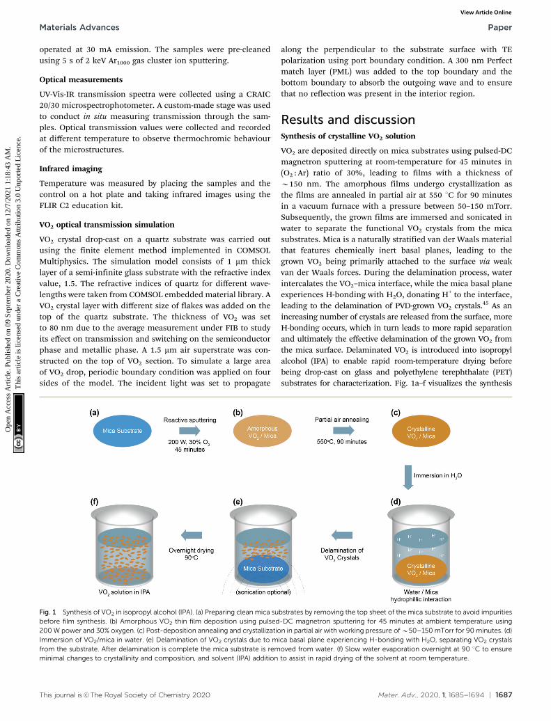
VO2 are deposited directly on mica substrates using pulsed-DCmagnetron sputtering at room-temperature for 45 minutes in(O2 : Ar) ratio of 30%, leading to films with a thickness ofB150 nm. The amorphous films undergo crystallization asthe films are annealed in partial air at 550 1C for 90 minutesin a vacuum furnace with a pressure between 50–150 mTorr.Subsequently, the grown films are immersed and sonicated inwater to separate the functional VO2 crystals from the micasubstrates. Mica is a naturally stratified van der Waals materialthat features chemically inert basal planes, leading to thegrown VO2 being primarily attached to the surface via weakvan der Waals forces. During the delamination process, waterintercalates the VO2–mica interface, while the mica basal planeexperiences H-bonding with H2O, donating H+ to the interface,leading to the delamination of PVD-grown VO2 crystals.45 As anincreasing number of crystals are released from the surface, moreH-bonding occurs, which in turn leads to more rapid separationand ultimately the effective delamination of the grown VO2 fromthe mica surface. Delaminated VO2 is introduced into isopropylalcohol (IPA) to enable rapid room-temperature drying beforebeing drop-cast on glass and polyethylene terephthalate (PET)substrates for characterization. Fig. 1a–f visualizes the synthesis
Fig. 1 Synthesis of VO2 in isopropyl alcohol (IPA). (a) Preparing clean mica substrates by removing the top sheet of the mica substrate to avoid impuritiesbefore film synthesis. (b) Amorphous VO2 thin film deposition using pulsed-DC magnetron sputtering for 45 minutes at ambient temperature using200 W power and 30% oxygen. (c) Post-deposition annealing and crystallization in partial air with working pressure of B50–150 mTorr for 90 minutes. (d)Immersion of VO2/mica in water. (e) Delamination of VO2 crystals due to mica basal plane experiencing H-bonding with H2O, separating VO2 crystalsfrom the substrate. After delamination is complete the mica substrate is removed from water. (f) Slow water evaporation overnight at 90 1C to ensureminimal changes to crystallinity and composition, and solvent (IPA) addition to assist in rapid drying of the solvent at room temperature.
Materials Advances Paper
Ope
n A
cces
s A
rtic
le. P
ublis
hed
on 0
9 Se
ptem
ber
2020
. Dow
nloa
ded
on 1
2/7/
2021
1:1
8:43
AM
. T
his
artic
le is
lice
nsed
und
er a
Cre
ativ
e C
omm
ons
Attr
ibut
ion
3.0
Unp
orte
d L
icen
ce.
View Article Online

1688 | Mater. Adv., 2020, 1, 1685--1694 This journal is©The Royal Society of Chemistry 2020
process leading to highly oriented crystalline VO2, and the mecha-nism of separation from the mica substrate. An image of the VO2
suspension is shown in the ESI,† in Fig. S1.
Composition, optical bandgap, Raman spectra and surfacemorphology of VO2 crystals
The two-step process reported here includes suspending VO2
microstructures first in water, then in isopropyl alcohol (IPA).Consequently, it is of great importance to verify that thesynthesized VO2 crystals maintain their stoichiometry andfunctionality, and do not undergo chemical reactions whilebeing suspended. X-ray photoelectron spectroscopy (XPS) wasused to detect any possible changes to the stoichiometry andbonding of the oxygen and vanadium atoms. Fig. S2 (ESI†)shows the XPS survey scan of the VO2 microstructures synthe-sised for elemental analysis. The presence V 2p, O 1s peaks andhigh energy core level peaks OKLL confirms the presence of allthe composing elements. Fig. 2a and b show the vanadium andoxygen core-level XPS before and after the separation fromthe mica substrate. The samples exhibit a V 2p3/2 peak atB516.4 eV, which is associated with vanadium in the V4+
oxidation state.46–53 The O 1s peaks at B530 eV correspondsto V–O bonding, as indicated in the literature,46,50,54 while532 eV corresponds to oxygen atoms in the Si–O in the substrate.55
These findings confirm that the grown crystals as well as thedelaminated samples that have been drop-cast on glass sub-strates for analysis are indeed VO2. Overall, aside from the Si–Opeak in the drop-cast VO2, binding energies and oxidation statescorrelate well, indicating that the composition of VO2 crystalswithstands the delamination process.
The optical properties of the synthesized VO2 solution wereinvestigated utilizing solution-based UV-Vis spectroscopy.Fig. 3a inset shows the optical absorption spectrum of drop-cast VO2. Tauc plot analysis was performed to determine theoptical bandgap of the synthesized material. Considering com-position, oxidation state of vanadium and bulk crystallinity ofVO2 in Fig. 3 a Tauc plot is a beneficial correlation in bandgapbetween VO2 synthesized here and reported pristine VO2 struc-tures. The spectrum indicates that the crystals in solution areVO2, since the determined bandgap between V 3d8 and 3p* ofB0.72 eV is characteristic for pristine VO2,56–62 while other
possible vanadium oxides such as V2O5 feature wider gaps ofB2.35 eV.62,63 These measurements confirm that there are noother vanadium oxides present since the bandgap measures ischaracteristic to VO2. In Fig. 3a, a B1.95 eV bandgap is presentbetween O 2pp and V 3d8, similar to literature reports.62 Thisbandgap is born to the admixture of vanadium and oxygenbands in VO2, however, this second bandgap is only slightlyaffected by IMT in VO2, since it remains intact while the V 3d8
and 3p* bandgap collapses. The Raman spectrum of thesynthesized VO2 crystals is shown in Fig. 3b. The observedvibrational modes at 285 and 407 cm�1 are associated with theV–O bending mode. The peak at B143 cm�1 corresponds to theBg symmetry,64–66 while the peak at B97 cm�1 is indicative of atwo dimensional (2D) layered architecture, since this modearises from the translated neighboring layers.67–75 The peakat B520 cm�1 can be attributed to the silicon substrate thatwas used during the measurement.76 Other phonon modes at195 (Ag), 225 (Ag), 304 (Ag), 439 (Bg), 615 (Ag) and 700 cm�1
wavenumbers are reported VO2 phonon vibrations.70–75
Fig. S3a and b (ESI†) show the X-ray diffraction (XRD)diffractograms for the microstructures before and after thedelamination process. Fig. S3a (ESI†) is dominated by the peaksof the mica crystal77 and due to the potential overlap with thediffraction features of the substrate mica crystals and VO2
78–80
XRD could not be used to unambiguously analyse the crystalmicrostructure of the VO2 crystals structure. Without furthersteps to remove all mica, some is unavoidably transferred intosolution alongside the VO2; however, it is unlikely to affect theoptical properties of the solution processed VO2 due to the widebandgap and the absence of IMT in mica. Henceforth, in depthanalysis to in situ transmission electron microscopy (TEM),selected area electron diffraction (SAED), electron energy loss
Fig. 2 XPS spectra of vanadium (V 2p3/2) and oxygen (O 1s) for (a) VO2
films on mica and (b) drop-cast VO2 on glass, showing peaks at B530 and532 eV (which indicate the V–O bonding and Si–O peak), and a peak atB516.4 eV (associated with vanadium in the V4+ oxidation).
Fig. 3 (a) A plot of (ahn)2 versus photon energy for VO2 solution. Red lineshows extrapolation to the (ahn)2 = 0, indicating the optical energy gapEOpt
g and optical absorbance. The blue line shows a second bandgap,which is born to the admixture of vanadium and oxygen bands in VO2.(b) Raman spectra for VO2 crystals on glass with an optical microscope image ofa VO2 crystal. SEM image (15 000� magnification) are shown for (c) VO2
film on mica, and (d) VO2 crystals on glass, highlighting the difference inmorphology and crystal structure between VO2 thin film on mica beforedelamination and VO2 microstructures after the delamination process.
Paper Materials Advances
Ope
n A
cces
s A
rtic
le. P
ublis
hed
on 0
9 Se
ptem
ber
2020
. Dow
nloa
ded
on 1
2/7/
2021
1:1
8:43
AM
. T
his
artic
le is
lice
nsed
und
er a
Cre
ativ
e C
omm
ons
Attr
ibut
ion
3.0
Unp
orte
d L
icen
ce.
View Article Online

This journal is©The Royal Society of Chemistry 2020 Mater. Adv., 2020, 1, 1685--1694 | 1689
spectroscopy (EELS) and X-ray photoelectron microscopy (XPS)are relied upon to both examine and verify the monoclinic totetragonal transition characteristic to VO2.
The scanning electron microscopy (SEM) image in Fig. 3cshows the VO2 thin film before the delamination process. Thefilms show some uniformity, while the VO2 microstructuresshown in Fig. 3d are non-uniform and have a different andvarying morphology. As parts of the films break during dela-mination, comparisons in surface roughness using atomicforce microscopy (AFM) are not effective, especially in thecontext of the development of crystalline VO2 solution.Fig. 3d confirms the layered nature of the VO2 crystals, reveal-ing sheet sizes in the range of 0.5 to 10 mm. Particle morphologyis observed to be not uniform, with substantial size and shapevariation, while pinholes are prevalent. Cracking of the VO2
potentially originates during the manual handling of the micasubstrate and diffusion-based delamination process that occurswhen samples are immersed in water. Further SEM images dis-playing similar morphology are shown in the ESI† in Fig. S4a–f. Theobserved overall consistency in morphology between samplesattests to the reproducible nature of the process.
In situ characterization of VO2 crystalsIn situ transmission electron microscopy (TEM), selected areaelectron diffraction (SAED) and electron energy lossspectroscopy (EELS)
The microcrystalline and electronic structure of VO2 crystalsduring the temperature-induced transition were studied usinghigh resolution transmission electron microscopy (HRTEM),selected area electron diffraction (SAED) and electron energyloss spectroscopy (EELS). HRTEM and SAED patterns wereanalyzed and interpreted utilizing Java Electron MicroscopySoftware (JEMS) simulations and SingleCrystal 4 software. Thedata used for analysis is shown in Fig. S5 (ESI†). Fig. 4a–c showHRTEM images of VO2 drop-cast on a heating chip duringdifferent stages of the IMT. The calculated lattice spacing of theVO2 crystal at room temperature (Fig. 4a) is B3.3 Å along theh110i axis, which is consistent with the monoclinic phase ofVO2.81 The VO2 lattice was found to be highly oriented, and theSAED pattern shows a single crystal over the selected area,which attests to the high crystal quality of the synthesized VO2.As the temperature of the sample is increased (Fig. 4a–c), themorphological change of the VO2 crystals can be observed,leading to images (a) before, (c) during, and (b) after IMT. Thedashed red circles in Fig. 4a–c highlight the edge of the crystal,where the change of the crystal phase from monoclinic totetragonal coordination is particularly apparent through rever-sible change in contrast, which can be ascribed to change inphase (see ESI,† S5 Video Image 1).
It is observed that both the surfaces and edges of the crystalIt is observed that both the surfaces and edges of the crystaltransition move through three distinct steps. The monoclinicstate is observed at room temperature. During transition, thecrystal is in a transient state, which is indicated by the dramatic
difference in contrast between Fig. 4c and the structures inFig. 4a and b. The low contrast observed in the transient statecan arise from factors such as thermal fluctuation and bound-ary movement. Furthermore, it can indicate higher electrontransmission through VO2 microstructures. With the contrastbeing the result of a higher degree of scattering caused bymicrostructures in motion in the less stable transient stateduring IMT. It is noteworthy that the crystal transition ispossible to observe, even though it is reported that IMT inVO2 occurs in the order of pico/femtoseconds82 due to micro-structures undergoing phase transition independently.83
The microstructural change in Fig. 4a–c is reversible, andthis can be seen in Video Image 1 of the VO2 crystal transfor-mation in the ESI.† It is also noted that the TEM heating chip isheated to 120 1C, even though VO2 IMT temperature is 68 1C.This ensured the entire heated area of the chip was at above theIMT transition temperature and would remain so for theduration of the required measurements. In the monoclinicstates, diffraction patters at VO2 (�1, �1, 0), (1, 1, 0), (�3, 0, 2),(3, 0, �2), (�2, 1, 2), (2, �1, �2), (�1, 2, 2) and (1, �2, �2) areobserved in addition to high-order Lau zone (HOLZ) reflectioncharacteristic to monoclinic VO2. IMT as observed by electrondiffraction is characterized by the disappearance of the reflec-tion along the h011i axis in the tetragonal state in Fig. 4band the emergence of diffraction patterns at VO2 (�1, 1, �1),(1, �1, 1), (�3, 2, 0), (3, �2, 0), (2, �1, �1), and (�2, 1, 1). Thisobservation results from the rearrangement of VO2 microstruc-tures into linear chains as the microstructures moves betweenthe monoclinic and the tetragonal states. The insets in Fig. 4aand b show selected area electron diffraction (SAED) patternbefore and after the transition. As expected, the patterns corre-spond to the monoclinic and tetragonal phases of VO2.53,84–86 The
Fig. 4 Transmission electron microscopy (TEM), high-resolution transmis-sion electron microscopy (HRTEM) and selected area electron diffraction(SAED) pattern at: (a) room temperature (monoclinic VO2 phase [�2, 2, �3]zone) and (b) 120 1C (tetragonal VO2 phase [2, 3, 1] zone). (c) TEM at 100 1C.(d) Electron energy-loss spectroscopy (EELS) at room temperature (cyan) and120 1C (purple).
Materials Advances Paper
Ope
n A
cces
s A
rtic
le. P
ublis
hed
on 0
9 Se
ptem
ber
2020
. Dow
nloa
ded
on 1
2/7/
2021
1:1
8:43
AM
. T
his
artic
le is
lice
nsed
und
er a
Cre
ativ
e C
omm
ons
Attr
ibut
ion
3.0
Unp
orte
d L
icen
ce.
View Article Online

1690 | Mater. Adv., 2020, 1, 1685--1694 This journal is©The Royal Society of Chemistry 2020
high switching speed of VO2 is more apparent in SAED videoimaging as well as the in situ collection of SAED patterns, whichare provided in the ESI,† S5 Video Image 2. Since microstructuresundergo IMT independently, SAED patterns reflect a single micro-structure during this process, and SAED patterns for the transientstate are not possible to observe. The high switching speed of VO2
is distinguished in Video Image 2 (ESI†) through the unchangedtimestamp (2 : 29 : 214) in the video image before and after IMT,which emphasizes that IMT switching is faster than the resolutionthe clock provides. The electronic structure of the VO2 crystal wasinvestigated through in situ EELS measurements before and afterIMT. Fig. 4d shows a typical VO2 EELS spectrum featuring theV-L3, V-L2 and O-K edge onset at 513, 521, 532 eV respectively, andatomic ratio of vanadium to oxygen of B2.0.87,88 The overall V-L3,V-L2 and O-K edge onset and atomic ratios in the insulating andthe metallic states in Fig. 4d remains unchanged, since IMT inVO2 is a reversible change in electronic, structural and inter/intraband interactions. A subtle change in the electronic structure isobserved, indicated by the broadening of the O-K onset in theinsulating state. IMT impact on band interactions can be recog-nized since the O-K edge measures dipole-allowed core-holeinteractions between the O 1s to unoccupied O 2p and theV 3d8, due to the organization of O 2p in symmetries that allowthe mixture of O 2p and V 3d states.89,90 Fig. 4d highlights thedifferences in the O-K edge between insulating and metallic VO2.In the insulating state, V 3d8* is unoccupied, displaying a lowerelectron energy loss that leads to a higher full width halfmaximum (FWHM) of 2.56. In contrast, V 3d8* is merged withV 3d8 and is occupied in the metallic state of VO2, causing it togenerate a greater electron energy loss and a lower FWHM of 1.72.This change in the O-K edge indicates changes in the V 3d8* bandduring IMT, and is congruent with similar literature reports.91
In situ EELS measurements indicates the changes in the electronicstructure to the V 3d8* band in VO2 during IMT and in situ TEMand SAED observations conclusively verify that VO2 crystalsundergo IMT with changes in morphology. Therefore, we candetermine that VO2 crystals change in both electronic structureand morphology during phase change. However, more accuratein-depth analysis of band transitions and interactions requires theutilization of in situ X-ray photoelectron spectroscopy (XPS).
In situ X-ray photoelectron microscopy (XPS)
In a monoclinic VO2 crystal system, the V 3d8 splits into twoenergy bands, V 3d8 and V 3d8*, and the insulating forbiddenband of B0.7 eV between V 3dp* and V 3d8 is formed. WhenVO2 undergoes IMT, the forbidden band collapses and theV 3d8 band extends into the conduction band, forming themetallic tetragonal VO2 crystal system.60,92
Consequently, valence band XPS can be used to observe theshift in the V 3d band to the Fermi level when the IMT occursand the band gap is collapsed. Fig. 5a shows XPS spectra ofcore-levels at 20 1C (room temperature) and after heating in situto 120 1C. Symmetric broadening of the V 2p peaks by B1.5 eVis observed above the IMT temperature, which is in agreementwith previous reports.47,93 The broadening is explained by theColoumb attractive force between the V 2p core-hole and the
localized electrons in the V 3d band at the Fermi level, whichhas been estimated to be 1.5 eV for VO2.94 The instantaneousinteractions between the core-hole level and the valence bandelectrons lead to this artifact in the V 2p3/2 peak in the core-levelspectrum. Fig. 5b shows the valence band spectra of the VO2
sample at 20 1C and 120 1C. A B0.7 eV prominent shift of theV 3d band towards the Fermi level can be observed (see insetFig. 5b) after the collapse of the forbidden band.
IMT in VO2 microstructures on glass,flexible substrates and thermalattenuation
After verifying IMT behavior using in situ characterizations ofVO2 crystals, the functionality of the synthesized VO2 crystalsfor thermal camouflage and thermal management was exam-ined. The colloidal VO2 is drop-cast on glass to collect in situUV-Vis-IR spectra, in order to ensure that the drop-cast micro-structures are optically active. The temperature dependenttransmittance data in Fig. 6a and b reveal optical switching ofthe drop-cast crystals on the glass surface. In Fig. 6b, narrowhysteresis can be observed, which is an artefact of the hysteresisloop for each VO2 crystal in the drop-cast system. VO2 micro-structures undergo IMT independently, and therefore have anindependent hysteresis loop. The difference in the hysteresisloops in bulk VO2 crystals arises from the presence of a largenumber of crystals of various size in VO2 system.95 Overall, achange in transmission was observed at 2000 nm of over 60%,with complete switching occurring at roughly 70 1C, which isexpected for VO2.
The colloidal VO2 system synthesized here can be depositedonto temperature-sensitive substrates such as PET and sodalime glass, which are otherwise incompatible with VO2 proces-sing, due to their low melting temperatures. Fig. 6c shows a VO2
film on a flexible PET substrate, featuring the characteristicthermochromic behavior of VO2. The PET samples led to aninfrared transmission drop of 460%, which is comparableto the results obtained for glass substrates, shown in Fig. 6a.The successful demonstration on PET substrates coated withfunctional VO2, offering temperature dependent transparency
Fig. 5 (a) X-ray photoelectron spectroscopy (XPS) of core-levels of VO2
microstructures at 20 1C (cyan) and 120 1C (red) showing broadening ofthe V 2p by 1.5 eV. (b) Valence band spectra of VO2 microstructures at20 1C (cyan) and 120 1C (red). The enlarged inset shows shift in the V 3dband by 0.66 eV.
Paper Materials Advances
Ope
n A
cces
s A
rtic
le. P
ublis
hed
on 0
9 Se
ptem
ber
2020
. Dow
nloa
ded
on 1
2/7/
2021
1:1
8:43
AM
. T
his
artic
le is
lice
nsed
und
er a
Cre
ativ
e C
omm
ons
Attr
ibut
ion
3.0
Unp
orte
d L
icen
ce.
View Article Online

This journal is©The Royal Society of Chemistry 2020 Mater. Adv., 2020, 1, 1685--1694 | 1691
switching, serves to validate the versatility of the developedcolloidal VO2. As shown in the inset of Fig. 6c, the VO2/PET
remains the flexible feature of PET preserving the integrity andflexible properties of the PET substrate.
The IMT behavior and optical functionality of drop-cast VO2
microstructures in Fig. 6a and c correlate to the simulationresult obtained in Fig. 6d with simulated 3D crystals (inset).Simulated crystals suggest that VO2 crystals can still undergoIMT, even though they form discontinuous plates. These simu-lated crystals only approximate SEM images and do not exactlyrepresent the morphology of the VO2 microstructures mea-sured, so a degree of mismatch between simulated crystalsand measurements is to be expected. Moreover, variation inthe refractive index between VO2 microstructures synthesizedand values used for simulation leads to different magnitude ofchange between the insulator and the metal states.96 Fig. S2d–fin the ESI† examines a cross section of VO2 crystals drop-caston glass. The cross section shows an overlap of multiplecrystals with different thicknesses. However, this variation doesnot impact the IMT behavior observed or the optical perfor-mance measured for the bulk of the VO2 microstructures onboth glass and PET.
Glass and PET samples were coated with a 50 nm gold layer,in order to conduct IR camera tests to demonstrate the char-acteristic infrared attenuation of VO2 microstructures. Themetal layer is necessary to increase the accuracy of the thermalcamera, since it measures opaque surfaces more accuratelythan transparent materials and microstructures. Fig. 7a–e showboth the optical and infrared images of the VO2 coated glassand PET, and the control as marked. The control consists of
Fig. 6 Functional VO2 solution drop-cast on glass and PET. (a) UV-Vis-IRtransmission spectra of VO2 solution drop-cast on glass. (b) Hysteresiscycle of VO2 crystals on glass measured at the 2000 nm wavelength duringthe heating (red) and cooling (blue) cycles. (c) UV-Vis-IR spectra of VO2
solution on PET and image of the VO2 microstructures realized onthermally unstable PET (inset). (d) Simulated insulator and metal states ofVO2 based on change of refractive index observed in VO2 microstructureson glass. 3D module used based in SEM images collected of the VO2
crystals drop-cast on glass (inset).
Fig. 7 (a) Optical image of the experimental setup to measure total infrared radiation of gold coated glass and PET controls and VO2 on glass and PET (asmarked). Infrared imaging of glass and PET controls at: (b) B30 1C and (c) B100 1C showing apparent temperatures of 30.8 1C and 91.2 1C respectively.Infrared imaging of gold coated VO2 microstructures on glass and PET at: (d) B30 1C and (e) B100 1C demonstrating thermal camouflage by showingapparent temperatures of 19.3 1C and 43.7 1C respectively. The colour contrast of the infrared images demonstrates the hot and cold surface with reference toone another. (f) Total radiation of VO2 microstructures drop-cast on glass and PET showing a total infrared radiation reduction capability of VO2 coated surfacesboth rigid and flexible. Overall, the estimated temperature attenuation is B36% at 30 1C with B0.3%/1C reduction with rising temperatures.
Materials Advances Paper
Ope
n A
cces
s A
rtic
le. P
ublis
hed
on 0
9 Se
ptem
ber
2020
. Dow
nloa
ded
on 1
2/7/
2021
1:1
8:43
AM
. T
his
artic
le is
lice
nsed
und
er a
Cre
ativ
e C
omm
ons
Attr
ibut
ion
3.0
Unp
orte
d L
icen
ce.
View Article Online
1692 | Mater. Adv., 2020, 1, 1685--1694 This journal is©The Royal Society of Chemistry 2020
gold-coated glass and PET, to confirm that the reduction inradiation is representative of VO2 behavior. Fig. 7b and c showthe temperature measured on the surface of the glass and PETcontrol at B30 1C and B100 1C. Fig. 7d and e establish thatthermal camouflage is compatible and transferrable to PET.Infrared imaging indicates total reduction in radiation percep-tion of approximately 10 1C when the set temperature is B30 1Cand exceeding 50 1C at B100 1C. The infrared imaging inFig. 7e and f confirms the efficient attenuation of infraredradiation across the entire surface of both glass and PET, andthe suitability of VO2 for IR radiation attenuation even attemperatures as low as 30 1C. Fig. 7f contrasts both glass andPET substrate coated with VO2 and their application for ther-mal attenuation. Glass substrates show a greater thermalattenuation than its PET counterpart due to the differences inthermal properties and substrate thickness between the twosubstrates. Nevertheless, those differences do not contradictthe general trends of the substrates thermally responsiveproperties at different temperatures recorded in Fig. 7f.
Conclusions
Herein a synthesis method is demonstrated that overcomes thehigh processing temperatures required for producing thermo-chromic VO2 films, and the associated limitations in the choiceof substrates. Using a van der Waals substrate with inert basalplanes and hydrophilic surfaces such as mica allows for the faciledelamination of the synthesized oxide into aqueous colloidalsuspension. The synthesis strategy allows to effectively separatethe high temperature processing steps, enabling the deposition ofhigh quality VO2 onto arbitrary substrates. TEM, EELS and XPSstudies assert the high quality of the transferred VO2 crystals. Theinsulator-to-metal transition can be directly observed in operandoduring temperature-dependent high resolution TEM, leading tothe observation of changes in the microcrystalline and electronicmicrostructures. In situ XPS findings highlighted the impact offorbidden bandgap collapse on both deep core-level spectra andvalence band measurements. The optical properties of the depos-ited films featured excellent optical switching performance andinfrared radiation attenuation. Similar optical performance wasobserved for flexible polyethylene terephthalate (PET) and glasssubstrates, featuring a change in transmission exceeding 60% at2000 nm and adaptive thermal attenuation. This work offers thecapability to readily synthesize VO2 and subsequently deposit itfrom solution at room temperature onto any desired substrates,including substrates that are incompatible with high temperatureprocessing. This extends IMT applications to low-cost, flexible, buttemperature sensitive platforms, expanding the scope of futureVO2-based devices and applications. Furthermore, this methodcan likely be utilized for the synthesis of other materials that canbe grown on mica to introduce colloidal heterostructures.
Conflicts of interest
There are no conflicts to declare.
Acknowledgements
The authors also acknowledge the facilities and technicalassistance of the Micro Nano Research Facility (MNRF), theRMIT Microscopy and Microanalysis Research Facility (RMMF)and the Melbourne Centre for Nanofabrication (MCN). Theauthors would also like to acknowledge Billy J. Murdoch forXPS work undertaken in the RMMF.
References
1 N. DeForest, A. Shehabi, J. O’Donnell, G. Garcia, J. Greenblatt,E. S. Lee, S. Selkowitz and D. J. Milliron, Build. Environ., 2015,89, 107–117.
2 C. Sun, H. Giles and Z. Lian, Sol. Energy, 2014, 102, 1–13.3 R. Baetens, B. P. Jelle and A. Gustavsen, Sol. Energy Mater.
Sol. Cells, 2010, 94, 87–105.4 F. J. Morin, Phys. Rev. Lett., 1959, 3, 34.5 In Materials Science for Solar Energy Conversion Systems,
ed. C. G. Granqvist, 1991.6 B. Harbecke, Appl. Phys. B, 1986, 39, 165.7 J. Zhou, Y. Gao, Z. Zhang, H. Luo, C. Cao, Z. Chen, L. Dai
and X. Liu, Sci. Rep., 2013, 3, 3029.8 K. Kato, P. K. Song, H. Odaka and Y. Shigesato, Jpn. J. Appl.
Phys., 2003, 42, 6523.9 P. Jin, G. Xu, M. Tazawa and K. Yoshimura, Jpn. J. Appl.
Phys., 2002, 41, L278.10 Z. Chen, Y. Gao, L. Kang, J. Du, Z. Zhang, H. Luo, H. Miao
and G. Tan, Sol. Energy Mater. Sol. Cells, 2011, 95,2677–2684.
11 S. Wang, M. Liu, L. Kong, Y. Long, X. Jiang and A. Yu, Prog.Mater. Sci., 2016, 81, 1–54.
12 Y. Y. Luo, S. S. Pan, S. C. Xu, L. Zhong, H. Wang and G. H. Li,J. Alloys Compd., 2016, 664, 626–631.
13 R. Servin, P. Jin-Hyung, L. In-yeal, B. Jeong Min, Y. KyungSoo and K. Gil-Ho, J. Phys. D: Appl. Phys., 2014, 47, 295101.
14 Y. Guo, H. Xu, C. Zou, Z. Yang, B. Tong, J. Yu, Y. Zhang,L. Zhao and Y. Wang, J. Alloys Compd., 2015, 622, 913–917.
15 H. Zhang, X. Xiao, X. Lu, G. Chai, Y. Sun, Y. Zhan and G. Xu,J. Alloys Compd., 2015, 636, 106–112.
16 K. Nagashima, T. Yanagida, H. Tanaka and T. Kawai, J. Appl.Phys., 2006, 100, 063714.
17 C. Wu, F. Feng and Y. Xie, Chem. Soc. Rev., 2013, 42,5157–5183.
18 F. Morin, Phys. Rev. Lett., 1959, 3, 34.19 A. Cavalleri, C. Toth, C. W. Siders, J. Squier, F. Raksi,
P. Forget and J. Kieffer, Phys. Rev. Lett., 2001, 87, 237401.20 J. Lappalainen, S. Heinilehto, S. Saukko, V. Lantto and
H. Jantunen, Sens. Actuators, A, 2008, 142, 250–255.21 J. Zhou, Y. Gao, Z. Zhang, H. Luo, C. Cao, Z. Chen, L. Dai
and X. Liu, Sci. Rep., 2013, 3, 3029.22 X. Chen, Q. Lv and X. Yi, Optik, 2012, 123, 1187–1189.23 S. Babulanam, T. Eriksson, G. Niklasson and C. Granqvist,
Sol. Energy Mater., 1987, 16, 347–363.24 H. Kim, N. Charipar, E. Breckenfeld, A. Rosenberg and
A. Pique, Thin Solid Films, 2015, 596, 45–50.
Paper Materials Advances
Ope
n A
cces
s A
rtic
le. P
ublis
hed
on 0
9 Se
ptem
ber
2020
. Dow
nloa
ded
on 1
2/7/
2021
1:1
8:43
AM
. T
his
artic
le is
lice
nsed
und
er a
Cre
ativ
e C
omm
ons
Attr
ibut
ion
3.0
Unp
orte
d L
icen
ce.
View Article Online
This journal is©The Royal Society of Chemistry 2020 Mater. Adv., 2020, 1, 1685--1694 | 1693
25 S. K. Earl, T. D. James, T. J. Davis, J. C. McCallum,R. E. Marvel, R. F. Haglund and A. Roberts, Opt. Express,2013, 21, 27503–27508.
26 M. J. Dicken, K. Aydin, I. M. Pryce, L. A. Sweatlock,E. M. Boyd, S. Walavalkar, J. Ma and H. A. Atwater, Opt.Express, 2009, 17, 18330–18339.
27 J. Nag and R. Haglund Jr, J. Phys.: Condens. Matter, 2008,20, 264016.
28 R. Balu and P. Ashrit, Appl. Phys. Lett., 2008, 92, 021904.29 R. Dillon, K. Le and N. Ianno, Thin Solid Films, 2001, 398,
10–16.30 P. Jin, K. Yoshimura and S. Tanemura, J. Vac. Sci. Technol.,
A, 1997, 15, 1113–1117.31 J. Montero, Y.-X. Ji, S.-Y. Li, G. A. Niklasson and
C. G. Granqvist, J. Vac. Sci. Technol., B: Nanotechnol. Micro-electron.: Mater., Process., Meas., Phenom., 2015, 33, 031805.
32 M. Yang, Y. Yang, B. Hong, L. Wang, K. Hu, Y. Dong, H. Xu,H. Huang, J. Zhao and H. Chen, Sci. Rep., 2016, 6, 23119.
33 Y. Nihei, Y. Sasakawa and K. Okimura, Thin Solid Films,2008, 516, 3572–3576.
34 M. Taha, S. Walia, T. Ahmed, D. Headland,W. Withayachumnankul, S. Sriram and M. Bhaskaran, Sci.Rep., 2017, 7, 17899.
35 T. D. Manning and I. P. Parkin, Polyhedron, 2004, 23,3087–3095.
36 M. B. Sahana, G. N. Subbanna and S. A. Shivashankar,J. Appl. Phys., 2002, 92, 6495–6504.
37 D. Malarde, M. J. Powell, R. Quesada-Cabrera, R. L. Wilson,C. J. Carmalt, G. Sankar, I. P. Parkin and R. G. Palgrave, ACSOmega, 2017, 2, 1040–1046.
38 S. Mathur, T. Ruegamer and I. Grobelsek, Chem. Vap.Deposition, 2007, 13, 42–47.
39 X. Cao, N. Wang, J. Y. Law, S. C. J. Loo, S. Magdassi andY. Long, Langmuir, 2014, 30, 1710–1715.
40 L. Kang, Y. Gao, Z. Zhang, J. Du, C. Cao, Z. Chen and H. Luo,J. Phys. Chem. C, 2010, 114, 1901–1911.
41 L. Kang, Y. Gao and H. Luo, ACS Appl. Mater. Interfaces,2009, 1, 2211–2218.
42 Y. I. Tarasevich, I. G. Polyakova and V. E. Polyakov, Adsorpt.Sci. Technol., 2002, 20, 927–935.
43 U. B. Gunatilake and J. Bandara, J. Environ. Manage., 2017,191, 96–104.
44 Y. Kanda, S. Iwasaki and K. Higashitani, J. Colloid InterfaceSci., 1999, 216, 394–400.
45 J. Wang, A. G. Kalinichev and R. J. Kirkpatrick, J. Phys.Chem. C, 2009, 113, 11077–11085.
46 J. Mendialdua, R. Casanova and Y. Barbaux, J. ElectronSpectrosc. Relat. Phenom., 1995, 71, 249–261.
47 T. Christmann, B. Felde, W. Niessner, D. Schalch andA. Scharmann, Thin Solid Films, 1996, 287, 134–138.
48 G. Silversmit, D. Depla, H. Poelman, G. B. Marin and R. DeGryse, J. Electron Spectrosc. Relat. Phenom., 2004, 135, 167–175.
49 J. A. Koza, Z. He, A. S. Miller and J. A. Switzer, Chem. Mater.,2011, 23, 4105–4108.
50 E. Hryha, E. Rutqvist and L. Nyborg, Surf. Interface Anal.,2012, 44, 1022–1025.
51 M. J. Powell, I. J. Godfrey, R. Quesada-Cabrera, D. Malarde,D. Teixeira, H. Emerich, R. G. Palgrave, C. J. Carmalt,I. P. Parkin and G. Sankar, J. Phys. Chem. C, 2017, 121,20345–20352.
52 S. A. Bukhari, S. Kumar, P. Kumar, S. P. Gumfekar,H.-J. Chung, T. Thundat and A. Goswami, Appl. Surf. Sci.,2020, 146995, DOI: 10.1016/j.apsusc.2020.146995.
53 Q. Song, W. Gong, G. Ning, H. Mehdi, G. Zhang, J. Ye andY. Lin, Phys. Chem. Chem. Phys., 2014, 16, 8783–8786.
54 F. Gracia, F. Yubero, J. Espinos and A. Gonzalez-Elipe, Appl.Surf. Sci., 2005, 252, 189–195.
55 Y. Yang, H. Tu, A. Zhang, D. Du and Y. Lin, J. Mater. Chem.,2012, 22, 4977–4981.
56 Y. Luo, L. Zhu, Y. Zhang, S. Pan, S. Xu, M. Liu and G. Li,J. Appl. Phys., 2013, 113, 183520.
57 R. M. Oksuzoglu, P. Bilgiç, M. Yıldırım and O. Deniz, Opt.Laser Technol., 2013, 48, 102–109.
58 S. Beke, S. Giorgio, L. K +orosi, L. Nanai and W. Marine, ThinSolid Films, 2008, 516, 4659–4664.
59 E. M. Heckman, L. P. Gonzalez, S. Guha, J. O. Barnes andA. Carpenter, Thin Solid Films, 2009, 518, 265–268.
60 A. Cavalleri, M. Rini, H. Chong, S. Fourmaux, T. Glover,P. Heimann, J. Kieffer and R. Schoenlein, Phys. Rev. Lett.,2005, 95, 067405.
61 Y. Goltvyanskyi, I. Khatsevych, A. Kuchuk, V. Kladko,V. Melnik, P. Lytvyn, V. Nikirin and B. Romanyuk, ThinSolid Films, 2014, 564, 179–185.
62 M. Wan, M. Xiong, N. Li, B. Liu, S. Wang, W.-Y. Ching andX. Zhao, Appl. Surf. Sci., 2017, 410, 363–372.
63 C. Ramana, O. Hussain, B. S. Naidu and P. Reddy, Thin SolidFilms, 1997, 305, 219–226.
64 H. Wu, Q. Fu and X. Bao, J. Phys.: Condens. Matter, 2016,28, 434003.
65 P. Schilbe, Phys. B, 2002, 316, 600–602.66 D. Bhardwaj, A. Goswami and A. Umarji, J. Appl. Phys., 2018,
124, 135301.67 S. Xie, E. Iglesia and A. T. Bell, Langmuir, 2000, 16,
7162–7167.68 A. Akande, Microwave synthesis of vanadium oxide (VOx)
nanoparticles and their application in methane sensing,2014.
69 G. Bodurov, T. Ivanova, M. Abrashev, Z. Nenova andK. Gesheva, Phys. Procedia, 2013, 46, 127–136.
70 H.-T. Kim, B.-G. Chae, D.-H. Youn, G. Kim, K.-Y. Kang,S.-J. Lee, K. Kim and Y.-S. Lim, Appl. Phys. Lett., 2005,86, 242101.
71 X. Wang, H. Li, Y. Fei, X. Wang, Y. Xiong, Y. Nie and K. Feng,Appl. Surf. Sci., 2001, 177, 8–14.
72 K. Okimura, N. Hanis Azhan, T. Hajiri, S.-I. Kimura,M. Zaghrioui and J. Sakai, J. Appl. Phys., 2014, 115, 153501.
73 M. Pan, J. Liu, H. Zhong, S. Wang, Z.-F. Li, X. Chen andW. Lu, J. Cryst. Growth, 2004, 268, 178–183.
74 F. Urena-Begara, A. Crunteanu and J.-P. Raskin, Appl. Surf.Sci., 2017, 403, 717–727.
75 B. Hu, Y. Ding, W. Chen, D. Kulkarni, Y. Shen, V. V. Tsukrukand Z. L. Wang, Adv. Mater., 2010, 22, 5134–5139.
Materials Advances Paper
Ope
n A
cces
s A
rtic
le. P
ublis
hed
on 0
9 Se
ptem
ber
2020
. Dow
nloa
ded
on 1
2/7/
2021
1:1
8:43
AM
. T
his
artic
le is
lice
nsed
und
er a
Cre
ativ
e C
omm
ons
Attr
ibut
ion
3.0
Unp
orte
d L
icen
ce.
View Article Online

1694 | Mater. Adv., 2020, 1, 1685--1694 This journal is©The Royal Society of Chemistry 2020
76 Y. Zhang, H. Jia, R. Wang, C. Chen, X. Luo, D. Yu and C. Lee,Appl. Phys. Lett., 2003, 83, 4631–4633.
77 H. Mo, G. Wang, F. Liu and P. Jiang, RSC Adv., 2016, 6,83163–83174.
78 R. Lopez, L. Boatner, T. Haynes, L. C. Feldman andR. Haglund Jr, J. Appl. Phys., 2002, 92, 4031–4036.
79 D. Kim and H. Kwok, Appl. Phys. Lett., 1994, 65, 3188–3190.80 X. Wu, Y. Tao, L. Dong, Z. Wang and Z. Hu, Mater. Res. Bull.,
2005, 40, 315–321.81 C. C. Kwan, C. Griffiths and H. Eastwood, Appl. Phys. Lett.,
1972, 20, 93–95.82 M. F. Jager, C. Ott, P. M. Kraus, C. J. Kaplan, W. Pouse,
R. E. Marvel, R. F. Haglund, D. M. Neumark and S. R. Leone,Proc. Natl. Acad. Sci. U. S. A., 2017, 114, 9558–9563.
83 F. Beteille, L. Mazerolles and J. Livage, Mater. Res. Bull.,1999, 34, 2177–2184.
84 Y. Jo, M. Kim and B. Kim, Nanotechnology, 2016, 27, 435704.85 M. R. Bayati, R. Molaei, F. Wu, J. D. Budai, Y. Liu,
R. J. Narayan and J. Narayan, Acta Mater., 2013, 61,7805–7815.
86 R. McGee, A. Goswami, S. Pal, K. Schofield, S. A. M. Bukhariand T. Thundat, Phys. Rev. Mater., 2018, 2, 034605.
87 Y. Wang, Z. Zhang, Y. Zhu, Z. Li, R. Vajtai, L. Ci andP. M. Ajayan, ACS Nano, 2008, 2, 1492–1496.
88 T. E. Alivio, D. G. Sellers, H. Asayesh-Ardakani, E. J. Braham,G. A. Horrocks, K. E. Pelcher, R. Villareal, L. Zuin, P. J. Shambergerand R. Arroyave, Chem. Mater., 2017, 29, 5401–5412.
89 N. F. Quackenbush, H. Paik, M. E. Holtz, M. J. Wahila,J. A. Moyer, S. Barthel, T. O. Wehling, D. A. Arena,J. C. Woicik and D. A. Muller, Phys. Rev. B, 2017, 96, 081103.
90 R. Mossanek and M. Abbate, J. Phys.: Condens. Matter, 2007,19, 346225.
91 H. Abe, M. Terauchi, M. Tanaka, S. Shin and Y. Ueda, Jpn.J. Appl. Phys., 1997, 36, 165.
92 Z. Shao, X. Cao, H. Luo and P. Jin, NPG Asia Mater., 2018,10, 581.
93 C. Blaauw, F. Leenhouts, F. van der Woude and G. Sawatzky,J. Phys. C: Solid State Phys., 1975, 8, 459.
94 A. Bianconi, Phys. Rev. B: Condens. Matter Mater. Phys., 1982,26, 2741.
95 V. Klimov, I. Timofeeva, S. Khanin, E. Shadrin, A. Ilinskiiand F. Silva-Andrade, Tech. Phys., 2002, 47, 1134–1139.
96 G. Xu, P. Jin, M. Tazawa and K. Yoshimura, Jpn. J. Appl.Phys., 2004, 43, 186.
Paper Materials Advances
Ope
n A
cces
s A
rtic
le. P
ublis
hed
on 0
9 Se
ptem
ber
2020
. Dow
nloa
ded
on 1
2/7/
2021
1:1
8:43
AM
. T
his
artic
le is
lice
nsed
und
er a
Cre
ativ
e C
omm
ons
Attr
ibut
ion
3.0
Unp
orte
d L
icen
ce.
View Article Online