rs-485 at 230-kbps over uncontrolled interconnect · max487 transceivers in an uncontrolled...
TRANSCRIPT
Application Report SLLA167 – May 2004
1
RS-485 at 230 kbps Over Uncontrolled Interconnect Kevin Gingerich High-Performance Linear/Interface Circuits
ABSTRACT
This application report presents an evaluation of the SN65LBC184, SN65HVD22, and MAX487 transceivers in an uncontrolled impedance interconnection signaling at 230 kbps. The network used for the evaluation was identified as typical of that for building security.
Contents Introduction .............................................................................................................................................3 Materials ..................................................................................................................................................3 Methods ...................................................................................................................................................3 Results .....................................................................................................................................................5
Cable Characterization Results.........................................................................................................5 Network Eye Patterns .......................................................................................................................6 Parametric Comparisons.................................................................................................................11
Discussion.............................................................................................................................................13 Cables .............................................................................................................................................13 Eye Patterns....................................................................................................................................14
Other Considerations ...........................................................................................................................16 Summary and Conclusions..................................................................................................................17 References.............................................................................................................................................17 Appendix A. Supplemental Testing.....................................................................................................19
A.1 Method ....................................................................................................................................19 A.2 Results ....................................................................................................................................19 A.3 Discussion ...............................................................................................................................20 A.4 Summary and Conclusions .....................................................................................................22
Figures Figure 1. Bus Configuration Used for Evaluation. ..........................................................................4 Figure 2. Equivalent Load Used for Nodes 1, 3, 4, 5, and 7............................................................4 Figure 3. Propagation Delay Through 300 m of 22-AWG Cable.....................................................5 Figure 4. Propagation Delay Through 300 m of 18-AWG Cable.....................................................6 Figure 5. MAX487 Driver Output at Node 2 ......................................................................................6 Figure 6. SN65LBC184 Driver Output at Node 2..............................................................................7 Figure 7. SN65HVD22 Driver Output at Node 2 ...............................................................................7 Figure 8. Node-1 Eye Pattern With MAX487 Driver at Node 2 ........................................................8 Figure 9. Node-1 Eye Pattern With SN65LBC184 Driver at Node 2................................................8 Figure 10. Node-1 Eye Pattern With SN65HVD22 Driver at Node 2 .................................................9 Figure 11. MAX487 Receiver Input and Output at Node 6 ................................................................9 Figure 12. SN65LBC184 Receiver Input and Output at Node 6......................................................10 Figure 13. SN65HVD22 Receiver Input and Output at Node 6........................................................10 Figure 14. Differential Output Voltage Comparison........................................................................11

SLLA167
2 RS-485 at 230 kbps Over Uncontrolled Interconnect
Figure 15. Differential Output Transition Time Comparison ..........................................................11 Figure 16. Driver Pulse Skew Comparison ......................................................................................12 Figure 17. Receiver Pulse Skew Comparison..................................................................................12 Figure 18. Peak-to-Peak Common-Mode Output Voltage Comparison.........................................13 Figure 19. Graphical Summary of Eye-Pattern Measurements......................................................15 Figure A-1. Eye Pattern at Node 2 (Upper) and Node 6 (Lower) Driven From Node 2 With 10-Ω
Resistor in Series With Each Output of the SN65LBC184............................................19 Figure A-2. Eye Patterns at Node 2 (Upper) and Node 6 (Lower) With Series Output Resistors,
210-pF Node Capacitance and Driven From Node 2 .....................................................20 Figure A-3. Eye Pattern at Node 1 (Upper) and Node 6 (Lower) Driven From Node 1 ...................20 Figure A-4. Eye-Pattern Effects of Adding Source Resistance and Increasing Node Capacitance21
Tables Table 1. Summary of Eye-Pattern Measurements .......................................................................14
SLLA167
RS-485 at 230 kbps Over Uncontrolled Interconnect 3
Introduction A customer is proposing an RS-485 multipoint bus with hub-tree architecture at a desired 230.4-kbps signaling rate. This application report presents an evaluation of a typical bus structure and performance with the SN65HVD22 and SN65LBC184 transceivers from Texas Instruments and the MAX487 transceiver from Maxim Integrated Products.
Materials The following materials were used during the evaluation. Quantities appear in parentheses, where applicable.
1. 300-m spool of NORDX/CDT, 24573305, IBDN Control-Plus Cat-5e, 22 AWG. (1)
2. 75-m spools of Electro Cables, 6031804BFT4, 18 AWG. TI™ furnished. (4)
3. SN65HVD22D RS-485 Transceiver. (3)
4. SN65LBC184D RS-485 Transceiver with Integrated Transient Suppression. (3)
5. MAX487ESA RS-485 Transceiver. (3)
6. SN65HVD2XEVM. (2)
7. HP™ E3612A Power Supply
8. Tektronix™ HFS9003 stimulus system
9. Tektronix TDS784D Oscilloscope
10. Tektronix TEK P6247 1-GHz differential probes
Methods The method used to evaluate the different transceiver options was to reproduce, as closely as possible, a customer-furnished network schematic in a laboratory and measure the eye patterns obtained from the worst-case interconnection for each of the transceiver candidates. The worst-case was determined assuming a distributed-parameter model, loss-less transmission lines, and lattice diagramming the resultant signals.
In anticipation of the need for correlation between line-circuit parameters to test results, three samples of each of the candidate devices were tested with the automated test program for the SN65HVD22.
Some compromises to the customer-furnished design were necessary due to time, space, and hardware constraints. Because intersymbol interference (ISI) is worse for transmission lines with slower propagation, constants and cable attenuation at these frequencies and length were estimated to be negligible; only the slower cable of the two provided cables was used. For space considerations, the second sets of wires in two cables were used to simulate a separate cable run. No significant effect on the signal quality under this arrangement was foreseen. The 22-AWG cable was found to be slower than the 18-AWG cable and was connected as shown in Figure 1.

SLLA167
4 RS-485 at 230 kbps Over Uncontrolled Interconnect
300
100
2
6
4
5
1
7
3
75
130Dimensions are in feet.
3.9k50 pF
10
10
3.9k B7
A6
1N5929B(2 plcs)
=
Figure 1. Bus Configuration Used for Evaluation.
Nodes 1,3, 4, 5, and 7 shown in Figure 1 were loaded with the passive components shown in Figure 2 and deemed equivalent to the actual circuit (also shown). The transceivers would be in the receive mode with an input impedance to the transceiver something greater than 20 kΩ, more than 5 times the 3.9-kΩ parallel resistor, and have negligible effect on the circuit response. The 10-Ω resistors in series with the 3.9-kΩ resistor are well within the resistor tolerance and therefore are negligible. No specification for capacitance was found for the 1N5929B diodes but 100 pF was used.
Figure 2. Equivalent Load Used for Nodes 1, 3, 4, 5, and 7
Dimensions are in feet
SLLA167
RS-485 at 230 kbps Over Uncontrolled Interconnect 5
Nodes 2 and 6 were SN65HVD2XEVMs with the device under test (DUT) installed. Because there are no provisions for 1N5929B diodes on the EVM, these were not installed. No series 10-Ω resistors, differential termination, or fail-safe pullup/pulldown resistors were installed in the EVMs. (The possible effects of these omissions are discussed later.)
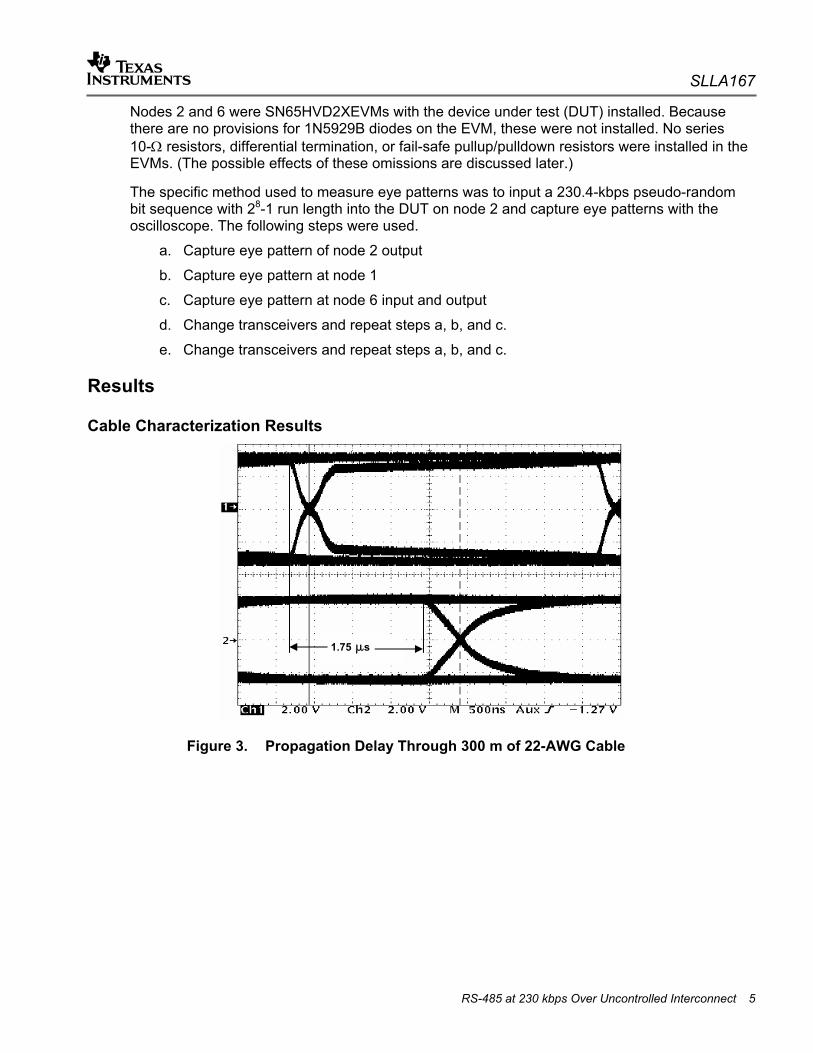
The specific method used to measure eye patterns was to input a 230.4-kbps pseudo-random bit sequence with 28-1 run length into the DUT on node 2 and capture eye patterns with the oscilloscope. The following steps were used.
a. Capture eye pattern of node 2 output
b. Capture eye pattern at node 1
c. Capture eye pattern at node 6 input and output
d. Change transceivers and repeat steps a, b, and c.
e. Change transceivers and repeat steps a, b, and c.
Results
Cable Characterization Results
Figure 3. Propagation Delay Through 300 m of 22-AWG Cable
1.75 µs

SLLA167
6 RS-485 at 230 kbps Over Uncontrolled Interconnect
Figure 4. Propagation Delay Through 300 m of 18-AWG Cable
Network Eye Patterns
Figure 5. MAX487 Driver Output at Node 2
1.67 µs

SLLA167
RS-485 at 230 kbps Over Uncontrolled Interconnect 7
Figure 6. SN65LBC184 Driver Output at Node 2
Figure 7. SN65HVD22 Driver Output at Node 2

SLLA167
8 RS-485 at 230 kbps Over Uncontrolled Interconnect
Figure 8. Node-1 Eye Pattern With MAX487 Driver at Node 2
Figure 9. Node-1 Eye Pattern With SN65LBC184 Driver at Node 2

SLLA167
RS-485 at 230 kbps Over Uncontrolled Interconnect 9
Figure 10. Node-1 Eye Pattern With SN65HVD22 Driver at Node 2
Figure 11. MAX487 Receiver Input and Output at Node 6

SLLA167
10 RS-485 at 230 kbps Over Uncontrolled Interconnect
Figure 12. SN65LBC184 Receiver Input and Output at Node 6
Figure 13. SN65HVD22 Receiver Input and Output at Node 6
SLLA167
RS-485 at 230 kbps Over Uncontrolled Interconnect 11
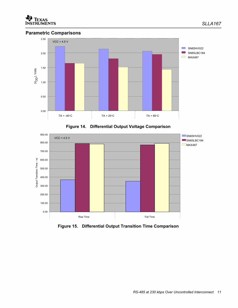
Parametric Comparisons
0.00
0.50
1.00
1.50
2.00
2.50
TA = -40°C TA = 25°C TA = 85°C
|VO
D|,
Vol
ts
SN65HV022SN65LBC184MAX487
VCC = 4.5 V
Figure 14. Differential Output Voltage Comparison
0.00
100.00
200.00
300.00
400.00
500.00
600.00
700.00
800.00
900.00 SN65HV022
MAX487
VCC = 4.5 VSN65LBC184
Rise Time Fall Time
Out
put T
rans
ition
Tim
e - n
s
Figure 15. Differential Output Transition Time Comparison

SLLA167
12 RS-485 at 230 kbps Over Uncontrolled Interconnect
0.00
10.00
20.00
30.00
40.00
50.00
60.00
70.00
80.00 SN65HV022
MAX487
VCC = 4.5 VSN65LBC184
TA = -40°C TA = 25°C TA = 85°C
Driv
er P
ulse
Ske
w -
ns
Figure 16. Driver Pulse Skew Comparison
0.00
10.00
20.00
30.00
40.00
50.00
60.00SN65HV022
MAX487
VCC = 4.5 VSN65LBC184
TA = -40°C TA = 25°C TA = 85°C
Rec
eive
Pul
se S
hew
- ns
Figure 17. Receiver Pulse Skew Comparison

SLLA167
RS-485 at 230 kbps Over Uncontrolled Interconnect 13
0
100
200
300
400
500
600
SN65HV022 MAX487SN65LBC184
TA = 25°CV
OD
(pp)
- mV
Figure 18. Peak-to-Peak Common-Mode Output Voltage Comparison
Discussion
Cables
As measured in Figure 3 and Figure 4, the propagation velocity of 22-AWG cable was 0.57c and the 18-AWG cable was 0.60c, where c is the speed of light in a vacuum or 3 x 10⁸ m/s. The high-frequency spectrum of the data signal takes longer to reach the end of the circuit in the 22-AWG cable than in the 18-AWG cable and ISI jitter is worse.
Because the delay measurements used a 100-Ω termination, the lack of noticeable reflections at the destination indicates the characteristic impedance of the 22-AWG cable to be near 100 Ω as is specified by the manufacturer.
The step of the destination signal from -3.2 V to about 2 V from a 6-V input step indicates a reflection coefficient of -0.133 and a characteristic impedance of approximately 76 Ω. This closely matches the manufacturers’ specification of 80 Ω.

SLLA167
14 RS-485 at 230 kbps Over Uncontrolled Interconnect
Eye Patterns
Not knowing the data sampling method or timing constraints, only the eye-pattern signal quality1 is used as a measure of good or bad. The two figures of merit extracted from the eye patterns in Figure 5 through Figure 13 are the differential noise margin and eye opening as a percentage of the unit interval.
Differential noise margin was measured from the smallest difference between the steady-state differential voltage or the minimum voltage after a slope reversal within the eye and a difference voltage of -200 mV or 200 mV. This is the difference voltage above the worst-case receiver input voltage threshold to be budgeted for external noise coupling or circuit parametric variability.
The time that the eye-pattern differential voltage is above 200 mV or below -200 mV was defined as the eye opening. This time divided by 4.34 µs times 100% gives the percentage of the unit interval that data is valid and may be sampled without error in this test setup. Conversely, 100% minus the eye opening gives the peak-to-peak jitter in the system.
The results of the eye-pattern analysis are in Table 1 and show that all scenarios maintain positive noise margin and greater than an 84% open eye. To help distinguish transceiver performance, Figure 19 plots the eye opening versus differential noise margin for each transceiver and connection scenario where best performance would be the largest noise margin and eye opening (up and right.)
Table 1. Summary of Eye-Pattern Measurements
Transceiver Figure Scenario Min Margin Open Eye Opening MAX487 5 0.55 V 4.1 µs 94% SN65LBC184 6 1.00 4.0 92% SN65HVD22 7
Driver Output at Node 2 0.40 4.1 95%
MAX487 8 2.10 3.9 90% SN65LBC184 9 2.10 3.8 86% SN65HVD22 10
Bus Signal at Node 1 3.20 4.0 93%
MAX487 11a Receiver Input at Node 6 1.80 3.6 84% MAX487 11b Receiver Output at Node 6 Not applicable 4.2 97% SN65LBC184 12a Receiver Input at Node 6 2.20 3.9 89% SN65LBC184 12b Receiver Output at Node 6 Not applicable 4.1 93% SN65HVD22 13a Receiver Input at Node 6 2.00 4.0 91% SN65HVD22 13b Receiver Output at Node 6 Not applicable 4.3 98%
1 For more information on eye patterns, see Interface Circuits for TIA/EIA-485 (RS-485) (SLLA036).

SLLA167
RS-485 at 230 kbps Over Uncontrolled Interconnect 15
Eye Opening versus Minimum Differential Noise Margin
MAX487
MAX487
MAX487
SN65LBC184
SN65LBC184
SN65LBC184
SN65HVD22
SN65HVD22
SN65HVD22
82%
84%
86%
88%
90%
92%
94%
96%
0 0.5 1 1.5 2 2.5 3 3.5
Differential Noise Margin, V
Eye
Ope
ning
Figure 19. Graphical Summary of Eye-Pattern Measurements
The minimum noise margin occurred for the SN65HVD22 and MAX487 at their output on node 2. Referring to Figure 5, Figure 6, and Figure 7, all transceivers show similar patterns with a voltage slope reversal and minimum occurring about 1.2 µs into the eye. This can only be the result of a return reflection from impedance discontinuity with a negative reflection coefficient. From Figure 1 and using a lossless transmission line model, it is apparent that nodes 1 and 3 present less than 100 Ω at the end of the transmission line from node 2 and are the likely causes of the decrease in noise margin. Confidence in this conclusion comes from the fact that the round-trip delay from node 2 to node 1 is about 1.1 µs and to node 3 is 1.5 µs.
Because the impedance discontinuity is the same for all cases, the difference in noise margin can only be attributed to the line driver characteristics. If the voltage step at time zero and at the source is vi(0), the voltage at the source a round-trip delay later is:
vi(t=2T)= vi(t=0-) + vi(0)(1 + (1 + pL) x (1 + ps)) (1)
Where:
pL is the reflection coefficient at the load
ps is the reflection coefficient at the source
T is the one-way delay

SLLA167
16 RS-485 at 230 kbps Over Uncontrolled Interconnect
vi(t=0-) is the initial differential bus voltage.
The variables determined by the driver are:
vi(t=0-), vi(0), and ps (2)
It is apparent from the voltage equation that a low initial voltage, a large voltage step, and negative and larger magnitude ps would increase the resultant voltage at the source. Unfortunately, these are not independent variables.
The lowest performance for eye opening occurred at the input to node 6 with the MAX487. As can be viewed in Figure 11, the input signal transition times are slow. (This is reasonable as this is the longest run in the network and, as Figure 14 and Figure 15 show, the MAX487 output is low and slow.) Because a ±200-mV threshold was used to measure the eye opening, a slower transition time will reduce the opening over faster transitions. This is evidenced by the more open eye generated by the faster SN65HVD22 driver in Figure 13.
Under these conditions, the receiver threshold is actually much closer to zero and explains the wider eye measured at the receiver output. However, a 0-V differential input voltage threshold cannot be ensured in practice and use of the worst-case receiver input voltage thresholds should be used to account for variability in this parameter.
Other Considerations Output voltage, transition times, and input thresholds and their relationship to signal quality have been discussed. Other factors to consider are pulse skew, which is a fixed component of the eye-pattern jitter, and the peak-to-peak common-mode output, which directly correlates to radiated emissions from the cable. Figure 16, Figure 17, and Figure 18 show these comparisons.
The 1N5929B zener diodes included in the customer’s design were omitted from this evaluation. These devices have a nominal reverse breakdown of 15 V, are unidirectional, have a working voltage of 11.4 V, and are rated at 3 W continuous and 98 W surge. The breakdown voltage is the same as the absolute maximum rating for the SN65LBC184 and above that of the MAX487 and affords little or no protection for those devices. Because it is unidirectional, the negative common-mode voltage range of this interface is limited to the forward voltage of the zener or -1.5 V and positive to 11.4 V. Because noise is generally bipolar, the ground potentials of each node in this network must be within 1.5 V of each other to communicate without error. Without these diodes, standard RS-485 devices would allow 7 V and the SN65HVD22 would allow 20 V of ground potential difference.
The series 10-Ω resistors were also omitted from the evaluation. The rationale for nondriving nodes has been presented and their effect on driving nodes will now be considered. These resistors increase the source resistance of the driver—lowering its initial voltage step between states and increasing the source reflection coefficient while having little effect on the steady-state output. All of these factors would reduce the noise margins measured here. The purpose of these resistors may be an attempt to protect the transceiver should the absolute maximum rating be exceeded. This can only happen if the MAX487 was used, or the 1N5929B fails. These would be of more use if located between the zener and the bus lines and would serve to protect the zener and not the transceivers.

SLLA167
RS-485 at 230 kbps Over Uncontrolled Interconnect 17
Pullup and pulldown 33-kΩ resistors were also omitted from this evaluation. Certainly, the resistance has little effect on the time-varying response of the circuit, as it is 330 times greater than the characteristic impedance of the cable. The differential steady-state bias produced from these and seven parallel 3.9-kΩ resistors across each node is approximately 40-mV bias and is inconsequential. This is likely too low to provide a reliable fail-safe bias under all operating conditions.
If the receiver output state is irrelevant when no input signal is present, then receiver input threshold hysteresis may be relied on to prevent oscillation of the output from differential noise on the bus. In this case, the SN65HVD22 data sheet specifies a minimum input hysteresis of 100 mV and a typical of 130 mV and is 60 mV greater than the typical 70 mV offered by both the SN65LBC184 and MAX487. All would be greater than the 40-mV fail-safe bias of the current design.
If the fail-safe receiver output state is relevant, then the SN65HVD22 provides a high-level output 250 µs after loss of signal with no external biasing or loss of differential noise margin. Ensuring a known output state with no input signal for the SN65LBC184 and MAX487 requires at least 200-mV differential bias and associated loss of differential noise margin
Summary and Conclusions While any of the candidate transceivers provide acceptable results in terms of signal quality in this evaluation, the reader is cautioned against inferring that this will hold under all conditions a data interface circuit is likely to experience in application. Of particular concern are low differential noise margin, restricted common-mode voltage range, and variability of critical transceiver and network parameters.
In this example network, the SN65LBC184 provided better differential noise margin than the other candidates with all scenarios considered. It has an output resistance between that of the SN65HVD22 and MAX487 and provides a better match for this network. Due to the questionable value and margin sensitivity to output resistance from the driving node, the series 10-Ω resistors should not be used. The need for and implementation of fail-safe provisions should be reconsidered. The SN65HVD22 provides the least margin impact for fail-safe but must be evaluated against undisclosed system constraints.
The 1N5929B zener diodes should be removed from the design and, if deemed necessary, replaced with bidirectional (back-to-back) zener diodes to maintain symmetrical common-mode tolerance. The SN65LBC184 has these integrated with the transceiver and they have a higher surge power rating than the 1N5929Bs.
It is clear from the results that this is a distributed-parameter circuit and must be treated as such. Assurance of differential margin necessitates some knowledge or control of reflection coefficients in the network and, if this is not possible, a reduction in signaling rate.
References 1. Low-Power, Slew-Rate-Limited RS-485/RS-422 Transceivers data sheet, 19-0122; Rev 7;
6/03, Maxim Integrated Products 2. 1N5913B Series 3 Watt DO-41 Surmetic™ 30 Zener Voltage Regulators data sheet, On
Semiconductor, February 2002- Rev. 2 3. ECI Product #6031804BFT4 specification sheet, Electro Cables Ltd

SLLA167
18 RS-485 at 230 kbps Over Uncontrolled Interconnect
4. Category 5e IBDN Control Plus specification sheet, NORDX/CDT 5. Extended Common-Mode RS-485 Transceivers, SN65HVD20/2x Family data sheet
(SLLS552C), September 2003 6. Differential Transceiver with Transient Voltage Suppression, SN65LBC184 data sheet
(SLLS236E) April 2002 7. Interface Circuits for TIA/EIA-485 (RS-485) design notes (SLLA036B), June 2002.

SLLA167
RS-485 at 230 kbps Over Uncontrolled Interconnect 19
Appendix A. Supplemental Testing Additional testing was requested to investigate the effects of driver output impedance and node capacitance.
A.1 Method
1. Set up as before and documented in the test report.
2. Install a 10-Ω resistor in series with each IO line of the EVM at node 2 with whatever device is currently installed.
3. Drive and measure eye pattern at node 2 at 230.4 kbps.
4. Change differential capacitance for all equivalent node circuits to 210 pF.
5. Measure eye pattern at node 2, and input to node 6.
6. Remove equivalent load from node 1, replace EVM at node 2 with equivalent load, and install EVM at node 1.
7. Drive from node 1 and measure eye patterns at nodes 2 and 1.
A.2 Results
The SN65LBC184 was the last device installed and was used for additional testing.
Figure A-1. Eye Pattern at Node 2 (Upper) and Node 6 (Lower) Driven From Node 2 With 10-Ω Resistor in Series With Each Output of the SN65LBC184

SLLA167
20 RS-485 at 230 kbps Over Uncontrolled Interconnect
Figure A-2. Eye Patterns at Node 2 (Upper) and Node 6 (Lower) With Series Output Resistors, 210-pF Node Capacitance and Driven From Node 2
Figure A-3. Eye Pattern at Node 1 (Upper) and Node 6 (Lower) Driven From Node 1
A.3 Discussion
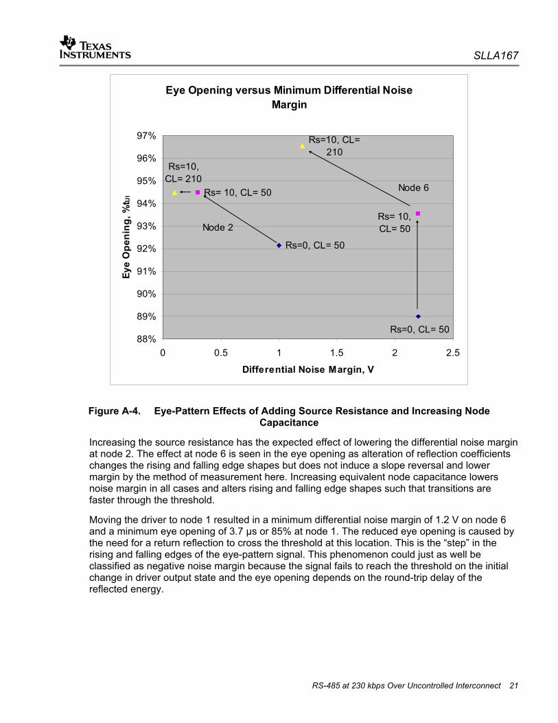
Installation of 10-Ω resistors in each output of the SN65LBC184 compares the eye patterns of Figure 6, Figure 12, and Figure A-1. Increasing the equivalent differential node capacitance to 210 pF on the six nodes not being driven and retaining the additional series output resistance give the eye patterns in Figure A-2 and is compared to Figure A-1 with equivalent node capacitance of 50 pF. Figure A-4 shows the differential noise margin and eye opening for these three scenarios.
SLLA167
RS-485 at 230 kbps Over Uncontrolled Interconnect 21
Eye Opening versus Minimum Differential Noise Margin
Rs=0, CL= 50
Rs= 10, CL= 50
Rs=10, CL= 210
Rs=0, CL= 50
Rs= 10, CL= 50
Rs=10, CL= 210
88%
89%
90%
91%
92%
93%
94%
95%
96%
97%
0 0.5 1 1.5 2 2.5
Differential Noise Margin, V
Eye
Ope
ning
, %t U
I
Node 6
Node 2
Figure A-4. Eye-Pattern Effects of Adding Source Resistance and Increasing Node Capacitance
Increasing the source resistance has the expected effect of lowering the differential noise margin at node 2. The effect at node 6 is seen in the eye opening as alteration of reflection coefficients changes the rising and falling edge shapes but does not induce a slope reversal and lower margin by the method of measurement here. Increasing equivalent node capacitance lowers noise margin in all cases and alters rising and falling edge shapes such that transitions are faster through the threshold.
Moving the driver to node 1 resulted in a minimum differential noise margin of 1.2 V on node 6 and a minimum eye opening of 3.7 µs or 85% at node 1. The reduced eye opening is caused by the need for a return reflection to cross the threshold at this location. This is the “step” in the rising and falling edges of the eye-pattern signal. This phenomenon could just as well be classified as negative noise margin because the signal fails to reach the threshold on the initial change in driver output state and the eye opening depends on the round-trip delay of the reflected energy.

SLLA167
22 RS-485 at 230 kbps Over Uncontrolled Interconnect
A.4 Summary and Conclusions
External resistors in series with the driver outputs and increasing node capacitance reduce differential noise margin. Both marginally improved the eye opening here but results depend on the bus configuration and may not be repeatable with other configurations.
Unless a benefit can be found for adding series resistors to the outputs, this is not recommended. This experiment is not overly sensitive to the equivalent differential node capacitance but, with the already low margin and unknowns, any reduction of differential noise margin is not recommended and node capacitance should be held to a minimum.

IMPORTANT NOTICE
Texas Instruments Incorporated and its subsidiaries (TI) reserve the right to make corrections, modifications,enhancements, improvements, and other changes to its products and services at any time and to discontinueany product or service without notice. Customers should obtain the latest relevant information before placingorders and should verify that such information is current and complete. All products are sold subject to TI’s termsand conditions of sale supplied at the time of order acknowledgment.
TI warrants performance of its hardware products to the specifications applicable at the time of sale inaccordance with TI’s standard warranty. Testing and other quality control techniques are used to the extent TIdeems necessary to support this warranty. Except where mandated by government requirements, testing of allparameters of each product is not necessarily performed.
TI assumes no liability for applications assistance or customer product design. Customers are responsible fortheir products and applications using TI components. To minimize the risks associated with customer productsand applications, customers should provide adequate design and operating safeguards.
TI does not warrant or represent that any license, either express or implied, is granted under any TI patent right,copyright, mask work right, or other TI intellectual property right relating to any combination, machine, or processin which TI products or services are used. Information published by TI regarding third-party products or servicesdoes not constitute a license from TI to use such products or services or a warranty or endorsement thereof.Use of such information may require a license from a third party under the patents or other intellectual propertyof the third party, or a license from TI under the patents or other intellectual property of TI.
Reproduction of information in TI data books or data sheets is permissible only if reproduction is withoutalteration and is accompanied by all associated warranties, conditions, limitations, and notices. Reproductionof this information with alteration is an unfair and deceptive business practice. TI is not responsible or liable forsuch altered documentation.
Resale of TI products or services with statements different from or beyond the parameters stated by TI for thatproduct or service voids all express and any implied warranties for the associated TI product or service andis an unfair and deceptive business practice. TI is not responsible or liable for any such statements.
Following are URLs where you can obtain information on other Texas Instruments products and applicationsolutions:
Products Applications
Amplifiers amplifier.ti.com Audio www.ti.com/audio
Data Converters dataconverter.ti.com Automotive www.ti.com/automotive
DSP dsp.ti.com Broadband www.ti.com/broadband
Interface interface.ti.com Digital Control www.ti.com/digitalcontrol
Logic logic.ti.com Military www.ti.com/military
Power Mgmt power.ti.com Optical Networking www.ti.com/opticalnetwork
Microcontrollers microcontroller.ti.com Security www.ti.com/security
Telephony www.ti.com/telephony
Video & Imaging www.ti.com/video
Wireless www.ti.com/wireless
Mailing Address: Texas Instruments
Post Office Box 655303 Dallas, Texas 75265
Copyright 2004, Texas Instruments Incorporated