r&s®smbv100a test & measurement data sheet | 01.01 … · pulse modulation (r&s ......
TRANSCRIPT

Test
& M
easu
rem
ent
Data
She
et |
01.0
1R&S®SMBV100A Vector Signal GeneratorSpecifications
Titel.indd 1 11.09.2008 14:47:11
2 R&S®SMBV100A Vector Signal Generator Version 01.01, September 2008
CONTENTS Key features .................................................................................................................................................................... 3 Specifications.................................................................................................................................................................. 4
RF characteristics ...................................................................................................................................................................................4 Frequency ...........................................................................................................................................................................................4 Frequency sweep ................................................................................................................................................................................4 Reference frequency ...........................................................................................................................................................................4 Level ....................................................................................................................................................................................................5 Level sweep ........................................................................................................................................................................................8 Spectral purity .....................................................................................................................................................................................8 List mode...........................................................................................................................................................................................11
Phase coherence (R&S®SMBV-B90 option) .........................................................................................................................................11 Analog modulation ................................................................................................................................................................................12
Possible modulation types.................................................................................................................................................................12 Simultaneous modulation ..................................................................................................................................................................12 Amplitude modulation........................................................................................................................................................................12 Frequency modulation.......................................................................................................................................................................13 Phase modulation..............................................................................................................................................................................14 Pulse modulation (R&S®SMBV-K22 option)......................................................................................................................................15 Input for external modulation signals.................................................................................................................................................15
Modulation sources...............................................................................................................................................................................15 Internal modulation generator ...........................................................................................................................................................15 Pulse generator (R&S®SMBV-K23 option) ........................................................................................................................................16
I/Q modulation.......................................................................................................................................................................................16 I/Q modulator.....................................................................................................................................................................................16 Internal baseband I/Q (with R&S®SMBV-B10/B50/B51 option).........................................................................................................17 I/Q outputs (with R&S®SMBV-B10/B50/B51 option)..........................................................................................................................17 I/Q baseband generator (R&S®SMBV-B10/50/51 option) – arbitrary waveform mode .....................................................................18 I/Q baseband generator (R&S®SMBV-B10 option) – realtime operation...........................................................................................20
Modulation performance for main standards ........................................................................................................................................22 Nominal values..................................................................................................................................................................................22
Modulation performance for digital standards.......................................................................................................................................23 Digital standards (for R&S®SMBV-B10) ......................................................................................................................26 Digital system with external PC software (for R&S®SMBV-B10/-B50/-B51) ............................................................ 26 Digital standards with R&S®WinIQSIM2™ (for R&S®SMBV-B10/-B50/-B51 ARB)................................................... 27 Additive white Gaussian noise (AWGN, R&S®SMBV-K62 option) ............................................................................ 27 General data .................................................................................................................................................................. 28
Remote control......................................................................................................................................................................................28 Operating data ......................................................................................................................................................................................28
Ordering information .................................................................................................................................................... 29 License information...................................................................................................................................................... 31

Version 01.01, September 2008 R&S®SMBV100A Vector Signal Generator 3
Key features
Ready for future applications today
• Future-proof hardware concept • RF section with high output level up to 6 GHz • Wide RF signal bandwidth of up to 120 MHz during internal signal generation • Maximum RF bandwidth of I/Q modulator exceeds 500 MHz • Always up-to-date with software upgrades
Customized internal signal generation with optional baseband
• Baseband coder with realtime capabilities for direct signal generation • Integrated ARB for playback of precalculated waveforms • Availability of ARB-only versions with different bandwidths • Memory depth of up to 256 Msample for long test sequences
Support of all important state-of-the-art digital standards
• Straightforward signal configuration due to easy-to-use GUI • 2G/3G/LTE mobile radio standards • Wireless standards incl. mobile WiMAX and WLAN IEEE 802.11n
High-performance RF for all kind of applications
• Excellent phase noise ensures low EVM with digital signals • High output level compensates for losses in the test/system setup • Fast settling time for quicker measurements • Analog modulation for basic measurements
Flexible signal processing and baseband connectivity
• CW interference and AWGN simulation • Analog and digital baseband outputs • Support for R&S®EX-IQ-Box digital interface adapter1
Low cost of ownership due to service concept
• Fast on-site servicing • Long calibration interval (three years) minimizes service costs • Straightforward modular design for short repair times
Allrounder and specialist at the same time
• Optimized for high production throughput − Multisegment waveform mode for fast switchover between test sequences − High level repeatability ensures stable test conditions
• Prepared for aerospace and defense applications − Versatile capabilities for generating unmodulated as well as complex modulated pulses − Coupling of multiple instruments for phase coherent RF generation
1 Available in January 2009.

4 R&S®SMBV100A Vector Signal Generator Version 01.01, September 2008
Specifications Specifications apply under the following conditions: 30 minutes warm-up time at ambient temperature, specified environmental conditions met, calibration cycle adhered to, and all internal automatic adjustments performed. "Typical values" are designated with the abbreviation "typ." These values are verified during the final test but are not assured by Rohde & Schwarz. "Nominal values" are design parameters that are not assured by Rohde & Schwarz. These values are verified during product development but are not specifically tested during production.
RF characteristics
Frequency R&S®SMBV-B103
CW mode 9 kHz to 3.2 GHz I/Q mode 1 MHz to 3.2 GHz
R&S®SMBV-B106 CW mode 9 kHz to 6 GHz
Range
I/Q mode 1 MHz to 6 GHz Resolution of setting 0.001 Hz Resolution of synthesis f = 1 GHz 0.44 µHz
to within <1 × 10⁻⁷ for f > 200 MHz or <20 Hz for f ≤ 200 MHz after IEC/IEEE bus delimiter
ALC state ON CW mode <3 ms I/Q mode <5 ms
ALC state Table <2 ms ALC state S&H <7 ms
Setting time
after trigger pulse in List mode2 <1 ms Phase offset adjustable in 0.1° steps
Frequency sweep Operating modes digital sweep in discrete steps automatic, step, single sweep,
external single, external step, manual or external trigger, linear or logarithmic spacing
Sweep range entire frequency range linear entire frequency range Step width logarithmic 0.01 % to 100 % per step setting range 10 ms to 10 s Dwell time resolution 0.1 ms
Reference frequency after 30 days of uninterrupted operation <1 × 10⁻⁶/year Aging with R&S®SMBV-B1 option <1 × 10⁻⁹/day, <1 × 10⁻⁷/year in temperature range 0 °C to 50 °C <2 × 10⁻⁶ Temperature effect with R&S®SMBV-B1 option <1 × 10⁻⁷
Warm-up time to nominal thermostat temperature (only with R&S®SMBV-B1 option)
≤10 min
frequency (approx. sinewave) 10 MHz level typ. 10 dBm
Output for internal reference signal
source impedance nominal 50 Ω frequency 10 MHz maximum deviation 3 × 10⁻⁶ input level, recommended ≥0 dBm, ≤16 dBm
Input for external reference
input impedance nominal 50 Ω
2 ALC state Sample & Hold or ALC state Table.
Version 01.01, September 2008 R&S®SMBV100A Vector Signal Generator 5
Level The R&S®SMBV100A has two different attenuator modes for level setting:
AUTO MODE: In this mode, the attenuator is switched automatically. The output level is specified over the entire range from –120 dBm to +13/+18 dBm.
FIXED MODE: The level is set without switching the attenuator. The attenuator is fixed to the current setting. If the ALC state is ON, level changes are performed without interruption. The maximum attenuation range is limited. With higher attenuation, the spectral purity of the output signal decreases.
The R&S®SMBV100A has four different automatic level control (ALC) modes:
ALC STATE AUTO: The best suited ALC mode is set automatically.
ALC STATE ON: The level control loop is closed. This mode is suitable for CW, AM and modulation signals with constant envelope.
ALC STATE SAMPLE & HOLD: At every frequency and level change, the level control loop is closed for about 1 ms and the level control voltage is sampled. The level control voltage is then clamped. This mode is used internally while in ALC state Auto for I/Q and pulse modulation.
ALC STATE TABLE: The level control voltage is obtained during a learning cycle as a function of level and frequency at discrete points. At normal operation the level control voltage is interpolated between the obtained values and set. This mode is suitable for I/Q and pulse modulation. The setting times are significantly faster than in the Sample & Hold mode, but the absolute level accuracy is slightly inferior due to the interpolation error and temperature changes after the learning cycle.
Setting range –145 dBm to +30 dBm 1 MHz ≤ f ≤ 6 GHz –120 dBm to +18 dBm (PEP) 3 Specified level range 200 kHz ≤ f < 1 MHz –120 dBm to +13 dBm (PEP)
Resolution 0.01 dB ALC state ON, Auto mode temperature range 18 °C to 33 °C
200 kHz ≤ f ≤ 3 GHz <0.5 dB
Absolute level error
f > 3 GHz <0.9 dB Additional level error ALC state Sample & Hold
ALC state Table <0.25 dB <0.5 dB
Output impedance VSWR in 50 Ω system 200 kHz ≤ f ≤ 6 GHz <1.8 after IEC/IEEE bus delimiter, with GUI update stopped, Auto mode, temperature range 18 °C to 33 °C, to <0.1 dB deviation from final value (unless otherwise stated)
ALC state ON CW mode <2.5 ms I/Q mode <5 ms
ALC state Table CW mode <2 ms I/Q mode4 <2 ms
ALC state S&H <7 ms in List mode after trigger pulse
CW mode <1 ms
Setting time
I/Q mode5 <1 ms Fixed mode, ALC state ON Uninterrupted level setting
setting range >20 dB maximum permissible RF power in output frequency range of RF path for f ≥ 1 MHz
1 MHz ≤ f ≤ 1 GHz 50 W 1 GHz < f ≤ 2 GHz 25 W 2 GHz < f ≤ 6 GHz 10 W
Reverse power (from ≥50 Ω source)
maximum permissible DC voltage 50 V
3 PEP = peak envelope power. 4 To <0.2 dB deviation from final value for frequencies <500 MHz and levels >+10 dBm. 5 ALC state Sample & Hold or ALC state Table; to <0.2 dB deviation from final value for frequencies <500 MHz and levels >+10 dBm.

6 R&S®SMBV100A Vector Signal Generator Version 01.01, September 2008
0 1 2 3 4 5 620
21
22
23
24
25
26
27
28
29
30
RF / GHz
Leve
l / d
Bm
CWI/Q
Measured maximum output power versus frequency
0 0.5 1 1.5 2 2.5 3 3.5 4 4.5 50
1000
2000
3000
4000
5000
6000
7000
8000
9000
10000
ALC = on
ALC = Table
ALC = Sample & Hold
List mode
Setting time [ms]
Occ
urre
nce
Histogram of measured level setting times in I/Q mode for different ALC states and List mode

Version 01.01, September 2008 R&S®SMBV100A Vector Signal Generator 7
Measured level repeatability 3GPP Test Model 1-64 at 2.16 GHz, 5 dBm, ALC=Table and ALC=Sample & Hold
8 R&S®SMBV100A Vector Signal Generator Version 01.01, September 2008
Level sweep Operating modes digital sweep in discrete steps automatic, step, single sweep,
external single, external step, manual or external trigger, linear spacing
entire level range Sweep range uninterrupted 0.1 dB to 20 dB
Step width 0.1 dB to 20 dB setting range 10 ms to 10 s Dwell time resolution 0.1 ms
Spectral purity f > 1 MHz Harmonics
level ≤ 8 dBm <–30 dBc 6 level >–10 dBm, >10 kHz carrier offset CW, I/Q mode (full-scale DC input)
f ≤ 1500 MHz <–70 dBc (typ. <–85 dBc) 1500 MHz < f ≤ 3 GHz <–64 dBc (typ. <–79 dBc)
Nonharmonics
f > 3 GHz <–58 dBc (typ. <–73 dBc) Wideband noise attenuator mode Auto
for level > 5 dBm >10 MHz carrier offset 1 Hz measurement bandwidth, CW
<–142 dBc (typ. –152 dBc)
20 kHz carrier offset, 1 Hz measurement bandwidth
f = 100 MHz CW mode <–141 dBc (typ. –147 dBc) I/Q mode <–121 dBc (typ. –126 dBc)
f = 1 GHz <–122 dBc (typ. –128 dBc) f = 2 GHz <–116 dBc (typ. –122 dBc) f = 3 GHz <–112 dBc (typ. –118 dBc) f = 4 GHz <–110 dBc (typ. –116 dBc)
SSB phase noise
f = 6 GHz <–106 dBc (typ. –112 dBc) f = 1 GHz, BW = 1 Hz to 10 MHz, CW with R&S®SMBV-B1 option
nominal 1.1 ps (1.1 mUI)
f = 1 GHz, BW = 1 Hz to 10 MHz, CW nominal 3.9 ps (3.9 mUI) f = 155 MHz, BW = 100 Hz to 1.5 MHz, CW
nominal 83 fs (12.9 µUI)
f = 622 MHz, BW = 1 kHz to 5 MHz, CW nominal 63 fs (39.2 µUI)
RMS jitter
f = 2.488 GHz, BW = 5 kHz to 15 MHz, CW
nominal 55 fs (137 µUI)
RMS value at f = 1 GHz, CW 0.3 kHz to 3 kHz, weighted (ITU-T) <4 Hz
Residual FM
0.03 kHz to 23 kHz <10 Hz Residual AM RMS value (0.03 kHz to 20 kHz), CW <0.02 %
6 Not valid in I/Q wideband mode.
Version 01.01, September 2008 R&S®SMBV100A Vector Signal Generator 9
0 1 2 3 4 5 6-90
-80
-70
-60
-50
-40
-30
Har
mon
ic /
dBc
Frequency / GHz
2*f3*f4*f
Measured harmonics at +18 dBm versus frequency
10 R&S®SMBV100A Vector Signal Generator Version 01.01, September 2008
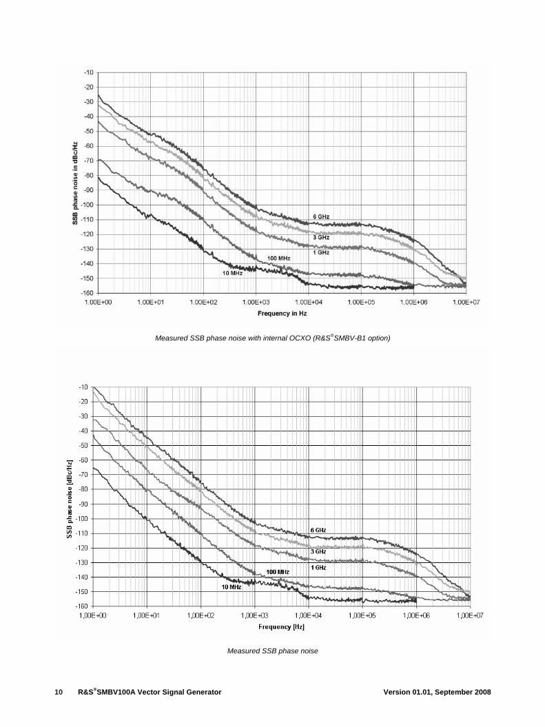
Measured SSB phase noise with internal OCXO (R&S®SMBV-B1 option)
Measured SSB phase noise
Version 01.01, September 2008 R&S®SMBV100A Vector Signal Generator 11
10 MHz 100 MHz 1 GHz 6 GHz-160
-155
-150
-145
-140
-135
-130
-125
-120
-115
-110
Carrier frequency
SS
B p
hase
noi
se [d
Bc/
Hz]
CWI/Q
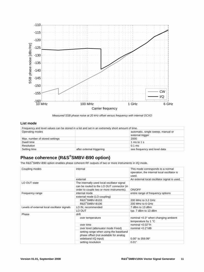
Measured SSB phase noise at 20 kHz offset versus frequency with internal OCXO
List mode Frequency and level values can be stored in a list and set in an extremely short amount of time. Operating modes automatic, single sweep, manual or
external trigger Max. number of stored settings 2000 Dwell time 1 ms to 1 s Resolution 0.1 ms Setting time after external triggering see frequency and level data
Phase coherence (R&S®SMBV-B90 option) The R&S®SMBV-B90 option enables phase coherent RF outputs of two or more instruments in I/Q mode.
internal This mode corresponds to a normal operation, the internal local oscillator is used.
Coupling modes
external An external local oscillator signal is used. LO OUT state The internally used local oscillator signal
can be routed to the LO OUT connector (in order to couple two or more instruments).
ON/OFF
internal mode entire range of frequency options external mode (LO coupling)
R&S®SMBV-B103 200 MHz to 3.2 GHz
Frequency range
R&S®SMBV-B106 200 MHz to 6 GHz LO IN, recommended 7 dBm to 13 dBm Levels of external local oscillator signals LO OUT typ. 7 dBm to 13 dBm drift
over temperature nominal <0.3° when changing ambient temperature by 1 °C
over time nominal <0.02°/h over level (attenuator mode Fixed) nominal <0.2°/dB setting range when using the baseband phase offset (not available for analog wideband I/Q input)
0.00° to 359.99°
Phase
setting resolution 0.01°
12 R&S®SMBV100A Vector Signal Generator Version 01.01, September 2008
Analog modulation
Possible modulation types I/Q modulation, amplitude modulation, frequency modulation, phase modulation, pulse modulation
Simultaneous modulation Amplitude
modulation Frequency modulation
Phase modulation Pulse modulation I/Q modulation
Amplitude modulation + + (+) – Frequency modulation + – + + Phase modulation + – + + Pulse modulation (+) + + + I/Q modulation – + + +
+ = compatible, – = incompatible, (+) = compatible with reduced AM modulation performance
Amplitude modulation For f ≥ 100 kHz, attenuator mode AUTO, level (PEP) within specified level range.
Operating modes internal, external, internal + external, AC/DC
Modulation depth At high levels, modulation is clipped when the maximum PEP is reached.
0 % to 100 %
Resolution 0.1 % fmod = 1 kHz and m <80 %
f ≤ 23.4375 MHz <(1 % of setting + 1 %) AM depth error
f > 23.4375 MHz <(4 % of setting + 1 %) fmod = 1 kHz, f ≤ 23.4375 MHz
m = 30 % <0.25 % m = 80 % <0.5 %
fmod = 1 kHz, f > 23.4375 MHz m = 30 % <1.5 %
AM distortion
m = 80 % <3 % Modulation frequency response m = 60 %, up to 50 kHz <3 dB Synchronous φM at AM m = 30 %, fmod = 1 kHz, ±peak/2 <0.2 rad

Version 01.01, September 2008 R&S®SMBV100A Vector Signal Generator 13
Frequency modulation f ≤ 23.4375 MHz rm = 1/4 23.4375 MHz < f ≤ 46.875 MHz rm = 1/32 46.875 MHz < f ≤ 93.75 MHz rm = 1/16 93.75 MHz < f ≤ 187.5 MHz rm = 1/8 187.5 MHz < f ≤ 375 MHz rm = 1/4 375 MHz < f ≤ 750 MHz rm = 1/2 750 MHz < f ≤ 1500 MHz rm = 1 1500 MHz < f ≤ 3 GHz rm = 2
FM multiplier for different frequency ranges
f > 3 GHz rm = 4 Operating modes internal, external, internal + external,
AC/DC, FM mode Low Noise, FM mode Normal, FM mode High Deviation
f ≤ 23.4375 MHz 1 MHz f > 23.4375 MHz
FM mode Normal rm × 2 MHz FM mode Low Noise rm × 1 MHz
Maximum deviation
FM mode High Deviation rm × 4 MHz Resolution <0.02 % of set deviation
min. rm × 0.1 Hz fmod = 1 kHz, deviation ≤ rm × 1 MHz
internal <(2 % of setting + 20 Hz) FM deviation error
external <(3 % of setting + 20 Hz) FM distortion fmod = 2 kHz, deviation = rm × 1 MHz <0.2 %
FM modes Low Noise and High Deviation DC/10 Hz to 100 kHz <3 dB
FM mode Normal
Modulation frequency response
DC/10 Hz to 500 kHz <3 dB Synchronous AM with FM 40 kHz deviation, fmod = 1 kHz, f > 10 MHz <0.2 % Carrier frequency offset with FM DC after FM offset calibration <0.2 % of set deviation
Max
imum
FM
dev
iatio
n
Frequency / MHz
0.009 23.4375 46.875 93.75 187.5 375 750 1500 3000 6000
31.25 kHz
62.5 kHz
125 kHz
250 kHz
500 kHz
1 MHz
2 MHz
4 MHz
8 MHz
16 MHz High DeviationNormalLow Noise
FM deviation versus frequency and operating mode

14 R&S®SMBV100A Vector Signal Generator Version 01.01, September 2008
Phase modulation f ≤ 23.4375 MHz rm = 1/4 23.4375 MHz < f ≤ 46.875 MHz rm = 1/32 46.875 MHz < f ≤ 93.75 MHz rm = 1/16 93.75 MHz < f ≤ 187.5 MHz rm = 1/8 187.5 MHz < f ≤ 375 MHz rm = 1/4 375 MHz < f ≤ 750 MHz rm = 1/2 750 MHz < f ≤ 1500 MHz rm = 1 1500 MHz < f ≤ 3 GHz rm = 2
φM multiplier for different frequency ranges
f > 3 GHz rm = 4 Operating modes internal, external, internal + external,
AC/DC, φM mode Low Noise, φM mode Normal, φM mode High Deviation
f ≤ 23.4375 MHz 2 rad f > 23.4375 MHz
φM mode Normal rm × 4 rad φM mode Low Noise rm × 10 rad
Maximum deviation
φM mode High Deviation rm × 40 rad Resolution <0.02 % of set deviation,
min. rm × 20 µrad fmod = 1 kHz, deviation ≤ half of max. deviation
internal <(2 % of setting + 0.003 rad)
φM deviation error
external <(3 % of setting + 0.003 rad) Distortion fmod = 10 kHz, half of max. deviation <0.2 %
φM modes Low Noise and High Deviation DC/10 Hz to 100 kHz <3 dB
φM mode Normal
Modulation frequency response
DC/10 Hz to 500 kHz <3 dB
Max
imum
PM
dev
iatio
n
Frequency / MHz
0.009 23.4375 46.875 93.75 187.5 375 750 1500 3000 6000
0.125 rad
0.25 rad0.3125 rad
0.5 rad0.625 rad
1 rad1.25 rad
2 rad2.5 rad
4 rad5 rad
8 rad10 rad
16 rad20 rad
40 rad
80 rad
160 radHigh DeviationNormalLow Noise
φM deviation versus frequency and operating mode

Version 01.01, September 2008 R&S®SMBV100A Vector Signal Generator 15
Pulse modulation (R&S®SMBV-K22 option) When pulse modulation is activated, the ALC state of the R&S®SMBV100A is automatically changed to ALC OFF (Sample & Hold). In this state, the ALC loop is opened and the output level is set directly. In order to set the correct output level, a Sample & Hold measurement is performed after each frequency or level setting.
Operating modes external, internal ON/OFF ratio >80 dB Rise/fall time 10 % to 90 % of RF amplitude <20 ns, typ. 4 ns Pulse repetition frequency 0 Hz to 2.5 MHz Video crosstalk spectral line of fundamental of 100 kHz
squarewave modulation <–30 dBc
Input for external modulation signals nominal input impedance >100 kΩ input sensitivity (peak value for set modulation depth or deviation)
nominal 1 V
Modulation input EXT for AM/FM/φM
maximum permissible input voltage ±10 V nominal input level
low threshold 0.5 V high threshold 1.5 V
maximum permissible input voltage ±5 V nominal input impedance >5 kΩ or 50 Ω
Modulation input PULSE
polarity selectable
Modulation sources
Internal modulation generator Waveforms sine, square
sine 0.1 Hz to 1 MHz Frequency range square 0.1 Hz to 20 kHz
Resolution of setting 0.1 Hz Frequency error <(0.005 Hz + relative error of reference
frequency × modulation frequency) sine Frequency response
0.1 Hz to 1 MHz <1 dB sine Distortion
f < 100 kHz at RL > 200 Ω, level (VEMF) < 1 V
<0.1 %
Vp at LF connector, open circuit voltage EMF
1 mV to 3 V
resolution 1 mV
Output voltage
setting error at 1 kHz <(1 % of setting + 1 mV) Output impedance nominal 10 Ω Frequency setting time to within <1 × 10⁻⁷, after IEC/IEEE bus
delimiter <5 ms
digital sweep in discrete steps operating modes automatic, step, single sweep,
external single, external step, manual or external trigger, linear or logarithmic spacing
sweep range entire frequency range step width (lin) entire frequency range
Sweep
step width (log) 0.01 % to 100 % per step

16 R&S®SMBV100A Vector Signal Generator Version 01.01, September 2008
Pulse generator (R&S®SMBV-K23 option) The pulse generator is fully digitally implemented; the clock is directly derived from the instrument’s reference frequency
Operating modes automatic, external trigger, external gate, single pulse, double pulse, delayed pulse (external trigger)
Active trigger edge positive or negative range 40 ns to 85 s Pulse period settings resolution 10 ns The pulse width of double pulses can be set independently.
range 10 ns to 1 s
Pulse width settings
resolution 10 ns range 10 ns to 1 s Pulse delay settings resolution 10 ns range 20 ns to 1 s Double-pulse spacing settings resolution 10 ns delay nominal 50 ns External trigger jitter of delay <10 ns
PULSE/VIDEO output LVTTL signal (RL ≥ 50 Ω)
I/Q modulation
I/Q modulator Operating modes external I/Q, internal I/Q
I offset, Q offset setting range –10 % to +10 % resolution 0.05 %
gain imbalance setting range –1.0 dB to +1.0 dB resolution 0.01 dB
quadrature offset setting range –8° to +8°
I/Q impairments
resolution 0.05° up to ±264 MHz at 3432 MHz, 3960 MHz and 4488 MHz
nominal <6 dB
up to ±60 MHz <6 dB up to ±10 MHz <2 dB
RF frequency response for entire instrument in modulation bandwidth
up to ±5 MHz <1 dB Carrier leakage without input signal, referenced to full-
scale input 7 <–50 dBc, typ. < –65 dBc
up to ±10 MHz nominal 40 dB Suppression of image sideband for entire instrument in modulation bandwidth up to ±60 MHz nominal 30 dB
input impedance nominal 50 Ω VSWR up to 60 MHz <1.2
External I/Q inputs
nominal input voltage for full-scale input q
2 2i + = 0.5 VV V
measured with 16QAM, filter root cosine α = 0.5, symbol rate 10 kHz rms value
f ≤ 200 MHz <0.6 % f > 200 MHz <(0.4 % + 0.2 % × f/GHz)
peak value f ≤ 200 MHz <1.2 %
Error vector
f > 200 MHz <(0.8 % + 0.4 % × f/GHz) test model 1, 64 DPCHs level ≤ 13 dBm PEP frequency 1800 MHz to 2200 MHz
offset 5 MHz >65 dB, typ. 67 dB
3GPP FDD digital standard, adjacent-channel leakage ratio (ACLR)
offset 10 MHz >67 dB, typ. 69 dB
7 Value applies after internal readjustment.

Version 01.01, September 2008 R&S®SMBV100A Vector Signal Generator 17
Internal baseband I/Q (with R&S®SMBV-B10/B50/B51 option) R&S®SMBV-B10/B50 400 Hz to 150 MHz Sample rate R&S®SMBV-B51 400 Hz to 90 MHz R&S®SMBV-B10/B50 nominal 120 MHz Bandwidth (RF) R&S®SMBV-B51 nominal 60 MHz
D/A converter resolution 16 bit with amplitude, group-delay and Si correction
bandwidth (drop to –0.1 dB) nominal 60 MHz D/A converter interpolation spectra
up to 10 MHz <–80 dBc
Aliasing filter
up to 60 MHz <–60 dBc I offset , Q offset
setting range –10 % to +10 % resolution 0.01 %
gain imbalance setting range –1 dB to +1 dB resolution 0.001 dB
quadrature offset setting range –10° to +10°
I/Q impairments
resolution 0.01°
I/Q outputs (with R&S®SMBV-B10/B50/B51 option) single-ended nominal 50 Ω Output impedance differential nominal 100 Ω EMF (output voltage depends on set modulation signal)
single-ended setting range 20 mV to 1.50 V (Vp) resolution 1 mV
differential setting range 40 mV to 3.00 V (Vp)
Output voltage
resolution 1 mV Offset EMF <1.0 mV
at RL = 50 Ω, (referenced to 1 MHz) magnitude
up to 10 MHz <0.15 dB up to 30 MHz (R&S®SMBV-B51) <0.3 dB up to 60 MHz (R&S®SMBV-B10/B50) <0.3 dB
nonlinear phase up to 10 MHz nominal 200 ps up to 30 MHz (R&S®SMBV-B51) nominal 500 ps
Frequency response
up to 60 MHz (R&S®SMBV-B10/B50) nominal 500 ps at RL = 50 Ω magnitude
up to 10 MHz <0.05 dB up to 30 MHz (R&S®SMBV-B51) <0.15 dB up to 60 MHz (R&S®SMBV-B10/B50) <0.15 dB
nonlinear phase up to 10 MHz nominal 100 ps up to 30 MHz (R&S®SMBV-B51) nominal 300 ps
I/Q imbalance 8
up to 60 MHz (R&S®SMBV-B10/B50) nominal 300 ps SFDR (sine)
up to 2 MHz >70 dB up to 20 MHz typ. 60 dB
phase noise 10 MHz sinewave at 20 kHz offset nominal –135 dBc
wideband noise
Spectral purity
10 MHz sinewave at 1 MHz offset nominal –145 dBc
8 Mode “Optimize internal I/Q impairments for RF output” is switched OFF.

18 R&S®SMBV100A Vector Signal Generator Version 01.01, September 2008
I/Q baseband generator (R&S®SMBV-B10/50/51 option) – arbitrary waveform mode output memory
waveform length 1 sample to 32 Msample in one-sample steps
waveform length with R&S®SMBV-B55 option
1 sample to 256 Msample in one-sample steps
resolution 16 bit loading time 1 Msample nominal 10 s
Waveform memory
nonvolatile memory hard disk, 80 Gbyte (with R&S®SMBV-B92 option)
setting range R&S®SMBV-B10/B50 400 Hz to 150 MHz R&S®SMBV-B51 400 Hz to 90 MHz
resolution 0.001 Hz clock source internal, external
Sample rate
frequency error (internal) < (5 × 10–14 + reference frequency error) × sample rate
The waveform is automatically interpolated to the internal 150 MHz sample rate.
bandwidth (drop to –0.1 dB) sample rate = 150 MHz (no interpolation)
nominal 60 MHz
sample rate < 150 MHz R&S®SMBV-B10 nominal 0.31 × sample rate
Interpolation
R&S®SMBV-B50/51 nominal 0.33 × sample rate With the aid of the frequency offset, the center frequency of the wanted baseband signal can be shifted. The restrictions caused by the modulation bandwidth apply.
setting range R&S®SMBV-B10/B50 –60 MHz to 60 MHz R&S®SMBV-B51 –30 MHz to 30 MHz
resolution 0.01 Hz
Frequency offset
frequency error <(5 × 10⁻¹⁰ + reference frequency error) × frequency offset
A trigger event restarts the I/Q generation. The I/Q signal is then synchronous with the trigger (with a specific timing jitter).
source internal, external operating modes Auto, Retrig, Armed Auto, Armed Retrig,
Single, Next external trigger delay (in sample)
setting range 0 to (216 – 1) resolution 0.01 jitter nominal ±3.3 ns
external trigger inhibit (in sample) setting range 0 to (226 – 1) resolution 1
Triggering
external trigger pulse width nominal >20 ns number 2 level LVTTL operating modes unchanged, restart, pulse, pattern, ratio,
trigger marker delay (in sample)
setting range 0 to (waveform length – 1) setting range without recalculation 0 to 2000
Marker outputs
resolution of setting 1

Version 01.01, September 2008 R&S®SMBV100A Vector Signal Generator 19
number of segments max. 100 segments changeover modes GUI, remote control, external trigger extended trigger modes same segment, next segment, next
segment seamless changeover time at 50 MHz clock rate (external trigger, without clock change)
nominal 5 µs
Multisegment waveform
seamless changeover output up to end of current segment, followed by changeover to next segment
number of carriers max. 32 carrier spacing
setting range depends on number of carriers and bandwidth (RF)
resolution 0.01 Hz crest factor modes maximize, minimize, OFF signal period modes longest file, shortest file, user (max. 1 s) single carrier gain
setting range –80 dB to 0 dB resolution 0.01 dB
single carrier start phase setting range 0° to 360° resolution 0.01°
single carrier delay setting range 0 s to 1 s
Multicarrier waveform
resolution 1 ns Operation with R&S®WinIQSIM2™: The software supports download of I/Q data and control of the R&S®SMBV-B10/50/51.
20 R&S®SMBV100A Vector Signal Generator Version 01.01, September 2008
I/Q baseband generator (R&S®SMBV-B10 option) – realtime operation ASK
modulation index 0 to 100 % resolution 0.1 %
FSK 2FSK, 4FSK, MSK deviation 0.1 to 1.5 × fSym maximum 10 MHz resolution 0.1 Hz
variable FSK 4FSK, 8FSK, 16FSK deviations –1.5 × fsym to +1.5 × fsym maximum 10 MHz resolution 0.1 Hz
PSK BPSK, QPSK, QPSK 45° Offset, OQPSK, π/4-QPSK, π/2-DBPSK, π/4-DQPSK, π/8-D8PSK, 8PSK, 8PSK EDGE
Types of modulation
QAM 16QAM, 32QAM, 64QAM, 256QAM, 1024QAM
Coding Not all coding methods can be used with every type of modulation.
OFF, Differential, Diff. Phase, Diff. + Gray, Gray, GSM, NADC, PDC, PHS, TETRA, APCO25 (PSK), PWT, TFTS, INMARSAT, VDL, EDGE, APCO25(FSK), ICO, CDMA2000® 9, WCDMA
Any filter can be used with any type of modulation. The bandwidth of the modulation signal is max. 45 MHz.
cosine, root cosine filter parameter α 0.05 to 1.00
Gaussian filter parameter B × T 0.15 to 2.50
cdmaOne, cdmaOne+ equalizer cdmaOne705 kHz cdmaOne705 kHz+ equalizer CDMA2000® 3x APCO25 C4FM rectangular split phase
filter parameter B × T 0.15 to 2.5
Baseband filter
resolution of filter parameter 0.01 If an external clock is used, the applied data rate may deviate from the set clock rate by ±2 %.
clock source internal, external setting range
ASK, PSK and QAM 400 Hz to 50 MHz FSK 400 Hz to 40 MHz resolution 0.001 Hz
frequency error (internal) <(5 × 10–14 + reference frequency error) × symbol rate
external clock modes symbol, K × symbol clock divider K 1 to 64
Symbol rate
external clock rate max. 150 MHz
9 CDMA2000® is a registered trademark of the Telecommunications Industry Association (TIA – USA).

Version 01.01, September 2008 R&S®SMBV100A Vector Signal Generator 21
With the aid of the frequency offset, the center frequency of the modulation signal in the baseband can be shifted. The restrictions caused by the modulation bandwidth apply.
setting range –60 MHz to 60 MHz resolution 0.01 Hz
Frequency offset
frequency error <(5 × 10⁻¹⁰ + reference frequency error) × frequency offset
ALL 0, ALL 1 PRBS
sequence length 9, 11, 15, 16, 20, 21, 23 pattern
length 1 bit to 64 bit data lists
output memory 8 bit to 2 Gbit
Data sources
nonvolatile memory hard disk (with R&S®SMBV-B92 option )
A trigger event restarts the I/Q generation. The I/Q signal is then synchronous with the trigger (with a specific timing jitter).
source internal, external operating modes Auto, Retrig, Armed Auto, Armed Retrig,
Single, Next external trigger delay (in symbol)
setting range 0 to (216 – 1) resolution 0.01 jitter nominal ±3.3 ns
external trigger inhibit (in symbol) setting range 0 to (226 – 1) resolution 1
Triggering
external trigger pulse width nominal >20 ns number 2 level LVTTL operating modes control list, pulse, pattern, ratio, trigger marker delay (in symbol)
setting range 0 to 224 – 1 setting range without recalculation 0 to 2000
Marker outputs
resolution of setting 1 internal: The signal switches between nominal and reduced level (without edge shaping).
setting range 0 dB to 60 dB additional level error in case of reduction
up to 30 dB <1 dB
Level reduction
up to 50 dB <3 dB internal: The signal triggers the beginning of a power ramp. The positive edge starts power ramping from blank to full level, the negative edge ramping in the opposite direction from full level to blanking.
operating range rise/fall time
setting range 0.5 symbol to 8 symbol resolution ¼ symbol
Burst
ramp shape cosine, linear

22 R&S®SMBV100A Vector Signal Generator Version 01.01, September 2008
Input impedance can be set separately for the trigger and the clock inputs.
input impedance 1 kΩ, nominal 50 Ω trigger/clock threshold
setting range 0.00 V to 2.00 V
Trigger/clock inputs
resolution 0.01 V Clock output level LVTTL
modulation, filter, symbol rate and coding in line with standard
Predefined settings
standards Bluetooth, DECT, ETC, GSM, GSM/EDGE, NADC, PDC, PHS, TETRA, WCDMA 3GPP, TD-SCDMA, CDMA2000® Forward, CDMA 2000® Reverse, Worldspace, TFTS
Modulation errors deviation 0.2 to 0.7 × symbol rate Gaussian filter with B × T = 0.2 to 0.7
symbol rate up to 2 MHz nominal 0.4 %
Deviation error with 2FSK, 4FSK
symbol rate up to 10 MHz nominal 1.2 % Gaussian filter with B × T = 0.2 to 0.7 Phase error with MSK
bit rate up to 10 MHz nominal 0.3° cosine, root cosine filter with α = 0.2 to 0.7
symbol rate up to 5 MHz nominal 0.5 % EVM with QPSK, OQPSK, π/4-DQPSK, 8PSK, 16QAM, 32QAM, 64QAM
symbol rate up to 20 MHz nominal 2.0 %
Modulation performance for main standards
Nominal values WCDMA 3GPP WiMAX Standard GSM EDGE
1DPCH TM1-64 CDMA2000® IEEE
802.11a/g BW = 8.75 MHz
BW = 10 MHz
LTE
2400 MHzto
2485 MHz
Frequency 400 MHz to
2000 MHz
400 MHz to
2000 MHz
1800 MHz to
2200 MHz
1800 MHto
2200 MHz
800 MHz
5150 MHz to
5825 MHz
2304 MHz 5000 MHz 1800 MHzto
2200 MHz
EVM – 0.2 % 0.3 % 0.6 % 0.4 % 0.6 % 0.3 % 0.4 % 0.4 % Phase error 0.15° – – – – – – – – Adjacent channel power ratio (ACPR) in dB Channel spacing 200 kHz 200 kHz 5 MHz 5 MHz 30 kHz 20 MHz – – – In adjacent channel
–37 –38 –69 –67 –79 at
0.75 MHz
–42 – – –
In alternate channel
–71 –71 –74 –69 –91 at
1.98 MHz
–55 – – –
In 2nd alternate channel
–85 –85 – – – –56 – – –

Version 01.01, September 2008 R&S®SMBV100A Vector Signal Generator 23
Modulation performance for digital standards GSM/EDGE with R&S®SMBV-K40 option Burst ON/OFF ratio typ. 100 dB
MSK, Gaussian filter B × T = 0.3 rms <0.4°, typ. 0.15°
Phase error
peak <1.2°, typ. 0.4° Error vector magnitude 8PSK EDGE, Gaussian linearized filter,
rms <0.5 %, typ. 0.2 %
Values measured with 30 kHz resolution bandwidth, referenced to level in band center without power ramping.
level ≤ 18 dBm PEP frequency 400 MHz to 2000 MHz
200 kHz offset <–34 dB, typ. –37 dB 400 kHz offset <–66 dB, typ. –71 dB
Power density spectrum
600 kHz offset <–74 dB, typ. –85 dB 3GPP FDD with R&S®SMBV-K42 option Error vector magnitude 1 DPCH, rms <0.8 %, typ. 0.3 %
test model 1, 64 DPCH level ≤ 13 dBm PEP frequency 1800 MHz to 2200 MHz
offset 5 MHz >65 dB, typ. 67 dB
Adjacent channel leakage ratio (ACLR)
offset 10 MHz >67 dB, typ. 69 dB
Digital standard 3GPP FDD test model 1, 64 DPCHs ACLR

24 R&S®SMBV100A Vector Signal Generator Version 01.01, September 2008
Digital standard 3GPP FDD test model 1, 64 DPCHs, measured ACLR as function of carrier level at 2 GHz

Version 01.01, September 2008 R&S®SMBV100A Vector Signal Generator 25
Multicarrier CW with R&S®SMBV-K61 option up to 10 MHz nominal 0.7 dB RF frequency response up to 60 MHz nominal 2.0 dB up to 10 MHz nominal 40 dB Suppression of unwanted carriers up to 60 MHz nominal 30 dB
Example of multicarrier CW, with different carrier powers and some carriers switched off in the left half of the spectrum, measured with I/Q level 0.5 V

26 R&S®SMBV100A Vector Signal Generator Version 01.01, September 2008
Digital standards (for R&S®SMBV-B10)
GSM/EDGE digital standard R&S®SMBV-K40 option 3GPP FDD digital standard R&S®SMBV-K42 option 3GPP FDD enhanced BS/MS tests including HSDPA R&S®SMBV-K43 option 3GPP FDD enhanced BS/MS tests including HSUPA R&S®SMBV-K45 option CDMA2000® digital standard R&S®SMBV-K46 option 1xEV-DO digital standard R&S®SMBV-K47 option IEEE 802.11a/b/g digital standard R&S®SMBV-K48 option IEEE 802.16 WiMAX digital standard including IEEE 802.16e R&S®SMBV-K49 option TD-SCDMA (3GPP TDD LCR) digital standard R&S®SMBV-K50 option TD-SCDMA (3GPP TDD LCR) enhanced BS/MS tests including HSDPA R&S®SMBV-K51 option DVB-H digital standard R&S®SMBV-K52 option IEEE 802.11n digital standard R&S®SMBV-K54 option EUTRA/LTE digital standard R&S®SMBV-K55 option HSPA+ R&S®SMBV-K59 option Multicarrier CW signal generation R&S®SMBV-K61 option
The options are described in the Digital Standards data sheet (PD 5213.9434.22).
Digital system with external PC software (for R&S®SMBV-B10/-B50/-B51)
Pulse sequencer (external PC software) R&S®SMBV-K6 option
The option is described in the Digital Standards data sheet (PD 5213.9434.22).
Playback of XM Radio Waveforms 10 R&S®SMBV-K256 option Playback of HD Radio™ Waveforms 11 R&S®SMBV-K352 option
10 Signal generation requires waveforms from XM radio. 11 HD Radio™ is a proprietary trademark of iBiquity Digital Corp..

Version 01.01, September 2008 R&S®SMBV100A Vector Signal Generator 27
Digital standards with R&S®WinIQSIM2™ (for R&S®SMBV-B10/-B50/-B51 ARB) R&S®WinIQSIM2™ requires an external PC.
GSM/EDGE digital standard R&S®SMBV-K240 option 3GPP FDD digital standard R&S®SMBV-K242 option 3GPP FDD enhanced BS/MS tests including HSDPA R&S®SMBV-K243 option GPS digital standard R&S®SMBV-K244 option 3GPP FDD enhanced BS/MS tests including HSUPA R&S®SMBV-K245 option CDMA2000® digital standard R&S®SMBV-K246 option 1 × EV-DO digital standard R&S®SMBV-K247 option IEEE 802.11a/b/g digital standard R&S®SMBV-K248 option IEEE 802.16 WiMAX digital standard including IEEE 802.16e R&S®SMBV-K249 option TD-SCDMA (3GPP TDD LCR) digital standard R&S®SMBV-K250 option TD-SCDMA (3GPP TDD LCR) enhanced BS/MS tests including HSDPA R&S®SMBV-K251 option DVB-H digital standard R&S®SMBV-K252 option IEEE 802.11n digital standard R&S®SMBV-K254 option EUTRA/LTE digital standard R&S®SMBV-K255 option HSPA+ R&S®SMBV-K259 option Multicarrier CW signal generation R&S®SMBV-K261 option Additive white Gaussian noise (AWGN) R&S®SMBV-K262 option
The options are described in the R&S®WinIQSIM2™ data sheet (PD 5213.7460.22).
Additive white Gaussian noise (AWGN, R&S®SMBV-K62 option) As prerequisite, R&S®SMBV-B10/-B50/-B51 must be installed.
Addition of an AWGN signal of settable bandwidth and settable C/N ratio or Eb/N0 to a wanted signal. If the noise generator is used, a frequency offset cannot be added to the wanted signal.
distribution density Gaussian, statistical, separate for I and Q crest factor >18 dB
Noise
periodicity >48 h setting range –30 dB to +30 dB
resolution 0.1 dB C/N, Eb/N0
uncertainty for system bandwidth = symbol rate, symbol rate <4 MHz, –24 dB < C/N < 30 dB and crest factor <12 dB
<0.1 dB
bandwidth for determining noise power setting range
R&S®SMBV-B10/B50 R&S®SMBV-B51
1 kHz to 120 MHz 1 kHz to 60 MHz
System bandwidth
setting resolution 100 Hz

28 R&S®SMBV100A Vector Signal Generator Version 01.01, September 2008
General data Remote control Systems IEC/IEEE bus, IEC 60625 (IEEE 488)
Ethernet (TC/IP) USB
Command set SCPI 1999.5 Connector IEC
Ethernet USB
24-contact Amphenol Western slave
IEC/IEEE bus address 0 to 30 Interface functions SH1, AH1, T6, L4, SR1, RL1, PP1, DC1,
DT1, C0 LAN interface 10/100BaseT
Operating data input voltage range 100 V to 240 V (AC) ±10 % AC supply frequency 50 Hz to 60 Hz, –5 %/+10 %
Power supply, nominal values
max. input current 1.4 A (100 V) to 0.6 A (240 V) Power factor correction in line with EN 61000-3-2 EMC in line with EN 55011 class B, EN 61326 Immunity to interfering field strength up to 10 V/m
operating temperature range 0 °C to 55 °C in line with EN 60068-2-1, EN 60068-2-2
storage temperature range –40 °C to +71 °C climatic resistance, +40 °C/95 % rel. humidity
in line with EN 60068-2-78
Environmental conditions
operating altitude if equipped with SMBV-B92
up to 4600 m up to 3000 m
vibration, sinusoidal 5 Hz to 150 Hz, max. 2 g at 55 Hz, max. 0.5 g at 55 Hz to 150 Hz, in line with EN 60068-2-6
vibration, random 10 Hz to 300 Hz, acceleration 1.2 g (rms) in line with EN 60068-2-64
Mechanical resistance
shock 40 g shock spectrum in line with EN 60068-2-27, MIL-STD-810E
Electrical safety in line with IEC 61010-1, EN 61010-1, CAN/CSA-C22.2 No. 61010-1-04, UL 61010-1
Approvals VDE-GS, CCSAUS Dimensions (W × H × D) 344 mm × 112 mm × 368 mm
(13.54 in × 4.41 in × 14.49 in) Weight when fully equipped nominal 7.9 kg (17.4 lb) Recommended calibration interval 3 years
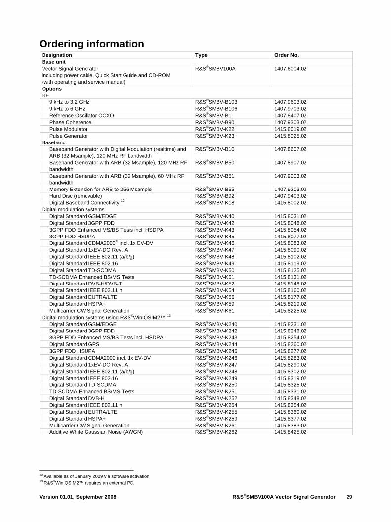
Version 01.01, September 2008 R&S®SMBV100A Vector Signal Generator 29
Ordering information Designation Type Order No. Base unit Vector Signal Generator including power cable, Quick Start Guide and CD-ROM (with operating and service manual)
R&S®SMBV100A 1407.6004.02
Options RF
9 kHz to 3.2 GHz R&S®SMBV-B103 1407.9603.02 9 kHz to 6 GHz R&S®SMBV-B106 1407.9703.02 Reference Oscillator OCXO R&S®SMBV-B1 1407.8407.02 Phase Coherence R&S®SMBV-B90 1407.9303.02 Pulse Modulator R&S®SMBV-K22 1415.8019.02 Pulse Generator R&S®SMBV-K23 1415.8025.02
Baseband Baseband Generator with Digital Modulation (realtime) and ARB (32 Msample), 120 MHz RF bandwidth
R&S®SMBV-B10 1407.8607.02
Baseband Generator with ARB (32 Msample), 120 MHz RF bandwidth
R&S®SMBV-B50 1407.8907.02
Baseband Generator with ARB (32 Msample), 60 MHz RF bandwidth
R&S®SMBV-B51 1407.9003.02
Memory Extension for ARB to 256 Msample R&S®SMBV-B55 1407.9203.02 Hard Disc (removable) R&S®SMBV-B92 1407.9403.02 Digital Baseband Connectivity 12 R&S®SMBV-K18 1415.8002.02
Digital modulation systems Digital Standard GSM/EDGE R&S®SMBV-K40 1415.8031.02 Digital Standard 3GPP FDD R&S®SMBV-K42 1415.8048.02 3GPP FDD Enhanced MS/BS Tests incl. HSDPA R&S®SMBV-K43 1415.8054.02 3GPP FDD HSUPA R&S®SMBV-K45 1415.8077.02 Digital Standard CDMA2000® incl. 1x EV-DV R&S®SMBV-K46 1415.8083.02 Digital Standard 1xEV-DO Rev. A R&S®SMBV-K47 1415.8090.02 Digital Standard IEEE 802.11 (a/b/g) R&S®SMBV-K48 1415.8102.02 Digital Standard IEEE 802.16 R&S®SMBV-K49 1415.8119.02 Digital Standard TD-SCDMA R&S®SMBV-K50 1415.8125.02 TD-SCDMA Enhanced BS/MS Tests R&S®SMBV-K51 1415.8131.02 Digital Standard DVB-H/DVB-T R&S®SMBV-K52 1415.8148.02 Digital Standard IEEE 802.11 n R&S®SMBV-K54 1415.8160.02 Digital Standard EUTRA/LTE R&S®SMBV-K55 1415.8177.02 Digital Standard HSPA+ R&S®SMBV-K59 1415.8219.02 Multicarrier CW Signal Generation R&S®SMBV-K61 1415.8225.02
Digital modulation systems using R&S®WinIQSIM2™ 13 Digital Standard GSM/EDGE R&S®SMBV-K240 1415.8231.02 Digital Standard 3GPP FDD R&S®SMBV-K242 1415.8248.02 3GPP FDD Enhanced MS/BS Tests incl. HSDPA R&S®SMBV-K243 1415.8254.02 Digital Standard GPS R&S®SMBV-K244 1415.8260.02 3GPP FDD HSUPA R&S®SMBV-K245 1415.8277.02 Digital Standard CDMA2000 incl. 1x EV-DV R&S®SMBV-K246 1415.8283.02 Digital Standard 1xEV-DO Rev. A R&S®SMBV-K247 1415.8290.02 Digital Standard IEEE 802.11 (a/b/g) R&S®SMBV-K248 1415.8302.02 Digital Standard IEEE 802.16 R&S®SMBV-K249 1415.8319.02 Digital Standard TD-SCDMA R&S®SMBV-K250 1415.8325.02 TD-SCDMA Enhanced BS/MS Tests R&S®SMBV-K251 1415.8331.02 Digital Standard DVB-H R&S®SMBV-K252 1415.8348.02 Digital Standard IEEE 802.11 n R&S®SMBV-K254 1415.8354.02 Digital Standard EUTRA/LTE R&S®SMBV-K255 1415.8360.02 Digital Standard HSPA+ R&S®SMBV-K259 1415.8377.02 Multicarrier CW Signal Generation R&S®SMBV-K261 1415.8383.02 Additive White Gaussian Noise (AWGN) R&S®SMBV-K262 1415.8425.02
12 Available as of January 2009 via software activation. 13 R&S®WinIQSIM2™ requires an external PC.

30 R&S®SMBV100A Vector Signal Generator Version 01.01, September 2008
Digital modulation systems using an external PC software or waveforms Pulse Sequencer 14 R&S®SMBV-K6 1415.8390.02 Playback of XM Radio Waveforms 15 R&S®SMBV-K256 1415.8402.02 Playback of HD Radio™ Waveforms R&S®SMBV-K352 1415.8431.02
Noise generation Additive White Gaussian Noise (AWGN) R&S®SMBV-K62 1415.8419.02
Recommended extras Hardcopy manuals (in English, UK) 1407.6062.32 Hardcopy manuals (in English, US) 1407.6062.39 19” Rack Adapter R&S®ZZA-S334 1109.4487.00 Power Sensor 9 kHz to 6 GHz R&S®NRP-Z92 1171.7005.02 Keyboard with USB Interface (US character set) R&S®PSL-Z2 1157.6870.04 Mouse with USB Interface, optical R&S®PSL-Z10 1157.7060.03
14 Pulse sequencer requires an external PC. 15 Signal generation requires waveforms from XM radio.

Version 01.01, September 2008 R&S®SMBV100A Vector Signal Generator 31
License information The firmware of this device contains open source software. Details as well as license agreements can be found in release notes and the operating manual.
Certified Environmental System
ISO 14001DQS REG. NO 1954 UM
Certified Quality System
ISO 9001DQS REG. NO 1954 QM
For product brochure, see PD 5214.1114.12
and www.rohde-schwarz.com
Service you can rely onJ In 70 countries J Person-to-personJ CustomizedandflexibleJ QualitywithawarrantyJ No hidden terms
Rohde & Schwarz GmbH & Co. KGMühldorfstraße15|81671MünchenPhone+498941290|Fax+4989412912164
www.rohde-schwarz.com
R&S®isaregisteredtrademarkofRohde&SchwarzGmbH&Co.KG Tradenamesaretrademarksoftheowners|PrintedinGermany(bb) PD5214.1114.22|Version01.01|September2008|R&S®SMBV100A Subject to change *0.14€/minwithinGermanwirelinenetwork;ratesmayvaryinothernetworks(wirelineandmobile)andcountries.
About Rohde & SchwarzRohde&Schwarzisanindependentgroupofcompaniesspecializinginelectronics.Itisaleadingsupplierofsolu-tionsinthefieldsoftestandmeasurement,broadcasting,radiomonitoringandradiolocation,aswellassecurecom-munications.Established75yearsago,Rohde&Schwarzhasaglobalpresenceandadedicatedservicenetworkinover70countries.CompanyheadquartersareinMunich,Germany.
Regional contactEurope,Africa,MiddleEast+491805124242*or+4989412913774customersupport@rohde-schwarz.comNorthAmerica1-888-TEST-RSA(1-888-837-8772)[email protected][email protected]/[email protected]
Titel.indd 2 11.09.2008 14:47:11