rx210 group datasheet - futureelectronics.com electronics... · r01ds0041ej0120 rev.1.20 page 1 of...
TRANSCRIPT
Datasheet
R01DS0041EJ0120 Rev.1.20 Page 1 of 162Nov 28, 2012
RX210 GroupRenesas MCUs
Features 32-bit RX CPU core Max. operating frequency: 50 MHz
Capable of 78 DMIPS in operation at 50 MHz Accumulator handles 64-bit results (for a single
instruction) from 32- × 32-bit operations Multiplication and division unit handles 32- × 32-bit
operations (multiplication instructions take one CPU clock cycle)
Fast interrupt CISC Harvard architecture with 5-stage pipeline Variable-length instructions, ultra-compact code On-chip debugging circuit
Low power design and architecture Operation from a single 1.62-V to 5.5-V supply 1.62-V operation available (at up to 20 MHz) Deep software standby mode with RTC remaining usable Four low power modes
On-chip flash memory for code, no wait states 50-MHz operation, 20-ns read cycle No wait states for reading at full CPU speed 64-K to 512-Kbyte capacities User code programmable via the SCI Programmable at 1.62 V For instructions and operands
On-chip data flash memory 8 Kbytes
(Number of times of reprogramming: 100,000) Erasing and programming impose no load on the CPU.
On-chip SRAM, no wait states 12-K to 64-Kbyte size capacities
DMA DMAC: Incorporates four channels DTC: Four transfer modes
ELC Module operation can be initiated by event signals
without going through interrupts. Modules can operate while the CPU is sleeping.
Reset and supply management Nine types of reset, including the power-on reset (POR) Low voltage detection (LVD) with voltage settings
Clock functions Frequency of external clock: Up to 20 MHz Frequency of the oscillator for sub-clock generation:
32.768 kHz PLL circuit input: 4 MHz to 12.5 MHz On-chip low- and high-speed oscillators, dedicated on-
chip low-speed oscillator for the IWDT Generation of a dedicated 32.768-kHz clock for the RTC Clock frequency accuracy measurement circuit (CAC)
Real-time clock Adjustment functions (30 seconds, leap year, and error) Time capture function Time capture on event-signal input through external pins RTC capable of initiating return from deep software
standby mode
Independent watchdog timer 125-kHz on-chip oscillator produces a dedicated clock
signal to drive IWDT operation.
Useful functions for IEC60730 compliance Self-diagnostic and disconnection-detection assistance
functions for the A/D converter, clock frequency accuracy measurement circuit, independent watchdog timer, functions to assist in RAM testing, etc.
Up to nine communications channels SCI with many useful functions (up to seven channels)
Asynchronous mode, clock synchronous mode, smart card interface
I2C bus interface: Transfer at up to 400 kbps, capable of SMBus operation (one channel)
RSPI (one channel)
External address space Four CS areas (4 × 16 Mbytes) 8- or 16-bit bus space is selectable per area
Up to 14 extended-function timers 16-bit MTU: input capture, output compare,
complementary PWM output, phase counting mode (six channels)
8-bit TMR (four channels) 16-bit compare-match timers (four channels)
12-bit A/D converter Capable of conversion within 1 μs Sample-and-hold circuits (for three channels) Three-channel synchronized sampling available Self-diagnostic function and analog input disconnection
detection assistance function
10-bit D/A converter
Analog comparator
General I/O ports 5-V tolerant, open drain, input pull-up, switching of
driving ability
MPC Multiple locations are selectable for I/O pins of
peripheral functions
Temperature sensor
Operating temp. range 40C to +85C 40C to +105C
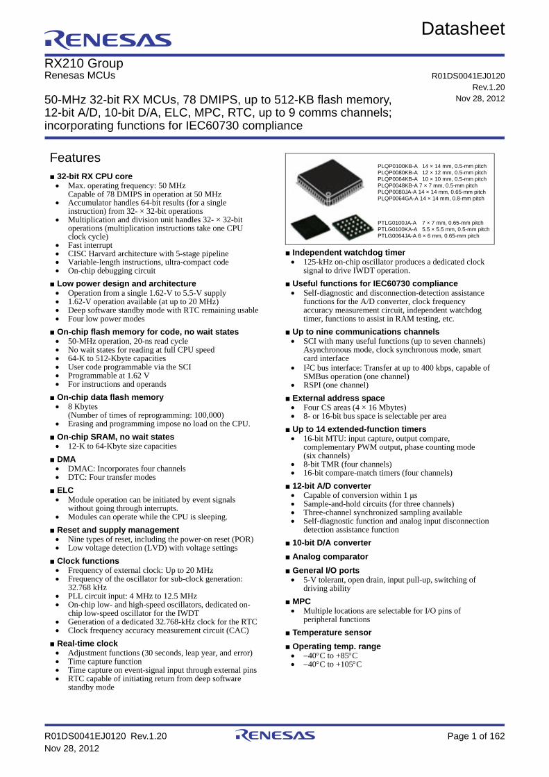
PLQP0100KB-A 14 × 14 mm, 0.5-mm pitchPLQP0080KB-A 12 × 12 mm, 0.5-mm pitchPLQP0064KB-A 10 × 10 mm, 0.5-mm pitchPLQP0048KB-A 7 × 7 mm, 0.5-mm pitchPLQP0080JA-A 14 × 14 mm, 0.65-mm pitchPLQP0064GA-A 14 × 14 mm, 0.8-mm pitch
PTLG0100JA-A 7 × 7 mm, 0.65-mm pitchPTLG0100KA-A 5.5 × 5.5 mm, 0.5-mm pitchPTLG0064JA-A 6 × 6 mm, 0.65-mm pitch
50-MHz 32-bit RX MCUs, 78 DMIPS, up to 512-KB flash memory, 12-bit A/D, 10-bit D/A, ELC, MPC, RTC, up to 9 comms channels; incorporating functions for IEC60730 compliance
R01DS0041EJ0120Rev.1.20
Nov 28, 2012

R01DS0041EJ0120 Rev.1.20 Page 2 of 162Nov 28, 2012
RX210 Group 1. Overview
1.Overview
1.1 Outline of Specifications
Table 1.1 lists the specifications in outline, and Table 1.2 gives a comparison of the functions of products in different
packages.
Table 1.1 is for products with the greatest number of functions, so numbers of peripheral modules and channels will
differ in accord with the package. For details, see Table 1.2, Comparison of Functions for Different Packages.
This product includes chip version A (part no.: R5F5210xAxxx), chip version B (part no.: R5F5210xBxxx), and chip
version C (part no: R5F5210xCxxx).
Table 1.1 Outline of Specifications (1 / 4)
Classification Module/Function Description
CPU CPU Maximum operating frequency: 50 MHz 32-bit RX CPU Minimum instruction execution time: One instruction per state (cycle of the system clock) Address space: 4-Gbyte linear Register
General purpose: Sixteen 32-bit registersControl: Eight 32-bit registersAccumulator: One 64-bit register
Basic instructions: 73 DSP instructions: 9 Addressing modes: 10 Data arrangement
Instructions: Little endianData: Selectable as little endian or big endian
On-chip 32-bit multiplier: 32 32 64 bits On-chip divider: 32 / 32 32 bits Barrel shifter: 32 bits
Memory ROM Capacity: 64 K/96 K/128 K/256 K/384 K/512 Kbytes 50 MHz, no-wait memory access On-board programming: 3 types
Off-board programming (parallel programmer mode)
RAM Capacity: 12 K/16 K/20 K/32 K/64 K Kbytes 50 MHz, no-wait memory access
E2 DataFlash Capacity: 8 Kbytes Number of times for programming/erasing: 100,000
MCU operating mode Single-chip mode, on-chip ROM enabled expansion mode, and on-chip ROM disabled expansion mode (software switching)
Clock Clock generation circuit Main clock oscillator, sub-clock oscillator, low-speed on-chip oscillator, high-speed on-chip oscillator, PLL frequency synthesizer, and IWDT-dedicated on-chip oscillator
Oscillation stop detection Measuring circuit for accuracy of clock frequency (clock-accuracy check: CAC) Independent settings for the system clock (ICLK), peripheral module clock (PCLK), external bus clock
(BCLK), and flashIF clock (FCLK)The CPU and system sections such as other bus masters run in synchronization with the system clock (ICLK): 50 MHz (at max.)Peripheral modules run in synchronization with the peripheral module clock (PCLK): 32 MHz (at max.)Devices connected to the external bus run in synchronization with the external bus clock (BCLK): 12.5 MHz (at max.) The flash peripheral circuit runs in synchronization with the flash peripheral clock (FCLK): 32 MHz (at max.)
Reset RES# pin reset, power-on reset, voltage monitoring reset, watchdog timer reset, independent watchdog timer reset, deep software standby reset, and software reset
Voltage detection Voltage detection circuit (LVDAa)
When the voltage on VCC falls below the voltage detection level, an internal reset or internal interrupt is generated.Voltage detection circuit 0 is capable of selecting the detection voltage from 4 levelsVoltage detection circuit 1 is capable of selecting the detection voltage from 16 levelsVoltage detection circuit 2 is capable of selecting the detection voltage from 16 levels
R01DS0041EJ0120 Rev.1.20 Page 3 of 162Nov 28, 2012
RX210 Group 1. Overview
Low power consumption
Low power consumption facilities
Module stop function Four low power consumption modes
Sleep mode, all-module clock stop mode, software standby mode, and deep software standby mode
Function for lower operating power consumption
Operating power control modes[Chip versions A and C]High-speed operating mode, middle-speed operating mode 1A, middle-speed operating mode 1B, low-speed operating mode 1, low-speed operating mode 2[Chip version B]High-speed operating mode, middle-speed operating mode 1A, middle-speed operating mode 1B, middle-speed operating mode 2A, middle-speed operating mode 2B, low-speed operating mode 1, low-speed operating mode 2
Interrupt Interrupt controller (ICUb) Interrupt vectors: 117 External interrupts: 9 (NMI, IRQ0 to IRQ7 pins) Non-maskable interrupts: 6 (the NMI pin, oscillation stop detection interrupt, voltage monitoring 1
interrupt, voltage monitoring 2 interrupt, WDT interrupt, and IWDT interrupt) 16 levels specifiable for the order of priority
External bus extension The external address space can be divided into four areas (CS0 to CS3), each with independent control of access settings. Capacity of each area: 16 Mbytes (CS0 to CS3) A chip-select signal (CS0# to CS3#) can be output for each area. Each area is specifiable as an 8-bit or 16-bit bus space The data arrangement in each area is selectable as little or big endian (only for data).Bus format: Separate bus, multiplex bus
Wait control Write buffer facility
DMA DMA controller (DMACA) 4 channels Three transfer modes: Normal transfer, repeat transfer, and block transfer Activation sources: Software trigger, external interrupts, and interrupt requests from peripheral
functions
Data transfer controller (DTCa)
Three transfer modes: Normal transfer, repeat transfer, and block transfer Activation sources: Interrupts Chain transfer function
I/O ports General I/O ports 100-pin/80-pin/64-pin/48-pin I/O pin: 84/64/48/34 Input: 1/1/1/1 Pull-up resistors: 84/64/48/34 Open-drain outputs: 54/44/35/26 5-V tolerance:4/4/2*1/2
Event link controller (ELC) Event signals of 59 types can be directly connected to the module Operations of timer modules are selectable at event input Capable of event link operation for ports B and E
Multi-function pin controller (MPC) Capable of selecting input/output function from multiple pins
Table 1.1 Outline of Specifications (2 / 4)
Classification Module/Function Description

R01DS0041EJ0120 Rev.1.20 Page 4 of 162Nov 28, 2012
RX210 Group 1. Overview
Timers Multi-function timer pulse unit 2 (MTU2a)
(16 bits 6 channels) 1 unit Time bases for the six 16-bit timer channels can be provided via up to 16 pulse-input/output lines and
three pulse-input lines Select from among eight or seven counter-input clock signals for each channel (PCLK/1, PCLK/4,
PCLK/16, PCLK/64, PCLK/256, PCLK/1024, MTCLKA, MTCLKB, MTCLKC, MTCLKD) other than channel 5, for which only four signals are available.
Input capture function 21 output compare/input capture registers Pulse output mode Complementary PWM output mode Reset synchronous PWM mode Phase-counting mode Generation of triggers for A/D converter conversion
Port output enable 2 (POE2a)
Controls the high-impedance state of the MTU’s waveform output pins
8-bit timer (TMR) (8 bits 2 channels) 2 units Select from among seven internal clock signals (PCLK1, PCLK/2, PCLK/8, PCLK/32, PCLK/64,
PCLK/1024, PCLK/8192) and one external clock signal Capable of output of pulse trains with desired duty cycles or of PWM signals The 2 channels of each unit can be cascaded to create a 16-bit timer Capable of generating baud-rate clocks for SCI5, SCI6, and SCI12
Compare match timer (CMT)
(16 bits 2 channels) 2 units Select from among four clock signals (PCLK/8, PCLK/32, PCLK/128, PCLK/512)
Watchdog timer (WDTA) 14 bits 1 channel Select from among 6 counter-input clock signals (PCLK/4, PCLK/64, PCLK/128, PCLK/512,
PCLK/2048, PCLK/8192)
Independent watchdog timer (IWDTa)
14 bits 1 channel Counter-input clock: IWDT-dedicated on-chip oscillator
Frequency divided by 1, 16, 32, 64, 128, or 256
Realtime clock (RTCb) Clock source: Sub-clock Time/calendar Interrupt sources: Alarm interrupt, periodic interrupt, and carry interrupt Time-capture facility for three values
Communicationfunction
Serial communications interfaces (SCIc, SCId)
7 channels (channel 0, 1, 5, 6, 8, 9: SCIc, channel 12: SCId) Serial communications modes:
Asynchronous, clock synchronous, and smart-card interface On-chip baud rate generator allows selection of the desired bit rate Choice of LSB-first or MSB-first transfer Average transfer rate clock can be input from TMR timers (SCI5, SCI6, and SCI12) Simple IIC Simple SPI Master/slave mode supported (SCId only) Start frame and information frame are included (SCId only)
I2C bus interface (RIIC) 1 channel Communications formats:
I2C bus format/SMBus format Master/slave selectable Supports the fast mode
Serial peripheral interface (RSPI)
1 channel Transfer facility
Using the MOSI (master out, slave in), MISO (master in, slave out), SSL (slave select), and RSPI clock (RSPCK) signals enables serial transfer through SPI operation (four lines) or clock-synchronous operation (three lines)
Capable of handling serial transfer as a master or slave Data formats Choice of LSB-first or MSB-first transfer
The number of bits in each transfer can be changed to any number of bits from 8 to 16, 20, 24, or 32 bits.128-bit buffers for transmission and receptionUp to four frames can be transmitted or received in a single transfer operation (with each frame having up to 32 bits)
Double buffers for both transmission and reception
Table 1.1 Outline of Specifications (3 / 4)
Classification Module/Function Description

R01DS0041EJ0120 Rev.1.20 Page 5 of 162Nov 28, 2012
RX210 Group 1. Overview
Note 1. In chip version A of the part numbers below, port P17 is not 5 V tolerant. Therefore there is only one port in these products. R5F52108ADFM, R5F52107ADFM, R5F52106ADFM, and R5F52105ADFM
12-bit A/D converter (S12ADb) 12 bits (16 channels 1 unit) 12-bit resolution Minimum conversion time: 1.0 s per channel (in operation with ADCLK at 50 MHz) Operating modes
Scan mode (single scan mode, continuous scan mode, and group scan mode) Sample-and-hold function Self-diagnosis for the A/D converter Assistance in detecting disconnected analog inputs Double-trigger mode (duplication of A/D conversion data) A/D conversion start conditions
A software trigger, a trigger from a timer (MTU), an external trigger signal, or ELC
Temperature sensor (TEMPSa) Outputs the voltage that changes depending on the temperature PGA gain switchable: Four levels according to the voltage range
D/A converter (DA) 2 channels 10-bit resolution Output voltage: 0 V to VREFH
CRC calculator (CRC) CRC code generation for arbitrary amounts of data in 8-bit units Select any of three generating polynomials:
X8 + X2 + X + 1, X16 + X15 + X2 + 1, or X16 + X12 + X5 + 1 Generation of CRC codes for use with LSB-first or MSB-first communications is selectable.
Comparator A (CMPA) 2 channels Comparison of reference voltage and analog input voltage
Comparator B (CMPB) 2 channels Comparison of reference voltage and analog input voltage
Data Operation Circuit (DOC) Comparison, addition, and subtraction of 16-bit data
Power supply voltage/Operating frequency VCC = 1.62 to 1.8 V: 20 MHz, VCC = 1.8 to 2.7 V: 32 MHz, VCC = 2.7 to 5.5 V: 50 MHz
Supply current 14 mA @ 50MHz (typ.)
Operating temperature D version: 40 to +85C, G version: 40 to +105C
Package Chip version A 100-pin TFLGA (PTLG0100JA-A) 7 × 7 mm, 0.65-mm pitch100-pin LQFP (PLQP0100KB-A) 14 × 14 mm, 0.5-mm pitch80-pin LQFP (PLQP0080KB-A) 12 × 12 mm, 0.5-mm pitch64-pin LQFP (PLQP0064KB-A) 10 × 10 mm, 0.5-mm pitch
Chip version B 100-pin TFLGA (PTLG0100JA-A) 7 × 7 mm, 0.65-mm pitch100-pin TFLGA (PTLG0100KA-A) 5.5 × 5.5 mm, 0.5-mm pitch64-pin TFLGA (PTLG0064JA-A) 6 × 6 mm, 0.65-mm pitch100-pin LQFP (PLQP0100KB-A) 14 × 14 mm, 0.5-mm pitch80-pin LQFP (PLQP0080KB-A) 12 × 12 mm, 0.5-mm pitch80-pin LQFP (PLQP0080JA-A) 14 × 14 mm, 0.65-mm pitch64-pin LQFP (PLQP0064KB-A) 10 × 10 mm, 0.5-mm pitch64-pin LQFP (PLQP0064GA-A) 14 × 14 mm, 0.8-mm pitch48-pin LQFP (PLQP0048KB-A) 7 × 7 mm, 0.5-mm pitch
Chip version C 100-pin TFLGA (PTLG0100JA-A) 7 × 7 mm, 0.65-mm pitch100-pin LQFP (PLQP0100KB-A) 14 × 14 mm, 0.5-mm pitch80-pin LQFP (PLQP0080KB-A) 12 × 12 mm, 0.5-mm pitch80-pin LQFP (PLQP0080JA-A) 14 × 14 mm, 0.65-mm pitch64-pin LQFP (PLQP0064KB-A) 10 × 10 mm, 0.5-mm pitch64-pin LQFP (PLQP0064GA-A) 14 × 14 mm, 0.8-mm pitch
On-chip debugging system E1 emulator (FINE interface)
Table 1.1 Outline of Specifications (4 / 4)
Classification Module/Function Description

R01DS0041EJ0120 Rev.1.20 Page 6 of 162Nov 28, 2012
RX210 Group 1. Overview
Table 1.2 Comparison of Functions for Different Packages
Module/Functions
RX210 Group
100 Pins 80 Pins 64 Pins 48 Pins
External bus External bus width 16 bits Not supported
Interrupt External interrupts NMI, IRQ0 to IRQ7 NMI, IRQ0 to IRQ2, IRQ4 to
IRQ7
NMI, IRQ0, IRQ1, IRQ4 to
IRQ7
DMA DMA controller 4 channels (DMAC0 to DMAC3)
Data transfer controller Supported
Timers Multi-function timer pulse unit 2 6 channels (MTU0 to MTU5)
Port output enable 2 POE0# to POE3#, POE8#
8-bit timer 2 channels × 2 units
Compare match timer 2 channels × 2 units
Realtime clock Supported Not supported
Watchdog timer Supported
Independent watchdog timer Supported
Communication function
Serial communications interface (SCIc) 6 channels(SCI0, 1, 5, 6, 8, 9)
5 channels(SCI1, 5, 6, 8, 9)
4 channels(SCI1, 5, 6, 8)
Serial communications interface (SCId) 1 channel (SCI12)
I2C bus interface 1 channel
Serial peripheral interface 1 channel
12-bit A/D converter 16 channels(AN000 to AN015)
14 channels(AN000 to AN013)
12 channels(AN000 to AN004, AN006, AN008 to AN013)
8 channels(AN000 to AN002, AN006, AN009 to AN012)
Temperature sensor Supported
D/A converter 2 channels Not supported
CRC calculator Supported
Event link controller Supported
Comparator A 2 channels
Comparator B 2 channels
Package 100-pin TFLGA100-pin LQFP
80-pin LQFP 64-pin TFLGA64-pin LQFP
48-pin LQFP
R01DS0041EJ0120 Rev.1.20 Page 7 of 162Nov 28, 2012
RX210 Group 1. Overview
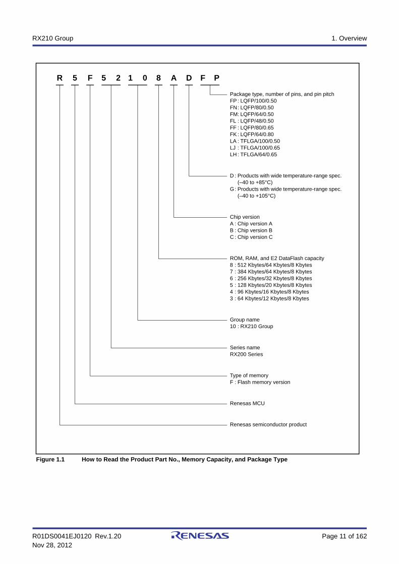
1.2 List of Products
Table 1.3 to Table 1.7 are a list of products, and Figure 1.1 shows how to read the product part no., memory capacity,
and package type.
Table 1.3 List of Products Chip Version A: D Version (Ta = 40 to +85°C)
Group Part No. PackageROM Capacity
RAM Capacity
E2 DataFlash
Operating Frequency (Max.)
Operating Temperature
RX210 R5F52108ADFP PLQP0100KB-A
512 Kbytes
64 Kbytes
8 Kbytes 50 MHz 40 to +85°C
R5F52108ADFN PLQP0080KB-A
R5F52108ADFM PLQP0064KB-A
R5F52108ADLJ PTLG0100JA-A
R5F52107ADFP PLQP0100KB-A
384 KbytesR5F52107ADFN PLQP0080KB-A
R5F52107ADFM PLQP0064KB-A
R5F52107ADLJ PTLG0100JA-A
R5F52106ADFP PLQP0100KB-A
256 Kbytes 32 KbytesR5F52106ADFN PLQP0080KB-A
R5F52106ADFM PLQP0064KB-A
R5F52106ADLJ PTLG0100JA-A
R5F52105ADFP PLQP0100KB-A
128 Kbytes 20 KbytesR5F52105ADFN PLQP0080KB-A
R5F52105ADFM PLQP0064KB-A
R5F52105ADLJ PTLG0100JA-A

R01DS0041EJ0120 Rev.1.20 Page 8 of 162Nov 28, 2012
RX210 Group 1. Overview
Note 1. Under development
Table 1.4 List of Products Chip Version B: D Version (Ta = 40 to +85°C)
Group Part No. PackageROM Capacity
RAM Capacity
E2 DataFlash
Operating Frequency (Max.)
Operating Temperature
RX210 R5F52106BDFP PLQP0100KB-A
256 Kbytes 32 Kbytes
8 Kbytes 50 MHz 40 to +85°C
R5F52106BDFN PLQP0080KB-A
R5F52106BDFM PLQP0064KB-A
R5F52106BDFL PLQP0048KB-A
R5F52106BDLJ PTLG0100JA-A
R5F52106BDLA PTLG0100KA-A
R5F52106BDFF PLQP0080JA-A *1
R5F52106BDFK PLQP0064GA-A *1
R5F52106BDLH PTLG0064JA-A *1
R5F52105BDFP PLQP0100KB-A
128 Kbytes 20 Kbytes
R5F52105BDFN PLQP0080KB-A
R5F52105BDFM PLQP0064KB-A
R5F52105BDFL PLQP0048KB-A
R5F52105BDLJ PTLG0100JA-A
R5F52105BDLA PTLG0100KA-A
R5F52105BDFF PLQP0080JA-A *1
R5F52105BDFK PLQP0064GA-A *1
R5F52105BDLH PTLG0064JA-A *1
R5F52104BDFM PLQP0064KB-A
96 Kbytes 16 KbytesR5F52104BDFL PLQP0048KB-A
R5F52104BDFF PLQP0080JA-A*1
R5F52104BDLH PTLG0064JA-A*1
R5F52103BDFM PLQP0064KB-A
64 Kbytes 12 KbytesR5F52103BDFL PLQP0048KB-A
R5F52103BDFF PLQP0080JA-A*1
R5F52103BDLH PTLG0064JA-A*1

R01DS0041EJ0120 Rev.1.20 Page 9 of 162Nov 28, 2012
RX210 Group 1. Overview
Note 1. Under development
Table 1.5 List of Products Chip Version B: G Version (Ta = 40 to +105°C)
Group Part No. PackageROM Capacity
RAM Capacity
E2 DataFlash
Operating Frequency (Max.)
Operating Temperature
RX210 R5F52106BGFP PLQP0100KB-A
256 Kbytes 32 Kbytes
8 Kbytes 50 MHz 40 to +105°C
R5F52106BGFN PLQP0080KB-A
R5F52106BGFM PLQP0064KB-A
R5F52106BGFL PLQP0048KB-A
R5F52106BGFF PLQP0080JA-A *1
R5F52106BGFK PLQP0064GA-A *1
R5F52105BGFP PLQP0100KB-A
128 Kbytes 20 Kbytes
R5F52105BGFN PLQP0080KB-A
R5F52105BGFM PLQP0064KB-A
R5F52105BGFL PLQP0048KB-A
R5F52105BGFF PLQP0080JA-A *1
R5F52105BGFK PLQP0064GA-A *1
R5F52104BGFM PLQP0064KB-A
96 Kbytes 16 KbytesR5F52104BGFL PLQP0048KB-A
R5F52104BGFF PLQP0080JA-A *1
R5F52103BGFM PLQP0064KB-A
64 Kbytes 12 KbytesR5F52103BGFL PLQP0048KB-A
R5F52103BGFF PLQP0080JA-A *1

R01DS0041EJ0120 Rev.1.20 Page 10 of 162Nov 28, 2012
RX210 Group 1. Overview
Note 1. Under development
Note 1. Under development
Table 1.6 List of Products Chip Version C: D Version (Ta = 40 to +85°C)
Group Part No. PackageROM Capacity
RAM Capacity
E2 DataFlash
Operating Frequency (Max.)
Operating Temperature
RX210 R5F52108CDFP PLQP0100KB-A
512 Kbytes
64 Kbytes 8 Kbytes 50 MHz 40 to +85°C
R5F52108CDFN PLQP0080KB-A
R5F52108CDFM PLQP0064KB-A
R5F52108CDLJ PTLG0100JA-A
R5F52108CDFF PLQP0080JA-A *1
R5F52108CDFK PLQP0064GA-A *1
R5F52107CDFP PLQP0100KB-A
384 Kbytes
R5F52107CDFN PLQP0080KB-A
R5F52107CDFM PLQP0064KB-A
R5F52107CDLJ PTLG0100JA-A
R5F52107CDFF PLQP0080JA-A *1
R5F52107CDFK PLQP0064GA-A *1
Table 1.7 List of Products Chip Version C: G Version (Ta = 40 to +105°C)
Group Part No. PackageROM Capacity
RAM Capacity
E2 DataFlash
Operating Frequency (Max.)
Operating Temperature
RX210 R5F52108CGFP PLQP0100KB-A
512 Kbytes
64 Kbytes 8 Kbytes 50 MHz 40 to +105°C
R5F52108CGFN PLQP0080KB-A
R5F52108CGFM PLQP0064KB-A
R5F52108CGFF PLQP0080JA-A *1
R5F52108CGFK PLQP0064GA-A *1
R5F52107CGFP PLQP0100KB-A
384 Kbytes
R5F52107CGFN PLQP0080KB-A
R5F52107CGFM PLQP0064KB-A
R5F52107CGFF PLQP0080JA-A *1
R5F52107CGFK PLQP0064GA-A *1
R01DS0041EJ0120 Rev.1.20 Page 11 of 162Nov 28, 2012
RX210 Group 1. Overview
Figure 1.1 How to Read the Product Part No., Memory Capacity, and Package Type
R 5 F 5 2 1 0 8 A D F P
Package type, number of pins, and pin pitchFP : LQFP/100/0.50FN: LQFP/80/0.50FM: LQFP/64/0.50FL : LQFP/48/0.50FF : LQFP/80/0.65FK : LQFP/64/0.80LA : TFLGA/100/0.50LJ : TFLGA/100/0.65LH : TFLGA/64/0.65
D : Products with wide temperature-range spec. (–40 to +85°C)
G: Products with wide temperature-range spec. (–40 to +105°C)
Chip versionA : Chip version AB : Chip version BC : Chip version C
ROM, RAM, and E2 DataFlash capacity8 : 512 Kbytes/64 Kbytes/8 Kbytes7 : 384 Kbytes/64 Kbytes/8 Kbytes6 : 256 Kbytes/32 Kbytes/8 Kbytes5 : 128 Kbytes/20 Kbytes/8 Kbytes4 : 96 Kbytes/16 Kbytes/8 Kbytes3 : 64 Kbytes/12 Kbytes/8 Kbytes
Group name10 : RX210 Group
Series nameRX200 Series
Type of memoryF : Flash memory version
Renesas MCU
Renesas semiconductor product

R01DS0041EJ0120 Rev.1.20 Page 12 of 162Nov 28, 2012
RX210 Group 1. Overview
1.3 Block Diagram
Figure 1.2 shows a block diagram.
Figure 1.2 Block Diagram
External busBSC
ICUb: Interrupt controllerDTCa: Data transfer controllerDMACA: DMA controllerBSC: Bus controllerWDTA: Watchdog timerIWDTa: Independent watchdog timerELC: Event link controllerCRC: CRC (cyclic redundancy check) calculatorSCIc, SCId: Serial communications interface
RSPI: Serial peripheral interfaceRIIC: I2C bus interfaceMTU2a: Multi-function timer pulse unit 2POE2a: Port output enable 2TMR: 8-bit timerCMT: Compare match timerRTCb: Realtime clockDOC: Data operation circuitCAC: Clock-frequency accuracy measuring circuit
Ope
rand
bus
Inst
ruct
ion
bus
Inte
rnal
mai
n b
us
1
Clock generation
circuit
RX CPU
RAM
ROM
Port 0
Port 1
Port 2
Port 3
Port 4
10-bit D/A converter × 2 channels
Temperature sensor
RIIC × 1 channel
DOC
SCIc × 6 channels
WDTA
E2 DataFlash
CRC
ELC
RTCb
MTU2a × 6 channels
12-bit A/D converter × 16 channels
CMT × 2 channels (unit 1)
CMT × 2 channels (unit 0)
TMR × 2 channels (unit 1)
TMR × 2 channels (unit 0)
RSPI × 1 channelIn
tern
al p
erip
her
al b
uses
1 to
6
Inte
rnal
ma
in b
us 2
DTCa
DMACA × 4 channels
ICUb
CAC
SCId × 1 channel
Port 5
Port A
Port B
Port C
Port D
Port E
Port H
Port J
POE2a
IWDTa
Comparator B × 2 channels
Comparator A × 2 channels
R01DS0041EJ0120 Rev.1.20 Page 13 of 162Nov 28, 2012
RX210 Group 1. Overview
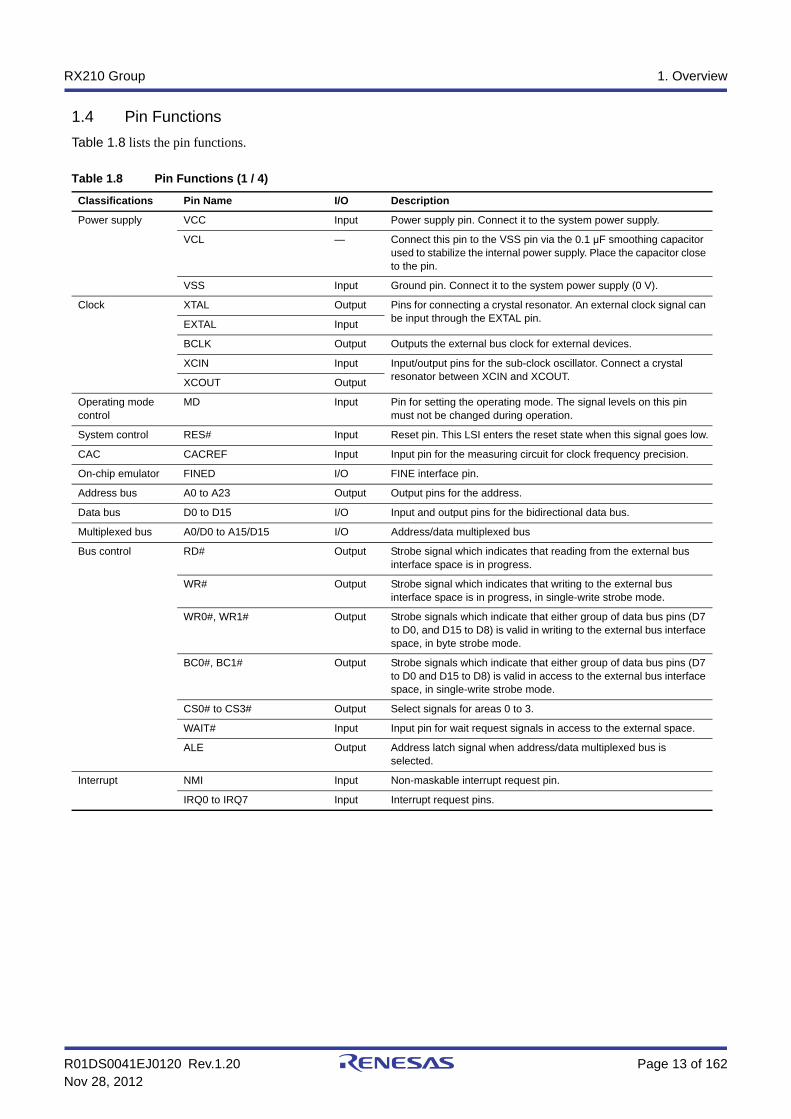
1.4 Pin Functions
Table 1.8 lists the pin functions.
Table 1.8 Pin Functions (1 / 4)
Classifications Pin Name I/O Description
Power supply VCC Input Power supply pin. Connect it to the system power supply.
VCL — Connect this pin to the VSS pin via the 0.1 μF smoothing capacitor used to stabilize the internal power supply. Place the capacitor close to the pin.
VSS Input Ground pin. Connect it to the system power supply (0 V).
Clock XTAL Output Pins for connecting a crystal resonator. An external clock signal can be input through the EXTAL pin.
EXTAL Input
BCLK Output Outputs the external bus clock for external devices.
XCIN Input Input/output pins for the sub-clock oscillator. Connect a crystal resonator between XCIN and XCOUT.
XCOUT Output
Operating mode control
MD Input Pin for setting the operating mode. The signal levels on this pin must not be changed during operation.
System control RES# Input Reset pin. This LSI enters the reset state when this signal goes low.
CAC CACREF Input Input pin for the measuring circuit for clock frequency precision.
On-chip emulator FINED I/O FINE interface pin.
Address bus A0 to A23 Output Output pins for the address.
Data bus D0 to D15 I/O Input and output pins for the bidirectional data bus.
Multiplexed bus A0/D0 to A15/D15 I/O Address/data multiplexed bus
Bus control RD# Output Strobe signal which indicates that reading from the external bus interface space is in progress.
WR# Output Strobe signal which indicates that writing to the external bus interface space is in progress, in single-write strobe mode.
WR0#, WR1# Output Strobe signals which indicate that either group of data bus pins (D7 to D0, and D15 to D8) is valid in writing to the external bus interface space, in byte strobe mode.
BC0#, BC1# Output Strobe signals which indicate that either group of data bus pins (D7 to D0 and D15 to D8) is valid in access to the external bus interface space, in single-write strobe mode.
CS0# to CS3# Output Select signals for areas 0 to 3.
WAIT# Input Input pin for wait request signals in access to the external space.
ALE Output Address latch signal when address/data multiplexed bus is selected.
Interrupt NMI Input Non-maskable interrupt request pin.
IRQ0 to IRQ7 Input Interrupt request pins.

R01DS0041EJ0120 Rev.1.20 Page 14 of 162Nov 28, 2012
RX210 Group 1. Overview
Multi-function timer pulse unit
MTIOC0A, MTIOC0BMTIOC0C, MTIOC0D
I/O The TGRA0 to TGRD0 input capture input/output compare output/PWM output pins.
MTIOC1A, MTIOC1B I/O The TGRA1 and TGRB1 input capture input/output compare output/PWM output pins.
MTIOC2A, MTIOC2B I/O The TGRA2 and TGRB2 input capture input/output compare output/PWM output pins.
MTIOC3A, MTIOC3BMTIOC3C, MTIOC3D
I/O The TGRA3 to TGRD3 input capture input/output compare output/PWM output pins.
MTIOC4A, MTIOC4BMTIOC4C, MTIOC4D
I/O The TGRA4 to TGRD4 input capture input/output compare output/PWM output pins.
MTIC5U, MTIC5V, MTIC5W Input The TGRU5, TGRV5, and TGRW5 input capture input/external pulse input pins.
MTCLKA, MTCLKB, MTCLKC, MTCLKD
Input Input pins for the external clock.
Port output enable POE0# to POE3#, POE8# Input Input pins for request signals to place the MTU pins in the high impedance state.
8-bit timer TMO0 to TMO3 Output Compare match output pins.
TMCI0 to TMCI3 Input Input pins for external clocks to be input to the counter.
TMRI0 to TMRI3 Input Input pins for the counter reset.
Realtime clock RTCOUT Output Output pin for 1-Hz clock.
RTCIC0 to RTCIC2 Input Time capture event input pins.
Serial communications interface (SCIc)
Asynchronous mode/clock synchronous mode
SCK0, SCK1, SCK5, SCK6, SCK8, SCK9
I/O Input/output pins for the clock
RXD0, RXD1, RXD5, RXD6, RXD8, RXD9
Input Input pins for received data
TXD0, TXD1, TXD5, TXD6, TXD8, TXD9
Output Output pins for transmitted data
CTS0#, CTS1#, CTS5#, CTS6#, CTS8#, CTS9#
Input Input pins for controlling the start of transmission and reception
RTS0#, RTS1#, RTS5#, RTS6#, RTS8#, RTS9#
Output Output pins for controlling the start of transmission and reception
Simple I2C mode
SSCL0, SSCL1, SSCL5, SSCL6, SSCL8, SSCL9
I/O Input/output pins for the I2C clock
SSDA0, SSDA1, SSDA5, SSDA6, SSDA8, SSDA9
I/O Input/output pins for the I2C data
Simple SPI mode
SCK0, SCK1, SCK5, SCK6, SCK8, SCK9
I/O Input/output pins for the clock
SMISO0, SMISO1, SMISO5, SMISO6, SMISO8, SMISO9
I/O Input/output pins for slave transmission of data
SMOSI0, SMOSI1, SMOSI5, SMOSI6, SMOSI8, SMOSI9
I/O Input/output pins for master transmission of data
SS0#, SS1#, SS5#, SS6#, SS8#, SS9#
Input Chip-select input pins
Table 1.8 Pin Functions (2 / 4)
Classifications Pin Name I/O Description

R01DS0041EJ0120 Rev.1.20 Page 15 of 162Nov 28, 2012
RX210 Group 1. Overview
Serial communications interface (SCId)
Asynchronous mode/clock synchronous mode
SCK12 I/O Input/output pin for the clock
RXD12 Input Input pin for received data
TXD12 Output Output pin for transmitted data
CTS12# Input Input pin for controlling the start of transmission and reception
RTS12# Output Output pin for controlling the start of transmission and reception
Simple I2C mode
SSCL12 I/O Input/output pin for the I2C clock
SSDA12 I/O Input/output pin for the I2C data
Simple SPI mode
SCK12 I/O Input/output pin for the clock
SMISO12 I/O Input/output pin for slave transmit data
SMOSI12 I/O Input/output pin for master transmit data
SS12# Input Chip-select input pin
Extended serial mode
RXDX12 Input Input pin for data reception by SCId
TXDX12 Output Output pin for data transmission by SCId
SIOX12 I/O Input/output pin for data reception or transmission by SCId
I2C bus interface SCL I/O Input/output pin for I2C bus interface clocks. Bus can be directly driven by the N-channel open-drain output.
SDA I/O Input/output pin for I2C bus interface data. Bus can be directly driven by the N-channel open-drain output.
Serial peripheral interface
RSPCKA I/O Clock input/output pin for the RSPI.
MOSIA I/O Input or output data output from the master for the RSPI.
MISOA I/O Input or output data output from the slave for the RSPI.
SSLA0 I/O Input/output pin to select the slave for the RSPI.
SSLA1 to SSLA3 Output Output pins to select the slave for the RSPI.
12-bit A/D converter AN000 to AN015 Input Input pins for the analog signals to be processed by the A/D converter.
ADTRG0# Input Input pin for the external trigger signals that start the A/D conversion.
D/A converter DA0, DA1 Output Output pins for the analog signals to be processed by the D/A converter.
Comparator A CMPA1 Input Input pin for the comparator A1 analog signal.
CMPA2 Input Input pin for the comparator A2 analog signal.
CVREFA Input Input pin for the comparator reference voltage.
Comparator B CMPB0 Input Input pin for the comparator B0 analog signal.
CVREFB0 Input Input pin for the comparator B0 reference voltage.
CMPB1 Input Input pin for the comparator B1 analog signal.
CVREFB1 Input Input pin for the comparator B1 reference voltage.
Table 1.8 Pin Functions (3 / 4)
Classifications Pin Name I/O Description

R01DS0041EJ0120 Rev.1.20 Page 16 of 162Nov 28, 2012
RX210 Group 1. Overview
Analog power supply
AVCC0 Input Analog voltage supply pin for the 12-bit A/D converter. Connect this pin to VCC if the 12-bit A/D converter is not to be used.
AVSS0 Input Analog ground pin for the 12-bit A/D converter. Connect this pin to VSS if the 12-bit A/D converter is not to be used.
VREFH0 Input Analog reference voltage supply pin for the 12-bit A/D converter. Connect this pin to VCC if the 12-bit A/D converter is not to be used.
VREFL0 Input Analog reference ground pin for the 12-bit A/D converter. Connect this pin to VSS if the 12-bit A/D converter is not to be used.
VREFH Input Analog voltage supply pin for the D/A converter. Connect this pin to VCC if the D/A converter is not to be used.
VREFL Input Analog ground pin for the D/A converter. Connect this pin to VSS if the D/A converter is not to be used.
I/O ports P03, P05, P07 I/O 3-bit input/output pins.
P12 to P17 I/O 6-bit input/output pins.
P20 to P27 I/O 8-bit input/output pins.
P30 to P37 I/O 8-bit input/output pins. (P35 input pin)
P40 to P47 I/O 8-bit input/output pins.
P50 to P55 I/O 6-bit input/output pins.
PA0 to PA7 I/O 8-bit input/output pins.
PB0 to PB7 I/O 8-bit input/output pins.
PC0 to PC7 I/O 8-bit input/output pins.
PD0 to PD7 I/O 8-bit input/output pins.
PE0 to PE7 I/O 8-bit input/output pins.
PH0 to PH3 I/O 4-bit input/output pins.
PJ1, PJ3 I/O 2-bit input/output pins.
Table 1.8 Pin Functions (4 / 4)
Classifications Pin Name I/O Description
R01DS0041EJ0120 Rev.1.20 Page 17 of 162Nov 28, 2012
RX210 Group 1. Overview
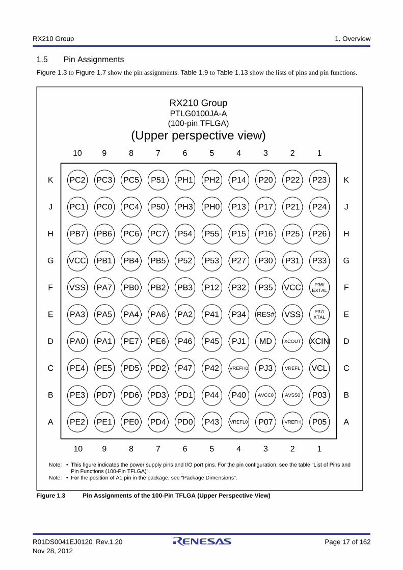
1.5 Pin Assignments
Figure 1.3 to Figure 1.7 show the pin assignments. Table 1.9 to Table 1.13 show the lists of pins and pin functions.
Figure 1.3 Pin Assignments of the 100-Pin TFLGA (Upper Perspective View)
PE2
RX210 GroupPTLG0100JA-A (100-pin TFLGA)
(Upper perspective view)
PE1 PE0 PD4 PD0 P43 VREFL0 P07 VREFH P05
PE3 PD7 PD6 PD3 PD1 P44 P40 AVCC0 AVSS0 P03
PE4 PE5 PD5 PD2 P47 P42 VREFH0 PJ3 VREFL VCL
PA0 PA1 PE7 PE6 P46 P45 PJ1 MD XCOUT XCIN
PA3 PA5 PA4 PA6 PA2 P41 P34 RES# VSS P37/XTAL
VSS PA7 PB0 PB2 PB3 P12 P32 P35 VCC P36/EXTAL
VCC PB1 PB4 PB5 P52 P53 P27 P30 P31 P33
PB7 PB6 PC6 PC7 P54 P55 P15 P16 P25 P26
P17PC1 PC0 PC4 P50 PH3 PH0 P13 P21 P24
PC2 PC3 PC5 P51 PH1 PH2 P14 P20 P22 P23 K
J
H
G
F
E
D
C
B
A
10 9 8 7 6 5 4 3 2 1
K
J
H
G
F
E
D
C
B
A
10 9 8 7 6 5 4 3 2 1
Note: • This figure indicates the power supply pins and I/O port pins. For the pin configuration, see the table “List of Pins and Pin Functions (100-Pin TFLGA)”.
Note: • For the position of A1 pin in the package, see “Package Dimensions”.

R01DS0041EJ0120 Rev.1.20 Page 18 of 162Nov 28, 2012
RX210 Group 1. Overview
Figure 1.4 Pin Assignments of the 100-Pin LQFP
1 2 3 4 5 6 7 8 9 10 11 12 13 14 15 16 17 18 19 20 21 22 23 24 25
75 74 73 72 71 70 69 68 67 66 65 64 63 62 61 60 59 58 57 56 55 54 53 52 51
50
49
48
47
46
45
44
43
42
41
40
39
38
37
36
35
34
33
32
31
30
29
28
27
26
76
77
78
79
80
81
82
83
84
85
86
87
88
89
90
91
92
93
94
95
96
97
98
99
100
PE0
PD7
PD6
PD5
PD4
PD3
PD2
PD1
PD0
P47
P46
P45
P43
P42
P41
VREFL0
P40
VREFH0
AVCC0
P07
AVSS0
PE1
P44
PC2
PC4
PC5
PC6
PC7
P50
P51
P52
P53
P54
P55
PH0
PH1
PH3
P12
P13
P14
P15
P16
P17
P20
P21
P22
PC3
PH2
PE
3
PE
5
PE
6
PE
7
PA
0
PA
1
PA
2
PA
3
PA
4
PA
5
PA
6
PA
7
VS
S
VC
C
PB
1
PB
2
PB
3
PB
4
PB
5
PB
6
PB
7
PC
0
PC
1
PE
4
PB
0
VR
EF
H
VR
EF
L
PJ3
VC
L
PJ1 MD
XC
IN
XC
OU
T
RE
S#
P37
/XT
AL
VS
S
P36
/EX
TA
L
P35
P34
P33
P32
P31
P30
P27
P26
P25
P23
P03
VC
C
PE2
P05
P24
RX210 GroupPLQP0100KB-A(100-pin LQFP)
(Top view)
Note: • This figure indicates the power supply pins and I/O port pins. For the pin configuration, see the table “List of Pins and Pin Functions (100-Pin LQFP)”.

R01DS0041EJ0120 Rev.1.20 Page 19 of 162Nov 28, 2012
RX210 Group 1. Overview
Figure 1.5 Pin Assignments of the 80-Pin LQFP
1 2 3 4 5 6 7 8 9 10 11 12 13 14 15 16 17 18 19 20
60 59 58 57 56 55 54 53 52 51 50 49 48 47 46 45 44 43 42 41
40
39
38
37
36
35
34
33
32
31
30
29
28
27
26
25
24
23
22
21
61
62
63
64
65
66
67
68
69
70
71
72
73
74
75
76
77
78
79
80
PE2
PE1
PE0
PD2
PD1
PD0
P47
P46
P45
P44
P43
P42
VREFL0
P40
VREFH0
AVCC0
P07
AVSS0
P05
P41
PC2
PC4
PC5
PC6
PC7
P54
P55
PH0
PH1
PH2
PH3
P12
P13
P15
P16
P17
P20
P21
PC3
P14
PE
3
PE
4
PE
5
PA
0
PA
1
PA
2
PA
3
PA
4
PA
5
PA
6
PB
0
VC
C
PB
1
PB
2
PB
3
PB
4
PB
5
PB
6
PB
7
VS
S
VR
EF
H
VR
EF
L
VC
L
PJ1 MD
XC
IN
XC
OU
T
RE
S#
P37
/XT
AL
VS
S
P36
/EX
TA
L
VC
C
P34
P32
P31
P30
P27
P26
P03
P35
RX210 GroupPLQP0080KB-A(80-pin LQFP)
(Top view)
Note: • This figure indicates the power supply pins and I/O port pins. For the pin configuration, see the table “List of Pins and Pin Functions (80-Pin LQFP)”.

R01DS0041EJ0120 Rev.1.20 Page 20 of 162Nov 28, 2012
RX210 Group 1. Overview
Figure 1.6 Pin Assignments of the 64-Pin LQFP
48 47 46 45 44 43 42 41 40 39 38 37 36 35 34 33
32
31
30
29
28
27
26
25
24
23
22
21
20
19
18
17
1 2 3 4 5 6 7 8 9 10
11
12
13
14
15 16
54
55
51
49
50
52
53
56
57
58
59
60
61
63
64
62
RX210 GroupPLQP0064KB-A(64-pin LQFP)
(Top view)
PE2
PE1
PE0
VREFL
P46
VREFH
P44
P43
P42
P41
VREFL0
P40
VREFH0
AVCC0
P05
AVSS0
PE
3
PE
4
PE
5
PA
0
PA
1
PA
3
PA
4
PA
6
VS
S
PB
0
VC
C
PB
1
PB
3
PB
5
PB
6
PB
7
PC2
PC3
PC4
PC5
PC6
PC7
P54
P55
PH0
PH1
PH2
PH3
P14
P15
P16
P17
P03
VC
L
MD
XC
IN
XC
OU
T
RE
S#
P37
/XT
AL
VS
S
P36
/EX
TA
L
VC
C
P35
P32
P31
P30
P27
P26
Note: • This figure indicates the power supply pins and I/O port pins. For the pin configuration, see the table “List of Pins and Pin Functions (64-Pin LQFP)”.

R01DS0041EJ0120 Rev.1.20 Page 21 of 162Nov 28, 2012
RX210 Group 1. Overview
Figure 1.7 Pin Assignments of the 48-Pin LQFP
36 35 34 33 32 31 30 29 28 27 26 25
24
23
22
21
20
19
1 2 3 4 5 6 7 8 9 10
11
12
38
39
37
40
41
42
43
44
45
47
48
46
RX210 GroupPLQP0048KB-A(48-pin LQFP)
(Top view)
PE2
PE1
VREFL
P46
VREFH
P42
P41
VREFL0
P40
VREFH0
AVCC0
AVSS0
PE
3
PE
4
PA
1
PA
3
PA
4
PA
6
VS
S
PB
0
VC
C
PB
1
PB
3
PB
5
PC4
PC5
PC6
PC7
PH0
PH1
PH2
PH3
P14
P15
P16
P17
VC
L
MD
RE
S#
P37
/XT
AL
VS
S
P36
/EX
TA
L
VC
C
P35
P31
P30
P27
P26
18
17
16
15
14
13
Note: • This figure indicates the power supply pins and I/O port pins. For the pin configuration, see the table “List of Pins and Pin Functions (48-Pin LQFP)”.

R01DS0041EJ0120 Rev.1.20 Page 22 of 162Nov 28, 2012
RX210 Group 1. Overview
Table 1.9 List of Pins and Pin Functions (100-Pin TFLGA) (1 / 3)
Pin No.
Power Supply, Clock, System Control I/O Port External Bus
Timers (MTU, TMR, POE)
Communications(SCIc, SCId, RSPI, RIIC) Others
A1 P05 DA1
A2 VREFH
A3 P07 ADTRG0#
A4 VREFL0
A5 P43 AN003
A6 PD0 D0[A0/D0] IRQ0
A7 PD4 D4[A4/D4] POE3# IRQ4
A8 PE0 D8[A8/D8] SCK12 AN008
A9 PE1 D9[A9/D9] MTIOC4C TXD12/TXDX12/SIOX12/SMOSI12/SSDA12
AN009/CMPB0
A10 PE2 D10[A10/D10] MTIOC4A RXD12/RXDX12/SMISO12/SSCL12
IRQ7-DS/AN010/CVREFB0
B1 P03 DA0
B2 AVSS0
B3 AVCC0
B4 P40 AN000
B5 P44 AN004
B6 PD1 D1[A1/D1] MTIOC4B IRQ1
B7 PD3 D3[A3/D3] POE8# IRQ3
B8 PD6 D6[A6/D6] MTIC5V/POE1# IRQ6
B9 PD7 D7[A7/D7] MTIC5U/POE0# IRQ7
B10 PE3 D11[A11/D11] MTIOC4B/POE8# CTS12#/RTS12#/SS12# AN011/CMPA1
C1 VCL
C2 VREFL
C3 PJ3 MTIOC3C CTS6#/RTS6#/SS6#
C4 VREFH0
C5 P42 AN002
C6 P47 AN007
C7 PD2 D2[A2/D2] MTIOC4D IRQ2
C8 PD5 D5[A5/D5] MTIC5W/POE2# IRQ5
C9 PE5 D13[A13/D13] MTIOC4C/MTIOC2B IRQ5/AN013
C10 PE4 D12[A12/D12] MTIOC4D/MTIOC1A AN012/CMPA2
D1 XCIN
D2 XCOUT
D3 MD FINED
D4 PJ1 MTIOC3A
D5 P45 AN005
D6 P46 AN006
D7 PE6 D14[A14/D14] IRQ6/AN014
D8 PE7 D15[A15/D15] IRQ7/AN015
D9 PA1 A1 MTIOC0B/MTCLKC SCK5/SSLA2 CVREFA
D10 PA0 A0/BC0# MTIOC4A SSLA1 CACREF
E1 XTAL P37
E2 VSS
E3 RES#
E4 P34 MTIOC0A/TMCI3/POE2#
SCK6 IRQ4
E5 P41 AN001

R01DS0041EJ0120 Rev.1.20 Page 23 of 162Nov 28, 2012
RX210 Group 1. Overview
E6 PA2 A2 RXD5/SMISO5/SSCL5/SSLA3
E7 PA6 A6 MTIC5V/MTCLKB/TMCI3/POE2#
CTS5#/RTS5#/SS5#/MOSIA
E8 PA4 A4 MTIC5U/MTCLKA/TMRI0
TXD5/SMOSI5/SSDA5/SSLA0
IRQ5-DS/CVREFB1
E9 PA5 A5 RSPCKA
E10 PA3 A3 MTIOC0D/MTCLKD RXD5/SMISO5/SSCL5 IRQ6-DS/CMPB1
F1 EXTAL P36
F2 VCC
F3 P35 NMI
F4 P32 MTIOC0C/TMO3 TXD6/SMOSI6/SSDA6 IRQ2-DS/RTCOUT/RTCIC2
F5 P12 TMCI1 SCL IRQ2
F6 PB3 A11 MTIOC0A/MTIOC4A/TMO0/POE3#
SCK6
F7 PB2 A10 CTS6#/RTS6#/SS6#
F8 PB0 A8 MTIC5W RXD6/SMISO6/SSCL6/RSPCKA
F9 PA7 A7 MISOA
F10 VSS
G1 P33 MTIOC0D/TMRI3/POE3#
RXD6/SMISO6/SSCL6 IRQ3-DS
G2 P31 MTIOC4D/TMCI2 CTS1#/RTS1#/SS1# IRQ1-DS/RTCIC1
G3 P30 MTIOC4B/TMRI3/POE8#
RXD1/SMISO1/SSCL1 IRQ0-DS/RTCIC0
G4 P27 CS3# MTIOC2B/TMCI3 SCK1
G5 BCLK P53
G6 P52 RD#
G7 PB5 A13 MTIOC2A/MTIOC1B/TMRI1/POE1#
SCK9
G8 PB4 A12 CTS9#/RTS9#/SS9#
G9 PB1 A9 MTIOC0C/MTIOC4C/TMCI0
TXD6/SMOSI6/SSDA6 IRQ4-DS
G10 VCC
H1 P26 CS2# MTIOC2A/TMO1 TXD1/SMOSI1/SSDA1
H2 P25 CS1# MTIOC4C/MTCLKB ADTRG0#
H3 P16 MTIOC3C/MTIOC3D/TMO2
TXD1/SMOSI1/SSDA1/MOSIA/SCL-DS
IRQ6/RTCOUT/ADTRG0#
H4 P15 MTIOC0B/MTCLKB/TMCI2
RXD1/SMISO1/SSCL1 IRQ5
H5 P55 WAIT# MTIOC4D/TMO3
H6 P54 ALE MTIOC4B/TMCI1
H7 PC7 A23/CS0# MTIOC3A/TMO2/MTCLKB
TXD8/SMOSI8/SSDA8/MISOA
CACREF
H8 PC6 A22/CS1# MTIOC3C/MTCLKA/TMCI2
RXD8/SMISO8/SSCL8/MOSIA
H9 PB6 A14 MTIOC3D RXD9/SMISO9/SSCL9
H10 PB7 A15 MTIOC3B TXD9/SMOSI9/SSDA9
J1 P24 CS0# MTIOC4A/MTCLKA/TMRI1
J2 P21 MTIOC1B/TMCI0 RXD0/SMISO0/SSCL0
J3 P17 MTIOC3A/MTIOC3B/TMO1/POE8#
SCK1/MISOA/SDA-DS
IRQ7
Table 1.9 List of Pins and Pin Functions (100-Pin TFLGA) (2 / 3)
Pin No.
Power Supply, Clock, System Control I/O Port External Bus
Timers (MTU, TMR, POE)
Communications(SCIc, SCId, RSPI, RIIC) Others

R01DS0041EJ0120 Rev.1.20 Page 24 of 162Nov 28, 2012
RX210 Group 1. Overview
Note: • Pin names to which –DS is appended are for pins that can be used to trigger release from deep software standby mode.
J4 P13 MTIOC0B/TMO3 SDA IRQ3
J5 PH0 CACREF
J6 PH3 TMCI0
J7 P50 WR0#/WR#
J8 PC4 A20/CS3# MTIOC3D/MTCLKC/TMCI1/POE0#
SCK5/CTS8#/RTS8#/SS8#/SSLA0
J9 PC0 A16 MTIOC3C CTS5#/RTS5#/SS5#/SSLA1
J10 PC1 A17 MTIOC3A SCK5/SSLA2
K1 P23 MTIOC3D/MTCLKD CTS0#/RTS0#/SS0#
K2 P22 MTIOC3B/MTCLKC/TMO0
SCK0
K3 P20 MTIOC1A/TMRI0 TXD0/SMOSI0/SSDA0
K4 P14 MTIOC3A/MTCLKA/TMRI2
CTS1#/RTS1#/SS1# IRQ4
K5 PH2 TMRI0 IRQ1
K6 PH1 TMO0 IRQ0
K7 P51 WR1#/BC1#/WAIT#
K8 PC5 A21/CS2#/WAIT# MTIOC3B/MTCLKD/TMRI2
SCK8/RSPCKA
K9 PC3 A19 MTIOC4D TXD5/SMOSI5/SSDA5
K10 PC2 A18 MTIOC4B RXD5/SMISO5/SSCL5
Table 1.9 List of Pins and Pin Functions (100-Pin TFLGA) (3 / 3)
Pin No.
Power Supply, Clock, System Control I/O Port External Bus
Timers (MTU, TMR, POE)
Communications(SCIc, SCId, RSPI, RIIC) Others

R01DS0041EJ0120 Rev.1.20 Page 25 of 162Nov 28, 2012
RX210 Group 1. Overview
Table 1.10 List of Pins and Pin Functions (100-Pin LQFP) (1 / 3)
Pin No.
Power Supply, Clock, System Control I/O Port External Bus
Timers (MTU, TMR, POE)
Communications(SCIc, SCId, RSPI, RIIC) Others
1 VREFH
2 P03 DA0
3 VREFL
4 PJ3 MTIOC3C CTS6#/RTS6#/SS6#
5 VCL
6 PJ1 MTIOC3A
7 MD FINED
8 XCIN
9 XCOUT
10 RES#
11 XTAL P37
12 VSS
13 EXTAL P36
14 VCC
15 P35 NMI
16 P34 MTIOC0A/TMCI3/POE2#
SCK6 IRQ4
17 P33 MTIOC0D/TMRI3/POE3#
RXD6/SMISO6/SSCL6 IRQ3-DS
18 P32 MTIOC0C/TMO3 TXD6/SMOSI6/SSDA6 IRQ2-DS/RTCOUT/RTCIC2
19 P31 MTIOC4D/TMCI2 CTS1#/RTS1#/SS1# IRQ1-DS/RTCIC1
20 P30 MTIOC4B/TMRI3/POE8#
RXD1/SMISO1/SSCL1 IRQ0-DS/RTCIC0
21 P27 CS3# MTIOC2B/TMCI3 SCK1
22 P26 CS2# MTIOC2A/TMO1 TXD1/SMOSI1/SSDA1
23 P25 CS1# MTIOC4C/MTCLKB ADTRG0#
24 P24 CS0# MTIOC4A/MTCLKA/TMRI1
25 P23 MTIOC3D/MTCLKD CTS0#/RTS0#/SS0#
26 P22 MTIOC3B/MTCLKC/TMO0
SCK0
27 P21 MTIOC1B/TMCI0 RXD0/SMISO0/SSCL0
28 P20 MTIOC1A/TMRI0 TXD0/SMOSI0/SSDA0
29 P17 MTIOC3A/MTIOC3B/TMO1/POE8#
SCK1/MISOA/SDA-DS
IRQ7
30 P16 MTIOC3C/MTIOC3D/TMO2
TXD1/SMOSI1/SSDA1/MOSIA/SCL-DS
IRQ6/RTCOUT/ADTRG0#
31 P15 MTIOC0B/MTCLKB/TMCI2
RXD1/SMISO1/SSCL1 IRQ5
32 P14 MTIOC3A/MTCLKA/TMRI2
CTS1#/RTS1#/SS1# IRQ4
33 P13 MTIOC0B/TMO3 SDA IRQ3
34 P12 TMCI1 SCL IRQ2
35 PH3 TMCI0
36 PH2 TMRI0 IRQ1
37 PH1 TMO0 IRQ0
38 PH0 CACREF
39 P55 WAIT# MTIOC4D/TMO3
40 P54 ALE MTIOC4B/TMCI1
41 BCLK P53

R01DS0041EJ0120 Rev.1.20 Page 26 of 162Nov 28, 2012
RX210 Group 1. Overview
42 P52 RD#
43 P51 WR1#/BC1#/WAIT#
44 P50 WR0#/WR#
45 PC7 A23/CS0# MTIOC3A/TMO2/MTCLKB
TXD8/SMOSI8/SSDA8/MISOA
CACREF
46 PC6 A22/CS1# MTIOC3C/MTCLKA/TMCI2
RXD8/SMISO8/SSCL8/MOSIA
47 PC5 A21/CS2#/WAIT# MTIOC3B/MTCLKD/TMRI2
SCK8/RSPCKA
48 PC4 A20/CS3# MTIOC3D/MTCLKC/TMCI1/POE0#
SCK5/CTS8#/RTS8#/SS8#/SSLA0
49 PC3 A19 MTIOC4D TXD5/SMOSI5/SSDA5
50 PC2 A18 MTIOC4B RXD5/SMISO5/SSCL5/SSLA3
51 PC1 A17 MTIOC3A SCK5/SSLA2
52 PC0 A16 MTIOC3C CTS5#/RTS5#/SS5#/SSLA1
53 PB7 A15 MTIOC3B TXD9/SMOSI9/SSDA9
54 PB6 A14 MTIOC3D RXD9/SMISO9/SSCL9
55 PB5 A13 MTIOC2A/MTIOC1B/TMRI1/POE1#
SCK9
56 PB4 A12 CTS9#/RTS9#/SS9#
57 PB3 A11 MTIOC0A/MTIOC4A/TMO0/POE3#
SCK6
58 PB2 A10 CTS6#/RTS6#/SS6#
59 PB1 A9 MTIOC0C/MTIOC4C/TMCI0
TXD6/SMOSI6/SSDA6 IRQ4-DS
60 VCC
61 PB0 A8 MTIC5W RXD6/SMISO6/SSCL6/RSPCKA
62 VSS
63 PA7 A7 MISOA
64 PA6 A6 MTIC5V/MTCLKB/TMCI3/POE2#
CTS5#/RTS5#/SS5#/MOSIA
65 PA5 A5 RSPCKA
66 PA4 A4 MTIC5U/MTCLKA/TMRI0
TXD5/SMOSI5/SSDA5/SSLA0
IRQ5-DS/CVREFB1
67 PA3 A3 MTIOC0D/MTCLKD RXD5/SMISO5/SSCL5 IRQ6-DS/CMPB1
68 PA2 A2 RXD5/SMISO5/SSCL5/SSLA3
69 PA1 A1 MTIOC0B/MTCLKC SCK5/SSLA2 CVREFA
70 PA0 A0/BC0# MTIOC4A SSLA1 CACREF
71 PE7 D15[A15/D15] IRQ7/AN015
72 PE6 D14[A14/D14] IRQ6/AN014
73 PE5 D13[A13/D13] MTIOC4C/MTIOC2B IRQ5/AN013
74 PE4 D12[A12/D12] MTIOC4D/MTIOC1A AN012/CMPA2
75 PE3 D11[A11/D11] MTIOC4B/POE8# CTS12#/RTS12#/SS12# AN011/CMPA1
76 PE2 D10[A10/D10] MTIOC4A RXD12/RXDX12/SMISO12/SSCL12
IRQ7-DS/AN010/CVREFB0
77 PE1 D9[A9/D9] MTIOC4C TXD12/TXDX12/SIOX12/SMOSI12/SSDA12
AN009/CMPB0
78 PE0 D8[A8/D8] SCK12 AN008
79 PD7 D7[A7/D7] MTIC5U/POE0# IRQ7
Table 1.10 List of Pins and Pin Functions (100-Pin LQFP) (2 / 3)
Pin No.
Power Supply, Clock, System Control I/O Port External Bus
Timers (MTU, TMR, POE)
Communications(SCIc, SCId, RSPI, RIIC) Others

R01DS0041EJ0120 Rev.1.20 Page 27 of 162Nov 28, 2012
RX210 Group 1. Overview
Note: • Pin names to which –DS is appended are for pins that can be used to trigger release from deep software standby mode.
80 PD6 D6[A6/D6] MTIC5V/POE1# IRQ6
81 PD5 D5[A5/D5] MTIC5W/POE2# IRQ5
82 PD4 D4[A4/D4] POE3# IRQ4
83 PD3 D3[A3/D3] POE8# IRQ3
84 PD2 D2[A2/D2] MTIOC4D IRQ2
85 PD1 D1[A1/D1] MTIOC4B IRQ1
86 PD0 D0[A0/D0] IRQ0
87 P47 AN007
88 P46 AN006
89 P45 AN005
90 P44 AN004
91 P43 AN003
92 P42 AN002
93 P41 AN001
94 VREFL0
95 P40 AN000
96 VREFH0
97 AVCC0
98 P07 ADTRG0#
99 AVSS0
100 P05 DA1
Table 1.10 List of Pins and Pin Functions (100-Pin LQFP) (3 / 3)
Pin No.
Power Supply, Clock, System Control I/O Port External Bus
Timers (MTU, TMR, POE)
Communications(SCIc, SCId, RSPI, RIIC) Others
R01DS0041EJ0120 Rev.1.20 Page 28 of 162Nov 28, 2012
RX210 Group 1. Overview
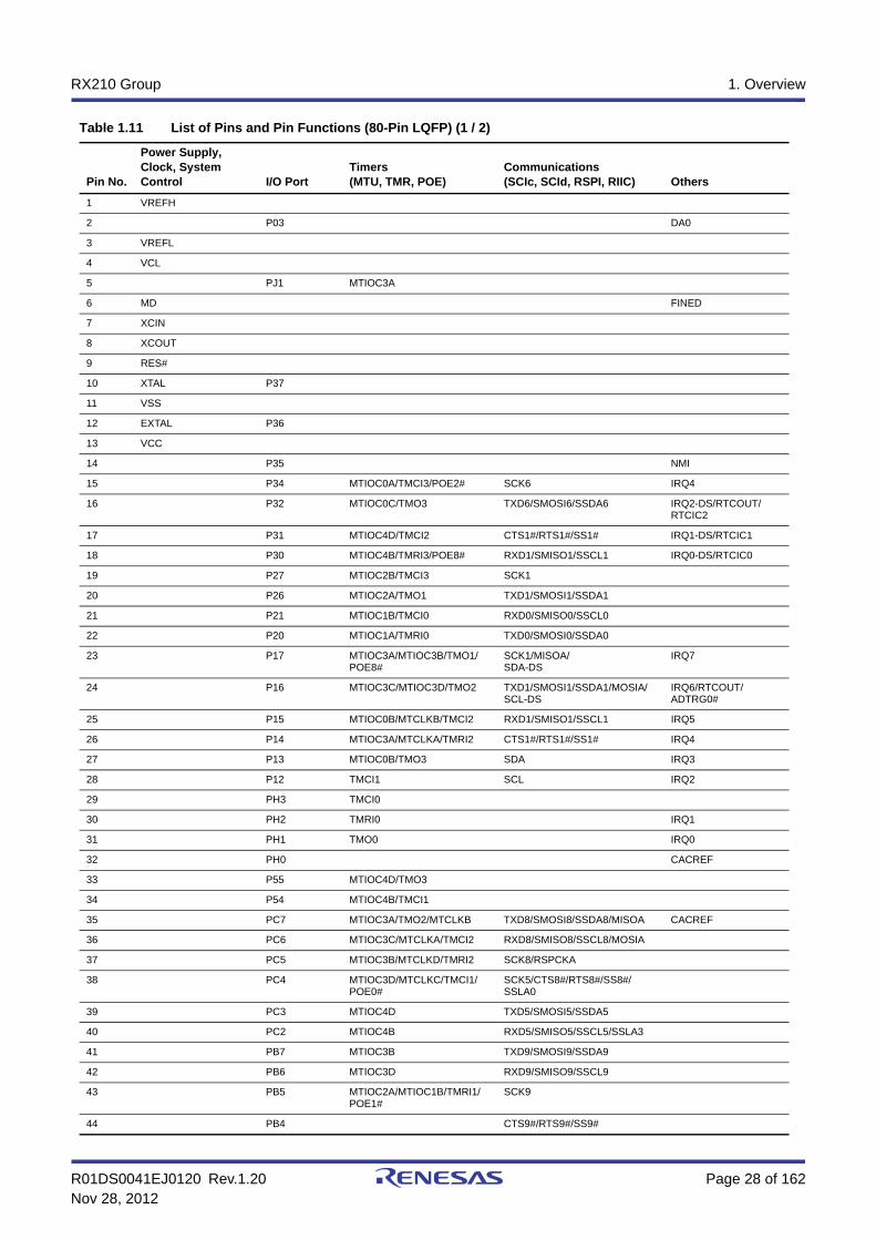
Table 1.11 List of Pins and Pin Functions (80-Pin LQFP) (1 / 2)
Pin No.
Power Supply, Clock, System Control I/O Port
Timers(MTU, TMR, POE)
Communications (SCIc, SCId, RSPI, RIIC) Others
1 VREFH
2 P03 DA0
3 VREFL
4 VCL
5 PJ1 MTIOC3A
6 MD FINED
7 XCIN
8 XCOUT
9 RES#
10 XTAL P37
11 VSS
12 EXTAL P36
13 VCC
14 P35 NMI
15 P34 MTIOC0A/TMCI3/POE2# SCK6 IRQ4
16 P32 MTIOC0C/TMO3 TXD6/SMOSI6/SSDA6 IRQ2-DS/RTCOUT/RTCIC2
17 P31 MTIOC4D/TMCI2 CTS1#/RTS1#/SS1# IRQ1-DS/RTCIC1
18 P30 MTIOC4B/TMRI3/POE8# RXD1/SMISO1/SSCL1 IRQ0-DS/RTCIC0
19 P27 MTIOC2B/TMCI3 SCK1
20 P26 MTIOC2A/TMO1 TXD1/SMOSI1/SSDA1
21 P21 MTIOC1B/TMCI0 RXD0/SMISO0/SSCL0
22 P20 MTIOC1A/TMRI0 TXD0/SMOSI0/SSDA0
23 P17 MTIOC3A/MTIOC3B/TMO1/POE8#
SCK1/MISOA/SDA-DS
IRQ7
24 P16 MTIOC3C/MTIOC3D/TMO2 TXD1/SMOSI1/SSDA1/MOSIA/SCL-DS
IRQ6/RTCOUT/ADTRG0#
25 P15 MTIOC0B/MTCLKB/TMCI2 RXD1/SMISO1/SSCL1 IRQ5
26 P14 MTIOC3A/MTCLKA/TMRI2 CTS1#/RTS1#/SS1# IRQ4
27 P13 MTIOC0B/TMO3 SDA IRQ3
28 P12 TMCI1 SCL IRQ2
29 PH3 TMCI0
30 PH2 TMRI0 IRQ1
31 PH1 TMO0 IRQ0
32 PH0 CACREF
33 P55 MTIOC4D/TMO3
34 P54 MTIOC4B/TMCI1
35 PC7 MTIOC3A/TMO2/MTCLKB TXD8/SMOSI8/SSDA8/MISOA CACREF
36 PC6 MTIOC3C/MTCLKA/TMCI2 RXD8/SMISO8/SSCL8/MOSIA
37 PC5 MTIOC3B/MTCLKD/TMRI2 SCK8/RSPCKA
38 PC4 MTIOC3D/MTCLKC/TMCI1/POE0#
SCK5/CTS8#/RTS8#/SS8#/SSLA0
39 PC3 MTIOC4D TXD5/SMOSI5/SSDA5
40 PC2 MTIOC4B RXD5/SMISO5/SSCL5/SSLA3
41 PB7 MTIOC3B TXD9/SMOSI9/SSDA9
42 PB6 MTIOC3D RXD9/SMISO9/SSCL9
43 PB5 MTIOC2A/MTIOC1B/TMRI1/POE1#
SCK9
44 PB4 CTS9#/RTS9#/SS9#

R01DS0041EJ0120 Rev.1.20 Page 29 of 162Nov 28, 2012
RX210 Group 1. Overview
Note: • Pin names to which –DS is appended are for pins that can be used to trigger release from deep software standby mode.
45 PB3 MTIOC0A/MTIOC4A/TMO0/POE3#
SCK6
46 PB2 CTS6#/RTS6#/SS6#
47 PB1 MTIOC0C/MTIOC4C/TMCI0 TXD6/SMOSI6/SSDA6 IRQ4-DS
48 VCC
49 PB0 MTIC5W RXD6/SMISO6/SSCL6/RSPCKA
50 VSS
51 PA6 MTIC5V/MTCLKB/TMCI3/POE2#
CTS5#/RTS5#/SS5#/MOSIA
52 PA5 RSPCKA
53 PA4 MTIC5U/MTCLKA/TMRI0 TXD5/SMOSI5/SSDA5/SSLA0 IRQ5-DS/CVREFB1
54 PA3 MTIOC0D/MTCLKD RXD5/SMISO5/SSCL5 IRQ6-DS/CMPB1
55 PA2 RXD5/SMISO5/SSCL5/SSLA3
56 PA1 MTIOC0B/MTCLKC SCK5/SSLA2 CVREFA
57 PA0 MTIOC4A SSLA1 CACREF
58 PE5 MTIOC4C/MTIOC2B IRQ5/AN013
59 PE4 MTIOC4D/MTIOC1A AN012/CMPA2
60 PE3 MTIOC4B/POE8# CTS12#/RTS12#/SS12# AN011/CMPA1
61 PE2 MTIOC4A RXD12/RXDX12/SMISO12/SSCL12
IRQ7-DS/AN010/CVREFB0
62 PE1 MTIOC4C TXD12/TXDX12/SIOX12/SMOSI12/SSDA12
AN009/CMPB0
63 PE0 SCK12 AN008
64 PD2 MTIOC4D IRQ2
65 PD1 MTIOC4B IRQ1
66 PD0 IRQ0
67 P47 AN007
68 P46 AN006
69 P45 AN005
70 P44 AN004
71 P43 AN003
72 P42 AN002
73 P41 AN001
74 VREFL0
75 P40 AN000
76 VREFH0
77 AVCC0
78 P07 ADTRG0#
79 AVSS0
80 P05 DA1
Table 1.11 List of Pins and Pin Functions (80-Pin LQFP) (2 / 2)
Pin No.
Power Supply, Clock, System Control I/O Port
Timers(MTU, TMR, POE)
Communications (SCIc, SCId, RSPI, RIIC) Others

R01DS0041EJ0120 Rev.1.20 Page 30 of 162Nov 28, 2012
RX210 Group 1. Overview
Table 1.12 List of Pins and Pin Functions (64-Pin LQFP) (1 / 2)
Pin No.
Power Supply, Clock, System Control I/O Port
Timers(MTU, TMR, POE)
Communication (SCIc, SCId, RSPI, RIIC) Others
1 P03 DA0
2 VCL
3 MD FINED
4 XCIN
5 XCOUT
6 RES#
7 XTAL P37
8 VSS
9 EXTAL P36
10 VCC
11 P35 NMI
12 P32 MTIOC0C/TMO3 TXD6/SMOSI6/SSDA6 IRQ2-DS/RTCOUT/RTCIC2
13 P31 MTIOC4D/TMCI2 CTS1#/RTS1#/SS1# IRQ1-DS/RTCIC1
14 P30 MTIOC4B/TMRI3/POE8# RXD1/SMISO1/SSCL1 IRQ0-DS/RTCIC0
15 P27 MTIOC2B/TMCI3 SCK1
16 P26 MTIOC2A/TMO1 TXD1/SMOSI1/SSDA1
17 P17 MTIOC3A/MTIOC3B/TMO1/POE8#
SCK1/MISOA/SDA-DS IRQ7
18 P16 MTIOC3C/MTIOC3D/TMO2 TXD1/SMOSI1/SSDA1/MOSIA/SCL-DS
IRQ6/RTCOUT/ADTRG0#
19 P15 MTIOC0B/MTCLKB/TMCI2 RXD1/SMISO1/SSCL1 IRQ5
20 P14 MTIOC3A/MTCLKA/TMRI2 CTS1#/RTS1#/SS1# IRQ4
21 PH3 TMCI0
22 PH2 TMRI0 IRQ1
23 PH1 TMO0 IRQ0
24 PH0 CACREF
25 P55 MTIOC4D/TMO3
26 P54 MTIOC4B/TMCI1
27 PC7 MTIOC3A/TMO2/MTCLKB TXD8/SMOSI8/SSDA8/MISOA CACREF
28 PC6 MTIOC3C/MTCLKA/TMCI2 RXD8/SMISO8/SSCL8/MOSIA
29 PC5 MTIOC3B/MTCLKD/TMRI2 SCK8/RSPCKA
30 PC4 MTIOC3D/MTCLKC/TMCI1/POE0#
SCK5/CTS8#/RTS8#/SS8#/SSLA0
31 PC3 MTIOC4D TXD5/SMOSI5/SSDA5
32 PC2 MTIOC4B RXD5/SMISO5/SSCL5/SSLA3
33 PB7 MTIOC3B TXD9/SMOSI9/SSDA9
34 PB6 MTIOC3D RXD9/SMISO9/SSCL9
35 PB5 MTIOC2A/MTIOC1B/TMRI1/POE1#
SCK9
36 PB3 MTIOC0A/MTIOC4A/TMO0/POE3#
SCK6
37 PB1 MTIOC0C/MTIOC4C/TMCI0 TXD6/SMOSI6/SSDA6 IRQ4-DS
38 VCC
39 PB0 MTIC5W RXD6/SMISO6/SSCL6/RSPCKA
40 VSS
41 PA6 MTIC5V/MTCLKB/TMCI3/POE2#
CTS5#/RTS5#/SS5#/MOSIA
42 PA4 MTIC5U/MTCLKA/TMRI0 TXD5/SMOSI5/SSDA5/SSLA0 IRQ5-DS/CVREFB1
43 PA3 MTIOC0D/MTCLKD RXD5/SMISO5/SSCL5 IRQ6-DS/CMPB1

R01DS0041EJ0120 Rev.1.20 Page 31 of 162Nov 28, 2012
RX210 Group 1. Overview
Note: • Pin names to which –DS is appended are for pins that can be used to trigger release from deep software standby mode.
44 PA1 MTIOC0B/MTCLKC SCK5/SSLA2 CVREFA
45 PA0 MTIOC4A SSLA1 CACREF
46 PE5 MTIOC4C/MTIOC2B IRQ5/AN013
47 PE4 MTIOC4D/MTIOC1A AN012/CMPA2
48 PE3 MTIOC4B/POE8# CTS12#/RTS12#/SS12# AN011/CMPA1
49 PE2 MTIOC4A RXD12/RXDX12/SMISO12/SSCL12
IRQ7-DS/AN010/CVREFB0
50 PE1 MTIOC4C TXD12/TXDX12/SIOX12/SMOSI12/SSDA12
AN009/CMPB0
51 PE0 SCK12 AN008
52 VREFL
53 P46 AN006
54 VREFH
55 P44 AN004
56 P43 AN003
57 P42 AN002
58 P41 AN001
59 VREFL0
60 P40 AN000
61 VREFH0
62 AVCC0
63 P05 DA1
64 AVSS0
Table 1.12 List of Pins and Pin Functions (64-Pin LQFP) (2 / 2)
Pin No.
Power Supply, Clock, System Control I/O Port
Timers(MTU, TMR, POE)
Communication (SCIc, SCId, RSPI, RIIC) Others
R01DS0041EJ0120 Rev.1.20 Page 32 of 162Nov 28, 2012
RX210 Group 1. Overview
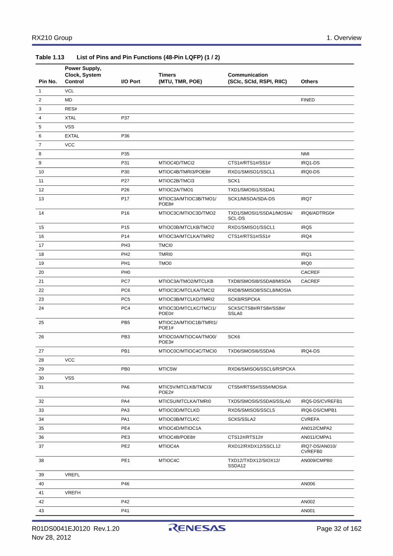
Table 1.13 List of Pins and Pin Functions (48-Pin LQFP) (1 / 2)
Pin No.
Power Supply, Clock, System Control I/O Port
Timers(MTU, TMR, POE)
Communication (SCIc, SCId, RSPI, RIIC) Others
1 VCL
2 MD FINED
3 RES#
4 XTAL P37
5 VSS
6 EXTAL P36
7 VCC
8 P35 NMI
9 P31 MTIOC4D/TMCI2 CTS1#/RTS1#/SS1# IRQ1-DS
10 P30 MTIOC4B/TMRI3/POE8# RXD1/SMISO1/SSCL1 IRQ0-DS
11 P27 MTIOC2B/TMCI3 SCK1
12 P26 MTIOC2A/TMO1 TXD1/SMOSI1/SSDA1
13 P17 MTIOC3A/MTIOC3B/TMO1/POE8#
SCK1/MISOA/SDA-DS IRQ7
14 P16 MTIOC3C/MTIOC3D/TMO2 TXD1/SMOSI1/SSDA1/MOSIA/SCL-DS
IRQ6/ADTRG0#
15 P15 MTIOC0B/MTCLKB/TMCI2 RXD1/SMISO1/SSCL1 IRQ5
16 P14 MTIOC3A/MTCLKA/TMRI2 CTS1#/RTS1#/SS1# IRQ4
17 PH3 TMCI0
18 PH2 TMRI0 IRQ1
19 PH1 TMO0 IRQ0
20 PH0 CACREF
21 PC7 MTIOC3A/TMO2/MTCLKB TXD8/SMOSI8/SSDA8/MISOA CACREF
22 PC6 MTIOC3C/MTCLKA/TMCI2 RXD8/SMISO8/SSCL8/MOSIA
23 PC5 MTIOC3B/MTCLKD/TMRI2 SCK8/RSPCKA
24 PC4 MTIOC3D/MTCLKC/TMCI1/POE0#
SCK5/CTS8#/RTS8#/SS8#/SSLA0
25 PB5 MTIOC2A/MTIOC1B/TMRI1/POE1#
26 PB3 MTIOC0A/MTIOC4A/TMO0/POE3#
SCK6
27 PB1 MTIOC0C/MTIOC4C/TMCI0 TXD6/SMOSI6/SSDA6 IRQ4-DS
28 VCC
29 PB0 MTIC5W RXD6/SMISO6/SSCL6/RSPCKA
30 VSS
31 PA6 MTIC5V/MTCLKB/TMCI3/POE2#
CTS5#/RTS5#/SS5#/MOSIA
32 PA4 MTIC5U/MTCLKA/TMRI0 TXD5/SMOSI5/SSDA5/SSLA0 IRQ5-DS/CVREFB1
33 PA3 MTIOC0D/MTCLKD RXD5/SMISO5/SSCL5 IRQ6-DS/CMPB1
34 PA1 MTIOC0B/MTCLKC SCK5/SSLA2 CVREFA
35 PE4 MTIOC4D/MTIOC1A AN012/CMPA2
36 PE3 MTIOC4B/POE8# CTS12#/RTS12# AN011/CMPA1
37 PE2 MTIOC4A RXD12/RXDX12/SSCL12 IRQ7-DS/AN010/CVREFB0
38 PE1 MTIOC4C TXD12/TXDX12/SIOX12/SSDA12
AN009/CMPB0
39 VREFL
40 P46 AN006
41 VREFH
42 P42 AN002
43 P41 AN001
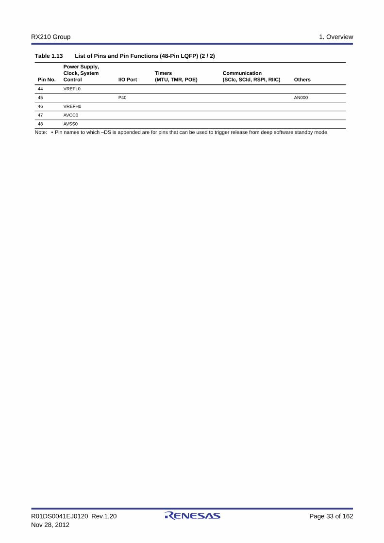
R01DS0041EJ0120 Rev.1.20 Page 33 of 162Nov 28, 2012
RX210 Group 1. Overview
Note: • Pin names to which –DS is appended are for pins that can be used to trigger release from deep software standby mode.
44 VREFL0
45 P40 AN000
46 VREFH0
47 AVCC0
48 AVSS0
Table 1.13 List of Pins and Pin Functions (48-Pin LQFP) (2 / 2)
Pin No.
Power Supply, Clock, System Control I/O Port
Timers(MTU, TMR, POE)
Communication (SCIc, SCId, RSPI, RIIC) Others

R01DS0041EJ0120 Rev.1.20 Page 34 of 162Nov 28, 2012
RX210 Group 2. CPU
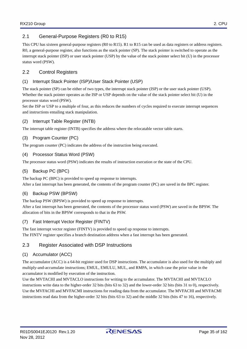
2. CPUFigure 2.1 shows the register set of the CPU.
Figure 2.1 Register Set of the CPU
Note 1. The stack pointer (SP) can be the interrupt stack pointer (ISP) or user stack pointer (USP), according to the value of the U bit in the PSW register.
USP (User stack pointer)
ISP (Interrupt stack pointer)
INTB (Interrupt table register)
PC (Program counter)
PSW (Processor status word)
BPC (Backup PC)
BPSW (Backup PSW)
FINTV (Fast interrupt vector register)
R15
R14
R13
R12
R11
R10
R9
R8
R7
R6
R5
R4
R3
R2
R1
R0 (SP) *1
General-purpose register
Control register
b31 b0
b31 b0
DSP instruction register
b63 b0
ACC (Accumulator)
R01DS0041EJ0120 Rev.1.20 Page 35 of 162Nov 28, 2012
RX210 Group 2. CPU
2.1 General-Purpose Registers (R0 to R15)
This CPU has sixteen general-purpose registers (R0 to R15). R1 to R15 can be used as data registers or address registers.
R0, a general-purpose register, also functions as the stack pointer (SP). The stack pointer is switched to operate as the
interrupt stack pointer (ISP) or user stack pointer (USP) by the value of the stack pointer select bit (U) in the processor
status word (PSW).
2.2 Control Registers
(1) Interrupt Stack Pointer (ISP)/User Stack Pointer (USP)
The stack pointer (SP) can be either of two types, the interrupt stack pointer (ISP) or the user stack pointer (USP).
Whether the stack pointer operates as the ISP or USP depends on the value of the stack pointer select bit (U) in the
processor status word (PSW).
Set the ISP or USP to a multiple of four, as this reduces the numbers of cycles required to execute interrupt sequences
and instructions entailing stack manipulation.
(2) Interrupt Table Register (INTB)
The interrupt table register (INTB) specifies the address where the relocatable vector table starts.
(3) Program Counter (PC)
The program counter (PC) indicates the address of the instruction being executed.
(4) Processor Status Word (PSW)
The processor status word (PSW) indicates the results of instruction execution or the state of the CPU.
(5) Backup PC (BPC)
The backup PC (BPC) is provided to speed up response to interrupts.
After a fast interrupt has been generated, the contents of the program counter (PC) are saved in the BPC register.
(6) Backup PSW (BPSW)
The backup PSW (BPSW) is provided to speed up response to interrupts.
After a fast interrupt has been generated, the contents of the processor status word (PSW) are saved in the BPSW. The
allocation of bits in the BPSW corresponds to that in the PSW.
(7) Fast Interrupt Vector Register (FINTV)
The fast interrupt vector register (FINTV) is provided to speed up response to interrupts.
The FINTV register specifies a branch destination address when a fast interrupt has been generated.
2.3 Register Associated with DSP Instructions
(1) Accumulator (ACC)
The accumulator (ACC) is a 64-bit register used for DSP instructions. The accumulator is also used for the multiply and
multiply-and-accumulate instructions; EMUL, EMULU, MUL, and RMPA, in which case the prior value in the
accumulator is modified by execution of the instruction.
Use the MVTACHI and MVTACLO instructions for writing to the accumulator. The MVTACHI and MVTACLO
instructions write data to the higher-order 32 bits (bits 63 to 32) and the lower-order 32 bits (bits 31 to 0), respectively.
Use the MVFACHI and MVFACMI instructions for reading data from the accumulator. The MVFACHI and MVFACMI
instructions read data from the higher-order 32 bits (bits 63 to 32) and the middle 32 bits (bits 47 to 16), respectively.
R01DS0041EJ0120 Rev.1.20 Page 36 of 162Nov 28, 2012
RX210 Group 3. Address Space
3. Address Space
3.1 Address Space
This LSI has a 4-Gbyte address space, consisting of the range of addresses from 0000 0000h to FFFF FFFFh. That is,
linear access to an address space of up to 4 Gbytes is possible, and this contains both program and data areas.
Figure 3.1 shows the memory maps in the respective operating modes. Accessible areas will differ according to the
operating mode and states of control bits.
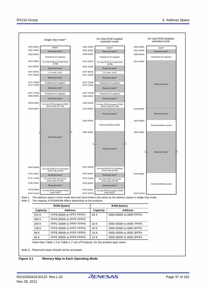
R01DS0041EJ0120 Rev.1.20 Page 37 of 162Nov 28, 2012
RX210 Group 3. Address Space
Figure 3.1 Memory Map in Each Operating Mode
Reserved area*3
Reserved area*3
Reserved area*3
Reserved area*3
Reserved area*3
Reserved area*3
Reserved area*3
On-chip ROM (E2 DataFlash) (8 KB)
Reserved area*3
0000 0000h
0008 0000h
FFFF FFFFh
Single-chip mode*1
RAM*2
On-chip ROM (program ROM)(read only)*2
0010 0000h
Peripheral I/O registers
0010 2000h
0080 0000h
0100 0000h
On-chip ROM (program ROM)(write only) (512 KB)
FFF8 0000h
FF7F C000h On-chip ROM (user boot) (read only) (16 KB)
FCU-RAM (8 KB)
Peripheral I/O registers
Peripheral I/O registers
007F 8000h
007F A000h
007F C000h007F C500h
007F FC00h
0001 0000h
FF80 0000h
00F8 0000h
On-chip ROM (FCU firmware)(read only) (8 KB)
FEFF E000h
FF00 0000h
Reserved area*3
Reserved area*3
Reserved area*3
Reserved area*3
Reserved area*3
Reserved area*3
Reserved area*3
Reserved area*3
Reserved area*3
0000 0000h
0008 0000h
FFFF FFFFh
On-chip ROM enabled extended mode
RAM*2
On-chip ROM (program ROM)(read only)*2
0010 0000h
Peripheral I/O registers
0010 2000h
On-chip ROM (E2 DataFlash) (8 KB)
0080 0000h
0100 0000h
On-chip ROM (program ROM)(write only) (512 KB)
0800 0000h
FFF8 0000h
FF7F C000h On-chip ROM (user boot) (read only) (16 KB)
FCU-RAM (8 KB)
Peripheral I/O registers
Peripheral I/O registers
007F 8000h
007F A000h
007F C000h007F C500h
007F FC00h
0001 0000h
External address space
FF80 0000h
00F8 0000h
On-chip ROM (FCU firmware)(read only) (8 KB)
FEFF E000h
FF00 0000h
0500 0000h
Reserved area*3
Reserved area*3
Reserved area*3
Reserved area*3
0000 0000h
0008 0000h
FFFF FFFFh
On-chip ROM disabled extended mode
RAM*2
0010 0000h
Peripheral I/O registers
0100 0000h
0800 0000h
FF00 0000h
0001 0000h
External address space
External address space
0500 0000h
Note 1. The address space in boot mode and user boot mode is the same as the address space in single-chip mode.Note 2. The capacity of ROM/RAM differs depending on the products.
Note:•See Table 1.3 to Table 1.7 List of Products, for the product type name.
Note 3. Reserved areas should not be accessed.
ROM (bytes) RAM (bytes)
Capacity Address Capacity Address
512 K FFF8 0000h to FFFF FFFFh 64 K 0000 0000h to 0000 FFFFh
384 K FFFA 0000h to FFFF FFFFh
256 K FFFC 0000h to FFFF FFFFh 32 K 0000 0000h to 0000 7FFFh
128 K FFFE 0000h to FFFF FFFFh 20 K 0000 0000h to 0000 4FFFh
96 K FFFE 8000h to FFFF FFFFh 16 K 0000 0000h to 0000 3FFFh
64 K FFFF 0000h to FFFF FFFFh 12 K 0000 0000h to 0000 2FFFh
R01DS0041EJ0120 Rev.1.20 Page 38 of 162Nov 28, 2012
RX210 Group 3. Address Space
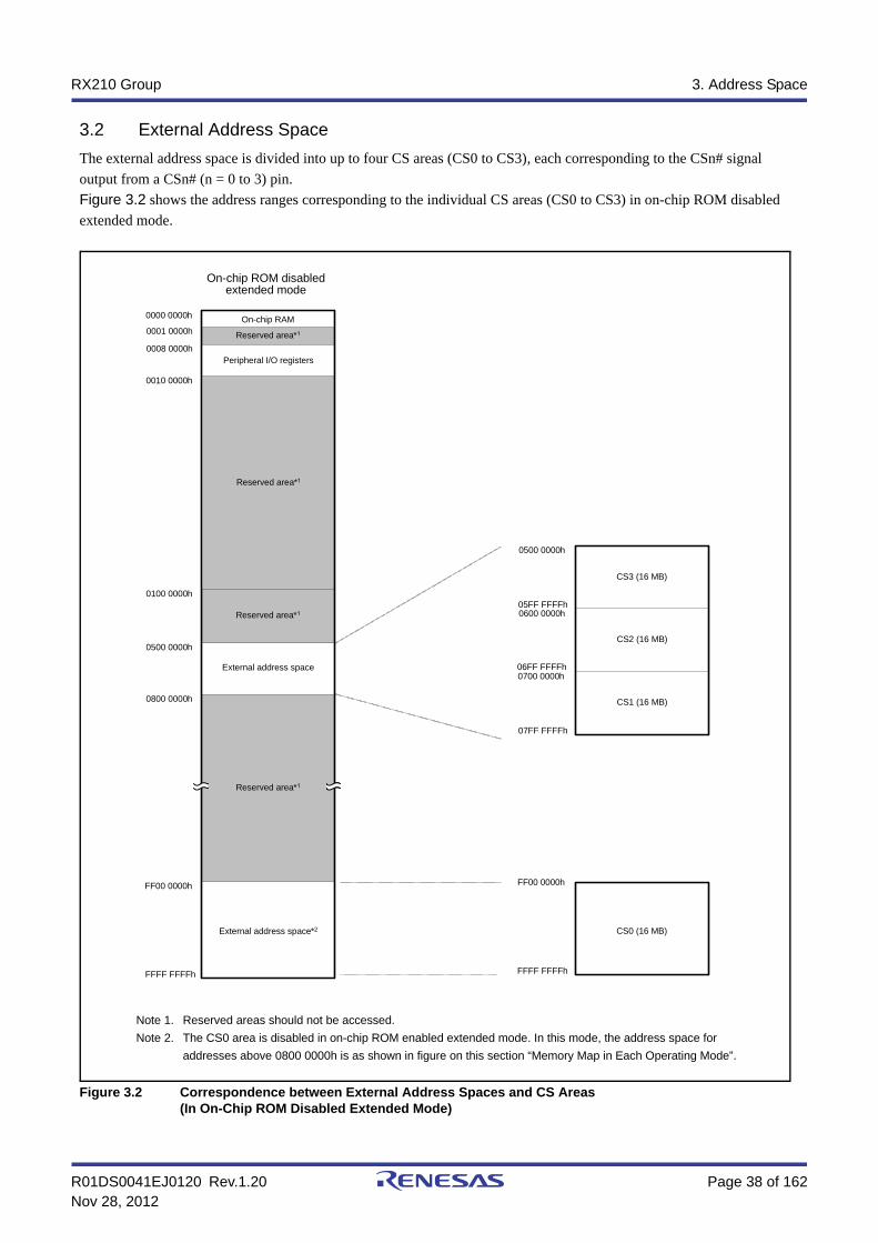
3.2 External Address Space
The external address space is divided into up to four CS areas (CS0 to CS3), each corresponding to the CSn# signal
output from a CSn# (n = 0 to 3) pin.
Figure 3.2 shows the address ranges corresponding to the individual CS areas (CS0 to CS3) in on-chip ROM disabled
extended mode.
Figure 3.2 Correspondence between External Address Spaces and CS Areas(In On-Chip ROM Disabled Extended Mode)
0500 0000h
0600 0000h
0700 0000h
CS3 (16 MB)
05FF FFFFh
06FF FFFFh
07FF FFFFh
CS2 (16 MB)
CS1 (16 MB)
FFFF FFFFh
FF00 0000h
CS0 (16 MB)
Note 1. Reserved areas should not be accessed.
Note 2. The CS0 area is disabled in on-chip ROM enabled extended mode. In this mode, the address space for
addresses above 0800 0000h is as shown in figure on this section “Memory Map in Each Operating Mode”.
Reserved area*1
Reserved area*1
Reserved area*1
Reserved area*1
0000 0000h
0008 0000h
FFFF FFFFh
On-chip ROM disabled extended mode
On-chip RAM
0010 0000h
Peripheral I/O registers
0100 0000h
0800 0000h
FF00 0000h
0001 0000h
External address space*2
External address space
0500 0000h
R01DS0041EJ0120 Rev.1.20 Page 39 of 162Nov 28, 2012
RX210 Group 4. I/O Registers
4. I/O RegistersThis section gives information on the on-chip I/O register addresses and bit configuration. The information is given as
shown below. Notes on writing to registers are also given at the end.
(1) I/O register addresses (address order)
Registers are listed from the lower allocation addresses.
Registers are classified according to module symbols.
Numbers of cycles for access indicate numbers of cycles of the given base clock.
Among the internal I/O register area, addresses not listed in the list of registers are reserved. Reserved addresses
must not be accessed. Do not access these addresses; otherwise, the operation when accessing these bits and
subsequent operations cannot be guaranteed.
(2) Notes on writing to I/O registers
When writing to an I/O register, the CPU starts executing the subsequent instruction before completing I/O register write.
This may cause the subsequent instruction to be executed before the post-update I/O register value is reflected on the
operation.
As described in the following examples, special care is required for the cases in which the subsequent instruction must be
executed after the post-update I/O register value is actually reflected.
[Examples of cases requiring special care]
The subsequent instruction must be executed while an interrupt request is disabled with the IENj bit in IERn of the
ICU (interrupt request enable bit) cleared to 0.
A WAIT instruction is executed immediately after the preprocessing for causing a transition to the low power
consumption state.
In the above cases, after writing to an I/O register, wait until the write operation is completed using the following
procedure and then execute the subsequent instruction.
(a) Write to an I/O register.
(b) Read the value from the I/O register to a general register.
(c) Execute the operation using the value read.
(d) Execute the subsequent instruction.
[Instruction examples]
Byte-size I/O registers
MOV.L #SFR_ADDR, R1
MOV.B #SFR_DATA, [R1]
CMP [R1].UB, R1
;; Next process
Word-size I/O registers
MOV.L #SFR_ADDR, R1
MOV.W #SFR_DATA, [R1]
CMP [R1].W, R1
;; Next process

R01DS0041EJ0120 Rev.1.20 Page 40 of 162Nov 28, 2012
RX210 Group 4. I/O Registers
Longword-size I/O registers
MOV.L #SFR_ADDR, R1
MOV.L #SFR_DATA, [R1]
CMP [R1].L, R1
;; Next process
If multiple registers are written to and a subsequent instruction should be executed after the write operations are entirely
completed, only read the I/O register that was last written to and execute the operation using the value; it is not necessary
to read or execute operation for all the registers that were written to.
(3) Number of Access Cycles to I/O Registers
For numbers of clock cycles for access to I/O registers, see Table 4.1, List of I/O Registers (Address Order).
The number of access cycles to I/O registers is obtained by following equation.*1
Number of access cycles to I/O registers = Number of bus cycles for internal main bus 1 +
Number of divided clock synchronization cycles +
Number of bus cycles for internal peripheral bus 1 to 6
The number of bus cycles of internal peripheral bus 1 to 6 differs according to the register to be accessed.
When peripheral functions connected to internal peripheral bus 2 to 6 or registers for the external bus control unit (except
for bus error related registers) are accessed, the number of divided clock synchronization cycles is added.
The number of divided clock synchronization cycles differs depending on the frequency ratio between ICLK and PCLK
(or FCLK, BCLK) or bus access timing.
In the peripheral function unit, when the frequency ratio of ICLK is equal to or greater than that of PCLK (or FCLK), the
sum of the number of bus cycles for internal main bus 1 and the number of the divided clock synchronization cycles will
be one cycle of PCLK (or FCLK) at a maximum. Therefore, one PCLK (or FCLK) has been added to the number of
access cycles shown in Table 4.1.
When the frequency ratio of ICLK is lower than that of PCLK (or FCLK), the subsequent bus access is started from the
ICLK cycle following the completion of the access to the peripheral functions. Therefore, the access cycles are described
on an ICLK basis.
In the external bus control unit, the sum of the number of bus cycles for internal main bus 1 and the number of divided
clock synchronization cycles will be one cycle of BCLK at a maximum. Therefore, one BCLK is added to the number of
access cycles shown in Table 4.1.
Note 1. This applies to the number of cycles when the access from the CPU does not conflict with the instruction fetching to the external memory or bus access from the different bus master (DMAC or DTC).
R01DS0041EJ0120 Rev.1.20 Page 41 of 162Nov 28, 2012
RX210 Group 4. I/O Registers
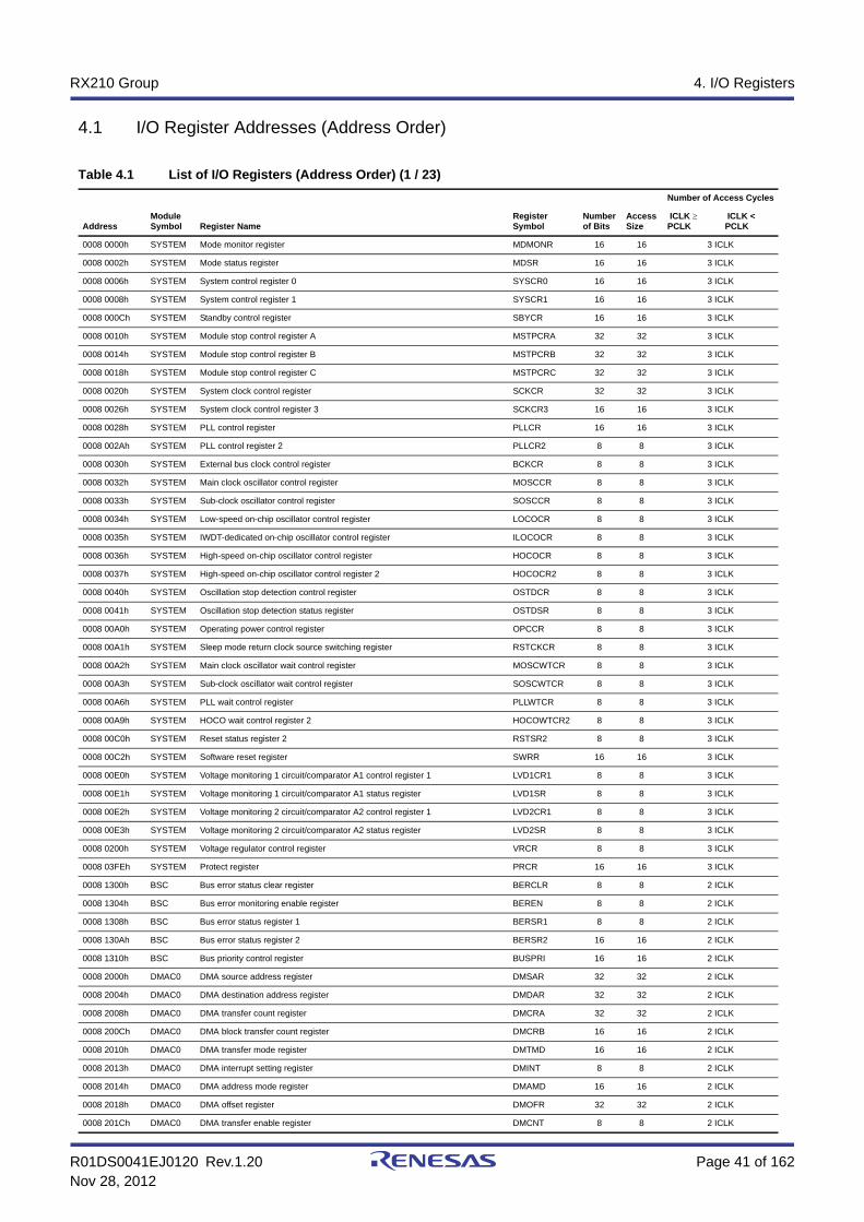
4.1 I/O Register Addresses (Address Order)
Table 4.1 List of I/O Registers (Address Order) (1 / 23)
AddressModule Symbol Register Name
Register Symbol
Number of Bits
Access Size
Number of Access Cycles
ICLK PCLK
ICLK <PCLK
0008 0000h SYSTEM Mode monitor register MDMONR 16 16 3 ICLK
0008 0002h SYSTEM Mode status register MDSR 16 16 3 ICLK
0008 0006h SYSTEM System control register 0 SYSCR0 16 16 3 ICLK
0008 0008h SYSTEM System control register 1 SYSCR1 16 16 3 ICLK
0008 000Ch SYSTEM Standby control register SBYCR 16 16 3 ICLK
0008 0010h SYSTEM Module stop control register A MSTPCRA 32 32 3 ICLK
0008 0014h SYSTEM Module stop control register B MSTPCRB 32 32 3 ICLK
0008 0018h SYSTEM Module stop control register C MSTPCRC 32 32 3 ICLK
0008 0020h SYSTEM System clock control register SCKCR 32 32 3 ICLK
0008 0026h SYSTEM System clock control register 3 SCKCR3 16 16 3 ICLK
0008 0028h SYSTEM PLL control register PLLCR 16 16 3 ICLK
0008 002Ah SYSTEM PLL control register 2 PLLCR2 8 8 3 ICLK
0008 0030h SYSTEM External bus clock control register BCKCR 8 8 3 ICLK
0008 0032h SYSTEM Main clock oscillator control register MOSCCR 8 8 3 ICLK
0008 0033h SYSTEM Sub-clock oscillator control register SOSCCR 8 8 3 ICLK
0008 0034h SYSTEM Low-speed on-chip oscillator control register LOCOCR 8 8 3 ICLK
0008 0035h SYSTEM IWDT-dedicated on-chip oscillator control register ILOCOCR 8 8 3 ICLK
0008 0036h SYSTEM High-speed on-chip oscillator control register HOCOCR 8 8 3 ICLK
0008 0037h SYSTEM High-speed on-chip oscillator control register 2 HOCOCR2 8 8 3 ICLK
0008 0040h SYSTEM Oscillation stop detection control register OSTDCR 8 8 3 ICLK
0008 0041h SYSTEM Oscillation stop detection status register OSTDSR 8 8 3 ICLK
0008 00A0h SYSTEM Operating power control register OPCCR 8 8 3 ICLK
0008 00A1h SYSTEM Sleep mode return clock source switching register RSTCKCR 8 8 3 ICLK
0008 00A2h SYSTEM Main clock oscillator wait control register MOSCWTCR 8 8 3 ICLK
0008 00A3h SYSTEM Sub-clock oscillator wait control register SOSCWTCR 8 8 3 ICLK
0008 00A6h SYSTEM PLL wait control register PLLWTCR 8 8 3 ICLK
0008 00A9h SYSTEM HOCO wait control register 2 HOCOWTCR2 8 8 3 ICLK
0008 00C0h SYSTEM Reset status register 2 RSTSR2 8 8 3 ICLK
0008 00C2h SYSTEM Software reset register SWRR 16 16 3 ICLK
0008 00E0h SYSTEM Voltage monitoring 1 circuit/comparator A1 control register 1 LVD1CR1 8 8 3 ICLK
0008 00E1h SYSTEM Voltage monitoring 1 circuit/comparator A1 status register LVD1SR 8 8 3 ICLK
0008 00E2h SYSTEM Voltage monitoring 2 circuit/comparator A2 control register 1 LVD2CR1 8 8 3 ICLK
0008 00E3h SYSTEM Voltage monitoring 2 circuit/comparator A2 status register LVD2SR 8 8 3 ICLK
0008 0200h SYSTEM Voltage regulator control register VRCR 8 8 3 ICLK
0008 03FEh SYSTEM Protect register PRCR 16 16 3 ICLK
0008 1300h BSC Bus error status clear register BERCLR 8 8 2 ICLK
0008 1304h BSC Bus error monitoring enable register BEREN 8 8 2 ICLK
0008 1308h BSC Bus error status register 1 BERSR1 8 8 2 ICLK
0008 130Ah BSC Bus error status register 2 BERSR2 16 16 2 ICLK
0008 1310h BSC Bus priority control register BUSPRI 16 16 2 ICLK
0008 2000h DMAC0 DMA source address register DMSAR 32 32 2 ICLK
0008 2004h DMAC0 DMA destination address register DMDAR 32 32 2 ICLK
0008 2008h DMAC0 DMA transfer count register DMCRA 32 32 2 ICLK
0008 200Ch DMAC0 DMA block transfer count register DMCRB 16 16 2 ICLK
0008 2010h DMAC0 DMA transfer mode register DMTMD 16 16 2 ICLK
0008 2013h DMAC0 DMA interrupt setting register DMINT 8 8 2 ICLK
0008 2014h DMAC0 DMA address mode register DMAMD 16 16 2 ICLK
0008 2018h DMAC0 DMA offset register DMOFR 32 32 2 ICLK
0008 201Ch DMAC0 DMA transfer enable register DMCNT 8 8 2 ICLK

R01DS0041EJ0120 Rev.1.20 Page 42 of 162Nov 28, 2012
RX210 Group 4. I/O Registers
0008 201Dh DMAC0 DMA software start register DMREQ 8 8 2 ICLK
0008 201Eh DMAC0 DMA status register DMSTS 8 8 2 ICLK
0008 201Fh DMAC0 DMA activation source flag control register DMCSL 8 8 2 ICLK
0008 2040h DMAC1 DMA source address register DMSAR 32 32 2 ICLK
0008 2044h DMAC1 DMA destination address register DMDAR 32 32 2 ICLK
0008 2048h DMAC1 DMA transfer count register DMCRA 32 32 2 ICLK
0008 204Ch DMAC1 DMA block transfer count register DMCRB 16 16 2 ICLK
0008 2050h DMAC1 DMA transfer mode register DMTMD 16 16 2 ICLK
0008 2053h DMAC1 DMA interrupt setting register DMINT 8 8 2 ICLK
0008 2054h DMAC1 DMA address mode register DMAMD 16 16 2 ICLK
0008 205Ch DMAC1 DMA transfer enable register DMCNT 8 8 2 ICLK
0008 205Dh DMAC1 DMA software start register DMREQ 8 8 2 ICLK
0008 205Eh DMAC1 DMA status register DMSTS 8 8 2 ICLK
0008 205Fh DMAC1 DMA activation source flag control register DMCSL 8 8 2 ICLK
0008 2080h DMAC2 DMA source address register DMSAR 32 32 2 ICLK
0008 2084h DMAC2 DMA destination address register DMDAR 32 32 2 ICLK
0008 2088h DMAC2 DMA transfer count register DMCRA 32 32 2 ICLK
0008 208Ch DMAC2 DMA block transfer count register DMCRB 16 16 2 ICLK
0008 2090h DMAC2 DMA transfer mode register DMTMD 16 16 2 ICLK
0008 2093h DMAC2 DMA interrupt setting register DMINT 8 8 2 ICLK
0008 2094h DMAC2 DMA address mode register DMAMD 16 16 2 ICLK
0008 209Ch DMAC2 DMA transfer enable register DMCNT 8 8 2 ICLK
0008 209Dh DMAC2 DMA software start register DMREQ 8 8 2 ICLK
0008 209Eh DMAC2 DMA status register DMSTS 8 8 2 ICLK
0008 209Fh DMAC2 DMA activation source flag control register DMCSL 8 8 2 ICLK
0008 20C0h DMAC3 DMA source address register DMSAR 32 32 2 ICLK
0008 20C4h DMAC3 DMA destination address register DMDAR 32 32 2 ICLK
0008 20C8h DMAC3 DMA transfer count register DMCRA 32 32 2 ICLK
0008 20CCh DMAC3 DMA block transfer count register DMCRB 16 16 2 ICLK
0008 20D0h DMAC3 DMA transfer mode register DMTMD 16 16 2 ICLK
0008 20D3h DMAC3 DMA interrupt setting register DMINT 8 8 2 ICLK
0008 20D4h DMAC3 DMA address mode register DMAMD 16 16 2 ICLK
0008 20DCh DMAC3 DMA transfer enable register DMCNT 8 8 2 ICLK
0008 20DDh DMAC3 DMA software start register DMREQ 8 8 2 ICLK
0008 20DEh DMAC3 DMA status register DMSTS 8 8 2 ICLK
0008 20DFh DMAC3 DMA activation source flag control register DMCSL 8 8 2 ICLK
0008 2200h DMAC DMA module activation register DMAST 8 8 2 ICLK
0008 2400h DTC DTC control register DTCCR 8 8 2 ICLK
0008 2404h DTC DTC vector base register DTCVBR 32 32 2 ICLK
0008 2408h DTC DTC address mode register DTCADMOD 8 8 2 ICLK
0008 240Ch DTC DTC module start register DTCST 8 8 2 ICLK
0008 240Eh DTC DTC status register DTCSTS 16 16 2 ICLK
0008 3002h BSC CS0 mode register CS0MOD 16 16 1, 2 BCLK
0008 3004h BSC CS0 wait control register 1 CS0WCR1 32 32 1, 2 BCLK
0008 3008h BSC CS0 wait control register 2 CS0WCR2 32 32 1, 2 BCLK
0008 3012h BSC CS1 mode register CS1MOD 16 16 1, 2 BCLK
0008 3014h BSC CS1 wait control register 1 CS1WCR1 32 32 1, 2 BCLK
0008 3018h BSC CS1 wait control register 2 CS1WCR2 32 32 1, 2 BCLK
0008 3022h BSC CS2 mode register CS2MOD 16 16 1, 2 BCLK
0008 3024h BSC CS2 wait control register 1 CS2WCR1 32 32 1, 2 BCLK
0008 3028h BSC CS2 wait control register 2 CS2WCR2 32 32 1, 2 BCLK
Table 4.1 List of I/O Registers (Address Order) (2 / 23)
AddressModule Symbol Register Name
Register Symbol
Number of Bits
Access Size
Number of Access Cycles
ICLK PCLK
ICLK <PCLK

R01DS0041EJ0120 Rev.1.20 Page 43 of 162Nov 28, 2012
RX210 Group 4. I/O Registers
0008 3032h BSC CS3 mode register CS3MOD 16 16 1, 2 BCLK
0008 3034h BSC CS3 wait control register 1 CS3WCR1 32 32 1, 2 BCLK
0008 3038h BSC CS3 wait control register 2 CS3WCR2 32 32 1, 2 BCLK
0008 3802h BSC CS0 control register CS0CR 16 16 1, 2 BCLK
0008 380Ah BSC CS0 recovery cycle register CS0REC 16 16 1, 2 BCLK
0008 3812h BSC CS1 control register CS1CR 16 16 1, 2 BCLK
0008 381Ah BSC CS1 recovery cycle register CS1REC 16 16 1, 2 BCLK
0008 3822h BSC CS2 control register CS2CR 16 16 1, 2 BCLK
0008 382Ah BSC CS2 recovery cycle register CS2REC 16 16 1, 2 BCLK
0008 3832h BSC CS3 control register CS3CR 16 16 1, 2 BCLK
0008 383Ah BSC CS3 recovery cycle register CS3REC 16 16 1, 2 BCLK
0008 3880h BSC CS recovery cycle insertion enable register CSRECEN 16 16 1, 2 BCLK
0008 7010h ICU Interrupt request register 016 IR016 8 8 2 ICLK
0008 7015h ICU Interrupt request register 021 IR021 8 8 2 ICLK
0008 7017h ICU Interrupt request register 023 IR023 8 8 2 ICLK
0008 701Bh ICU Interrupt request register 027 IR027 8 8 2 ICLK
0008 701Ch ICU Interrupt request register 028 IR028 8 8 2 ICLK
0008 701Dh ICU Interrupt request register 029 IR029 8 8 2 ICLK
0008 701Eh ICU Interrupt request register 030 IR030 8 8 2 ICLK
0008 701Fh ICU Interrupt request register 031 IR031 8 8 2 ICLK
0008 7020h ICU Interrupt request register 032 IR032 8 8 2 ICLK
0008 7021h ICU Interrupt request register 033 IR033 8 8 2 ICLK
0008 7022h ICU Interrupt request register 034 IR034 8 8 2 ICLK
0008 702Ch ICU Interrupt request register 044 IR044 8 8 2 ICLK
0008 702Dh ICU Interrupt request register 045 IR045 8 8 2 ICLK
0008 702Eh ICU Interrupt request register 046 IR046 8 8 2 ICLK
0008 702Fh ICU Interrupt request register 047 IR047 8 8 2 ICLK
0008 7039h ICU Interrupt request register 057 IR057 8 8 2 ICLK
0008 703Ah ICU Interrupt request register 058 IR058 8 8 2 ICLK
0008 703Bh ICU Interrupt request register 059 IR059 8 8 2 ICLK
0008 703Fh ICU Interrupt request register 063 IR063 8 8 2 ICLK
0008 7040h ICU Interrupt request register 064 IR064 8 8 2 ICLK
0008 7041h ICU Interrupt request register 065 IR065 8 8 2 ICLK
0008 7042h ICU Interrupt request register 066 IR066 8 8 2 ICLK
0008 7043h ICU Interrupt request register 067 IR067 8 8 2 ICLK
0008 7044h ICU Interrupt request register 068 IR068 8 8 2 ICLK
0008 7045h ICU Interrupt request register 069 IR069 8 8 2 ICLK
0008 7046h ICU Interrupt request register 070 IR070 8 8 2 ICLK
0008 7047h ICU Interrupt request register 071 IR071 8 8 2 ICLK
0008 7058h ICU Interrupt request register 088 IR088 8 8 2 ICLK
0008 7059h ICU Interrupt request register 089 IR089 8 8 2 ICLK
0008 705Ch ICU Interrupt request register 092 IR092 8 8 2 ICLK
0008 705Dh ICU Interrupt request register 093 IR093 8 8 2 ICLK
0008 7066h ICU Interrupt request register 102 IR102 8 8 2 ICLK
0008 7067h ICU Interrupt request register 103 IR103 8 8 2 ICLK
0008 706Ah ICU Interrupt request register 106 IR106 8 8 2 ICLK
0008 706Bh ICU Interrupt request register 107 IR107 8 8 2 ICLK
0008 7072h ICU Interrupt request register 114 IR114 8 8 2 ICLK
0008 7073h ICU Interrupt request register 115 IR115 8 8 2 ICLK
0008 7074h ICU Interrupt request register 116 IR116 8 8 2 ICLK
0008 7075h ICU Interrupt request register 117 IR117 8 8 2 ICLK
Table 4.1 List of I/O Registers (Address Order) (3 / 23)
AddressModule Symbol Register Name
Register Symbol
Number of Bits
Access Size
Number of Access Cycles
ICLK PCLK
ICLK <PCLK
R01DS0041EJ0120 Rev.1.20 Page 44 of 162Nov 28, 2012
RX210 Group 4. I/O Registers
0008 7076h ICU Interrupt request register 118 IR118 8 8 2 ICLK
0008 7077h ICU Interrupt request register 119 IR119 8 8 2 ICLK
0008 7078h ICU Interrupt request register 120 IR120 8 8 2 ICLK
0008 7079h ICU Interrupt request register 121 IR121 8 8 2 ICLK
0008 707Ah ICU Interrupt request register 122 IR122 8 8 2 ICLK
0008 707Bh ICU Interrupt request register 123 IR123 8 8 2 ICLK
0008 707Ch ICU Interrupt request register 124 IR124 8 8 2 ICLK
0008 707Dh ICU Interrupt request register 125 IR125 8 8 2 ICLK
0008 707Eh ICU Interrupt request register 126 IR126 8 8 2 ICLK
0008 707Fh ICU Interrupt request register 127 IR127 8 8 2 ICLK
0008 7080h ICU Interrupt request register 128 IR128 8 8 2 ICLK
0008 7081h ICU Interrupt request register 129 IR129 8 8 2 ICLK
0008 7082h ICU Interrupt request register 130 IR130 8 8 2 ICLK
0008 7083h ICU Interrupt request register 131 IR131 8 8 2 ICLK
0008 7084h ICU Interrupt request register 132 IR132 8 8 2 ICLK
0008 7085h ICU Interrupt request register 133 IR133 8 8 2 ICLK
0008 7086h ICU Interrupt request register 134 IR134 8 8 2 ICLK
0008 7087h ICU Interrupt request register 135 IR135 8 8 2 ICLK
0008 7088h ICU Interrupt request register 136 IR136 8 8 2 ICLK
0008 7089h ICU Interrupt request register 137 IR137 8 8 2 ICLK
0008 708Ah ICU Interrupt request register 138 IR138 8 8 2 ICLK
0008 708Bh ICU Interrupt request register 139 IR139 8 8 2 ICLK
0008 708Ch ICU Interrupt request register 140 IR140 8 8 2 ICLK
0008 708Dh ICU Interrupt request register 141 IR141 8 8 2 ICLK
0008 70AAh ICU Interrupt request register 170 IR170 8 8 2 ICLK
0008 70ABh ICU Interrupt request register 171 IR171 8 8 2 ICLK
0008 70AEh ICU Interrupt request register 174 IR174 8 8 2 ICLK
0008 70AFh ICU Interrupt request register 175 IR175 8 8 2 ICLK
0008 70B0h ICU Interrupt request register 176 IR176 8 8 2 ICLK
0008 70B1h ICU Interrupt request register 177 IR177 8 8 2 ICLK
0008 70B2h ICU Interrupt request register 178 IR178 8 8 2 ICLK
0008 70B3h ICU Interrupt request register 179 IR179 8 8 2 ICLK
0008 70B4h ICU Interrupt request register 180 IR180 8 8 2 ICLK
0008 70B5h ICU Interrupt request register 181 IR181 8 8 2 ICLK
0008 70B6h ICU Interrupt request register 182 IR182 8 8 2 ICLK
0008 70B7h ICU Interrupt request register 183 IR183 8 8 2 ICLK
0008 70B8h ICU Interrupt request register 184 IR184 8 8 2 ICLK
0008 70B9h ICU Interrupt request register 185 IR185 8 8 2 ICLK
0008 70C6h ICU Interrupt request register 198 IR198 8 8 2 ICLK
0008 70C7h ICU Interrupt request register 199 IR199 8 8 2 ICLK
0008 70C8h ICU Interrupt request register 200 IR200 8 8 2 ICLK
0008 70C9h ICU Interrupt request register 201 IR201 8 8 2 ICLK
0008 70D6h ICU Interrupt request register 214 IR214 8 8 2 ICLK
0008 70D7h ICU Interrupt request register 215 IR215 8 8 2 ICLK
0008 70D8h ICU Interrupt request register 216 IR216 8 8 2 ICLK
0008 70D9h ICU Interrupt request register 217 IR217 8 8 2 ICLK
0008 70DAh ICU Interrupt request register 218 IR218 8 8 2 ICLK
0008 70DBh ICU Interrupt request register 219 IR219 8 8 2 ICLK
0008 70DCh ICU Interrupt request register 220 IR220 8 8 2 ICLK
0008 70DDh ICU Interrupt request register 221 IR221 8 8 2 ICLK
0008 70DEh ICU Interrupt request register 222 IR222 8 8 2 ICLK
Table 4.1 List of I/O Registers (Address Order) (4 / 23)
AddressModule Symbol Register Name
Register Symbol
Number of Bits
Access Size
Number of Access Cycles
ICLK PCLK
ICLK <PCLK

R01DS0041EJ0120 Rev.1.20 Page 45 of 162Nov 28, 2012
RX210 Group 4. I/O Registers
0008 70DFh ICU Interrupt request register 223 IR223 8 8 2 ICLK
0008 70E0h ICU Interrupt request register 224 IR224 8 8 2 ICLK
0008 70E1h ICU Interrupt request register 225 IR225 8 8 2 ICLK
0008 70E2h ICU Interrupt request register 226 IR226 8 8 2 ICLK
0008 70E3h ICU Interrupt request register 227 IR227 8 8 2 ICLK
0008 70E4h ICU Interrupt request register 228 IR228 8 8 2 ICLK
0008 70E5h ICU Interrupt request register 229 IR229 8 8 2 ICLK
0008 70E6h ICU Interrupt request register 230 IR230 8 8 2 ICLK
0008 70E7h ICU Interrupt request register 231 IR231 8 8 2 ICLK
0008 70E8h ICU Interrupt request register 232 IR232 8 8 2 ICLK
0008 70E9h ICU Interrupt request register 233 IR233 8 8 2 ICLK
0008 70EAh ICU Interrupt request register 234 IR234 8 8 2 ICLK
0008 70EBh ICU Interrupt request register 235 IR235 8 8 2 ICLK
0008 70ECh ICU Interrupt request register 236 IR236 8 8 2 ICLK
0008 70EDh ICU Interrupt request register 237 IR237 8 8 2 ICLK
0008 70EEh ICU Interrupt request register 238 IR238 8 8 2 ICLK
0008 70EFh ICU Interrupt request register 239 IR239 8 8 2 ICLK
0008 70F0h ICU Interrupt request register 240 IR240 8 8 2 ICLK
0008 70F1h ICU Interrupt request register 241 IR241 8 8 2 ICLK
0008 70F2h ICU Interrupt request register 242 IR242 8 8 2 ICLK
0008 70F3h ICU Interrupt request register 243 IR243 8 8 2 ICLK
0008 70F4h ICU Interrupt request register 244 IR244 8 8 2 ICLK
0008 70F5h ICU Interrupt request register 245 IR245 8 8 2 ICLK
0008 70F6h ICU Interrupt request register 246 IR246 8 8 2 ICLK
0008 70F7h ICU Interrupt request register 247 IR247 8 8 2 ICLK
0008 70F8h ICU Interrupt request register 248 IR248 8 8 2 ICLK
0008 70F9h ICU Interrupt request register 249 IR249 8 8 2 ICLK
0008 711Bh ICU DTC activation enable register 027 DTCER027 8 8 2 ICLK
0008 711Ch ICU DTC activation enable register 028 DTCER028 8 8 2 ICLK
0008 711Dh ICU DTC activation enable register 029 DTCER029 8 8 2 ICLK
0008 711Eh ICU DTC activation enable register 030 DTCER030 8 8 2 ICLK
0008 711Fh ICU DTC activation enable register 031 DTCER031 8 8 2 ICLK
0008 712Dh ICU DTC activation enable register 045 DTCER045 8 8 2 ICLK
0008 712Eh ICU DTC activation enable register 046 DTCER046 8 8 2 ICLK
0008 713Ah ICU DTC activation enable register 058 DTCER058 8 8 2 ICLK
0008 713Bh ICU DTC activation enable register 059 DTCER059 8 8 2 ICLK
0008 7140h ICU DTC activation enable register 064 DTCER064 8 8 2 ICLK
0008 7141h ICU DTC activation enable register 065 DTCER065 8 8 2 ICLK
0008 7142h ICU DTC activation enable register 066 DTCER066 8 8 2 ICLK
0008 7143h ICU DTC activation enable register 067 DTCER067 8 8 2 ICLK
0008 7144h ICU DTC activation enable register 068 DTCER068 8 8 2 ICLK
0008 7145h ICU DTC activation enable register 069 DTCER069 8 8 2 ICLK
0008 7146h ICU DTC activation enable register 070 DTCER070 8 8 2 ICLK
0008 7147h ICU DTC activation enable register 071 DTCER071 8 8 2 ICLK
0008 7166h ICU DTC activation enable register 102 DTCER102 8 8 2 ICLK
0008 7167h ICU DTC activation enable register 103 DTCER103 8 8 2 ICLK
0008 716Ah ICU DTC activation enable register 106 DTCER106 8 8 2 ICLK
0008 716Bh ICU DTC activation enable register 107 DTCER107 8 8 2 ICLK
0008 7172h ICU DTC activation enable register 114 DTCER114 8 8 2 ICLK
0008 7173h ICU DTC activation enable register 115 DTCER115 8 8 2 ICLK
0008 7174h ICU DTC activation enable register 116 DTCER116 8 8 2 ICLK
Table 4.1 List of I/O Registers (Address Order) (5 / 23)
AddressModule Symbol Register Name
Register Symbol
Number of Bits
Access Size
Number of Access Cycles
ICLK PCLK
ICLK <PCLK

R01DS0041EJ0120 Rev.1.20 Page 46 of 162Nov 28, 2012
RX210 Group 4. I/O Registers
0008 7175h ICU DTC activation enable register 117 DTCER117 8 8 2 ICLK
0008 7179h ICU DTC activation enable register 121 DTCER121 8 8 2 ICLK
0008 717Ah ICU DTC activation enable register 122 DTCER122 8 8 2 ICLK
0008 717Dh ICU DTC activation enable register 125 DTCER125 8 8 2 ICLK
0008 717Eh ICU DTC activation enable register 126 DTCER126 8 8 2 ICLK
0008 7181h ICU DTC activation enable register 129 DTCER129 8 8 2 ICLK
0008 7182h ICU DTC activation enable register 130 DTCER130 8 8 2 ICLK
0008 7183h ICU DTC activation enable register 131 DTCER131 8 8 2 ICLK
0008 7184h ICU DTC activation enable register 132 DTCER132 8 8 2 ICLK
0008 7186h ICU DTC activation enable register 134 DTCER134 8 8 2 ICLK
0008 7187h ICU DTC activation enable register 135 DTCER135 8 8 2 ICLK
0008 7188h ICU DTC activation enable register 136 DTCER136 8 8 2 ICLK
0008 7189h ICU DTC activation enable register 137 DTCER137 8 8 2 ICLK
0008 718Ah ICU DTC activation enable register 138 DTCER138 8 8 2 ICLK
0008 718Bh ICU DTC activation enable register 139 DTCER139 8 8 2 ICLK
0008 718Ch ICU DTC activation enable register 140 DTCER140 8 8 2 ICLK
0008 718Dh ICU DTC activation enable register 141 DTCER141 8 8 2 ICLK
0008 71AEh ICU DTC activation enable register 174 DTCER174 8 8 2 ICLK
0008 71AFh ICU DTC activation enable register 175 DTCER175 8 8 2 ICLK
0008 71B1h ICU DTC activation enable register 177 DTCER177 8 8 2 ICLK
0008 71B2h ICU DTC activation enable register 178 DTCER178 8 8 2 ICLK
0008 71B4h ICU DTC activation enable register 180 DTCER180 8 8 2 ICLK
0008 71B5h ICU DTC activation enable register 181 DTCER181 8 8 2 ICLK
0008 71B7h ICU DTC activation enable register 183 DTCER183 8 8 2 ICLK
0008 71B8h ICU DTC activation enable register 184 DTCER184 8 8 2 ICLK
0008 71C6h ICU DTC activation enable register 198 DTCER198 8 8 2 ICLK
0008 71C7h ICU DTC activation enable register 199 DTCER199 8 8 2 ICLK
0008 71C8h ICU DTC activation enable register 200 DTCER200 8 8 2 ICLK
0008 71C9h ICU DTC activation enable register 201 DTCER201 8 8 2 ICLK
0008 71D7h ICU DTC activation enable register 215 DTCER215 8 8 2 ICLK
0008 71D8h ICU DTC activation enable register 216 DTCER216 8 8 2 ICLK
0008 71DBh ICU DTC activation enable register 219 DTCER219 8 8 2 ICLK
0008 71DCh ICU DTC activation enable register 220 DTCER220 8 8 2 ICLK
0008 71DFh ICU DTC activation enable register 223 DTCER223 8 8 2 ICLK
0008 71E0h ICU DTC activation enable register 224 DTCER224 8 8 2 ICLK
0008 71E3h ICU DTC activation enable register 227 DTCER227 8 8 2 ICLK
0008 71E4h ICU DTC activation enable register 228 DTCER228 8 8 2 ICLK
0008 71E7h ICU DTC activation enable register 231 DTCER231 8 8 2 ICLK
0008 71E8h ICU DTC activation enable register 232 DTCER232 8 8 2 ICLK
0008 71EBh ICU DTC activation enable register 235 DTCER235 8 8 2 ICLK
0008 71ECh ICU DTC activation enable register 236 DTCER236 8 8 2 ICLK
0008 71EFh ICU DTC activation enable register 239 DTCER239 8 8 2 ICLK
0008 71F0h ICU DTC activation enable register 240 DTCER240 8 8 2 ICLK
0008 71F7h ICU DTC activation enable register 247 DTCER247 8 8 2 ICLK
0008 71F8h ICU DTC activation enable register 248 DTCER248 8 8 2 ICLK
0008 7202h ICU Interrupt request enable register 02 IER02 8 8 2 ICLK
0008 7203h ICU Interrupt request enable register 03 IER03 8 8 2 ICLK
0008 7204h ICU Interrupt request enable register 04 IER04 8 8 2 ICLK
0008 7205h ICU Interrupt request enable register 05 IER05 8 8 2 ICLK
0008 7207h ICU Interrupt request enable register 07 IER07 8 8 2 ICLK
0008 7208h ICU Interrupt request enable register 08 IER08 8 8 2 ICLK
Table 4.1 List of I/O Registers (Address Order) (6 / 23)
AddressModule Symbol Register Name
Register Symbol
Number of Bits
Access Size
Number of Access Cycles
ICLK PCLK
ICLK <PCLK

R01DS0041EJ0120 Rev.1.20 Page 47 of 162Nov 28, 2012
RX210 Group 4. I/O Registers
0008 720Bh ICU Interrupt request enable register 0B IER0B 8 8 2 ICLK
0008 720Ch ICU Interrupt request enable register 0C IER0C 8 8 2 ICLK
0008 720Dh ICU Interrupt request enable register 0D IER0D 8 8 2 ICLK
0008 720Eh ICU Interrupt request enable register 0E IER0E 8 8 2 ICLK
0008 720Fh ICU Interrupt request enable register 0F IER0F 8 8 2 ICLK
0008 7210h ICU Interrupt request enable register 10 IER10 8 8 2 ICLK
0008 7211h ICU Interrupt request enable register 11 IER11 8 8 2 ICLK
0008 7215h ICU Interrupt request enable register 15 IER15 8 8 2 ICLK
0008 7216h ICU Interrupt request enable register 16 IER16 8 8 2 ICLK
0008 7217h ICU Interrupt request enable register 17 IER17 8 8 2 ICLK
0008 7218h ICU Interrupt request enable register 18 IER18 8 8 2 ICLK
0008 7219h ICU Interrupt request enable register 19 IER19 8 8 2 ICLK
0008 721Ah ICU Interrupt request enable register 1A IER1A 8 8 2 ICLK
0008 721Bh ICU Interrupt request enable register 1B IER1B 8 8 2 ICLK
0008 721Ch ICU Interrupt request enable register 1C IER1C 8 8 2 ICLK
0008 721Dh ICU Interrupt request enable register 1D IER1D 8 8 2 ICLK
0008 721Eh ICU Interrupt request enable register 1E IER1E 8 8 2 ICLK
0008 721Fh ICU Interrupt request enable register 1F IER1F 8 8 2 ICLK
0008 72E0h ICU Software interrupt activation register SWINTR 8 8 2 ICLK
0008 72F0h ICU Fast interrupt set register FIR 16 16 2 ICLK
0008 7300h ICU Interrupt source priority register 000 IPR000 8 8 2 ICLK
0008 7301h ICU Interrupt source priority register 001 IPR001 8 8 2 ICLK
0008 7302h ICU Interrupt source priority register 002 IPR002 8 8 2 ICLK
0008 7303h ICU Interrupt source priority register 003 IPR003 8 8 2 ICLK
0008 7304h ICU Interrupt source priority register 004 IPR004 8 8 2 ICLK
0008 7305h ICU Interrupt source priority register 005 IPR005 8 8 2 ICLK
0008 7306h ICU Interrupt source priority register 006 IPR006 8 8 2 ICLK
0008 7307h ICU Interrupt source priority register 007 IPR007 8 8 2 ICLK
0008 7320h ICU Interrupt source priority register 032 IPR032 8 8 2 ICLK
0008 7321h ICU Interrupt source priority register 033 IPR033 8 8 2 ICLK
0008 7322h ICU Interrupt source priority register 034 IPR034 8 8 2 ICLK
0008 732Ch ICU Interrupt source priority register 044 IPR044 8 8 2 ICLK
0008 7339h ICU Interrupt source priority register 057 IPR057 8 8 2 ICLK
0008 733Ah ICU Interrupt source priority register 058 IPR058 8 8 2 ICLK
0008 733Bh ICU Interrupt source priority register 059 IPR059 8 8 2 ICLK
0008 733Fh ICU Interrupt source priority register 063 IPR063 8 8 2 ICLK
0008 7340h ICU Interrupt source priority register 064 IPR064 8 8 2 ICLK
0008 7341h ICU Interrupt source priority register 065 IPR065 8 8 2 ICLK
0008 7342h ICU Interrupt source priority register 066 IPR066 8 8 2 ICLK
0008 7343h ICU Interrupt source priority register 067 IPR067 8 8 2 ICLK
0008 7344h ICU Interrupt source priority register 068 IPR068 8 8 2 ICLK
0008 7345h ICU Interrupt source priority register 069 IPR069 8 8 2 ICLK
0008 7346h ICU Interrupt source priority register 070 IPR070 8 8 2 ICLK
0008 7347h ICU Interrupt source priority register 071 IPR071 8 8 2 ICLK
0008 7358h ICU Interrupt source priority register 088 IPR088 8 8 2 ICLK
0008 7359h ICU Interrupt source priority register 089 IPR089 8 8 2 ICLK
0008 735Ch ICU Interrupt source priority register 092 IPR092 8 8 2 ICLK
0008 735Dh ICU Interrupt source priority register 093 IPR093 8 8 2 ICLK
0008 7366h ICU Interrupt source priority register 102 IPR102 8 8 2 ICLK
0008 7367h ICU Interrupt source priority register 103 IPR103 8 8 2 ICLK
0008 736Ah ICU Interrupt source priority register 106 IPR106 8 8 2 ICLK
Table 4.1 List of I/O Registers (Address Order) (7 / 23)
AddressModule Symbol Register Name
Register Symbol
Number of Bits
Access Size
Number of Access Cycles
ICLK PCLK
ICLK <PCLK

R01DS0041EJ0120 Rev.1.20 Page 48 of 162Nov 28, 2012
RX210 Group 4. I/O Registers
0008 736Bh ICU Interrupt source priority register 107 IPR107 8 8 2 ICLK
0008 7372h ICU Interrupt source priority register 114 IPR114 8 8 2 ICLK
0008 7376h ICU Interrupt source priority register 118 IPR118 8 8 2 ICLK
0008 7379h ICU Interrupt source priority register 121 IPR121 8 8 2 ICLK
0008 737Bh ICU Interrupt source priority register 123 IPR123 8 8 2 ICLK
0008 737Dh ICU Interrupt source priority register 125 IPR125 8 8 2 ICLK
0008 737Fh ICU Interrupt source priority register 127 IPR127 8 8 2 ICLK
0008 7381h ICU Interrupt source priority register 129 IPR129 8 8 2 ICLK
0008 7385h ICU Interrupt source priority register 133 IPR133 8 8 2 ICLK
0008 7386h ICU Interrupt source priority register 134 IPR134 8 8 2 ICLK
0008 738Ah ICU Interrupt source priority register 138 IPR138 8 8 2 ICLK
0008 738Bh ICU Interrupt source priority register 139 IPR139 8 8 2 ICLK
0008 73AAh ICU Interrupt source priority register 170 IPR170 8 8 2 ICLK
0008 73ABh ICU Interrupt source priority register 171 IPR171 8 8 2 ICLK
0008 73AEh ICU Interrupt source priority register 174 IPR174 8 8 2 ICLK
0008 73B1h ICU Interrupt source priority register 177 IPR177 8 8 2 ICLK
0008 73B4h ICU Interrupt source priority register 180 IPR180 8 8 2 ICLK
0008 73B7h ICU Interrupt source priority register 183 IPR183 8 8 2 ICLK
0008 73C6h ICU Interrupt source priority register 198 IPR198 8 8 2 ICLK
0008 73C7h ICU Interrupt source priority register 199 IPR199 8 8 2 ICLK
0008 73C8h ICU Interrupt source priority register 200 IPR200 8 8 2 ICLK
0008 73C9h ICU Interrupt source priority register 201 IPR201 8 8 2 ICLK
0008 73D6h ICU Interrupt source priority register 214 IPR214 8 8 2 ICLK
0008 73DAh ICU Interrupt source priority register 218 IPR218 8 8 2 ICLK
0008 73DEh ICU Interrupt source priority register 222 IPR222 8 8 2 ICLK
0008 73E2h ICU Interrupt source priority register 226 IPR226 8 8 2 ICLK
0008 73E6h ICU Interrupt source priority register 230 IPR230 8 8 2 ICLK
0008 73EAh ICU Interrupt source priority register 234 IPR234 8 8 2 ICLK
0008 73EEh ICU Interrupt source priority register 238 IPR238 8 8 2 ICLK
0008 73F2h ICU Interrupt source priority register 242 IPR242 8 8 2 ICLK
0008 73F3h ICU Interrupt source priority register 243 IPR243 8 8 2 ICLK
0008 73F4h ICU Interrupt source priority register 244 IPR244 8 8 2 ICLK
0008 73F5h ICU Interrupt source priority register 245 IPR245 8 8 2 ICLK
0008 73F6h ICU Interrupt source priority register 246 IPR246 8 8 2 ICLK
0008 73F7h ICU Interrupt source priority register 247 IPR247 8 8 2 ICLK
0008 73F8h ICU Interrupt source priority register 248 IPR248 8 8 2 ICLK
0008 73F9h ICU Interrupt source priority register 249 IPR249 8 8 2 ICLK
0008 7400h ICU DMAC activation request select register 0 DMRSR0 8 8 2 ICLK
0008 7404h ICU DMAC activation request select register 1 DMRSR1 8 8 2 ICLK
0008 7408h ICU DMAC activation request select register 2 DMRSR2 8 8 2 ICLK
0008 740Ch ICU DMAC activation request select register 3 DMRSR3 8 8 2 ICLK
0008 7500h ICU IRQ control register 0 IRQCR0 8 8 2 ICLK
0008 7501h ICU IRQ control register 1 IRQCR1 8 8 2 ICLK
0008 7502h ICU IRQ control register 2 IRQCR2 8 8 2 ICLK
0008 7503h ICU IRQ control register 3 IRQCR3 8 8 2 ICLK
0008 7504h ICU IRQ control register 4 IRQCR4 8 8 2 ICLK
0008 7505h ICU IRQ control register 5 IRQCR5 8 8 2 ICLK
0008 7506h ICU IRQ control register 6 IRQCR6 8 8 2 ICLK
0008 7507h ICU IRQ control register 7 IRQCR7 8 8 2 ICLK
0008 7510h ICU IRQ pin digital filter enable register 0 IRQFLTE0 8 8 2 ICLK
0008 7514h ICU IRQ pin digital filter setting register 0 IRQFLTC0 16 16 2 ICLK
Table 4.1 List of I/O Registers (Address Order) (8 / 23)
AddressModule Symbol Register Name
Register Symbol
Number of Bits
Access Size
Number of Access Cycles
ICLK PCLK
ICLK <PCLK

R01DS0041EJ0120 Rev.1.20 Page 49 of 162Nov 28, 2012
RX210 Group 4. I/O Registers
0008 7580h ICU Non-maskable interrupt status register NMISR 8 8 2 ICLK
0008 7581h ICU Non-maskable interrupt enable register NMIER 8 8 2 ICLK
0008 7582h ICU Non-maskable interrupt clear register NMICLR 8 8 2 ICLK
0008 7583h ICU NMI pin interrupt control register NMICR 8 8 2 ICLK
0008 7590h ICU NMI pin digital filter enable register NMIFLTE 8 8 2 ICLK
0008 7594h ICU NMI pin digital filter setting register NMIFLTC 8 8 2 ICLK
0008 8000h CMT Compare match timer start register 0 CMSTR0 16 16 2, 3 PCLKB 2 ICLK
0008 8002h CMT0 Compare match timer control register CMCR 16 16 2, 3 PCLKB 2 ICLK
0008 8004h CMT0 Compare match timer counter CMCNT 16 16 2, 3 PCLKB 2 ICLK
0008 8006h CMT0 Compare match timer constant register CMCOR 16 16 2, 3 PCLKB 2 ICLK
0008 8008h CMT1 Compare match timer control register CMCR 16 16 2, 3 PCLKB 2 ICLK
0008 800Ah CMT1 Compare match timer counter CMCNT 16 16 2, 3 PCLKB 2 ICLK
0008 800Ch CMT1 Compare match timer constant register CMCOR 16 16 2, 3 PCLKB 2 ICLK
0008 8010h CMT Compare match timer start register 1 CMSTR1 16 16 2, 3 PCLKB 2 ICLK
0008 8012h CMT2 Compare match timer control register CMCR 16 16 2, 3 PCLKB 2 ICLK
0008 8014h CMT2 Compare match timer counter CMCNT 16 16 2, 3 PCLKB 2 ICLK
0008 8016h CMT2 Compare match timer constant register CMCOR 16 16 2, 3 PCLKB 2 ICLK
0008 8018h CMT3 Compare match timer control register CMCR 16 16 2, 3 PCLKB 2 ICLK
0008 801Ah CMT3 Compare match timer counter CMCNT 16 16 2, 3 PCLKB 2 ICLK
0008 801Ch CMT3 Compare match timer constant register CMCOR 16 16 2, 3 PCLKB 2 ICLK
0008 8020h WDT WDT refresh register WDTRR 8 8 2, 3 PCLKB 2 ICLK
0008 8022h WDT WDT control register WDTCR 16 16 2, 3 PCLKB 2 ICLK
0008 8024h WDT WDT status register WDTSR 16 16 2, 3 PCLKB 2 ICLK
0008 8026h WDT WDT reset control register WDTRCR 8 8 2, 3 PCLKB 2 ICLK
0008 8030h IWDT IWDT refresh register IWDTRR 8 8 2, 3 PCLKB 2 ICLK
0008 8032h IWDT IWDT control register IWDTCR 16 16 2, 3 PCLKB 2 ICLK
0008 8034h IWDT IWDT status register IWDTSR 16 16 2, 3 PCLKB 2 ICLK
0008 8036h IWDT IWDT reset control register IWDTRCR 8 8 2, 3 PCLKB 2 ICLK
0008 8038h IWDT IWDT count stop control register IWDTCSTPR 8 8 2, 3 PCLKB 2 ICLK
0008 80C0h DA D/A data register 0 DADR0 16 16 2, 3 PCLKB 2 ICLK
0008 80C2h DA D/A data register 1 DADR1 16 16 2, 3 PCLKB 2 ICLK
0008 80C4h DA D/A control register DACR 8 8 2, 3 PCLKB 2 ICLK
0008 80C5h DA DADRm format select register DADPR 8 8 2, 3 PCLKB 2 ICLK
0008 8200h TMR0 Timer control register TCR 8 8 2, 3 PCLKB 2 ICLK
0008 8201h TMR1 Timer counter control register TCR 8 8 2, 3 PCLKB 2 ICLK
0008 8202h TMR0 Timer control/status register TCSR 8 8 2, 3 PCLKB 2 ICLK
0008 8203h TMR1 Timer control/status register TCSR 8 8 2, 3 PCLKB 2 ICLK
0008 8204h TMR0 Time constant register A TCORA 8 8 2, 3 PCLKB 2 ICLK
0008 8205h TMR1 Time constant register A TCORA 8 8*1 2, 3 PCLKB 2 ICLK
0008 8206h TMR0 Time constant register B TCORB 8 8 2, 3 PCLKB 2 ICLK
0008 8207h TMR1 Time constant register B TCORB 8 8*1 2, 3 PCLKB 2 ICLK
0008 8208h TMR0 Timer counter TCNT 8 8 2, 3 PCLKB 2 ICLK
0008 8209h TMR1 Timer counter TCNT 8 8*1 2, 3 PCLKB 2 ICLK
0008 820Ah TMR0 Timer counter control register TCCR 8 8 2, 3 PCLKB 2 ICLK
0008 820Bh TMR1 Timer counter control register TCCR 8 8*1 2, 3 PCLKB 2 ICLK
0008 820Ch TMR0 Time count start register TCSTR 8 8 2, 3 PCLKB 2 ICLK
0008 8210h TMR2 Timer control register TCR 8 8 2, 3 PCLKB 2 ICLK
0008 8211h TMR3 Timer control register TCR 8 8 2, 3 PCLKB 2 ICLK
0008 8212h TMR2 Timer control/status register TCSR 8 8 2, 3 PCLKB 2 ICLK
0008 8213h TMR3 Timer control/status register TCSR 8 8 2, 3 PCLKB 2 ICLK
0008 8214h TMR2 Time constant register A TCORA 8 8 2, 3 PCLKB 2 ICLK
Table 4.1 List of I/O Registers (Address Order) (9 / 23)
AddressModule Symbol Register Name
Register Symbol
Number of Bits
Access Size
Number of Access Cycles
ICLK PCLK
ICLK <PCLK

R01DS0041EJ0120 Rev.1.20 Page 50 of 162Nov 28, 2012
RX210 Group 4. I/O Registers
0008 8215h TMR3 Time constant register A TCORA 8 8*1 2, 3 PCLKB 2 ICLK
0008 8216h TMR2 Time constant register B TCORB 8 8 2, 3 PCLKB 2 ICLK
0008 8217h TMR3 Time constant register B TCORB 8 8*1 2, 3 PCLKB 2 ICLK
0008 8218h TMR2 Timer counter TCNT 8 8 2, 3 PCLKB 2 ICLK
0008 8219h TMR3 Timer counter TCNT 8 8*1 2, 3 PCLKB 2 ICLK
0008 821Ah TMR2 Timer counter control register TCCR 8 8 2, 3 PCLKB 2 ICLK
0008 821Bh TMR3 Timer counter control register TCCR 8 8*1 2, 3 PCLKB 2 ICLK
0008 821Ch TMR2 Time count start register TCSTR 8 8 2, 3 PCLKB 2 ICLK
0008 8280h CRC CRC control register CRCCR 8 8 2, 3 PCLKB 2 ICLK
0008 8281h CRC CRC data input register CRCDIR 8 8 2, 3 PCLKB 2 ICLK
0008 8282h CRC CRC data output register CRCDOR 16 16 2, 3 PCLKB 2 ICLK
0008 8300h RIIC0 I2C bus control register 1 ICCR1 8 8 2, 3 PCLKB 2 ICLK
0008 8301h RIIC0 I2C bus control register 2 ICCR2 8 8 2, 3 PCLKB 2 ICLK
0008 8302h RIIC0 I2C bus mode register 1 ICMR1 8 8 2, 3 PCLKB 2 ICLK
0008 8303h RIIC0 I2C bus mode register 2 ICMR2 8 8 2, 3 PCLKB 2 ICLK
0008 8304h RIIC0 I2C bus mode register 3 ICMR3 8 8 2, 3 PCLKB 2 ICLK
0008 8305h RIIC0 I2C bus function enable register ICFER 8 8 2, 3 PCLKB 2 ICLK
0008 8306h RIIC0 I2C bus status enable register ICSER 8 8 2, 3 PCLKB 2 ICLK
0008 8307h RIIC0 I2C bus interrupt enable register ICIER 8 8 2, 3 PCLKB 2 ICLK
0008 8308h RIIC0 I2C bus status register 1 ICSR1 8 8 2, 3 PCLKB 2 ICLK
0008 8309h RIIC0 I2C bus status register 2 ICSR2 8 8 2, 3 PCLKB 2 ICLK
0008 830Ah RIIC0 Slave address register L0 SARL0 8 8 2, 3 PCLKB 2 ICLK
0008 830Ah RIIC0 Timeout internal counter L TMOCNTL 8 8 2, 3 PCLKB 2 ICLK
0008 830Bh RIIC0 Slave address register U0 SARU0 8 8 2, 3 PCLKB 2 ICLK
0008 830Bh RIIC0 Timeout internal counter U TMOCNTU 8 8*2 2, 3 PCLKB 2 ICLK
0008 830Ch RIIC0 Slave address register L1 SARL1 8 8 2, 3 PCLKB 2 ICLK
0008 830Dh RIIC0 Slave address register U1 SARU1 8 8 2, 3 PCLKB 2 ICLK
0008 830Eh RIIC0 Slave address register L2 SARL2 8 8 2, 3 PCLKB 2 ICLK
0008 830Fh RIIC0 Slave address register U2 SARU2 8 8 2, 3 PCLKB 2 ICLK
0008 8310h RIIC0 I2C bus bit rate low-level register ICBRL 8 8 2, 3 PCLKB 2 ICLK
0008 8311h RIIC0 I2C bus bit rate high-level register ICBRH 8 8 2, 3 PCLKB 2 ICLK
0008 8312h RIIC0 I2C bus transmit data register ICDRT 8 8 2, 3 PCLKB 2 ICLK
0008 8313h RIIC0 I2C bus receive data register ICDRR 8 8 2, 3 PCLKB 2 ICLK
0008 8380h RSPI0 RSPI control register SPCR 8 8 2, 3 PCLKB 2 ICLK
0008 8381h RSPI0 RSPI slave select polarity register SSLP 8 8 2, 3 PCLKB 2 ICLK
0008 8382h RSPI0 RSPI pin control register SPPCR 8 8 2, 3 PCLKB 2 ICLK
0008 8383h RSPI0 RSPI status register SPSR 8 8 2, 3 PCLKB 2 ICLK
0008 8384h RSPI0 RSPI data register SPDR 32 16, 32 2, 3 PCLKB 2 ICLK
0008 8388h RSPI0 RSPI sequence control register SPSCR 8 8 2, 3 PCLKB 2 ICLK
0008 8389h RSPI0 RSPI sequence status register SPSSR 8 8 2, 3 PCLKB 2 ICLK
0008 838Ah RSPI0 RSPI bit rate register SPBR 8 8 2, 3 PCLKB 2 ICLK
0008 838Bh RSPI0 RSPI data control register SPDCR 8 8 2, 3 PCLKB 2 ICLK
0008 838Ch RSPI0 RSPI clock delay register SPCKD 8 8 2, 3 PCLKB 2 ICLK
0008 838Dh RSPI0 RSPI slave select negation delay register SSLND 8 8 2, 3 PCLKB 2 ICLK
0008 838Eh RSPI0 RSPI next-access delay register SPND 8 8 2, 3 PCLKB 2 ICLK
0008 838Fh RSPI0 RSPI control register 2 SPCR2 8 8 2, 3 PCLKB 2 ICLK
0008 8390h RSPI0 RSPI command register 0 SPCMD0 16 16 2, 3 PCLKB 2 ICLK
0008 8392h RSPI0 RSPI command register 1 SPCMD1 16 16 2, 3 PCLKB 2 ICLK
0008 8394h RSPI0 RSPI command register 2 SPCMD2 16 16 2, 3 PCLKB 2 ICLK
0008 8396h RSPI0 RSPI command register 3 SPCMD3 16 16 2, 3 PCLKB 2 ICLK
0008 8398h RSPI0 RSPI command register 4 SPCMD4 16 16 2, 3 PCLKB 2 ICLK
Table 4.1 List of I/O Registers (Address Order) (10 / 23)
AddressModule Symbol Register Name
Register Symbol
Number of Bits
Access Size
Number of Access Cycles
ICLK PCLK
ICLK <PCLK
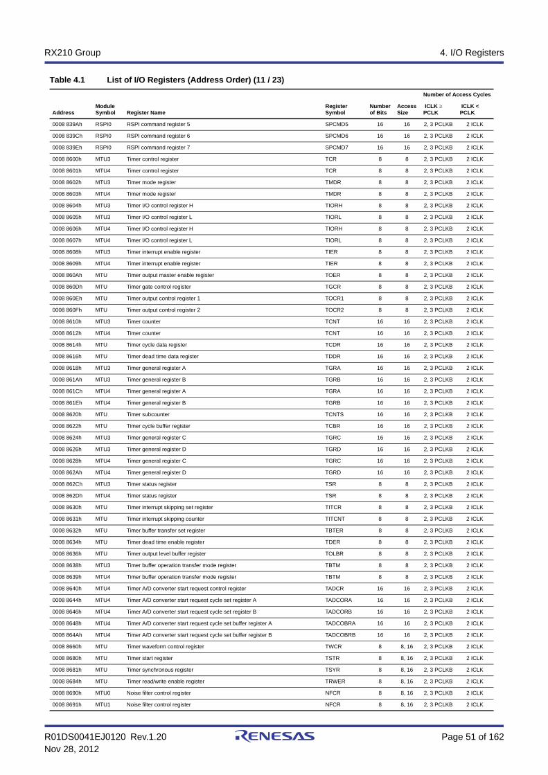
R01DS0041EJ0120 Rev.1.20 Page 51 of 162Nov 28, 2012
RX210 Group 4. I/O Registers
0008 839Ah RSPI0 RSPI command register 5 SPCMD5 16 16 2, 3 PCLKB 2 ICLK
0008 839Ch RSPI0 RSPI command register 6 SPCMD6 16 16 2, 3 PCLKB 2 ICLK
0008 839Eh RSPI0 RSPI command register 7 SPCMD7 16 16 2, 3 PCLKB 2 ICLK
0008 8600h MTU3 Timer control register TCR 8 8 2, 3 PCLKB 2 ICLK
0008 8601h MTU4 Timer control register TCR 8 8 2, 3 PCLKB 2 ICLK
0008 8602h MTU3 Timer mode register TMDR 8 8 2, 3 PCLKB 2 ICLK
0008 8603h MTU4 Timer mode register TMDR 8 8 2, 3 PCLKB 2 ICLK
0008 8604h MTU3 Timer I/O control register H TIORH 8 8 2, 3 PCLKB 2 ICLK
0008 8605h MTU3 Timer I/O control register L TIORL 8 8 2, 3 PCLKB 2 ICLK
0008 8606h MTU4 Timer I/O control register H TIORH 8 8 2, 3 PCLKB 2 ICLK
0008 8607h MTU4 Timer I/O control register L TIORL 8 8 2, 3 PCLKB 2 ICLK
0008 8608h MTU3 Timer interrupt enable register TIER 8 8 2, 3 PCLKB 2 ICLK
0008 8609h MTU4 Timer interrupt enable register TIER 8 8 2, 3 PCLKB 2 ICLK
0008 860Ah MTU Timer output master enable register TOER 8 8 2, 3 PCLKB 2 ICLK
0008 860Dh MTU Timer gate control register TGCR 8 8 2, 3 PCLKB 2 ICLK
0008 860Eh MTU Timer output control register 1 TOCR1 8 8 2, 3 PCLKB 2 ICLK
0008 860Fh MTU Timer output control register 2 TOCR2 8 8 2, 3 PCLKB 2 ICLK
0008 8610h MTU3 Timer counter TCNT 16 16 2, 3 PCLKB 2 ICLK
0008 8612h MTU4 Timer counter TCNT 16 16 2, 3 PCLKB 2 ICLK
0008 8614h MTU Timer cycle data register TCDR 16 16 2, 3 PCLKB 2 ICLK
0008 8616h MTU Timer dead time data register TDDR 16 16 2, 3 PCLKB 2 ICLK
0008 8618h MTU3 Timer general register A TGRA 16 16 2, 3 PCLKB 2 ICLK
0008 861Ah MTU3 Timer general register B TGRB 16 16 2, 3 PCLKB 2 ICLK
0008 861Ch MTU4 Timer general register A TGRA 16 16 2, 3 PCLKB 2 ICLK
0008 861Eh MTU4 Timer general register B TGRB 16 16 2, 3 PCLKB 2 ICLK
0008 8620h MTU Timer subcounter TCNTS 16 16 2, 3 PCLKB 2 ICLK
0008 8622h MTU Timer cycle buffer register TCBR 16 16 2, 3 PCLKB 2 ICLK
0008 8624h MTU3 Timer general register C TGRC 16 16 2, 3 PCLKB 2 ICLK
0008 8626h MTU3 Timer general register D TGRD 16 16 2, 3 PCLKB 2 ICLK
0008 8628h MTU4 Timer general register C TGRC 16 16 2, 3 PCLKB 2 ICLK
0008 862Ah MTU4 Timer general register D TGRD 16 16 2, 3 PCLKB 2 ICLK
0008 862Ch MTU3 Timer status register TSR 8 8 2, 3 PCLKB 2 ICLK
0008 862Dh MTU4 Timer status register TSR 8 8 2, 3 PCLKB 2 ICLK
0008 8630h MTU Timer interrupt skipping set register TITCR 8 8 2, 3 PCLKB 2 ICLK
0008 8631h MTU Timer interrupt skipping counter TITCNT 8 8 2, 3 PCLKB 2 ICLK
0008 8632h MTU Timer buffer transfer set register TBTER 8 8 2, 3 PCLKB 2 ICLK
0008 8634h MTU Timer dead time enable register TDER 8 8 2, 3 PCLKB 2 ICLK
0008 8636h MTU Timer output level buffer register TOLBR 8 8 2, 3 PCLKB 2 ICLK
0008 8638h MTU3 Timer buffer operation transfer mode register TBTM 8 8 2, 3 PCLKB 2 ICLK
0008 8639h MTU4 Timer buffer operation transfer mode register TBTM 8 8 2, 3 PCLKB 2 ICLK
0008 8640h MTU4 Timer A/D converter start request control register TADCR 16 16 2, 3 PCLKB 2 ICLK
0008 8644h MTU4 Timer A/D converter start request cycle set register A TADCORA 16 16 2, 3 PCLKB 2 ICLK
0008 8646h MTU4 Timer A/D converter start request cycle set register B TADCORB 16 16 2, 3 PCLKB 2 ICLK
0008 8648h MTU4 Timer A/D converter start request cycle set buffer register A TADCOBRA 16 16 2, 3 PCLKB 2 ICLK
0008 864Ah MTU4 Timer A/D converter start request cycle set buffer register B TADCOBRB 16 16 2, 3 PCLKB 2 ICLK
0008 8660h MTU Timer waveform control register TWCR 8 8, 16 2, 3 PCLKB 2 ICLK
0008 8680h MTU Timer start register TSTR 8 8, 16 2, 3 PCLKB 2 ICLK
0008 8681h MTU Timer synchronous register TSYR 8 8, 16 2, 3 PCLKB 2 ICLK
0008 8684h MTU Timer read/write enable register TRWER 8 8, 16 2, 3 PCLKB 2 ICLK
0008 8690h MTU0 Noise filter control register NFCR 8 8, 16 2, 3 PCLKB 2 ICLK
0008 8691h MTU1 Noise filter control register NFCR 8 8, 16 2, 3 PCLKB 2 ICLK
Table 4.1 List of I/O Registers (Address Order) (11 / 23)
AddressModule Symbol Register Name
Register Symbol
Number of Bits
Access Size
Number of Access Cycles
ICLK PCLK
ICLK <PCLK
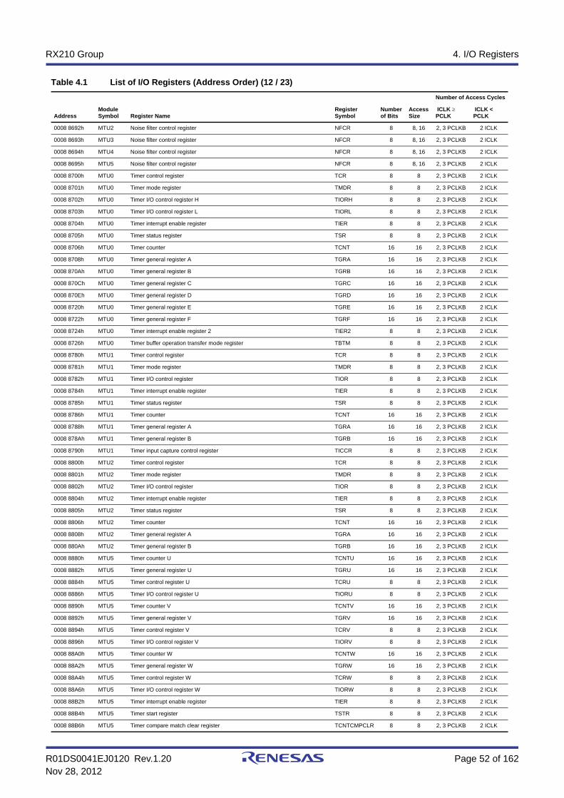
R01DS0041EJ0120 Rev.1.20 Page 52 of 162Nov 28, 2012
RX210 Group 4. I/O Registers
0008 8692h MTU2 Noise filter control register NFCR 8 8, 16 2, 3 PCLKB 2 ICLK
0008 8693h MTU3 Noise filter control register NFCR 8 8, 16 2, 3 PCLKB 2 ICLK
0008 8694h MTU4 Noise filter control register NFCR 8 8, 16 2, 3 PCLKB 2 ICLK
0008 8695h MTU5 Noise filter control register NFCR 8 8, 16 2, 3 PCLKB 2 ICLK
0008 8700h MTU0 Timer control register TCR 8 8 2, 3 PCLKB 2 ICLK
0008 8701h MTU0 Timer mode register TMDR 8 8 2, 3 PCLKB 2 ICLK
0008 8702h MTU0 Timer I/O control register H TIORH 8 8 2, 3 PCLKB 2 ICLK
0008 8703h MTU0 Timer I/O control register L TIORL 8 8 2, 3 PCLKB 2 ICLK
0008 8704h MTU0 Timer interrupt enable register TIER 8 8 2, 3 PCLKB 2 ICLK
0008 8705h MTU0 Timer status register TSR 8 8 2, 3 PCLKB 2 ICLK
0008 8706h MTU0 Timer counter TCNT 16 16 2, 3 PCLKB 2 ICLK
0008 8708h MTU0 Timer general register A TGRA 16 16 2, 3 PCLKB 2 ICLK
0008 870Ah MTU0 Timer general register B TGRB 16 16 2, 3 PCLKB 2 ICLK
0008 870Ch MTU0 Timer general register C TGRC 16 16 2, 3 PCLKB 2 ICLK
0008 870Eh MTU0 Timer general register D TGRD 16 16 2, 3 PCLKB 2 ICLK
0008 8720h MTU0 Timer general register E TGRE 16 16 2, 3 PCLKB 2 ICLK
0008 8722h MTU0 Timer general register F TGRF 16 16 2, 3 PCLKB 2 ICLK
0008 8724h MTU0 Timer interrupt enable register 2 TIER2 8 8 2, 3 PCLKB 2 ICLK
0008 8726h MTU0 Timer buffer operation transfer mode register TBTM 8 8 2, 3 PCLKB 2 ICLK
0008 8780h MTU1 Timer control register TCR 8 8 2, 3 PCLKB 2 ICLK
0008 8781h MTU1 Timer mode register TMDR 8 8 2, 3 PCLKB 2 ICLK
0008 8782h MTU1 Timer I/O control register TIOR 8 8 2, 3 PCLKB 2 ICLK
0008 8784h MTU1 Timer interrupt enable register TIER 8 8 2, 3 PCLKB 2 ICLK
0008 8785h MTU1 Timer status register TSR 8 8 2, 3 PCLKB 2 ICLK
0008 8786h MTU1 Timer counter TCNT 16 16 2, 3 PCLKB 2 ICLK
0008 8788h MTU1 Timer general register A TGRA 16 16 2, 3 PCLKB 2 ICLK
0008 878Ah MTU1 Timer general register B TGRB 16 16 2, 3 PCLKB 2 ICLK
0008 8790h MTU1 Timer input capture control register TICCR 8 8 2, 3 PCLKB 2 ICLK
0008 8800h MTU2 Timer control register TCR 8 8 2, 3 PCLKB 2 ICLK
0008 8801h MTU2 Timer mode register TMDR 8 8 2, 3 PCLKB 2 ICLK
0008 8802h MTU2 Timer I/O control register TIOR 8 8 2, 3 PCLKB 2 ICLK
0008 8804h MTU2 Timer interrupt enable register TIER 8 8 2, 3 PCLKB 2 ICLK
0008 8805h MTU2 Timer status register TSR 8 8 2, 3 PCLKB 2 ICLK
0008 8806h MTU2 Timer counter TCNT 16 16 2, 3 PCLKB 2 ICLK
0008 8808h MTU2 Timer general register A TGRA 16 16 2, 3 PCLKB 2 ICLK
0008 880Ah MTU2 Timer general register B TGRB 16 16 2, 3 PCLKB 2 ICLK
0008 8880h MTU5 Timer counter U TCNTU 16 16 2, 3 PCLKB 2 ICLK
0008 8882h MTU5 Timer general register U TGRU 16 16 2, 3 PCLKB 2 ICLK
0008 8884h MTU5 Timer control register U TCRU 8 8 2, 3 PCLKB 2 ICLK
0008 8886h MTU5 Timer I/O control register U TIORU 8 8 2, 3 PCLKB 2 ICLK
0008 8890h MTU5 Timer counter V TCNTV 16 16 2, 3 PCLKB 2 ICLK
0008 8892h MTU5 Timer general register V TGRV 16 16 2, 3 PCLKB 2 ICLK
0008 8894h MTU5 Timer control register V TCRV 8 8 2, 3 PCLKB 2 ICLK
0008 8896h MTU5 Timer I/O control register V TIORV 8 8 2, 3 PCLKB 2 ICLK
0008 88A0h MTU5 Timer counter W TCNTW 16 16 2, 3 PCLKB 2 ICLK
0008 88A2h MTU5 Timer general register W TGRW 16 16 2, 3 PCLKB 2 ICLK
0008 88A4h MTU5 Timer control register W TCRW 8 8 2, 3 PCLKB 2 ICLK
0008 88A6h MTU5 Timer I/O control register W TIORW 8 8 2, 3 PCLKB 2 ICLK
0008 88B2h MTU5 Timer interrupt enable register TIER 8 8 2, 3 PCLKB 2 ICLK
0008 88B4h MTU5 Timer start register TSTR 8 8 2, 3 PCLKB 2 ICLK
0008 88B6h MTU5 Timer compare match clear register TCNTCMPCLR 8 8 2, 3 PCLKB 2 ICLK
Table 4.1 List of I/O Registers (Address Order) (12 / 23)
AddressModule Symbol Register Name
Register Symbol
Number of Bits
Access Size
Number of Access Cycles
ICLK PCLK
ICLK <PCLK

R01DS0041EJ0120 Rev.1.20 Page 53 of 162Nov 28, 2012
RX210 Group 4. I/O Registers
0008 8900h POE Input level control/status register 1 ICSR1 16 8, 16 2, 3 PCLKB 2 ICLK
0008 8902h POE Output level control/status register 1 OCSR1 16 8, 16 2, 3 PCLKB 2 ICLK
0008 8908h POE Input level control/status register 2 ICSR2 16 8, 16 2, 3 PCLKB 2 ICLK
0008 890Ah POE Software port output enable register SPOER 8 8 2, 3 PCLKB 2 ICLK
0008 890Bh POE Port output enable control register 1 POECR1 8 8 2, 3 PCLKB 2 ICLK
0008 890Ch POE Port output enable control register 2 POECR2 8 8 2, 3 PCLKB 2 ICLK
0008 890Eh POE Input level control/status register 3 ICSR3 16 8, 16 2, 3 PCLKB 2 ICLK
0008 9000h S12AD A/D control register ADCSR 16 16 2, 3 PCLKB 2 ICLK
0008 9004h S12AD A/D channel select register A ADANSA 16 16 2, 3 PCLKB 2 ICLK
0008 9008h S12AD A/D-converted value addition mode select register ADADS 16 16 2, 3 PCLKB 2 ICLK
0008 900Ch S12AD A/D-converted value addition count select register ADADC 8 8 2, 3 PCLKB 2 ICLK
0008 900Eh S12AD A/D control extended register ADCER 16 16 2, 3 PCLKB 2 ICLK
0008 9010h S12AD A/D start trigger select register ADSTRGR 16 16 2, 3 PCLKB 2 ICLK
0008 9012h S12AD A/D converted extended input control register ADEXICR 16 16 2, 3 PCLKB 2 ICLK
0008 9014h S12AD A/D channel select register B ADANSB 16 16 2, 3 PCLKB 2 ICLK
0008 9018h S12AD A/D double register ADDBLDR 16 16 2, 3 PCLKB 2 ICLK
0008 901Ah S12AD A/D temperature sensor data register ADTSDR 16 16 2, 3 PCLKB 2 ICLK
0008 901Ch S12AD A/D internal reference voltage data register ADOCDR 16 16 2, 3 PCLKB 2 ICLK
0008 901Eh S12AD A/D self-diagnosis data register ADRD 16 16 2, 3 PCLKB 2 ICLK
0008 9020h S12AD A/D data register 0 ADDR0 16 16 2, 3 PCLKB 2 ICLK
0008 9022h S12AD A/D data register 1 ADDR1 16 16 2, 3 PCLKB 2 ICLK
0008 9024h S12AD A/D data register 2 ADDR2 16 16 2, 3 PCLKB 2 ICLK
0008 9026h S12AD A/D data register 3 ADDR3 16 16 2, 3 PCLKB 2 ICLK
0008 9028h S12AD A/D data register 4 ADDR4 16 16 2, 3 PCLKB 2 ICLK
0008 902Ah S12AD A/D data register 5 ADDR5 16 16 2, 3 PCLKB 2 ICLK
0008 902Ch S12AD A/D data register 6 ADDR6 16 16 2, 3 PCLKB 2 ICLK
0008 902Eh S12AD A/D data register 7 ADDR7 16 16 2, 3 PCLKB 2 ICLK
0008 9030h S12AD A/D data register 8 ADDR8 16 16 2, 3 PCLKB 2 ICLK
0008 9032h S12AD A/D data register 9 ADDR9 16 16 2, 3 PCLKB 2 ICLK
0008 9034h S12AD A/D data register 10 ADDR10 16 16 2, 3 PCLKB 2 ICLK
0008 9036h S12AD A/D data register 11 ADDR11 16 16 2, 3 PCLKB 2 ICLK
0008 9038h S12AD A/D data register 12 ADDR12 16 16 2, 3 PCLKB 2 ICLK
0008 903Ah S12AD A/D data register 13 ADDR13 16 16 2, 3 PCLKB 2 ICLK
0008 903Ch S12AD A/D data register 14 ADDR14 16 16 2, 3 PCLKB 2 ICLK
0008 903Eh S12AD A/D data register 15 ADDR15 16 16 2, 3 PCLKB 2 ICLK
0008 9060h S12AD A/D sampling state register 0 ADSSTR0 8 8 2, 3 PCLKB 2 ICLK
0008 9061h S12AD A/D sampling state register L ADSSTRL 8 8 2, 3 PCLKB 2 ICLK
0008 9066h S12AD A/D sample and hold circuit register ADSHCR 16 16 2, 3 PCLKB 2 ICLK
0008 9070h S12AD A/D sampling state register T ADSSTRT 8 8 2, 3 PCLKB 2 ICLK
0008 9071h S12AD A/D sampling state register O ADSSTRO 8 8 2, 3 PCLKB 2 ICLK
0008 9073h S12AD A/D sampling state register 1 ADSSTR1 8 8 2, 3 PCLKB 2 ICLK
0008 9074h S12AD A/D sampling state register 2 ADSSTR2 8 8 2, 3 PCLKB 2 ICLK
0008 9075h S12AD A/D sampling state register 3 ADSSTR3 8 8 2, 3 PCLKB 2 ICLK
0008 9076h S12AD A/D sampling state register 4 ADSSTR4 8 8 2, 3 PCLKB 2 ICLK
0008 9077h S12AD A/D sampling state register 5 ADSSTR5 8 8 2, 3 PCLKB 2 ICLK
0008 9078h S12AD A/D sampling state register 6 ADSSTR6 8 8 2, 3 PCLKB 2 ICLK
0008 9079h S12AD A/D sampling state register 7 ADSSTR7 8 8 2, 3 PCLKB 2 ICLK
0008 907Ah S12AD A/D disconnecting detection control register ADDISCR 8 8 2, 3 PCLKB 2 ICLK
0008 A000h SCI0 Serial mode register SMR 8 8 2, 3 PCLKB 2 ICLK
0008 A001h SCI0 Bit rate register BRR 8 8 2, 3 PCLKB 2 ICLK
0008 A002h SCI0 Serial control register SCR 8 8 2, 3 PCLKB 2 ICLK
Table 4.1 List of I/O Registers (Address Order) (13 / 23)
AddressModule Symbol Register Name
Register Symbol
Number of Bits
Access Size
Number of Access Cycles
ICLK PCLK
ICLK <PCLK
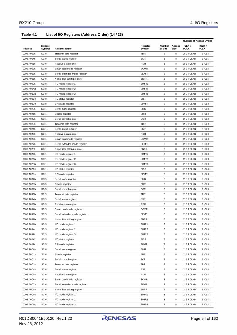
R01DS0041EJ0120 Rev.1.20 Page 54 of 162Nov 28, 2012
RX210 Group 4. I/O Registers
0008 A003h SCI0 Transmit data register TDR 8 8 2, 3 PCLKB 2 ICLK
0008 A004h SCI0 Serial status register SSR 8 8 2, 3 PCLKB 2 ICLK
0008 A005h SCI0 Receive data register RDR 8 8 2, 3 PCLKB 2 ICLK
0008 A006h SCI0 Smart card mode register SCMR 8 8 2, 3 PCLKB 2 ICLK
0008 A007h SCI0 Serial extended mode register SEMR 8 8 2, 3 PCLKB 2 ICLK
0008 A008h SCI0 Noise filter setting register SNFR 8 8 2, 3 PCLKB 2 ICLK
0008 A009h SCI0 I2C mode register 1 SIMR1 8 8 2, 3 PCLKB 2 ICLK
0008 A00Ah SCI0 I2C mode register 2 SIMR2 8 8 2, 3 PCLKB 2 ICLK
0008 A00Bh SCI0 I2C mode register 3 SIMR3 8 8 2, 3 PCLKB 2 ICLK
0008 A00Ch SCI0 I2C status register SISR 8 8 2, 3 PCLKB 2 ICLK
0008 A00Dh SCI0 SPI mode register SPMR 8 8 2, 3 PCLKB 2 ICLK
0008 A020h SCI1 Serial mode register SMR 8 8 2, 3 PCLKB 2 ICLK
0008 A021h SCI1 Bit rate register BRR 8 8 2, 3 PCLKB 2 ICLK
0008 A022h SCI1 Serial control register SCR 8 8 2, 3 PCLKB 2 ICLK
0008 A023h SCI1 Transmit data register TDR 8 8 2, 3 PCLKB 2 ICLK
0008 A024h SCI1 Serial status register SSR 8 8 2, 3 PCLKB 2 ICLK
0008 A025h SCI1 Receive data register RDR 8 8 2, 3 PCLKB 2 ICLK
0008 A026h SCI1 Smart card mode register SCMR 8 8 2, 3 PCLKB 2 ICLK
0008 A027h SCI1 Serial extended mode register SEMR 8 8 2, 3 PCLKB 2 ICLK
0008 A028h SCI1 Noise filter setting register SNFR 8 8 2, 3 PCLKB 2 ICLK
0008 A029h SCI1 I2C mode register 1 SIMR1 8 8 2, 3 PCLKB 2 ICLK
0008 A02Ah SCI1 I2C mode register 2 SIMR2 8 8 2, 3 PCLKB 2 ICLK
0008 A02Bh SCI1 I2C mode register 3 SIMR3 8 8 2, 3 PCLKB 2 ICLK
0008 A02Ch SCI1 I2C status register SISR 8 8 2, 3 PCLKB 2 ICLK
0008 A02Dh SCI1 SPI mode register SPMR 8 8 2, 3 PCLKB 2 ICLK
0008 A0A0h SCI5 Serial mode register SMR 8 8 2, 3 PCLKB 2 ICLK
0008 A0A1h SCI5 Bit rate register BRR 8 8 2, 3 PCLKB 2 ICLK
0008 A0A2h SCI5 Serial control register SCR 8 8 2, 3 PCLKB 2 ICLK
0008 A0A3h SCI5 Transmit data register TDR 8 8 2, 3 PCLKB 2 ICLK
0008 A0A4h SCI5 Serial status register SSR 8 8 2, 3 PCLKB 2 ICLK
0008 A0A5h SCI5 Receive data register RDR 8 8 2, 3 PCLKB 2 ICLK
0008 A0A6h SCI5 Smart card mode register SCMR 8 8 2, 3 PCLKB 2 ICLK
0008 A0A7h SCI5 Serial extended mode register SEMR 8 8 2, 3 PCLKB 2 ICLK
0008 A0A8h SCI5 Noise filter setting register SNFR 8 8 2, 3 PCLKB 2 ICLK
0008 A0A9h SCI5 I2C mode register 1 SIMR1 8 8 2, 3 PCLKB 2 ICLK
0008 A0AAh SCI5 I2C mode register 2 SIMR2 8 8 2, 3 PCLKB 2 ICLK
0008 A0ABh SCI5 I2C mode register 3 SIMR3 8 8 2, 3 PCLKB 2 ICLK
0008 A0ACh SCI5 I2C status register SISR 8 8 2, 3 PCLKB 2 ICLK
0008 A0ADh SCI5 SPI mode register SPMR 8 8 2, 3 PCLKB 2 ICLK
0008 A0C0h SCI6 Serial mode register SMR 8 8 2, 3 PCLKB 2 ICLK
0008 A0C1h SCI6 Bit rate register BRR 8 8 2, 3 PCLKB 2 ICLK
0008 A0C2h SCI6 Serial control register SCR 8 8 2, 3 PCLKB 2 ICLK
0008 A0C3h SCI6 Transmit data register TDR 8 8 2, 3 PCLKB 2 ICLK
0008 A0C4h SCI6 Serial status register SSR 8 8 2, 3 PCLKB 2 ICLK
0008 A0C5h SCI6 Receive data register RDR 8 8 2, 3 PCLKB 2 ICLK
0008 A0C6h SCI6 Smart card mode register SCMR 8 8 2, 3 PCLKB 2 ICLK
0008 A0C7h SCI6 Serial extended mode register SEMR 8 8 2, 3 PCLKB 2 ICLK
0008 A0C8h SCI6 Noise filter setting register SNFR 8 8 2, 3 PCLKB 2 ICLK
0008 A0C9h SCI6 I2C mode register 1 SIMR1 8 8 2, 3 PCLKB 2 ICLK
0008 A0CAh SCI6 I2C mode register 2 SIMR2 8 8 2, 3 PCLKB 2 ICLK
0008 A0CBh SCI6 I2C mode register 3 SIMR3 8 8 2, 3 PCLKB 2 ICLK
Table 4.1 List of I/O Registers (Address Order) (14 / 23)
AddressModule Symbol Register Name
Register Symbol
Number of Bits
Access Size
Number of Access Cycles
ICLK PCLK
ICLK <PCLK

R01DS0041EJ0120 Rev.1.20 Page 55 of 162Nov 28, 2012
RX210 Group 4. I/O Registers
0008 A0CCh SCI6 I2C status register SISR 8 8 2, 3 PCLKB 2 ICLK
0008 A0CDh SCI6 SPI mode register SPMR 8 8 2, 3 PCLKB 2 ICLK
0008 A100h SCI8 Serial mode register SMR 8 8 2, 3 PCLKB 2 ICLK
0008 A101h SCI8 Bit rate register BRR 8 8 2, 3 PCLKB 2 ICLK
0008 A102h SCI8 Serial control register SCR 8 8 2, 3 PCLKB 2 ICLK
0008 A103h SCI8 Transmit data register TDR 8 8 2, 3 PCLKB 2 ICLK
0008 A104h SCI8 Serial status register SSR 8 8 2, 3 PCLKB 2 ICLK
0008 A105h SCI8 Receive data register RDR 8 8 2, 3 PCLKB 2 ICLK
0008 A106h SCI8 Smart card mode register SCMR 8 8 2, 3 PCLKB 2 ICLK
0008 A107h SCI8 Serial extended mode register SEMR 8 8 2, 3 PCLKB 2 ICLK
0008 A108h SCI8 Noise filter setting register SNFR 8 8 2, 3 PCLKB 2 ICLK
0008 A109h SCI8 I2C mode register 1 SIMR1 8 8 2, 3 PCLKB 2 ICLK
0008 A10Ah SCI8 I2C mode register 2 SIMR2 8 8 2, 3 PCLKB 2 ICLK
0008 A10Bh SCI8 I2C mode register 3 SIMR3 8 8 2, 3 PCLKB 2 ICLK
0008 A10Ch SCI8 I2C status register SISR 8 8 2, 3 PCLKB 2 ICLK
0008 A10Dh SCI8 SPI mode register SPMR 8 8 2, 3 PCLKB 2 ICLK
0008 A120h SCI9 Serial mode register SMR 8 8 2, 3 PCLKB 2 ICLK
0008 A121h SCI9 Bit rate register BRR 8 8 2, 3 PCLKB 2 ICLK
0008 A122h SCI9 Serial control register SCR 8 8 2, 3 PCLKB 2 ICLK
0008 A123h SCI9 Transmit data register TDR 8 8 2, 3 PCLKB 2 ICLK
0008 A124h SCI9 Serial status register SSR 8 8 2, 3 PCLKB 2 ICLK
0008 A125h SCI9 Receive data register RDR 8 8 2, 3 PCLKB 2 ICLK
0008 A126h SCI9 Smart card mode register SCMR 8 8 2, 3 PCLKB 2 ICLK
0008 A127h SCI9 Serial extended mode register SEMR 8 8 2, 3 PCLKB 2 ICLK
0008 A128h SCI9 Noise filter setting register SNFR 8 8 2, 3 PCLKB 2 ICLK
0008 A129h SCI9 I2C mode register 1 SIMR1 8 8 2, 3 PCLKB 2 ICLK
0008 A12Ah SCI9 I2C mode register 2 SIMR2 8 8 2, 3 PCLKB 2 ICLK
0008 A12Bh SCI9 I2C mode register 3 SIMR3 8 8 2, 3 PCLKB 2 ICLK
0008 A12Ch SCI9 I2C status register SISR 8 8 2, 3 PCLKB 2 ICLK
0008 A12Dh SCI9 SPI mode register SPMR 8 8 2, 3 PCLKB 2 ICLK
0008 B000h CAC CAC control register 0 CACR0 8 8 2, 3 PCLKB 2 ICLK
0008 B001h CAC CAC control register 1 CACR1 8 8 2, 3 PCLKB 2 ICLK
0008 B002h CAC CAC control register 2 CACR2 8 8 2, 3 PCLKB 2 ICLK
0008 B003h CAC CAC interrupt control register CAICR 8 8 2, 3 PCLKB 2 ICLK
0008 B004h CAC CAC status register CASTR 8 8 2, 3 PCLKB 2 ICLK
0008 B006h CAC CAC upper-limit value setting register CAULVR 16 16 2, 3 PCLKB 2 ICLK
0008 B008h CAC CAC lower-limit value setting register CALLVR 16 16 2, 3 PCLKB 2 ICLK
0008 B00Ah CAC CAC counter buffer register CACNTBR 16 16 2, 3 PCLKB 2 ICLK
0008 B080h DOC DOC control register DOCR 8 8 2, 3 PCLKB 2 ICLK
0008 B082h DOC DOC data input register DODIR 16 16 2, 3 PCLKB 2 ICLK
0008 B084h DOC DOC data setting register DODSR 16 16 2, 3 PCLKB 2 ICLK
0008 B100h ELC Event link control register ELCR 8 8 2, 3 PCLKB 2 ICLK
0008 B102h ELC Event link setting register 1 ELSR1 8 8 2, 3 PCLKB 2 ICLK
0008 B103h ELC Event link setting register 2 ELSR2 8 8 2, 3 PCLKB 2 ICLK
0008 B104h ELC Event link setting register 3 ELSR3 8 8 2, 3 PCLKB 2 ICLK
0008 B105h ELC Event link setting register 4 ELSR4 8 8 2, 3 PCLKB 2 ICLK
0008 B108h ELC Event link setting register 7 ELSR7 8 8 2, 3 PCLKB 2 ICLK
0008 B10Bh ELC Event link setting register 10 ELSR10 8 8 2, 3 PCLKB 2 ICLK
0008 B10Dh ELC Event link setting register 12 ELSR12 8 8 2, 3 PCLKB 2 ICLK
0008 B110h ELC Event link setting register 15 ELSR15 8 8 2, 3 PCLKB 2 ICLK
0008 B111h ELC Event link setting register 16 ELSR16 8 8 2, 3 PCLKB 2 ICLK
Table 4.1 List of I/O Registers (Address Order) (15 / 23)
AddressModule Symbol Register Name
Register Symbol
Number of Bits
Access Size
Number of Access Cycles
ICLK PCLK
ICLK <PCLK

R01DS0041EJ0120 Rev.1.20 Page 56 of 162Nov 28, 2012
RX210 Group 4. I/O Registers
0008 B113h ELC Event link setting register 18 ELSR18 8 8 2, 3 PCLKB 2 ICLK
0008 B114h ELC Event link setting register 19 ELSR19 8 8 2, 3 PCLKB 2 ICLK
0008 B115h ELC Event link setting register 20 ELSR20 8 8 2, 3 PCLKB 2 ICLK
0008 B116h ELC Event link setting register 21 ELSR21 8 8 2, 3 PCLKB 2 ICLK
0008 B117h ELC Event link setting register 22 ELSR22 8 8 2, 3 PCLKB 2 ICLK
0008 B118h ELC Event link setting register 23 ELSR23 8 8 2, 3 PCLKB 2 ICLK
0008 B119h ELC Event link setting register 24 ELSR24 8 8 2, 3 PCLKB 2 ICLK
0008 B11Ah ELC Event link setting register 25 ELSR25 8 8 2, 3 PCLKB 2 ICLK
0008 B11Bh ELC Event link setting register 26 ELSR26 8 8 2, 3 PCLKB 2 ICLK
0008 B11Ch ELC Event link setting register 27 ELSR27 8 8 2, 3 PCLKB 2 ICLK
0008 B11Dh ELC Event link setting register 28 ELSR28 8 8 2, 3 PCLKB 2 ICLK
0008 B11Eh ELC Event link setting register 29 ELSR29 8 8 2, 3 PCLKB 2 ICLK
0008 B11Fh ELC Event link option setting register A ELOPA 8 8 2, 3 PCLKB 2 ICLK
0008 B120h ELC Event link option setting register B ELOPB 8 8 2, 3 PCLKB 2 ICLK
0008 B121h ELC Event link option setting register C ELOPC 8 8 2, 3 PCLKB 2 ICLK
0008 B122h ELC Event link option setting register D ELOPD 8 8 2, 3 PCLKB 2 ICLK
0008 B123h ELC Port group setting register 1 PGR1 8 8 2, 3 PCLKB 2 ICLK
0008 B124h ELC Port group setting register 2 PGR2 8 8 2, 3 PCLKB 2 ICLK
0008 B125h ELC Port group control register 1 PGC1 8 8 2, 3 PCLKB 2 ICLK
0008 B126h ELC Port group control register 2 PGC2 8 8 2, 3 PCLKB 2 ICLK
0008 B127h ELC Port buffer register 1 PDBF1 8 8 2, 3 PCLKB 2 ICLK
0008 B128h ELC Port buffer register 2 PDBF2 8 8 2, 3 PCLKB 2 ICLK
0008 B129h ELC Event link port setting register 0 PEL0 8 8 2, 3 PCLKB 2 ICLK
0008 B12Ah ELC Event link port setting register 1 PEL1 8 8 2, 3 PCLKB 2 ICLK
0008 B12Bh ELC Event link port setting register 2 PEL2 8 8 2, 3 PCLKB 2 ICLK
0008 B12Ch ELC Event link port setting register 3 PEL3 8 8 2, 3 PCLKB 2 ICLK
0008 B12Dh ELC Event link software event generation register ELSEGR 8 8 2, 3 PCLKB 2 ICLK
0008 B300h SCI12 Serial mode register SMR 8 8 2, 3 PCLKB 2 ICLK
0008 B301h SCI12 Bit rate register BRR 8 8 2, 3 PCLKB 2 ICLK
0008 B302h SCI12 Serial control register SCR 8 8 2, 3 PCLKB 2 ICLK
0008 B303h SCI12 Transmit data register TDR 8 8 2, 3 PCLKB 2 ICLK
0008 B304h SCI12 Serial status register SSR 8 8 2, 3 PCLKB 2 ICLK
0008 B305h SCI12 Receive data register RDR 8 8 2, 3 PCLKB 2 ICLK
0008 B306h SCI12 Smart card mode register SCMR 8 8 2, 3 PCLKB 2 ICLK
0008 B307h SCI12 Serial extended mode register SEMR 8 8 2, 3 PCLKB 2 ICLK
0008 B308h SCI12 Noise filter setting register SNFR 8 8 2, 3 PCLKB 2 ICLK
0008 B309h SCI12 I2C mode register 1 SIMR1 8 8 2, 3 PCLKB 2 ICLK
0008 B30Ah SCI12 I2C mode register 2 SIMR2 8 8 2, 3 PCLKB 2 ICLK
0008 B30Bh SCI12 I2C mode register 3 SIMR3 8 8 2, 3 PCLKB 2 ICLK
0008 B30Ch SCI12 I2C status register SISR 8 8 2, 3 PCLKB 2 ICLK
0008 B30Dh SCI12 SPI mode register SPMR 8 8 2, 3 PCLKB 2 ICLK
0008 B320h SCI12 Extended serial mode enable register ESMER 8 8 2, 3 PCLKB 2 ICLK
0008 B321h SCI12 Control register 0 CR0 8 8 2, 3 PCLKB 2 ICLK
0008 B322h SCI12 Control register 1 CR1 8 8 2, 3 PCLKB 2 ICLK
0008 B323h SCI12 Control register 2 CR2 8 8 2, 3 PCLKB 2 ICLK
0008 B324h SCI12 Control register 3 CR3 8 8 2, 3 PCLKB 2 ICLK
0008 B325h SCI12 Port control register PCR 8 8 2, 3 PCLKB 2 ICLK
0008 B326h SCI12 Interrupt control register ICR 8 8 2, 3 PCLKB 2 ICLK
0008 B327h SCI12 Status register STR 8 8 2, 3 PCLKB 2 ICLK
0008 B328h SCI12 Status clear register STCR 8 8 2, 3 PCLKB 2 ICLK
0008 B329h SCI12 Control Field 0 data register CF0DR 8 8 2, 3 PCLKB 2 ICLK
Table 4.1 List of I/O Registers (Address Order) (16 / 23)
AddressModule Symbol Register Name
Register Symbol
Number of Bits
Access Size
Number of Access Cycles
ICLK PCLK
ICLK <PCLK

R01DS0041EJ0120 Rev.1.20 Page 57 of 162Nov 28, 2012
RX210 Group 4. I/O Registers
0008 B32Ah SCI12 Control Field 0 compare enable register CF0CR 8 8 2, 3 PCLKB 2 ICLK
0008 B32Bh SCI12 Control Field 0 receive data register CF0RR 8 8 2, 3 PCLKB 2 ICLK
0008 B32Ch SCI12 Primary control field 1 data register PCF1DR 8 8 2, 3 PCLKB 2 ICLK
0008 B32Dh SCI12 Secondary control field 1 data register SCF1DR 8 8 2, 3 PCLKB 2 ICLK
0008 B32Eh SCI12 Control field 1 compare enable register CF1CR 8 8 2, 3 PCLKB 2 ICLK
0008 B32Fh SCI12 Control field 1 receive data register CF1RR 8 8 2, 3 PCLKB 2 ICLK
0008 B330h SCI12 Timer control register TCR 8 8 2, 3 PCLKB 2 ICLK
0008 B331h SCI12 Timer mode register TMR 8 8 2, 3 PCLKB 2 ICLK
0008 B332h SCI12 Timer prescaler register TPRE 8 8 2, 3 PCLKB 2 ICLK
0008 B333h SCI12 Timer count register TCNT 8 8 2, 3 PCLKB 2 ICLK
0008 C000h PORT0 Port direction register PDR 8 8 2, 3 PCLKB 2 ICLK
0008 C001h PORT1 Port direction register PDR 8 8 2, 3 PCLKB 2 ICLK
0008 C002h PORT2 Port direction register PDR 8 8 2, 3 PCLKB 2 ICLK
0008 C003h PORT3 Port direction register PDR 8 8 2, 3 PCLKB 2 ICLK
0008 C004h PORT4 Port direction register PDR 8 8 2, 3 PCLKB 2 ICLK
0008 C005h PORT5 Port direction register PDR 8 8 2, 3 PCLKB 2 ICLK
0008 C00Ah PORTA Port direction register PDR 8 8 2, 3 PCLKB 2 ICLK
0008 C00Bh PORTB Port direction register PDR 8 8 2, 3 PCLKB 2 ICLK
0008 C00Ch PORTC Port direction register PDR 8 8 2, 3 PCLKB 2 ICLK
0008 C00Dh PORTD Port direction register PDR 8 8 2, 3 PCLKB 2 ICLK
0008 C00Eh PORTE Port direction register PDR 8 8 2, 3 PCLKB 2 ICLK
0008 C011h PORTH Port direction register PDR 8 8 2, 3 PCLKB 2 ICLK
0008 C012h PORTJ Port direction register PDR 8 8 2, 3 PCLKB 2 ICLK
0008 C020h PORT0 Port output data register PODR 8 8 2, 3 PCLKB 2 ICLK
0008 C021h PORT1 Port output data register PODR 8 8 2, 3 PCLKB 2 ICLK
0008 C022h PORT2 Port output data register PODR 8 8 2, 3 PCLKB 2 ICLK
0008 C023h PORT3 Port output data register PODR 8 8 2, 3 PCLKB 2 ICLK
0008 C024h PORT4 Port output data register PODR 8 8 2, 3 PCLKB 2 ICLK
0008 C025h PORT5 Port output data register PODR 8 8 2, 3 PCLKB 2 ICLK
0008 C02Ah PORTA Port output data register PODR 8 8 2, 3 PCLKB 2 ICLK
0008 C02Bh PORTB Port output data register PODR 8 8 2, 3 PCLKB 2 ICLK
0008 C02Ch PORTC Port output data register PODR 8 8 2, 3 PCLKB 2 ICLK
0008 C02Dh PORTD Port output data register PODR 8 8 2, 3 PCLKB 2 ICLK
0008 C02Eh PORTE Port output data register PODR 8 8 2, 3 PCLKB 2 ICLK
0008 C031h PORTH Port output data register PODR 8 8 2, 3 PCLKB 2 ICLK
0008 C032h PORTJ Port output data register PODR 8 8 2, 3 PCLKB 2 ICLK
0008 C040h PORT0 Port input data register PIDR 8 8 3 or 4 PCLKB
cycles when reading, 2 or 3
PCLKB cycles when
writing
3 ICLK cycles when
reading, 2 ICLK
cycles when writing
0008 C041h PORT1 Port input data register PIDR 8 8 3 or 4 PCLKB
cycles when reading, 2 or 3
PCLKB cycles when
writing
3 ICLK cycles when
reading, 2 ICLK
cycles when writing
0008 C042h PORT2 Port input data register PIDR 8 8 3 or 4 PCLKB
cycles when reading, 2 or 3
PCLKB cycles when
writing
3 ICLK cycles when
reading, 2 ICLK
cycles when writing
Table 4.1 List of I/O Registers (Address Order) (17 / 23)
AddressModule Symbol Register Name
Register Symbol
Number of Bits
Access Size
Number of Access Cycles
ICLK PCLK
ICLK <PCLK

R01DS0041EJ0120 Rev.1.20 Page 58 of 162Nov 28, 2012
RX210 Group 4. I/O Registers
0008 C043h PORT3 Port input data register PIDR 8 8 3 or 4 PCLKB
cycles when reading, 2 or 3
PCLKB cycles when
writing
3 ICLK cycles when
reading, 2 ICLK
cycles when writing
0008 C044h PORT4 Port input data register PIDR 8 8 3 or 4 PCLKB
cycles when reading, 2 or 3
PCLKB cycles when
writing
3 ICLK cycles when
reading, 2 ICLK
cycles when writing
0008 C045h PORT5 Port input data register PIDR 8 8 3 or 4 PCLKB
cycles when reading, 2 or 3
PCLKB cycles when
writing
3 ICLK cycles when
reading, 2 ICLK
cycles when writing
0008 C04Ah PORTA Port input data register PIDR 8 8 3 or 4 PCLKB
cycles when reading, 2 or 3
PCLKB cycles when
writing
3 ICLK cycles when
reading, 2 ICLK
cycles when writing
0008 C04Bh PORTB Port input data register PIDR 8 8 3 or 4 PCLKB
cycles when reading, 2 or 3
PCLKB cycles when
writing
3 ICLK cycles when
reading, 2 ICLK
cycles when writing
0008 C04Ch PORTC Port input data register PIDR 8 8 3 or 4 PCLKB
cycles when reading, 2 or 3
PCLKB cycles when
writing
3 ICLK cycles when
reading, 2 ICLK
cycles when writing
0008 C04Dh PORTD Port input data register PIDR 8 8 3 or 4 PCLKB
cycles when reading, 2 or 3
PCLKB cycles when
writing
3 ICLK cycles when
reading, 2 ICLK
cycles when writing
0008 C04Eh PORTE Port input data register PIDR 8 8 3 or 4 PCLKB
cycles when reading, 2 or 3
PCLKB cycles when
writing
3 ICLK cycles when
reading, 2 ICLK
cycles when writing
0008 C051h PORTH Port input data register PIDR 8 8 3 or 4 PCLKB
cycles when reading, 2 or 3
PCLKB cycles when
writing
3 ICLK cycles when
reading, 2 ICLK
cycles when writing
0008 C052h PORTJ Port input data register PIDR 8 8 3 or 4 PCLKB
cycles when reading, 2 or 3
PCLKB cycles when
writing
3 ICLK cycles when
reading, 2 ICLK
cycles when writing
0008 C060h PORT0 Port mode register PMR 8 8 2, 3 PCLKB 2 ICLK
0008 C061h PORT1 Port mode register PMR 8 8 2, 3 PCLKB 2 ICLK
Table 4.1 List of I/O Registers (Address Order) (18 / 23)
AddressModule Symbol Register Name
Register Symbol
Number of Bits
Access Size
Number of Access Cycles
ICLK PCLK
ICLK <PCLK
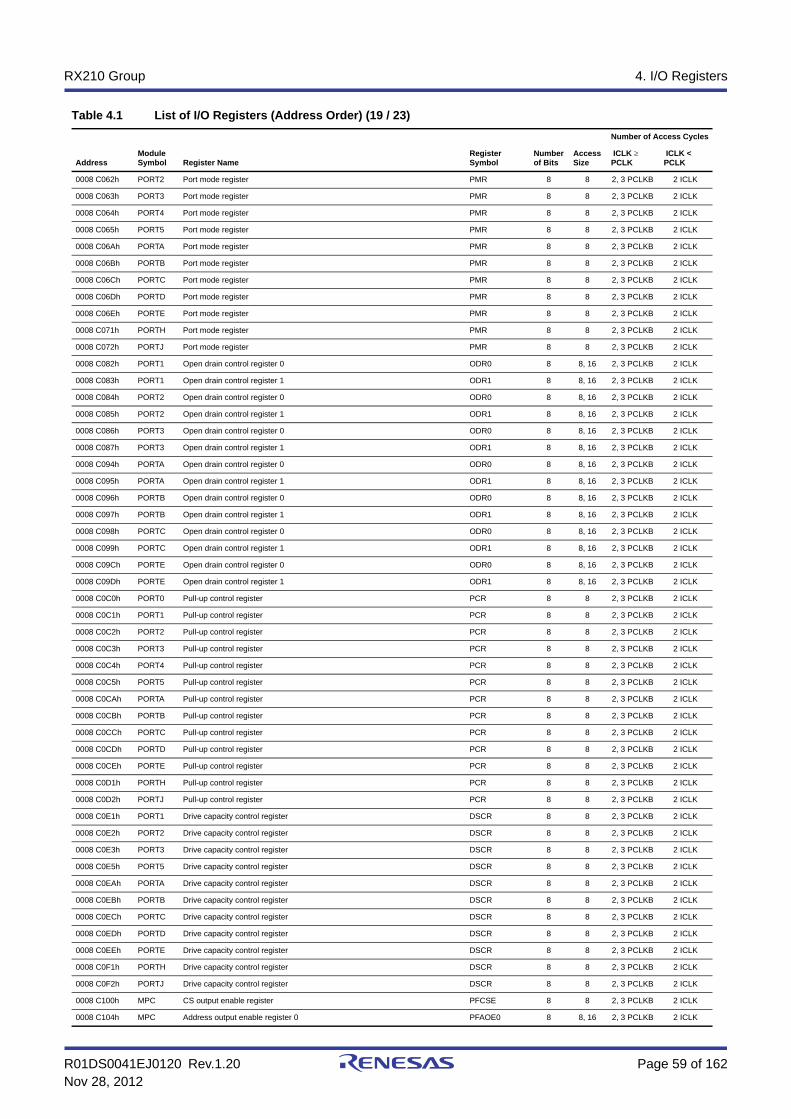
R01DS0041EJ0120 Rev.1.20 Page 59 of 162Nov 28, 2012
RX210 Group 4. I/O Registers
0008 C062h PORT2 Port mode register PMR 8 8 2, 3 PCLKB 2 ICLK
0008 C063h PORT3 Port mode register PMR 8 8 2, 3 PCLKB 2 ICLK
0008 C064h PORT4 Port mode register PMR 8 8 2, 3 PCLKB 2 ICLK
0008 C065h PORT5 Port mode register PMR 8 8 2, 3 PCLKB 2 ICLK
0008 C06Ah PORTA Port mode register PMR 8 8 2, 3 PCLKB 2 ICLK
0008 C06Bh PORTB Port mode register PMR 8 8 2, 3 PCLKB 2 ICLK
0008 C06Ch PORTC Port mode register PMR 8 8 2, 3 PCLKB 2 ICLK
0008 C06Dh PORTD Port mode register PMR 8 8 2, 3 PCLKB 2 ICLK
0008 C06Eh PORTE Port mode register PMR 8 8 2, 3 PCLKB 2 ICLK
0008 C071h PORTH Port mode register PMR 8 8 2, 3 PCLKB 2 ICLK
0008 C072h PORTJ Port mode register PMR 8 8 2, 3 PCLKB 2 ICLK
0008 C082h PORT1 Open drain control register 0 ODR0 8 8, 16 2, 3 PCLKB 2 ICLK
0008 C083h PORT1 Open drain control register 1 ODR1 8 8, 16 2, 3 PCLKB 2 ICLK
0008 C084h PORT2 Open drain control register 0 ODR0 8 8, 16 2, 3 PCLKB 2 ICLK
0008 C085h PORT2 Open drain control register 1 ODR1 8 8, 16 2, 3 PCLKB 2 ICLK
0008 C086h PORT3 Open drain control register 0 ODR0 8 8, 16 2, 3 PCLKB 2 ICLK
0008 C087h PORT3 Open drain control register 1 ODR1 8 8, 16 2, 3 PCLKB 2 ICLK
0008 C094h PORTA Open drain control register 0 ODR0 8 8, 16 2, 3 PCLKB 2 ICLK
0008 C095h PORTA Open drain control register 1 ODR1 8 8, 16 2, 3 PCLKB 2 ICLK
0008 C096h PORTB Open drain control register 0 ODR0 8 8, 16 2, 3 PCLKB 2 ICLK
0008 C097h PORTB Open drain control register 1 ODR1 8 8, 16 2, 3 PCLKB 2 ICLK
0008 C098h PORTC Open drain control register 0 ODR0 8 8, 16 2, 3 PCLKB 2 ICLK
0008 C099h PORTC Open drain control register 1 ODR1 8 8, 16 2, 3 PCLKB 2 ICLK
0008 C09Ch PORTE Open drain control register 0 ODR0 8 8, 16 2, 3 PCLKB 2 ICLK
0008 C09Dh PORTE Open drain control register 1 ODR1 8 8, 16 2, 3 PCLKB 2 ICLK
0008 C0C0h PORT0 Pull-up control register PCR 8 8 2, 3 PCLKB 2 ICLK
0008 C0C1h PORT1 Pull-up control register PCR 8 8 2, 3 PCLKB 2 ICLK
0008 C0C2h PORT2 Pull-up control register PCR 8 8 2, 3 PCLKB 2 ICLK
0008 C0C3h PORT3 Pull-up control register PCR 8 8 2, 3 PCLKB 2 ICLK
0008 C0C4h PORT4 Pull-up control register PCR 8 8 2, 3 PCLKB 2 ICLK
0008 C0C5h PORT5 Pull-up control register PCR 8 8 2, 3 PCLKB 2 ICLK
0008 C0CAh PORTA Pull-up control register PCR 8 8 2, 3 PCLKB 2 ICLK
0008 C0CBh PORTB Pull-up control register PCR 8 8 2, 3 PCLKB 2 ICLK
0008 C0CCh PORTC Pull-up control register PCR 8 8 2, 3 PCLKB 2 ICLK
0008 C0CDh PORTD Pull-up control register PCR 8 8 2, 3 PCLKB 2 ICLK
0008 C0CEh PORTE Pull-up control register PCR 8 8 2, 3 PCLKB 2 ICLK
0008 C0D1h PORTH Pull-up control register PCR 8 8 2, 3 PCLKB 2 ICLK
0008 C0D2h PORTJ Pull-up control register PCR 8 8 2, 3 PCLKB 2 ICLK
0008 C0E1h PORT1 Drive capacity control register DSCR 8 8 2, 3 PCLKB 2 ICLK
0008 C0E2h PORT2 Drive capacity control register DSCR 8 8 2, 3 PCLKB 2 ICLK
0008 C0E3h PORT3 Drive capacity control register DSCR 8 8 2, 3 PCLKB 2 ICLK
0008 C0E5h PORT5 Drive capacity control register DSCR 8 8 2, 3 PCLKB 2 ICLK
0008 C0EAh PORTA Drive capacity control register DSCR 8 8 2, 3 PCLKB 2 ICLK
0008 C0EBh PORTB Drive capacity control register DSCR 8 8 2, 3 PCLKB 2 ICLK
0008 C0ECh PORTC Drive capacity control register DSCR 8 8 2, 3 PCLKB 2 ICLK
0008 C0EDh PORTD Drive capacity control register DSCR 8 8 2, 3 PCLKB 2 ICLK
0008 C0EEh PORTE Drive capacity control register DSCR 8 8 2, 3 PCLKB 2 ICLK
0008 C0F1h PORTH Drive capacity control register DSCR 8 8 2, 3 PCLKB 2 ICLK
0008 C0F2h PORTJ Drive capacity control register DSCR 8 8 2, 3 PCLKB 2 ICLK
0008 C100h MPC CS output enable register PFCSE 8 8 2, 3 PCLKB 2 ICLK
0008 C104h MPC Address output enable register 0 PFAOE0 8 8, 16 2, 3 PCLKB 2 ICLK
Table 4.1 List of I/O Registers (Address Order) (19 / 23)
AddressModule Symbol Register Name
Register Symbol
Number of Bits
Access Size
Number of Access Cycles
ICLK PCLK
ICLK <PCLK
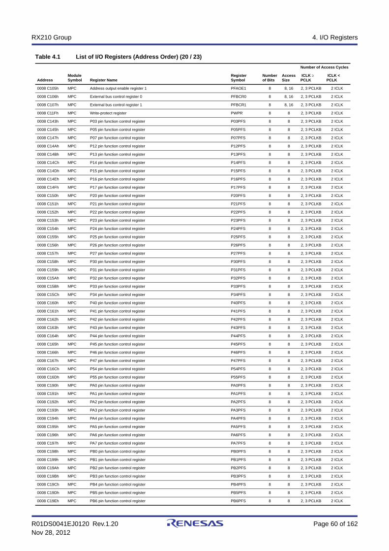
R01DS0041EJ0120 Rev.1.20 Page 60 of 162Nov 28, 2012
RX210 Group 4. I/O Registers
0008 C105h MPC Address output enable register 1 PFAOE1 8 8, 16 2, 3 PCLKB 2 ICLK
0008 C106h MPC External bus control register 0 PFBCR0 8 8, 16 2, 3 PCLKB 2 ICLK
0008 C107h MPC External bus control register 1 PFBCR1 8 8, 16 2, 3 PCLKB 2 ICLK
0008 C11Fh MPC Write-protect register PWPR 8 8 2, 3 PCLKB 2 ICLK
0008 C143h MPC P03 pin function control register P03PFS 8 8 2, 3 PCLKB 2 ICLK
0008 C145h MPC P05 pin function control register P05PFS 8 8 2, 3 PCLKB 2 ICLK
0008 C147h MPC P07 pin function control register P07PFS 8 8 2, 3 PCLKB 2 ICLK
0008 C14Ah MPC P12 pin function control register P12PFS 8 8 2, 3 PCLKB 2 ICLK
0008 C14Bh MPC P13 pin function control register P13PFS 8 8 2, 3 PCLKB 2 ICLK
0008 C14Ch MPC P14 pin function control register P14PFS 8 8 2, 3 PCLKB 2 ICLK
0008 C14Dh MPC P15 pin function control register P15PFS 8 8 2, 3 PCLKB 2 ICLK
0008 C14Eh MPC P16 pin function control register P16PFS 8 8 2, 3 PCLKB 2 ICLK
0008 C14Fh MPC P17 pin function control register P17PFS 8 8 2, 3 PCLKB 2 ICLK
0008 C150h MPC P20 pin function control register P20PFS 8 8 2, 3 PCLKB 2 ICLK
0008 C151h MPC P21 pin function control register P21PFS 8 8 2, 3 PCLKB 2 ICLK
0008 C152h MPC P22 pin function control register P22PFS 8 8 2, 3 PCLKB 2 ICLK
0008 C153h MPC P23 pin function control register P23PFS 8 8 2, 3 PCLKB 2 ICLK
0008 C154h MPC P24 pin function control register P24PFS 8 8 2, 3 PCLKB 2 ICLK
0008 C155h MPC P25 pin function control register P25PFS 8 8 2, 3 PCLKB 2 ICLK
0008 C156h MPC P26 pin function control register P26PFS 8 8 2, 3 PCLKB 2 ICLK
0008 C157h MPC P27 pin function control register P27PFS 8 8 2, 3 PCLKB 2 ICLK
0008 C158h MPC P30 pin function control register P30PFS 8 8 2, 3 PCLKB 2 ICLK
0008 C159h MPC P31 pin function control register P31PFS 8 8 2, 3 PCLKB 2 ICLK
0008 C15Ah MPC P32 pin function control register P32PFS 8 8 2, 3 PCLKB 2 ICLK
0008 C15Bh MPC P33 pin function control register P33PFS 8 8 2, 3 PCLKB 2 ICLK
0008 C15Ch MPC P34 pin function control register P34PFS 8 8 2, 3 PCLKB 2 ICLK
0008 C160h MPC P40 pin function control register P40PFS 8 8 2, 3 PCLKB 2 ICLK
0008 C161h MPC P41 pin function control register P41PFS 8 8 2, 3 PCLKB 2 ICLK
0008 C162h MPC P42 pin function control register P42PFS 8 8 2, 3 PCLKB 2 ICLK
0008 C163h MPC P43 pin function control register P43PFS 8 8 2, 3 PCLKB 2 ICLK
0008 C164h MPC P44 pin function control register P44PFS 8 8 2, 3 PCLKB 2 ICLK
0008 C165h MPC P45 pin function control register P45PFS 8 8 2, 3 PCLKB 2 ICLK
0008 C166h MPC P46 pin function control register P46PFS 8 8 2, 3 PCLKB 2 ICLK
0008 C167h MPC P47 pin function control register P47PFS 8 8 2, 3 PCLKB 2 ICLK
0008 C16Ch MPC P54 pin function control register P54PFS 8 8 2, 3 PCLKB 2 ICLK
0008 C16Dh MPC P55 pin function control register P55PFS 8 8 2, 3 PCLKB 2 ICLK
0008 C190h MPC PA0 pin function control register PA0PFS 8 8 2, 3 PCLKB 2 ICLK
0008 C191h MPC PA1 pin function control register PA1PFS 8 8 2, 3 PCLKB 2 ICLK
0008 C192h MPC PA2 pin function control register PA2PFS 8 8 2, 3 PCLKB 2 ICLK
0008 C193h MPC PA3 pin function control register PA3PFS 8 8 2, 3 PCLKB 2 ICLK
0008 C194h MPC PA4 pin function control register PA4PFS 8 8 2, 3 PCLKB 2 ICLK
0008 C195h MPC PA5 pin function control register PA5PFS 8 8 2, 3 PCLKB 2 ICLK
0008 C196h MPC PA6 pin function control register PA6PFS 8 8 2, 3 PCLKB 2 ICLK
0008 C197h MPC PA7 pin function control register PA7PFS 8 8 2, 3 PCLKB 2 ICLK
0008 C198h MPC PB0 pin function control register PB0PFS 8 8 2, 3 PCLKB 2 ICLK
0008 C199h MPC PB1 pin function control register PB1PFS 8 8 2, 3 PCLKB 2 ICLK
0008 C19Ah MPC PB2 pin function control register PB2PFS 8 8 2, 3 PCLKB 2 ICLK
0008 C19Bh MPC PB3 pin function control register PB3PFS 8 8 2, 3 PCLKB 2 ICLK
0008 C19Ch MPC PB4 pin function control register PB4PFS 8 8 2, 3 PCLKB 2 ICLK
0008 C19Dh MPC PB5 pin function control register PB5PFS 8 8 2, 3 PCLKB 2 ICLK
0008 C19Eh MPC PB6 pin function control register PB6PFS 8 8 2, 3 PCLKB 2 ICLK
Table 4.1 List of I/O Registers (Address Order) (20 / 23)
AddressModule Symbol Register Name
Register Symbol
Number of Bits
Access Size
Number of Access Cycles
ICLK PCLK
ICLK <PCLK
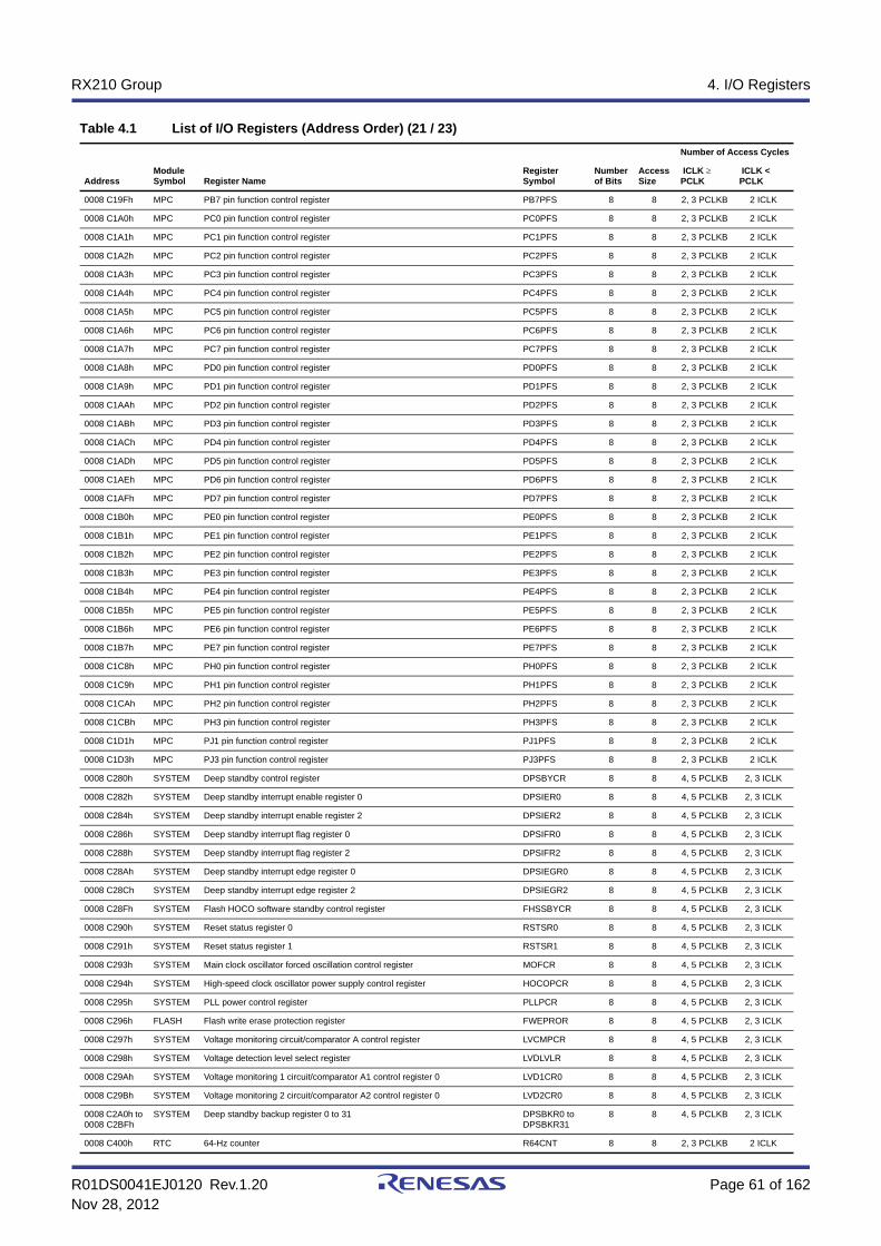
R01DS0041EJ0120 Rev.1.20 Page 61 of 162Nov 28, 2012
RX210 Group 4. I/O Registers
0008 C19Fh MPC PB7 pin function control register PB7PFS 8 8 2, 3 PCLKB 2 ICLK
0008 C1A0h MPC PC0 pin function control register PC0PFS 8 8 2, 3 PCLKB 2 ICLK
0008 C1A1h MPC PC1 pin function control register PC1PFS 8 8 2, 3 PCLKB 2 ICLK
0008 C1A2h MPC PC2 pin function control register PC2PFS 8 8 2, 3 PCLKB 2 ICLK
0008 C1A3h MPC PC3 pin function control register PC3PFS 8 8 2, 3 PCLKB 2 ICLK
0008 C1A4h MPC PC4 pin function control register PC4PFS 8 8 2, 3 PCLKB 2 ICLK
0008 C1A5h MPC PC5 pin function control register PC5PFS 8 8 2, 3 PCLKB 2 ICLK
0008 C1A6h MPC PC6 pin function control register PC6PFS 8 8 2, 3 PCLKB 2 ICLK
0008 C1A7h MPC PC7 pin function control register PC7PFS 8 8 2, 3 PCLKB 2 ICLK
0008 C1A8h MPC PD0 pin function control register PD0PFS 8 8 2, 3 PCLKB 2 ICLK
0008 C1A9h MPC PD1 pin function control register PD1PFS 8 8 2, 3 PCLKB 2 ICLK
0008 C1AAh MPC PD2 pin function control register PD2PFS 8 8 2, 3 PCLKB 2 ICLK
0008 C1ABh MPC PD3 pin function control register PD3PFS 8 8 2, 3 PCLKB 2 ICLK
0008 C1ACh MPC PD4 pin function control register PD4PFS 8 8 2, 3 PCLKB 2 ICLK
0008 C1ADh MPC PD5 pin function control register PD5PFS 8 8 2, 3 PCLKB 2 ICLK
0008 C1AEh MPC PD6 pin function control register PD6PFS 8 8 2, 3 PCLKB 2 ICLK
0008 C1AFh MPC PD7 pin function control register PD7PFS 8 8 2, 3 PCLKB 2 ICLK
0008 C1B0h MPC PE0 pin function control register PE0PFS 8 8 2, 3 PCLKB 2 ICLK
0008 C1B1h MPC PE1 pin function control register PE1PFS 8 8 2, 3 PCLKB 2 ICLK
0008 C1B2h MPC PE2 pin function control register PE2PFS 8 8 2, 3 PCLKB 2 ICLK
0008 C1B3h MPC PE3 pin function control register PE3PFS 8 8 2, 3 PCLKB 2 ICLK
0008 C1B4h MPC PE4 pin function control register PE4PFS 8 8 2, 3 PCLKB 2 ICLK
0008 C1B5h MPC PE5 pin function control register PE5PFS 8 8 2, 3 PCLKB 2 ICLK
0008 C1B6h MPC PE6 pin function control register PE6PFS 8 8 2, 3 PCLKB 2 ICLK
0008 C1B7h MPC PE7 pin function control register PE7PFS 8 8 2, 3 PCLKB 2 ICLK
0008 C1C8h MPC PH0 pin function control register PH0PFS 8 8 2, 3 PCLKB 2 ICLK
0008 C1C9h MPC PH1 pin function control register PH1PFS 8 8 2, 3 PCLKB 2 ICLK
0008 C1CAh MPC PH2 pin function control register PH2PFS 8 8 2, 3 PCLKB 2 ICLK
0008 C1CBh MPC PH3 pin function control register PH3PFS 8 8 2, 3 PCLKB 2 ICLK
0008 C1D1h MPC PJ1 pin function control register PJ1PFS 8 8 2, 3 PCLKB 2 ICLK
0008 C1D3h MPC PJ3 pin function control register PJ3PFS 8 8 2, 3 PCLKB 2 ICLK
0008 C280h SYSTEM Deep standby control register DPSBYCR 8 8 4, 5 PCLKB 2, 3 ICLK
0008 C282h SYSTEM Deep standby interrupt enable register 0 DPSIER0 8 8 4, 5 PCLKB 2, 3 ICLK
0008 C284h SYSTEM Deep standby interrupt enable register 2 DPSIER2 8 8 4, 5 PCLKB 2, 3 ICLK
0008 C286h SYSTEM Deep standby interrupt flag register 0 DPSIFR0 8 8 4, 5 PCLKB 2, 3 ICLK
0008 C288h SYSTEM Deep standby interrupt flag register 2 DPSIFR2 8 8 4, 5 PCLKB 2, 3 ICLK
0008 C28Ah SYSTEM Deep standby interrupt edge register 0 DPSIEGR0 8 8 4, 5 PCLKB 2, 3 ICLK
0008 C28Ch SYSTEM Deep standby interrupt edge register 2 DPSIEGR2 8 8 4, 5 PCLKB 2, 3 ICLK
0008 C28Fh SYSTEM Flash HOCO software standby control register FHSSBYCR 8 8 4, 5 PCLKB 2, 3 ICLK
0008 C290h SYSTEM Reset status register 0 RSTSR0 8 8 4, 5 PCLKB 2, 3 ICLK
0008 C291h SYSTEM Reset status register 1 RSTSR1 8 8 4, 5 PCLKB 2, 3 ICLK
0008 C293h SYSTEM Main clock oscillator forced oscillation control register MOFCR 8 8 4, 5 PCLKB 2, 3 ICLK
0008 C294h SYSTEM High-speed clock oscillator power supply control register HOCOPCR 8 8 4, 5 PCLKB 2, 3 ICLK
0008 C295h SYSTEM PLL power control register PLLPCR 8 8 4, 5 PCLKB 2, 3 ICLK
0008 C296h FLASH Flash write erase protection register FWEPROR 8 8 4, 5 PCLKB 2, 3 ICLK
0008 C297h SYSTEM Voltage monitoring circuit/comparator A control register LVCMPCR 8 8 4, 5 PCLKB 2, 3 ICLK
0008 C298h SYSTEM Voltage detection level select register LVDLVLR 8 8 4, 5 PCLKB 2, 3 ICLK
0008 C29Ah SYSTEM Voltage monitoring 1 circuit/comparator A1 control register 0 LVD1CR0 8 8 4, 5 PCLKB 2, 3 ICLK
0008 C29Bh SYSTEM Voltage monitoring 2 circuit/comparator A2 control register 0 LVD2CR0 8 8 4, 5 PCLKB 2, 3 ICLK
0008 C2A0h to 0008 C2BFh
SYSTEM Deep standby backup register 0 to 31 DPSBKR0 to DPSBKR31
8 8 4, 5 PCLKB 2, 3 ICLK
0008 C400h RTC 64-Hz counter R64CNT 8 8 2, 3 PCLKB 2 ICLK
Table 4.1 List of I/O Registers (Address Order) (21 / 23)
AddressModule Symbol Register Name
Register Symbol
Number of Bits
Access Size
Number of Access Cycles
ICLK PCLK
ICLK <PCLK

R01DS0041EJ0120 Rev.1.20 Page 62 of 162Nov 28, 2012
RX210 Group 4. I/O Registers
0008 C402h RTC Second counter RSECCNT 8 8 2, 3 PCLKB 2 ICLK
0008 C404h RTC Minute counter RMINCNT 8 8 2, 3 PCLKB 2 ICLK
0008 C406h RTC Hour counter RHRCNT 8 8 2, 3 PCLKB 2 ICLK
0008 C408h RTC Day-of-week counter RWKCNT 8 8 2, 3 PCLKB 2 ICLK
0008 C40Ah RTC Date counter RDAYCNT 8 8 2, 3 PCLKB 2 ICLK
0008 C40Ch RTC Month counter RMONCNT 8 8 2, 3 PCLKB 2 ICLK
0008 C40Eh RTC Year counter RYRCNT 16 16 2, 3 PCLKB 2 ICLK
0008 C410h RTC Second alarm register RSECAR 8 8 2, 3 PCLKB 2 ICLK
0008 C412h RTC Minute alarm register RMINAR 8 8 2, 3 PCLKB 2 ICLK
0008 C414h RTC Hour alarm register RHRAR 8 8 2, 3 PCLKB 2 ICLK
0008 C416h RTC Day-of-week alarm register RWKAR 8 8 2, 3 PCLKB 2 ICLK
0008 C418h RTC Date alarm register RDAYAR 8 8 2, 3 PCLKB 2 ICLK
0008 C41Ah RTC Month alarm register RMONAR 8 8 2, 3 PCLKB 2 ICLK
0008 C41Ch RTC Year alarm register RYRAR 16 16 2, 3 PCLKB 2 ICLK
0008 C41Eh RTC Year alarm enable register RYRAREN 8 8 2, 3 PCLKB 2 ICLK
0008 C422h RTC RTC control register 1 RCR1 8 8 2, 3 PCLKB 2 ICLK
0008 C424h RTC RTC control register 2 RCR2 8 8 2, 3 PCLKB 2 ICLK
0008 C426h RTC RTC control register 3 RCR3 8 8 2, 3 PCLKB 2 ICLK
0008 C42Eh RTC Time error adjustment register RADJ 8 8 2, 3 PCLKB 2 ICLK
0008 C440h RTC Time capture control register 0 RTCCR0 8 8 2, 3 PCLKB 2 ICLK
0008 C442h RTC Time capture control register 1 RTCCR1 8 8 2, 3 PCLKB 2 ICLK
0008 C444h RTC Time capture control register 2 RTCCR2 8 8 2, 3 PCLKB 2 ICLK
0008 C452h RTC Second capture register 0 RSECCP0 8 8 2, 3 PCLKB 2 ICLK
0008 C454h RTC Minute capture register 0 RMINCP0 8 8 2, 3 PCLKB 2 ICLK
0008 C456h RTC Hour capture register 0 RHRCP0 8 8 2, 3 PCLKB 2 ICLK
0008 C45Ah RTC Date capture register 0 RDAYCP0 8 8 2, 3 PCLKB 2 ICLK
0008 C45Ch RTC Month capture register 0 RMONCP0 8 8 2, 3 PCLKB 2 ICLK
0008 C462h RTC Second capture register 1 RSECCP1 8 8 2, 3 PCLKB 2 ICLK
0008 C464h RTC Minute capture register 1 RMINCP1 8 8 2, 3 PCLKB 2 ICLK
0008 C466h RTC Hour capture register 1 RHRCP1 8 8 2, 3 PCLKB 2 ICLK
0008 C46Ah RTC Date capture register 1 RDAYCP1 8 8 2, 3 PCLKB 2 ICLK
0008 C46Ch RTC Month capture register 1 RMONCP1 8 8 2, 3 PCLKB 2 ICLK
0008 C472h RTC Second capture register 2 RSECCP2 8 8 2, 3 PCLKB 2 ICLK
0008 C474h RTC Minute capture register 2 RMINCP2 8 8 2, 3 PCLKB 2 ICLK
0008 C476h RTC Hour capture register 2 RHRCP2 8 8 2, 3 PCLKB 2 ICLK
0008 C47Ah RTC Date capture register 2 RDAYCP2 8 8 2, 3 PCLKB 2 ICLK
0008 C47Ch RTC Month capture register 2 RMONCP2 8 8 2, 3 PCLKB 2 ICLK
0008 C500h TEMPS Temperature sensor control register TSCR 8 8 2, 3 PCLKB 2 ICLK
0008 C580h CMPB Comparator B control register 1 CPBCNT1 8 8 2, 3 PCLKB 2 ICLK
0008 C582h CMPB Comparator B flag register CPBFLG 8 8 2, 3 PCLKB 2 ICLK
0008 C583h CMPB Comparator B interrupt control register CPBINT 8 8 2, 3 PCLKB 2 ICLK
0008 C584h CMPB Comparator B filter select register CPBF 8 8 2, 3 PCLKB 2 ICLK
007F C402h FLASH Flash mode register FMODR 8 8 2, 3 FCLK 2 ICLK
007F C410h FLASH Flash access status register FASTAT 8 8 2, 3 FCLK 2 ICLK
007F C411h FLASH Flash access error interrupt enable register FAEINT 8 8 2, 3 FCLK 2 ICLK
007F C412h FLASH Flash ready interrupt enable register FRDYIE 8 8 2, 3 FCLK 2 ICLK
007F C440h FLASH E2 DataFlash read enable register 0 DFLRE0 16 16 2, 3 FCLK 2 ICLK
007F C450h FLASH E2 DataFlash programming/erasure enable register 0 DFLWE0 16 16 2, 3 FCLK 2 ICLK
007F C454h FLASH FCU RAM enable register FCURAME 16 16 2, 3 FCLK 2 ICLK
007F FFB0h FLASH Flash status register 0 FSTATR0 8 8 2, 3 FCLK 2 ICLK
007F FFB1h FLASH Flash status register 1 FSTATR1 8 8 2, 3 FCLK 2 ICLK
Table 4.1 List of I/O Registers (Address Order) (22 / 23)
AddressModule Symbol Register Name
Register Symbol
Number of Bits
Access Size
Number of Access Cycles
ICLK PCLK
ICLK <PCLK

R01DS0041EJ0120 Rev.1.20 Page 63 of 162Nov 28, 2012
RX210 Group 4. I/O Registers
Note 1. Odd addresses cannot be accessed in 16-bit units. When accessing a register in 16-bit units, access the address of the TMR0 or TMR2 register.Note 2. Odd addresses cannot be accessed in 16-bit units. When accessing a register in 16-bit units, access the address of the TMOCNTL register.
007F FFB2h FLASH Flash P/E mode entry register FENTRYR 16 16 2, 3 FCLK 2 ICLK
007F FFB4h FLASH Flash protection register FPROTR 16 16 2, 3 FCLK 2 ICLK
007F FFB6h FLASH Flash reset register FRESETR 16 16 2, 3 FCLK 2 ICLK
007F FFBAh FLASH FCU command register FCMDR 16 16 2, 3 FCLK 2 ICLK
007F FFC8h FLASH FCU processing switching register FCPSR 16 16 2, 3 FCLK 2 ICLK
007F FFCAh FLASH E2 DataFlash blank check control register DFLBCCNT 16 16 2, 3 FCLK 2 ICLK
007F FFCCh FLASH Flash P/E status register FPESTAT 16 16 2, 3 FCLK 2 ICLK
007F FFCEh FLASH E2 DataFlash blank check status register DFLBCSTAT 16 16 2, 3 FCLK 2 ICLK
007F FFE8h FLASH Peripheral clock notification register PCKAR 16 16 2, 3 FCLK 2 ICLK
Table 4.1 List of I/O Registers (Address Order) (23 / 23)
AddressModule Symbol Register Name
Register Symbol
Number of Bits
Access Size
Number of Access Cycles
ICLK PCLK
ICLK <PCLK

R01DS0041EJ0120 Rev.1.20 Page 64 of 162Nov 28, 2012
RX210 Group 5. Electrical Characteristics
5. Electrical Characteristics
5.1 Absolute Maximum Ratings
Caution: Permanent damage to the LSI may result if absolute maximum ratings are exceeded.To preclude any malfunctions due to noise interferences, insert capacitors of high frequency characteristics between the VCC and VSS pins, between the AVCC0 and AVSS0 pins, and between the VREFH0 and VREFL0 pins. Place capacitors of 0.1 µF or so as close to every power pin and use the shortest and heaviest possible traces.Connect the VCL pin to a VSS pin via a 0.1 µF (±20% accuracy) capacitor. The capacitor must be placed as close to the pin as possible.Note 1. Ports 12, 13, 16, and 17 are 5 V tolerant.Note 2. Connect AVCC0 to VCC. When neither the A/D converter nor the D/A converter is in use, do not leave the AVCC0, VREFH,
VREFH0, AVSS0, VREFL, and VREFL0 pins open. Connect the AVCC0, VREFH, and VREFH0 pins to VCC, and the AVSS0, VREFL, and VREFL0 pins to VSS, respectively.
Note 3. The maximum value is 6.5 V.
Table 5.1 Absolute Maximum RatingsConditions: VSS = AVSS0 = VREFL = VREFL0 = 0 V
Item Symbol Value Unit
Power supply voltage VCC –0.3 to +6.5 V
Input voltage (except for ports for 5 V tolerant*1) Vin –0.3 to VCC +0.3*3 V
Input voltage (ports for 5 V tolerant*1) Vin –0.3 to +6.5 V
Reference power supply voltage VREFH, VREFH0 –0.3 to VCC +0.3*3 V
Analog power supply voltage AVCC0*2 –0.3 to +6.5 V
Analog input voltage VAN –0.3 to VCC +0.3*3 V
Operating temperature Topr –40 to +105 °C
Storage temperature Tstg –55 to +125 °C
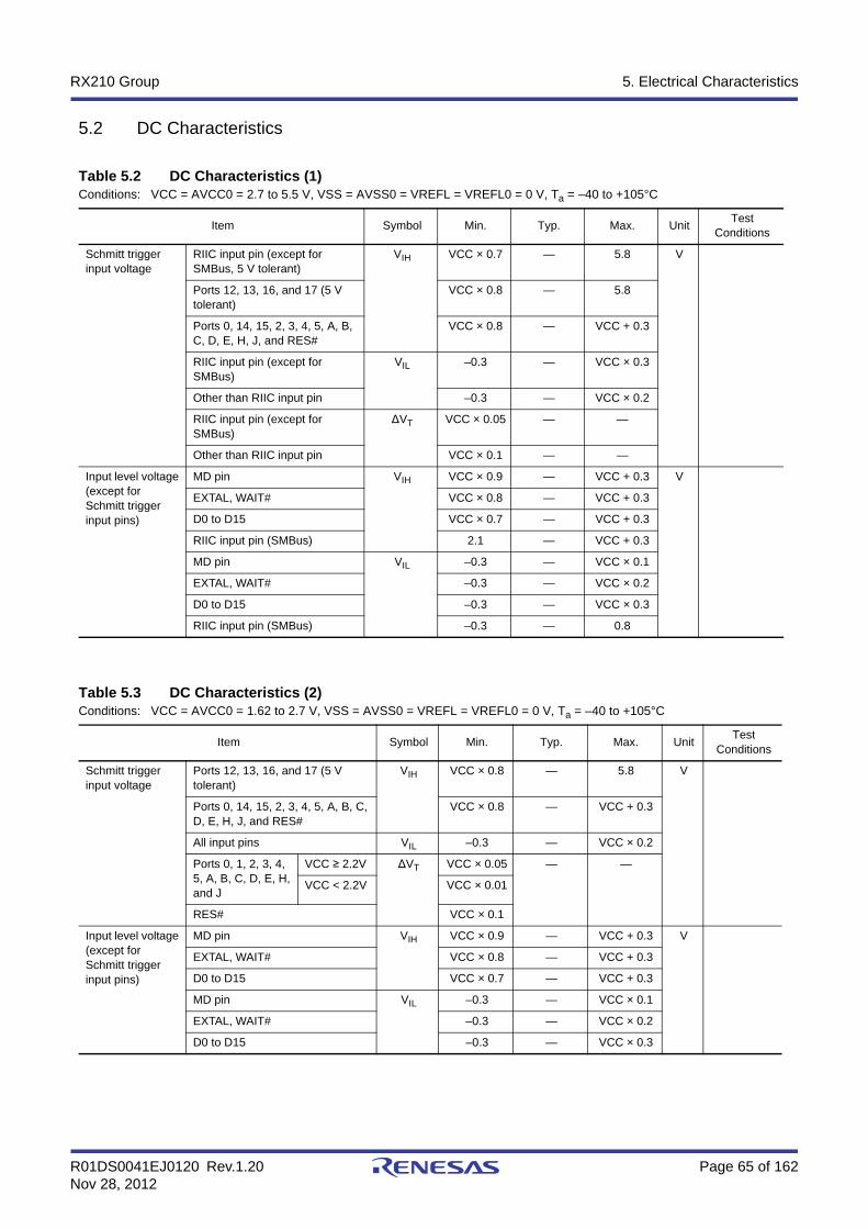
R01DS0041EJ0120 Rev.1.20 Page 65 of 162Nov 28, 2012
RX210 Group 5. Electrical Characteristics
5.2 DC Characteristics
Table 5.2 DC Characteristics (1)Conditions: VCC = AVCC0 = 2.7 to 5.5 V, VSS = AVSS0 = VREFL = VREFL0 = 0 V, Ta = –40 to +105°C
Item Symbol Min. Typ. Max. UnitTest
Conditions
Schmitt trigger input voltage
RIIC input pin (except for SMBus, 5 V tolerant)
VIH VCC × 0.7 — 5.8 V
Ports 12, 13, 16, and 17 (5 V tolerant)
VCC × 0.8 — 5.8
Ports 0, 14, 15, 2, 3, 4, 5, A, B, C, D, E, H, J, and RES#
VCC × 0.8 — VCC + 0.3
RIIC input pin (except for SMBus)
VIL –0.3 — VCC × 0.3
Other than RIIC input pin –0.3 — VCC × 0.2
RIIC input pin (except for SMBus)
ΔVT VCC × 0.05 — —
Other than RIIC input pin VCC × 0.1 — —
Input level voltage (except for Schmitt trigger input pins)
MD pin VIH VCC × 0.9 — VCC + 0.3 V
EXTAL, WAIT# VCC × 0.8 — VCC + 0.3
D0 to D15 VCC × 0.7 — VCC + 0.3
RIIC input pin (SMBus) 2.1 — VCC + 0.3
MD pin VIL –0.3 — VCC × 0.1
EXTAL, WAIT# –0.3 — VCC × 0.2
D0 to D15 –0.3 — VCC × 0.3
RIIC input pin (SMBus) –0.3 — 0.8
Table 5.3 DC Characteristics (2)Conditions: VCC = AVCC0 = 1.62 to 2.7 V, VSS = AVSS0 = VREFL = VREFL0 = 0 V, Ta = –40 to +105°C
Item Symbol Min. Typ. Max. UnitTest
Conditions
Schmitt trigger input voltage
Ports 12, 13, 16, and 17 (5 V tolerant)
VIH VCC × 0.8 — 5.8 V
Ports 0, 14, 15, 2, 3, 4, 5, A, B, C, D, E, H, J, and RES#
VCC × 0.8 — VCC + 0.3
All input pins VIL –0.3 — VCC × 0.2
Ports 0, 1, 2, 3, 4, 5, A, B, C, D, E, H, and J
VCC ≥ 2.2V ΔVT VCC × 0.05 — —
VCC < 2.2V VCC × 0.01
RES# VCC × 0.1
Input level voltage (except for Schmitt trigger input pins)
MD pin VIH VCC × 0.9 — VCC + 0.3 V
EXTAL, WAIT# VCC × 0.8 — VCC + 0.3
D0 to D15 VCC × 0.7 — VCC + 0.3
MD pin VIL –0.3 — VCC × 0.1
EXTAL, WAIT# –0.3 — VCC × 0.2
D0 to D15 –0.3 — VCC × 0.3

R01DS0041EJ0120 Rev.1.20 Page 66 of 162Nov 28, 2012
RX210 Group 5. Electrical Characteristics
[Chip versions A and C]
Note 1. Supply current values do not include output charge/discharge current from all pins. The values apply when internal pull-up MOSs are in the off state.
Note 2. Clock supply to the peripheral functions is stopped. This does not include BGO operation. The clock source is PLL and the VCO oscillation frequency is 100 MHz. BCLK, FCLK, and PCLK are set to divided by 64.
Note 3. Clocks are supplied to the peripheral functions. This does not include BGO operation. The clock source is PLL and the VCO oscillation frequency is 100 MHz. BCLK, FCLK, and PCLK are ICLK divided by 2.
Note 4. This is the increase if data is programmed to or erasing from the ROM or E2 DataFlash during program execution.
Table 5.4 DC Characteristics (3)Conditions: VCC = AVCC0 = 1.62 to 5.5 V, VSS = AVSS0 = VREFL = VREFL0 = 0 V, Ta = –40 to +105°C
Item Symbol Min. Typ. Max. Unit Test Conditions
Input leakage current
RES#, MD pin, NMI Iin — — 1.0 µA Vin = 0 V, VCC
Three-state leakage current (off-state)
Port 4 ITSI — — 1.0 µA Vin = 0 V, VCC
Other pins except for ports for 5 V tolerant and port 4
— — 0.2
Ports for 5 V tolerant — — 1.0 Vin = 0 V, 5.8 V
Input capacitance All input pins(except for ports 12, 13, 16, 17, port 4, ports A1, A3, A4, and port E)
Cin — — 15 pF Vin = 0 V, f = 1 MHz, Ta = 25°C
Ports 12, 13, 16, 17, port 4, ports A1, A3, A4, and port E
— — 30
Table 5.5 DC Characteristics (4)Conditions: VCC = AVCC0 = 1.62 to 5.5 V, VSS = AVSS0 = VREFL = VREFL0 = 0 V, Ta = –40 to +105°C
Item Symbol
VCC
Unit Test Conditions1.62 to 2.7 V 2.7 to 4.0 V 4.0 to 5.5 V
Min. Max. Min. Max. Min. Max.
Input pull-up MOS current
All ports (except for port 35)
Ip –150 –5 –200 –10 –400 –50 µA Vin = 0 V
Table 5.6 DC Characteristics (5)Conditions: VCC = AVCC0 = 2.7 to 5.5 V, VSS = AVSS0 = VREFL = VREFL0 = 0 V, Ta = –40 to +105°C
Item Symbol Typ. Max. UnitTest
Conditions
Supply current*1
High-speed operating mode
Normal operating mode
No peripheral operation*2
ICLK = 50 MHz ICC 10 — mA
All peripheral operation: Normal*3
ICLK = 50 MHz 31.5 —
All peripheral operation: Max.*3
ICLK = 50 MHz — 55
Sleep mode No peripheral operation
ICLK = 50 MHz 7.5 —
All peripheral operation: Normal
ICLK = 50 MHz 17.5 —
All-module clock stop mode ICLK = 50 MHz 6.7 —
Increase during BGO operation*4 25 —

R01DS0041EJ0120 Rev.1.20 Page 67 of 162Nov 28, 2012
RX210 Group 5. Electrical Characteristics
[Chip versions A and C]
Note 1. Supply current values do not include output charge/discharge current from all pins. The values apply when internal pull-up MOSs are in the off state.
Note 2. Clock supply to the peripheral functions is stopped. This does not include BGO operation. The clock source is PLL and the VCO oscillation frequencies are 64 MHz and 40 MHz, respectively. BCLK, FCLK, and PCLK are set to divided by 64.
Note 3. Clocks are supplied to the peripheral functions. This does not include BGO operation. The clock source is PLL and the VCO oscillation frequencies are 64 MHz and 40 MHz, respectively. BCLK, FCLK, and PCLK are ICLK divided by 1.
Note 4. This is the increase if data is programmed to or erasing from the ROM or E2 DataFlash during program execution.
Table 5.7 DC Characteristics (6)Conditions: VCC = AVCC0 = 1.62 to 5.5 V, VSS = AVSS0 = VREFL = VREFL0 = 0 V, Ta = –40 to +105°C
Item Symbol Typ. Max. UnitTest
Conditions
Supply current*1
Medium-speed operating modes 1A and 1B
Normal operating mode
No peripheral operation*2
ICLK = 32 MHz ICC 7.0 — mA
ICLK = 20 MHz 6.0 —
All peripheral operation: Normal*3
ICLK = 32 MHz 26 —
ICLK = 20 MHz 18.5 —
All peripheral operation: Max.*3
ICLK = 32 MHz — 40
ICLK = 20 MHz — 30
Sleep mode No peripheral operation
ICLK = 32 MHz 5.0 —
ICLK = 20 MHz 4.6 —
All peripheral operation: Normal
ICLK = 32 MHz 15.5 —
ICLK = 20 MHz 12 —
All-module clock stop mode ICLK = 32 MHz 4.5 —
ICLK = 20 MHz 4.3 —
Increase during BGO operation*4
Medium-speed operating mode 1A 25 —
Medium-speed operating mode 1B 20 —
Low-speed operating mode 1
Normal operating mode
No peripheral operation*5
ICLK = 1 MHz 0.68 —
All peripheral operation: Normal*6
ICLK = 1 MHz 2.4 —
All peripheral operation: Max.*6
ICLK = 1 MHz — 7
Sleep mode No peripheral operation
ICLK = 1 MHz 0.6 —
All peripheral operation: Normal
ICLK = 1 MHz 2 —
All-module clock stop mode 0.58 —
Low-speed operating mode 2
Normal operating mode
No peripheral operation*7
ICLK = 32 kHz 0.024 —
All peripheral operation: Normal*8
ICLK = 32 kHz 0.05 —
All peripheral operation: Max.*8
ICLK = 32 kHz — 3*9
Sleep mode No peripheral operation
ICLK = 32 kHz 0.02 —
All peripheral operation: Normal
ICLK = 32 kHz 0.04 —
All-module clock stop mode 0.018 —

R01DS0041EJ0120 Rev.1.20 Page 68 of 162Nov 28, 2012
RX210 Group 5. Electrical Characteristics
Note 5. Clock supply to the peripheral functions is stopped. This does not include BGO operation. The clock source is HOCO and the oscillation frequency is 32 MHz. BCLK, FCLK, and PCLK are set to divided by 64.
Note 6. Clocks are supplied to the peripheral functions. This does not include BGO operation. The clock source is HOCO and the oscillation frequency is 32 MHz. BCLK, FCLK, and PCLK are ICLK divided by 1.
Note 7. Clock supply to the peripheral functions is stopped. This does not include BGO operation. The clock source is the sub oscillation circuit. BCLK, FCLK, and PCLK are set to divided by 64.
Note 8. Clocks are supplied to the peripheral functions. This does not include BGO operation. The clock source is the sub oscillation circuit. BCLK, FCLK, and PCLK are ICLK divided by 1.
Note 9. Value when the main clock continues oscillating at 12.5 MHz.
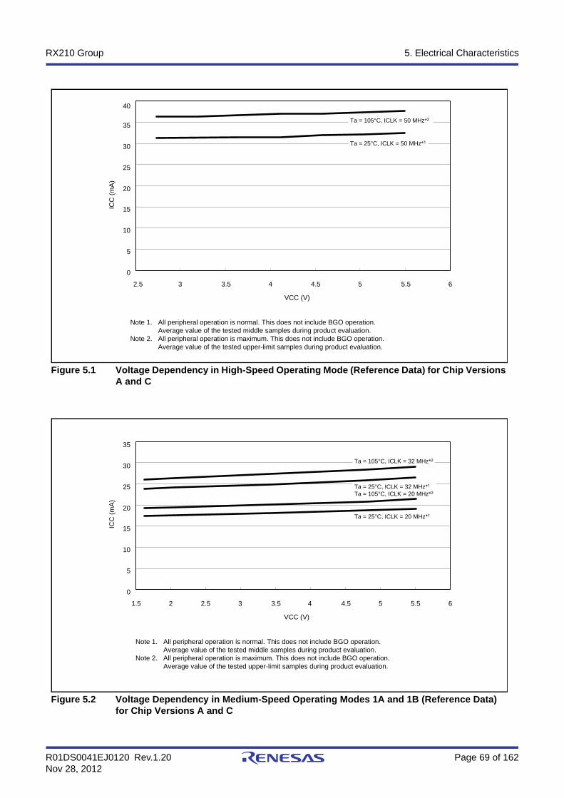
R01DS0041EJ0120 Rev.1.20 Page 69 of 162Nov 28, 2012
RX210 Group 5. Electrical Characteristics
Figure 5.1 Voltage Dependency in High-Speed Operating Mode (Reference Data) for Chip Versions A and C
Figure 5.2 Voltage Dependency in Medium-Speed Operating Modes 1A and 1B (Reference Data) for Chip Versions A and C
VCC (V)
0
5
10
15
20
25
30
35
2.5 3 3.5 4 4.5 5 5.5 6
ICC
(m
A)
40
Ta = 105°C, ICLK = 50 MHz*2
Ta = 25°C, ICLK = 50 MHz*1
Note 1. All peripheral operation is normal. This does not include BGO operation. Average value of the tested middle samples during product evaluation.
Note 2. All peripheral operation is maximum. This does not include BGO operation. Average value of the tested upper-limit samples during product evaluation.
VCC (V)
0
5
10
15
20
25
30
35
2.5 3 3.5 4 4.5 5 5.5 6
ICC
(m
A)
Ta = 25°C, ICLK = 20 MHz*1
Ta = 25°C, ICLK = 32 MHz*1
Ta = 105°C, ICLK = 20 MHz*2
Ta = 105°C, ICLK = 32 MHz*2
1.5 2
Note 1. All peripheral operation is normal. This does not include BGO operation. Average value of the tested middle samples during product evaluation.
Note 2. All peripheral operation is maximum. This does not include BGO operation. Average value of the tested upper-limit samples during product evaluation.

R01DS0041EJ0120 Rev.1.20 Page 70 of 162Nov 28, 2012
RX210 Group 5. Electrical Characteristics
Figure 5.3 Voltage Dependency in Low-Speed Operating Mode 1 (Reference Data) for Chip Versions A and C
Figure 5.4 Voltage Dependency in Low-Speed Operating Mode 2 (Reference Data) for Chip Versions A and C
0
0.5
1
1.5
2
2.5
3
3.5
ICC
(m
A)
4
2.5 3 3.5 4 4.5 5 5.5 61.5 2
Ta = 105°C, ICLK = 1 MHz*2
Ta = 25°C, ICLK = 1 MHz*1
VCC (V)
Note 1. All peripheral operation is normal. Average value of the tested middle samples during product evaluation.
Note 2. All peripheral operation is maximum. Average value of the tested upper-limit samples during product evaluation.
Ta = 105°C, ICLK = 32 kHz*2
Ta = 25°C, ICLK = 32 kHz*1
0
20
40
60
80
100
120
140
160
180
2.5 3 3.5 4 4.5 5 5.5 61.5 2
ICC
(µ
A)
VCC (V)
Note 1. All peripheral operation is normal. Average value of the tested middle samples during product evaluation.
Note 2. All peripheral operation is maximum. Average value of the tested upper-limit samples during product evaluation.

R01DS0041EJ0120 Rev.1.20 Page 71 of 162Nov 28, 2012
RX210 Group 5. Electrical Characteristics
[Chip version B]
Note 1. Supply current values do not include output charge/discharge current from all pins. The values apply when internal pull-up MOSs are in the off state.
Note 2. Clock supply to the peripheral functions is stopped. This does not include BGO operation. The clock source is PLL and the VCO oscillation frequency is 100 MHz. BCLK, FCLK, and PCLK are set to divided by 64.
Note 3. Clocks are supplied to the peripheral functions. This does not include BGO operation. The clock source is PLL and the VCO oscillation frequency is 100 MHz. BCLK, FCLK, and PCLK are ICLK divided by 2.
Note 4. This is the increase if data is programmed to or erasing from the ROM or E2 DataFlash during program execution.
Table 5.8 DC Characteristics (7)Conditions: VCC = AVCC0 = 2.7 to 5.5 V, VSS = AVSS0 = VREFL = VREFL0 = 0 V, Ta = –40 to +105°C
Item Symbol Typ. Max. UnitTest
Conditions
Supply current*1
High-speed operating mode
Normal operating mode
No peripheral operation*2
ICLK = 50 MHz ICC 7.2 — mA
All peripheral operation: Normal*3
ICLK = 50 MHz 23.5 —
All peripheral operation: Max.*3
ICLK = 50 MHz — 45
Sleep mode No peripheral operation
ICLK = 50 MHz 4.3 —
All peripheral operation: Normal
ICLK = 50 MHz 12 —
All-module clock stop mode 3.7 —
Increase during BGO operation*4 20 —
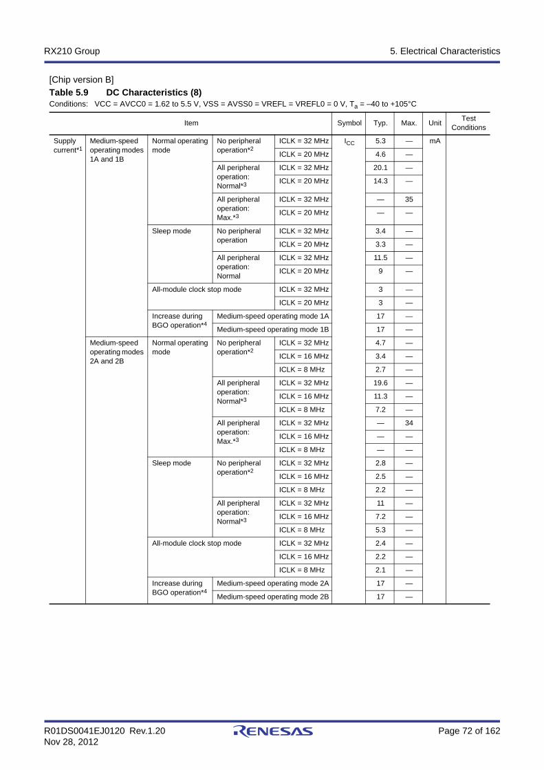
R01DS0041EJ0120 Rev.1.20 Page 72 of 162Nov 28, 2012
RX210 Group 5. Electrical Characteristics
[Chip version B]
Table 5.9 DC Characteristics (8)Conditions: VCC = AVCC0 = 1.62 to 5.5 V, VSS = AVSS0 = VREFL = VREFL0 = 0 V, Ta = –40 to +105°C
Item Symbol Typ. Max. UnitTest
Conditions
Supply current*1
Medium-speed operating modes 1A and 1B
Normal operating mode
No peripheral operation*2
ICLK = 32 MHz ICC 5.3 — mA
ICLK = 20 MHz 4.6 —
All peripheral operation: Normal*3
ICLK = 32 MHz 20.1 —
ICLK = 20 MHz 14.3 —
All peripheral operation: Max.*3
ICLK = 32 MHz — 35
ICLK = 20 MHz — —
Sleep mode No peripheral operation
ICLK = 32 MHz 3.4 —
ICLK = 20 MHz 3.3 —
All peripheral operation: Normal
ICLK = 32 MHz 11.5 —
ICLK = 20 MHz 9 —
All-module clock stop mode ICLK = 32 MHz 3 —
ICLK = 20 MHz 3 —
Increase during BGO operation*4
Medium-speed operating mode 1A 17 —
Medium-speed operating mode 1B 17 —
Medium-speed operating modes 2A and 2B
Normal operating mode
No peripheral operation*2
ICLK = 32 MHz 4.7 —
ICLK = 16 MHz 3.4 —
ICLK = 8 MHz 2.7 —
All peripheral operation: Normal*3
ICLK = 32 MHz 19.6 —
ICLK = 16 MHz 11.3 —
ICLK = 8 MHz 7.2 —
All peripheral operation: Max.*3
ICLK = 32 MHz — 34
ICLK = 16 MHz — —
ICLK = 8 MHz — —
Sleep mode No peripheral operation*2
ICLK = 32 MHz 2.8 —
ICLK = 16 MHz 2.5 —
ICLK = 8 MHz 2.2 —
All peripheral operation: Normal*3
ICLK = 32 MHz 11 —
ICLK = 16 MHz 7.2 —
ICLK = 8 MHz 5.3 —
All-module clock stop mode ICLK = 32 MHz 2.4 —
ICLK = 16 MHz 2.2 —
ICLK = 8 MHz 2.1 —
Increase during BGO operation*4
Medium-speed operating mode 2A 17 —
Medium-speed operating mode 2B 17 —

R01DS0041EJ0120 Rev.1.20 Page 73 of 162Nov 28, 2012
RX210 Group 5. Electrical Characteristics
Note 1. Supply current values do not include output charge/discharge current from all pins. The values apply when internal pull-up MOSs are in the off state.
Note 2. Clock supply to the peripheral functions is stopped. This does not include BGO operation. The clock source is PLL and the VCO oscillation frequencies are 64 MHz and 40 MHz, respectively. BCLK, FCLK, and PCLK are set to divided by 64.
Note 3. Clocks are supplied to the peripheral functions. This does not include BGO operation.The clock source is PLL and the VCO oscillation frequencies are 64 MHz and 40 MHz, respectively. BCLK, FCLK, and PCLK are ICLK divided by 1.
Note 4. This is the increase if data is programmed to or erasing from the ROM or E2 DataFlash during program execution.Note 5. Clock supply to the peripheral functions is stopped. This does not include BGO operation. The clock source is HOCO and the
oscillation frequency is 32 MHz. BCLK, FCLK, and PCLK are set to divided by 64.Note 6. Clocks are supplied to the peripheral functions. This does not include BGO operation. The clock source is HOCO and the
oscillation frequency is 32 MHz. BCLK, FCLK, and PCLK are ICLK divided by 1.Note 7. Clock supply to the peripheral functions is stopped. This does not include BGO operation. The clock source is the sub oscillation
circuit. BCLK, FCLK, and PCLK are set to divided by 64.Note 8. Clocks are supplied to the peripheral functions. This does not include BGO operation. The clock source is the sub oscillation
circuit. BCLK, FCLK, and PCLK are ICLK divided by 1.Note 9. Value when the main clock continues oscillating at 12.5 MHz.
Supply current*1
Low-speed operating mode 1
Normal operating mode
No peripheral operation*5
ICLK = 8 MHz ICC 2 — mA
ICLK = 4 MHz 1.6 —
ICLK = 2 MHz 1.5 —
All peripheral operation: Normal*6
ICLK = 8 MHz 6 —
ICLK = 4 MHz 3.8 —
ICLK = 2 MHz 2.8 —
All peripheral operation: Max. *6
ICLK = 8 MHz — 12
ICLK = 4 MHz — —
ICLK = 2 MHz — —
Sleep mode No peripheral operation
ICLK = 8 MHz 1.5 —
ICLK = 4 MHz 1.4 —
ICLK = 2 MHz 1.3 —
All peripheral operation: Normal
ICLK = 8 MHz 3.6 —
ICLK = 4 MHz 2.7 —
ICLK = 2 MHz 2.2 —
All-module clock stop mode ICLK = 8 MHz 1.4 —
ICLK = 4 MHz 1.3 —
ICLK = 2 MHz 1.2 —
Low-speed operating mode 2
Normal operating mode
No peripheral operation*7
ICLK = 32 kHz 0.021 —
All peripheral operation: Normal*8
ICLK = 32 kHz 0.05 —
All peripheral operation: Max. *8
ICLK = 32 kHz — 3*9
Sleep mode No peripheral operation
ICLK = 32 kHz 0.017 —
All peripheral operation: Normal
ICLK = 32 kHz 0.034 —
All-module clock stop mode 0.016 —
Item Symbol Typ. Max. UnitTest
Conditions
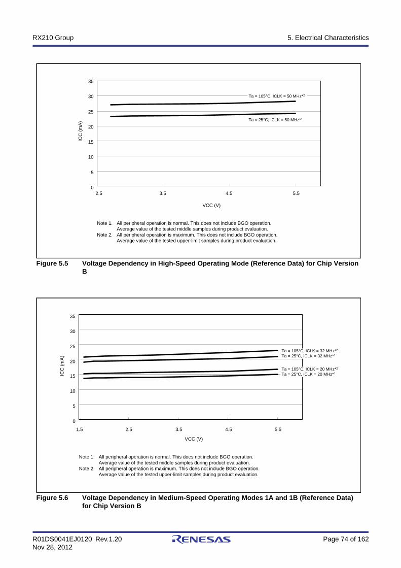
R01DS0041EJ0120 Rev.1.20 Page 74 of 162Nov 28, 2012
RX210 Group 5. Electrical Characteristics
Figure 5.5 Voltage Dependency in High-Speed Operating Mode (Reference Data) for Chip Version B
Figure 5.6 Voltage Dependency in Medium-Speed Operating Modes 1A and 1B (Reference Data) for Chip Version B
0
5
10
15
20
25
30
35
2.5 3.5 4.5 5.5
VCC (V)
ICC
(m
A)
Ta = 105°C, ICLK = 50 MHz*2
Ta = 25°C, ICLK = 50 MHz*1
Note 1. All peripheral operation is normal. This does not include BGO operation. Average value of the tested middle samples during product evaluation.
Note 2. All peripheral operation is maximum. This does not include BGO operation. Average value of the tested upper-limit samples during product evaluation.
VCC (V)
0
5
10
15
20
25
30
35
2.5 3.5 4.5 5.5
ICC
(m
A)
1.5
Ta = 105°C, ICLK = 32 MHz*2
Ta = 25°C, ICLK = 32 MHz*1
Ta = 105°C, ICLK = 20 MHz*2
Ta = 25°C, ICLK = 20 MHz*1
Note 1. All peripheral operation is normal. This does not include BGO operation. Average value of the tested middle samples during product evaluation.
Note 2. All peripheral operation is maximum. This does not include BGO operation. Average value of the tested upper-limit samples during product evaluation.
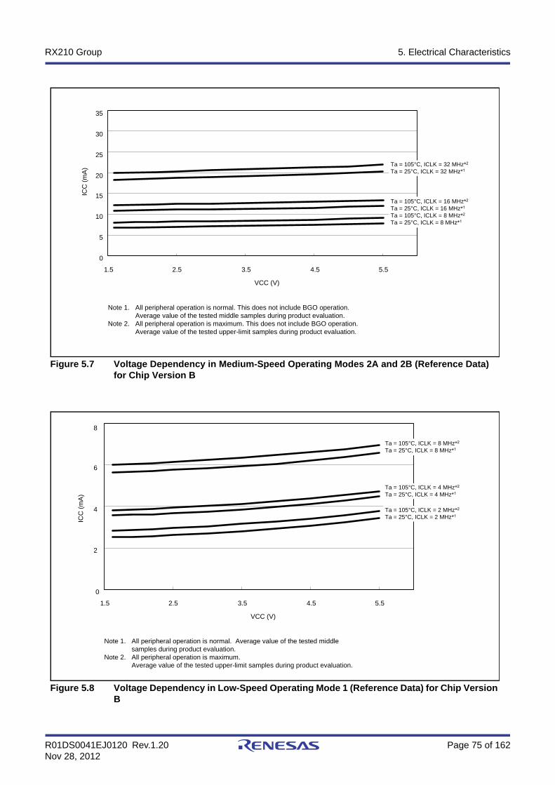
R01DS0041EJ0120 Rev.1.20 Page 75 of 162Nov 28, 2012
RX210 Group 5. Electrical Characteristics
Figure 5.7 Voltage Dependency in Medium-Speed Operating Modes 2A and 2B (Reference Data) for Chip Version B
Figure 5.8 Voltage Dependency in Low-Speed Operating Mode 1 (Reference Data) for Chip Version B
VCC (V)
0
5
10
15
20
25
30
35
2.5 3.5 4.5 5.5
ICC
(m
A)
1.5
Ta = 105°C, ICLK = 16 MHz*2
Ta = 25°C, ICLK = 16 MHz*1
Ta = 105°C, ICLK = 8 MHz*2
Ta = 25°C, ICLK = 8 MHz*1
Ta = 105°C, ICLK = 32 MHz*2
Ta = 25°C, ICLK = 32 MHz*1
Note 1. All peripheral operation is normal. This does not include BGO operation. Average value of the tested middle samples during product evaluation.
Note 2. All peripheral operation is maximum. This does not include BGO operation. Average value of the tested upper-limit samples during product evaluation.
2.5 3.5 4.5 5.51.5
VCC (V)
0
2
4
6
ICC
(m
A)
8
Ta = 105°C, ICLK = 8 MHz*2
Ta = 25°C, ICLK = 8 MHz*1
Ta = 105°C, ICLK = 2 MHz*2
Ta = 25°C, ICLK = 2 MHz*1
Ta = 105°C, ICLK = 4 MHz*2
Ta = 25°C, ICLK = 4 MHz*1
Note 1. All peripheral operation is normal. Average value of the tested middle samples during product evaluation.
Note 2. All peripheral operation is maximum. Average value of the tested upper-limit samples during product evaluation.
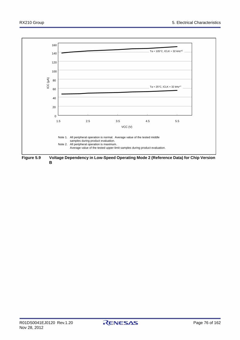
R01DS0041EJ0120 Rev.1.20 Page 76 of 162Nov 28, 2012
RX210 Group 5. Electrical Characteristics
Figure 5.9 Voltage Dependency in Low-Speed Operating Mode 2 (Reference Data) for Chip Version B
VCC (V)
0
20
40
60
80
100
120
140
ICC
(µ
A)
160
2.5 3.5 4.5 5.51.5
Ta = 105°C, ICLK = 32 kHz*2
Ta = 25°C, ICLK = 32 kHz*1
Note 1. All peripheral operation is normal. Average value of the tested middle samples during product evaluation.
Note 2. All peripheral operation is maximum. Average value of the tested upper-limit samples during product evaluation.
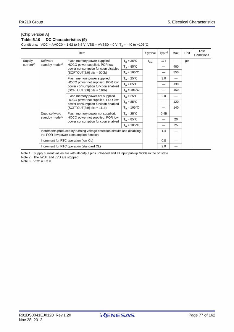
R01DS0041EJ0120 Rev.1.20 Page 77 of 162Nov 28, 2012
RX210 Group 5. Electrical Characteristics
[Chip version A]
Note 1. Supply current values are with all output pins unloaded and all input pull-up MOSs in the off state.Note 2. The IWDT and LVD are stopped.Note 3. VCC = 3.3 V.
Table 5.10 DC Characteristics (9)Conditions: VCC = AVCC0 = 1.62 to 5.5 V, VSS = AVSS0 = 0 V, Ta = –40 to +105°C
Item Symbol Typ.*3 Max. UnitTest
Conditions
Supply current*1
Software standby mode*2
Flash memory power supplied, HOCO power supplied, POR low power consumption function disabled (SOFTCUT[2:0] bits = 000b)
Ta = 25°C ICC 175 — µA
Ta = 85°C — 480
Ta = 105°C — 550
Flash memory power supplied, HOCO power not supplied, POR low power consumption function enabled (SOFTCUT[2:0] bits = 110b)
Ta = 25°C 3.0 —
Ta = 85°C — 130
Ta = 105°C — 150
Flash memory power not supplied, HOCO power not supplied, POR low power consumption function enabled (SOFTCUT[2:0] bits = 111b)
Ta = 25°C 2.0 —
Ta = 85°C — 120
Ta = 105°C — 140
Deep software standby mode*2
Flash memory power not supplied, HOCO power not supplied, POR low power consumption function enabled
Ta = 25°C 0.45
Ta = 85°C — 20
Ta = 105°C — 25
Increments produced by running voltage detection circuits and disabling the POR low power consumption function
1.4 —
Increment for RTC operation (low CL) 0.8 —
Increment for RTC operation (standard CL) 2.0 —

R01DS0041EJ0120 Rev.1.20 Page 78 of 162Nov 28, 2012
RX210 Group 5. Electrical Characteristics
[Chip version C]
Note 1. Supply current values are with all output pins unloaded and all input pull-up MOSs in the off state.Note 2. The IWDT and LVD are stopped.Note 3. VCC = 3.3 V.
Table 5.11 DC Characteristics (10)Conditions: VCC = AVCC0 = 1.62 to 5.5 V, VSS = AVSS0 = 0 V, Ta = –40 to +105°C
Item Symbol Typ.*3 Max. UnitTest
Conditions
Supply current*1
Software standby mode*2
Flash memory power supplied, HOCO power supplied, POR low power consumption function disabled (SOFTCUT[2:0] bits = 000b)
Ta = 25°C ICC 160 235 µA
Ta = 55°C 188 270
Ta = 85°C 220 340
Ta = 105°C 250 445
Flash memory power supplied, HOCO power not supplied, POR low power consumption function enabled (SOFTCUT[2:0] bits = 110b)
Ta = 25°C 2.6 10.5
Ta = 55°C 3.8 22
Ta = 85°C 9.0 80
Ta = 105°C 20 150
Flash memory power not supplied, HOCO power not supplied, POR low power consumption function enabled (SOFTCUT[2:0] bits = 111b)
Ta = 25°C 2.0 8.2
Ta = 55°C 2.9 17
Ta = 85°C 6.8 53
Ta = 105°C 15 115
Deep software standby mode*2
Flash memory power not supplied, HOCO power not supplied, POR low power consumption function enabled
Ta = 25°C 0.5 0.9
Ta = 55°C 0.6 1.2
Ta = 85°C 0.9 20
Ta = 105°C 1.8 25
Increments produced by running voltage detection circuits and disabling the POR low power consumption function
1.4 —
Increment for RTC operation (low CL) 0.8 —
Increment for RTC operation (standard CL) 2.0 —
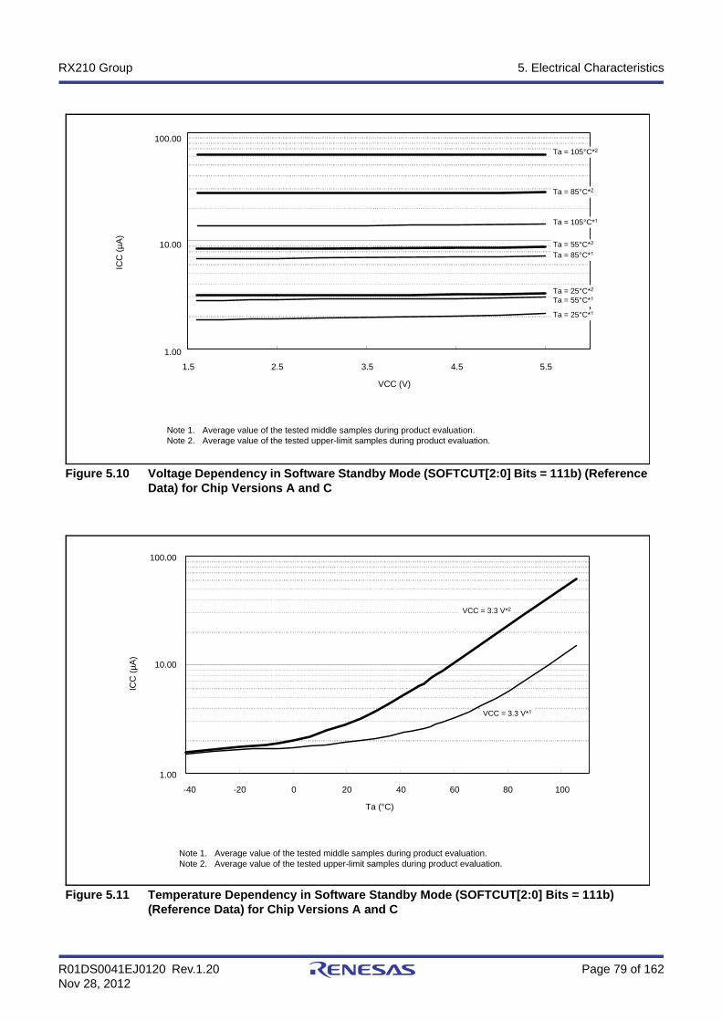
R01DS0041EJ0120 Rev.1.20 Page 79 of 162Nov 28, 2012
RX210 Group 5. Electrical Characteristics
Figure 5.10 Voltage Dependency in Software Standby Mode (SOFTCUT[2:0] Bits = 111b) (Reference Data) for Chip Versions A and C
Figure 5.11 Temperature Dependency in Software Standby Mode (SOFTCUT[2:0] Bits = 111b) (Reference Data) for Chip Versions A and C
VCC (V)
1.00
10.00
ICC
(µ
A)
100.00
2.5 3.5 4.5 5.51.5
Ta = 25°C*2
Ta = 55°C*1
Ta = 105°C*2
Ta = 85°C*2
Ta = 105°C*1
Ta = 55°C*2
Ta = 85°C*1
Ta = 25°C*1
Note 1. Average value of the tested middle samples during product evaluation.Note 2. Average value of the tested upper-limit samples during product evaluation.
1.00
10.00
100.00
-40 -20 0 20 40 60 80 100
Ta (°C)
ICC
(µ
A)
VCC = 3.3 V*2
VCC = 3.3 V*1
Note 1. Average value of the tested middle samples during product evaluation.Note 2. Average value of the tested upper-limit samples during product evaluation.
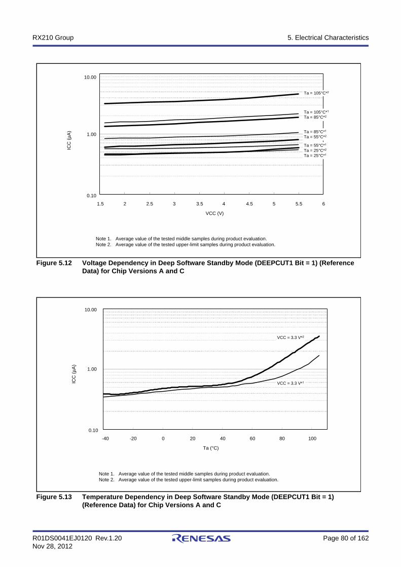
R01DS0041EJ0120 Rev.1.20 Page 80 of 162Nov 28, 2012
RX210 Group 5. Electrical Characteristics
Figure 5.12 Voltage Dependency in Deep Software Standby Mode (DEEPCUT1 Bit = 1) (Reference Data) for Chip Versions A and C
Figure 5.13 Temperature Dependency in Deep Software Standby Mode (DEEPCUT1 Bit = 1) (Reference Data) for Chip Versions A and C
1.5
VCC (V)
2.5 3 3.5 4 4.5 5 5.5 62
0.10
1.00
ICC
(µ
A)
10.00
Ta = 105°C*2
Ta = 85°C*1
Ta = 55°C*2
Ta = 105°C*1
Ta = 85°C*2
Ta = 55°C*1
Ta = 25°C*2
Ta = 25°C*1
Note 1. Average value of the tested middle samples during product evaluation.Note 2. Average value of the tested upper-limit samples during product evaluation.
0.10
1.00
10.00
-40 -20 0 20 40 60 80 100
Ta (°C)
ICC
(µ
A)
VCC = 3.3 V*2
VCC = 3.3 V*1
Note 1. Average value of the tested middle samples during product evaluation.Note 2. Average value of the tested upper-limit samples during product evaluation.

R01DS0041EJ0120 Rev.1.20 Page 81 of 162Nov 28, 2012
RX210 Group 5. Electrical Characteristics
[Chip version B]
Note 1. Supply current values are with all output pins unloaded and all input pull-up MOSs in the off state.Note 2. The IWDT and LVD are stopped.Note 3. VCC = 3.3 V.
Table 5.12 DC Characteristics (11)Conditions: VCC = AVCC0 = 1.62 to 5.5 V, VSS = AVSS0 = 0 V, Ta = –40 to +105°C
Item Symbol Typ.*3 Max. UnitTest
Conditions
Supply current*1
Software standby mode*2
Flash memory power supplied, HOCO power supplied, POR low power consumption function disabled (SOFTCUT[2:0] bits = 000b)
Ta = 25°C ICC 10 18 µA
Ta = 55°C 13 35
Ta = 85°C 20 81
Ta = 105°C 34 154
Flash memory power supplied, HOCO power not supplied, POR low power consumption function enabled (SOFTCUT[2:0] bits = 110b)
Ta = 25°C 1.8 7.7
Ta = 55°C 3.3 20
Ta = 85°C 9.2 60
Ta = 105°C 20 124
Deep software standby mode*2
Flash memory power not supplied, HOCO power not supplied, POR low power consumption function enabled
Ta = 25°C 0.4 0.8
Ta = 55°C 0.5 1.0
Ta = 85°C 0.7 2.5
Ta = 105°C 1.4 6.3
Increments produced by running voltage detection circuits and disabling the POR low power consumption function
1.4 —
Increment for RTC operation (low CL) 0.8 —
Increment for RTC operation (standard CL) 2.0 —

R01DS0041EJ0120 Rev.1.20 Page 82 of 162Nov 28, 2012
RX210 Group 5. Electrical Characteristics
Figure 5.14 Voltage Dependency in Deep Software Standby Mode (SOFTCUT[2:0] Bits = 110b) (Reference Data) for Chip Version B
Figure 5.15 Temperature Dependency in Deep Software Standby Mode (SOFTCUT[2:0] Bits = 110b) (Reference Data) for Chip Version B
VCC (V)
ICC
(µ
A)
1.00
10.00
100.00
1.5 2.5 3 3.5 4 4.5 5 5.5 62
Ta = 25°C*2
Ta = 55°C*1
Ta = 105°C*2
Ta = 85°C*2
Ta = 105°C*1
Ta = 25°C*1
Note 1. Average value of the tested middle samples during product evaluation.Note 2. Average value of the tested upper-limit samples during product evaluation.
Ta = 55°C*2
Ta = 85°C*1
10.00
100.00
-40 -20 0 20 40 60 80 100
Ta (°C)
ICC
(µ
A)
1.00
VCC = 3.3 V*2
VCC = 3.3 V*1
Note 1. Average value of the tested middle samples during product evaluation.Note 2. Average value of the tested upper-limit samples during product evaluation.
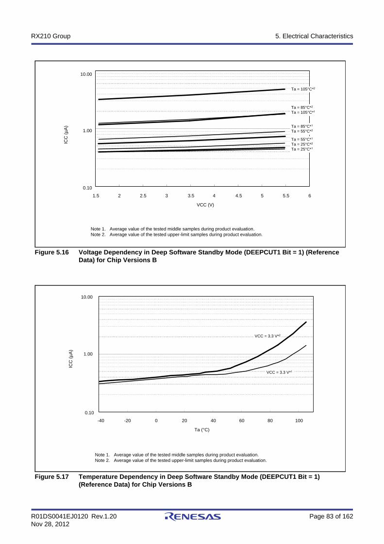
R01DS0041EJ0120 Rev.1.20 Page 83 of 162Nov 28, 2012
RX210 Group 5. Electrical Characteristics
Figure 5.16 Voltage Dependency in Deep Software Standby Mode (DEEPCUT1 Bit = 1) (Reference Data) for Chip Versions B
Figure 5.17 Temperature Dependency in Deep Software Standby Mode (DEEPCUT1 Bit = 1) (Reference Data) for Chip Versions B
Note 1. Average value of the tested middle samples during product evaluation.Note 2. Average value of the tested upper-limit samples during product evaluation.
1.5
VCC (V)
2.5 3 3.5 4 4.5 5 5.5 62
0.10
1.00
ICC
(µ
A)
10.00
Ta = 105°C*2
Ta = 85°C*1
Ta = 55°C*2
Ta = 85°C*2
Ta = 105°C*1
Ta = 55°C*1
Ta = 25°C*2
Ta = 25°C*1
0.10
1.00
10.00
-40 -20 0 20 40 60 80 100
Ta (°C)
ICC
(µ
A)
VCC = 3.3 V*2
VCC = 3.3 V*1
Note 1. Average value of the tested middle samples during product evaluation.Note 2. Average value of the tested upper-limit samples during product evaluation.

R01DS0041EJ0120 Rev.1.20 Page 84 of 162Nov 28, 2012
RX210 Group 5. Electrical Characteristics
Note 1. Total power dissipated by the entire chip (including output currents)
Note: • The values for A/D conversion apply when the sample and hold circuit is not in use.Note 1. The reference power supply current is included in the power supply current value for D/A conversion.
Table 5.13 DC Characteristics (12)Conditions: VCC = AVCC0 = 1.62 to 5.5 V, VSS = AVSS0 = VREFL = VREFL0 = 0 V, Ta = –40 to +105°C
Item Symbol Typ. Max. Unit Test Conditions
Permissible total consumption power*1 Pd — 350 mW Ta = –40 to 85°C
— 150 85°C < Ta ≤ 105°C
Table 5.14 DC Characteristics (13)Conditions: VCC = AVCC0 = 1.62 to 5.5 V, VREFH = 1.8 to AVCC0, VREFH0 = 1.62 to AVCC0,
VSS = AVSS0 = VREFL = VREFL0 = 0 V, Ta = –40 to +105°C
Item Symbol Min. Typ. Max. Unit Test Conditions
Analog power supply current
During A/D conversion AICC — 1.0 3.2 mA
During D/A conversion (per channel)*1 — 0.25 0.75
Temperature sensor — 60 200 µA
Waiting for A/D, D/A conversion (all units) — 0.2 5.0
Reference power supply current
During A/D conversion IREFH,
IREFH0
— 0.1 0.2 mA
Waiting for A/D, D/A conversion (all units) — 0.2 0.4 µA
Table 5.15 DC Characteristics (14)Conditions: VCC = AVCC0, VSS = AVSS0 = VREFL = VREFL0 = 0 V, Ta = –40 to +105°C
Item Symbol Min. Typ. Max. Unit Test Conditions
RAM standby voltage VRAM 1.62 — — V
Table 5.16 DC Characteristics (15)Conditions: VCC = AVCC0 = 0 to 5.5 V, VREFH = VREFH0 = 0 to AVCC0, VSS = AVSS0 = VREFL = VREFL0 = 0 V,
Ta = –40 to +105°C
Item Symbol Min. Typ. Max. Unit Test Conditions
VCC rising gradient SrVCC 0.02 — 20 ms/V At cold start

R01DS0041EJ0120 Rev.1.20 Page 85 of 162Nov 28, 2012
RX210 Group 5. Electrical Characteristics
Figure 5.18 Ripple Waveform
Table 5.17 DC Characteristics (16)Conditions: VCC = AVCC0 = 1.62 to 5.5 V, VSS = AVSS0 = VREFL0 = 0 V, Ta = –40 to +105°C
The ripple voltage must meet the allowable ripple frequency fr(VCC) within the range between the VCC upper limit (5.5 V) and lower limit (1.62 V).When VCC change exceeds VCC ±10%, the allowable voltage change rising/falling gradient dt/dVCC must be met.
Item Symbol Min. Typ. Max. Unit Test Conditions
Allowable ripple frequency fr(VCC) — — 10 kHz Figure 5.18VCC × 0.1 < Vr(VCC) ≤ VCC × 0.2
— — 1 MHz Figure 5.18VCC × 0.05 < Vr(VCC) ≤ VCC × 0.1
— — 10 MHz Figure 5.18Vr(VCC) ≤ VCC × 0.05
Allowable voltage change rising/falling gradient
dt/dVCC 1.0 — — ms/V When VCC change exceeds VCC ±10%
Table 5.18 Permissible Output Currents (1)Conditions: VCC = AVCC0 = 1.62 to 5.5 V, VSS = AVSS0 = VREFL = VREFL0 = 0 V, when total power (mW) < 1000 – 10 × Ta
Item Symbol Max. Unit
Permissible output low current(average value per 1 pin)
Normal output mode IOL 4.0 mA
High-drive output mode 8.0
Permissible output low current(maximum value per 1 pin)
Normal output mode 4.0 mA
High-drive output mode 8.0
Permissible output low current (total) Total of all output pins IOL 80 mA
Permissible output high current(average value per 1 pin)
Normal output mode IOH –4.0 mA
High-drive output mode –8.0
Permissible output high current(maximum value per 1 pin)
Normal output mode –4.0 mA
High-drive output mode –8.0
Permissible output high current (total) Total of all output pins IOH –80 mA
Vr(VCC)VCC
1/fr(VCC)

R01DS0041EJ0120 Rev.1.20 Page 86 of 162Nov 28, 2012
RX210 Group 5. Electrical Characteristics
[Chip version A]
[Chip version A]
[Chip versions B and C]
Table 5.19 Permissible Output Currents (2)Conditions: VCC = AVCC0 = 1.62 to 5.5 V, VSS = AVSS0 = VREFL = VREFL0 = 0 V, when total power (mW) ≥ 1000 – 10 × Ta
Item Symbol Max. Unit
Permissible output low current (average value per 1 pin)
Normal output mode IOL 2.0 mA
High-drive output mode 4.0
Permissible output low current (maximum value per 1 pin)
Normal output mode 2.0 mA
High-drive output mode 4.0
Permissible output low current (total) Total of all output pins IOL 40 mA
Permissible output high current (average value per 1 pin)
Normal output mode IOH –2.0 mA
High-drive output mode –4.0
Permissible output high current (maximum value per 1 pin)
Normal output mode –2.0 mA
High-drive output mode –4.0
Permissible output high current (total) Total of all output pins IOH –40 mA
Table 5.20 Output Values of Voltage (1)Conditions: VCC = AVCC0 = 1.62 to 2.7 V, VSS = AVSS0 = VREFL = VREFL0 = 0 V, Ta = –40 to +105°C
Item Symbol Min. Max. Unit Test Conditions
Output low All output pins (other than RIIC)
Normal output mode VOL — 0.4 V IOL = 0.5 mA
High-drive output mode — 0.4 IOL = 1.0 mA
Output high All output pins Normal output mode VOH VCC – 0.4 — V IOL = –0.5 mA
High-drive output mode VCC – 0.4 — IOL = –1.0 mA
Table 5.21 Output Values of Voltage (2)Conditions: VCC = AVCC0 = 2.7 to 5.5 V, VSS = AVSS0 = VREFL = VREFL0 = 0 V, Ta = –40 to +105°C
Item Symbol Min. Max. UnitTest Conditions
VCC = 2.7 to 4.0 V VCC = 4.0 to 5.5 V
Output low All output pins (other than RIIC)
Normal output mode
VOL — 1.0 V IOL = 3.0 mA IOL = 4.0 mA
High-drive output mode
— 1.0 IOL = 5.0 mA IOL = 8.0 mA
RIIC pins — 0.4 IOL = 3.0 mA
— 0.6 IOL = 6.0 mA
Output high All output pins Normal output mode
VOH VCC – 1.0 — V IOH = – 3.0 mA IOH = – 4.0 mA
High-drive output mode
VCC – 1.0 — IOH = – 5.0 mA IOH = – 8.0 mA
Table 5.22 Output Values of Voltage (3)Conditions: VCC = AVCC0 = 1.62 to 2.7 V, VSS = AVSS0 = VREFL = VREFL0 = 0 V, Ta = –40 to +105°C
Item Symbol Min. Max. Unit Test Conditions
Output low All output pins (other than RIIC)
Normal output mode VOL — 0.3 V IOL = 0.5 mA
High-drive output mode — 0.3 IOL = 1.0 mA
Output high All output pins Normal output mode VOH VCC – 0.3 — V IOL = –0.5 mA
High-drive output mode VCC – 0.3 — IOL = –1.0 mA

R01DS0041EJ0120 Rev.1.20 Page 87 of 162Nov 28, 2012
RX210 Group 5. Electrical Characteristics
[Chip versions B and C]
[Chip versions B and C]
5.2.1 Standard I/O Pin Output Characteristics (1)
Figure 5.19 to Figure 5.23 show the characteristics when normal output is selected by the drive capacity control
register.
Figure 5.19 VOH/VOL and IOH/IOL Voltage Characteristics at Ta = 25°C when Normal Output is Selected (Reference Data)
Table 5.23 Output Values of Voltage (4)Conditions: VCC = AVCC0 = 2.7 to 4.0 V, VSS = AVSS0 = VREFL = VREFL0 = 0 V, Ta = –40 to +105°C
Item Symbol Min. Max. Unit Test Conditions
Output low All output pins (other than RIIC)
Normal output mode VOL — 0.5 V IOL = 1.0 mA
High-drive output mode — 0.5 IOL = 2.0 mA
RIIC pins — 0.4 IOL = 3.0 mA
— 0.6 IOL = 6.0 mA
Output high All output pins Normal output mode VOH VCC – 0.5 — V IOL = –1.0 mA
High-drive output mode VCC – 0.5 — IOL = –2.0 mA
Table 5.24 Output Values of Voltage (5)Conditions: VCC = AVCC0 = 4.0 to 5.5 V, VSS = AVSS0 = VREFL = VREFL0 = 0 V, Ta = –40 to +105°C
Item Symbol Min. Max. Unit Test Conditions
Output low All output pins (other than RIIC)
Normal output mode VOL — 0.8 V IOL = 2.0 mA
High-drive output mode — 0.8 IOL = 4.0 mA
RIIC pins — 0.4 IOL = 3.0 mA
— 0.6 IOL = 6.0 mA
Output high All output pins Normal output mode VOH VCC – 0.8 — V IOL = –2.0 mA
High-drive output mode VCC – 0.8 — IOL = –4.0 mA
0 1 2 3 4 5 6
IOH/IOL vs VOH/VOL
–50
–40
–30
–20
–10
0
10
20
30
40
VOH/VOL [V]
IOH
/IOL
[mA
]
VCC = 5.5 V
VCC = 5.5 V
VCC = 3.3 V
VCC = 2.7 V
VCC = 2.7 V
VCC = 1.62 V
VCC = 1.62 V
VCC = 3.3 V

R01DS0041EJ0120 Rev.1.20 Page 88 of 162Nov 28, 2012
RX210 Group 5. Electrical Characteristics
Figure 5.20 VOH/VOL and IOH/IOL Temperature Characteristics at VCC = 1.62 V when Normal Output is Selected (Reference Data)
Figure 5.21 VOH/VOL and IOH/IOL Temperature Characteristics at VCC = 2.7 V when Normal Output is Selected (Reference Data)
–4
–3
–2
–1
0
1
2
3
4
0 0.5 1 1.5 2
Ta = 105°C
IOH/IOL vs VOH/VOL
VOH/VOL [V]
IOH
/IOL
[mA
]
Ta = 25°C
Ta = –40°C
Ta = 105°CTa = 25°C
Ta = –40°C
Ta = 25°C
Ta = –40°C–15
–10
–5
0
5
10
15
IOH/IOL vs VOH/VOL
VOH/VOL [V]
IOH
/IOL
[mA
]
2.50 0.5 1 1.5 2 3
Ta = 105°C
Ta = 105°C
Ta = 25°C
Ta = –40°C

R01DS0041EJ0120 Rev.1.20 Page 89 of 162Nov 28, 2012
RX210 Group 5. Electrical Characteristics
Figure 5.22 VOH/VOL and IOH/IOL Temperature Characteristics at VCC = 3.3 V when Normal Output is Selected (Reference Data)
Figure 5.23 VOH/VOL and IOH/IOL Temperature Characteristics at VCC = 5.5 V when Normal Output is Selected (Reference Data)
IOH/IOL vs VOH/VOL
VOH/VOL [V]
IOH
/IOL
[mA
]
0 0.5 1 1.5 2 2.5 3 3.5
–25
–20
–15
–10
–5
0
5
10
15
20
25
Ta = 105°C
Ta = 25°C
Ta = –40°C
Ta = 105°C
Ta = 25°C
Ta = –40°C
IOH/IOL vs VOH/VOL
VOH/VOL [V]
IOH
/IOL
[mA
]
0 1 2 3 4 5 6
–60
–50
–40
–30
–20
–10
0
10
20
30
40
50
Ta = 25°C
Ta = 105°C
Ta = –40°C
Ta = 25°C
Ta = –40°C
Ta = 105°C
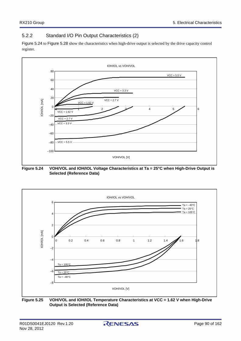
R01DS0041EJ0120 Rev.1.20 Page 90 of 162Nov 28, 2012
RX210 Group 5. Electrical Characteristics
5.2.2 Standard I/O Pin Output Characteristics (2)
Figure 5.24 to Figure 5.28 show the characteristics when high-drive output is selected by the drive capacity control
register.
Figure 5.24 VOH/VOL and IOH/IOL Voltage Characteristics at Ta = 25°C when High-Drive Output is Selected (Reference Data)
Figure 5.25 VOH/VOL and IOH/IOL Temperature Characteristics at VCC = 1.62 V when High-Drive Output is Selected (Reference Data)
VCC = 5.5 V
VCC = 3.3 V
VCC = 2.7 V
VCC = 2.7 V
VCC = 1.62 V
VCC = 1.62 V
IOH/IOL vs VOH/VOL
VOH/VOL [V]
IOH
/IOL
[mA
]
–100
–80
–60
–40
–20
0
20
40
60
80
60 1 2 3 4 5
VCC = 5.5 V
VCC = 3.3 V
IOH/IOL vs VOH/VOL
VOH/VOL [V]
IOH
/IOL
[mA
]
0 0.2 0.4 0.6 0.8 1 1.2 1.4 1.6 1.8
–8
–6
–4
–2
0
2
4
6
Ta = 105°CTa = 25°C
Ta = –40°C
Ta = 105°C
Ta = 25°C
Ta = –40°C

R01DS0041EJ0120 Rev.1.20 Page 91 of 162Nov 28, 2012
RX210 Group 5. Electrical Characteristics
Figure 5.26 VOH/VOL and IOH/IOL Temperature Characteristics at VCC = 2.7 V when High-Drive Output is Selected (Reference Data)
Figure 5.27 VOH/VOL and IOH/IOL Temperature Characteristics at VCC = 3.3 V when High-Drive Output is Selected (Reference Data)
IOH/IOL vs VOH/VOL
VOH/VOL [V]
IOH
/IOL
[mA
]
Ta = 105°C
Ta = 25°C
Ta = –40°C
Ta = 105°C
Ta = 25°C
Ta = –40°C
0 0.5 1 1.5 2 2.5 3
–30
–20
–10
0
10
20
30
IOH/IOL vs VOH/VOL
VOH/VOL [V]
IOH
/IOL
[mA
]
Ta = 105°C
Ta = 25°C
Ta = –40°C
Ta = 105°C
Ta = 25°C
Ta = –40°C
0 0.5 1 1.5 2 2.5 3 3.5
–50
–40
–30
–20
–10
0
10
20
30
40
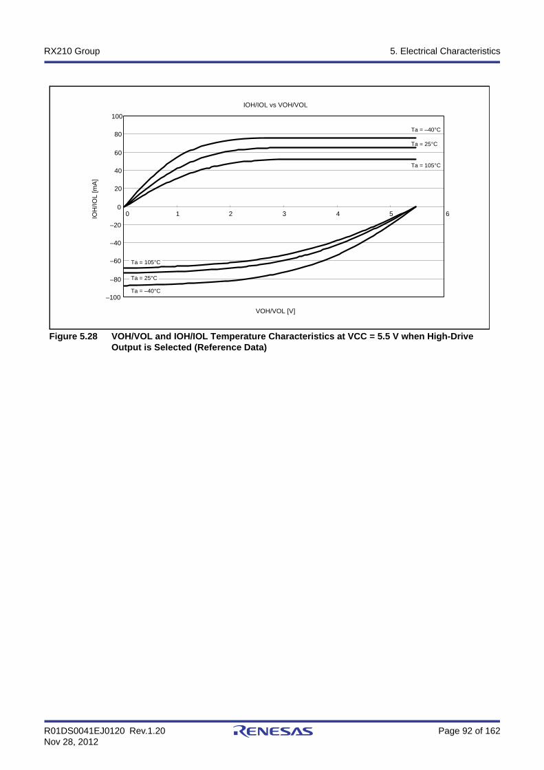
R01DS0041EJ0120 Rev.1.20 Page 92 of 162Nov 28, 2012
RX210 Group 5. Electrical Characteristics
Figure 5.28 VOH/VOL and IOH/IOL Temperature Characteristics at VCC = 5.5 V when High-Drive Output is Selected (Reference Data)
Ta = 105°C
Ta = 25°C
Ta = –40°C
Ta = –40°C
IOH/IOL vs VOH/VOL
VOH/VOL [V]
IOH
/IOL
[mA
]
0 1 2 3 4 5 6
–100
–80
–60
–40
–20
0
20
40
60
80
100
Ta = 25°C
Ta = 105°C

R01DS0041EJ0120 Rev.1.20 Page 93 of 162Nov 28, 2012
RX210 Group 5. Electrical Characteristics
5.2.3 RIIC Pin Output Characteristics
Figure 5.29 to Figure 5.32 show the output characteristics of the RIIC pin.
Figure 5.29 VOL and IOL Voltage Characteristics of RIIC Output Pin at Ta = 25°C (Reference Data)
Figure 5.30 VOL and IOL Temperature Characteristics of RIIC Output Pin at VCC = 2.7 V (Reference Data)
VCC = 5.5 V
VCC = 3.3 V
VCC = 2.7 V
IOL vs VOL [V]
VOL [V]
IOL
[mA
]
0
10
20
30
40
50
60
70
0 1 2 3 4 5 6
IOL vs VOL [V]
VOL [V]
IOL
[mA
] Ta = 105°C
Ta = 25°C
Ta = –40°C
0
5
10
15
20
25
0 0.5 1 1.5 2 2.5 3
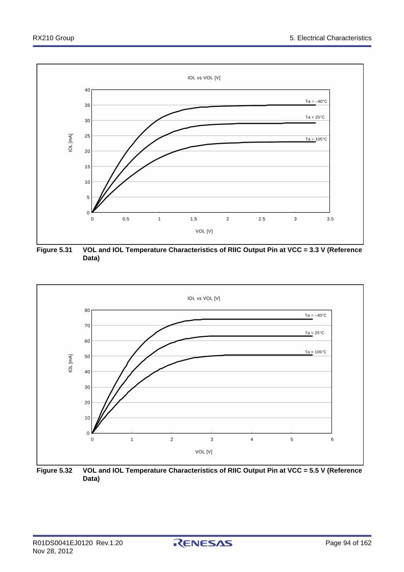
R01DS0041EJ0120 Rev.1.20 Page 94 of 162Nov 28, 2012
RX210 Group 5. Electrical Characteristics
Figure 5.31 VOL and IOL Temperature Characteristics of RIIC Output Pin at VCC = 3.3 V (Reference Data)
Figure 5.32 VOL and IOL Temperature Characteristics of RIIC Output Pin at VCC = 5.5 V (Reference Data)
Ta = 105°C
Ta = 25°C
Ta = –40°C
IOL vs VOL [V]
VOL [V]
IOL
[mA
]
0 0.5 1 1.5 2 2.5 3 3.50
5
10
15
20
25
30
35
40
Ta = 105°C
Ta = 25°C
Ta = –40°C
IOL vs VOL [V]
VOL [V]
IOL
[mA
]
0 1 2 3 4 5 60
10
20
30
40
50
60
70
80
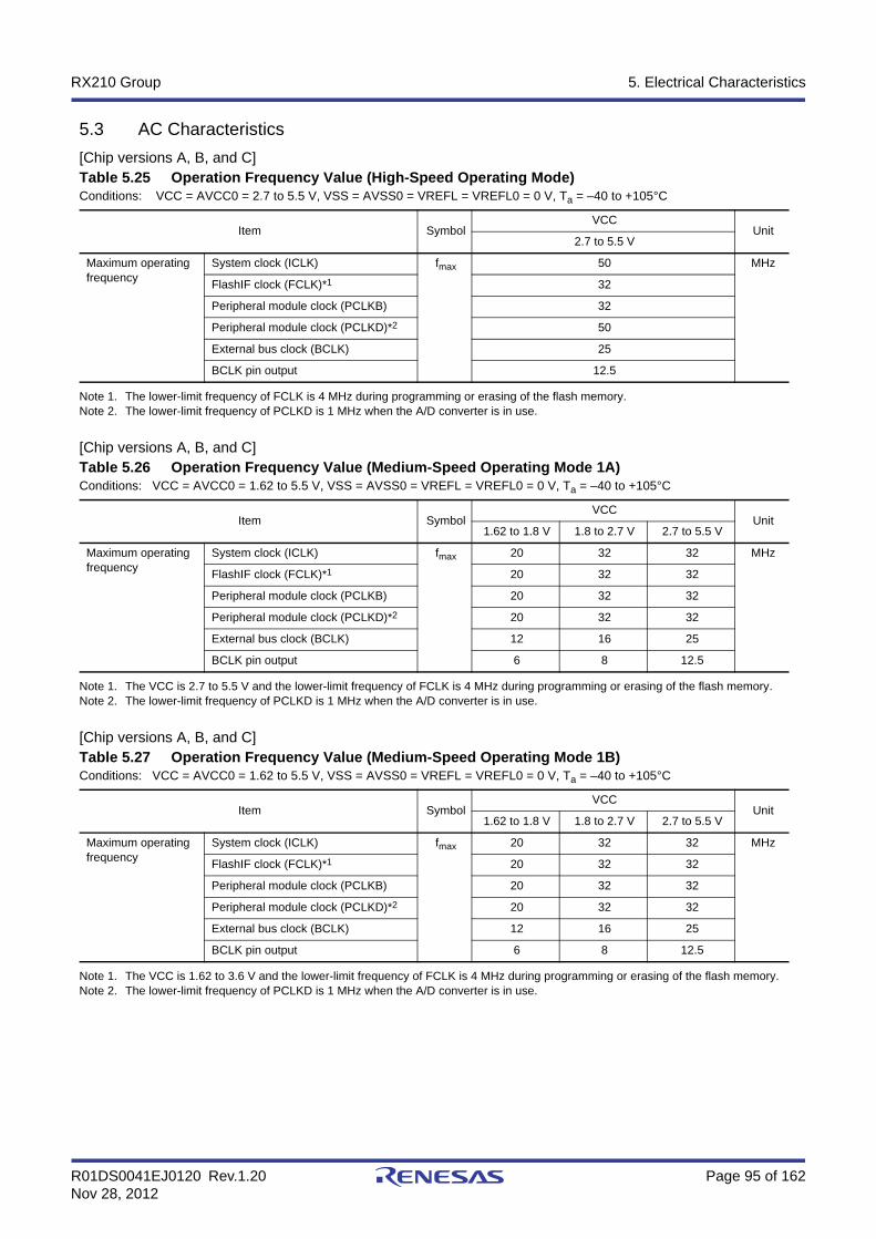
R01DS0041EJ0120 Rev.1.20 Page 95 of 162Nov 28, 2012
RX210 Group 5. Electrical Characteristics
5.3 AC Characteristics
[Chip versions A, B, and C]
Note 1. The lower-limit frequency of FCLK is 4 MHz during programming or erasing of the flash memory.Note 2. The lower-limit frequency of PCLKD is 1 MHz when the A/D converter is in use.
[Chip versions A, B, and C]
Note 1. The VCC is 2.7 to 5.5 V and the lower-limit frequency of FCLK is 4 MHz during programming or erasing of the flash memory.Note 2. The lower-limit frequency of PCLKD is 1 MHz when the A/D converter is in use.
[Chip versions A, B, and C]
Note 1. The VCC is 1.62 to 3.6 V and the lower-limit frequency of FCLK is 4 MHz during programming or erasing of the flash memory.Note 2. The lower-limit frequency of PCLKD is 1 MHz when the A/D converter is in use.
Table 5.25 Operation Frequency Value (High-Speed Operating Mode)Conditions: VCC = AVCC0 = 2.7 to 5.5 V, VSS = AVSS0 = VREFL = VREFL0 = 0 V, Ta = –40 to +105°C
Item SymbolVCC
Unit2.7 to 5.5 V
Maximum operating frequency
System clock (ICLK) fmax 50 MHz
FlashIF clock (FCLK)*1 32
Peripheral module clock (PCLKB) 32
Peripheral module clock (PCLKD)*2 50
External bus clock (BCLK) 25
BCLK pin output 12.5
Table 5.26 Operation Frequency Value (Medium-Speed Operating Mode 1A)Conditions: VCC = AVCC0 = 1.62 to 5.5 V, VSS = AVSS0 = VREFL = VREFL0 = 0 V, Ta = –40 to +105°C
Item SymbolVCC
Unit1.62 to 1.8 V 1.8 to 2.7 V 2.7 to 5.5 V
Maximum operating frequency
System clock (ICLK) fmax 20 32 32 MHz
FlashIF clock (FCLK)*1 20 32 32
Peripheral module clock (PCLKB) 20 32 32
Peripheral module clock (PCLKD)*2 20 32 32
External bus clock (BCLK) 12 16 25
BCLK pin output 6 8 12.5
Table 5.27 Operation Frequency Value (Medium-Speed Operating Mode 1B)Conditions: VCC = AVCC0 = 1.62 to 5.5 V, VSS = AVSS0 = VREFL = VREFL0 = 0 V, Ta = –40 to +105°C
Item SymbolVCC
Unit1.62 to 1.8 V 1.8 to 2.7 V 2.7 to 5.5 V
Maximum operating frequency
System clock (ICLK) fmax 20 32 32 MHz
FlashIF clock (FCLK)*1 20 32 32
Peripheral module clock (PCLKB) 20 32 32
Peripheral module clock (PCLKD)*2 20 32 32
External bus clock (BCLK) 12 16 25
BCLK pin output 6 8 12.5
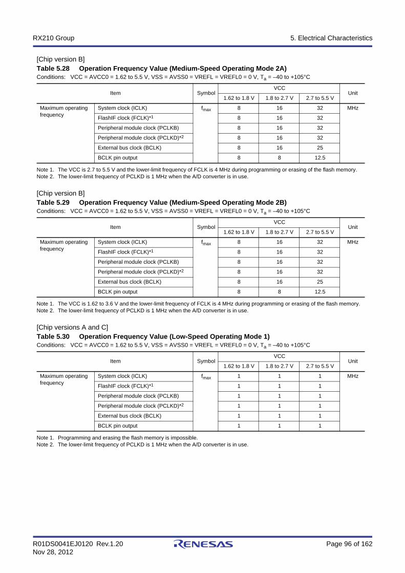
R01DS0041EJ0120 Rev.1.20 Page 96 of 162Nov 28, 2012
RX210 Group 5. Electrical Characteristics
[Chip version B]
Note 1. The VCC is 2.7 to 5.5 V and the lower-limit frequency of FCLK is 4 MHz during programming or erasing of the flash memory.Note 2. The lower-limit frequency of PCLKD is 1 MHz when the A/D converter is in use.
[Chip version B]
Note 1. The VCC is 1.62 to 3.6 V and the lower-limit frequency of FCLK is 4 MHz during programming or erasing of the flash memory.Note 2. The lower-limit frequency of PCLKD is 1 MHz when the A/D converter is in use.
[Chip versions A and C]
Note 1. Programming and erasing the flash memory is impossible.Note 2. The lower-limit frequency of PCLKD is 1 MHz when the A/D converter is in use.
Table 5.28 Operation Frequency Value (Medium-Speed Operating Mode 2A)Conditions: VCC = AVCC0 = 1.62 to 5.5 V, VSS = AVSS0 = VREFL = VREFL0 = 0 V, Ta = –40 to +105°C
Item SymbolVCC
Unit1.62 to 1.8 V 1.8 to 2.7 V 2.7 to 5.5 V
Maximum operating frequency
System clock (ICLK) fmax 8 16 32 MHz
FlashIF clock (FCLK)*1 8 16 32
Peripheral module clock (PCLKB) 8 16 32
Peripheral module clock (PCLKD)*2 8 16 32
External bus clock (BCLK) 8 16 25
BCLK pin output 8 8 12.5
Table 5.29 Operation Frequency Value (Medium-Speed Operating Mode 2B)Conditions: VCC = AVCC0 = 1.62 to 5.5 V, VSS = AVSS0 = VREFL = VREFL0 = 0 V, Ta = –40 to +105°C
Item SymbolVCC
Unit1.62 to 1.8 V 1.8 to 2.7 V 2.7 to 5.5 V
Maximum operating frequency
System clock (ICLK) fmax 8 16 32 MHz
FlashIF clock (FCLK)*1 8 16 32
Peripheral module clock (PCLKB) 8 16 32
Peripheral module clock (PCLKD)*2 8 16 32
External bus clock (BCLK) 8 16 25
BCLK pin output 8 8 12.5
Table 5.30 Operation Frequency Value (Low-Speed Operating Mode 1)Conditions: VCC = AVCC0 = 1.62 to 5.5 V, VSS = AVSS0 = VREFL = VREFL0 = 0 V, Ta = –40 to +105°C
Item SymbolVCC
Unit1.62 to 1.8 V 1.8 to 2.7 V 2.7 to 5.5 V
Maximum operating frequency
System clock (ICLK) fmax 1 1 1 MHz
FlashIF clock (FCLK)*1 1 1 1
Peripheral module clock (PCLKB) 1 1 1
Peripheral module clock (PCLKD)*2 1 1 1
External bus clock (BCLK) 1 1 1
BCLK pin output 1 1 1
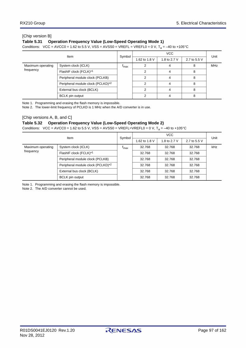
R01DS0041EJ0120 Rev.1.20 Page 97 of 162Nov 28, 2012
RX210 Group 5. Electrical Characteristics
[Chip version B]
Note 1. Programming and erasing the flash memory is impossible.Note 2. The lower-limit frequency of PCLKD is 1 MHz when the A/D converter is in use.
[Chip versions A, B, and C]
Note 1. Programming and erasing the flash memory is impossible.Note 2. The A/D converter cannot be used.
Table 5.31 Operation Frequency Value (Low-Speed Operating Mode 1)Conditions: VCC = AVCC0 = 1.62 to 5.5 V, VSS = AVSS0 = VREFL = VREFL0 = 0 V, Ta = –40 to +105°C
Item SymbolVCC
Unit1.62 to 1.8 V 1.8 to 2.7 V 2.7 to 5.5 V
Maximum operating frequency
System clock (ICLK) fmax 2 4 8 MHz
FlashIF clock (FCLK)*1 2 4 8
Peripheral module clock (PCLKB) 2 4 8
Peripheral module clock (PCLKD)*2 2 4 8
External bus clock (BCLK) 2 4 8
BCLK pin output 2 4 8
Table 5.32 Operation Frequency Value (Low-Speed Operating Mode 2)Conditions: VCC = AVCC0 = 1.62 to 5.5 V, VSS = AVSS0 = VREFL=VREFL0 = 0 V, Ta = –40 to +105°C
Item SymbolVCC
Unit1.62 to 1.8 V 1.8 to 2.7 V 2.7 to 5.5 V
Maximum operating frequency
System clock (ICLK) fmax 32.768 32.768 32.768 kHz
FlashIF clock (FCLK)*1 32.768 32.768 32.768
Peripheral module clock (PCLKB) 32.768 32.768 32.768
Peripheral module clock (PCLKD)*2 32.768 32.768 32.768
External bus clock (BCLK) 32.768 32.768 32.768
BCLK pin output 32.768 32.768 32.768

R01DS0041EJ0120 Rev.1.20 Page 98 of 162Nov 28, 2012
RX210 Group 5. Electrical Characteristics
5.3.1 Clock Timing
Note 1. When the EXTAL external clock input is used with divided by 1 (SCKCR.BCK[3:0] bits = 0000b and BCKCR.BCLKDIV bit = 0) to output from the BCLK pin, the above should be satisfied with a duty cycle of 45 to 55%.
Note 1. When the EXTAL external clock input is used with divided by 1 (SCKCR.BCK[3:0] bits = 0000b and BCKCR.BCLKDIV bit = 0) to output from the BCLK pin, the above should be satisfied with a duty cycle of 45 to 55%.
Note: • Set high driving ability for the output port pin to be used for the BCLK pin function.Note 1. When the EXTAL external clock input is used with divided by 1 (SCKCR.BCK[3:0] bits = 0000b and BCKCR.BCLKDIV bit = 0) to
output from the BCLK pin, the above should be satisfied with a duty cycle of 45 to 55%.
Table 5.33 BCLK Timing (1)Conditions: VCC = AVCC0 = 2.7 to 5.5 V, VSS = AVSS0 = VREFL = VREFL0 = 0 V,
fBCLK = up to 25 MHz (BCLK pin output frequency = up to 12.5 MHz), Ta = –40 to +105°C
Item Symbol Min. Typ. Max. Unit Test Conditions
BCLK pin output cycle time tBcyc 80 — — ns Figure 5.33
BCLK pin output high pulse width*1 tCH 20 — — ns
BCLK pin output low pulse width*1 tCL 20 — — ns
BCLK pin output rising time tCr — — 15 ns
BCLK pin output falling time tCf — — 15 ns
Table 5.34 BCLK Timing (2)Conditions: VCC = AVCC0 = 1.8 to 2.7 V, VSS = AVSS0 = VREFL = VREFL0 = 0 V,
fBCLK = up to 16 MHz (BCLK pin output frequency= up to 8 MHz), Ta = –40 to +105°C
Item Symbol Min. Typ. Max. Unit Test Conditions
BCLK pin output cycle time tBcyc 125 — — ns Figure 5.33
BCLK pin output high pulse width*1 tCH 30 — — ns
BCLK pin output low pulse width*1 tCL 30 — — ns
BCLK pin output rising time tCr — — 25 ns
BCLK pin output falling time tCf — — 25 ns
Table 5.35 BCLK Timing (3)Conditions: VCC = AVCC0 = 1.62 to 1.8 V, VSS = AVSS0 = VREFL=VREFL0 = 0 V,
fBCLK = up to 12 MHz (BCLK pin output frequency = up to 6 MHz), Ta = –40 to +105°C
Item Symbol Min. Typ. Max. Unit Test Conditions
BCLK pin output cycle time tBcyc 166.6 — — ns Figure 5.33
BCLK pin output high pulse width*1 tCH 42 — — ns
BCLK pin output low pulse width*1 tCL 42 — — ns
BCLK pin output rising time tCr — — 35 ns
BCLK pin output falling time tCf — — 35 ns

R01DS0041EJ0120 Rev.1.20 Page 99 of 162Nov 28, 2012
RX210 Group 5. Electrical Characteristics
Note 1. The time interval from the time P36 and P37 are configured for input and the main clock oscillator stopping bit (MOSCCR.MOSTP) is set to 0 (operating) until the clock becomes available.
Table 5.36 Clock TimingConditions: VCC = AVCC0 = 1.62 to 5.5 V, VSS = AVSS0 = VREFL = VREFL0 = 0 V, Ta = –40 to +105°C
Item Symbol Min. Typ. Max. UnitTest
Conditions
EXTAL external clock input cycle time tEXcyc 50 — — ns Figure 5.34
EXTAL external clock input high pulse width tEXH 20 — — ns
EXTAL external clock input low pulse width tEXL 20 — — ns
EXTAL external clock rising time tEXr — — 5 ns
EXTAL external clock falling time tEXf — — 5 ns
EXTAL external clock input wait time*1 tEXWT 1 — — ms
Main clock oscillator oscillation frequency*2 fMAIN 1 — 20 MHz
Main clock oscillation stabilization time (crystal)*2 tMAINOSC — 3 — ms Figure 5.35
Main clock oscillation stabilization time (ceramic resonator)*2 tMAINOSC — 50 µs
Main clock oscillation stabilization wait time (crystal)*2 tMAINOSCWT — 6 — ms
Main clock oscillation stabilization wait time (ceramic resonator)*2 tMAINOSCWT — 100 µs
LOCO clock cycle time tcyc 7.27 8 8.89 µs
LOCO clock oscillation frequency fLOCO 112.5 125 137.5 kHz
LOCO clock oscillation stabilization wait time tLOCOWT — — 20 µs Figure 5.36
HOCO clock oscillation frequency fHOCO 31.680 32 32.320 MHz Ta = 0 to 50°C
36.495 36.864 37.233
39.600 40 40.400
49.500 50 50.500
31.520 32 32.480 Ta = -40 to 105°C
36.311 36.864 37.417
39.400 40 40.600
49.250 50 50.750
HOCO clock oscillation stabilization time 1 tHOCO1 — — 300 µs Figure 5.37
HOCO clock oscillation stabilization time 2 tHOCO2 — — 175 µs Figure 5.38
HOCO clock oscillation stabilization wait time tHOCOWT — — 350 µs Figure 5.38
HOCO clock power supply stabilization time tHOCOP — — 350 µs Figure 5.39
PLL input frequency fPLLIN 4 — 12.5 MHz
PLL circuit oscillation frequency fPLL 50 — 100 MHz
PLL clock oscillation stabilization time PLL operation started after main clock oscillation has settled
tPLL1 — — 500 µs Figure 5.40
PLL clock oscillation stabilization wait time tPLLWT1 1.5 — — ms
PLL clock oscillation stabilization time*4 PLL operation started before main clock oscillation has settled
tPLL2 — 3.5*3 — ms Figure 5.41
PLL clock oscillation stabilization wait time*4
tPLLWT2 — 7 — ms
PLL clock power supply stabilization time (for chip version B only) tPLLPW — — 30 µs Figure 5.42
Sub-clock oscillator oscillation frequency fSUB — 32.768 — kHz
Sub-clock oscillation stabilization time*5 tSUBOSC 2 — — s Figure 5.43
Sub-clock oscillation stabilization wait time*5 tSUBOSCWT 4 — — s

R01DS0041EJ0120 Rev.1.20 Page 100 of 162Nov 28, 2012
RX210 Group 5. Electrical Characteristics
Note 2. When specifying the main clock oscillator stabilization time, load MOSCWTCR register with a stabilization time value that is greater than the resonator-vendor-recommended value. When determining the main lock oscillation stabilization wait time, allow an adequate margin (2 times is recommended) for the main clock oscillation stabilization time.Start using the main clock in the main clock oscillation stabilization wait time (tMAINOSCWT) after setting up the main clock oscillator for operation with the MOSCCR.MOSTP bit.The indicated value is a reference value that is measured for an 8 MHz resonator.
Note 3. Sum of the main clock oscillation stabilization time and the PLL oscillation stabilization time.Note 4. The indicated value is a reference value that is measured for an 8 MHz resonator.Note 5. When specifying the sub-clock oscillation stabilization time, load SOSCWTCR register with the resonator-vendor-recommended
stabilization time value minus 2 seconds. When determining the sub-clock oscillation stabilization wait time, allow an adequate margin (2 times is recommended) for the sub-clock oscillation stabilization time. Start using the sub-clock in the sub-clock oscillation stabilization wait time (tSUBOSCWT) after setting up the sub-clock oscillator for operation with the SOSCCR.SOSTP or RCR3.RTCEN bit.
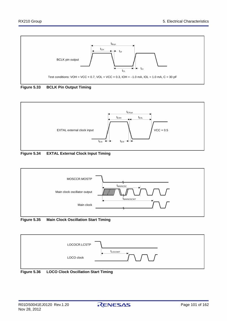
R01DS0041EJ0120 Rev.1.20 Page 101 of 162Nov 28, 2012
RX210 Group 5. Electrical Characteristics
Figure 5.33 BCLK Pin Output Timing
Figure 5.34 EXTAL External Clock Input Timing
Figure 5.35 Main Clock Oscillation Start Timing
Figure 5.36 LOCO Clock Oscillation Start Timing
tCftCH
tBcyc
tCrtCL
BCLK pin output
Test conditions: VOH = VCC × 0.7, VOL = VCC × 0.3, IOH = 1.0 mA, IOL = 1.0 mA, C = 30 pF
tEXH
tEXcyc
EXTAL external clock input VCC × 0.5
tEXL
tEXr tEXf
Main clock oscillator output
MOSCCR.MOSTP
tMAINOSC
Main clock
tMAINOSCWT
LOCO clock
LOCOCR.LCSTP
tLOCOWT

R01DS0041EJ0120 Rev.1.20 Page 102 of 162Nov 28, 2012
RX210 Group 5. Electrical Characteristics
Figure 5.37 HOCO Clock Oscillation Start Timing (After Reset is Canceled by Setting the OFS1.HOCOEN Bit to 0)
Figure 5.38 HOCO Clock Oscillation Start Timing (Oscillation is Started by Setting the HOCOCR.HCSTP Bit)
Figure 5.39 HOCO Power Control Timing
RES#
Internal reset
HOCO clock
OFS1.HOCOEN
tHOCO1
tRESWT
HOCOCR.HCSTP
tHOCOWT
tHOCO2
HOCO clock
HOCO clock output
Internal power supply for HOCO
HOCOPCR.HOCOPCNT
tHOCOP
HOCOCR.HCSTP
R01DS0041EJ0120 Rev.1.20 Page 103 of 162Nov 28, 2012
RX210 Group 5. Electrical Characteristics
Figure 5.40 PLL Clock Oscillation Start Timing (PLL is Operated after Main Clock Oscillation Has Settled)
Figure 5.41 PLL Clock Oscillation Start Timing (PLL is Operated before Main Clock Oscillation Has Settled)
Figure 5.42 PLL Power Control Timing
PLLCR2.PLLEN
PLL clock
MOSCCR.MOSTP
tMAINOSC
Main clock oscillator output
PLL circuit output
tPLL1
tPLLWT1
MOSCCR.MOSTP
PLL circuit output
PLLCR2.PLLEN
tPLL2
tMAINOSC
Main clock oscillator output
PLL clock
tPLLWT2
Internal power supply for PLL
PLLPCR.PLLPCNT
tPLLPW
PLLCR2.PLLEN
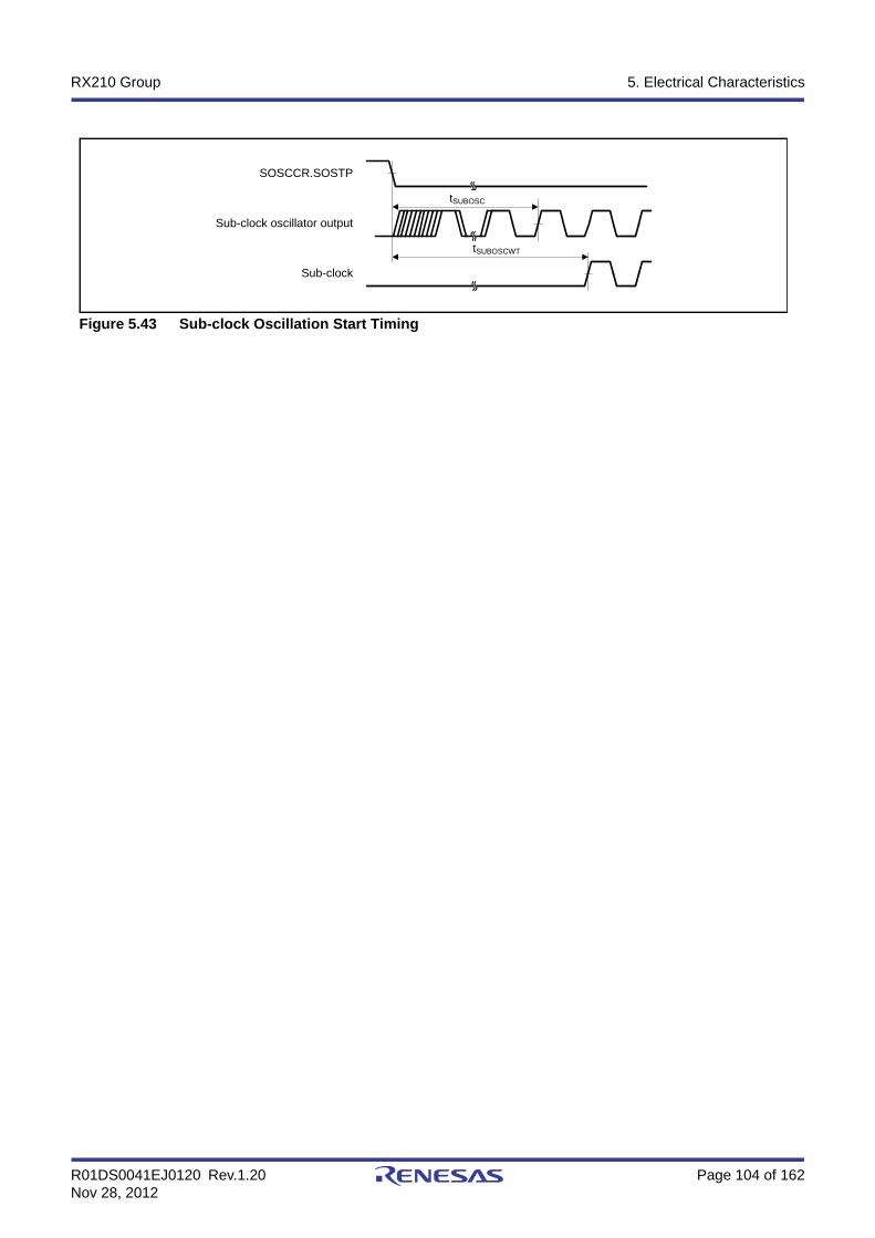
R01DS0041EJ0120 Rev.1.20 Page 104 of 162Nov 28, 2012
RX210 Group 5. Electrical Characteristics
Figure 5.43 Sub-clock Oscillation Start Timing
Sub-clock oscillator output
SOSCCR.SOSTP
tSUBOSC
Sub-clock
tSUBOSCWT

R01DS0041EJ0120 Rev.1.20 Page 105 of 162Nov 28, 2012
RX210 Group 5. Electrical Characteristics
5.3.2 Reset Timing
Figure 5.44 Reset Input Timing at Power-On
Figure 5.45 Reset Input Timing
Table 5.37 Reset TimingConditions: VCC = AVCC0 = 1.62 to 5.5 V, VSS = AVSS0 = VREFL = VREFL0 = 0 V, Ta = –40 to +105°C
Item Symbol Min. Typ. Max. UnitTest
Conditions
RES# pulse width
Power-on tRESWP 8 — — ms Figure 5.44
Deep software standby mode tRESWD 8 — — ms Figure 5.45
Software standby mode, low-speed operating modes 1 and 2
tRESWS 1 — — ms
Programming or erasure of the ROM or E2 DataFlash memory or blank checking of the E2 DataFlash memory
tRESWF 200 — — µs
Other than above tRESW 200 — — µs
Wait time after RES# cancellation tRESWT — — 912 µs Figure 5.44
Internal reset time(independent watchdog timer reset, watchdog timer reset, software reset)
tRESW2 — — 1.4 ms
VCC
RES#
tRESWP
Internal reset
tRESWT
1.55 V
RES#
Internal reset
tRESWT
tRESWD, tRESWS, tRESWF, tRESW

R01DS0041EJ0120 Rev.1.20 Page 106 of 162Nov 28, 2012
RX210 Group 5. Electrical Characteristics
5.3.3 Timing of Recovery from Low Power Consumption Modes
[Chip versions A and C]
Note 1. The recovery time varies depending on the state of each oscillator when the WAIT instruction is executed. The recovery time when multiple oscillators are operating varies depending on the operating state of the oscillators that are not selected as the system clock source, and depends on the time set in the wait control registers corresponding to the oscillators.
Note 2. The indicated value is measured for an 8 MHz crystal resonator.Note 3. When RCR3.RTCEN = 1, the time will be the time set in the SOSCWTCR register minus 2 s.Note 4. When RCR3.RTCEN = 1, the time will be the time set in the SOSCWTCR register minus 2 s and plus 31.25 ms.
Table 5.38 Timing of Recovery from Low Power Consumption ModesConditions: VCC = AVCC0 = 1.62 to 5.5 V, VSS = AVSS0 = VREFL = VREFL0 = 0 V, Ta = –40 to +105°C
Item Symbol Min. Typ. Max. UnitTest
Conditions
Recovery time after cancellation of software standby mode (flash memory, HOCO power supplied)(SOFTCUT[2:0] bits = 000b)*1
Crystal resonator connected to main clock oscillator*2
Main clock oscillator operating
tSBYMC — 3 — ms Figure 5.46
Main clock oscillator and PLL circuit operating
tSBYPC — 3.5 — ms
External clock input to main clock oscillator
Main clock oscillator operating
tSBYEX 10 — — µs
Main clock oscillator and PLL circuit operating
tSBYPE 0.5 — — ms
Sub-clock oscillator operating tSBYSC 2*3 — — s
HOCO clock oscillator operating tSBYHO — — 500 µs
LOCO clock oscillator operating tSBYLO — — 90 µs
Recovery time after cancellation of software standby mode (flash memory power supplied, HOCO power not supplied)(SOFTCUT[2:0] bits = 110b)*1
Crystal resonator connected to main clock oscillator*2
Main clock oscillator operating
tSBYMC — 3 — ms Figure 5.46
Main clock oscillator and PLL circuit operating
tSBYPC — 3.5 — ms
External clock input to main clock oscillator
Main clock oscillator operating
tSBYEX 40 — — µs
Main clock oscillator and PLL circuit operating
tSBYPE 0.5 — — ms
Sub-clock oscillator operating tSBYSC 2*3 — — s
HOCO clock oscillator operating tSBYHO — — 1.2 ms
LOCO clock oscillator operating tSBYLO — — 90 µs
Recovery time after cancellation of software standby mode (flash memory, HOCO power not supplied)(SOFTCUT[2:0] bits = 111b)*1
Crystal resonator connected to main clock oscillator*2
Main clock oscillator operating
tSBYMC — 3 — ms Figure 5.46
Main clock oscillator and PLL circuit operating
tSBYPC — 3.5 — ms
External clock input to main clock oscillator
Main clock oscillator operating
tSBYEX 100 — — µs
Main clock oscillator and PLL circuit operating
tSBYPE 0.5 — — ms
Sub-clock oscillator operating tSBYSC 2*4 — — s
HOCO clock oscillator operating tSBYHO — — 1.2 ms
LOCO clock oscillator operating tSBYLO — — 10 ms
Recovery time after cancellation of deep software standby mode tDSBY — — 8 ms Figure 5.47
Wait time after cancellation of deep software standby mode tDSBYWT — — 0.8 ms
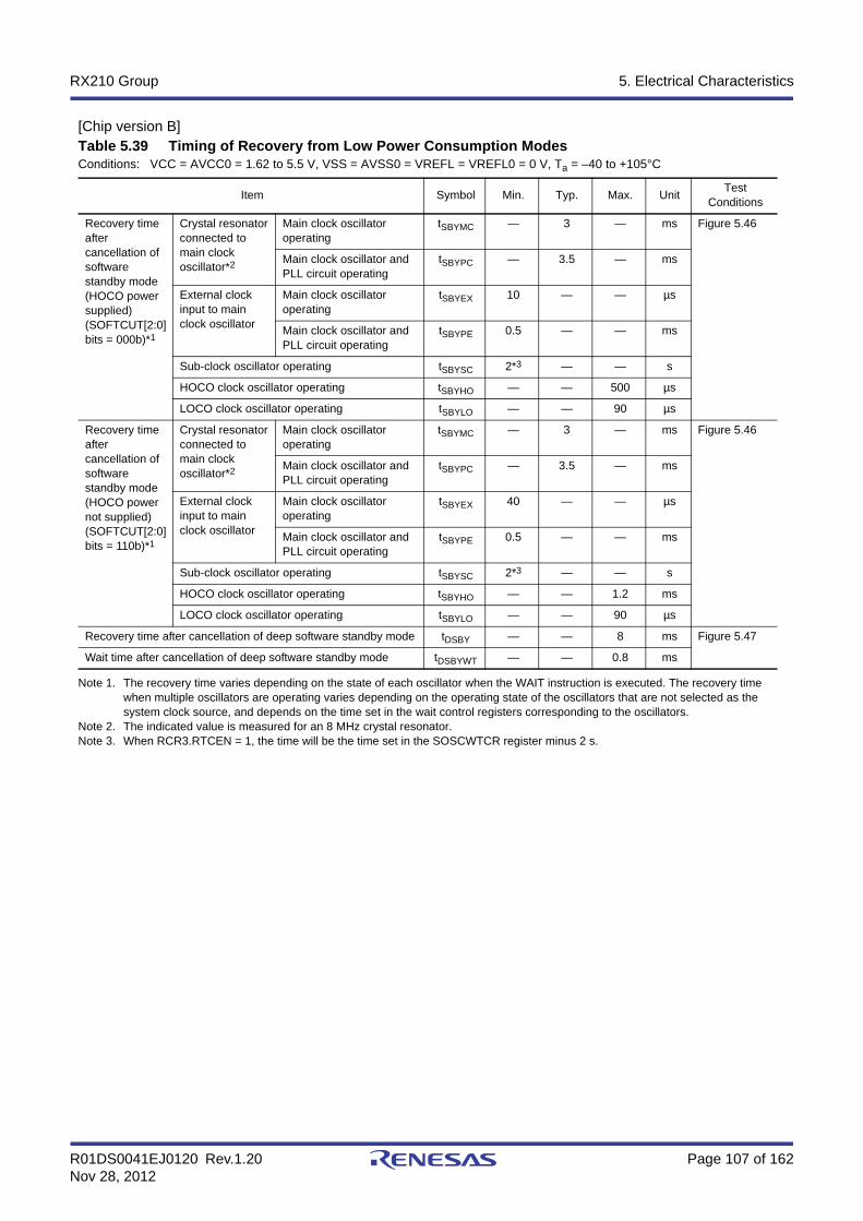
R01DS0041EJ0120 Rev.1.20 Page 107 of 162Nov 28, 2012
RX210 Group 5. Electrical Characteristics
[Chip version B]
Note 1. The recovery time varies depending on the state of each oscillator when the WAIT instruction is executed. The recovery time when multiple oscillators are operating varies depending on the operating state of the oscillators that are not selected as the system clock source, and depends on the time set in the wait control registers corresponding to the oscillators.
Note 2. The indicated value is measured for an 8 MHz crystal resonator.Note 3. When RCR3.RTCEN = 1, the time will be the time set in the SOSCWTCR register minus 2 s.
Table 5.39 Timing of Recovery from Low Power Consumption ModesConditions: VCC = AVCC0 = 1.62 to 5.5 V, VSS = AVSS0 = VREFL = VREFL0 = 0 V, Ta = –40 to +105°C
Item Symbol Min. Typ. Max. UnitTest
Conditions
Recovery time after cancellation of software standby mode (HOCO power supplied)(SOFTCUT[2:0] bits = 000b)*1
Crystal resonator connected to main clock oscillator*2
Main clock oscillator operating
tSBYMC — 3 — ms Figure 5.46
Main clock oscillator and PLL circuit operating
tSBYPC — 3.5 — ms
External clock input to main clock oscillator
Main clock oscillator operating
tSBYEX 10 — — µs
Main clock oscillator and PLL circuit operating
tSBYPE 0.5 — — ms
Sub-clock oscillator operating tSBYSC 2*3 — — s
HOCO clock oscillator operating tSBYHO — — 500 µs
LOCO clock oscillator operating tSBYLO — — 90 µs
Recovery time after cancellation of software standby mode (HOCO power not supplied)(SOFTCUT[2:0] bits = 110b)*1
Crystal resonator connected to main clock oscillator*2
Main clock oscillator operating
tSBYMC — 3 — ms Figure 5.46
Main clock oscillator and PLL circuit operating
tSBYPC — 3.5 — ms
External clock input to main clock oscillator
Main clock oscillator operating
tSBYEX 40 — — µs
Main clock oscillator and PLL circuit operating
tSBYPE 0.5 — — ms
Sub-clock oscillator operating tSBYSC 2*3 — — s
HOCO clock oscillator operating tSBYHO — — 1.2 ms
LOCO clock oscillator operating tSBYLO — — 90 µs
Recovery time after cancellation of deep software standby mode tDSBY — — 8 ms Figure 5.47
Wait time after cancellation of deep software standby mode tDSBYWT — — 0.8 ms
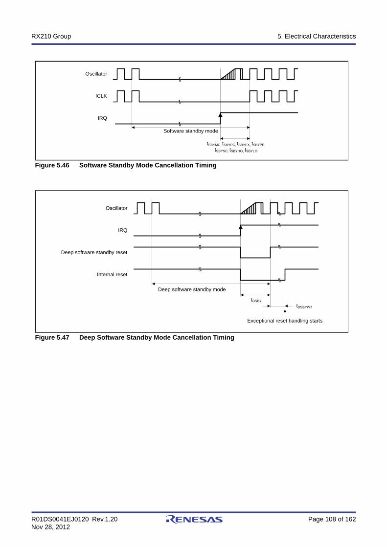
R01DS0041EJ0120 Rev.1.20 Page 108 of 162Nov 28, 2012
RX210 Group 5. Electrical Characteristics
Figure 5.46 Software Standby Mode Cancellation Timing
Figure 5.47 Deep Software Standby Mode Cancellation Timing
Oscillator
ICLK
IRQ
Software standby mode
tSBYMC, tSBYPC, tSBYEX, tSBYPE,
tSBYSC, tSBYHO, tSBYLO
Oscillator
IRQ
Internal reset
Exceptional reset handling starts
Deep software standby mode
Deep software standby reset
tDSBY
tDSBYWT
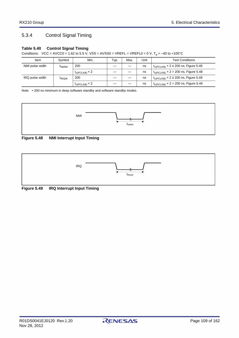
R01DS0041EJ0120 Rev.1.20 Page 109 of 162Nov 28, 2012
RX210 Group 5. Electrical Characteristics
5.3.4 Control Signal Timing
Note: • 200 ns minimum in deep software standby and software standby modes.
Figure 5.48 NMI Interrupt Input Timing
Figure 5.49 IRQ Interrupt Input Timing
Table 5.40 Control Signal TimingConditions: VCC = AVCC0 = 1.62 to 5.5 V, VSS = AVSS0 = VREFL = VREFL0 = 0 V, Ta = –40 to +105°C
Item Symbol Min. Typ. Max. Unit Test Conditions
NMI pulse width tNMIW 200 — — ns tc(PCLKB) × 2 ≤ 200 ns, Figure 5.48
tc(PCLKB) × 2 — — ns tc(PCLKB) × 2 > 200 ns, Figure 5.48
IRQ pulse width tIRQW 200 — — ns tc(PCLKB) × 2 ≤ 200 ns, Figure 5.49
tc(PCLKB) × 2 — — ns tc(PCLKB) × 2 > 200 ns, Figure 5.49
NMI
tNMIW
IRQ
tIRQW

R01DS0041EJ0120 Rev.1.20 Page 110 of 162Nov 28, 2012
RX210 Group 5. Electrical Characteristics
5.3.5 Bus Timing
Table 5.41 Bus Timing (1)Conditions: VCC = AVCC0 = 2.7 to 5.5 V, VSS = AVSS0 = VREFL = VREFL0 = 0 V, (fBCLK output = up to 12.5 MHz),
Ta = –40 to +105°C, VOH = VCC × 0.5, VOL = VCC × 0.5, IOH = –1.0 mA, IOL = 1.0 mA, CL = 30 pFWhen normal output is selected by the drive capacity register
Item Symbol Min. Max. Unit Test Conditions
Address delay time tAD — 60 ns Figure 5.50 to Figure 5.53
Byte control delay time tBCD — 60 ns
CS# delay time tCSD — 60 ns
RD# delay time tRSD — 60 ns
Read data setup time tRDS 40 — ns
Read data hold time tRDH 0 — ns
WR# delay time tWRD — 60 ns
Write data delay time tWDD — 60 ns
Write data hold time tWDH 0 — ns
WAIT# setup time tWTS 40 — ns Figure 5.54
WAIT# hold time tWTH 0 — ns
Table 5.42 Bus Timing (2)Conditions: VCC = AVCC0 = 1.8 to 2.7 V, VSS = AVSS0 = VREFL = VREFL0 = 0 V, (fBCLK output = up to 8 MHz),
Ta = –40 to +105°C, VOH = VCC × 0.5, VOL = VCC × 0.5, IOH = –1.0 mA, IOL = 1.0 mA, CL = 30 pFWhen normal output is selected by the drive capacity register
Item Symbol Min. Max. Unit Test Conditions
Address delay time tAD — 90 ns Figure 5.50 to Figure 5.53
Byte control delay time tBCD — 90 ns
CS# delay time tCSD — 90 ns
RD# delay time tRSD — 90 ns
Read data setup time tRDS 60 — ns
Read data hold time tRDH 0 — ns
WR# delay time tWRD — 90 ns
Write data delay time tWDD — 90 ns
Write data hold time tWDH 0 — ns
WAIT# setup time tWTS 60 — ns Figure 5.54
WAIT# hold time tWTH 0 — ns
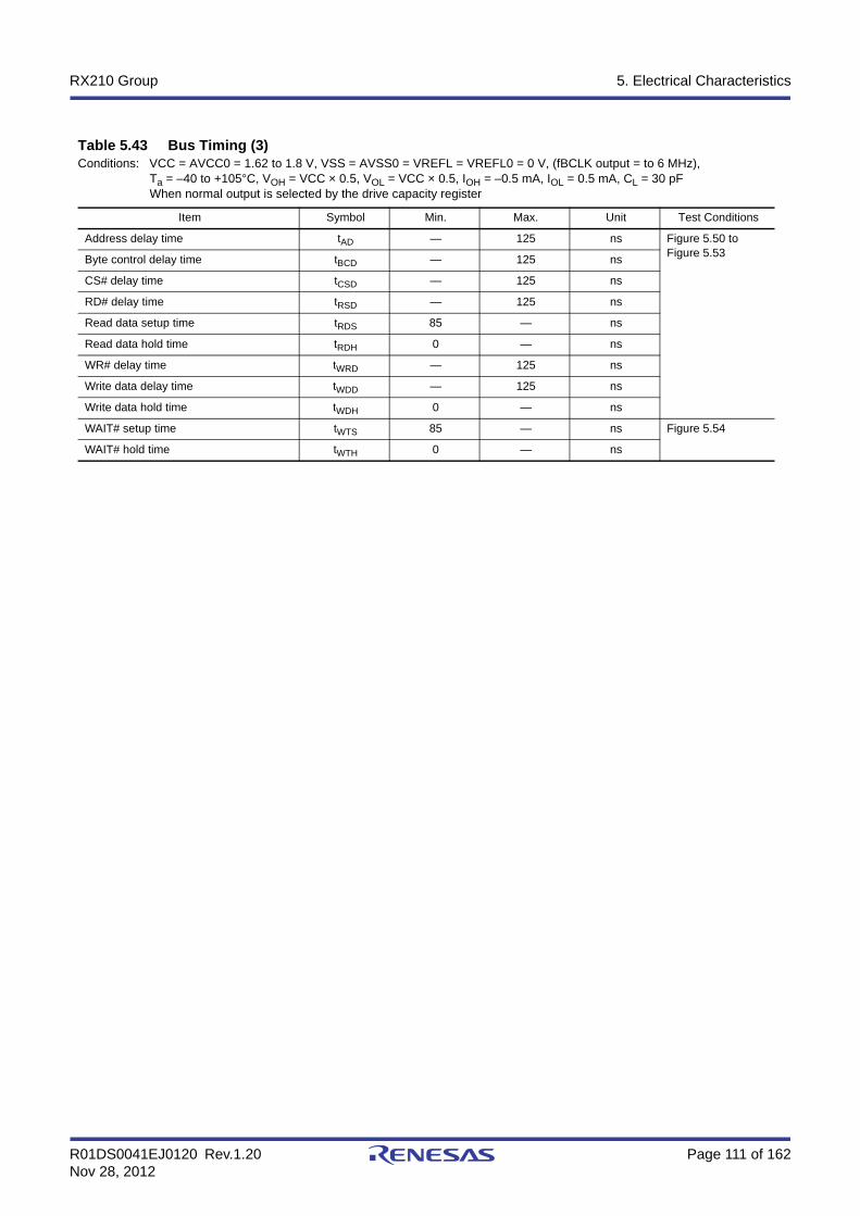
R01DS0041EJ0120 Rev.1.20 Page 111 of 162Nov 28, 2012
RX210 Group 5. Electrical Characteristics
Table 5.43 Bus Timing (3)Conditions: VCC = AVCC0 = 1.62 to 1.8 V, VSS = AVSS0 = VREFL = VREFL0 = 0 V, (fBCLK output = to 6 MHz),
Ta = –40 to +105°C, VOH = VCC × 0.5, VOL = VCC × 0.5, IOH = –0.5 mA, IOL = 0.5 mA, CL = 30 pFWhen normal output is selected by the drive capacity register
Item Symbol Min. Max. Unit Test Conditions
Address delay time tAD — 125 ns Figure 5.50 to Figure 5.53
Byte control delay time tBCD — 125 ns
CS# delay time tCSD — 125 ns
RD# delay time tRSD — 125 ns
Read data setup time tRDS 85 — ns
Read data hold time tRDH 0 — ns
WR# delay time tWRD — 125 ns
Write data delay time tWDD — 125 ns
Write data hold time tWDH 0 — ns
WAIT# setup time tWTS 85 — ns Figure 5.54
WAIT# hold time tWTH 0 — ns
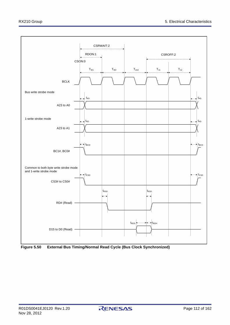
R01DS0041EJ0120 Rev.1.20 Page 112 of 162Nov 28, 2012
RX210 Group 5. Electrical Characteristics
Figure 5.50 External Bus Timing/Normal Read Cycle (Bus Clock Synchronized)
A23 to A1
CS3# to CS0#
tAD
BCLK
A23 to A0
D15 to D0 (Read)
Bus write strobe mode
1-write strobe mode
BC1#, BC0#
Common to both byte write strobe mode and 1-write strobe mode
tBCD
tCSD
RD# (Read)
tRSD tRSD
tAD
tRDHtRDS
tAD
tAD
TW1 TW2 Tend Tn1 Tn2
RDON:1
CSRWAIT:2
CSROFF:2
CSON:0
tBCD
tCSD

R01DS0041EJ0120 Rev.1.20 Page 113 of 162Nov 28, 2012
RX210 Group 5. Electrical Characteristics
Figure 5.51 External Bus Timing/Normal Write Cycle (Bus Clock Synchronized)
A23 to A1
CS3# to CS0#
tAD
BCLK
A23 to A0
Byte write strobe mode
1-write strobe mode
BC1#, BC0#
Common to both byte write strobe mode and 1-write strobe mode
tBCD
tCSD
tAD
tAD
tAD
D15 to D0 (Write)
WR1#, WR0#, WR# (Write)
tWRD tWRD
tWDH
tWDD
TW1 TW2 Tend Tn1 Tn2
WRON:1WDON:1*1
CSWWAIT:2
WDOFF:1*1CSON:0
Note 1. Set the values of WDON and WDOFF to 1 or greater.
tBCD
tCSD
CSWOFF:2
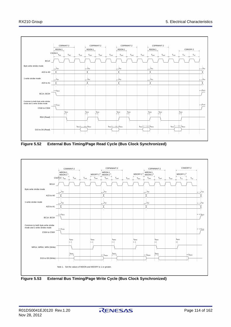
R01DS0041EJ0120 Rev.1.20 Page 114 of 162Nov 28, 2012
RX210 Group 5. Electrical Characteristics
Figure 5.52 External Bus Timing/Page Read Cycle (Bus Clock Synchronized)
Figure 5.53 External Bus Timing/Page Write Cycle (Bus Clock Synchronized)
A23 to A1
CS3# to CS0#
tAD
BCLK
A23 to A0
D15 to D0 (Read)
Byte write strobe mode
1-write strobe mode
BC1#, BC0#
Common to both byte write strobe mode and 1-write strobe mode
tBCD
tCSD
RD# (Read)
tRSD tRSD
tRDHtRDS
tAD
TW1 TW2 Tend Tpw1 Tpw2
tAD tAD
tRSD tRSD
tRDHtRDS
tRSD tRSD
tRDHtRDS
Tend Tpw1 Tpw2 Tend Tn1 Tn2
tAD tAD tAD tAD
RDON:1
CSRWAIT:2
CSROFF:2
tRSD tRSD
tRDHtRDS
tAD
tAD
CSPRWAIT:2
Tpw1 Tpw2 Tend
RDON:1
CSPRWAIT:2
RDON:1
CSPRWAIT:2
RDON:1
CSON:0
tBCD
tCSD
A23 to A1
CS3# to CS0#
tAD
BCLK
A23 to A0
Byte write strobe mode
1-write strobe mode
BC1#, BC0#
Common to both byte write strobe mode and 1-write strobe mode
tBCD
tCSD
tAD
TW1
D15 to D0 (Write)
WR1#, WR0#, WR# (Write)
tWRD tWRD
tWDH
tWDD
TW2 Tend Tpw1 Tpw2
tAD tAD
tWRD tWRD
tWDH
tWDD
tWRD tWRD
tWDHtWDD
Tdw1 Tend Tpw1 Tpw2 Tend Tn1 Tn2Tdw1
tAD tAD tAD tAD
WRON:1WDON:1*1
CSWWAIT:2 CSPWWAIT:2
WDOFF:1*1
CSPWWAIT:2
WDOFF:1*1 WDOFF:1*1
CSON:0
WRON:1WDON:1*1
WRON:1WDON:1*1
Note 1. Set the values of WDON and WDOFF to 1 or greater.
tBCD
tCSD
CSWOFF:2

R01DS0041EJ0120 Rev.1.20 Page 115 of 162Nov 28, 2012
RX210 Group 5. Electrical Characteristics
Figure 5.54 External Bus Timing/External Wait Control
tWTS tWTH tWTS tWTH
CSRWAIT:3CSWWAIT:3
BCLK
A23 to A0
CS3# to CS0#
RD# (Read)
WR# (Write)
WAIT#
TW1 TW2 (Tend) TendTW3 Tn1 Th
External wait

R01DS0041EJ0120 Rev.1.20 Page 116 of 162Nov 28, 2012
RX210 Group 5. Electrical Characteristics
Table 5.44 Bus Timing (Multiplexed Bus) (1)Conditions: VCC = AVCC0 = 2.7 to 5.5 V, VSS = AVSS0 = VREFL = VREFL0 = 0 V, (fBCLK output = up to 12.5 MHz),
Ta = –40 to +105°C, VOH = VCC × 0.5, VOL = VCC × 0.5, IOH = –1.0 mA, IOL = 1.0 mA, CL = 30 pFWhen normal output is selected by the drive capacity register
Item Symbol Min. Typ. Max. Unit
Address delay time tAD — 60 ns Figure 5.55 and Figure 5.56
Byte control delay time tBCD — 60 ns
CS# delay time tCSD — 60 ns
RD# delay time tRSD — 60 ns
ALE delay time tALED — 60 ns
Read data setup time tRDS 40 — ns
Read data hold time tRDH 0 — ns
WR# delay time tWRD — 60 ns
Write data delay time tWDD — 60 ns
Write data hold time tWDH 0 — ns
WAIT# setup time tWTS 40 — ns Figure 5.54
WAIT# hold time tWTH 0 — ns
Table 5.45 Bus Timing (Multiplexed Bus) (2)Conditions: VCC = AVCC0 = 1.8 to 2.7 V, VSS = AVSS0 = VREFL = VREFL0 = 0 V, (fBCLK output = up to 8 MHz),
Ta = –40 to +105°C, VOH = VCC × 0.5, VOL = VCC × 0.5, IOH = –1.0 mA, IOL = 1.0 mA, CL = 30 pFWhen normal output is selected by the drive capacity register
Item Symbol Min. Typ. Max. Unit
Address delay time tAD — 90 ns Figure 5.55 and Figure 5.56
Byte control delay time tBCD — 90 ns
CS# delay time tCSD — 90 ns
RD# delay time tRSD — 90 ns
ALE delay time tALED — 90 ns
Read data setup time tRDS 60 — ns
Read data hold time tRDH 0 — ns
WR# delay time tWRD — 90 ns
Write data delay time tWDD — 90 ns
Write data hold time tWDH 0 — ns
WAIT# setup time tWTS 60 — ns Figure 5.54
WAIT# hold time tWTH 0 — ns
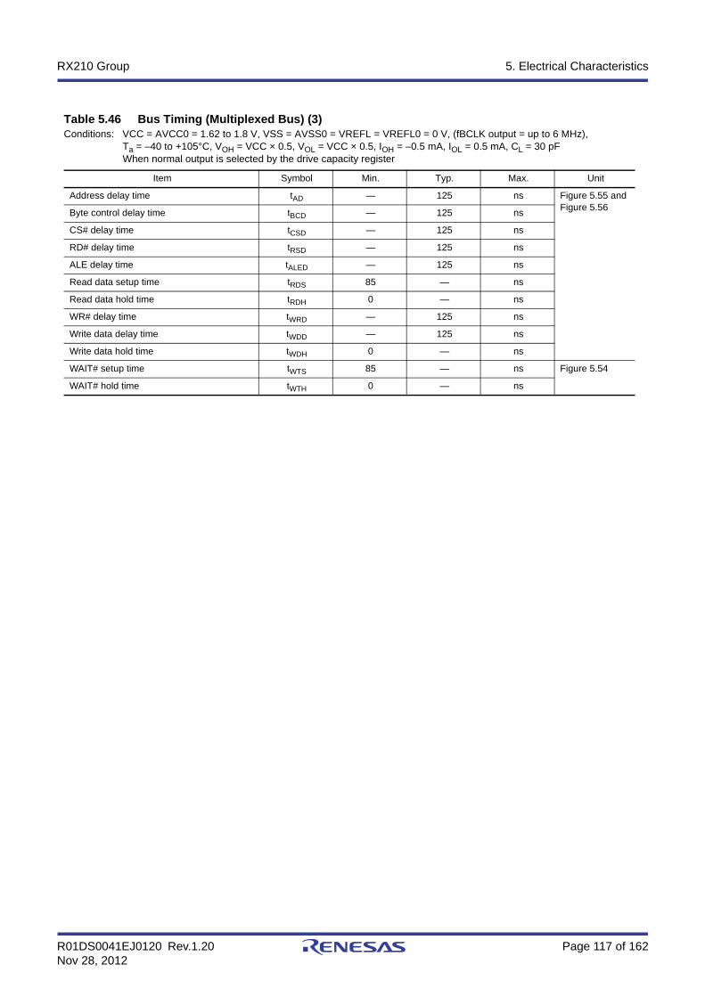
R01DS0041EJ0120 Rev.1.20 Page 117 of 162Nov 28, 2012
RX210 Group 5. Electrical Characteristics
Table 5.46 Bus Timing (Multiplexed Bus) (3)Conditions: VCC = AVCC0 = 1.62 to 1.8 V, VSS = AVSS0 = VREFL = VREFL0 = 0 V, (fBCLK output = up to 6 MHz),
Ta = –40 to +105°C, VOH = VCC × 0.5, VOL = VCC × 0.5, IOH = –0.5 mA, IOL = 0.5 mA, CL = 30 pFWhen normal output is selected by the drive capacity register
Item Symbol Min. Typ. Max. Unit
Address delay time tAD — 125 ns Figure 5.55 and Figure 5.56
Byte control delay time tBCD — 125 ns
CS# delay time tCSD — 125 ns
RD# delay time tRSD — 125 ns
ALE delay time tALED — 125 ns
Read data setup time tRDS 85 — ns
Read data hold time tRDH 0 — ns
WR# delay time tWRD — 125 ns
Write data delay time tWDD — 125 ns
Write data hold time tWDH 0 — ns
WAIT# setup time tWTS 85 — ns Figure 5.54
WAIT# hold time tWTH 0 — ns
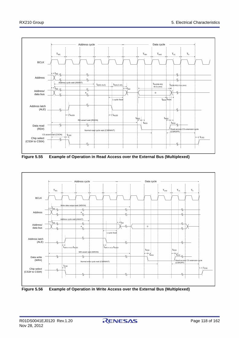
R01DS0041EJ0120 Rev.1.20 Page 118 of 162Nov 28, 2012
RX210 Group 5. Electrical Characteristics
Figure 5.55 Example of Operation in Read Access over the External Bus (Multiplexed)
Figure 5.56 Example of Operation in Write Access over the External Bus (Multiplexed)
Address/data bus
Data read(RD#)
tAD
BCLK
Address
Address latch (ALE)
Chip select(CS3# to CS0#)
TW1 TWn
tAD tAD
tSU(DB-RD)40 ns (min)
Tend
Address cycle Data cycle
tALED
tCSDtCSD
Tn1 Th
1 cycle fixed
Address cycle wait (AWAIT)tS(DB-RD) 0 ns (min)
tRSD
tRSS
tRSD
tRSS
Read-access CS extension cycle (CSROFF)
tALED
RD assert wait (RDON)
Normal read cycle wait (CSRWAIT)
CS assert wait (CSON)
A D
tRDHtRDS
td(AD-ALE) th(ALE-AD)
Address/data bus
Data write(WR#)
tAD
BCLK
Address
Address latch(ALE)
Chip select(CS3# to CS0#)
TW1
tAD tAD
Tend
Address cycle Data cycle
tCSDtCSD
Tn1 Th
1 cycle fixed
td(BCLK-ALE)=tALED
Address cycle wait (AWAIT)
tRSD
tRSS
tRSD
tRSS
WR assert wait (WRON)
Normal write cycle wait (CSRWAIT)
A D
Write data output wait (WDON)
td(BCLK-ALE)=tALED
A
Read-access CS extension cycle (CSROFF)
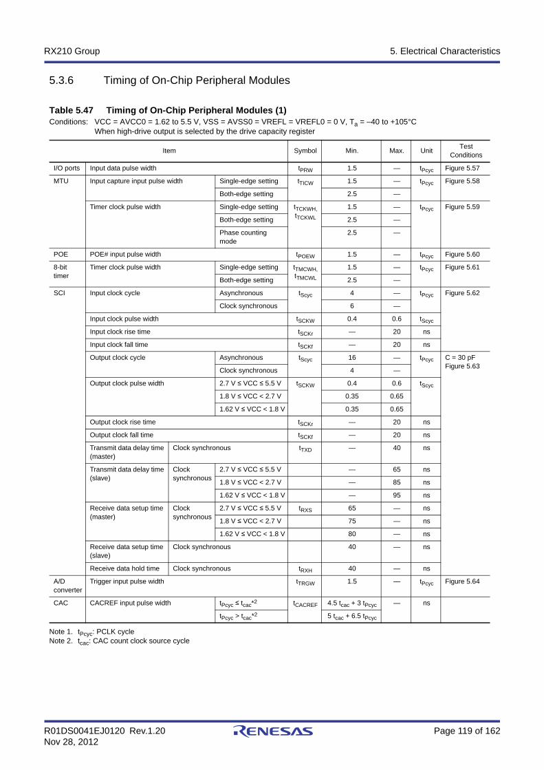
R01DS0041EJ0120 Rev.1.20 Page 119 of 162Nov 28, 2012
RX210 Group 5. Electrical Characteristics
5.3.6 Timing of On-Chip Peripheral Modules
Note 1. tPcyc: PCLK cycleNote 2. tcac: CAC count clock source cycle
Table 5.47 Timing of On-Chip Peripheral Modules (1)Conditions: VCC = AVCC0 = 1.62 to 5.5 V, VSS = AVSS0 = VREFL = VREFL0 = 0 V, Ta = –40 to +105°C
When high-drive output is selected by the drive capacity register
Item Symbol Min. Max. UnitTest
Conditions
I/O ports Input data pulse width tPRW 1.5 — tPcyc Figure 5.57
MTU Input capture input pulse width Single-edge setting tTICW 1.5 — tPcyc Figure 5.58
Both-edge setting 2.5 —
Timer clock pulse width Single-edge setting tTCKWH, tTCKWL
1.5 — tPcyc Figure 5.59
Both-edge setting 2.5 —
Phase counting mode
2.5 —
POE POE# input pulse width tPOEW 1.5 — tPcyc Figure 5.60
8-bit timer
Timer clock pulse width Single-edge setting tTMCWH, tTMCWL
1.5 — tPcyc Figure 5.61
Both-edge setting 2.5 —
SCI Input clock cycle Asynchronous tScyc 4 — tPcyc Figure 5.62
Clock synchronous 6 —
Input clock pulse width tSCKW 0.4 0.6 tScyc
Input clock rise time tSCKr — 20 ns
Input clock fall time tSCKf — 20 ns
Output clock cycle Asynchronous tScyc 16 — tPcyc C = 30 pFFigure 5.63
Clock synchronous 4 —
Output clock pulse width 2.7 V ≤ VCC ≤ 5.5 V tSCKW 0.4 0.6 tScyc
1.8 V ≤ VCC < 2.7 V 0.35 0.65
1.62 V ≤ VCC < 1.8 V 0.35 0.65
Output clock rise time tSCKr — 20 ns
Output clock fall time tSCKf — 20 ns
Transmit data delay time (master)
Clock synchronous tTXD — 40 ns
Transmit data delay time (slave)
Clock synchronous
2.7 V ≤ VCC ≤ 5.5 V — 65 ns
1.8 V ≤ VCC < 2.7 V — 85 ns
1.62 V ≤ VCC < 1.8 V — 95 ns
Receive data setup time (master)
Clock synchronous
2.7 V ≤ VCC ≤ 5.5 V tRXS 65 — ns
1.8 V ≤ VCC < 2.7 V 75 — ns
1.62 V ≤ VCC < 1.8 V 80 — ns
Receive data setup time (slave)
Clock synchronous 40 — ns
Receive data hold time Clock synchronous tRXH 40 — ns
A/Dconverter
Trigger input pulse width tTRGW 1.5 — tPcyc Figure 5.64
CAC CACREF input pulse width tPcyc ≤ tcac*2 tCACREF 4.5 tcac + 3 tPcyc — ns
tPcyc > tcac*2 5 tcac + 6.5 tPcyc
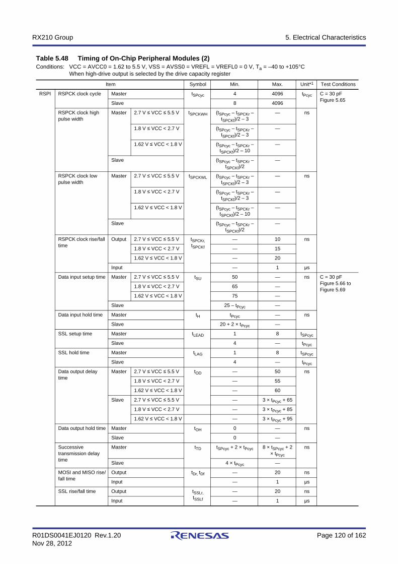
R01DS0041EJ0120 Rev.1.20 Page 120 of 162Nov 28, 2012
RX210 Group 5. Electrical Characteristics
Table 5.48 Timing of On-Chip Peripheral Modules (2)Conditions: VCC = AVCC0 = 1.62 to 5.5 V, VSS = AVSS0 = VREFL = VREFL0 = 0 V, Ta = –40 to +105°C
When high-drive output is selected by the drive capacity register
Item Symbol Min. Max. Unit*1 Test Conditions
RSPI RSPCK clock cycle Master tSPcyc 4 4096 tPcyc C = 30 pFFigure 5.65
Slave 8 4096
RSPCK clock high pulse width
Master 2.7 V ≤ VCC ≤ 5.5 V tSPCKWH (tSPcyc – tSPCKr – tSPCKf)/2 – 3
— ns
1.8 V ≤ VCC < 2.7 V (tSPcyc – tSPCKr – tSPCKf)/2 – 3
—
1.62 V ≤ VCC < 1.8 V (tSPcyc – tSPCKr – tSPCKf)/2 – 10
—
Slave (tSPcyc – tSPCKr – tSPCKf)/2
—
RSPCK clock low pulse width
Master 2.7 V ≤ VCC ≤ 5.5 V tSPCKWL (tSPcyc – tSPCKr – tSPCKf)/2 – 3
— ns
1.8 V ≤ VCC < 2.7 V (tSPcyc – tSPCKr – tSPCKf)/2 – 3
—
1.62 V ≤ VCC < 1.8 V (tSPcyc – tSPCKr – tSPCKf)/2 – 10
—
Slave (tSPcyc – tSPCKr – tSPCKf)/2
—
RSPCK clock rise/fall time
Output 2.7 V ≤ VCC ≤ 5.5 V tSPCKr, tSPCKf
— 10 ns
1.8 V ≤ VCC < 2.7 V — 15
1.62 V ≤ VCC < 1.8 V — 20
Input — 1 μs
Data input setup time Master 2.7 V ≤ VCC ≤ 5.5 V tSU 50 — ns C = 30 pFFigure 5.66 to Figure 5.69
1.8 V ≤ VCC < 2.7 V 65 —
1.62 V ≤ VCC < 1.8 V 75 —
Slave 25 – tPcyc —
Data input hold time Master tH tPcyc — ns
Slave 20 + 2 × tPcyc —
SSL setup time Master tLEAD 1 8 tSPcyc
Slave 4 — tPcyc
SSL hold time Master tLAG 1 8 tSPcyc
Slave 4 — tPcyc
Data output delay time
Master 2.7 V ≤ VCC ≤ 5.5 V tOD — 50 ns
1.8 V ≤ VCC < 2.7 V — 55
1.62 V ≤ VCC < 1.8 V — 60
Slave 2.7 V ≤ VCC ≤ 5.5 V — 3 × tPcyc + 65
1.8 V ≤ VCC < 2.7 V — 3 × tPcyc + 85
1.62 V ≤ VCC < 1.8 V — 3 × tPcyc + 95
Data output hold time Master tOH 0 — ns
Slave 0 —
Successive transmission delay time
Master tTD tSPcyc + 2 × tPcyc 8 × tSPcyc + 2 × tPcyc
ns
Slave 4 × tPcyc —
MOSI and MISO rise/fall time
Output tDr, tDf — 20 ns
Input — 1 μs
SSL rise/fall time Output tSSLr, tSSLf
— 20 ns
Input — 1 μs

R01DS0041EJ0120 Rev.1.20 Page 121 of 162Nov 28, 2012
RX210 Group 5. Electrical Characteristics
Note 1. tPcyc: PCLK cycle
Note 1. tPcyc: PCLK cycle
RSPI Slave access time 2.7 V ≤ VCC ≤ 5.5 V tSA — 6 tPcyc C = 30 pFFigure 5.68 and Figure 5.69
1.8 V ≤ VCC < 2.7 V — 7
1.62 V ≤ VCC < 1.8 V — 7
Slave output release time 2.7 V ≤ VCC ≤ 5.5 V tREL — 5 tPcyc
1.8 V ≤ VCC < 2.7 V — 6
1.62 V ≤ VCC < 1.8 V — 6
Table 5.49 Timing of On-Chip Peripheral Modules (3)Conditions: VCC = AVCC0 = 1.62 to 5.5 V, VSS = AVSS0 = VREFL = VREFL0 = 0 V, Ta = –40 to +105°C
When high-drive output is selected by the drive capacity register
Item Symbol Min. Max. Unit*1 Test Conditions
Simple SPI
SCK clock cycle output (master) tSPcyc 4 65536 tPcyc C = 30 pFFigure 5.65
SCK clock cycle input (slave) 6 65536
SCK clock high pulse width tSPCKWH 0.4 0.6 tSPcyc
SCK clock low pulse width tSPCKWL 0.4 0.6 tSPcyc
SCK output clock high pulse width
2.7 V ≤ VCC ≤ 5.5 V tSPCKWH 0.4 0.6 tSPcyc
1.8 V ≤ VCC < 2.7 V 0.35 0.65
1.62 V ≤ VCC < 1.8 V 0.35 0.65
SCK output clock low pulse width
2.7 V ≤ VCC ≤ 5.5 V tSPCKWL 0.4 0.6 tSPcyc
1.8 V ≤ VCC < 2.7 V 0.35 0.65
1.62 V ≤ VCC < 1.8 V 0.35 0.65
SCK clock rise/fall time tSPCKr, tSPCKf — 20 ns
Data input setup time (Master)
2.7 V ≤ VCC ≤ 5.5 V tSU 65 — ns C = 30 pFFigure 5.66 and Figure 5.69
1.8 V ≤ VCC < 2.7 V 75 —
1.62 V ≤ VCC < 1.8 V 80 —
Data input setup time (Slave) 40 —
Data input hold time tH 40 — ns
SS input setup time tLEAD 1 — tSPcyc
SS input hold time tLAG 1 — tSPcyc
Data output delay time (Master) tOD — 40 ns
Data output delay time (Slave)
2.7 V ≤ VCC ≤ 5.5 V — 65
1.8 V ≤ VCC < 2.7 V — 85
1.62 V ≤ VCC < 1.8 V — 95
Data output hold time tOH –10 — ns
Data rise/fall time tDr, tDf — 20 ns
SS input rise/fall time tSSLr, tSSLf — 20 ns
Slave access time tSA — 6 tPcyc C = 30 pFFigure 5.68 and Figure 5.69
Slave output release time tREL — 6 tPcyc
Item Symbol Min. Max. Unit*1 Test Conditions

R01DS0041EJ0120 Rev.1.20 Page 122 of 162Nov 28, 2012
RX210 Group 5. Electrical Characteristics
Note: • tIICcyc: RIIC internal reference count clock (IICφ) cycleNote 1. The value in parentheses is used when the ICMR3.NF[1:0] bits are set to 11b while a digital filter is enabled with the
ICFER.NFEbits = 1.Note 2. Cb indicates the total capacity of the bus line.
Table 5.50 Timing of On-Chip Peripheral Modules (4)Conditions: VCC = AVCC0 = 2.7 to 5.5 V, VSS = AVSS0 = VREFL = VREFL0 = 0 V, fPCLKB = up to 32 MHz,
Ta = –40 to +105°C
Item Symbol Min.*1,*2 Max. UnitTest
Conditions
RIIC(Standard mode, SMBus)
SCL input cycle time tSCL 6 (12) × tIICcyc + 1300 — ns Figure 5.70
SCL input high pulse width tSCLH 3 (6) × tIICcyc + 300 — ns
SCL input low pulse width tSCLL 3 (6) × tIICcyc + 300 — ns
SCL, SDA input rise time tSr — 1000 ns
SCL, SDA input fall time tSf — 300 ns
SCL, SDA input spike pulse removal time tSP 0 1 (4) × tIICcyc ns
SDA input bus free time tBUF 3 (6) × tIICcyc + 300 — ns
Start condition input hold time tSTAH tIICcyc + 300 — ns
Restart condition input setup time tSTAS 1000 — ns
Stop condition input setup time tSTOS 1000 — ns
Data input setup time tSDAS tIICcyc + 50 — ns
Data input hold time tSDAH 0 — ns
SCL, SDA capacitive load Cb — 400 pF
RIIC(Fast mode)
SCL input cycle time tSCL 6 (12) × tIICcyc + 600 — ns Figure 5.70
SCL input high pulse width tSCLH 3 (6) × tIICcyc + 300 — ns
SCL input low pulse width tSCLL 3 (6) × tIICcyc + 300 — ns
SCL, SDA input rise time tSr 20 + 0.1Cb 300 ns
SCL, SDA input fall time tSf 20 + 0.1Cb 300 ns
SCL, SDA input spike pulse removal time tSP 0 1 (4) × tIICcyc ns
SDA input bus free time tBUF 3 (6) × tIICcyc + 300 — ns
Start condition input hold time tSTAH tIICcyc + 300 — ns
Restart condition input setup time tSTAS 300 — ns
Stop condition input setup time tSTOS 300 — ns
Data input setup time tSDAS tIICcyc + 50 — ns
Data input hold time tSDAH 0 — ns
SCL, SDA capacitive load Cb — 400 pF

R01DS0041EJ0120 Rev.1.20 Page 123 of 162Nov 28, 2012
RX210 Group 5. Electrical Characteristics
Note: • tPcyc: PCLK cycleNote 1. Cb indicates the total capacity of the bus line.Note 2. This applies when the SMR.CKS[1:0] bits = 00b and the SNFR.NFCS[2:0] bits = 010b while the SNFR.NFE bit = 1 and the digital
filter is enabled.
Table 5.51 Timing of On-Chip Peripheral Modules (5)Conditions: VCC = AVCC0 = 2.7 to 5.5 V, VSS = AVSS0 = VREFL = VREFL0 = 0 V, fPCLKB = up to 32 MHz,
Ta = –40 to +105°CWhen high-drive output is selected by the drive capacity register
Item Symbol Min.*1 Max. UnitTest
Conditions
Simple IIC(Standard mode)
SDA input rise time tSr — 1000 ns Figure 5.70
SDA input fall time tSf — 300 ns
SDA input spike pulse removal time tSP 0 4 × tpcyc*2 ns
Data input setup time tSDAS 250 — ns
Data input hold time tSDAH 0 — ns
SCL, SDA capacitive load Cb — 400 pF
Simple IIC(Fast mode)
SCL, SDA input rise time tSr 20 + 0.1Cb 300 ns Figure 5.70
SCL, SDA input fall time tSf 20 + 0.1Cb 300 ns
SCL, SDA input spike pulse removal time tSP 0 4 × tpcyc*2 ns
Data input setup time tSDAS 100 — ns
Data input hold time tSDAH 0 — ns
SCL, SDA capacitive load Cb — 400 pF
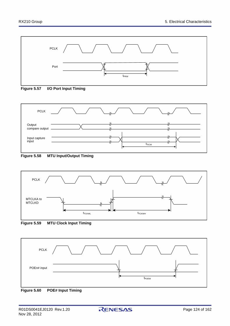
R01DS0041EJ0120 Rev.1.20 Page 124 of 162Nov 28, 2012
RX210 Group 5. Electrical Characteristics
Figure 5.57 I/O Port Input Timing
Figure 5.58 MTU Input/Output Timing
Figure 5.59 MTU Clock Input Timing
Figure 5.60 POE# Input Timing
Port
PCLK
tPRW
Output compare output
Input capture input
PCLK
tTICW
MTCLKA to MTCLKD
PCLK
tTCKWL tTCKWH
POEn# input
PCLK
tPOEW

R01DS0041EJ0120 Rev.1.20 Page 125 of 162Nov 28, 2012
RX210 Group 5. Electrical Characteristics
Figure 5.61 8-Bit Timer Clock Input Timing
Figure 5.62 SCK Clock Input Timing
Figure 5.63 SCI Input/Output Timing: Clock Synchronous Mode
Figure 5.64 A/D Converter External Trigger Input Timing
PCLK
TMCI0 to TMCI3
tTMCWL tTMCWH
tSCKW tSCKr tSCKf
tScyc
SCKn(n = 0, 1, 5, 6, 8, 9, 12)
tTXD
tRXS tRXH
TXDn
RXDn
SCKn
n = 0, 1, 5, 6, 8, 9, 12
ADTRG0#
PCLK
tTRGW
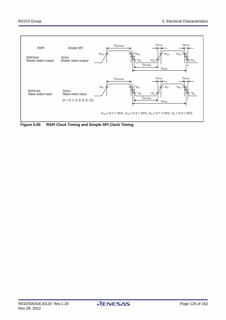
R01DS0041EJ0120 Rev.1.20 Page 126 of 162Nov 28, 2012
RX210 Group 5. Electrical Characteristics
Figure 5.65 RSPI Clock Timing and Simple SPI Clock Timing
SCKnMaster select output
SCKnSlave select input
(n = 0, 1, 5, 6, 8, 9, 12)
tSPCKWH
VOH VOH
VOL VOL
VOH VOH
tSPCKWL
tSPCKr tSPCKf
VOL
tSPcyc
tSPCKWH
VIH VIH
VIL VIL
VIH VIH
tSPCKWL
tSPCKr tSPCKf
VIL
tSPcyc
VOH = 0.7 × VCC, VOL = 0.3 × VCC, VIH = 0.7 × VCC, VIL = 0.3 × VCC
RSPCKAMaster select output
RSPCKASlave select input
Simple SPIRSPI
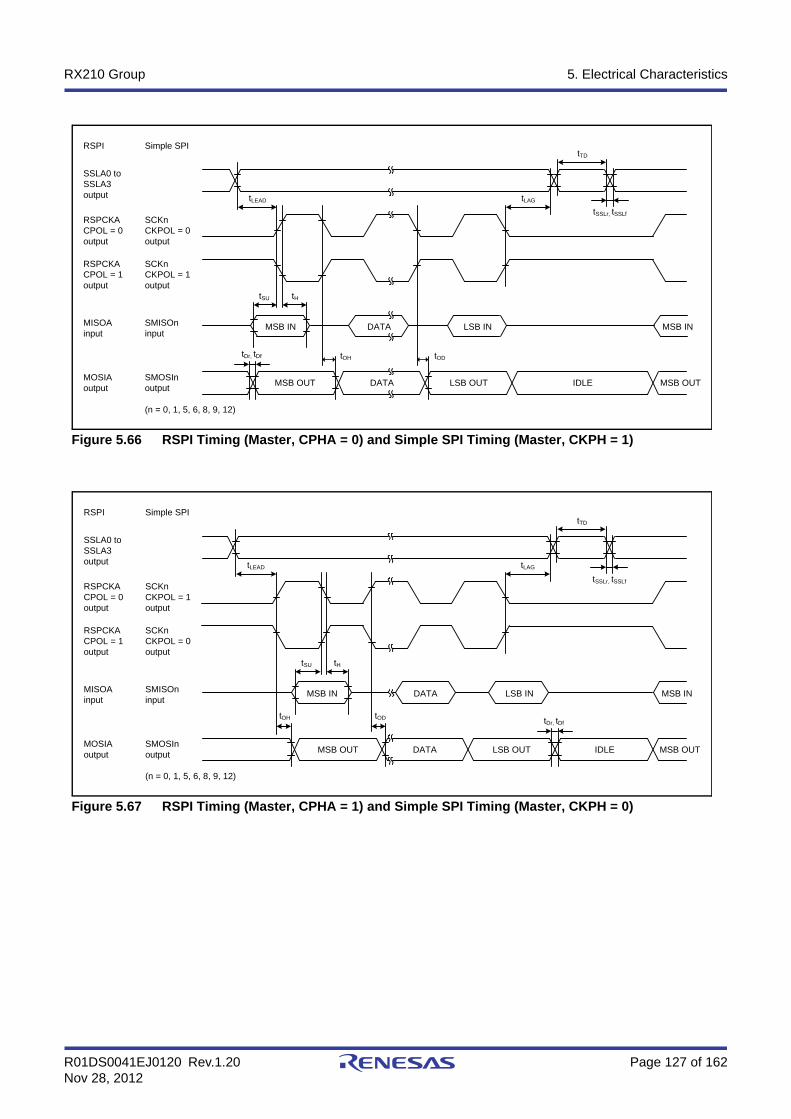
R01DS0041EJ0120 Rev.1.20 Page 127 of 162Nov 28, 2012
RX210 Group 5. Electrical Characteristics
Figure 5.66 RSPI Timing (Master, CPHA = 0) and Simple SPI Timing (Master, CKPH = 1)
Figure 5.67 RSPI Timing (Master, CPHA = 1) and Simple SPI Timing (Master, CKPH = 0)
tDr, tDf
tSU tH
tLEAD
tTD
tLAG
tSSLr, tSSLf
tOH tOD
MSB IN DATA LSB IN MSB IN
MSB OUT DATA LSB OUT IDLE MSB OUT
SCKnCKPOL = 0output
SCKnCKPOL = 1output
SMISOninput
SMOSInoutput
(n = 0, 1, 5, 6, 8, 9, 12)
Simple SPIRSPI
SSLA0 to SSLA3output
RSPCKACPOL = 0output
RSPCKACPOL = 1output
MISOAinput
MOSIAoutput
tDr, tDf
tSU tH
tLEAD
tTD
tLAG
tSSLr, tSSLf
tOH
MSB IN DATA LSB IN MSB IN
MSB OUT DATA LSB OUT IDLE MSB OUT
tOD
SCKnCKPOL = 1output
SCKnCKPOL = 0output
SMISOninput
SMOSInoutput
(n = 0, 1, 5, 6, 8, 9, 12)
Simple SPIRSPI
SSLA0 to SSLA3output
RSPCKACPOL = 0output
RSPCKACPOL = 1output
MISOAinput
MOSIAoutput

R01DS0041EJ0120 Rev.1.20 Page 128 of 162Nov 28, 2012
RX210 Group 5. Electrical Characteristics
Figure 5.68 RSPI Timing (Slave, CPHA = 0) and Simple SPI Timing (Slave, CKPH = 1)
Figure 5.69 RSPI Timing (Slave, CPHA = 1) and Simple SPI Timing (Slave, CKPH = 0)
tDr, tDftSU tH
tLEAD
tTD
tLAG
tSA
MSB IN DATA LSB IN MSB IN
MSB OUT DATA LSB OUT MSB IN MSB OUT
tOH tOD tREL
SCKnCKPOL = 0input
SCKnCKPOL = 1input
SMISOnoutput
SMOSIninput
(n = 0, 1, 5, 6, 8, 9, 12)
Simple SPIRSPI
SSLA0input
RSPCKACPOL = 0input
RSPCKACPOL = 1input
MISOAoutput
MOSIAinput
SSn#input
tDr, tDf
tSA tOH
tLEAD
tTD
tLAG
tH
LSB OUT(Last data) DATA MSB OUT
MSB IN DATA LSB IN MSB IN
LSB OUT
tSU
tOD tREL
MSB OUT
SCKnCKPOL = 1input
SCKnCKPOL = 0input
SMISOnoutput
SMOSIninput
(n = 0, 1, 5, 6, 8, 9, 12)
Simple SPIRSPI
SSLA0input
RSPCKACPOL = 0input
RSPCKACPOL = 1input
MISOAoutput
MOSIAinput
SSn#input
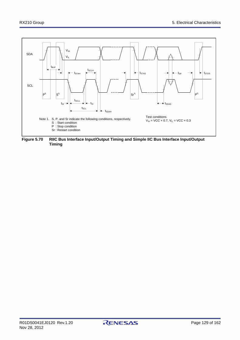
R01DS0041EJ0120 Rev.1.20 Page 129 of 162Nov 28, 2012
RX210 Group 5. Electrical Characteristics
Figure 5.70 RIIC Bus Interface Input/Output Timing and Simple IIC Bus Interface Input/Output Timing
Test conditionsVIH = VCC × 0.7, VIL = VCC × 0.3
SDA
SCL
VIH
VIL
tSTAH
tSCLH
tSCLL
P*1 S*1
tSf tSr
tSCLtSDAH
tSDAS
tSTAS tSP tSTOS
P*1
tBUF
Sr*1
Note 1. S, P, and Sr indicate the following conditions, respectively.S : Start conditionP : Stop conditionSr : Restart condition

R01DS0041EJ0120 Rev.1.20 Page 130 of 162Nov 28, 2012
RX210 Group 5. Electrical Characteristics
5.4 A/D Conversion Characteristics
Note: • PCLKD must be set to 40 MHz or lower when HOCO is to be selected as the A/D conversion clock. The characteristics apply when no pin functions other than A/D converter input are used. Absolute accuracy includes quantization errors. Offset error, full-scale error, DNL differential nonlinearity error, and INL integral nonlinearity error do not include quantization errors.
Note 1. The conversion time is the sum of the sampling time and the comparison time. As the test conditions, the number of sampling states is indicated.
Note 2. The value in parentheses indicates the sampling time.Note 3. The lower-limit frequency of PCLKD is 1 MHz.Note 4. When using the temperature sensor, use it when AVCC0 = VREFH0.
Table 5.52 A/D Conversion Characteristics (1)Conditions: VCC = AVCC0 = 2.7 to 5.5 V, 2.7 V VREFH0 = (AVCC0 - 0.9 V) to AVCC0*4,
VSS = AVSS0 = VREFL = VREFL0 = 0 V, fPCLKD = 1 to 50 MHz, Ta = –40 to +105°C
Item Min. Typ. Max. Unit Test Conditions
Resolution — — 12 Bit
Conversion time*1
(Operation at fPCLKD = 50 MHz)*3
Permissible signal source impedance (Max.) = 0.5 kΩ
1.0 (0.4)*2
— — µs Sampling in 20 states
Permissible signal source impedance (Max.) = 1 kΩ
1.1 (0.5)*2
— — Sampling in 25 states
Permissible signal source impedance (Max.) = 5 kΩ
1.5 (0.9)*2
— — Sampling in 45 states
Analog input capacitance — — 30 pF
Offset error — ±0.5 ±4.5 LSB High-precision channel
±7.5 Normal-precision channel
Full-scale error — ±0.75 ±4.5 LSB High-precision channel
±7.5 Normal-precision channel
Quantization error — ±0.5 — LSB
Absolute accuracy — ±1.25 ±5.0 LSB High-precision channel
— ±1.25 ±8.0 LSB Normal-precision channel
DNL differential nonlinearity error — ±1.0 — LSB
INL integral nonlinearity error — ±1.0 ±3.0 LSB
Table 5.53 Channel Classification for A/D Converter
Classification Channel Conditions
High-precision channel AN003 to AN007 AVCC0 = 1.62 to 5.5 V It is disallowed to use pins AN000 to AN007 as digital outputs when the A/D con-verter is used.
AN000, AN001, AN002 AVCC0 = 2.7 to 5.5 V, when the sample and hold circuit is in use.
AVCC0 = 1.62 to 5.5 V, when the sample and hold circuit is not in use.
Normal-precision channel AN008 to AN015 AVCC0 = 1.62 to 5.5 V
Table 5.54 A/D Internal Reference Voltage CharacteristicsConditions: VCC = AVCC0 = 1.62 to 5.5 V, VSS = AVSS0 = VREFL = VREFL0 = 0 V, Ta = 40 to +105
Item Min. Typ. Max. Unit Test Conditions
A/D internal reference voltage 1.35 1.50 1.65 V

R01DS0041EJ0120 Rev.1.20 Page 131 of 162Nov 28, 2012
RX210 Group 5. Electrical Characteristics
Note: • The characteristics apply when no pin functions other than A/D converter input are used. Absolute accuracy includes quantization errors. Offset error, full-scale error, DNL differential nonlinearity error, and INL integral nonlinearity error do not include quantization errors.
Note 1. The conversion time is the sum of the sampling time and the comparison time. As the test conditions, the number of sampling states is indicated.
Note 2. The value in parentheses indicates the sampling time.Note 3. The lower-limit frequency of PCLKD is 1 MHz.Note 4. When using the temperature sensor, use it when AVCC0 = VREFH0.
Note: • The characteristics apply when no pin functions other than A/D converter input are used. Absolute accuracy includes quantization errors. Offset error, full-scale error, DNL differential nonlinearity error, and INL integral nonlinearity error do not include quantization errors.
Note 1. The conversion time is the sum of the sampling time and the comparison time. As the test conditions, the number of sampling states is indicated.
Note 2. The value in parentheses indicates the sampling time.Note 3. The lower-limit frequency of PCLKD is 1 MHz.
Table 5.55 A/D Conversion Characteristics (2)Conditions: VCC = AVCC0 = 1.8 to 3.6 V, VREFH0 = (AVCC0 – 0.9 V) to AVCC0, VREFH0 = 1.8 to 2.7 V*4,
VSS = AVSS0 = VREFL = VREFL0 = 0 V, fPCLKD = 1 to 32 MHz, Ta = –40 to +105°C
Item Min. Typ. Max. Unit Test Conditions
Resolution — — 12 Bit
Conversion time*1
(Operation at fPCLKD = 25 MHz)*3
Permissible signal source impedance (Max.) = 1 kΩ
2.0 (0.8)*2
— — µs Sampling in 20 states
Permissible signal source impedance (Max.) = 5 kΩ
2.2 (1.0)*2
— — Sampling in 25 states
Analog input capacitance — — 30 pF
Offset error — ±0.5 ±7.5 LSB
Full-scale error — ±1.25 ±7.5 LSB
Quantization error — ±0.5 — LSB
Absolute accuracy — ±3.0 ±8.0 LSB
DNL differential nonlinearity error — ±1.25 — LSB
INL integral nonlinearity error — ±1.5 ±3.0 LSB
Table 5.56 A/D Conversion Characteristics (3)Conditions: VCC = AVCC0 = 1.62 to 1.8 V, VREFH0 = AVCC0,
VSS = AVSS0 = VREFL = VREFL0 = 0 V, fPCLKD = 1 to 16 MHz, Ta = –40 to +105°C
Item Min. Typ. Max. Unit Test Conditions
Resolution — — 12 Bit
Conversion time*1
(Operation at fPCLKD = 12.5 MHz)*3
Permissible signal source impedance (Max.) = 1 kΩ
3.36 (0.96)*2
— — µs Sampling in 12 states
Permissible signal source impedance (Max.) = 5 kΩ
3.6 (1.2)*2
— — Sampling in 15 states
Analog input capacitance — — 30 pF
Offset error — ±0.5 ±7.5 LSB
Full-scale error — ±1.25 ±7.5 LSB
Quantization error — ±0.5 — LSB
Absolute accuracy — ±2.75 ±8.0 LSB
DNL differential nonlinearity error — ±1.25 — LSB
INL integral nonlinearity error — ±1.25 ±3.0 LSB

R01DS0041EJ0120 Rev.1.20 Page 132 of 162Nov 28, 2012
RX210 Group 5. Electrical Characteristics
Figure 5.71 Internal Equivalent Circuit of Analog Input Pin
Table 5.57 Sampling TimeConditions: VCC = AVCC0 = 1.62 to 5.5 V, VSS = AVSS0 = VREFL = VREFL0 = 0 V, Ta = –40 to +105°C
Item Symbol Typ. Unit Test Conditions
Sampling time High-precision channel Ts 0.2 + 0.14 × R0 (KΩ) µs Figure 5.71
Normal-precision channel 0.35 + 0.14 × R0 (KΩ)
R0
ANi
RX210

R01DS0041EJ0120 Rev.1.20 Page 133 of 162Nov 28, 2012
RX210 Group 5. Electrical Characteristics
Figure 5.72 Illustration of A/D Converter Characteristic Terms
Absolute accuracy
Absolute accuracy is the difference between output code based on the theoretical A/D conversion characteristics, and the
actual A/D conversion result. When measuring absolute accuracy, the voltage at the midpoint of the width of analog
input voltage (1-LSB width), that can meet the expectation of outputting an equal code based on the theoretical A/D
conversion characteristics, is used as an analog input voltage. For example, if 12-bit resolution is used and if reference
voltage (AVREFH0) = 5.12 V, then 1-LSB width becomes 1.25 mV, and 0 mV, 1.25 mV, 2.5 mV, ... are used as analog
input voltages.
If analog input voltage is 10 mV, absolute accuracy = ±5 LSB means that the actual A/D conversion result is in the range
of 003h to 00Dh though an output code, 008h, can be expected from the theoretical A/D conversion characteristics.
Integral nonlinearity error (INL)
Integral nonlinearity error is the maximum deviation between the ideal line when the measured offset and full-scale
errors are zeroed, and the actual output code.
Integral nonlinearity error (INL)
Actual A/D conversion characteristic
Ideal A/D conversion characteristic
Analog input voltage
Offset error
Absolute accuracy
Differential nonlinearity error (DNL)
Full-scale errorFFFh
000h
0
Ideal line of actual A/D conversion characteristic
1-LSB width for ideal A/D conversion characteristic
Differential nonlinearity error (DNL)
1-LSB width for ideal A/D conversion characteristic
AVREFH0(full-scale)
A/D converteroutput code
R01DS0041EJ0120 Rev.1.20 Page 134 of 162Nov 28, 2012
RX210 Group 5. Electrical Characteristics
Differential nonlinearity error (DNL)
Differential nonlinearity error is the difference between 1-LSB width based on the ideal AD conversion characteristics
and the width of the actually output code.
Offset error
Offset error is the difference between a transition point of the ideal first output code and the actual first output code.
Full-scale error
Full-scale error is the difference between a transition point of the ideal last output code and the actual last output code.
R01DS0041EJ0120 Rev.1.20 Page 135 of 162Nov 28, 2012
RX210 Group 5. Electrical Characteristics
5.5 D/A Conversion Characteristics
5.6 Temperature Sensor Characteristics
Table 5.58 D/A Conversion Characteristics (1)Conditions: VCC = AVCC0 = 2.7 to 5.5 V, VREFH = 2.7 V to AVCC0,
VSS = AVSS0 = VREFL = VREFL0 = 0 V, fPCLKB = up to 32 MHz, Ta = –40 to +105°C
Item Min. Typ. Max. Unit Test Conditions
Resolution — — 10 Bit
Conversion time — — 3.0 µs 20-pF capacitive load
Absolute accuracy — ±3.0 ±5.0 LSB 4-MΩ resistive load
— — ±4.0 LSB 8-MΩ resistive load
RO output resistance — 4.1 — kΩ
Table 5.59 D/A Conversion Characteristics (2)Conditions: VCC = AVCC0 = 2.7 to 5.5 V, VREFH =1.8 V to AVCC0,
VSS = AVSS0 = VREFL = VREFL0 = 0 V, fPCLKB = up to 32 MHz, Ta = –40 to +105°C
Item Min. Typ. Max. Unit Test Conditions
Resolution — — 10 Bit
Conversion time — — 10.0 µs 20-pF capacitive load
Absolute accuracy — ±5.0 ±6.0 LSB 4-MΩ resistive load
— — ±5.0 LSB 8-MΩ resistive load
RO output resistance — 4.1 — kΩ
Table 5.60 Temperature Sensor CharacteristicsConditions: VCC = AVCC0 = VREFH0 = 1.8 to 5.5 V, VSS = AVSS0 = VREFL = VREFL0 = 0 V, Ta = –40 to +105°C
Item Symbol Min. Typ. Max. Unit Test Conditions
Relative accuracy ― ― ±1.0 ― °C
Temperature slope 1.8 ≤ AVCC0 < 2.7 ― ― 7.27 ― mV/°C PGAGAIN = 00b
2.7 ≤ AVCC0 < 3.6 ― 10.46 ― PGAGAIN = 01b
3.6 ≤ AVCC0 < 4.5 ― 13.98 ― PGAGAIN = 10b
4.5 ≤ AVCC0 ≤ 5.5 ― 21.65 ― PGAGAIN = 11b
Output voltage (@25°C) ― ― 1.375 ― V VCC = 3.6 V
Temperature sensor start time tSTART ― ― 80 µs Figure 5.73
Sampling time ― 30 72 300 µs
PGA restart time tRST_PGA ― ― 40 µs
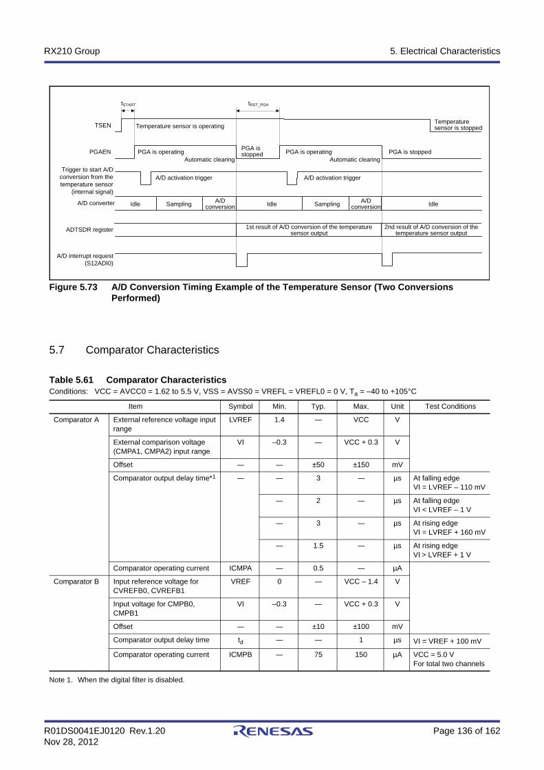
R01DS0041EJ0120 Rev.1.20 Page 136 of 162Nov 28, 2012
RX210 Group 5. Electrical Characteristics
Figure 5.73 A/D Conversion Timing Example of the Temperature Sensor (Two Conversions Performed)
5.7 Comparator Characteristics
Note 1. When the digital filter is disabled.
Table 5.61 Comparator CharacteristicsConditions: VCC = AVCC0 = 1.62 to 5.5 V, VSS = AVSS0 = VREFL = VREFL0 = 0 V, Ta = –40 to +105°C
Item Symbol Min. Typ. Max. Unit Test Conditions
Comparator A External reference voltage input range
LVREF 1.4 ― VCC V
External comparison voltage (CMPA1, CMPA2) input range
VI –0.3 ― VCC + 0.3 V
Offset ― ― ±50 ±150 mV
Comparator output delay time*1 ― ― 3 ― µs At falling edgeVI = LVREF – 110 mV
― 2 ― µs At falling edgeVI < LVREF – 1 V
― 3 ― µs At rising edgeVI = LVREF + 160 mV
― 1.5 ― µs At rising edgeVI > LVREF + 1 V
Comparator operating current ICMPA ― 0.5 ― µA
Comparator B Input reference voltage for CVREFB0, CVREFB1
VREF 0 ― VCC – 1.4 V
Input voltage for CMPB0, CMPB1
VI –0.3 ― VCC + 0.3 V
Offset ― ― ±10 ±100 mV
Comparator output delay time td ― ― 1 µs VI = VREF + 100 mV
Comparator operating current ICMPB ― 75 150 µA VCC = 5.0 VFor total two channels
A/D interrupt request(S12ADI0)
TSEN
PGAEN
tSTART tRST_PGA
Trigger to start A/D conversion from the temperature sensor
(internal signal)
A/D converter
A/D activation trigger
PGA is stopped
IdleA/D conversionSamplingIdleA/D
conversionSamplingIdle
1st result of A/D conversion of the temperature sensor output
2nd result of A/D conversion of the temperature sensor output
Temperature sensor is stoppedTemperature sensor is operating
PGA is operating PGA is operatingPGA is stopped
Automatic clearing Automatic clearing
A/D activation trigger
ADTSDR register

R01DS0041EJ0120 Rev.1.20 Page 137 of 162Nov 28, 2012
RX210 Group 5. Electrical Characteristics
5.8 Power-on Reset Circuit and Voltage Detection Circuit Characteristics
Note: • These characteristics apply when noise is not superimposed on the power supply.Note 1. When the CPU is in a mode other than software standby and deep software standby modes, when the CPU transits to software
standby mode with the FHSSBYCR.SOFTCUT[2] bit set to 0, or when the CPU transits to deep software standby mode with the DPSBYCR.DEEPCUT1 bit set to 0.
Note 2. When the CPU transits to software standby mode with the FHSSBYCR.SOFTCUT[2] bit set to 1 or when the CPU transits to deep software standby mode with the DPSBYCR.DEEPCUT1 bit set to 1.
Note 3. # in the symbol Vdet0_# denotes the value of the LDSEL[1:0] bits.Note 4. # in the symbol Vdet1_# denotes the value of the LVDLVLR.LVD1LVL[3:0] bits.
Table 5.62 Power-on Reset Circuit and Voltage Detection Circuit Characteristics (1)Conditions: VCC = AVCC, VSS = AVSS0 = VREFL = VREFL0 = 0 V, Ta = –40 to +105°C
Item Symbol Min. Typ. Max. Unit Test Conditions
Voltage detection level
Power-on reset (POR)
Low power consumption function disabled*1
VPOR 1.30 1.40 1.55 V Figure 5.74 and Figure 5.75
Low power consumption function enabled*2
1.00 1.20 1.45
Voltage detection circuit (LVD0)*3 Vdet0_0 3.65 3.80 3.95 V Figure 5.76
Vdet0_1 2.70 2.80 2.90
Vdet0_2 1.80 1.90 2.00
Vdet0_3 1.62 1.72 1.82
Voltage detection circuit (LVD1)*4 Vdet1_0 4.00 4.15 4.30 V Figure 5.77
At falling edge VCC
Vdet1_1 3.85 4.00 4.15
Vdet1_2 3.70 3.85 4.00
Vdet1_3 3.55 3.70 3.85
Vdet1_4 3.40 3.55 3.70
Vdet1_5 3.25 3.40 3.55
Vdet1_6 3.10 3.25 3.40
Vdet1_7 2.95 3.10 3.25
Vdet1_8 2.85 2.95 3.05
Vdet1_9 2.70 2.80 2.90
Vdet1_A 2.55 2.65 2.75
Vdet1_B 2.40 2.50 2.60
Vdet1_C 2.25 2.35 2.45
Vdet1_D 2.10 2.20 2.30
Vdet1_E 1.95 2.05 2.15
Vdet1_F 1.80 1.90 2.00
R01DS0041EJ0120 Rev.1.20 Page 138 of 162Nov 28, 2012
RX210 Group 5. Electrical Characteristics
Note: • These characteristics apply when noise is not superimposed on the power supply.Note 1. # in the symbol Vdet2_# denotes the value of the LVDLVLR.LVD2LVL[3:0] bits.Note 2. The minimum VCC down time indicates the time when VCC is below the minimum value of voltage detection levels VPOR, Vdet0,
Vdet1, and Vdet2 for the POR/ LVD.
Table 5.63 Power-on Reset Circuit and Voltage Detection Circuit Characteristics (2)Conditions: VCC = AVCC0, VSS = AVSS0 = VREFL = VREFL0 = 0 V, Ta = –40 to +105°C
Item Symbol Min. Typ. Max. Unit Test Conditions
Voltage detection level
Voltage detection circuit (LVD2)*1 Vdet2_0 4.00 4.15 4.30 V Figure 5.78
At falling edge VCC
Vdet2_1 3.85 4.00 4.15
Vdet2_2 3.70 3.85 4.00
Vdet2_3 3.55 3.70 3.85
Vdet2_4 3.40 3.55 3.70
Vdet2_5 3.25 3.40 3.55
Vdet2_6 3.10 3.25 3.40
Vdet2_7 2.95 3.10 3.25
Vdet2_8 2.85 2.95 3.05
Vdet2_9 2.70 2.80 2.90
Vdet2_A 2.55 2.65 2.75
Vdet2_B 2.40 2.50 2.60
Vdet2_C 2.25 2.35 2.45
Vdet2_D 2.10 2.20 2.30
Vdet2_E 1.95 2.05 2.15
Vdet2_F 1.80 1.90 2.00
VCMPA2 1.18 1.33 1.48 EXVCCINP2 = 1
Internal reset time Power-on reset time tPOR — 9 — ms Figure 5.75
Voltage monitoring 0 reset time tLVD0 — 9 — Figure 5.76
Voltage monitoring 1 reset time tLVD1 — 1.4 — Figure 5.77
Voltage monitoring 2 reset time tLVD2 — 1.4 — Figure 5.78
Minimum VCC down time*2 tVOFF 200 — — µs Figure 5.75
Response delay time tdet — — 200 µs Figure 5.75
LVD operation stabilization time (after LVD is enabled) Td(E-A) — — 15 µs Figure 5.77 and Figure 5.78
Power-on reset enable time tW(POR) 1 — — ms Figure 5.75VCC = 0.9 V or lower
Hysteresis width (LVD1 and LVD2) V LVH — 100 — mV When selection is from among VdetX_0 to 7.
— 50 — When selection is from among VdetX_8 to F.

R01DS0041EJ0120 Rev.1.20 Page 139 of 162Nov 28, 2012
RX210 Group 5. Electrical Characteristics
Figure 5.74 Voltage Detection Reset Timing
Figure 5.75 Power-on Reset Timing
Figure 5.76 Voltage Detection Circuit Timing (Vdet0)
tVOFF
tPORtdettdet
VPOR
VCC
Internal reset signal(active-low)
VPOR
0.9 V
tw(por)
tPORtdet
VCC
*1Internal reset signal(active-low)
Note 1. tw(por) is the time required for a power-on reset to be enabled while the external power VCC is being held below the valid voltage (0.9 V).When VCC turns on, maintain tw(por) for 1 ms or more.
VPOR
tVOFF
tLVD0tdet
Vdet0VCC
Internal reset signal(active-low)
tdet

R01DS0041EJ0120 Rev.1.20 Page 140 of 162Nov 28, 2012
RX210 Group 5. Electrical Characteristics
Figure 5.77 Voltage Detection Circuit Timing (Vdet1)
Figure 5.78 Voltage Detection Circuit Timing (Vdet2)
tVOFF
Vdet1VCC
tdettdet
tLVD1
Td(E-A)
LVD1E
LVD1Comparator output
LVD1CMPE
LVD1MON
Internal reset signal(active-low)
When LVD1RN = L
When LVD1RN = H
VLVH
tLVD1
tVOFF
Vdet2VCC
tdettdet
tLVD2
Td(E-A)
LVD2E
LVD2Comparator output
LVD2CMPE
LVD2MON
Internal reset signal (active-low)
When LVD2RN = L
When LVD2RN = H
VLVH
tLVD2
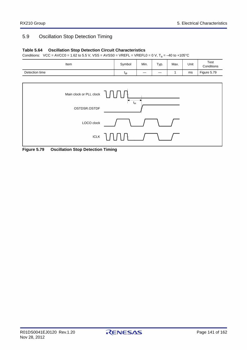
R01DS0041EJ0120 Rev.1.20 Page 141 of 162Nov 28, 2012
RX210 Group 5. Electrical Characteristics
5.9 Oscillation Stop Detection Timing
Figure 5.79 Oscillation Stop Detection Timing
Table 5.64 Oscillation Stop Detection Circuit CharacteristicsConditions: VCC = AVCC0 = 1.62 to 5.5 V, VSS = AVSS0 = VREFL = VREFL0 = 0 V, Ta = –40 to +105°C
Item Symbol Min. Typ. Max. UnitTest
Conditions
Detection time tdr — — 1 ms Figure 5.79
tdr
Main clock or PLL clock
OSTDSR.OSTDF
LOCO clock
ICLK
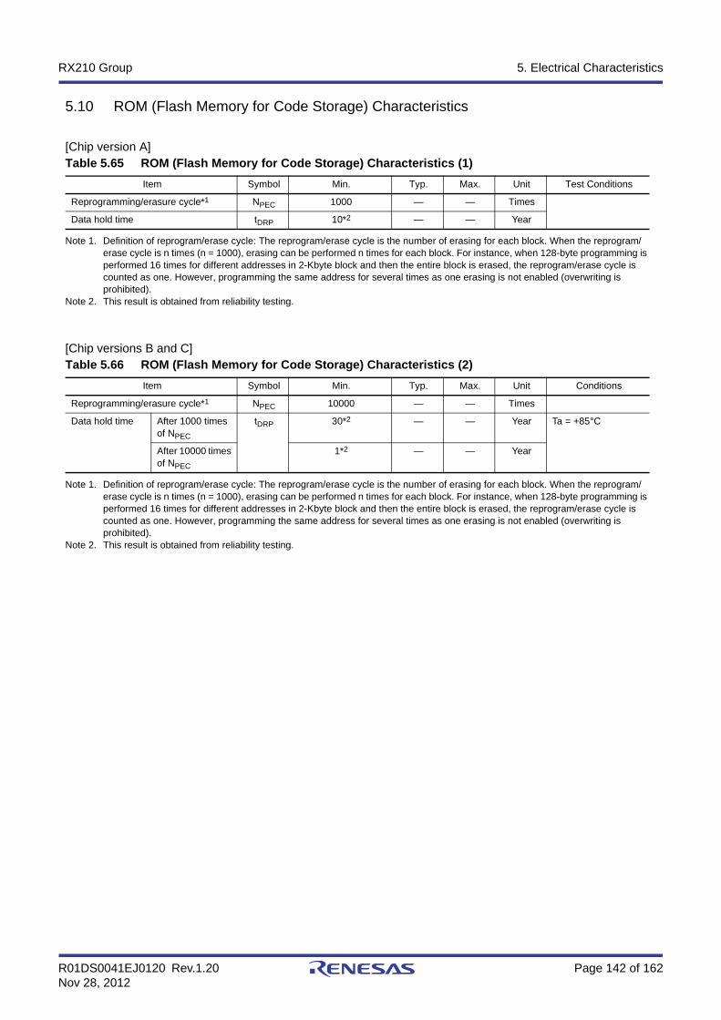
R01DS0041EJ0120 Rev.1.20 Page 142 of 162Nov 28, 2012
RX210 Group 5. Electrical Characteristics
5.10 ROM (Flash Memory for Code Storage) Characteristics
[Chip version A]
Note 1. Definition of reprogram/erase cycle: The reprogram/erase cycle is the number of erasing for each block. When the reprogram/erase cycle is n times (n = 1000), erasing can be performed n times for each block. For instance, when 128-byte programming is performed 16 times for different addresses in 2-Kbyte block and then the entire block is erased, the reprogram/erase cycle is counted as one. However, programming the same address for several times as one erasing is not enabled (overwriting is prohibited).
Note 2. This result is obtained from reliability testing.
[Chip versions B and C]
Note 1. Definition of reprogram/erase cycle: The reprogram/erase cycle is the number of erasing for each block. When the reprogram/erase cycle is n times (n = 1000), erasing can be performed n times for each block. For instance, when 128-byte programming is performed 16 times for different addresses in 2-Kbyte block and then the entire block is erased, the reprogram/erase cycle is counted as one. However, programming the same address for several times as one erasing is not enabled (overwriting is prohibited).
Note 2. This result is obtained from reliability testing.
Table 5.65 ROM (Flash Memory for Code Storage) Characteristics (1)
Item Symbol Min. Typ. Max. Unit Test Conditions
Reprogramming/erasure cycle*1 NPEC 1000 — — Times
Data hold time tDRP 10*2 — — Year
Table 5.66 ROM (Flash Memory for Code Storage) Characteristics (2)
Item Symbol Min. Typ. Max. Unit Conditions
Reprogramming/erasure cycle*1 NPEC 10000 — — Times
Data hold time After 1000 times of NPEC
tDRP 30*2 — — Year Ta = +85°C
After 10000 times of NPEC
1*2 — — Year

R01DS0041EJ0120 Rev.1.20 Page 143 of 162Nov 28, 2012
RX210 Group 5. Electrical Characteristics
[Chip versions A and C]Table 5.67 ROM (Flash Memory for Code Storage) Characteristics (3)
: high-speed operating mode, medium-speed operating mode 1AConditions: VCC = AVCC0 = 2.7 to 5.5 V, VREFH = VREFH0 = AVCC0, VSS = AVSS0 = VREFL = VREFL0 = 0 V
Temperature range for the programming/erasure operation: Ta = –40 to +105°C
Item SymbolFCLK = 4 MHz FCLK = 32 MHz
UnitMin. Typ. Max. Min. Typ. Max.
Programming timewhen NPEC ≤ 100 times
2 bytes tP2 — 0.52 4.8 — 0.19 2.5 ms
8 bytes tP8 — 0.52 4.9 — 0.19 2.5
128 bytes tP128 — 1.50 10.7 — 0.57 4.8
Programming timewhen NPEC > 100 times
2 bytes tP2 — 0.61 5.7 — 0.23 3.0 ms
8 bytes tP8 — 0.61 6.2 — 0.23 3.2
128 bytes tP128 — 1.71 13.2 — 0.65 6.0
Erasure timewhen NPEC ≤ 100 times
2 Kbytes tE2K — 17.0 92.9 — 11.0 29 ms
Erasure timewhen NPEC > 100 times
2 Kbytes tE2K — 20.8 195.8 — 13.5 60 ms
Suspend delay time during programming(in programming/erasure priority mode)
tSPD — — 0.9 — — 0.8 ms
First suspend delay time during programming (in suspend priority mode)
tSPSD1 — — 220 — — 120 μs
Second suspend delay time during programming (in suspend priority mode)
tSPSD2 — — 0.9 — — 0.8 ms
Suspend delay time during erasing (in programming/erasure priority mode)
tSED — — 0.9 — — 0.8 ms
First suspend delay time during erasing (in suspend priority mode)
tSESD1 — — 220 — — 120 μs
Second suspend delay time during erasing (in suspend priority mode)
tSESD2 — — 0.9 — — 0.8 ms
FCU reset time tFCUR 20 μs or longer and FCLK × 6
or greater
— — 20 μs or longer and FCLK × 6
or greater
— — μs

R01DS0041EJ0120 Rev.1.20 Page 144 of 162Nov 28, 2012
RX210 Group 5. Electrical Characteristics
[Chip versions A and C]
Note 1. The operating frequency is 20 MHz (max.) when the voltage is in the range from 1.62 V to less than 1.8 V.
Table 5.68 ROM (Flash Memory for Code Storage) Characteristics (4):medium-speed operating mode 1B
Conditions: VCC = AVCC0 = 1.62 to 3.6 V, VREFH = VREFH0 = AVCC0, VSS = AVSS0 = VREFL = VREFL0 = 0 VTemperature range for the programming/erasure operation: Ta = –40 to +105°C
Item SymbolFCLK = 4 MHz FCLK = 32 MHz*1
UnitMin. Typ. Max. Min. Typ. Max.
Programming timewhen NPEC ≤ 100 times
2 bytes tP2 — 0.69 6.0 — 0.30 3.5 ms
8 bytes tP8 — 0.69 6.0 — 0.30 3.5
128 bytes tP128 — 1.76 14.2 — 0.85 8.3
Programming timewhen NPEC > 100 times
2 bytes tP2 — 0.81 7.1 — 0.35 4.2 ms
8 bytes tP8 — 0.81 7.6 — 0.35 4.5
128 bytes tP128 — 1.99 17.5 — 0.96 10
Erasure timewhen NPEC ≤ 100 times
2 Kbytes tE2K — 24.5 113.7 — 19.0 46 ms
Erasure timewhen NPEC > 100 times
2 Kbytes tE2K — 29.8 225.8 — 23.2 90 (1000 times ≥ NPEC > 100 times), 98 (10000 times ≥
NPEC > 1000 times)
ms
Suspend delay time during programming(in programming/erasure priority mode)
tSPD — — 1.7 — — 1.6 ms
First suspend delay time during programming (in suspend priority mode)
tSPSD1 — — 220 — — 120 μs
Second suspend delay time during programming (in suspend priority mode)
tSPSD2 — — 1.7 — — 1.6 ms
Suspend delay time during erasing (in programming/erasure priority mode)
tSED — — 1.7 — — 1.6 ms
First suspend delay time during erasing (in suspend priority mode)
tSESD1 — — 220 — — 120 μs
Second suspend delay time during erasing (in suspend priority mode)
tSESD2 — — 1.7 — — 1.6 ms
FCU reset time tFCUR 20 μs or longer and FCLK × 6 or greater
— — 20 μs or longer and FCLK × 6 or greater
— — μs
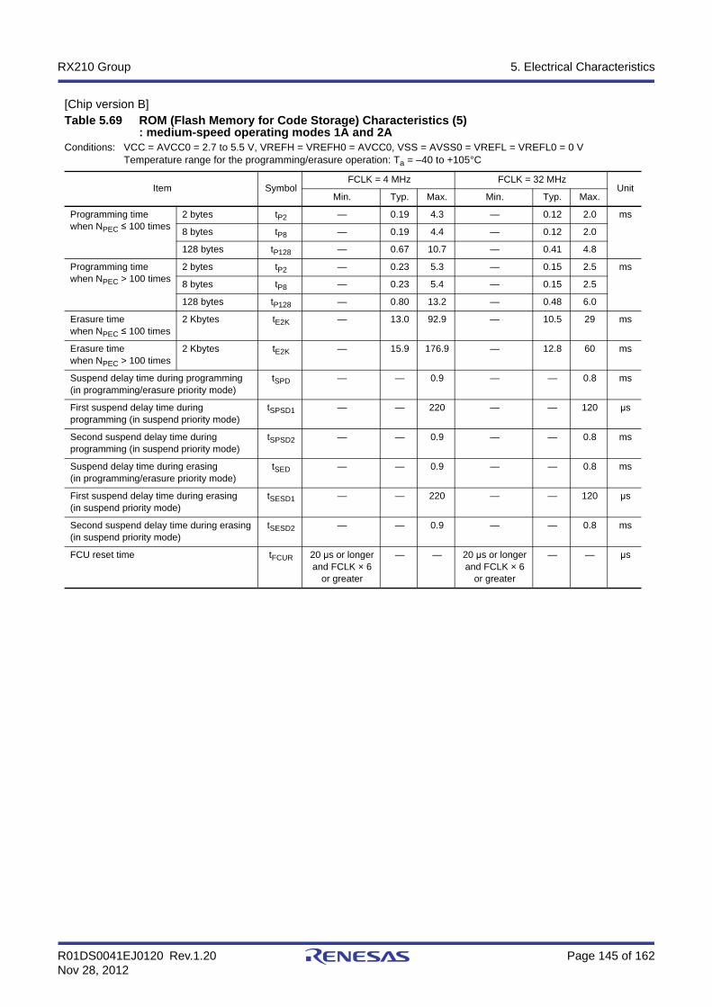
R01DS0041EJ0120 Rev.1.20 Page 145 of 162Nov 28, 2012
RX210 Group 5. Electrical Characteristics
[Chip version B]Table 5.69 ROM (Flash Memory for Code Storage) Characteristics (5)
: medium-speed operating modes 1A and 2AConditions: VCC = AVCC0 = 2.7 to 5.5 V, VREFH = VREFH0 = AVCC0, VSS = AVSS0 = VREFL = VREFL0 = 0 V
Temperature range for the programming/erasure operation: Ta = –40 to +105°C
Item SymbolFCLK = 4 MHz FCLK = 32 MHz
UnitMin. Typ. Max. Min. Typ. Max.
Programming timewhen NPEC ≤ 100 times
2 bytes tP2 — 0.19 4.3 — 0.12 2.0 ms
8 bytes tP8 — 0.19 4.4 — 0.12 2.0
128 bytes tP128 — 0.67 10.7 — 0.41 4.8
Programming timewhen NPEC > 100 times
2 bytes tP2 — 0.23 5.3 — 0.15 2.5 ms
8 bytes tP8 — 0.23 5.4 — 0.15 2.5
128 bytes tP128 — 0.80 13.2 — 0.48 6.0
Erasure timewhen NPEC ≤ 100 times
2 Kbytes tE2K — 13.0 92.9 — 10.5 29 ms
Erasure timewhen NPEC > 100 times
2 Kbytes tE2K — 15.9 176.9 — 12.8 60 ms
Suspend delay time during programming(in programming/erasure priority mode)
tSPD — — 0.9 — — 0.8 ms
First suspend delay time during programming (in suspend priority mode)
tSPSD1 — — 220 — — 120 μs
Second suspend delay time during programming (in suspend priority mode)
tSPSD2 — — 0.9 — — 0.8 ms
Suspend delay time during erasing (in programming/erasure priority mode)
tSED — — 0.9 — — 0.8 ms
First suspend delay time during erasing (in suspend priority mode)
tSESD1 — — 220 — — 120 μs
Second suspend delay time during erasing (in suspend priority mode)
tSESD2 — — 0.9 — — 0.8 ms
FCU reset time tFCUR 20 μs or longer and FCLK × 6
or greater
— — 20 μs or longer and FCLK × 6
or greater
— — μs
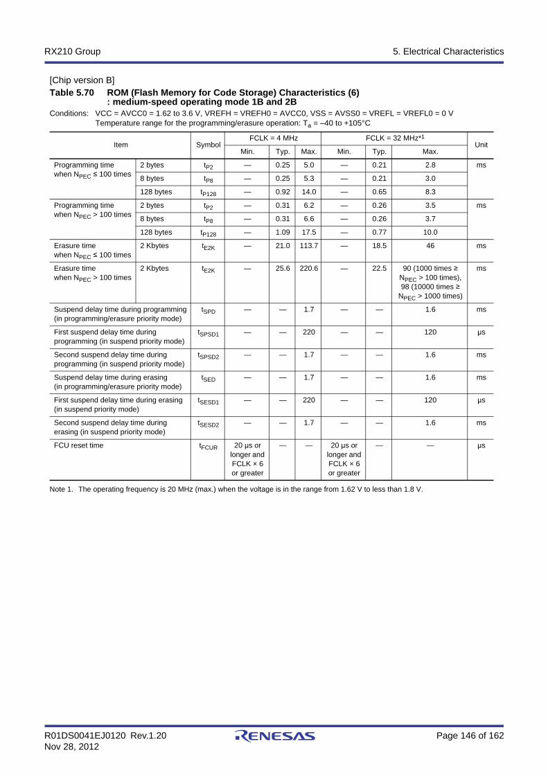
R01DS0041EJ0120 Rev.1.20 Page 146 of 162Nov 28, 2012
RX210 Group 5. Electrical Characteristics
[Chip version B]
Note 1. The operating frequency is 20 MHz (max.) when the voltage is in the range from 1.62 V to less than 1.8 V.
Table 5.70 ROM (Flash Memory for Code Storage) Characteristics (6): medium-speed operating mode 1B and 2B
Conditions: VCC = AVCC0 = 1.62 to 3.6 V, VREFH = VREFH0 = AVCC0, VSS = AVSS0 = VREFL = VREFL0 = 0 VTemperature range for the programming/erasure operation: Ta = –40 to +105°C
Item SymbolFCLK = 4 MHz FCLK = 32 MHz*1
UnitMin. Typ. Max. Min. Typ. Max.
Programming timewhen NPEC ≤ 100 times
2 bytes tP2 — 0.25 5.0 — 0.21 2.8 ms
8 bytes tP8 — 0.25 5.3 — 0.21 3.0
128 bytes tP128 — 0.92 14.0 — 0.65 8.3
Programming timewhen NPEC > 100 times
2 bytes tP2 — 0.31 6.2 — 0.26 3.5 ms
8 bytes tP8 — 0.31 6.6 — 0.26 3.7
128 bytes tP128 — 1.09 17.5 — 0.77 10.0
Erasure timewhen NPEC ≤ 100 times
2 Kbytes tE2K — 21.0 113.7 — 18.5 46 ms
Erasure timewhen NPEC > 100 times
2 Kbytes tE2K — 25.6 220.6 — 22.5 90 (1000 times ≥ NPEC > 100 times), 98 (10000 times ≥
NPEC > 1000 times)
ms
Suspend delay time during programming(in programming/erasure priority mode)
tSPD — — 1.7 — — 1.6 ms
First suspend delay time during programming (in suspend priority mode)
tSPSD1 — — 220 — — 120 μs
Second suspend delay time during programming (in suspend priority mode)
tSPSD2 — — 1.7 — — 1.6 ms
Suspend delay time during erasing (in programming/erasure priority mode)
tSED — — 1.7 — — 1.6 ms
First suspend delay time during erasing (in suspend priority mode)
tSESD1 — — 220 — — 120 μs
Second suspend delay time during erasing (in suspend priority mode)
tSESD2 — — 1.7 — — 1.6 ms
FCU reset time tFCUR 20 μs or longer and FCLK × 6 or greater
— — 20 μs or longer and FCLK × 6 or greater
— — μs

R01DS0041EJ0120 Rev.1.20 Page 147 of 162Nov 28, 2012
RX210 Group 5. Electrical Characteristics
5.11 E2 DataFlash Characteristics
[Chip version A]
Note 1. The reprogram/erase cycle is the number of erasing for each block. When the reprogram/erase cycle is n times (n = 100000), erasing can be performed n times for each block. For instance, when 8-byte programming is performed 16 times for different addresses in 128-byte block and then the entire block is erased, the reprogram/erase cycle is counted as one. However, programming the same address for several times as one erasing is not enabled (overwriting is prohibited).
Note 2. This result is obtained from reliability testing.
[Chip versions B and C]
Note 1. The reprogram/erase cycle is the number of erasing for each block. When the reprogram/erase cycle is n times (n = 100000), erasing can be performed n times for each block. For instance, when 8-byte programming is performed 16 times for different addresses in 128-byte block and then the entire block is erased, the reprogram/erase cycle is counted as one. However, programming the same address for several times as one erasing is not enabled (overwriting is prohibited).
Note 2. This result is obtained from reliability testing.
Table 5.71 E2 DataFlash Characteristics (1)
Item Symbol Min. Typ. Max. Unit Test Conditions
Reprogramming/erasure cycle*1 NDPEC 100000 — — Times
Data hold time tDRP 10*2 — — Year
Table 5.72 E2 DataFlash Characteristics (2)
Item Symbol Min. Typ. Max. Unit Test Conditions
Reprogramming/erasure cycle*1 NDPEC 100000 — — Times
Data hold time After 100000 times of NDPEC
tDRP 30*2 — — Year Ta = +85°C

R01DS0041EJ0120 Rev.1.20 Page 148 of 162Nov 28, 2012
RX210 Group 5. Electrical Characteristics
[Chip versions A and C]Table 5.73 E2 DataFlash Characteristics (3)
: high-speed operating mode, medium-speed operating mode 1AConditions: VCC = AVCC0 = 2.7 to 5.5 V, VREFH = VREFH0 = AVCC0, VSS = AVSS0 = VREFL = VREFL0 = 0 V
Temperature range for the programming/erasure operation: Ta = –40 to +105°C
Item SymbolFCLK = 4 MHz FCLK = 32 MHz
UnitMin. Typ. Max. Min. Typ. Max.
Programming timewhen NDPEC ≤ 100 times
2 bytes tDP2 — 0.40 4.4 — 0.16 2.0 ms
8 bytes tDP8 — 0.45 5.1 — 0.17 2.2
Programming timewhen NDPEC > 100 times
2 bytes tDP2 — 0.62 6.4 — 0.25 3.0 ms
8 bytes tDP8 — 0.69 7.5 — 0.26 3.2
Erasure timewhen NDPEC ≤ 100 times
128 bytes tDE128 — 5.6 27.1 — 2.8 8 ms
Erasure timewhen NDPEC > 100 times
128 bytes tDE128 — 6.8 45.1 — 3.4 12 ms
Blank check time 2 bytes tDBC2 — — 98 — — 35 μs
2 Kbytes tDBC2K — — 16 — — 2.5 ms
Suspend delay time during programming (in programming/erasure priority mode)
tDSPD — — 0.9 — — 0.8 ms
First suspend delay time during programming (in suspend priority mode)
tDSPSD1 — — 220 — — 120 μs
Second suspend delay time during programming (in suspend priority mode)
tDSPSD2 — — 0.9 — — 0.8 ms
Suspend delay time during erasing (in programming/erasure priority mode)
tDSED — — 0.9 — — 0.8 ms
First suspend delay time during erasing (in suspend priority mode)
tDSESD1 — — 220 — — 120 μs
Second suspend delay time during erasing (in suspend priority mode)
tDSESD2 — — 0.9 — — 0.8 ms
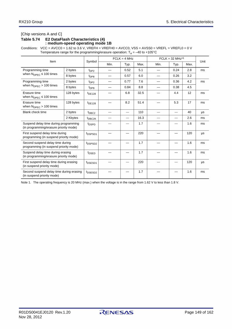
R01DS0041EJ0120 Rev.1.20 Page 149 of 162Nov 28, 2012
RX210 Group 5. Electrical Characteristics
[Chip versions A and C]
Note 1. The operating frequency is 20 MHz (max.) when the voltage is in the range from 1.62 V to less than 1.8 V.
Table 5.74 E2 DataFlash Characteristics (4): medium-speed operating mode 1B
Conditions: VCC = AVCC0 = 1.62 to 3.6 V, VREFH = VREFH0 = AVCC0, VSS = AVSS0 = VREFL = VREFL0 = 0 VTemperature range for the programming/erasure operation: Ta = –40 to +105°C
Item SymbolFCLK = 4 MHz FCLK = 32 MHz*1
UnitMin. Typ. Max. Min. Typ. Max.
Programming timewhen NDPEC ≤ 100 times
2 bytes tDP2 — 0.52 5.1 — 0.24 2.8 ms
8 bytes tDP8 — 0.57 6.0 — 0.26 3.2
Programming timewhen NDPEC > 100 times
2 bytes tDP2 — 0.77 7.6 — 0.36 4.2 ms
8 bytes tDP8 — 0.84 8.8 — 0.38 4.5
Erasure timewhen NDPEC ≤ 100 times
128 bytes tDE128 — 6.8 32.5 — 4.4 12 ms
Erasure timewhen NDPEC > 100 times
128 bytes tDE128 — 8.2 51.4 — 5.3 17 ms
Blank check time 2 bytes tDBC2 — — 110 — — 40 μs
2 Kbytes tDBC2K — — 16.3 — — 2.6 ms
Suspend delay time during programming (in programming/erasure priority mode)
tDSPD — — 1.7 — — 1.6 ms
First suspend delay time during programming (in suspend priority mode)
tDSPSD1 — — 220 — — 120 μs
Second suspend delay time during programming (in suspend priority mode)
tDSPSD2 — — 1.7 — — 1.6 ms
Suspend delay time during erasing (in programming/erasure priority mode)
tDSED — — 1.7 — — 1.6 ms
First suspend delay time during erasing (in suspend priority mode)
tDSESD1 — — 220 — — 120 μs
Second suspend delay time during erasing (in suspend priority mode)
tDSESD2 — — 1.7 — — 1.6 ms
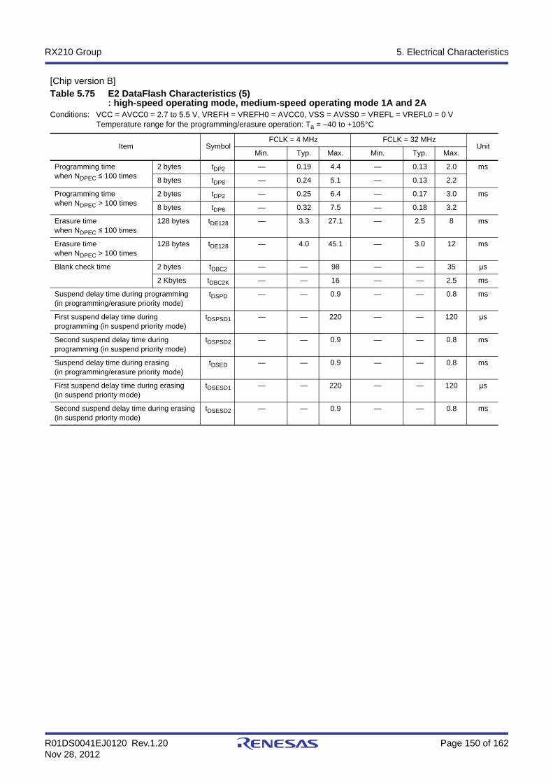
R01DS0041EJ0120 Rev.1.20 Page 150 of 162Nov 28, 2012
RX210 Group 5. Electrical Characteristics
[Chip version B]Table 5.75 E2 DataFlash Characteristics (5)
: high-speed operating mode, medium-speed operating mode 1A and 2AConditions: VCC = AVCC0 = 2.7 to 5.5 V, VREFH = VREFH0 = AVCC0, VSS = AVSS0 = VREFL = VREFL0 = 0 V
Temperature range for the programming/erasure operation: Ta = –40 to +105°C
Item SymbolFCLK = 4 MHz FCLK = 32 MHz
UnitMin. Typ. Max. Min. Typ. Max.
Programming timewhen NDPEC ≤ 100 times
2 bytes tDP2 — 0.19 4.4 — 0.13 2.0 ms
8 bytes tDP8 — 0.24 5.1 — 0.13 2.2
Programming timewhen NDPEC > 100 times
2 bytes tDP2 — 0.25 6.4 — 0.17 3.0 ms
8 bytes tDP8 — 0.32 7.5 — 0.18 3.2
Erasure timewhen NDPEC ≤ 100 times
128 bytes tDE128 — 3.3 27.1 — 2.5 8 ms
Erasure timewhen NDPEC > 100 times
128 bytes tDE128 — 4.0 45.1 — 3.0 12 ms
Blank check time 2 bytes tDBC2 — — 98 — — 35 μs
2 Kbytes tDBC2K — — 16 — — 2.5 ms
Suspend delay time during programming (in programming/erasure priority mode)
tDSPD — — 0.9 — — 0.8 ms
First suspend delay time during programming (in suspend priority mode)
tDSPSD1 — — 220 — — 120 μs
Second suspend delay time during programming (in suspend priority mode)
tDSPSD2 — — 0.9 — — 0.8 ms
Suspend delay time during erasing (in programming/erasure priority mode)
tDSED — — 0.9 — — 0.8 ms
First suspend delay time during erasing (in suspend priority mode)
tDSESD1 — — 220 — — 120 μs
Second suspend delay time during erasing (in suspend priority mode)
tDSESD2 — — 0.9 — — 0.8 ms

R01DS0041EJ0120 Rev.1.20 Page 151 of 162Nov 28, 2012
RX210 Group 5. Electrical Characteristics
[Chip version B]
Note 1. The operating frequency is 20 MHz (max.) when the voltage is in the range from 1.62 V to less than 1.8 V.
Table 5.76 E2 DataFlash Characteristics (6): medium-speed operating mode 1B and 2B
Conditions: VCC = AVCC0 = 1.62 to 3.6 V, VREFH = VREFH0 = AVCC0, VSS = AVSS0 = VREFL = VREFL0 = 0 VTemperature range for the programming/erasure operation: Ta = –40 to +105°C
Item SymbolFCLK = 4 MHz FCLK = 32 MHz*1
UnitMin. Typ. Max. Min. Typ. Max.
Programming timewhen NDPEC ≤ 100 times
2 bytes tDP2 — 0.28 5.1 — 0.20 2.8 ms
8 bytes tDP8 — 0.32 6.0 — 0.22 3.2
Programming timewhen NDPEC > 100 times
2 bytes tDP2 — 0.36 7.6 — 0.25 4.2 ms
8 bytes tDP8 — 0.40 8.8 — 0.28 4.5
Erasure timewhen NDPEC ≤ 100 times
128 bytes tDE128 — 4.8 32.4 — 4.1 12 ms
Erasure timewhen NDPEC > 100 times
128 bytes tDE128 — 5.8 51.4 — 4.9 17 ms
Blank check time 2 bytes tDBC2 — — 110 — — 40 μs
2 Kbytes tDBC2K — — 16.3 — — 2.6 ms
Suspend delay time during programming (in programming/erasure priority mode)
tDSPD — — 1.7 — — 1.6 ms
First suspend delay time during programming (in suspend priority mode)
tDSPSD1 — — 220 — — 120 μs
Second suspend delay time during programming (in suspend priority mode)
tDSPSD2 — — 1.7 — — 1.6 ms
Suspend delay time during erasing (in programming/erasure priority mode)
tDSED — — 1.7 — — 1.6 ms
First suspend delay time during erasing (in suspend priority mode)
tDSESD1 — — 220 — — 120 μs
Second suspend delay time during erasing (in suspend priority mode)
tDSESD2 — — 1.7 — — 1.6 ms
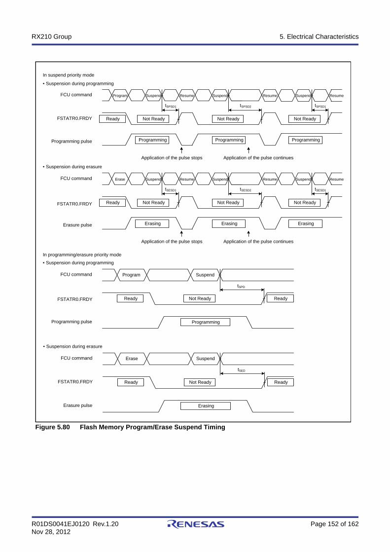
R01DS0041EJ0120 Rev.1.20 Page 152 of 162Nov 28, 2012
RX210 Group 5. Electrical Characteristics
Figure 5.80 Flash Memory Program/Erase Suspend Timing
• Suspension during erasure
FCU command
FSTATR0.FRDY
Programming pulse
• Suspension during programming
Program Suspend
Ready Not Ready Ready
tSPD
Programming
FCU command
FSTATR0.FRDY
Programming pulse
• Suspension during programming
Ready Not Ready Not Ready
tSPSD1
FCU command
FSTATR0.FRDY
Erasure pulse
• Suspension during erasure
Erase Suspend
Ready Not Ready Ready
tSED
Erasing
In suspend priority mode
In programming/erasure priority mode
Program Suspend Resume Suspend Resume Suspend Resume
tSPSD2
Not Ready
tSPSD1
Programming ProgrammingProgramming
Application of the pulse stops Application of the pulse continues
FCU command
Erasure pulse
Ready Not Ready Not Ready
tSESD1
Erase Suspend Resume Suspend Resume Suspend Resume
tSESD2
Not Ready
tSESD1
Erasing ErasingErasing
Application of the pulse stops Application of the pulse continues
FSTATR0.FRDY

R01DS0041EJ0120 Rev.1.20 Page 153 of 162Nov 28, 2012
RX210 Group Appendix 1. Package Dimensions
Appendix 1. Package DimensionsInformation on the latest version of the package dimensions or mountings has been displayed in “Packages” on Renesas
Electronics Corporation website.
Figure A 100-Pin TFLGA (PTLG0100JA-A)
P-TFLGA100-7x7-0.65 0.1g
MASS[Typ.]
100F0GPTLG0100JA-A
RENESAS CodeJEITA Package Code Previous Code
0.15v
0.20w
0.08
0.4850.4350.385
MaxNomMin
Dimension in MillimetersSymbol
Reference
7.0D
7.0E
1.05A
x
0.65e
0.10y
b1
b 0.31 0.35 0.39
0.575ZD
ZE 0.575
Index mark
Bw
Sw AS
A
H
G
F
E
D
C
B
1 2 3 4 5 6 7 8y S
S
A
v
×4
(Laser mark)
Index mark
J
K
9 10
D
E
e
e
A ZD
ZE
B
φ b
φ b1
φ× M S AB
φ× M S AB
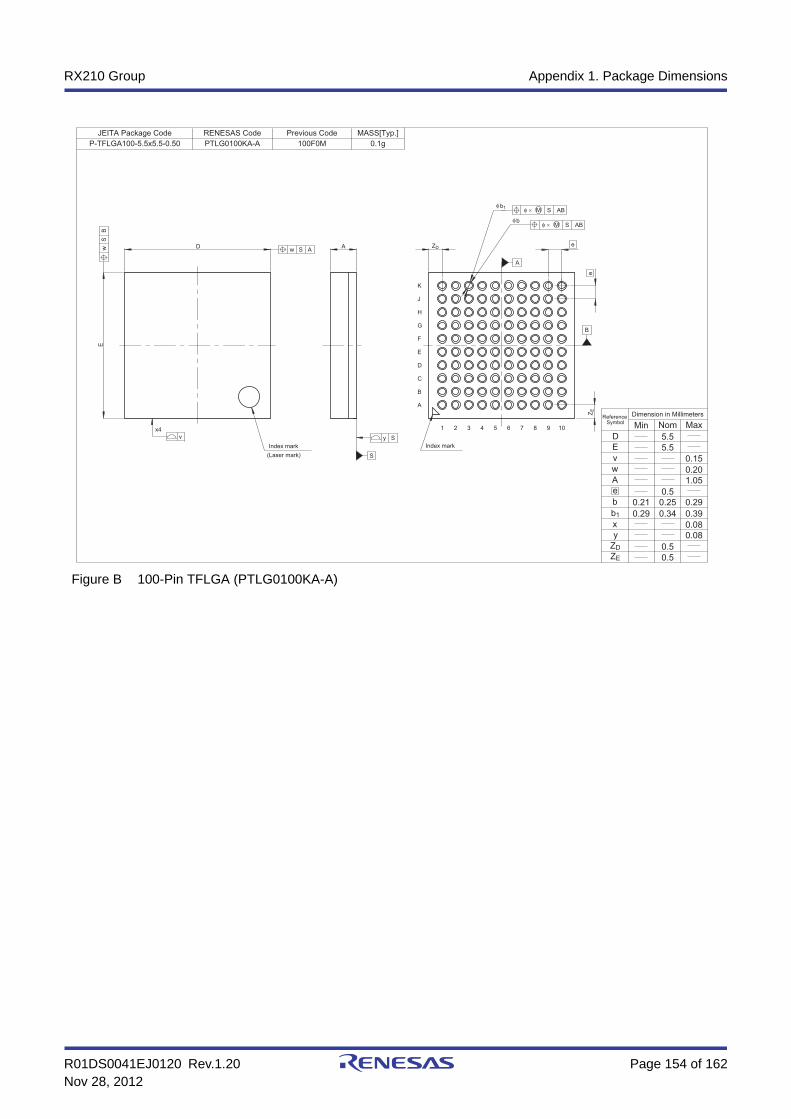
R01DS0041EJ0120 Rev.1.20 Page 154 of 162Nov 28, 2012
RX210 Group Appendix 1. Package Dimensions
Figure B 100-Pin TFLGA (PTLG0100KA-A)e
e
A
B
C
D
E
F
G
H
J
K
1 2 3 4 5 6 7 8 9 10
B
A
S
y S
Index mark Index mark
(Laser mark)
x4
v
Aw S
Bw
S
D
E
ZD
ZE
A
S ABMφ ×
S ABMφ ×
φb1
φb
0.15
1.05
0.08
0.08
ReferenceSymbol
Dimension in Millimeters
Min Nom Max
D
E
v
ZD
b1
b
5.5
5.5
0.5
0.5
A
0.5e
w
x
y
ZE
0.20
0.250.21 0.29
0.340.29 0.39
P-TFLGA100-5.5x5.5-0.50 0.1g
MASS[Typ.]
100F0MPTLG0100KA-A
RENESAS CodeJEITA Package Code Previous Code

R01DS0041EJ0120 Rev.1.20 Page 155 of 162Nov 28, 2012
RX210 Group Appendix 1. Package Dimensions
Figure C 64-Pin TFLGA (PTLG0064JA-A)
0.15v
0.20w
Previous CodeJEITA Package Code RENESAS Code
PTLG0064JA-A 64F0G
MASS[Typ.]
0.07gP-TFLGA64-6x6-0.65
0.08
0.470.430.39
MaxNomMin
Dimension in MillimetersSymbolReference
6.0D
6.0E
1.05A
x
0.65e
0.10y
b1
b 0.31 0.35 0.39
Bw
Sw AS
A
H
G
F
E
D
C
B
1 2 3 4 5 6 7 8
S
y S
AB
Index mark
S AB
v
x4
(Laser mark)
Index mark
D
E
A
b1
b
e
e
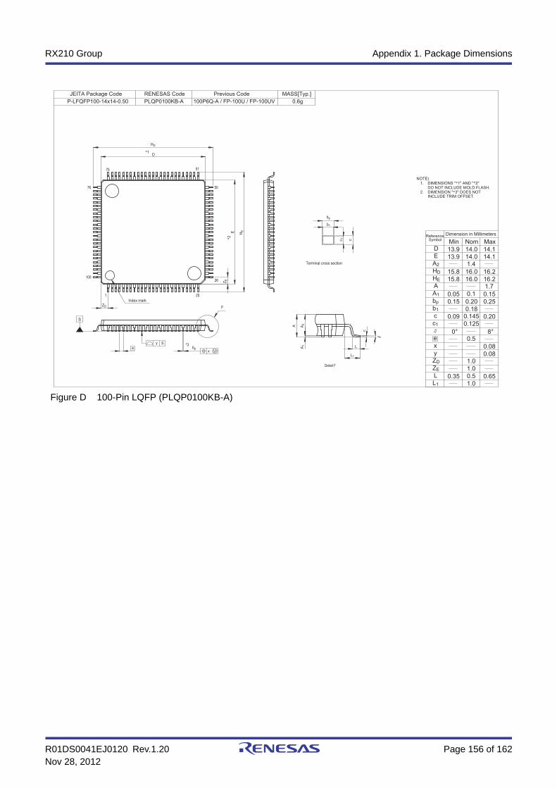
R01DS0041EJ0120 Rev.1.20 Page 156 of 162Nov 28, 2012
RX210 Group Appendix 1. Package Dimensions
Figure D 100-Pin LQFP (PLQP0100KB-A)
Terminal cross section
b1
c 1
bp
c
2.
1. DIMENSIONS "*1" AND "*2"DO NOT INCLUDE MOLD FLASH.
NOTE)
DIMENSION "*3" DOES NOTINCLUDE TRIM OFFSET.
Index mark
x
1 25
26
50
5175
76
100
F
*1
*3
*2
ZE
ZD
E
D
HD
HE
bp
Detail F
L1
A2
A1 L
A
c
L1
ZE
ZD
c1
b1
bp
A1
HE
HD
y 0.08
e 0.5
c
0° 8°
x
L 0.35 0.5 0.65
0.05 0.1 0.15
A 1.715.8 16.0 16.2
15.8 16.0 16.2
A2 1.4
E 13.9 14.0 14.1
D 13.9 14.0 14.1
ReferenceSymbol
Dimension in Millimeters
Min Nom Max
0.15 0.20 0.25
0.09 0.145 0.20
0.08
1.0
1.0
0.18
0.125
1.0
Previous CodeJEITA Package Code RENESAS Code
PLQP0100KB-A 100P6Q-A / FP-100U / FP-100UV
MASS[Typ.]
0.6gP-LFQFP100-14x14-0.50
e
y S
S
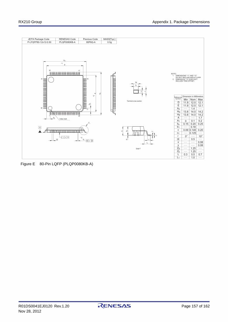
R01DS0041EJ0120 Rev.1.20 Page 157 of 162Nov 28, 2012
RX210 Group Appendix 1. Package Dimensions
Figure E 80-Pin LQFP (PLQP0080KB-A)
Detail F
cA
L1
LA1
A2
Index mark
*2
*1
*3
F
80
61
60 41
40
21
201
x
ZE
ZD
E HE
D
HD
e bp
2.
1. DIMENSIONS "*1" AND "*2"DO NOT INCLUDE MOLD FLASH.
NOTE)
DIMENSION "*3" DOES NOTINCLUDE TRIM OFFSET.
Previous CodeJEITA Package Code RENESAS Code
PLQP0080KB-A 80P6Q-A
MASS[Typ.]
0.5gP-LFQFP80-12x12-0.50
1.0
0.125
0.18
1.25
1.25
0.08
0.200.1450.09
0.250.200.15
MaxNomMin
Dimension in MillimetersSymbolReference
12.112.011.9D
12.112.011.9E
1.4A214.214.013.8
14.214.013.8
1.7A
0.20.10
0.70.50.3L
x
10°0°
c
0.5e
0.08y
HDHE
A1bpb1
c1
ZDZE
L1
Terminal cross section
c
bp
c 1
b1
y S
S

R01DS0041EJ0120 Rev.1.20 Page 158 of 162Nov 28, 2012
RX210 Group Appendix 1. Package Dimensions
Figure F 80-Pin LQFP (PLQP0080JA-A)
L1
ZE
ZD
c1
b1
bp
A1
HE
HD
y 0.10
e 0.65
c
0° 8°
x
L 0.35 0.5 0.65
0.05 0.1 0.15
A 1.7
15.8 16.0 16.2
15.8 16.0 16.2
A2 1.4
E 13.9 14.0 14.1
D 13.9 14.0 14.1
ReferenceSymbol
Dimension in Millimeters
Min Nom Max
0.27 0.32 0.37
0.09 0.145 0.20
0.13
0.825
0.825
0.30
0.125
1.0
P-LQFP80-14x14-0.65 0.6g
MASS[Typ.]
FP-80W / FP-80WVPLQP0080JA-A
RENESAS CodeJEITA Package Code Previous Code
INCLUDE TRIM OFFSET.DIMENSION "*3" DOES NOT
NOTE)
DO NOT INCLUDE MOLD FLASH.DIMENSIONS "*1" AND "*2"1.
2.
c1 c
bp
b1
Terminal cross section
A2
c
L
A1
A
L1
Detail F
ZE
ZD
HE
HD
D
E*2
*1
*3
F
80
61
60 41
40
21
201
Index mark
e bp× M
θ
θS
y S
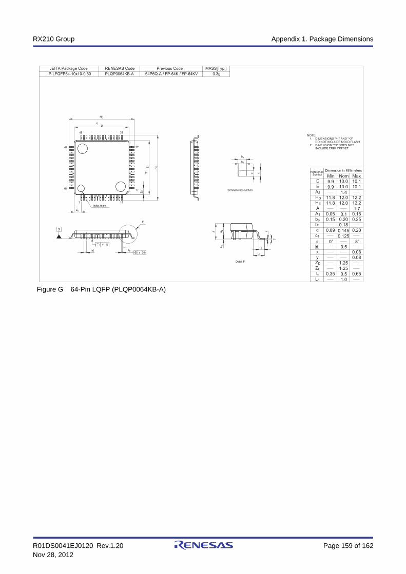
R01DS0041EJ0120 Rev.1.20 Page 159 of 162Nov 28, 2012
RX210 Group Appendix 1. Package Dimensions
Figure G 64-Pin LQFP (PLQP0064KB-A)
Terminal cross section
b1
c 1
bp
c
2.
1. DIMENSIONS "*1" AND "*2"DO NOT INCLUDE MOLD FLASH.
NOTE)
DIMENSION "*3" DOES NOTINCLUDE TRIM OFFSET.
Index mark
*3
17
32
64
49
1 16
3348
F
*1
*2
xbp
HEE
HD
D
ZD
ZE
Detail F
A cA2
A1
L1
L
P-LFQFP64-10x10-0.50 0.3g
MASS[Typ.]
64P6Q-A / FP-64K / FP-64KVPLQP0064KB-A
RENESAS CodeJEITA Package Code Previous Code
1.0
0.125
0.18
1.25
1.25
0.08
0.200.1450.09
0.250.200.15
MaxNomMin
Dimension in MillimetersSymbol
Reference
10.110.09.9D
10.110.09.9E
1.4A212.212.011.8
12.212.011.8
1.7A
0.150.10.05
0.650.50.35L
x
8°0°
c
0.5e
0.08y
HDHE
A1bpb1
c1
ZDZE
L1
e
y S
S

R01DS0041EJ0120 Rev.1.20 Page 160 of 162Nov 28, 2012
RX210 Group Appendix 1. Package Dimensions
Figure H 64-Pin LQFP (PLQP0064GA-A)
Terminal cross section
b1
c1
bp
c
2.
1. DIMENSIONS "*1" AND "*2"DO NOT INCLUDE MOLD FLASH.
NOTE)
DIMENSION "*3" DOES NOTINCLUDE TRIM OFFSET.
*3
1 16
17
32
3348
49
64
F
*1
*2
x
Index mark
D
HD
E H E
e bp
ZD
Z E
Detail F
cA A 2A 1 L
L1
Previous CodeJEITA Package Code RENESAS CodePLQP0064GA-A 64P6U-A/ ⎯
MASS[Typ.]0.7gP-LQFP64-14x14-0.80
1.0
0.125
0.35
1.01.0
0.20
0.200.1450.09
0.420.370.32
MaxNomMinDimension in Millimeters
SymbolReference
14.114.013.9D14.114.013.9E
1.4A216.216.015.816.216.015.81.7A0.20.10
0.70.50.3L
x
8°0°
c
0.8e
0.10y
HDHE
A1bpb1
c1
ZDZE
L1
y S
S
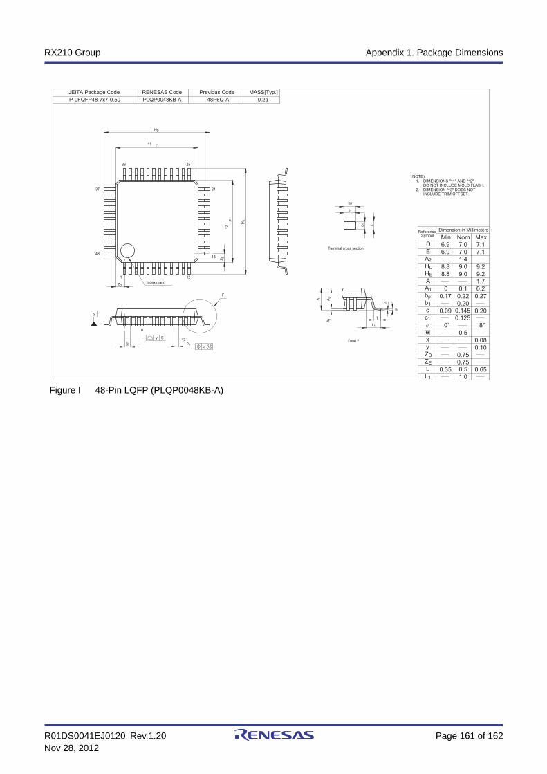
R01DS0041EJ0120 Rev.1.20 Page 161 of 162Nov 28, 2012
RX210 Group Appendix 1. Package Dimensions
Figure I 48-Pin LQFP (PLQP0048KB-A)
Terminal cross section
b1
c 1
bp
c
2.
1. DIMENSIONS "*1" AND "*2"DO NOT INCLUDE MOLD FLASH.
NOTE)
DIMENSION "*3" DOES NOTINCLUDE TRIM OFFSET.
Detail F
L1
c
AL
A1
A2
*3
F
48
37
36 25
24
13
121
*1
*2
x
Index mark
ZE
ZD
bpe
HE
HD
D
E
Previous CodeJEITA Package Code RENESAS Code
PLQP0048KB-A 48P6Q-A
MASS[Typ.]
0.2gP-LFQFP48-7x7-0.50
1.0
0.125
0.20
0.75
0.75
0.08
0.200.1450.09
0.270.220.17
MaxNomMin
Dimension in MillimetersSymbol
Reference
7.17.06.9D
7.17.06.9E
1.4A2
9.29.08.8
9.29.08.8
1.7A
0.20.10
0.650.50.35L
x
8°0°
c
0.5e
0.10y
HD
HE
A1
bp
b1
c1
ZD
ZE
L1
y S
S

R01DS0041EJ0120 Rev.1.20 Page 162 of 162Nov 28, 2012
RX210 Group REVISION HISTORY
REVISION HISTORY RX210 Group Datasheet
Rev. DateDescription
Page Summary
0.50 Apr.15, 2011 — First edition, issued
0.90 Aug.10, 2011 1. Overview
4 Table 1.1 Outline of Specifications: Power supply voltage/ Operating frequency, changed
17, 21, 24, 26
Table 1.5 to Table 1.8 List of Pins and Pin Functions (Pin name: LVCMP2 CMPA2), changed
2. CPU
51 Table 2.14 Instructions that are Converted into Multiple Micro-Operations (multiplier: 32 × 32 64 bits), (memory source operand), added
4. I/O Registers
63 Table 5.1 List of I/O Registers (Address Order), SOSCWTCR, LOCOWTCR2, HOCOWTCR2, added
114 to 116 Table 5.1 List of I/O Registers (Address Order): Interrupt source priority register, changed
5. Electrical Characteristics
85 to 137 Newly added
1.20 Nov 28, 2012 All Information on chip versions A, B, and C, corresponding descriptions and notes, added48-pin products added, PLQP0080JA-A 14 14 mm, 0.65-mm pitch, package deleted
Features
1 Description changed
1. Overview
2 1.1 Outline of Specifications: Description, changed
2 to 5 Table 1.1 Outline of Specifications, changedNote 1, added
6 Table 1.2 Comparison of Functions for Different Packages, changed
7 Table 1.3 List of Products, changed
8 to 10 Tables 1.4 to 1.7 List of Products, added
11 Figure 1.1 How to Read the Product Part No., Memory Capacity, and Package Type: G item added
12 Figure 1.2 Block Diagram, changed
13 Table 1.8 Pin Functions: Power supply and On-chip emulator, changed
13 Table 1.8 Pin Functions: Multiplexed bus, added
18 Figure 1.4 Pin Assignments of the 100-Pin LQFP, changed
21 Figure 1.7 Pin Assignments of the 48-Pin LQFP, added
23 Table 1.9 List of Pins and Pin Functions (100-Pin TFLGA): Pin No. G4, changed
25 Table 1.10 List of Pins and Pin Functions (100-Pin LQFP): Pin No. 21, changed
28 Table 1.11 List of Pins and Pin Functions (80-Pin LQFP): Pin No. 19, changed
30 Table 1.12 List of Pins and Pin Functions (64-Pin LQFP): Pin No. 15, changed
3. Address Space
37 Figure 3.1 Memory Map in Each Operating Mode: Note 2, changed
4. I/O Registers
41 to 63 Table 4.1 List of I/O Registers (Address Order): Number of Access, changedVoltage regulator control register, Timeout internal counter L, Timeout internal counter U, and PLLpower control register, added
63 Table 4.1 List of I/O Registers (Address Order): Notes 1 and 2, added
— Table 4.1 List of I/O Registers (Address Order): LOCO Wait Control Register 2 (LOCOWTCR2), deleted
5. Electrical Characteristics
64 to 152 Description added
REVISION HISTORY

General Precautions in the Handling of MPU/MCU Products
The following usage notes are applicable to all MPU/MCU products from Renesas. For detailed usage notes on the products covered by this manual, refer to the relevant sections of the manual. If the descriptions under General Precautions in the Handling of MPU/MCU Products and in the body of the manual differ from each other, the description in the body of the manual takes precedence.
1. Handling of Unused Pins Handle unused pins in accord with the directions given under Handling of Unused Pins in the manual. The input pins of CMOS products are generally in the high-impedance state. In operation
with an unused pin in the open-circuit state, extra electromagnetic noise is induced in the vicinity of LSI, an associated shoot-through current flows internally, and malfunctions occur due to the false recognition of the pin state as an input signal become possible. Unused pins should be handled as described under Handling of Unused Pins in the manual.
2. Processing at Power-on The state of the product is undefined at the moment when power is supplied. The states of internal circuits in the LSI are indeterminate and the states of register
settings and pins are undefined at the moment when power is supplied. In a finished product where the reset signal is applied to the external reset pin, the states of pins are not guaranteed from the moment when power is supplied until the reset process is completed. In a similar way, the states of pins in a product that is reset by an on-chip power-on reset function are not guaranteed from the moment when power is supplied until the power reaches the level at which resetting has been specified.
3. Prohibition of Access to Reserved Addresses Access to reserved addresses is prohibited. The reserved addresses are provided for the possible future expansion of functions. Do
not access these addresses; the correct operation of LSI is not guaranteed if they are accessed.
4. Clock Signals After applying a reset, only release the reset line after the operating clock signal has become stable. When switching the clock signal during program execution, wait until the target clock signal has stabilized. When the clock signal is generated with an external resonator (or from an external
oscillator) during a reset, ensure that the reset line is only released after full stabilization of the clock signal. Moreover, when switching to a clock signal produced with an external resonator (or by an external oscillator) while program execution is in progress, wait until the target clock signal is stable.
5. Differences between Products Before changing from one product to another, i.e. to one with a different part number, confirm that the change will not lead to problems. The characteristics of MPU/MCU in the same group but having different part numbers may
differ because of the differences in internal memory capacity and layout pattern. When changing to products of different part numbers, implement a system-evaluation test for each of the products.

Notice1. Descriptions of circuits, software and other related information in this document are provided only to illustrate the operation of semiconductor products and application examples. You are fully responsible for
the incorporation of these circuits, software, and information in the design of your equipment. Renesas Electronics assumes no responsibility for any losses incurred by you or third parties arising from the
use of these circuits, software, or information.
2. Renesas Electronics has used reasonable care in preparing the information included in this document, but Renesas Electronics does not warrant that such information is error free. Renesas Electronics
assumes no liability whatsoever for any damages incurred by you resulting from errors in or omissions from the information included herein.
3. Renesas Electronics does not assume any liability for infringement of patents, copyrights, or other intellectual property rights of third parties by or arising from the use of Renesas Electronics products or
technical information described in this document. No license, express, implied or otherwise, is granted hereby under any patents, copyrights or other intellectual property rights of Renesas Electronics or
others.
4. You should not alter, modify, copy, or otherwise misappropriate any Renesas Electronics product, whether in whole or in part. Renesas Electronics assumes no responsibility for any losses incurred by you or
third parties arising from such alteration, modification, copy or otherwise misappropriation of Renesas Electronics product.
5. Renesas Electronics products are classified according to the following two quality grades: "Standard" and "High Quality". The recommended applications for each Renesas Electronics product depends on
the product's quality grade, as indicated below.
"Standard": Computers; office equipment; communications equipment; test and measurement equipment; audio and visual equipment; home electronic appliances; machine tools; personal electronic
equipment; and industrial robots etc.
"High Quality": Transportation equipment (automobiles, trains, ships, etc.); traffic control systems; anti-disaster systems; anti-crime systems; and safety equipment etc.
Renesas Electronics products are neither intended nor authorized for use in products or systems that may pose a direct threat to human life or bodily injury (artificial life support devices or systems, surgical
implantations etc.), or may cause serious property damages (nuclear reactor control systems, military equipment etc.). You must check the quality grade of each Renesas Electronics product before using it
in a particular application. You may not use any Renesas Electronics product for any application for which it is not intended. Renesas Electronics shall not be in any way liable for any damages or losses
incurred by you or third parties arising from the use of any Renesas Electronics product for which the product is not intended by Renesas Electronics.
6. You should use the Renesas Electronics products described in this document within the range specified by Renesas Electronics, especially with respect to the maximum rating, operating supply voltage
range, movement power voltage range, heat radiation characteristics, installation and other product characteristics. Renesas Electronics shall have no liability for malfunctions or damages arising out of the
use of Renesas Electronics products beyond such specified ranges.
7. Although Renesas Electronics endeavors to improve the quality and reliability of its products, semiconductor products have specific characteristics such as the occurrence of failure at a certain rate and
malfunctions under certain use conditions. Further, Renesas Electronics products are not subject to radiation resistance design. Please be sure to implement safety measures to guard them against the
possibility of physical injury, and injury or damage caused by fire in the event of the failure of a Renesas Electronics product, such as safety design for hardware and software including but not limited to
redundancy, fire control and malfunction prevention, appropriate treatment for aging degradation or any other appropriate measures. Because the evaluation of microcomputer software alone is very difficult,
please evaluate the safety of the final products or systems manufactured by you.
8. Please contact a Renesas Electronics sales office for details as to environmental matters such as the environmental compatibility of each Renesas Electronics product. Please use Renesas Electronics
products in compliance with all applicable laws and regulations that regulate the inclusion or use of controlled substances, including without limitation, the EU RoHS Directive. Renesas Electronics assumes
no liability for damages or losses occurring as a result of your noncompliance with applicable laws and regulations.
9. Renesas Electronics products and technology may not be used for or incorporated into any products or systems whose manufacture, use, or sale is prohibited under any applicable domestic or foreign laws or
regulations. You should not use Renesas Electronics products or technology described in this document for any purpose relating to military applications or use by the military, including but not limited to the
development of weapons of mass destruction. When exporting the Renesas Electronics products or technology described in this document, you should comply with the applicable export control laws and
regulations and follow the procedures required by such laws and regulations.
10. It is the responsibility of the buyer or distributor of Renesas Electronics products, who distributes, disposes of, or otherwise places the product with a third party, to notify such third party in advance of the
contents and conditions set forth in this document, Renesas Electronics assumes no responsibility for any losses incurred by you or third parties as a result of unauthorized use of Renesas Electronics
products.
11. This document may not be reproduced or duplicated in any form, in whole or in part, without prior written consent of Renesas Electronics.
12. Please contact a Renesas Electronics sales office if you have any questions regarding the information contained in this document or Renesas Electronics products, or if you have any other inquiries.
(Note 1) "Renesas Electronics" as used in this document means Renesas Electronics Corporation and also includes its majority-owned subsidiaries.
(Note 2) "Renesas Electronics product(s)" means any product developed or manufactured by or for Renesas Electronics.
http://www.renesas.comRefer to "http://www.renesas.com/" for the latest and detailed information.
Renesas Electronics America Inc. 2880 Scott Boulevard Santa Clara, CA 95050-2554, U.S.A.Tel: +1-408-588-6000, Fax: +1-408-588-6130Renesas Electronics Canada Limited1101 Nicholson Road, Newmarket, Ontario L3Y 9C3, CanadaTel: +1-905-898-5441, Fax: +1-905-898-3220Renesas Electronics Europe LimitedDukes Meadow, Millboard Road, Bourne End, Buckinghamshire, SL8 5FH, U.KTel: +44-1628-651-700, Fax: +44-1628-651-804Renesas Electronics Europe GmbHArcadiastrasse 10, 40472 Düsseldorf, Germany Tel: +49-211-65030, Fax: +49-211-6503-1327 Renesas Electronics (China) Co., Ltd.7th Floor, Quantum Plaza, No.27 ZhiChunLu Haidian District, Beijing 100083, P.R.China Tel: +86-10-8235-1155, Fax: +86-10-8235-7679Renesas Electronics (Shanghai) Co., Ltd.Unit 204, 205, AZIA Center, No.1233 Lujiazui Ring Rd., Pudong District, Shanghai 200120, China Tel: +86-21-5877-1818, Fax: +86-21-6887-7858 / -7898 Renesas Electronics Hong Kong LimitedUnit 1601-1613, 16/F., Tower 2, Grand Century Place, 193 Prince Edward Road West, Mongkok, Kowloon, Hong KongTel: +852-2886-9318, Fax: +852 2886-9022/9044Renesas Electronics Taiwan Co., Ltd.13F, No. 363, Fu Shing North Road, Taipei, TaiwanTel: +886-2-8175-9600, Fax: +886 2-8175-9670Renesas Electronics Singapore Pte. Ltd. 80 Bendemeer Road, Unit #06-02 Hyflux Innovation Centre Singapore 339949Tel: +65-6213-0200, Fax: +65-6213-0300Renesas Electronics Malaysia Sdn.Bhd.Unit 906, Block B, Menara Amcorp, Amcorp Trade Centre, No. 18, Jln Persiaran Barat, 46050 Petaling Jaya, Selangor Darul Ehsan, MalaysiaTel: +60-3-7955-9390, Fax: +60-3-7955-9510Renesas Electronics Korea Co., Ltd.11F., Samik Lavied' or Bldg., 720-2 Yeoksam-Dong, Kangnam-Ku, Seoul 135-080, KoreaTel: +82-2-558-3737, Fax: +82-2-558-5141
SALES OFFICES
© 2012 Renesas Electronics Corporation. All rights reserved.Colophon 2.2