)rxu 3ureh 0hwkrg vhplfrqgxfwru )rxu sureh phwkrg …
TRANSCRIPT
Experiments for B. Tech. 1st Year Physics Laboratory
Four Probe Method
Department of Physics, IIT Roorkee © 1
Aim: Study the temperature dependence of resistivity of a
semiconductor (Four probe method) and to
determine band gap of experimental material (Ge).
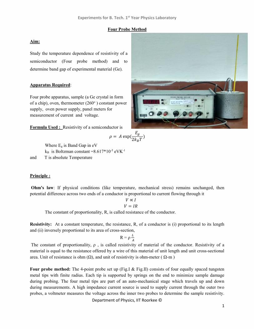
Apparatus Required: Four probe apparatus, sample (a Ge crystal in form of a chip), oven, thermometer (260o ) constant power supply, oven power supply, panel meters for measurement of current and voltage. Formula Used : Resistivity of a semiconductor is
𝜌 = 𝐴 exp (𝐸
2𝑘 𝑇 )
Where Eg is Band Gap in eV kB is Boltzman constant =8.617*10-5 eVK-1
and T is absolute Temperature Principle : Ohm's law: If physical conditions (like temperature, mechanical stress) remains unchanged, then potential difference across two ends of a conductor is proportional to current flowing through it
𝑉 ∝ 𝐼 𝑉 = 𝐼𝑅
The constant of proportionality, R, is called resistance of the conductor.
Resistivity: At a constant temperature, the resistance, R, of a conductor is (i) proportional to its length and (ii) inversely proportional to its area of cross-section,
R = ρ
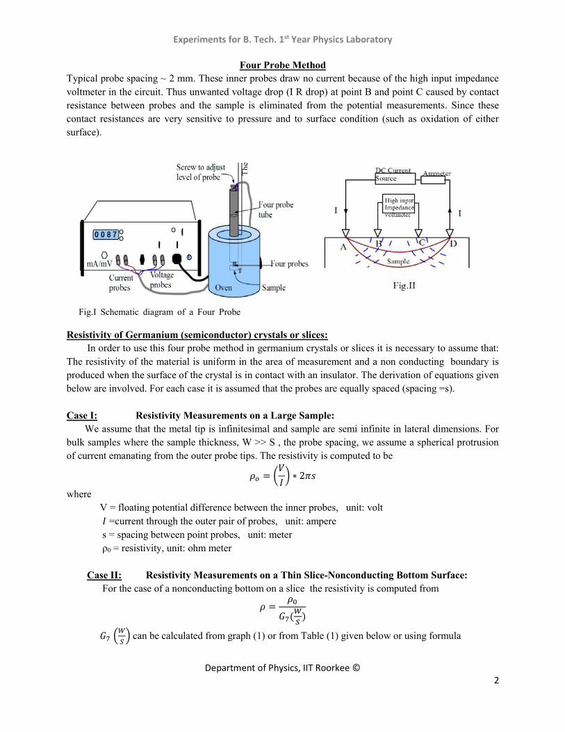
The constant of proportionality, ρ , is called resistivity of material of the conductor. Resistivity of a material is equal to the resistance offered by a wire of this material of unit length and unit cross-sectional area. Unit of resistance is ohm (Ω), and unit of resistivity is ohm-meter ( Ω-m ) Four probe method: The 4-point probe set up (Fig.I & Fig.II) consists of four equally spaced tungsten metal tips with finite radius. Each tip is supported by springs on the end to minimize sample damage during probing. The four metal tips are part of an auto-mechanical stage which travels up and down during measurements. A high impedance current source is used to supply current through the outer two probes, a voltmeter measures the voltage across the inner two probes to determine the sample resistivity.
Experiments for B. Tech. 1st Year Physics Laboratory
Four Probe Method
Department of Physics, IIT Roorkee © 2
Typical probe spacing ~ 2 mm. These inner probes draw no current because of the high input impedance voltmeter in the circuit. Thus unwanted voltage drop (I R drop) at point B and point C caused by contact resistance between probes and the sample is eliminated from the potential measurements. Since these contact resistances are very sensitive to pressure and to surface condition (such as oxidation of either surface).
Resistivity of Germanium (semiconductor) crystals or slices: In order to use this four probe method in germanium crystals or slices it is necessary to assume that:
The resistivity of the material is uniform in the area of measurement and a non conducting boundary is produced when the surface of the crystal is in contact with an insulator. The derivation of equations given below are involved. For each case it is assumed that the probes are equally spaced (spacing =s).
Case I: Resistivity Measurements on a Large Sample:
We assume that the metal tip is infinitesimal and sample are semi infinite in lateral dimensions. For bulk samples where the sample thickness, W >> S , the probe spacing, we assume a spherical protrusion of current emanating from the outer probe tips. The resistivity is computed to be
𝜌 =𝑉
𝐼∗ 2𝜋𝑠
where V = floating potential difference between the inner probes, unit: volt
𝐼 =current through the outer pair of probes, unit: ampere s = spacing between point probes, unit: meter ρ0 = resistivity, unit: ohm meter
Case II: Resistivity Measurements on a Thin Slice-Nonconducting Bottom Surface: For the case of a nonconducting bottom on a slice the resistivity is computed from
𝜌 =𝜌
𝐺 (𝑤𝑠
)
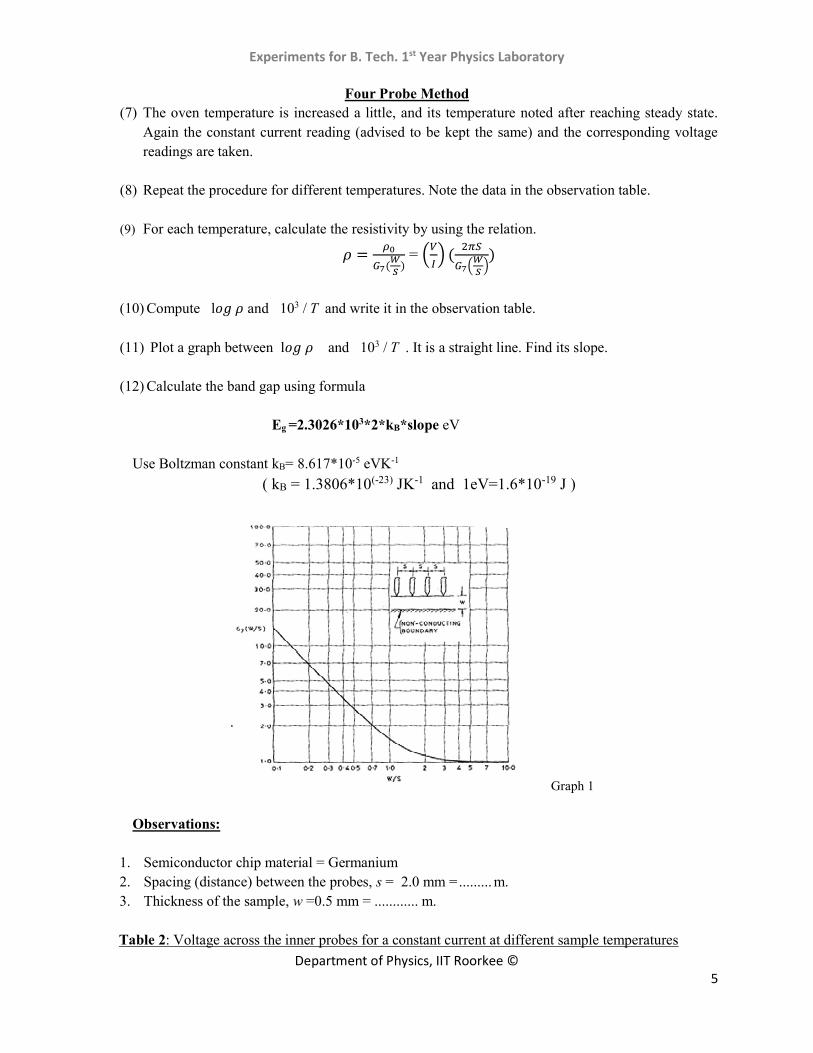
𝐺 can be calculated from graph (1) or from Table (1) given below or using formula
Fig.I Schematic diagram of a Four Probe
Experiments for B. Tech. 1st Year Physics Laboratory
Four Probe Method
Department of Physics, IIT Roorkee © 3
2log2
/7 ew
sswG
Table 1 S.No. W/S G7(W/S) S.No. W/S G7(W/S)
1. 0.100 13.863 6. 1.000 1.504 2. 0.141 9.704 7. 1.414 1.223 3. 0.200 9.631 8. 2.000 1.094 4. 0.330 4.159 9. 3.333 1.0228 5. 0.500 2.780 10. 5.000 1.0070
Temperature dependence of resistivity of a semiconductor:
Intrinsic semi-conduction The process in which thermally or optically excited electrons contribute to the conduction is called intrinsic semi-conduction. In the absence of photonic excitation, intrinsic semi-conduction takes place at temperatures above 0 K as sufficient thermal agitation is required to transfer electrons from the valence band to the conduction band. Conductivity for intrinsic semi-conduction. The total electrical conductivity is the sum of the conductivities of the valence and conduction band carriers, which are holes and electrons, respectively. It can be expressed as
σ = e(neμe + nhμh) (1)
where ne , μe are the electron's concentration and mobility, and nh , μh are the hole's concentration and mobility, respectively. Drift mobility determines the average drift velocity in the presence of an applied external field. It also depends on the temperature. The mobility is a quantity that directly relates the drift velocity vd of charge carriers to the applied electric field E across the material, i.e.,
μ = vd/ E …………. (2)
In the intrinsic region the number of electrons is equal to the number of holes, ne=nh=ni , so Equation (1) implies that,
σ = e𝑛 (μe + μh) (3)
The electron density (electrons/volume) in the conduction band is obtained by integrating (density of states x probability of occupancy of states) from the bottom to top of the conduction band. The detailed calculations reveal that
𝑛 = 𝑁𝑇 exp (− ) (4)
Where N is a contant substituting 𝑛 in eq (3)
σ =e (μe + μh) 𝑁𝑇 exp (− ) (5)
This shows that conductivity depends on temperature it decreases exponentially with decrease in temperature. Temperature dependence of resistivity
Experiments for B. Tech. 1st Year Physics Laboratory
Four Probe Method
Department of Physics, IIT Roorkee © 4
𝜌 = ( )
( ) (6)
Or,
𝜌 = 𝐴 exp ( ) (7)
Where A is a constant Taking Log
ln𝜌 = 𝑙𝑛𝐴 + (8)
or
log 𝜌 = 𝐶 +.
∗ (9)
where C is a constant . Rewriting eq (9)
log 𝜌 = 𝐶 +. ∗
∗ .
Therefore, if a graph is plotted log 𝜌 vs ( ) it should be a straight line and band gap Eg can be
determined from its slope as follows :
1. Slope =
=
. ∗∗ ,
2. Band gap Eg =2.3026*103*2*kB*slope eV, (Take Boltzman constant kB=8.617*10-5 eVK-1). Method : (1) The setting of 4-point probes on the semiconductor chip is a delicate process. So first understand
well the working of the apparatus. The semiconductor chip and probe set is costly. (2) Note the values of probe spacing (S) and the thickness (W) of the semiconductor chip. Note the
type of semiconductor (germanium or something else). (3) Make the circuit as shown in Fig.1. Put the sample in the oven (normally already placed by lab
instructor) at room temperature. (4) Pass a milliampere range current (say 5 mA) in the sample using constant current power supply. (5) The reading of the current through the sample is measured using milliammeter provided for this
purpose. The voltage is measured by a high impedance milli voltmeter connected to the inner probes. The readings can be taken alternately on digital meter provided for this purpose.
(6) Note temperature of sample (oven) using thermometer inserted in the oven for this purpose.
Experiments for B. Tech. 1st Year Physics Laboratory
Four Probe Method
Department of Physics, IIT Roorkee © 5
(7) The oven temperature is increased a little, and its temperature noted after reaching steady state. Again the constant current reading (advised to be kept the same) and the corresponding voltage readings are taken.
(8) Repeat the procedure for different temperatures. Note the data in the observation table.
(9) For each temperature, calculate the resistivity by using the relation.
𝜌 =( )
= ( )
(10) Compute l𝑜𝑔 𝜌 and 103 / T and write it in the observation table.
(11) Plot a graph between l𝑜𝑔 𝜌 and 103 / T . It is a straight line. Find its slope.
(12) Calculate the band gap using formula
Eg =2.3026*103*2*kB*slope eV
Use Boltzman constant kB= 8.617*10-5 eVK-1
( kB = 1.3806*10(-23) JK-1 and 1eV=1.6*10-19 J )
Graph 1
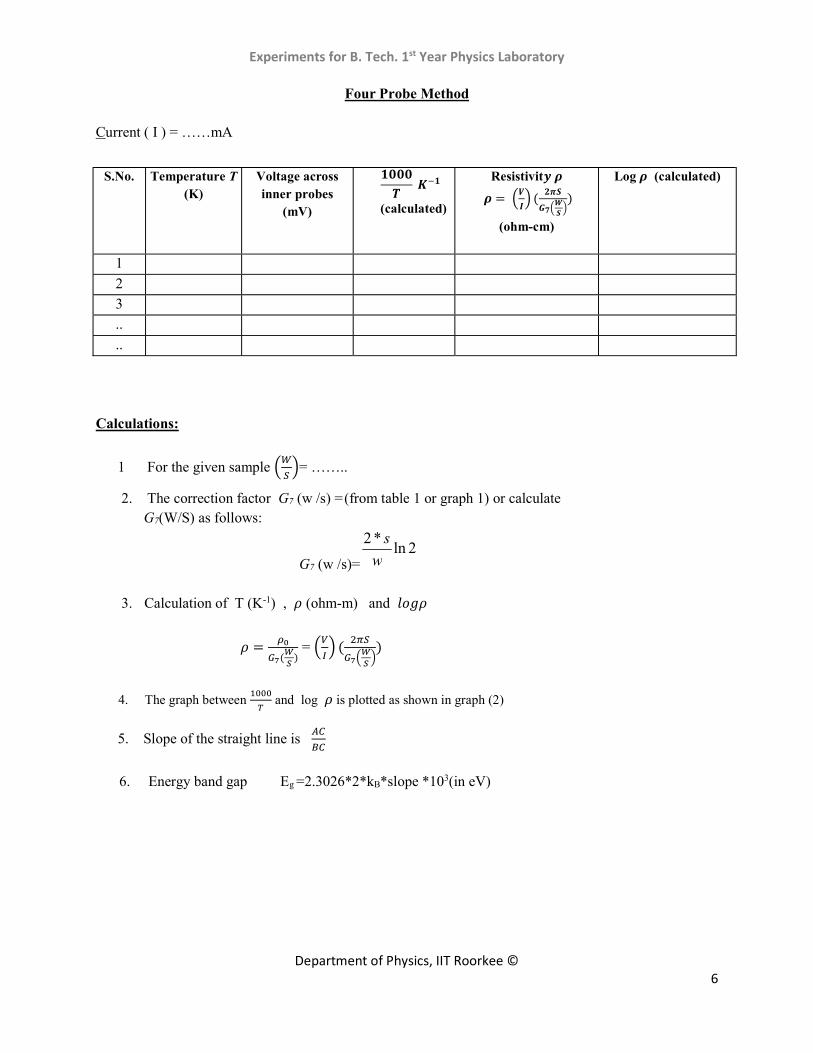
Observations:
1. Semiconductor chip material = Germanium 2. Spacing (distance) between the probes, s = 2.0 mm = ......... m. 3. Thickness of the sample, w =0.5 mm = ............ m. Table 2: Voltage across the inner probes for a constant current at different sample temperatures
Experiments for B. Tech. 1st Year Physics Laboratory
Four Probe Method
Department of Physics, IIT Roorkee © 6
Current ( I ) = ……mA
Calculations:
1 For the given sample = ……..
2. The correction factor G7 (w /s) =(from table 1 or graph 1) or calculate G7(W/S) as follows:
G7 (w /s)=2ln
*2
w
s
3. Calculation of T (K-1) , 𝜌 (ohm-m) and 𝑙𝑜𝑔𝜌
𝜌 =( )
= ( )
4. The graph between and log 𝜌 is plotted as shown in graph (2)
5. Slope of the straight line is
6. Energy band gap Eg =2.3026*2*kB*slope *103(in eV)
S.No. Temperature T (K)
Voltage across inner probes
(mV)
𝟏𝟎𝟎𝟎
𝑻 𝑲 𝟏
(calculated)
Resistivit𝒚 𝝆
𝝆 = 𝑽
𝑰(
𝟐𝝅𝑺
𝑮𝟕𝑾
𝑺
)
(ohm-cm)
Log 𝝆 (calculated)
1
2 3 ..
..
Experiments for B. Tech. 1st Year Physics Laboratory
Four Probe Method
Department of Physics, IIT Roorkee © 7
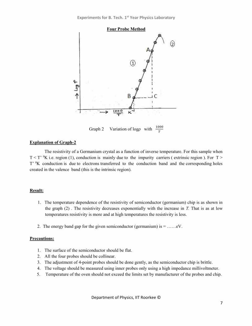
Graph 2 Variation of logρ with
Explanation of Graph-2
The resistivity of a Germanium crystal as a function of inverse temperature. For this sample when T < T’ 0K i.e. region (1), conduction is mainly due to the impurity carriers ( extrinsic region ). For T > T’ 0K conduction is due to electrons transferred to the conduction band and the corresponding holes created in the valence band (this is the intrinsic region).
Result:
1. The temperature dependence of the resistivity of semiconductor (germanium) chip is as shown in the graph (2) . The resistivity decreases exponentially with the increase in T. That is as at low temperatures resistivity is more and at high temperatures the resistivity is less.
2. The energy band gap for the given semiconductor (germanium) is = ……eV. Precautions:
1. The surface of the semiconductor should be flat. 2. All the four probes should be collinear. 3. The adjustment of 4-point probes should be done gently, as the semiconductor chip is brittle. 4. The voltage should be measured using inner probes only using a high impedance millivoltmeter. 5. Temperature of the oven should not exceed the limits set by manufacturer of the probes and chip.