s-24c32c/64c e2prom - ablic.com · the capacity of 32 k-bit and 64 k-bit, and the organization is...
TRANSCRIPT

S-24C32C/64C
www.ablicinc.com 2-WIRE SERIAL E2PROM
© ABLIC Inc., 2009-2013 Rev.4.0_03_H
1
The S-24C32C/64C is a 2-wire, low current consumption and wide range operation serial E2PROM. The S-24C32C/64C has the capacity of 32 K-bit and 64 K-bit, and the organization is 4096 words 8-bit, 8192 words 8-bit, respectively. Page write and sequential read are available.
Features
Operating voltage range Read: 1.6 V to 5.5 V Write: 1.7 V to 5.5 V Page write: 32 bytes / page Sequential read Operation frequency: 400 kHz (VCC = 1.6 V to 5.5 V) Write time: 5.0 ms max. Noise suppression: Schmitt trigger and noise filter on input pins (SCL, SDA) Write protect function during the low power supply voltage Endurance: 106cycles / word*1 (Ta = 25°C) Data retention: 100 years (Ta = 25°C) Memory capacity S-24C32C: 32 K-bit S-24C64C: 64 K-bit Write protect: 100% Initial shipment data: FFh Lead-free (Sn 100%), halogen-free*2
*1. For each address (Word: 8-bit) *2. Refer to “ Product Name Structure” for details.
Packages
8-Pin SOP (JEDEC) 8-Pin TSSOP TMSOP-8 SNT-8A
Caution This product is intended to use in general electronic devices such as consumer electronics, office equipment, and communication devices. Before using the product in medical equipment or automobile equipment including car audio, keyless entry and engine control unit, contact to ABLIC Inc. is indispensable.
www.ablic.com
2-WIRE SERIAL E2PROM S-24C32C/64C Rev.4.0_03_H
2
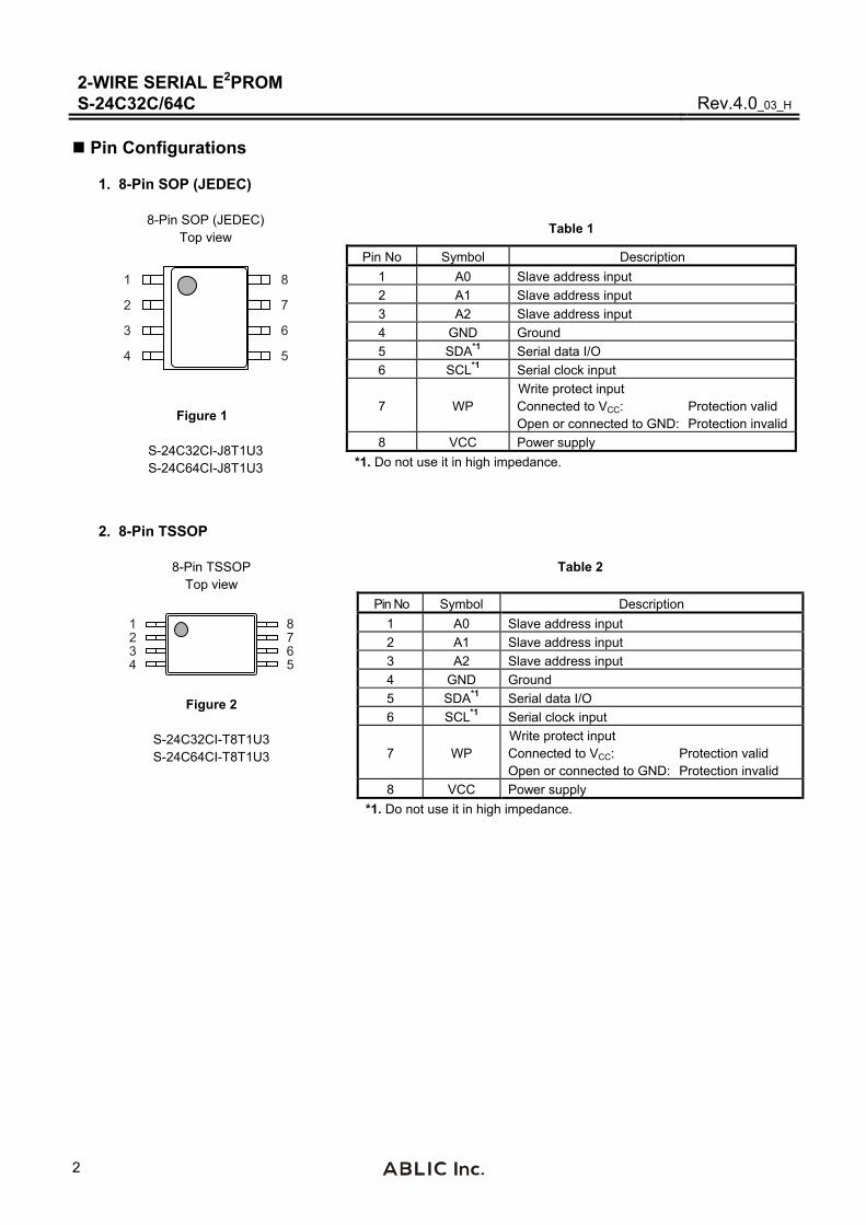
Pin Configurations
1. 8-Pin SOP (JEDEC)
8-Pin SOP (JEDEC) Top view
Table 1
7
6
5
8
2
3
4
1
Figure 1
S-24C32CI-J8T1U3 S-24C64CI-J8T1U3
Pin No Symbol Description
1 A0 Slave address input
2 A1 Slave address input
3 A2 Slave address input
4 GND Ground
5 SDA*1 Serial data I/O
6 SCL*1 Serial clock input
7 WP Write protect input Connected to VCC: Protection valid Open or connected to GND: Protection invalid
8 VCC Power supply
*1. Do not use it in high impedance.
2. 8-Pin TSSOP
8-Pin TSSOP Top view
Table 2
765
8234
1
Figure 2
S-24C32CI-T8T1U3 S-24C64CI-T8T1U3
Pin No Symbol Description
1 A0 Slave address input
2 A1 Slave address input
3 A2 Slave address input
4 GND Ground
5 SDA*1 Serial data I/O
6 SCL*1 Serial clock input
7 WP Write protect input Connected to VCC: Protection valid Open or connected to GND: Protection invalid
8 VCC Power supply
*1. Do not use it in high impedance.

2-WIRE SERIAL E2PROMRev.4.0_03_H S-24C32C/64C
3
3. TMSOP-8
TMSOP-8 Top view
Table 3
765
8234
1
Figure 3
S-24C32CI-K8T3U3 S-24C64CI-K8T3U3
Pin No Symbol Description
1 A0 Slave address input
2 A1 Slave address input
3 A2 Slave address input
4 GND Ground
5 SDA*1 Serial data I/O
6 SCL*1 Serial clock input
7 WP Write protect input Connected to VCC: Protection valid Open or connected to GND: Protection invalid
8 VCC Power supply
*1. Do not use it in high impedance.
4. SNT-8A
SNT-8A Top view
Table 4
765
8234
1
Figure 4
S-24C32CI-I8T1U3
Pin No Symbol Description
1 A0 Slave address input
2 A1 Slave address input
3 A2 Slave address input
4 GND Ground
5 SDA*1 Serial data I/O
6 SCL*1 Serial clock input
7 WP Write protect input Connected to VCC: Protection valid Open or connected to GND: Protection invalid
8 VCC Power supply
*1. Do not use it in high impedance.
Remark Refer to the “Package drawings” for the details.

2-WIRE SERIAL E2PROM S-24C32C/64C Rev.4.0_03_H
4
Block Diagram
VCC
GND SCL
SDA
DIN
DOUT
R / W
LOAD INC
COMP
LOAD
WP
Start / Stop Detector
Serial Clock Controller High-Voltage Generator
Voltage Detector
Device Address Comparator
Address Counter
Y Decoder
Data Register
Memory Cell ArrayX Decoder
Selector
Data Output ACK Output Controller
A2
A1
A0
Figure 5

2-WIRE SERIAL E2PROMRev.4.0_03_H S-24C32C/64C
5
Absolute Maximum Ratings
Table 5
Item Symbol Absolute Maximum Ratings Unit
Power supply voltage VCC 0.3 to 6.5 V
Input voltage VIN 0.3 to 6.5 V
Output voltage VOUT 0.3 to 6.5 V
Operation ambient temperature Topr 40 to 85 °C
Storage temperature Tstg 65 to 150 °C
Caution The absolute maximum ratings are rated values exceeding which the product could suffer physical damage. These values must therefore not be exceeded under any conditions.
Recommended Operating Conditions
Table 6
Item Symbol Condition Ta = 40°C to 85°C
Unit Min. Max.
Power supply voltage VCC Read Operation 1.6 5.5 V Write Operation 1.7 5.5 V
High level input voltage VIH VCC = 1.6 V to 5.5 V 0.7 VCC 5.5 V Low level input voltage VIL VCC = 1.6 V to 5.5 V 0.3 0.3 VCC V
Pin Capacitance
Table 7 (Ta = 25°C, f = 1.0 MHz, VCC = 5.0 V)
Item Symbol Condition Min. Max. Unit
Input capacitance CIN VIN = 0 V (SCL, A0, A1, A2, WP) 10 pF
I/O capacitance CI / O VI / O = 0 V (SDA) 10 pF
Endurance
Table 8
Item Symbol Operation Ambient Temperature Min. Max. Unit
Endurance NW Ta = 25°C 106 cycles / word*1
*1. For each address (Word: 8-bit)
Data Retention
Table 9
Item Symbol Operation Ambient Temperature Min. Max. Unit
Data retention Ta = 25°C 100 year
2-WIRE SERIAL E2PROM S-24C32C/64C Rev.4.0_03_H
6
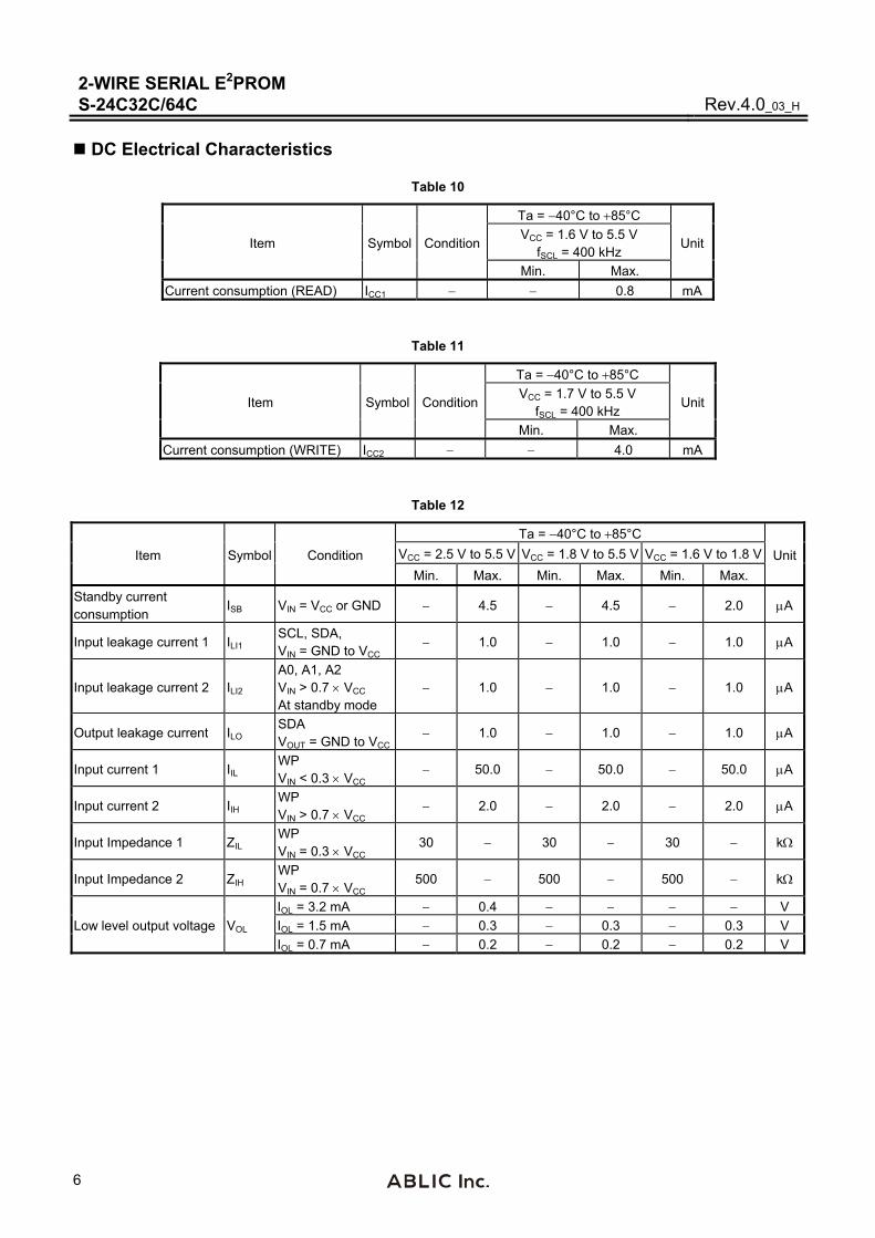
DC Electrical Characteristics
Table 10
Item Symbol Condition
Ta = 40°C to 85°C
Unit VCC = 1.6 V to 5.5 V
fSCL = 400 kHz
Min. Max.
Current consumption (READ) ICC1 0.8 mA
Table 11
Item Symbol Condition
Ta = 40°C to 85°C
Unit VCC = 1.7 V to 5.5 V
fSCL = 400 kHz
Min. Max.
Current consumption (WRITE) ICC2 4.0 mA
Table 12
Item Symbol Condition
Ta = 40°C to 85°C
UnitVCC = 2.5 V to 5.5 V VCC = 1.8 V to 5.5 V VCC = 1.6 V to 1.8 V
Min. Max. Min. Max. Min. Max.
Standby current consumption
ISB VIN = VCC or GND 4.5 4.5 2.0 A
Input leakage current 1 ILI1 SCL, SDA, VIN = GND to VCC
1.0 1.0 1.0 A
Input leakage current 2 ILI2 A0, A1, A2 VIN > 0.7 VCC
At standby mode 1.0 1.0 1.0 A
Output leakage current ILO SDA VOUT = GND to VCC
1.0 1.0 1.0 A
Input current 1 IIL WP VIN < 0.3 VCC
50.0 50.0 50.0 A
Input current 2 IIH WP VIN > 0.7 VCC
2.0 2.0 2.0 A
Input Impedance 1 ZIL WP VIN = 0.3 VCC
30 30 30 k
Input Impedance 2 ZIH WP VIN = 0.7 VCC
500 500 500 k
Low level output voltage VOL
IOL = 3.2 mA 0.4 V
IOL = 1.5 mA 0.3 0.3 0.3 V
IOL = 0.7 mA 0.2 0.2 0.2 V

2-WIRE SERIAL E2PROMRev.4.0_03_H S-24C32C/64C
7
AC Electrical Characteristics
Table 13 Measurement Conditions
0.8 VCC
Input pulse voltage Output reference voltage
0.2 VCC
0.7 VCC
0.3 VCC
Input pulse voltage 0.2 VCC to 0.8 VCC
Input pulse rising / falling time 20 ns or less
Output reference voltage 0.3 VCC to 0.7 VCC
Output load 100 pF
Figure 6 I/O Waveform during AC Measurement
Table 14
Item Symbol
Ta = 40°C to 85°C
Unit VCC = 1.6 V to 5.5 V
Min. Max.
SCL clock frequency fSCL 0 400 kHz
SCL clock time “L” tLOW 1.3 s
SCL clock time “H” tHIGH 0.6 s
SDA output delay time tAA 0.1 0.9 s
SDA output hold time tDH 50 ns
Start condition setup time tSU.STA 0.6 s
Start condition hold time tHD.STA 0.6 s
Data input setup time tSU.DAT 100 ns
Data input hold time tHD.DAT 0 ns
Stop condition setup time tSU.STO 0.6 s
SCL, SDA rising time tR 0.3 s
SCL, SDA falling time tF 0.3 s
WP setup time tWS1 0 s
WP hold time tWH1 0 s
WP release setup time tWS2 0 s
WP release hold time tWH2 0 s
Bus release time tBUF 1.3 s
Noise suppression time tI 50 ns
SCL
SDA ( input )
SDA ( output )
tBUF
tR
tSU.STO
tSU.DAT tHD.DAT
tDH tAA
tHIGH tLOW
tHD.STA
tSU.STA
tF
Figure 7 Bus Timing

2-WIRE SERIAL E2PROM S-24C32C/64C Rev.4.0_03_H
8
Table 15
Item Symbol
Ta = 40°C to 85°C
Unit VCC = 1.7 V to 5.5 V
Min. Max.
Write time tWR 5.0 ms
SCL
SDA D0
Write dataAcknowledgment
Signal Stop Condition Start ConditiontWR Start Condition
WP (valid)
WP (invalid)
tWS1 tWH1
tWS2 tWH2
Figure 8 Write Cycle Timing
2-WIRE SERIAL E2PROMRev.4.0_03_H S-24C32C/64C
9
Pin Functions
1. A0, A1 and A2 (Slave Address Input) Pins
In the S-24C32C/64C, to set the slave address, connect each pin of A0, A1, A2 to GND or VCC. Therefore the users can set 8 types of slave address by a combination of A0, A1, A2 pins.
Comparing the slave address transmitted from the master device and one that you set, makes possible to select the S-24C32C/64C from other devices connected onto the bus. Each A0, A1 and A2 pin has a pull-down resistor. In open, these pins have the status when they are connected to GND.
2. SDA (Serial Data Input / Output) Pin
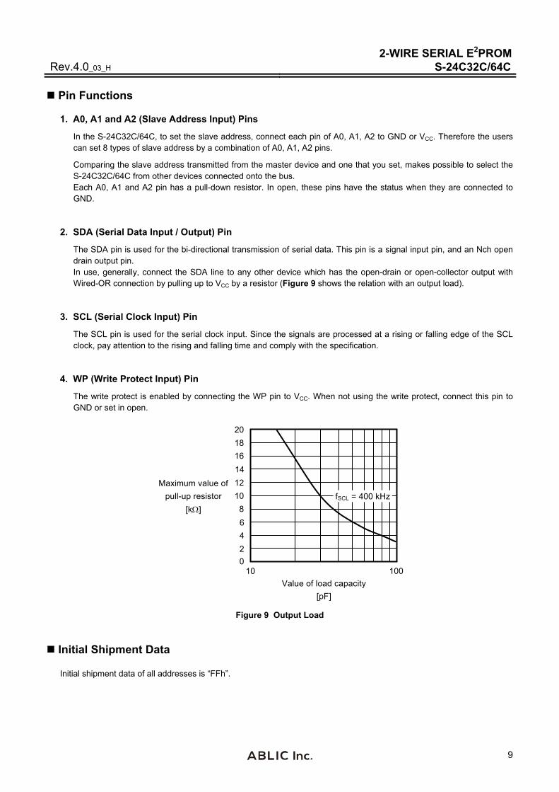
The SDA pin is used for the bi-directional transmission of serial data. This pin is a signal input pin, and an Nch open drain output pin. In use, generally, connect the SDA line to any other device which has the open-drain or open-collector output with Wired-OR connection by pulling up to VCC by a resistor (Figure 9 shows the relation with an output load).
3. SCL (Serial Clock Input) Pin
The SCL pin is used for the serial clock input. Since the signals are processed at a rising or falling edge of the SCL clock, pay attention to the rising and falling time and comply with the specification.
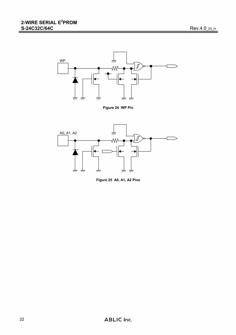
4. WP (Write Protect Input) Pin
The write protect is enabled by connecting the WP pin to VCC. When not using the write protect, connect this pin to GND or set in open.
Value of load capacity
[pF]
100 100
2
4
6
8
fSCL = 400 kHz
Maximum value of
pull-up resistor
[k]
10
12
14
16
18
20
Figure 9 Output Load
Initial Shipment Data Initial shipment data of all addresses is “FFh”.

2-WIRE SERIAL E2PROM S-24C32C/64C Rev.4.0_03_H
10
Operation 1. Start Condition
Start is identified by a high to low transition of the SDA line while the SCL line is stable at high. Every operation begins from a start condition.
2. Stop Condition
Stop is identified by a low to high transition of the SDA line while the SCL line is stable at high. When a device receives a stop condition during a read sequence, the read operation is interrupted, and the device enters standby mode. When a device receives a stop condition during a write sequence, the reception of the write data is halted, and the S-24C32C/64C initiates a write cycle.
tSU.STA tHD.STA tSU.STO
Start Condition Stop Condition
SCL
SDA
Figure 10 Start / Stop Conditions

2-WIRE SERIAL E2PROMRev.4.0_03_H S-24C32C/64C
11
3. Data Transmission
Changing the SDA line while the SCL line is low, data is transmitted. Changing the SDA line while the SCL line is high, a start or stop condition is recognized.
tSU.DAT tHD.DAT
SCL
SDA
Figure 11 Data Transmission Timing
4. Acknowledge
The unit of data transmission is 8 bits. During the 9th clock cycle period the receiver on the bus pulls down the SDA line to acknowledge the receipt of the 8-bit data. When an internal write cycle is in progress, the device does not generate an acknowledge.
1 8 9
Acknowledge Output
tAA tDH
Start Condition
SCL (E2PROM Input)
SDA (Master Output)
SDA (E2PROM Output)
Figure 12 Acknowledge Output Timing

2-WIRE SERIAL E2PROM S-24C32C/64C Rev.4.0_03_H
12
5. Device Addressing
To start communication, the master device on the system generates a start condition to the bus line. Next, the master device sends 7-bit device address and a 1-bit read / write instruction code on to the SDA bus. The upper 4 bits of the device address are the “Device Code”, and are fixed to “1010”. In the S-24C32C/64C, successive 3 bits are the “Slave Address”. These 3 bits are used to identify a device on the system bus and is compared with the predetermined value which is defined by the address input pins (A2, A1, A0). When the comparison result matches, the slave device responds with an acknowlede during the 9th clocks cycle.
Slave AddressDevice Code
MSB LSB
1 0 1 0 A2 A1 A0 R / W
Figure 13 Device Address

2-WIRE SERIAL E2PROMRev.4.0_03_H S-24C32C/64C
13
6. Write
6. 1 Byte write
When the master sends a 7-bit device address and a 1-bit read / write instruction code set to “0”, following a start condition, the S-24C32C/64C acknowledges it. The S-24C32C/64C then receives a upper 8-bit word address and responds with an acknowledge. And the S-24C32C/64C receives a lower 8-bit word address and responds with an acknowledge. After the S-24C32C/64C receives 8-bit write data and responds with an acknowledge, it receives a stop condition and that initiates the write cycle at the addressed memory. During the write cycle all operations are forbidden and no acknowledge is generated.
A2 A1 A0
S T A R T
1 0 1 0
W R I T E
DEVICE ADDRESS
UPPER WORD ADDRESS
R /
W
M S B
SDA LINE
A C K
L S B
LOWER WORD ADDRESS
0
STOPDATA
X W7 W6 W5 W4 W3 W2 W1 W0 D7 D6 D5 D4 D3 D2 D1 D0W12 W11 W10 W9 W8
ACK
ACK
X
A C K
X
Remark In the S-24C32C, W12 = Don’t care.
Figure 14 Byte Write
2-WIRE SERIAL E2PROM S-24C32C/64C Rev.4.0_03_H
14
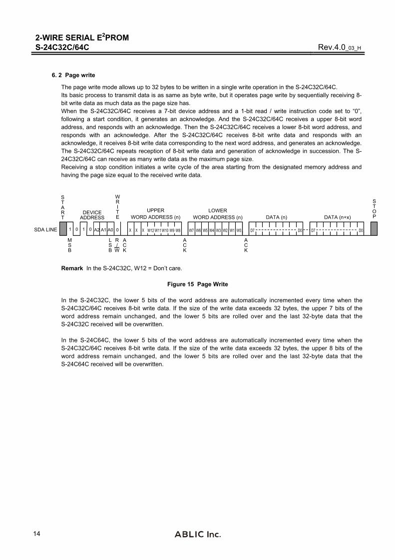
6. 2 Page write
The page write mode allows up to 32 bytes to be written in a single write operation in the S-24C32C/64C. Its basic process to transmit data is as same as byte write, but it operates page write by sequentially receiving 8-bit write data as much data as the page size has. When the S-24C32C/64C receives a 7-bit device address and a 1-bit read / write instruction code set to “0”, following a start condition, it generates an acknowledge. And the S-24C32C/64C receives a upper 8-bit word address, and responds with an acknowledge. Then the S-24C32C/64C receives a lower 8-bit word address, and responds with an acknowledge. After the S-24C32C/64C receives 8-bit write data and responds with an acknowledge, it receives 8-bit write data corresponding to the next word address, and generates an acknowledge. The S-24C32C/64C repeats reception of 8-bit write data and generation of acknowledge in succession. The S-24C32C/64C can receive as many write data as the maximum page size. Receiving a stop condition initiates a write cycle of the area starting from the designated memory address and having the page size equal to the received write data.
A2 A1 A0
S T A R T
1 0 1 0
WR I T E
DEVICE ADDRESS
UPPER WORD ADDRESS (n)
R/
W
M S B
SDA LINE
A C K
L S B
LOWER WORD ADDRESS (n)
0 X W7 W6 W5 W4 W3 W2 W1 W0
DATA (n)
D7 D0
STOP
W12 W11 W10 W9 W8
ACK
X
ACK
DATA (n+x)
D7 D0X
Remark In the S-24C32C, W12 = Don’t care.
Figure 15 Page Write
In the S-24C32C, the lower 5 bits of the word address are automatically incremented every time when the S-24C32C/64C receives 8-bit write data. If the size of the write data exceeds 32 bytes, the upper 7 bits of the word address remain unchanged, and the lower 5 bits are rolled over and the last 32-byte data that the S-24C32C received will be overwritten. In the S-24C64C, the lower 5 bits of the word address are automatically incremented every time when the S-24C32C/64C receives 8-bit write data. If the size of the write data exceeds 32 bytes, the upper 8 bits of the word address remain unchanged, and the lower 5 bits are rolled over and the last 32-byte data that the S-24C64C received will be overwritten.

2-WIRE SERIAL E2PROMRev.4.0_03_H S-24C32C/64C
15
6. 3 Write protect
Write protect is available in the S-24C32C/64C. When the WP pin is connected to the VCC, write operation to memory area is inhibited. When the WP pin is connected to GND or set in open, the write protect is invalid, and write operation in all memory area is available. Fix the level of the WP pin from start condition in the write operation (byte write, page write) until stop condition. If the WP pin changes during this time, the address data being written at this time is not guaranteed. Regarding the timing of write protect, refer to Figure 8. In not using the write protect, connect the WP pin to GND or set it open. The write protect is valid in the range of operation power supply voltage. As seen in Figure 16 when the write protect is valid, the S-24C32C/64C does not generate an acknowledgment signal after data input.
A2 A1 A0
S T A R T
1 0 1 0
W R I T E
DEVICE ADDRESS
UPPER WORD ADDRESS
R /
W
M S B
SDA LINE
A C K
LSB
LOWER WORD ADDRESS
0
STOPDATA
X W7 W6 W5 W4 W3 W2 W1 W0 D7 D6 D5 D4 D3 D2 D1 D0W12 W11 W10 W9 W8
ACK
NACK
X
ACK
WP
X
Remark In the S-24C32C, W12 = Don’t care.
Figure 16 Write Protect
2-WIRE SERIAL E2PROM S-24C32C/64C Rev.4.0_03_H
16
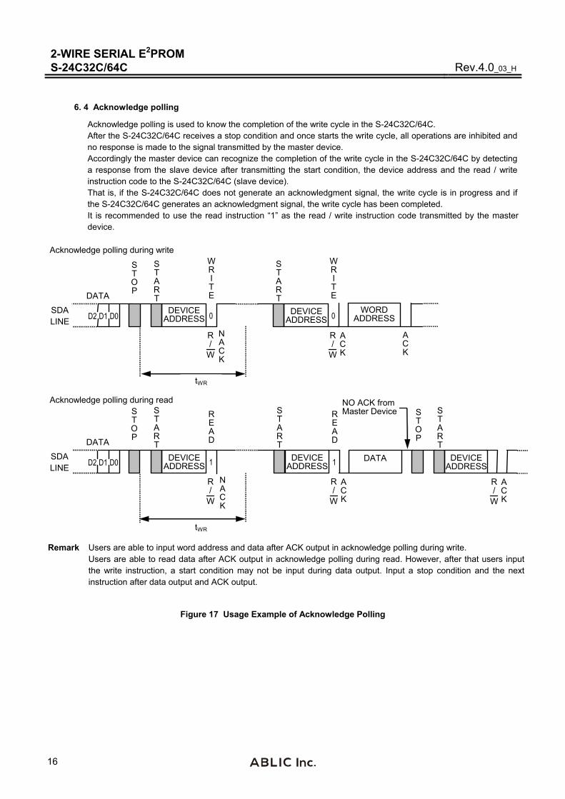
6. 4 Acknowledge polling
Acknowledge polling is used to know the completion of the write cycle in the S-24C32C/64C. After the S-24C32C/64C receives a stop condition and once starts the write cycle, all operations are inhibited and no response is made to the signal transmitted by the master device. Accordingly the master device can recognize the completion of the write cycle in the S-24C32C/64C by detecting a response from the slave device after transmitting the start condition, the device address and the read / write instruction code to the S-24C32C/64C (slave device). That is, if the S-24C32C/64C does not generate an acknowledgment signal, the write cycle is in progress and if the S-24C32C/64C generates an acknowledgment signal, the write cycle has been completed. It is recommended to use the read instruction “1” as the read / write instruction code transmitted by the master device.
S T A R T
ACK
N A C K
Remark Users are able to input word address and data after ACK output in acknowledge polling during write. Users are able to read data after ACK output in acknowledge polling during read. However, after that users input the write instruction, a start condition may not be input during data output. Input a stop condition and the next instruction after data output and ACK output.
SDA LINE
DEVICE ADDRESS
DATA
D2 D1 D0
S T O P
tWR
ST A R T
S T A R T
ACK
SDA LINE
DATA
D2 D1 D0
S T O P
tWR
ST A R T
N A C K
S T O P
DATA
NO ACK fromMaster Device R
E A D
R /
W
1
W R I T E
R /
W
0 DEVICE
ADDRESS
WRI TE
R/
W
0DEVICEADDRESS
DEVICEADDRESS
RE A D
R/
W
1
Acknowledge polling during write
Acknowledge polling during read
ACK
S T A R T
DEVICEADDRESS
R/
W
A C K
WORDADDRESS
Figure 17 Usage Example of Acknowledge Polling

2-WIRE SERIAL E2PROMRev.4.0_03_H S-24C32C/64C
17
7. Read
7. 1 Current address read
Either in writing or in reading the S-24C32C/64C holds the last accessed memory address. The memory address is maintained as long as the power voltage does not decrease less than the operating voltage. The master device can read the data at the memory address of the current address pointer without assigning the word address as a result, when it recognizes the position of the address pointer in the S-24C32C/64C. This is called “Current Address Read”. In the following the address counter in the S-24C32C/64C is assumed to be “n”. When the S-24C32C/64C receives a 7-bit device address and a 1-bit read / write instruction code set to “1” following a start condition, it responds with an acknowledge. Next, an 8-bit data at the address “n” is sent from the S-24C32C/64C synchronous to the SCL clock. The address counter is incremented and the content of the address counter becomes n1. The master device outputs stop condition not an acknowledge, the reading of S-24C32C/64C is ended.
S T A R T
1 0 1 0
READ
S T O P
DEVICE ADDRESS
R /
W
M S B
SDA LINE A2 A1 A0 D7 D6 D5 D4 D3 D2 D1D0
A C K
L S B
1
DATA
NO ACK from Master Device
Figure 18 Current Address Read
Attention should be paid to the following point on the recognition of the address pointer in the S-24C32C/64C. In Read, the memory address counter in the S-24C32C/64C is automatically incremented after output of the 8th bit of the data. In Write, on the other hand, the upper bits of the memory address (the upper bits of the word address*1) are left unchanged and are not incremented. *1. In the S-24C32C, the upper 7 bits of the word address. In the S-24C64C, the upper 8 bits of the word address.

2-WIRE SERIAL E2PROM S-24C32C/64C Rev.4.0_03_H
18
7. 2 Random read
Random read is used to read the data at an arbitrary memory address. A dummy write is performed to load the memory address into the address counter. When the S-24C32C/64C receives a 7-bit device address and a 1-bit read / write instruction code set to “0” following a start condition, it responds with an acknowledge. The S-24C32C/64C then receives a upper 8-bit word address and responds with an acknowledge. And the S-24C32C/64C receives a lower 8-bit word address and responds with an acknowledge. The memory address is loaded to the address counter in the S-24C32C/64C by these operations. Reception of write data does not follow in a dummy write whereas reception of write data follows in byte write and in page write. Since the memory address is loaded into the memory address counter by dummy write, the master device can read the data starting from the arbitrary memory address by transmitting a new start condition and performing the same operation in the current address read. That is, when the S-24C32C/64C receives a 7-bit device address and a 1-bit read / write instruction code set to “1”, following a start condition signal, it responds with an acknowledge. Next, 8-bit data is transmitted from the S-24C32C/64C in synchronous to the SCL clock. The master device outputs stop condition not an acknowledge, the reading of S-24C32C/64C is ended.
SDA LINE
S T A R T
1 0 1 0
W R I T E
DEVICE ADDRESS
LOWER WORD ADDRESS
R /
W
M S B
A2 A1 A0
A C K
L S B
W7 W6 W5 W4 W3 W2 W1
ACK
0
DUMMY WRITE
STO P
ST A R T
1 0 1 0
R E A D
DEVICE ADDRESS
R /
W
MSB
A2 A1 A0
A C K
L S B
1 下図へ続く
NO ACK fromMaster Device
DATA UPPER
WORD ADDRESS
X W9W8X D7 D6 D5 D4 D3 D2 D1 D0
ACK
W11 W10 W0X X W12
Remark In the S-24C32C, W12 = Don’t care.
Figure 19 Random Read

2-WIRE SERIAL E2PROMRev.4.0_03_H S-24C32C/64C
19
7. 3 Sequential read
When the S-24C32C/64C receives a 7-bit device address and a 1-bit read / write instruction code set to “1” following a start condition both in current address read and random read, it responds with an acknowledge. When an 8-bit data is output from the S-24C32C/64C synchronous to the SCL clock, the address counter is automatically incremented. When the master device responds with an acknowledge, the data at the next memory address is transmitted. Response with an acknowledge by the master device has the memory address counter in the S-24C32C/64C incremented and makes it possible to read data in succession. This is called “Sequential Read”. The master device outputs stop condition not an acknowledge, the reading of S-24C32C/64C is ended. Data can be read in succession in the sequential read mode. When the memory address counter reaches the last word address, it rolls over to the first word address.
R E A D
STOP
DEVICE ADDRESS
R /
W
A C K
ACK
ACK
1
A C K
SDA LINE
DATA (n)
D7 D0 D7 D0D7 D0 D7 D0
DATA (n+1) DATA (n+2) DATA (n+x)
NO ACK fromMaster Device
Figure 20 Sequential Read

2-WIRE SERIAL E2PROM S-24C32C/64C Rev.4.0_03_H
20
Write Protect Function during the Low Power Supply Voltage
The S-24C32C/64C has a built-in detection circuit which operates with the low power supply voltage, cancels Write when the power supply voltage drops and power-on. Its detection and release voltages are 1.20 V typ. (Refer to Figure 21). The S-24C32C/64C cancels Write by detecting a low power supply voltage when it receives a stop condition. In the data trasmission and the Write operation, data in the address written during the low power supply voltage is not assurable.
Release Voltage (VDET) 1.20 V typ.
Power Supply Voltage
Detection Voltage (VDET)1.20 V typ.
Write Instruction cancel
Figure 21 Operation during Low Power Supply Voltage

2-WIRE SERIAL E2PROMRev.4.0_03_H S-24C32C/64C
21
Using S-24C32C/64C
1. Adding a pull-up resistor to SDA I/O pin and SCL input pin
In consideration of I2C-bus protocol function, the SDA I/O pins should be connected with a pull-up resistor. The S-24C32C/64C cannot transmit normally without using a pull-up resistor.
In case that the SCL input pin of the S-24C32C/64C is connected to the Nch open drain output pin of the master device, connect the SCL pin with a pull-up resistor. As well, in case the SCL input pin of the S-24C32C/64C is connected to the tri-state output pin of the master device, connect the SCL pin with a pull-up resistor in order not to set it in high impedance. This prevents the S-24C32C/64C from error caused by an uncertain output (high impedance) from the tri-state pin when resetting the master device during the voltage drop.
2. Equivalent circuit of input and I/O pin
The S-24C32C/64C does not have a built-in pull-down or pull-up resistor for the SCL and SDA pins. The WP, A2, A1 and A0 pins have a pull-down resistor. The SDA pin has an open-drain output. The followings are equivalent circuits of the pins.
SCL
Figure 22 SCL Pin
SDA
Figure 23 SDA Pin
2-WIRE SERIAL E2PROM S-24C32C/64C Rev.4.0_03_H
22
WP
Figure 24 WP Pin
A0, A1, A2
Figure 25 A0, A1, A2 Pins

2-WIRE SERIAL E2PROMRev.4.0_03_H S-24C32C/64C
23
3. Phase adjustment during S-24C32C/64C access
The S-24C32C/64C does not have a pin to reset (the internal circuit). The users cannot forcibly reset it externally. If the communication to the S-24C32C/64C interrupted, the users need to handle it as you do for software. In the S-24C32C/64C, users are able to reset the internal circuit by inputting a start condition and a stop condition. Although the reset signal is input to the master device, the S-24C32C/64C’s internal circuit does not go in reset, but it does by inputting a stop condition to the S-24C32C/64C. The S-24C32C/64C keeps the same status thus cannot do the next operation. Especially, this case corresponds to that only the master device is reset when the power supply voltage drops. If the power supply voltage restored in this status, input the instruction after resetting (adjusting the phase with the master device) the S-24C32C/64C. How to reset is shown below.
[How to reset S-24C32C/64C]
The S-24C32C/64C is able to be reset by a start and stop instructions. When the S-24C32C/64C is reading data “0” or is outputting the acknowledgment signal, outputs “0” to the SDA line. In this status, the master device cannot output an instruction to the SDA line. In this case, terminate the acknowledgment output operation or the Read operation, and then input a start instruction. Figure 26 shows this procedure. First, input a start condition. Then transmit 9 clocks (dummy clock) of SCL. During this time, the master device sets the SDA line to “H”. By this operation, the S-24C32C/64C interrupts the acknowledgment output operation or data output, so input a start condition*1. When a start condition is input, the S-24C32C/64C is reset. To make doubly sure, input the stop condition to the S-24C32C/64C. The normal operation is then possible.
1 2 8 9
SCL
SDA
Start Condition
Stop Condition
Start ConditionDummy Clock
Figure 26 Resetting S-24C32C/64C *1. After 9 clocks (dummy clock), if the SCL clock continues to being output without inputting a start condition,
S-24C32C/64C may go in the write operation when it receives a stop condition. To prevent this, input a start condition after 9 clocks (dummy clock).
Remark Regarding this reset procedure with dummy clock, it is recommended to perform at the system
initialization after applying the power supply voltage.

2-WIRE SERIAL E2PROM S-24C32C/64C Rev.4.0_03_H
24
4. Acknowledge check
The I2C-bus protocol includes an acknowledge check function as a handshake function to prevent a communication error. This function allows detection of a communication failure during data communication between the master device and S-24C32C/64C. This function is effective to prevent malfunction, so it is recommended to perform an acknowledge check with the master device.
5. Built-in power-on-clear circuit
The S-24C32C/64C has a built-in power-on-clear circuit that initializes itself at the same time during power-on. Unsuccessful initialization may cause a malfunction. To operate the power-on-clear circuit normally, the following conditions must be satisfied to raise the power supply voltage.
5. 1 Raising power supply voltage
Shown in Figure 27, raise the power supply voltage from 0.2 V max., within the time defined as tRISE which is the time required to reach the power supply voltage to be set. For example, if the power supply voltage is 5.0 V, tRISE = 200 ms seen in Figure 28. The power supply voltage must be raised within 200 ms.
0.2 V VINIT max.
tINIT*2 max.
tRISE max.
Power Supply Voltage (VCC)
0 V*1
*1. 0 V means there is no difference in potential between the VCC pin and the GND pin of the S-24C32C/64C. *2. tINIT is the time required to initialize the S-24C32C/64C. No instructions are accepted during this time.
Figure 27 Raising Power Supply Voltage

2-WIRE SERIAL E2PROMRev.4.0_03_H S-24C32C/64C
25
Power Supply Voltage Rise Time (tRISE) max. [ms]
Power Supply Voltage (VCC)
[V]
50
5.0
4.0
3.0
2.0
100 150 200
For example: If the power supply voltage = 5.0 V, raise the voltage to 5.0 V within 200 ms.
Figure 28 Power Supply Voltage Rise Time
When initialization is successfully completed by the power-on-clear circuit, the S-24C32C/64C enters the standby status. If the power-on-clear circuit does not operate; The S-24C32C/64C has not completed initialization, an instruction previously input is still valid or an instruction may be inappropriately recognized. In this case, S-24C32C/64C may perform the Write operation. The voltage drops due to power off while the S-24C32C/64C is being accessed. Even if the master device is reset due to the low power voltage, the S-24C32C/64C may malfunction unless the power-on-clear operation conditions of S-24C32C/64C are satisfied.
When not keeping to the power supply voltage rise time seen in Figure 28, adjust the phase (reset) to reset the internal circuit in the S-24C32C/64C normally.

2-WIRE SERIAL E2PROM S-24C32C/64C Rev.4.0_03_H
26
5. 2 Initialization time
The S-24C32C/64C initializes at the same time when the power supply voltage is raised. Input instructions to the S-24C32C/64C after initialization. S-24C32C/64C does not accept any instruction during initialization. Figure 29 shows the initialization time of the S-24C32C/64C.
Power Supply Voltage Rise Time (tRISE) [s]
Initialization Time
(tINIT) max. [s]
100 m
10 m
1.0 m
100
10
1.0
1.0 10 100 1.0 m 10 m 100 m
Figure 29 Initialization Time of S-24C32C/64C
2-WIRE SERIAL E2PROMRev.4.0_03_H S-24C32C/64C
27
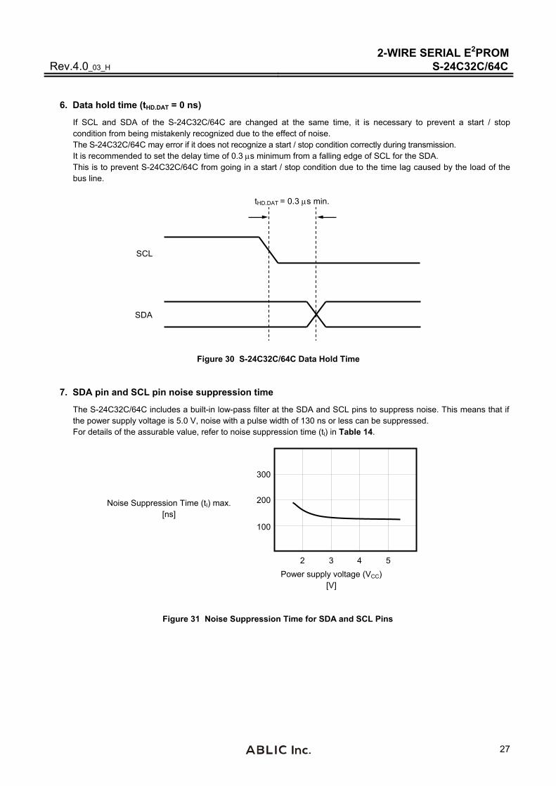
6. Data hold time (tHD.DAT = 0 ns)
If SCL and SDA of the S-24C32C/64C are changed at the same time, it is necessary to prevent a start / stop condition from being mistakenly recognized due to the effect of noise. The S-24C32C/64C may error if it does not recognize a start / stop condition correctly during transmission. It is recommended to set the delay time of 0.3 s minimum from a falling edge of SCL for the SDA. This is to prevent S-24C32C/64C from going in a start / stop condition due to the time lag caused by the load of the bus line.
SCL
SDA
tHD.DAT = 0.3 s min.
Figure 30 S-24C32C/64C Data Hold Time
7. SDA pin and SCL pin noise suppression time
The S-24C32C/64C includes a built-in low-pass filter at the SDA and SCL pins to suppress noise. This means that if the power supply voltage is 5.0 V, noise with a pulse width of 130 ns or less can be suppressed. For details of the assurable value, refer to noise suppression time (tl) in Table 14.
Noise Suppression Time (tI) max.[ns]
200
100
300
2 3 4 5 Power supply voltage (VCC)
[V]
Figure 31 Noise Suppression Time for SDA and SCL Pins

2-WIRE SERIAL E2PROM S-24C32C/64C Rev.4.0_03_H
28
8. Operation when input stop condition during input write data
The S-24C32C/64C does the write operation only when it receives data of 1 byte or more and receives a stop condition immediately after ACK output. Refer to Figure 32 regarding details.
R /
W
S T A R T
1 0 1 0
W R I T E
STOP
DEVICE ADDRESS DATA (n)
LOWER WORD ADDRESS (n)
M S B
SDA LINE A2 A1 A0
A C K
L S B
ACK
ACK
0 W7 W0 D7 D6 D5 D4 D3 D2 D1 D0 D7 D0 D7 D0
Write Enable by stop condition
A C K
ACK
DATA (n+1) DATA (n+x)
Write Inhibition by stop condition
Write Inhibition
by stop condition
UPPER WORD ADDRESS (n)
A C K
x x W12 W8
Write Inhibition by stop condition
Write Enable by stop condition
Write Enable by stop condition
x
Remark W12 is arbitrary in the S-24C32C.
Figure 32 Write Operation by Inputting Stop Condition during Write
9. Command cancel by start condition
By a start condition, users are able to cancel command which is being input. However, adjust the phase while the S-24C32C/64C is outputting “L” because users are not able to input a start condition. When users cancel the command, there may be a case that the address will not be identified. Use random read for the read operation, not current address read.
10. Precaution for use
Do not operate these ICs in excess of the absolute maximum ratings. Attention should be paid to the power supply voltage, especially. The surge voltage which exceeds the maximum absolute ratings can cause latch-up and malfunction. Perform operations after confirming the detailed operation condition in the data sheet. Operations with moisture on the S-24C32C/64C pins may occur malfunction by short-circuit between pins. Especially, in occasions like picking the S-24C32C/64C up from low temperature tank during the evaluation. Be sure that not remain frost on the S-24C32C/64C’s pins to prevent malfunction by short-circuit. Also attention should be paid in using on environment, which is easy to dew for the same reason.

2-WIRE SERIAL E2PROMRev.4.0_03_H S-24C32C/64C
29
Precautions
● Do not apply an electrostatic discharge to this IC that exceeds the performance ratings of the built-in electrostatic protection circuit.
● ABLIC Inc. claims no responsibility for any and all disputes arising out of or in connection with any infringement of the
products including this IC upon patents owned by a third party.

2-WIRE SERIAL E2PROM S-24C32C/64C Rev.4.0_03_H
30
Product Name Structure 1. Product name
1. 1 8-Pin SOP (JEDEC), 8-Pin TSSOP, TMSOP-8
S-24CxxC I xxxx U 3
Product name S-24C32C: 32 K-bit S-24C64C: 64 K-bit
Fixed
Package name (abbreviated) and IC packing specification J8T1: 8-Pin SOP (JEDEC), Tape T8T1: 8-Pin TSSOP, Tape K8T3: TMSOP-8, Tape
Environmental code U: Lead-free (Sn 100%), halogen-free
1. 2 SNT-8A
S-24C32C I I8T1 U 3
Product name S-24C32C: 32 K-bit
Fixed
Package name (abbreviated) and IC packing specification I8T1: SNT-8A, Tape
Environmental code U: Lead-free (Sn 100%), halogen-free
2. Packages
Package name Drawing code
Package Tape Reel Land
8-Pin SOP (JEDEC) FJ008-Z-P-SD FJ008-Z-C-SD FJ008-Z-R-SD
8-Pin TSSOP FT008-Z-P-SD FT008-Z-C-SD FT008-Z-R-SD
TMSOP-8 FM008-A-P-SD FM008-A-C-SD FM008-A-R-SD
SNT-8A PH008-A-P-SD PH008-A-C-SD PH008-A-R-SD PH008-A-L-SD

���
�����
���
����
������ ��
���� ���������������
��
����������������������
���������������
������
����!���"
"���
� �
� "
#�������$"
#��������

���
�����
���
����
������ ��
��
"
��
�
%��"�����
%��""!���" ��$!���"
���!������!���
&�"
���!���"
��'�'�(�)*���
���!���+���,�*)-��.����!���/
��������01(( ��( � �1,�
���� �������0�������
�������0�������
#��$�����"

���
�����
���
����
������ ��
��
2�3� �4���
�$��!���
�!��"
%�$!���%��!���
��51(6�'�'(17��6����*-��)��*(15�,1(*
��������8��5
���� �������8�������
�������8�������
� �"!��"

���
�����
���
����
������ ��
��� �������������������
��������������������
����������������
��������
!���
��"�
�������
� #
��
$��!�����
��
���
�����
���
����
������ ��
%���������
��������
������� %����$���������
��!�����
�
# �
�
#������
���&�&�'�()���
��� �����*+'' �� ' � �+,�
������������*�������
��������*�������
$��#�����"�"
��

���
�����
���
����
������ ��
��-+'.�&�&'+/��.����)0��(��)'+-�,+')
������������1�������
�����
%�!����%������
�!�#����
� ������
#2���3�4�
��� �����1��-
��������1�������
��

���
�����
���
����
������ ��
�� �����
� �
�������
��������
��������
� �
��������������� !"��!"
����#��������������
#��������������
��

���
�����
���
����
������ ��
���������
��������
���������
���
���������
��������
���������
��������
��
� �
��������$%&& � & � �%'
# (�(�& )*��!
����#������$�������
#������$�������
+������
��

���
�����
���
����
������ ��
�����%,�
��������
-�.� �/���
0��120��12
������
�!3%&4 (�(&%5�!4��!�*6 �) !*&%3�'%&*
��������7 3
����#������7�������
#������7�������
��

���
�����
���
����
������ ��
�� ������
��������
���������
����
��
���������������� ���
�!�������������
�����!�������������
���
"���������� � � �
�#��

���
�����
���
����
������ ��
��
�!�����$�������
�������$%&& ��& � �%'�
�����!�����$�������
(��)�)�&�*+���
���������������
�������
,���"���
���
,����������������
��#������
���������
� ���
� �#�

���
�����
���
����
������ ��
�����%-�
������
,������
.#�/0 .#�/0
��1%&2�)�)&%3��2����+4��*��+&%1�'%&+
5�6�
�!�����7�������
��
�������7��1
�����!�����7�������
�8���

���
�����
���
����
������ ��
��
��������������%�)�7�*�����)%+���
�!�������������
������
����
����
����
�����!�������������
��� ��� ������� ������������������ ������������������� ���������� ����������������� ���������
������ ����������� ��������������� ���� ���������� ���������� ����������������� ��!!"���
�������������� ���������� ����������
"�#� �� ������������ ������$���������� �������� ������ �� ���������� ���
%�&����� ��'()��*������+���,��-����'������� ����
��� .�������������A���������+?'�0��� �.�� #����B����#���0
�
� !!"���
"
% ()�
����%?�%++��+����+��+4��1%�)�'%++�&��3�)+4�.�������������A���������+?'�0���������+�3�)���+4��1%�)�'%++�&��+��+4��*��+�&��=�+4��'%*:%2��.�� #����+�����#��0�
�
�
��
��� .�� #����B����#���0
.�������������A���������+?'�0

Disclaimers (Handling Precautions)
1. All the information described herein (product data, specifications, figures, tables, programs, algorithms and application circuit examples, etc.) is current as of publishing date of this document and is subject to change without notice.
2. The circuit examples and the usages described herein are for reference only, and do not guarantee the success of any specific mass-production design. ABLIC Inc. is not responsible for damages caused by the reasons other than the products described herein (hereinafter "the products") or infringement of third-party intellectual property right and any other right due to the use of the information described herein.
3. ABLIC Inc. is not responsible for damages caused by the incorrect information described herein.
4. Be careful to use the products within their specified ranges. Pay special attention to the absolute maximum ratings, operation voltage range and electrical characteristics, etc. ABLIC Inc. is not responsible for damages caused by failures and / or accidents, etc. that occur due to the use of the products outside their specified ranges.
5. When using the products, confirm their applications, and the laws and regulations of the region or country where they are used and verify suitability, safety and other factors for the intended use.
6. When exporting the products, comply with the Foreign Exchange and Foreign Trade Act and all other export-related laws, and follow the required procedures.
7. The products must not be used or provided (exported) for the purposes of the development of weapons of mass destruction or military use. ABLIC Inc. is not responsible for any provision (export) to those whose purpose is to develop, manufacture, use or store nuclear, biological or chemical weapons, missiles, or other military use.
8. The products are not designed to be used as part of any device or equipment that may affect the human body, human life, or assets (such as medical equipment, disaster prevention systems, security systems, combustion control systems, infrastructure control systems, vehicle equipment, traffic systems, in-vehicle equipment, aviation equipment, aerospace equipment, and nuclear-related equipment), excluding when specified for in-vehicle use or other uses. Do not apply the products to the above listed devices and equipments without prior written permission by ABLIC Inc. Especially, the products cannot be used for life support devices, devices implanted in the human body and devices that directly affect human life, etc. Prior consultation with our sales office is required when considering the above uses. ABLIC Inc. is not responsible for damages caused by unauthorized or unspecified use of our products.
9. Semiconductor products may fail or malfunction with some probability. The user of the products should therefore take responsibility to give thorough consideration to safety design including redundancy, fire spread prevention measures, and malfunction prevention to prevent accidents causing injury or death, fires and social damage, etc. that may ensue from the products' failure or malfunction. The entire system must be sufficiently evaluated and applied on customer's own responsibility.
10. The products are not designed to be radiation-proof. The necessary radiation measures should be taken in the product design by the customer depending on the intended use.
11. The products do not affect human health under normal use. However, they contain chemical substances and heavy metals and should therefore not be put in the mouth. The fracture surfaces of wafers and chips may be sharp. Be careful when handling these with the bare hands to prevent injuries, etc.
12. When disposing of the products, comply with the laws and ordinances of the country or region where they are used.
13. The information described herein contains copyright information and know-how of ABLIC Inc. The information described herein does not convey any license under any intellectual property rights or any other rights belonging to ABLIC Inc. or a third party. Reproduction or copying of the information from this document or any part of this document described herein for the purpose of disclosing it to a third-party without the express permission of ABLIC Inc. is strictly prohibited.
14. For more details on the information described herein, contact our sales office.
2.2-2018.06
www.ablic.com