s1v3g340 hardware specification - epson · smsi 38 35 i ic z hvdd spi flash memory serial data in...
TRANSCRIPT

Rev.1.2
S1V3G340 Hardware Specification
NOTICE
No part of this material may be reproduced or duplicated in any form or by any means without the written permission of Seiko Epson. Seiko Epson reserves the right to make changes to this material without notice. Seiko Epson does not assume any liability of any kind arising out of any inaccuracies contained in this material or due to its application or use in any product or circuit and, further, there is no representation that this material is applicable to products requiring high level reliability, such as, medical products. Moreover, no license to any intellectual property rights is granted by implication or otherwise, and there is no representation or warranty that anything made in accordance with this material will be free from any patent or copyright infringement of a third party. This material or portions thereof may contain technology or the subject relating to strategic products under the control of the Foreign Exchange and Foreign Trade Law of Japan and may require an export license from the Ministry of Economy, Trade and Industry or other approval from another government agency. All brands or product names mentioned herein are trademarks and/or registered trademarks of their respective companies.
©SEIKO EPSON CORPORATION 2010, All rights reserved..
S1V3G340 Hardware Specification Seiko Epson Corporation i (Rev. 1.2)
Table of Contents
1. Outline ................................................................................................................................................... 1 2. Features ................................................................................................................................................ 2 3. Pinout Diagram .................................................................................................................................... 3
3.1 QFP13-52 ...................................................................................................................................... 3 3.2 QFP12-48/SQFN7-48 ................................................................................................................... 4
4. Pin Description .................................................................................................................................... 5 5. Function Description ........................................................................................................................... 8
5.1 Standard Application System ........................................................................................................ 8 5.2 System Clock ................................................................................................................................ 9 5.3 Serial Interface ............................................................................................................................ 10
6. Electrical Characteristics .................................................................................................................. 12 6.1 Absolute Maximum Rating .......................................................................................................... 12 6.2 Recommended Operating Conditions ......................................................................................... 12 6.3 DC Characteristics ...................................................................................................................... 13
6.3.1 DC Characteristics for 5.0 V ±0.5 V Supply Voltage ......................................................... 13 6.3.2 DC Characteristics for 3.3 V ±0.3 V Supply Voltage ......................................................... 15 6.3.3 DC Characteristics for 2.4 V ±0.2 V Supply Voltage ......................................................... 17
6.4 AC Characteristics....................................................................................................................... 19 6.4.1 System Clock Timing (32.768 kHz) ................................................................................... 19 6.4.2 System Clock Timing (12.288 MHz) .................................................................................. 20 6.4.3 Power-on / Reset Timing ................................................................................................... 21 6.4.4 Command Receipt Timing ................................................................................................. 22 6.4.5 Serial Interface (Clock Synchronous) ................................................................................ 23 6.4.6 Serial Interface (I2C) .......................................................................................................... 24 6.4.7 SPI Flash Memory Interface Timing .................................................................................. 25
6.4.7.1 S1V3G340 read timing ................................................................................................... 25 6.4.7.2 Host flash access timing ................................................................................................. 26
7. External Connection Examples ........................................................................................................ 27 7.1 System Clock .............................................................................................................................. 27
7.1.1 Direct Input ......................................................................................................................... 27 7.1.2 Oscillator (32.768 kHz) ...................................................................................................... 28
7.2 Serial Interface ............................................................................................................................ 29 7.2.1 Clock Synchronous ............................................................................................................ 29 7.2.2 Asynchronous (UART) ....................................................................................................... 30 7.2.3 I2C ...................................................................................................................................... 31

ii Seiko Epson Corporation S1V3G340 Hardware Specification (Rev. 1.2)
8. Package Dimensions ......................................................................................................................... 32 8.1 QFP13-52 .................................................................................................................................... 32 8.2 QFP12-48 .................................................................................................................................... 33 8.3 SQFN7-48 ................................................................................................................................... 34
9. Reference Material ............................................................................................................................. 35 9.1 Circuit Application Example......................................................................................................... 35 9.2 Circuit Application Example (Audio Output Unit) ........................................................................ 36 9.3 Mute Start/Release Timing .......................................................................................................... 37
9.3.1 System Reset Active ⇒ Release ....................................................................................... 37 9.3.2 Standby Mode .................................................................................................................... 37
9.4 Power Supply Precautions .......................................................................................................... 38 9.5 Clock direct input precautions ..................................................................................................... 39 9.6 Precautions on Mounting ............................................................................................................ 40
9.6.1 Oscillation Circuit ............................................................................................................... 40 9.6.2 Reset Circuit ...................................................................................................................... 41 9.6.3 Power Supply Circuit.......................................................................................................... 41 9.6.4 Arrangement of Signal Lines ............................................................................................. 41 9.6.5 Noise-Induced Erratic Operations ..................................................................................... 42 9.6.6 Others ................................................................................................................................ 42
9.7 Product Code .............................................................................................................................. 43 Revision History .................................................................................................................................... 44
1. Outline
S1V3G340 Hardware Specification Seiko Epson Corporation 1 (Rev. 1.2)
1. Outline The S1V3G340 is an LSI ideally suited to voice guidance products integrating high-compression, high-quality audio decoding functions, an external SPI flash memory interface, and a DA converter. Use of a Speech data creation tool dedicated to the S1V3034x enables the generation of high quality audio data from texts with ease without the bother of studio recording. Using external SPI flash memory makes it easy to switch voice data. When an additional sound is required, it can respond by transmitting voice data from a host. The S1V3G340 features general-purpose output ports for flexible system design. All the functions are controlled by commands over a serial interface and thus easily added onto any existing systems with a host processor. The S1V3G340 is pin compatible with the S1V3034x Series and S1V3S344, allowing interchangeability to suit system configurations.
The S1V3G340 enables faster Time-to-Market for products with voice guidance functions.

2. Features
2 Seiko Epson Corporation S1V3G340 Hardware Specification (Rev. 1.2)
2. Features • Audio reproduction
− High quality decoding (In EPSON’s original format)
− Bit rate: 40 kbps, 32 kbps, 24 kbps, 16 kbps
− Sampling rate: 16 kHz
• Sequencer Messages
− A sequence with up to 64 phrases can be set (no restriction on phrase combination)
− Programmable delay time between phrases: 0 ms or 20 to 2047 ms (in 1-ms steps)
• External SPI flash memory interface
− Clock-synchronized serial interface (SPI)
• GPO
− x7
• Host Interface
− Synchronous Serial Interface
− Asynchronous serial interface (UART) (Supported only when system clock is 32.768 kHz.)
− I2C interface
− Command Control
• 16-bit DA converter
− Sampling rate(fs): 16 kHz
− Input bit: 16 bits
• System clock
− Frequency (direct input): 32.768 kHz or 12.288 MHz
− Frequency (oscillator): 32.768 kHz
• Package
− 52-pin QFP (10 mm x 10 mm) with 0.65 mm pitch-pins
− 48-pin QFP ( 7 mm x 7 mm) with 0.5 mm pitch-pins
− 48-pin SQFN ( 7 mm x 7 mm) with 0.5 mm pitch-pins
• Supply voltage
− 2.2 to 5.5 V (I/O and Core Power Supply)

3. Pinout Diagram
S1V3G340 Hardware Specification Seiko Epson Corporation 3 (Rev. 1.2)
3. Pinout Diagram
3.1 QFP13-52
SH
ISE
L0
SM
SI
SM
SO
OS
CI
OS
CO
VS
S
SM
CS
VC
P
CLK
I
HV
DD
SN
GLE
ND
HM
TPO
L
OS
CE
N
39 38 37 36 35 34 33 32 31 30 29 28 27
VSS 40 26 VSS
STBYEXIT 41 25 CLKSEL
NC 42 24 HPOP
MSGRDY 43 23 NC
HVDD 44 22 GP06
SOS 45 21 GP05
SPISWP 46 20 GP04
SIS 47 19 GP03
SCKS 48 18 GP02
NSCSS 49 17 GP01
SMSCK 50 16 HPON
CE 51 15 FSOUT
VSS 52 14 HVDD
1 2 3 4 5 6 7 8 9 10 11 12 13
HV
DD
RV
SS
RV
DD
VO
UT
SP
HM
T
TES
TEN
NC
NR
ES
ET
TSTI
N0
SH
ISE
L1
TSTI
N2
GP
00
VS
S
S1V3G340*****QFP13-52
Figure 3.1 Pinout diagram (QFP13-52)
3. Pinout Diagram
4 Seiko Epson Corporation S1V3G340 Hardware Specification (Rev. 1.2)
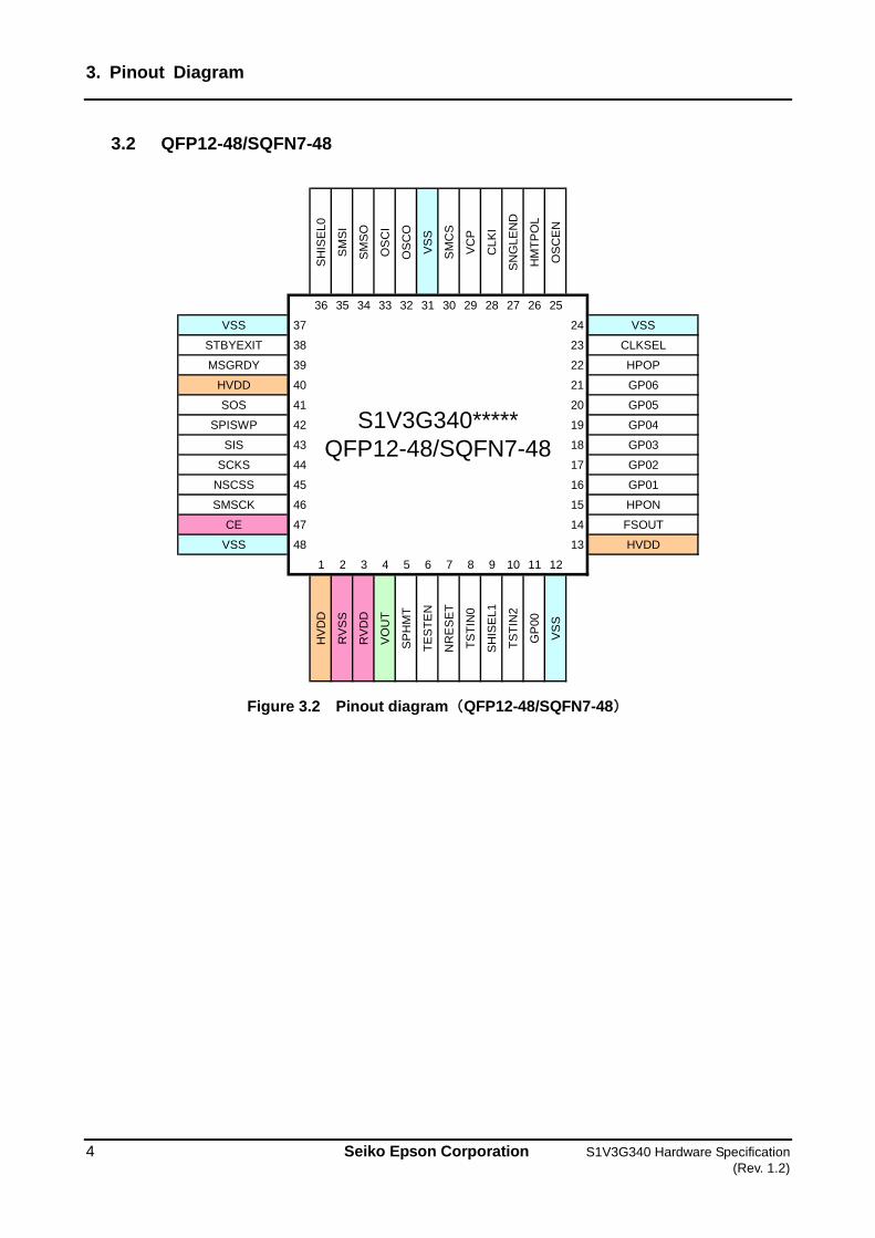
3.2 QFP12-48/SQFN7-48
SH
ISE
L0
SM
SI
SM
SO
OS
CI
OS
CO
VS
S
SM
CS
VC
P
CLK
I
SN
GLE
ND
HM
TPO
L
OS
CE
N
36 35 34 33 32 31 30 29 28 27 26 25
VSS 37 24 VSS
STBYEXIT 38 23 CLKSEL
MSGRDY 39 22 HPOP
HVDD 40 21 GP06
SOS 41 20 GP05
SPISWP 42 19 GP04
SIS 43 18 GP03
SCKS 44 17 GP02
NSCSS 45 16 GP01
SMSCK 46 15 HPON
CE 47 14 FSOUT
VSS 48 13 HVDD
1 2 3 4 5 6 7 8 9 10 11 12
HV
DD
RV
SS
RV
DD
VO
UT
SP
HM
T
TES
TEN
NR
ES
ET
TSTI
N0
SH
ISE
L1
TSTI
N2
GP
00
VS
S
S1V3G340*****QFP12-48/SQFN7-48
Figure 3.2 Pinout diagram(QFP12-48/SQFN7-48)
4. Pin Description
S1V3G340 Hardware Specification Seiko Epson Corporation 5 (Rev. 1.2)
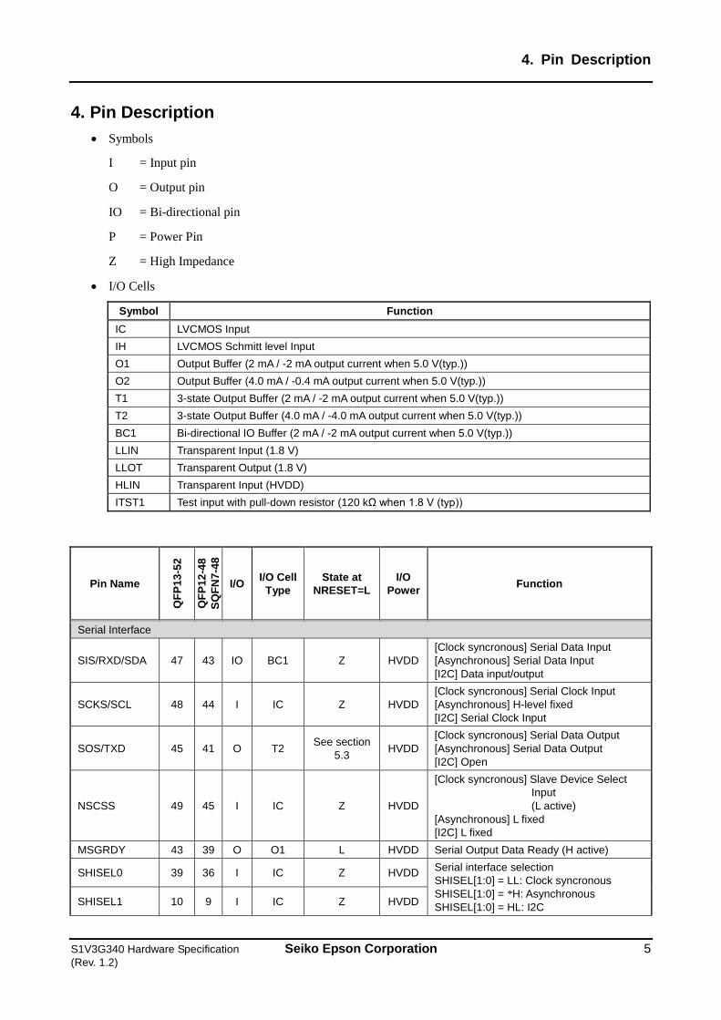
4. Pin Description • Symbols
I = Input pin
O = Output pin
IO = Bi-directional pin
P = Power Pin
Z = High Impedance
• I/O Cells
Symbol Function IC LVCMOS Input IH LVCMOS Schmitt level Input O1 Output Buffer (2 mA / -2 mA output current when 5.0 V(typ.)) O2 Output Buffer (4.0 mA / -0.4 mA output current when 5.0 V(typ.)) T1 3-state Output Buffer (2 mA / -2 mA output current when 5.0 V(typ.)) T2 3-state Output Buffer (4.0 mA / -4.0 mA output current when 5.0 V(typ.)) BC1 Bi-directional IO Buffer (2 mA / -2 mA output current when 5.0 V(typ.)) LLIN Transparent Input (1.8 V) LLOT Transparent Output (1.8 V) HLIN Transparent Input (HVDD) ITST1 Test input with pull-down resistor (120 kΩ when 1.8 V (typ))
Pin Name
QFP
13-5
2
QFP
12-4
8 SQ
FN7-
48
I/O I/O Cell Type
State at NRESET=L
I/O Power Function
Serial Interface
SIS/RXD/SDA 47 43 IO BC1 Z HVDD [Clock syncronous] Serial Data Input [Asynchronous] Serial Data Input [I2C] Data input/output
SCKS/SCL 48 44 I IC Z HVDD [Clock syncronous] Serial Clock Input [Asynchronous] H-level fixed [I2C] Serial Clock Input
SOS/TXD 45 41 O T2 See section 5.3 HVDD
[Clock syncronous] Serial Data Output [Asynchronous] Serial Data Output [I2C] Open
NSCSS 49 45 I IC Z HVDD
[Clock syncronous] Slave Device Select Input (L active)
[Asynchronous] L fixed [I2C] L fixed
MSGRDY 43 39 O O1 L HVDD Serial Output Data Ready (H active)
SHISEL0 39 36 I IC Z HVDD Serial interface selection SHISEL[1:0] = LL: Clock syncronous SHISEL[1:0] = *H: Asynchronous SHISEL[1:0] = HL: I2C SHISEL1 10 9 I IC Z HVDD
4. Pin Description
6 Seiko Epson Corporation S1V3G340 Hardware Specification (Rev. 1.2)
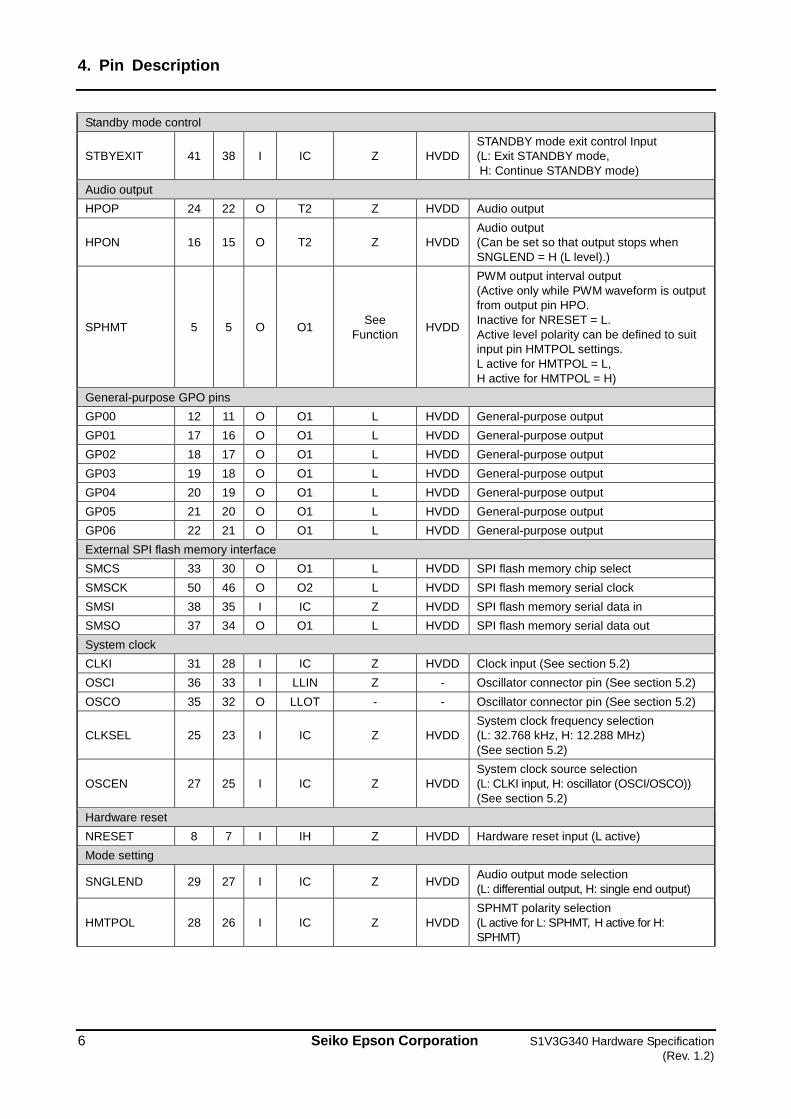
Standby mode control
STBYEXIT 41 38 I IC Z HVDD STANDBY mode exit control Input (L: Exit STANDBY mode, H: Continue STANDBY mode)
Audio output HPOP 24 22 O T2 Z HVDD Audio output
HPON 16 15 O T2 Z HVDD Audio output (Can be set so that output stops when SNGLEND = H (L level).)
SPHMT 5 5 O O1 See Function HVDD
PWM output interval output (Active only while PWM waveform is output from output pin HPO. Inactive for NRESET = L. Active level polarity can be defined to suit input pin HMTPOL settings. L active for HMTPOL = L, H active for HMTPOL = H)
General-purpose GPO pins GP00 12 11 O O1 L HVDD General-purpose output GP01 17 16 O O1 L HVDD General-purpose output GP02 18 17 O O1 L HVDD General-purpose output GP03 19 18 O O1 L HVDD General-purpose output GP04 20 19 O O1 L HVDD General-purpose output GP05 21 20 O O1 L HVDD General-purpose output GP06 22 21 O O1 L HVDD General-purpose output External SPI flash memory interface SMCS 33 30 O O1 L HVDD SPI flash memory chip select SMSCK 50 46 O O2 L HVDD SPI flash memory serial clock SMSI 38 35 I IC Z HVDD SPI flash memory serial data in SMSO 37 34 O O1 L HVDD SPI flash memory serial data out System clock CLKI 31 28 I IC Z HVDD Clock input (See section 5.2) OSCI 36 33 I LLIN Z - Oscillator connector pin (See section 5.2) OSCO 35 32 O LLOT - - Oscillator connector pin (See section 5.2)
CLKSEL 25 23 I IC Z HVDD System clock frequency selection (L: 32.768 kHz, H: 12.288 MHz) (See section 5.2)
OSCEN 27 25 I IC Z HVDD System clock source selection (L: CLKI input, H: oscillator (OSCI/OSCO)) (See section 5.2)
Hardware reset NRESET 8 7 I IH Z HVDD Hardware reset input (L active) Mode setting
SNGLEND 29 27 I IC Z HVDD Audio output mode selection (L: differential output, H: single end output)
HMTPOL 28 26 I IC Z HVDD SPHMT polarity selection (L active for L: SPHMT, H active for H: SPHMT)

4. Pin Description
S1V3G340 Hardware Specification Seiko Epson Corporation 7 (Rev. 1.2)
Test input/output
TESTEN 6 6 I ITST1 Pull-down - Test pin (Connected to VSS during normal operations)
VCP 32 29 O LLOT - - Test pin (Open during normal operations)
TSTIN2 11 10 I IC Z HVDD Test pin (Connected to VSS during normal operations)
TSTIN0 9 8 I IC Z HVDD Test pin (Connected to VSS during normal operations)
FSOUT 15 14 O T1 Z HVDD Test pin (Open during normal operations)
SPISWP 46 42 I IC Z HVDD Test pin (Connected to VSS during normal operations)
Internal voltage drop regulator
CE 51 47 I HLIN Z HVDD Test pin (Connected to HVDD during normal operations)
VOUT 4 4 O - - -
Internal voltage drop regulator output pin (1.8 V) (Connect 1 µF capacitor between VOUT and RVSS.)
Pin name QFP13-52 QFP12-48/SQFN7-48 I/O Function Power supply HVDD 1, 14, 30, 44 1,13,40 P IO cell power supply VSS 13, 26, 34, 40, 52 12, 24, 31, 37, 48 P Internal area and IO cell GND
RVDD 3 3 P Internal voltage drop regulator power supply
RVSS 2 2 P Internal voltage drop regulator GND Unused pins NC 7, 23, 42, - NC Unused pins

5. Function Description
8 Seiko Epson Corporation S1V3G340 Hardware Specification (Rev. 1.2)
5. Function Description
5.1 Standard Application System
Figure 5.1 Standard application system
Figure 5.1 shows a standard S1V3G340 application system. The host controls the S1V3G340 with commands (message protocol) issued via the serial interface. After Power On Reset, the S1V3G340 outputs audio from the internal DA converter while performing internal processing including decoding of the audio data from the SPI flash memory and the compressed audio data transmitted from the host.
For more information on commands, see “S1V3034x Series Message Protocol Specification.”
For more information on voice guidance creation tools, see “EPSON Speech IC Voice Guidance Creation Tool User Guide.”
Serial I/F
(SPI/UART/I2C)
SPI master I/F
Command controller
DA converter
Host
32.768kHz or 12.288MHz
Audio decoder
SRAM
ROM
2.2 V to 5.5 V
Clock or CERALOCK
Power supply voltage
Speaker
SPI FLASH memory
GPO x 7

5. Function Description
S1V3G340 Hardware Specification Seiko Epson Corporation 9 (Rev. 1.2)
5.2 System Clock The S1V3G340 system clock frequency can be set to either 32.768 kHz or 12.288 MHz. The clock source can be set to be either direct input (input from CLKI pin) or oscillator (connected to OSCI/OSCO pin). Note that only 32.768 kHz oscillators can be used. The frequency and clock source settings are defined by the input pin CLKSEL and OSCEN settings. Table 5.1 shows system clock mode settings.
Table 5.1 System clock mode settings
Mode setting Clock frequency
Clock pin settings CLKSEL OSCEN CLKI OSCI OSCO
0 0 32.768 kHz 32.768 kHz input L level input Open
0 1 32.768 kHz L level input Connect 32.768 kHz oscillator
1 0 12.288 MHz 12.288 MHz input L level input Open
1 1 12.288 MHz Must not be selected.

5. Function Description
10 Seiko Epson Corporation S1V3G340 Hardware Specification (Rev. 1.2)
5.3 Serial Interface The S1V3G340 serial interface can be set to clock synchronous, asynchronous (UART), or I2C.
• Clock synchronous
Supports slave mode.
Data length: 8-bit, fixed, MSB first
• Asynchronous (UART)
Data length: 8-bit, fixed, LSB first
Start bit: 1-bit, fixed
Stop bit: 1-bit or 2-bit, selectable (default: 1-bit)
Parity bit: Even, odd, or none, selectable (default: none)
Baud rate [bps]: 460 k, 230 k, 115 k, 57.6 k, 38.4 k, 19.2 k, 9.6 k (default: 9.6 kbps)
• I2C
Supports I2C slave mode.
Maximum transfer speed: 83.3 kHz (when I2C bus rising time is 480 ns or less)
Serial interface selection is defined by the input pin SHISEL[1:0] settings.
Table 5.2 lists serial interface mode settings.
Table 5.2 Serial interface mode settings
SHISEL Interface
Serial interface pin settings 1 0 SCKS SIS SOS NSCSS
0 0 Clock synchronous Serial clock input Data input Data output
Slave selection
input 0 1
UART H-level input Data input Data output L-level input 1 1
1 0 I2C Serial clock input Data input/output (Open) L-level input

5. Function Description
S1V3G340 Hardware Specification Seiko Epson Corporation 11 (Rev. 1.2)
Table 5.3 shows the pin states when hardware resetting is enabled (NRESET=L).
Table 5.3 States when hardware resetting is enabled (serial interface)
SHISEL Interface
States for NRESET=L (L: L-level output, H: H-level output, Z; High-impedance)
1 0 SCKS SIS SOS NSCSS
0 0 Clock synchronous Z Z
Dependent on NSCSS input level
L (when NSCSS = L) Z (when NSCSS = H)
Z
0 1 UART Z Z H Z
1 1 1 0 I2C Z Z Z Z
Note:
• The asynchronous serial interface (UART) is not available when the selected system clock frequency is 12.288 MHz.
• The maximum transfer speed of the I2C interface is 83.3 kHz. This maximum transfer speed is based on the I2C bus rising time of 480 ns or less. It should be noted that the maximum transfer speed will be lower if the I2C bus rising time exceeds 480 ns due to the load capacity and pull-up resistance.
• When using the I2C interface, it is recommended to use the sequence playback.
6. Electrical Characteristics
12 Seiko Epson Corporation S1V3G340 Hardware Specification (Rev. 1.2)
6. Electrical Characteristics
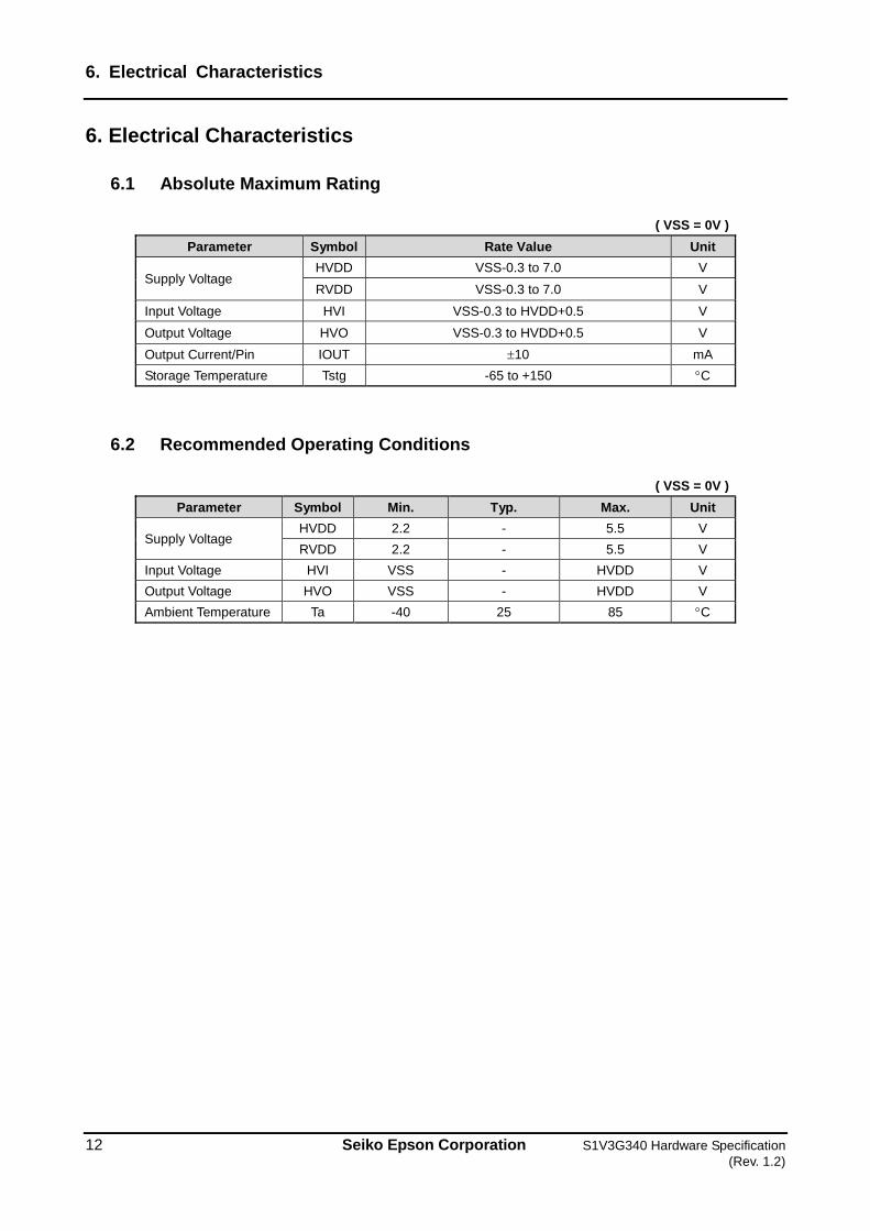
6.1 Absolute Maximum Rating
( VSS = 0V ) Parameter Symbol Rate Value Unit
Supply Voltage HVDD VSS-0.3 to 7.0 V RVDD VSS-0.3 to 7.0 V
Input Voltage HVI VSS-0.3 to HVDD+0.5 V Output Voltage HVO VSS-0.3 to HVDD+0.5 V Output Current/Pin IOUT ±10 mA Storage Temperature Tstg -65 to +150 °C
6.2 Recommended Operating Conditions
( VSS = 0V ) Parameter Symbol Min. Typ. Max. Unit
Supply Voltage HVDD 2.2 - 5.5 V RVDD 2.2 - 5.5 V
Input Voltage HVI VSS - HVDD V Output Voltage HVO VSS - HVDD V Ambient Temperature Ta -40 25 85 °C
6. Electrical Characteristics
S1V3G340 Hardware Specification Seiko Epson Corporation 13 (Rev. 1.2)
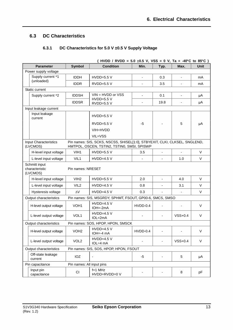
6.3 DC Characteristics
6.3.1 DC Characteristics for 5.0 V ±0.5 V Supply Voltage
( HVDD / RVDD = 5.0 ±0.5 V, VSS = 0 V, Ta = -40°C to 85°C )
Parameter Symbol Condition Min. Typ. Max. Unit Power supply voltage
Supply current *1 (unloaded)
IDDH HVDD=5.5 V - 0.3 - mA
IDDR RVDD=5.5 V - 3.5 - mA Static current
Supply current *2 IDDSH VIN = HVDD or VSS HVDD=5.5 V RVDD=5.5 V
- 0.1 - μA
IDDSR - 19.8 - μA
Input leakage current
Input leakage current HVDD=5.5 V
RVDD=5.5 V -5 - 5 μA
VIH=HVDD
VIL=VSS Input Characteristics (LVCMOS)
Pin names: SIS, SCKS, NSCSS, SHISEL[1:0], STBYEXIT, CLKI, CLKSEL, SNGLEND, HMTPOL, OSCEN, TSTIN2, TSTIN0, SMSI, SPISWP
H-level input voltage VIH1 HVDD=5.5 V 3.5 - - V
L-level input voltage VIL1 HVDD=4.5 V - - 1.0 V Schmitt input characteristic (LVCMOS)
Pin names: NRESET
H-level input voltage VIH2 HVDD=5.5 V 2.0 - 4.0 V
L-level input voltage VIL2 HVDD=4.5 V 0.8 - 3.1 V
Hysteresis voltage ∆V HVDD=4.5 V 0.3 - - V
Output characteristics Pin names: SIS, MSGRDY, SPHMT, FSOUT, GP00-6, SMCS, SMSO
H-level output voltage VOH1 HVDD=4.5 V IOH=-2mA HVDD-0.4 - - V
L-level output voltage VOL1 HVDD=4.5 V IOL=2mA - - VSS+0.4 V
Output characteristics Pin names: SOS, HPOP, HPON, SMSCK
H-level output voltage VOH2 HVDD=4.5 V IOH=-4 mA HVDD-0.4 - - V
L-level output voltage VOL2 HVDD=4.5 V IOL=4 mA - - VSS+0.4 V
Output characteristics Pin names: SIS, SOS, HPOP, HPON, FSOUT
Off-state leakage current IOZ - -5 - 5 μA
Pin capacitance Pin names: All input pins
Input pin capacitance CI f=1 MHz
HVDD=RVDD=0 V - - 8 pF

6. Electrical Characteristics
14 Seiko Epson Corporation S1V3G340 Hardware Specification (Rev. 1.2)
Pin capacitance Pin names: All output pins
Output pin capacitance CO f=1 MHz
HVDD=RVDD=0V - - 8 pF
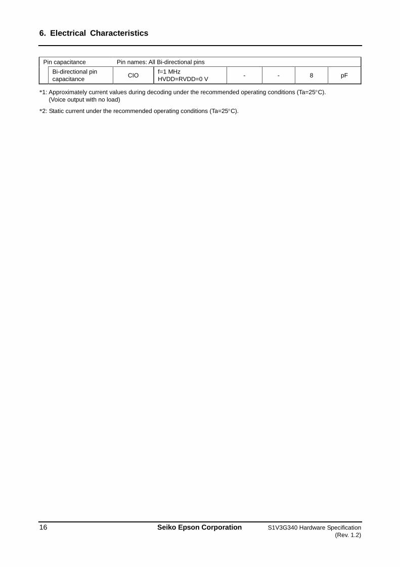
Pin capacitance Pin names: All Bi-directional pins
Bi-directional pin capacitance CIO f=1 MHz
HVDD=RVDD=0 V - - 8 pF
*1: Approximately current values during decoding under the recommended operating conditions (Ta=25°C). (Voice output with no load)
*2: Static current under the recommended operating conditions (Ta=25°C).

6. Electrical Characteristics
S1V3G340 Hardware Specification Seiko Epson Corporation 15 (Rev. 1.2)
6.3.2 DC Characteristics for 3.3 V ±0.3 V Supply Voltage
( HVDD / RVDD = 3.3 ±0.3 V, VSS = 0 V, Ta = -40°C to 85°C )
Parameter Symbol Condition Min. Typ. Max. Unit Power supply voltage
Supply current *1 (unloaded)
IDDH HVDD=3.3 V - 0.2 - mA
IDDR RVDD=3.3 V - 3.5 - mA Static current
Supply current *2 IDDSH VIN = HVDD or VSS HVDD=3.3 V RVDD=3.3 V
- 0.1 - μA
IDDSR - 17.9 - μA
Input leakage current
Input leakage current HVDD=3.6 V
RVDD=3.6 V -5 - 5 μA
VIH=HVDD
VIL=VSS Input Characteristics (LVCMOS)
Pin names: SIS, SCKS, NSCSS, SHISEL[1:0], STBYEXIT, CLKI, CLKSEL, SNGLEND, HMTPOL, OSCEN, TSTIN2, TSTIN0, SMSI, SPISWP
H-level input voltage VIH1 HVDD=3.6 V 2.2 - - V
L-level input voltage VIL1 HVDD=3.0 V - - 0.8 V
Schmitt input characteristic (LVCMOS)
Pin names: NRESET
H-level input voltage VIH2 HVDD=3.6 V 1.2 - 2.52 V
L-level input voltage VIL2 HVDD=3.0 V 0.75 - 1.98 V
Hysteresis voltage ∆V HVDD=3.0 V 0.3 - - V
Output characteristics Pin names: SIS, MSGRDY, SPHMT, FSOUT, GP00-6, SMCS, SMSO
H-level output voltage VOH1 HVDD=3.0 V IOH=-1.4 mA HVDD-0.4 - - V
L-level output voltage VOL1 HVDD=3.0 V IOL=1.4 mA - - VSS+0.4 V
Output characteristics Pin names: SOS, HPOP, HPON, SMSCK
H-level output voltage VOH2 HVDD=3.0 V IOH=-2.8 mA HVDD-0.4 - - V
L-level output voltage VOL2 HVDD=3.0 V IOL=2.8 mA - - VSS+0.4 V
Output characteristics Pin names: SIS, SOS, HPOP, HPON, FSOUT
Off-state leakage current IOZ - -5 - 5 μA
Pin capacitance Pin names: All input pins
Input pin capacitance CI f=1 MHz
HVDD=RVDD=0 V - - 8 pF
Pin capacitance Pin names: All output pins
Output pin capacitance CO f=1 MHz
HVDD=RVDD=0 V - - 8 pF
6. Electrical Characteristics
16 Seiko Epson Corporation S1V3G340 Hardware Specification (Rev. 1.2)
Pin capacitance Pin names: All Bi-directional pins
Bi-directional pin capacitance CIO f=1 MHz
HVDD=RVDD=0 V - - 8 pF
*1: Approximately current values during decoding under the recommended operating conditions (Ta=25°C). (Voice output with no load)
*2: Static current under the recommended operating conditions (Ta=25°C).
6. Electrical Characteristics
S1V3G340 Hardware Specification Seiko Epson Corporation 17 (Rev. 1.2)
6.3.3 DC Characteristics for 2.4 V ±0.2 V Supply Voltage
( HVDD / RVDD = 2.4 ±0.2 V, VSS = 0 V, Ta = -40°C to 85°C )
Parameter Symbol Condition Min. Typ. Max. Unit Power supply voltage
Supply current *1 (unloaded)
IDDH HVDD=2.2 V - 0.1 - mA
IDDR RVDD=2.2 V - 3.5 - mA
Static current
Supply current *2 IDDSH VIN = HVDD or VSS HVDD=2.2 V RVDD=2.2 V
- 0.1 - μA
IDDSR - 17.5 - μA
Input leakage current Input leakage current HVDD=2.4 V
RVDD=2.4 V -5 - 5 μA
VIH=HVDD
VIL=VSS Input Characteristics (LVCMOS)
Pin names: SIS, SCKS, NSCSS, SHISEL[1:0], STBYEXIT, CLKI, CLKSEL, SNGLEND, HMTPOL, OSCEN, TSTIN2, TSTIN0, SMSI, SPISWP
H-level input voltage VIH1 HVDD=2.6 V 1.6 - - V
L-level input voltage VIL1 HVDD=2.2 V - - 0.6 V Schmitt input characteristic (LVCMOS)
Pin names: NRESET
H-level input voltage VIH2 HVDD=2.6 V 0.88 - 1.82 V
L-level input voltage VIL2 HVDD=2.2 V 0.55 - 1.43 V
Hysteresis voltage ∆V HVDD=2.2 V 0.22 - - V
Output characteristics Pin names: SIS, MSGRDY, SPHMT, FSOUT, GP00-GP06, SMCS, SMSO
H-level output voltage VOH1 HVDD=2.2 V IOH=-1.0 mA HVDD-0.4 - - V
L-level output voltage VOL1 HVDD=2.2 V IOL=1.0 mA - - VSS+0.4 V
Output characteristics Pin names: SOS, HPOP, HPON, SMSCK
H-level output voltage VOH2 HVDD=2.2 V IOH=-2.0 mA HVDD-0.4 - - V
L-level output voltage VOL2 HVDD=2.2 V IOL=2.0 mA - - VSS+0.4 V
Output characteristics Pin names: SIS, SOS, HPOP, HPON, FSOUT
Off-state leakage current IOZ - -5 - 5 μA
Pin capacitance Pin names: All input pins
Input pin capacitance CI f=1 MHz
HVDD=RVDD=0 V - - 8 pF
Pin capacitance Pin names: All output pins
Output pin capacitance CO f=1MHz
HVDD=RVDD=0 V - - 8 pF

6. Electrical Characteristics
18 Seiko Epson Corporation S1V3G340 Hardware Specification (Rev. 1.2)
Pin capacitance Pin names: All Bi-directional pins
Bi-directional pin capacitance CIO f=1 MHz
HVDD=RVDD=0 V - - 8 pF
*1: Approximately current values during decoding under the recommended operating conditions (Ta=25°C). (Voice output with no load)
*2: Static current under the recommended operating conditions (Ta=25°C).
6. Electrical Characteristics
S1V3G340 Hardware Specification Seiko Epson Corporation 19 (Rev. 1.2)
6.4 AC Characteristics
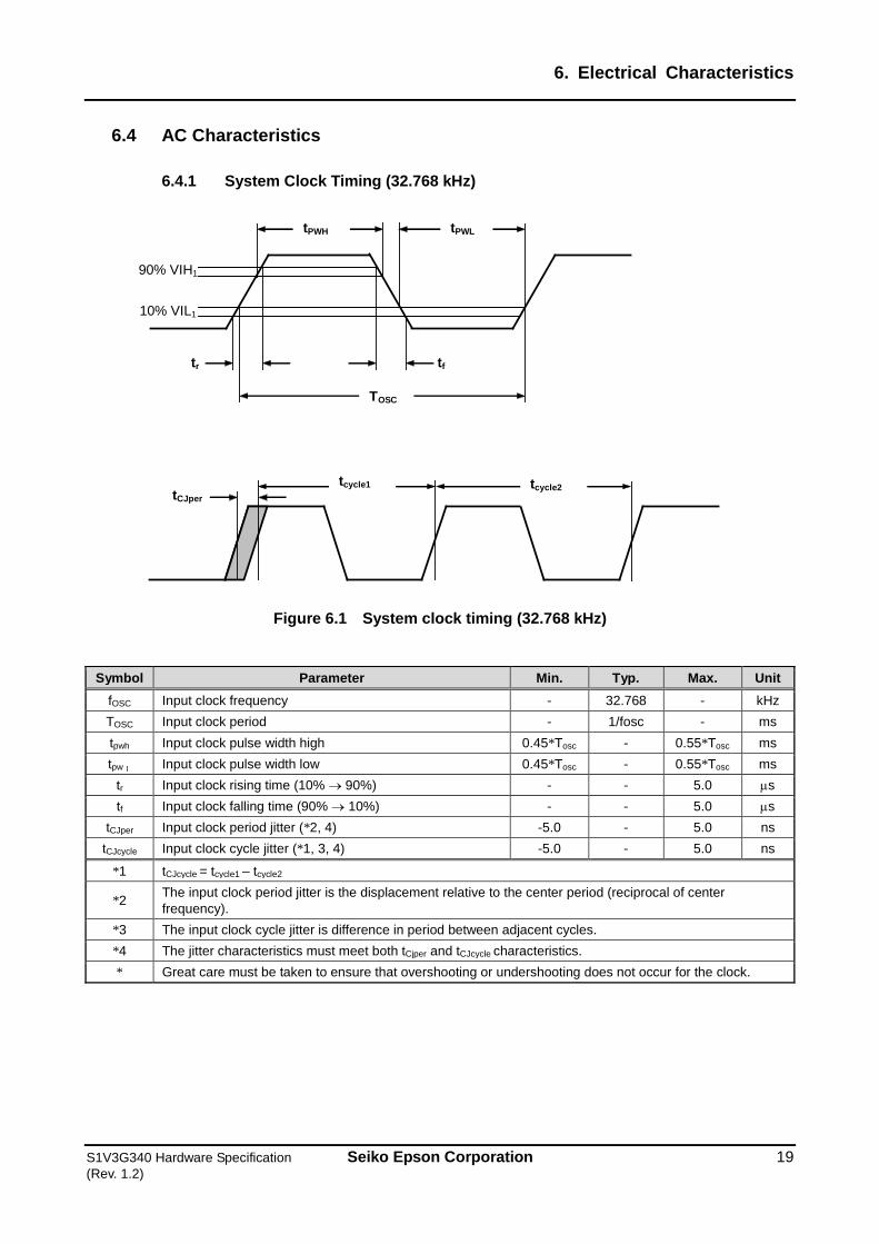
6.4.1 System Clock Timing (32.768 kHz)
90% VIH1
10% VIL1
tPWH tPWL
tr tf
TOSC
tCJper tcycle1 tcycle2
Figure 6.1 System clock timing (32.768 kHz)
Symbol Parameter Min. Typ. Max. Unit fOSC Input clock frequency - 32.768 - kHz TOSC Input clock period - 1/fosc - ms tpwh Input clock pulse width high 0.45*Tosc - 0.55*Tosc ms tpwl Input clock pulse width low 0.45*Tosc - 0.55*Tosc ms
tr Input clock rising time (10% → 90%) - - 5.0 µs tf Input clock falling time (90% → 10%) - - 5.0 µs
tCJper Input clock period jitter (*2, 4) -5.0 - 5.0 ns tCJcycle Input clock cycle jitter (*1, 3, 4) -5.0 - 5.0 ns
*1 tCJcycle = tcycle1 – tcycle2
*2 The input clock period jitter is the displacement relative to the center period (reciprocal of center frequency).
*3 The input clock cycle jitter is difference in period between adjacent cycles. *4 The jitter characteristics must meet both tCjper and tCJcycle characteristics. * Great care must be taken to ensure that overshooting or undershooting does not occur for the clock.
6. Electrical Characteristics
20 Seiko Epson Corporation S1V3G340 Hardware Specification (Rev. 1.2)
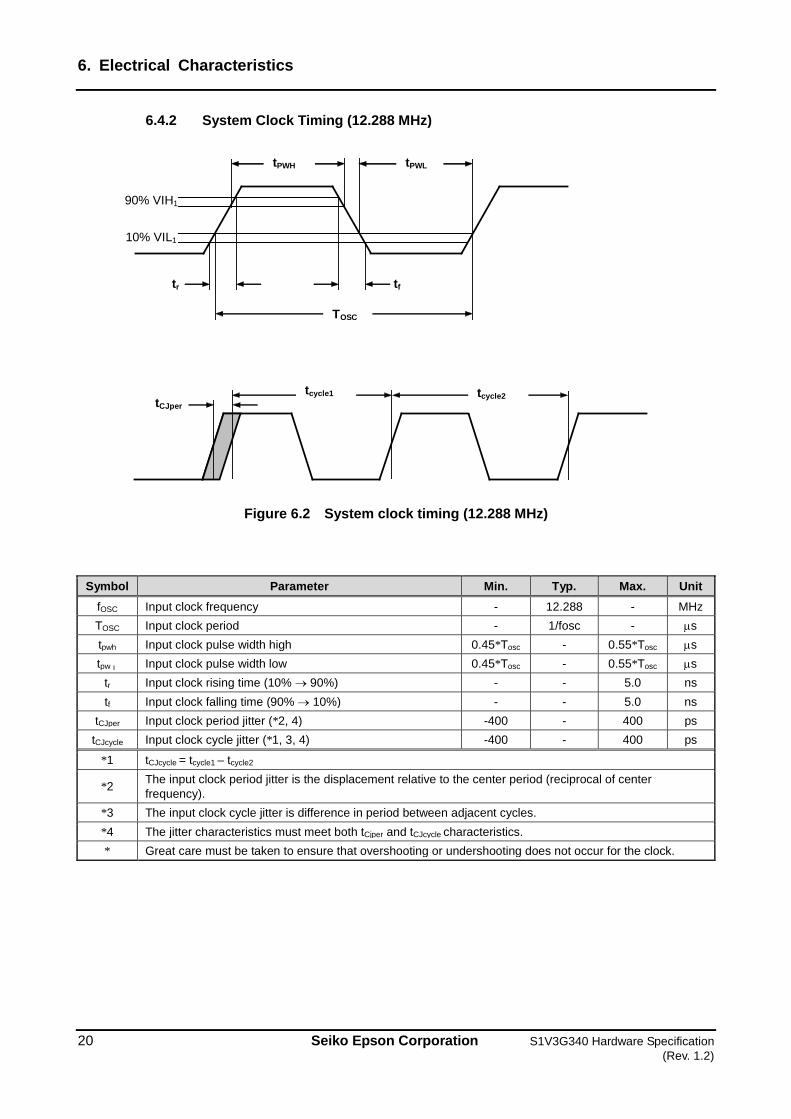
6.4.2 System Clock Timing (12.288 MHz)
90% VIH1
10% VIL1
tPWH tPWL
tr tf
TOSC
tCJper tcycle1 tcycle2
Figure 6.2 System clock timing (12.288 MHz)
Symbol Parameter Min. Typ. Max. Unit fOSC Input clock frequency - 12.288 - MHz TOSC Input clock period - 1/fosc - µs tpwh Input clock pulse width high 0.45*Tosc - 0.55*Tosc µs tpwl Input clock pulse width low 0.45*Tosc - 0.55*Tosc µs
tr Input clock rising time (10% → 90%) - - 5.0 ns tf Input clock falling time (90% → 10%) - - 5.0 ns
tCJper Input clock period jitter (*2, 4) -400 - 400 ps tCJcycle Input clock cycle jitter (*1, 3, 4) -400 - 400 ps
*1 tCJcycle = tcycle1 – tcycle2
*2 The input clock period jitter is the displacement relative to the center period (reciprocal of center frequency).
*3 The input clock cycle jitter is difference in period between adjacent cycles. *4 The jitter characteristics must meet both tCjper and tCJcycle characteristics. * Great care must be taken to ensure that overshooting or undershooting does not occur for the clock.

6. Electrical Characteristics
S1V3G340 Hardware Specification Seiko Epson Corporation 21 (Rev. 1.2)
6.4.3 Power-on / Reset Timing
HVDD RVDD
NRESET
CLKI / OSCI
t2
t1
t3 t3
Figure 6.3 Power on / reset timing
Symbol Item Min. Typ Max. Unit
t1
Minimum delay from the HVDD power-on to the CLKI/OSCI rising edge before NRESET release.
Input clock source: CLKI 100 - - μs
Input clock source: OSCI *2 - 1 - s
t2 The minimum NRESET assertion on system power up. 2 - - TOSC
(*1)
t3 NRESET synchronization time (Number of clock cycles before the reset signal is applied internally.) 2 - - TOSC
(*1)
*1 TOSC is the CLKI / OSCI clock period.
*2 Oscillation characteristics change depending on conditions such as components used (oscillator, Rf, Rd, Cg, Cd), board pattern, and rising time of supplied voltage. Use this characteristics as reference values.
Note: The circuit must be initialized with NRESET after initiating power supply. The internal circuit state cannot be guaranteed when switching the HVDD from off to on, due to power supply noise and other factors.
6. Electrical Characteristics
22 Seiko Epson Corporation S1V3G340 Hardware Specification (Rev. 1.2)
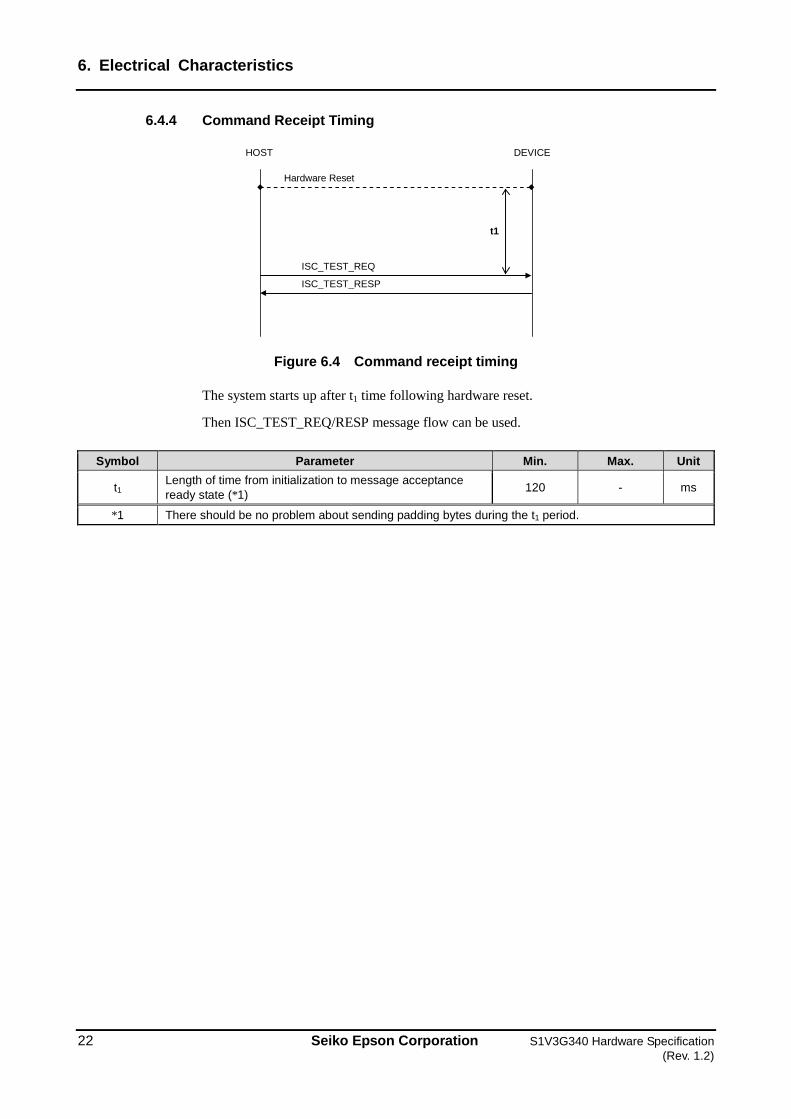
6.4.4 Command Receipt Timing
ISC_TEST_REQ
ISC_TEST_RESP
HOST DEVICE
t1
Hardware Reset
Figure 6.4 Command receipt timing
The system starts up after t1 time following hardware reset.
Then ISC_TEST_REQ/RESP message flow can be used.
Symbol Parameter Min. Max. Unit
t1 Length of time from initialization to message acceptance ready state (*1) 120 - ms
*1 There should be no problem about sending padding bytes during the t1 period.
6. Electrical Characteristics
S1V3G340 Hardware Specification Seiko Epson Corporation 23 (Rev. 1.2)
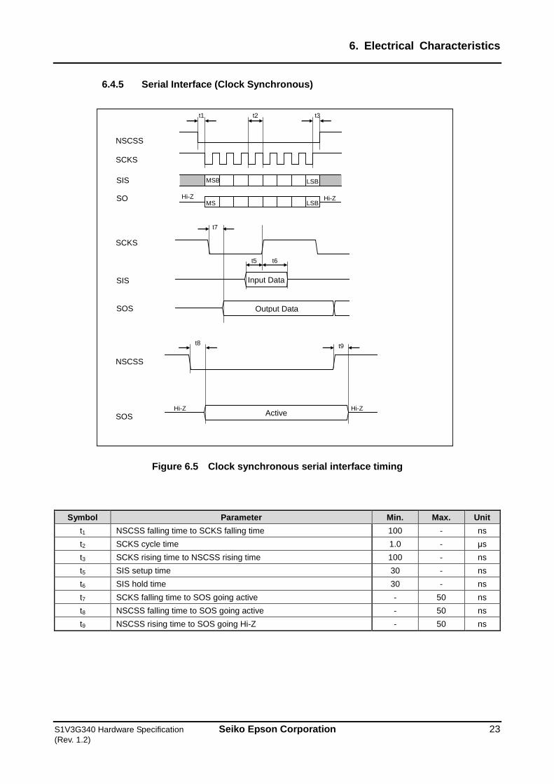
6.4.5 Serial Interface (Clock Synchronous)
SCKS
SIS
NSCSS
t5 t6
t7
SOS
t9
SOS Active Hi-Z
MSB LSB
MS
SIS
SO
NSCSS
t1 t3 t2
SCKS
Hi-Z Hi-Z LSB
Hi-Z
t8
Input Data
Output Data
Figure 6.5 Clock synchronous serial interface timing
Symbol Parameter Min. Max. Unit t1 NSCSS falling time to SCKS falling time 100 - ns t2 SCKS cycle time 1.0 - μs t3 SCKS rising time to NSCSS rising time 100 - ns t5 SIS setup time 30 - ns t6 SIS hold time 30 - ns t7 SCKS falling time to SOS going active - 50 ns t8 NSCSS falling time to SOS going active - 50 ns t9 NSCSS rising time to SOS going Hi-Z - 50 ns
6. Electrical Characteristics
24 Seiko Epson Corporation S1V3G340 Hardware Specification (Rev. 1.2)
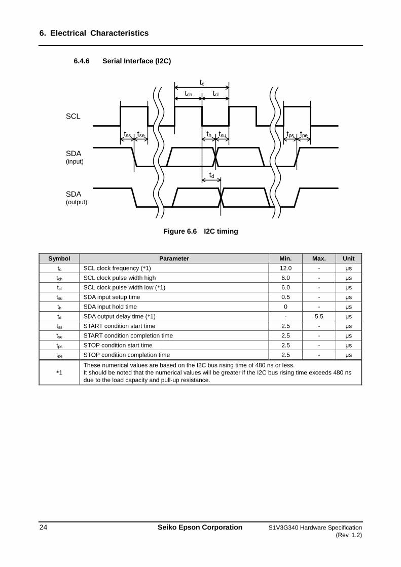
6.4.6 Serial Interface (I2C)
tctch tcl
th tsutss tse tps tpe
td
SCL
SDA(input)
SDA(output)
Figure 6.6 I2C timing
Symbol Parameter Min. Max. Unit tc SCL clock frequency (*1) 12.0 - μs tch SCL clock pulse width high 6.0 - μs tcl SCL clock pulse width low (*1) 6.0 - μs tsu SDA input setup time 0.5 - μs th SDA input hold time 0 - μs td SDA output delay time (*1) - 5.5 μs tss START condition start time 2.5 - μs tse START condition completion time 2.5 - μs tps STOP condition start time 2.5 - μs tpe STOP condition completion time 2.5 - μs
*1 These numerical values are based on the I2C bus rising time of 480 ns or less. It should be noted that the numerical values will be greater if the I2C bus rising time exceeds 480 ns due to the load capacity and pull-up resistance.
6. Electrical Characteristics
S1V3G340 Hardware Specification Seiko Epson Corporation 25 (Rev. 1.2)
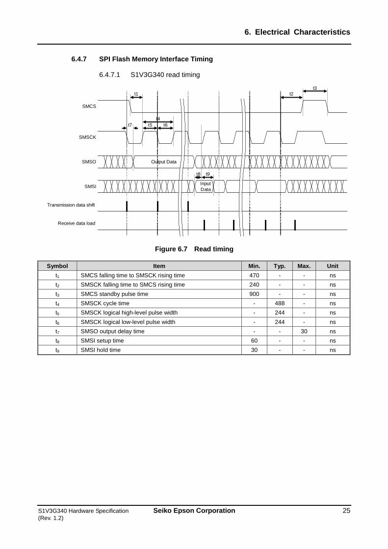
6.4.7 SPI Flash Memory Interface Timing
6.4.7.1 S1V3G340 read timing
SMCS
SMSCK
SMSO
SMSI
t1
t5 t6t7t4
t8 t9
Output Data
InputData
Transmission data shift
Receive data load
t2t3
Figure 6.7 Read timing
Symbol Item Min. Typ. Max. Unit t1 SMCS falling time to SMSCK rising time 470 - - ns t2 SMSCK falling time to SMCS rising time 240 - - ns t3 SMCS standby pulse time 900 - - ns t4 SMSCK cycle time - 488 - ns t5 SMSCK logical high-level pulse width - 244 - ns t6 SMSCK logical low-level pulse width - 244 - ns t7 SMSO output delay time - - 30 ns t8 SMSI setup time 60 - - ns t9 SMSI hold time 30 - - ns
6. Electrical Characteristics
26 Seiko Epson Corporation S1V3G340 Hardware Specification (Rev. 1.2)
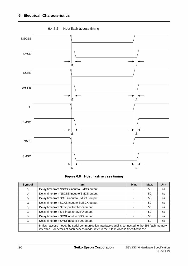
6.4.7.2 Host flash access timing
NSCSS
SMCS
SCKS
SMSCK
SIS
SMSO
SMSI
SMSO
t1 t2
t3 t4
t5 t6
t7 t8
Figure 6.8 Host flash access timing
Symbol Item Min. Max. Unit t1 Delay time from NSCSS input to SMCS output - 50 ns t2 Delay time from NSCSS input to SMCS output - 50 ns t3 Delay time from SCKS input to SMSCK output - 50 ns t4 Delay time from SCKS input to SMSCK output - 50 ns t5 Delay time from SIS input to SMSO output - 50 ns t6 Delay time from SIS input to SMSO output - 50 ns t7 Delay time from SMSI input to SOS output - 50 ns t8 Delay time from SMSI input to SOS output - 50 ns
In flash access mode, the serial communication interface signal is connected to the SPI flash memory interface. For details of flash access mode, refer to the “Flash Access Specifications.”
7. External Connection Examples
S1V3G340 Hardware Specification Seiko Epson Corporation 27 (Rev. 1.2)
7. External Connection Examples
7.1 System Clock The S1V3G340 system clock frequency can be set to either 32.768 kHz or 12.288 MHz. Likewise, the clock source can be set to either direct input (input from CLKI pin) or oscillator (connected to OSCI/OSCO pin). Note that only 32.768 kHz oscillators can be used. External connection examples are shown below for various clock supply configurations.
7.1.1 Direct Input
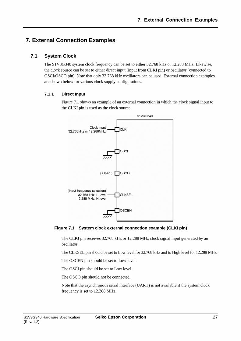
Figure 7.1 shows an example of an external connection in which the clock signal input to the CLKI pin is used as the clock source.
Figure 7.1 System clock external connection example (CLKI pin)
The CLKI pin receives 32.768 kHz or 12.288 MHz clock signal input generated by an oscillator.
The CLKSEL pin should be set to Low level for 32.768 kHz and to High level for 12.288 MHz.
The OSCEN pin should be set to Low level.
The OSCI pin should be set to Low level.
The OSCO pin should not be connected.
Note that the asynchronous serial interface (UART) is not available if the system clock frequency is set to 12.288 MHz.
7. External Connection Examples
28 Seiko Epson Corporation S1V3G340 Hardware Specification (Rev. 1.2)
7.1.2 Oscillator (32.768 kHz)
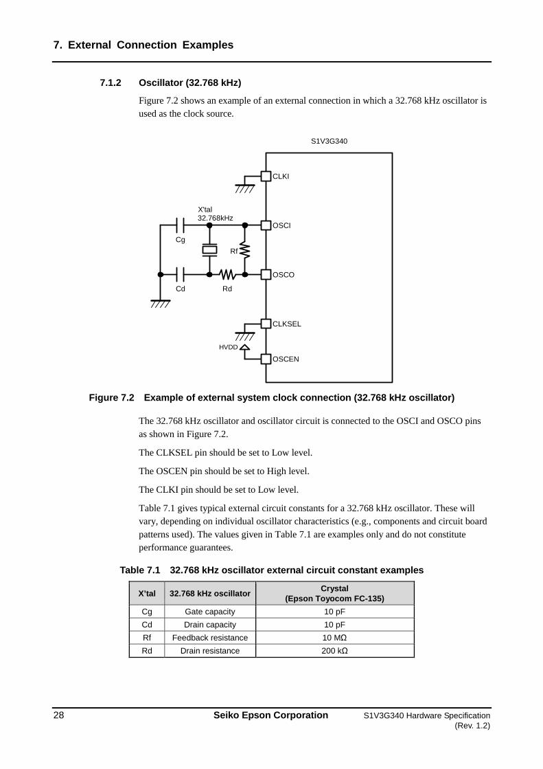
Figure 7.2 shows an example of an external connection in which a 32.768 kHz oscillator is used as the clock source.
Rf
RdCd
Cg
X'tal32.768kHz
HVDD
OSCO
OSCI
S1V3G340
CLKI
CLKSEL
OSCEN
Figure 7.2 Example of external system clock connection (32.768 kHz oscillator)
The 32.768 kHz oscillator and oscillator circuit is connected to the OSCI and OSCO pins as shown in Figure 7.2.
The CLKSEL pin should be set to Low level.
The OSCEN pin should be set to High level.
The CLKI pin should be set to Low level.
Table 7.1 gives typical external circuit constants for a 32.768 kHz oscillator. These will vary, depending on individual oscillator characteristics (e.g., components and circuit board patterns used). The values given in Table 7.1 are examples only and do not constitute performance guarantees.
Table 7.1 32.768 kHz oscillator external circuit constant examples
X’tal 32.768 kHz oscillator Crystal (Epson Toyocom FC-135)
Cg Gate capacity 10 pF Cd Drain capacity 10 pF Rf Feedback resistance 10 MΩ Rd Drain resistance 200 kΩ
7. External Connection Examples
S1V3G340 Hardware Specification Seiko Epson Corporation 29 (Rev. 1.2)
7.2 Serial Interface
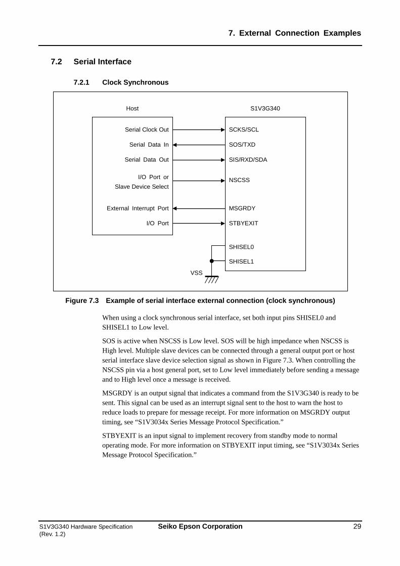
7.2.1 Clock Synchronous
Figure 7.3 Example of serial interface external connection (clock synchronous)
When using a clock synchronous serial interface, set both input pins SHISEL0 and SHISEL1 to Low level.
SOS is active when NSCSS is Low level. SOS will be high impedance when NSCSS is High level. Multiple slave devices can be connected through a general output port or host serial interface slave device selection signal as shown in Figure 7.3. When controlling the NSCSS pin via a host general port, set to Low level immediately before sending a message and to High level once a message is received.
MSGRDY is an output signal that indicates a command from the S1V3G340 is ready to be sent. This signal can be used as an interrupt signal sent to the host to warn the host to reduce loads to prepare for message receipt. For more information on MSGRDY output timing, see “S1V3034x Series Message Protocol Specification.”
STBYEXIT is an input signal to implement recovery from standby mode to normal operating mode. For more information on STBYEXIT input timing, see “S1V3034x Series Message Protocol Specification.”
Serial Clock Out
Serial Data In
Serial Data Out
I/O Port or Slave Device Select
SCKS/SCL
SOS/TXD
SIS/RXD/SDA
NSCSS
Host S1V3G340
External Interrupt Port MSGRDY
I/O Port STBYEXIT
SHISEL0
SHISEL1
VSS

7. External Connection Examples
30 Seiko Epson Corporation S1V3G340 Hardware Specification (Rev. 1.2)
7.2.2 Asynchronous (UART)
Figure 7.4 Serial interface external connection example (asynchronous)
When using an asynchronous serial interface (UART), the SHISEL0 input pin should be set to High level and SHISEL1 should be set to Low level. Note that the UART interface is not available when the system clock frequency is 12.288 MHz.
The initial interface settings are as shown below.
Start bit length: 1 bit
Stop bit length: 1 bit
Parity bit: None
Baud rate: 9.6 kbps
The interface settings can be changed using the ISC_UART_CONFIG_REQ message. Interface settings set via this message will be maintained until a hardware reset. A hardware reset restores interface settings to the initial default values shown above. The ISC_UART_CONFIG_REQ message can be used if necessary. For additional information, see “S1V3034x Series Message Protocol Specification.”
MSGRDY is an output signal indicating that a command to be sent from the S1V3G340 is ready to be sent. For more information on the data receiving flow on the host side and the MSGRDY output timing, see “S1V3034x Series Message Protocol Specification.”
STBYEXIT is an input signal used to implement recovery from standby mode to normal operating mode. For more information on the STBYEXIT input timing, see “S1V3034x Series Message Protocol Specification.”
Serial Data In
Serial Data Out
SCKS/SCL
SOS/TXD
SIS/RXD/SDA
NSCSS
Host S1V3G340
External Interrupt Port MSGRDY
I/O Port STBYEXIT
SHISEL0
SHISEL1
VSS
HVDD
HVDD
VSS

7. External Connection Examples
S1V3G340 Hardware Specification Seiko Epson Corporation 31 (Rev. 1.2)
7.2.3 I2C
Figure 7.5 Serial interface external connection example (I2C)
If I2C is used, set the SHISEL0 input pin to Low level and SHISEL1 to High level.
MSGRDY is an output signal indicating that a command to be sent from the S1V3G340 is ready to be sent. For more information on the data receiving flow on the host side and the MSGRDY output timing, see “S1V3034x Series Message Protocol Specification.”
STBYEXIT is an input signal used to implement recovery from standby mode to normal operating mode. For more information on the STBYEXIT input timing, see “S1V3034x Series Message Protocol Specification.”
SCL
SDA
SCKS/SCL
SOS/TXD
SIS/RXD/SDA
NSCSS
Host S1V3G340
External Interrupt Port MSGRDY
I/O Port STBYEXIT
SHISEL0
SHISEL1
VSS
HVDD
VSS
(Open)
8. Package Dimensions
32 Seiko Epson Corporation S1V3G340 Hardware Specification (Rev. 1.2)
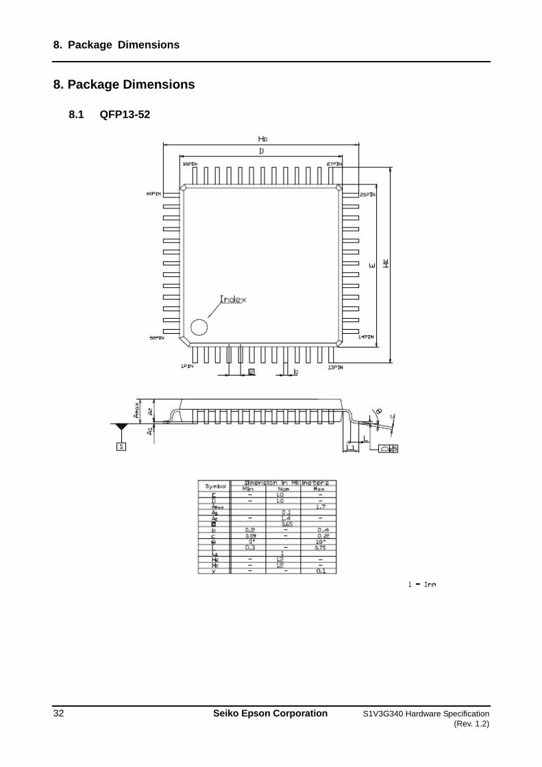
8. Package Dimensions
8.1 QFP13-52
8. Package Dimensions
S1V3G340 Hardware Specification Seiko Epson Corporation 33 (Rev. 1.2)
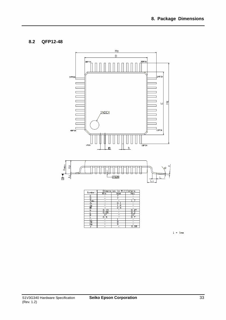
8.2 QFP12-48
8. Package Dimensions
34 Seiko Epson Corporation S1V3G340 Hardware Specification (Rev. 1.2)
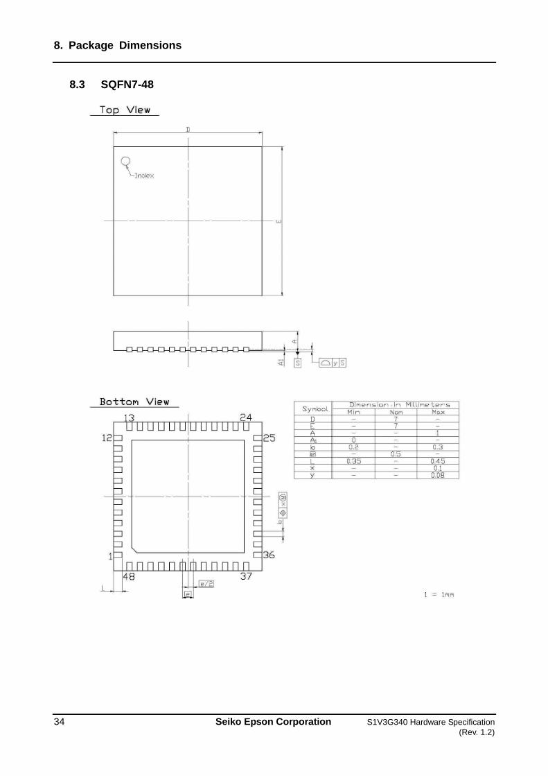
8.3 SQFN7-48
9. Reference Material
S1V3G340 Hardware Specification Seiko Epson Corporation 35 (Rev. 1.2)
9. Reference Material
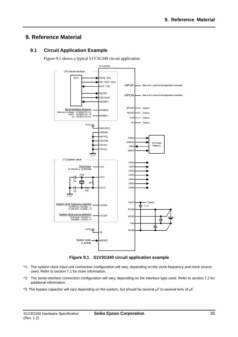
9.1 Circuit Application Example Figure 9.1 shows a typical S1V3G340 circuit application.
Figure 9.1 S1V3G340 circuit application example
*1: The system clock input unit connection configuration will vary, depending on the clock frequency and clock source used. Refer to section 7.1 for more information.
*2: The serial interface connection configuration will vary, depending on the interface type used. Refer to section 7.2 for additional information.
*3: The bypass capacitor will vary depending on the system, but should be several µF to several tens of µF.
HPOP
HPON
9. Reference Material
36 Seiko Epson Corporation S1V3G340 Hardware Specification (Rev. 1.2)
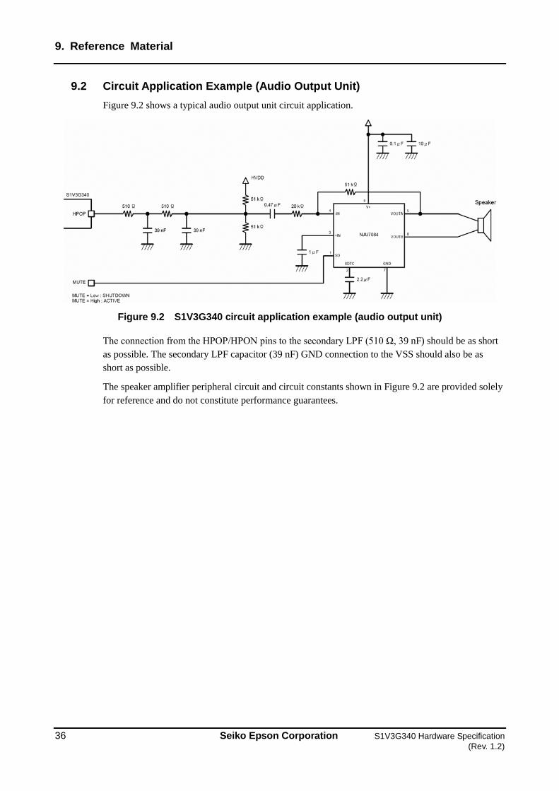
9.2 Circuit Application Example (Audio Output Unit) Figure 9.2 shows a typical audio output unit circuit application.
Figure 9.2 S1V3G340 circuit application example (audio output unit)
The connection from the HPOP/HPON pins to the secondary LPF (510 Ω, 39 nF) should be as short as possible. The secondary LPF capacitor (39 nF) GND connection to the VSS should also be as short as possible.
The speaker amplifier peripheral circuit and circuit constants shown in Figure 9.2 are provided solely for reference and do not constitute performance guarantees.

9. Reference Material
S1V3G340 Hardware Specification Seiko Epson Corporation 37 (Rev. 1.2)
9.3 Mute Start/Release Timing It is recommended to control the mute function of the speaker amplifier by using the general-purpose input/output port in order to minimize noise at power ON/OFF and in standby. The following shows an example of mute control timing in each operation condition.
9.3.1 System Reset Active ⇒ Release
NRESET
t1
MUTE
Symbol Item Min. Max. Unit t1 NRESET release time to MUTE release time 150 - ms
Note: In the above timing chart, the MUTE pin is at the Low level and MUTE is active.
9.3.2 Standby Mode
The following shows an example of the MUTE control flow before and after standby mode.
• Transition to standby mode MUTE enabled → STANDBY_ENTRY_REQ issued → STBYEXIT: High
• End of standby mode STBYEXIT: Low → STANDBY_EXIT_IND received → MUTE released
Note: In the above timing chart, the MUTE pin is at the Low level and MUTE is active.
* Refer to the Message Protocol Specification for details of standby mode.
Standby mode active period
MUTE
9. Reference Material
38 Seiko Epson Corporation S1V3G340 Hardware Specification (Rev. 1.2)
9.4 Power Supply Precautions Always initialize the circuit with NRESET after initiating power supply. The internal circuit state cannot be guaranteed when switching the HVDD from off to on due to power supply noise and other factors.
CMOS devices may suffer from what is known as “latch-up.” This is a phenomenon in which the PNPN bonds (thyristor configuration) inside the CMOS IC conduct, resulting in large currents between VDD and VSS and ultimately damaging the CMOS.
Latch-up occurs when the voltage applied to the input/output pins exceeds rated values, resulting in large currents within the component, or when the VDD pin voltage exceeds the ratings, causing internal components to yield. If the voltage exceeds the ratings even momentarily in these cases, a large current will arise between VDD and VSS once latch-up occurs, resulting in potential overheating and smoke generation. Always observe the following precautions:
(1) Never raise the input/output pin voltage level above the supply voltage or above the range specified for electrical characteristics. Avoid lowering below VSS.
(2) Make sure the device is not subject to abnormal noise.
(3) The potential for unused input pins should be pegged to VDD or VSS.
(4) Do not short-circuit the output.

9. Reference Material
S1V3G340 Hardware Specification Seiko Epson Corporation 39 (Rev. 1.2)
9.5 Clock direct input precautions Noise will be input to the power supply if the overshoot or undershoot in the clock is excessive when using an external direct clock input. This may cause the internal regulator output to fluctuate, possibly resulting in internal circuit damage or malfunction.
Clock overshoot and undershoot must be kept within the input voltage range indicated in Section “6.1 Absolute maximum rating.” If overshoot or undershoot is present, this should be addressed using a damping resistance or low pass filter.
The same prevention measures are required for external signals other than the clock external input, but particular caution is necessary for the clock due to the high frequency.
S1V3G340
CLKIClockGenerator
Dumping Resistance
Figure 9.3 Typical clock input overshoot/undershoot prevention measures
9. Reference Material
40 Seiko Epson Corporation S1V3G340 Hardware Specification (Rev. 1.2)
9.6 Precautions on Mounting The following shows the precautions when designing the board and mounting the IC.
9.6.1 Oscillation Circuit
Oscillation characteristics change depending on conditions such as components used (oscillator, Rf, Rd, Cg, Cd) and board pattern. In particular, when a ceramic or crystal oscillator is used, evaluate the components adequately under real operating conditions by mounting them on the board before the external resistor (Rf, Rd) and capacitor (Cg, Cd) values are finally decided.
Disurbances of the oscillation clock due to noise may cause a malfunction. To prevent this, the following points should be taken into consideration.
• Components that are connected to the OSCI and OSCO pins, such as oscillator, resistors and capacitors, should be connected in the shortest line.
• Whenever possible, configure digital signal lines with at least three millimeters clearance from the OSCI and OSCO and the components and lines connected to these pins. In particular, signals thet are switched frequently must not be placed near these pins, components, and lines. The same applies to all layers on the multi-layered board as the distance between the layers is around 0.1 to 0.2 mm. Furthermore, do not configure digital signal lines in parallel with these components and lines when arranging them on the same or another layer of the board. Such an arrangement is strictly prohibited, even with clearance of three millimeters or more. Also, avoid arranging digital signal lines across these components and signal lines.
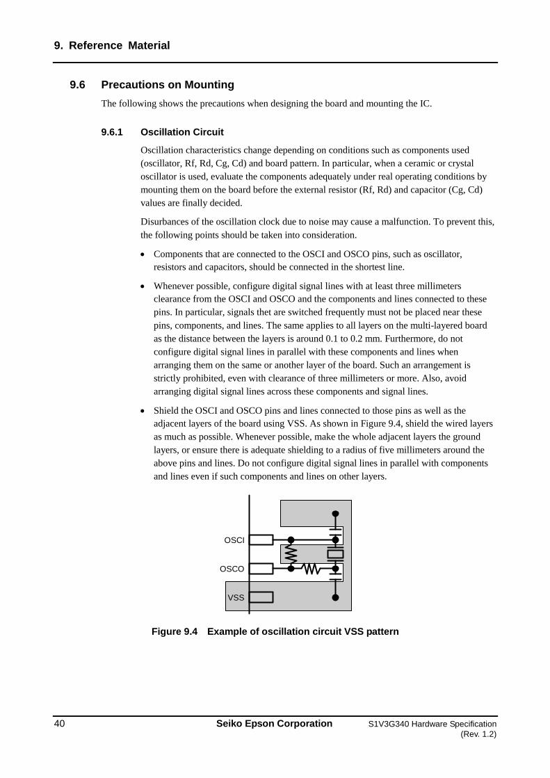
• Shield the OSCI and OSCO pins and lines connected to those pins as well as the adjacent layers of the board using VSS. As shown in Figure 9.4, shield the wired layers as much as possible. Whenever possible, make the whole adjacent layers the ground layers, or ensure there is adequate shielding to a radius of five millimeters around the above pins and lines. Do not configure digital signal lines in parallel with components and lines even if such components and lines on other layers.
VSS
OSCI
OSCO
Figure 9.4 Example of oscillation circuit VSS pattern
9. Reference Material
S1V3G340 Hardware Specification Seiko Epson Corporation 41 (Rev. 1.2)
9.6.2 Reset Circuit
The power-on reset signal which is input to the NRESET pin changes depending on conditions (power rise time, component used, board pattern, etc.). Decide the constant of the capacitor and resistor after enough tests have been completed with the apprication product. With regard to the pull-up resistance of the NRESET pin, if the impedance is high, noise can generate a malfunction; therefore, the constants must be determined in careful consideration of resistance value variations.
9.6.3 Power Supply Circuit
Sudden power supply variation due to noise may cause malfunction. Consider the following points to prevent this:
• The power supply should be connected to the HVDD/RVDD and VSS/RVSS pins with pattern as short and large as possible.
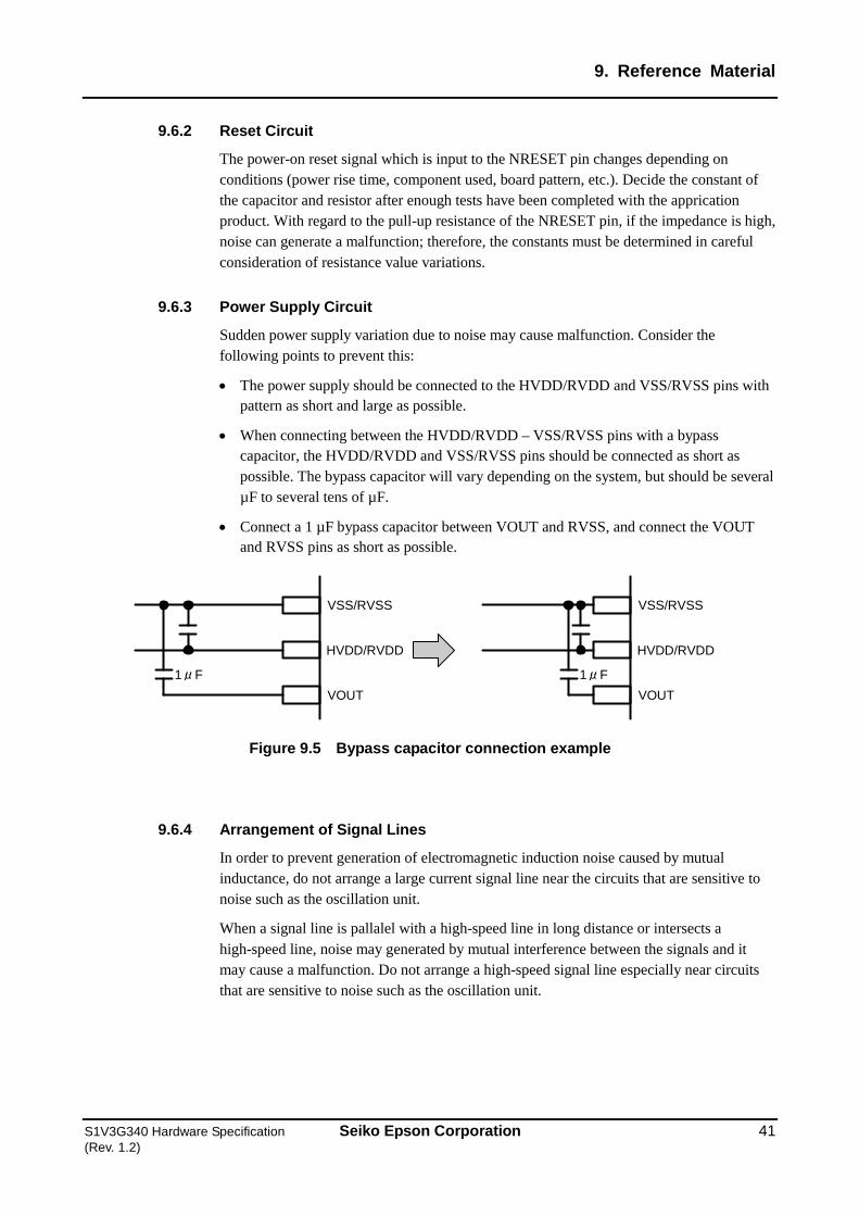
• When connecting between the HVDD/RVDD – VSS/RVSS pins with a bypass capacitor, the HVDD/RVDD and VSS/RVSS pins should be connected as short as possible. The bypass capacitor will vary depending on the system, but should be several µF to several tens of µF.
• Connect a 1 µF bypass capacitor between VOUT and RVSS, and connect the VOUT and RVSS pins as short as possible.
VSS/RVSS
HVDD/RVDD
VOUT1μF1μF
VSS/RVSS
HVDD/RVDD
VOUT
Figure 9.5 Bypass capacitor connection example
9.6.4 Arrangement of Signal Lines
In order to prevent generation of electromagnetic induction noise caused by mutual inductance, do not arrange a large current signal line near the circuits that are sensitive to noise such as the oscillation unit.
When a signal line is pallalel with a high-speed line in long distance or intersects a high-speed line, noise may generated by mutual interference between the signals and it may cause a malfunction. Do not arrange a high-speed signal line especially near circuits that are sensitive to noise such as the oscillation unit.
9. Reference Material
42 Seiko Epson Corporation S1V3G340 Hardware Specification (Rev. 1.2)
9.6.5 Noise-Induced Erratic Operations
If erratic IC operations appear to be attributable to noise, consider the following three points.
• NRESET pin Low-level noise on this pin resets the IC. However, the IC may not always be reset normally, depending on the input waveform. Due to circuit design, this situation tends to occur when the reset input is in the high state, with high impedance.
• SCKS pin The SCKS pin is a synchronous clock input of a clock synchronous serial interface. If a noise goes into this pin, depending on the input waveform, it will be recognized as valid data, and will become the cause of malfunction. When connecting between the host and serial interface (SCKS, SIS, SOS and NSCSS) pins, these should be connected as short as possible.
• Power supplies If noise lower than the rated voltage enters one of these power-supply lines, the IC may operate erratically. Take collective measures in board design; for example, by using soild patterns for power supply lines, adding decoupling capacitors to eliminate noise, or incorporating surge/noise counteracting devices into the power supply lines.
9.6.6 Others
Although the basic reliability of the S1V3G340 is designed to comply with EIAJ and MIL standards, please pay careful attention to the following points when actually mounting the chip on a board.
Since OSCI and OSCO pins are constructed to use the internal transistors directly, the pins are susceptible to mechanical damage during the board-mounting process. Moreover, the pins may also be susceptible to electraical damage caused by such disturbances (listed below) whose electrical strength are varying gradually with time and can exceed the absolute maximum rated voltage (2.5 V) of the IC.
• Electromagnetic induction noise from the utility power supply in the reflow process during board-mounting, rework process after board-mounting, or individual characteristics evaluation (experimental confirmation), and
• Electromagnetic induction noise fro the tip of a soldering iron
Especially when using a soldering iron, make sure that the IC GND and soldering iron GND are at the same potential before soldering.
9. Reference Material
S1V3G340 Hardware Specification Seiko Epson Corporation 43 (Rev. 1.2)
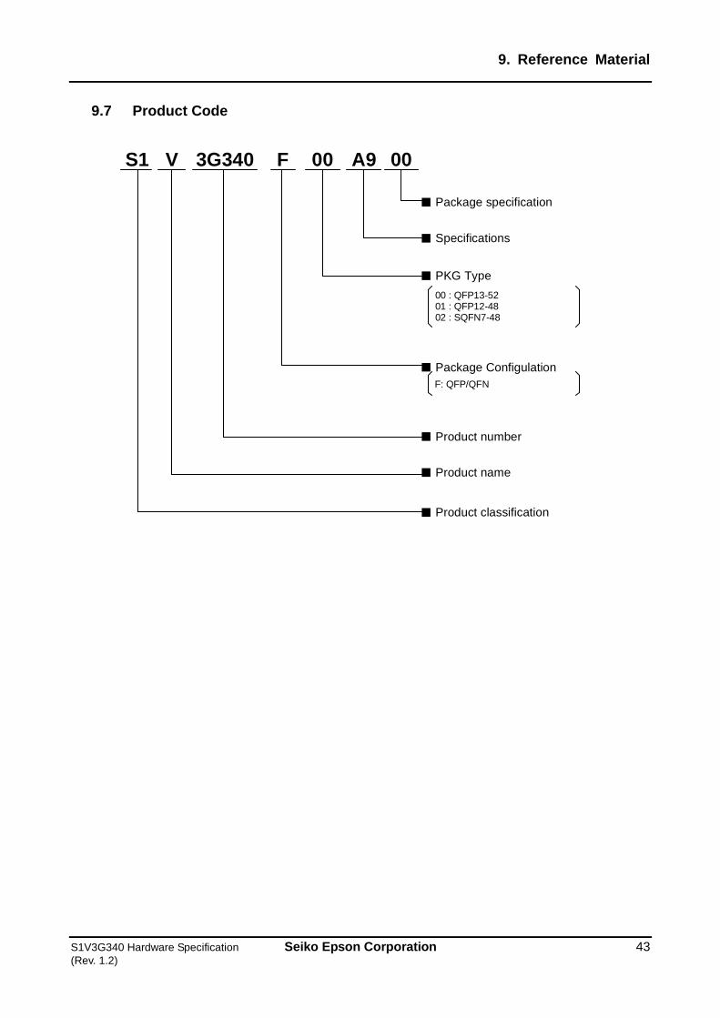
9.7 Product Code
S1 V 3G340 F A900 00
Package specification
Specifications
PKG Type00 : QFP13-5201 : QFP12-4802 : SQFN7-48
Package ConfigulationF: QFP/QFN
Product number
Product name
Product classification
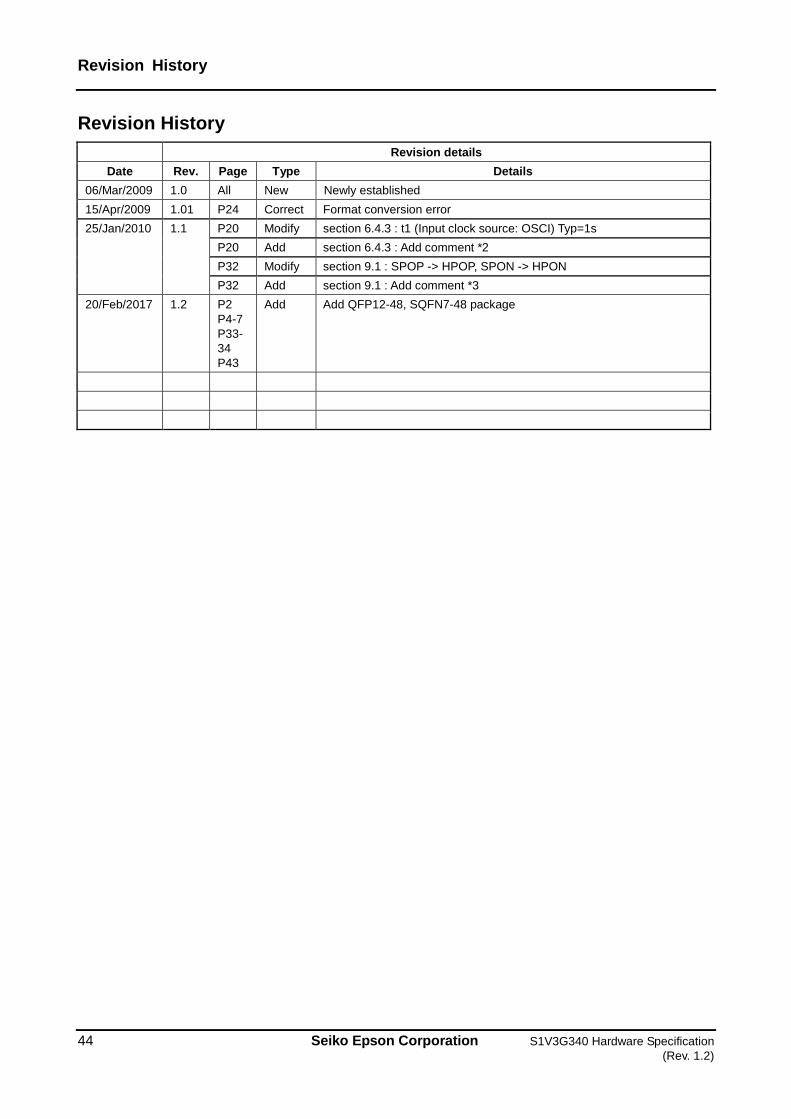
Revision History
44 Seiko Epson Corporation S1V3G340 Hardware Specification (Rev. 1.2)
Revision History Revision details
Date Rev. Page Type Details 06/Mar/2009 1.0 All New Newly established 15/Apr/2009 1.01 P24 Correct Format conversion error 25/Jan/2010 1.1 P20 Modify section 6.4.3 : t1 (Input clock source: OSCI) Typ=1s
P20 Add section 6.4.3 : Add comment *2 P32 Modify section 9.1 : SPOP -> HPOP, SPON -> HPON P32 Add section 9.1 : Add comment *3
20/Feb/2017 1.2 P2 P4-7 P33-34 P43
Add Add QFP12-48, SQFN7-48 package
International Sales Operations
AMERICA EPSON ELECTRONICS AMERICA, INC. 214 Devcon Drive, San Jose, CA 95112, USA Phone: +1-800-228-3964 FAX: +1-408-922-0238 EUROPE EPSON EUROPE ELECTRONICS GmbH Riesstrasse 15, 80992 Munich, GERMANY Phone: +49-89-14005-0 FAX: +49-89-14005-110
ASIA EPSON (CHINA) CO., LTD. 4th Floor, Tower 1 of China Central Place, 81 Jianguo Road, Chaoyang District, Beijing 100025 China Phone: +86-10-8522-1199 FAX: +86-10-8522-1120 SHANGHAI BRANCH Room 1701 & 1704, 17 Floor, Greenland Center II, 562 Dong An Road, Xu Hui District, Shanghai, CHINA Phone: +86-21-5330-4888 FAX: +86-21-5423-4677 SHENZHEN BRANCH Room 804-805, 8 Floor, Tower 2, Ali Center,No.3331 Keyuan South RD(Shenzhen bay), Nanshan District, Shenzhen 518054, CHINA Phone: +86-10-3299-0588 FAX: +86-10-3299-0560 EPSON TAIWAN TECHNOLOGY & TRADING LTD. 14F, No. 7, Song Ren Road, Taipei 110, TAIWAN Phone: +886-2-8786-6688 FAX: +886-2-8786-6660 EPSON SINGAPORE PTE., LTD. 1 HarbourFront Place, #03-02 HarbourFront Tower One, Singapore 098633 Phone: +65-6586-5500 FAX: +65-6271-3182 SEIKO EPSON CORP. KOREA OFFICE 19F, KLI 63 Bldg., 60 Yoido-dong, Youngdeungpo-Ku, Seoul 150-763, KOREA Phone: +82-2-784-6027 FAX: +82-2-767-3677 SEIKO EPSON CORP. MICRODEVICES OPERATIONS DIVISION Device Sales & Marketing Department 421-8, Hino, Hino-shi, Tokyo 191-8501, JAPAN
Phone: +81-42-587-5816 FAX: +81-42-587-5116
Document Code: 411696703 First Issue March 2009D
Revised March 2017 in JAPAN