s5u13706p00c100 evaluation board user manual - digi-key sheets/epson pdfs... · revision 1.1...
TRANSCRIPT

S1D13706 Embedded Memory LCD Controller
S5U13706P00C100 Evaluation Board User Manual
Document Number: X31B-G-021-01
Status: Revision 1.1
Issue Date: 2009/03/03
© SEIKO EPSON CORPORATION 2007 - 2009. All Rights Reserved.
Information in this document is subject to change without notice. You may download and use this document, but only for your own use inevaluating Seiko Epson/EPSON products. You may not modify the document. Epson Research and Development, Inc. disclaims anyrepresentation that the contents of this document are accurate or current. The Programs/Technologies described in this document may contain material protected under U.S. and/or International Patent laws.
EPSON is a registered trademark of Seiko Epson Corporation. All other Trademarks are the property of their respective owners
Revision 1.1
Page 2 Epson Research and DevelopmentVancouver Design Center
S1D13706 S5U13706P00C100 Evaluation Board User ManualX31B-G-021-01 Issue Date: 2009/03/03
Revision 1.1

Epson Research and Development Page 3Vancouver Design Center
Table of Contents
1 Introduction . . . . . . . . . . . . . . . . . . . . . . . . . . . . . . . . . . . . . . . . 5
2 Features . . . . . . . . . . . . . . . . . . . . . . . . . . . . . . . . . . . . . . . . . . 6
3 Installation and Configuration . . . . . . . . . . . . . . . . . . . . . . . . . . . . . . 73.1 Configuration DIP Switches . . . . . . . . . . . . . . . . . . . . . . . . . . 7
3.2 Configuration Jumpers . . . . . . . . . . . . . . . . . . . . . . . . . . . . 9
4 CPU Interface . . . . . . . . . . . . . . . . . . . . . . . . . . . . . . . . . . . . . . 114.1 CPU Interface Pin Mapping . . . . . . . . . . . . . . . . . . . . . . . . . 11
4.2 CPU Bus Connector Pin Mapping . . . . . . . . . . . . . . . . . . . . . . 12
5 LCD Interface Pin Mapping . . . . . . . . . . . . . . . . . . . . . . . . . . . . . . 14
6 Technical Description . . . . . . . . . . . . . . . . . . . . . . . . . . . . . . . . . 166.1 PCI Bus Support . . . . . . . . . . . . . . . . . . . . . . . . . . . . . 16
6.2 Direct Host Bus Interface Support . . . . . . . . . . . . . . . . . . . . . . 16
6.3 S1D13706 Embedded Memory . . . . . . . . . . . . . . . . . . . . . . . . 16
6.4 Software Adjustable LCD Backlight Intensity Support Using PWM . . . . . . . . . 16
6.5 Passive/Active LCD Panel Support . . . . . . . . . . . . . . . . . . . . . . 17
6.5.1 Buffered LCD Connector . . . . . . . . . . . . . . . . . . . . . . . . . . . . . . . 17
6.5.2 Extended LCD Connector . . . . . . . . . . . . . . . . . . . . . . . . . . . . . . . 17
6.6 External oscillator support for CLKI and CLKI2 . . . . . . . . . . . . . . . . . 17
7 References . . . . . . . . . . . . . . . . . . . . . . . . . . . . . . . . . . . . . . . 187.1 Documents . . . . . . . . . . . . . . . . . . . . . . . . . . . . . . . 18
7.2 Document Sources . . . . . . . . . . . . . . . . . . . . . . . . . . . . 18
8 Parts List . . . . . . . . . . . . . . . . . . . . . . . . . . . . . . . . . . . . . . . . 19
9 Schematics . . . . . . . . . . . . . . . . . . . . . . . . . . . . . . . . . . . . . . . 22
10 Board Layout . . . . . . . . . . . . . . . . . . . . . . . . . . . . . . . . . . . . . . 27
11 Technical Support . . . . . . . . . . . . . . . . . . . . . . . . . . . . . . . . . . . 2811.1 EPSON LCD Controllers (S1D13706) . . . . . . . . . . . . . . . . . . . . . 28
S5U13706P00C100 Evaluation Board User Manual S1D13706Issue Date: 2009/03/03 X31B-G-021-01
Revision 1.1

Page 4 Epson Research and DevelopmentVancouver Design Center
S1D13706 S5U13706P00C100 Evaluation Board User ManualX31B-G-021-01 Issue Date: 2009/03/03
Revision 1.1
Epson Research and Development Page 5Vancouver Design Center
1 Introduction
This manual describes the setup and operation of the S5U13706P00C100 Evaluation Board. The board is designed as an evaluation platform for the S1D13706 Embedded Memory LCD Controller.
This user manual is updated as appropriate. Please check the Epson Research and Devel-opment website at www.erd.epson.com for the latest revision of this document before beginning any development.
We appreciate your comments on our documentation. Please contact us via email at [email protected].
S5U13706P00C100 Evaluation Board User Manual S1D13706Issue Date: 2009/03/03 X31B-G-021-01
Revision 1.1
Page 6 Epson Research and DevelopmentVancouver Design Center
2 Features
Following are some features of the S5U13706P00C100 Evaluation Board:
• 100-pin TQFP S1D13706F00A Embedded Memory LCD Controller with 80K bytes of embedded SRAM.
• Headers for connecting to various Host Bus Interfaces.
• Configuration options.
• Software adjustable backlight intensity support.
• 4/8-bit 3.3V or 5V single monochrome passive LCD panel support.
• 4/8/16-bit 3.3V or 5V single color passive LCD panel support.
• 9/12/18-bit 3.3V or 5V active matrix TFT LCD panel support.
• Direct interface for 18-bit Epson D-TFD LCD panel support.
• Direct interface for 18-bit Sharp HR-TFT LCD panel support.
• Software initiated power save mode.
• Hardware or software Video Invert support.
• External oscillator for CLKI and CLKI2.
S1D13706 S5U13706P00C100 Evaluation Board User ManualX31B-G-021-01 Issue Date: 2009/03/03
Revision 1.1
Epson Research and Development Page 7Vancouver Design Center
3 Installation and Configuration
The S5U13706P00C100 is designed to support as many platforms as possible. The S5U13706P00C100 incorporates a DIP switch and three jumpers which allow both the evaluation board and S1D13706 LCD controller to be configured for a specified evaluation platform.
3.1 Configuration DIP Switches
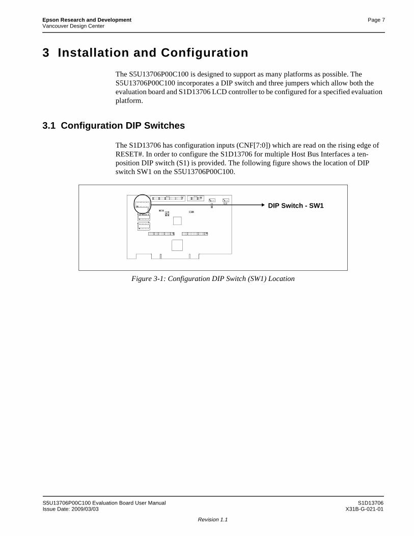
The S1D13706 has configuration inputs (CNF[7:0]) which are read on the rising edge of RESET#. In order to configure the S1D13706 for multiple Host Bus Interfaces a ten-position DIP switch (S1) is provided. The following figure shows the location of DIP switch SW1 on the S5U13706P00C100.
Figure 3-1: Configuration DIP Switch (SW1) Location
DIP Switch - SW1
S5U13706P00C100 Evaluation Board User Manual S1D13706Issue Date: 2009/03/03 X31B-G-021-01
Revision 1.1

Page 8 Epson Research and DevelopmentVancouver Design Center
The S1D13706 has 8 configuration inputs (CNF[7:0]) which are read on the rising edge of RESET#. All S1D13706 configuration inputs are fully configurable using a ten position DIP switch as described below.
Note1 To enable the Hardware Video Invert function the following are required:
• GPIO pins must be enabled (S1-4 closed).
• GPIO0 must be connected to S1-9 (Jumper JP1 set to 1-2).
• GPIO Pin Input Enable (REG[A9h] bit 7) must be set to 1b.
• GPIO0 Pin IO Configuration (REG[A8h] bit 0) must be set to 0b.
• Hardware Video Invert Enable bit (REG[70h] bit 5) must be set to 1b.
Table 3-1: Configuration DIP Switch Settings
SwitchS1D13706
SignalValue on this pin at rising edge of RESET# is used to configure:Closed (On/1) Open (Off/0)
SW1-[3:1] CNF[2:0]
Select host bus interface as follows:CNF2 CNF1 CNF0 Host Bus Interface
0 0 0 SH-4/SH-3
0 0 1 MC68K #10 1 0 MC68K #20 1 1 Generic #1
1 0 0 Generic #21 0 1 RedCap 21 1 0 DragonBall
1 1 1 ReservedNote: The host bus interface is 16-bit.
SW1-4 CNF3 Enable GPIO pins Enable additional pins for D-TFD/HR-TFT
SW1-5 CNF4 Big Endian bus interface Little Endian bus interfaceSW1-6 CNF5 WAIT# is active high WAIT# is active low
SW1-[8:7] CNF[7:6]
CLKI to BClk divide select:
CNF7 CNF6 CLKI to BClk Divide Ratio0 0 1 : 10 1 2 : 1
1 0 3 : 11 1 4 : 1
SW1-91 - Hardware Video Invert - invert video data1 Hardware Video Invert - normal video data1
SW1-10 - Disable FPGA for non-PCI host Enable FPGA for PCI host
= Required settings when used with PCI Bridge FPGA
S1D13706 S5U13706P00C100 Evaluation Board User ManualX31B-G-021-01 Issue Date: 2009/03/03
Revision 1.1

Epson Research and Development Page 9Vancouver Design Center
3.2 Configuration Jumpers
The S5U13706P00C100 has seven jumper blocks which configure various setting on the evaluation board. The jumper positions for each function are shown below.
JP1 - GPIO0 Connection
JP1 selects whether GPIO0 is connected to SW1-9. SW1-9 is used to enable hardware video invert on the S1D13706.When the jumper is on (position 1-2), SW1-9 controls the hardware video invert feature (default setting).When the jumper is off, the hardware video invert feature is disabled. This setting must be used for HR-TFT and D-TFD panels as GPIO0 is required for both panels. For details, refer to the S1D13706 Hardware Functional Specification, document number X31B-A-001-xx.
NoteWhen configured for Sharp HR-TFT or Epson D-TFD panels, JP1 must be set to no jumper and JP6 must be set to position 2-3.
Figure 3-2: Configuration Jumper (JP1) Location
Table 3-2: Jumper Summary
Jumper Function Position 1-2 Position 2-3 No Jumper
JP1 GPIO0 ConnectionGPIO0 connected to
SW1-9 for hardware video invert
—
GPIO0 disconnected from SW1-9 for direct
HR-TFT/D-TFD or GPIO testing
JP4 GP0 Polarity on H1 Normal (Active High) Inverted (Active Low) —JP6 LCD Panel Voltage +5V LCDVCC +3.3V LCDVCC —
= recommended settings
JP1
GPIO0 connected GPIO0 disconnectedto SW1-9 from SW1-9
S5U13706P00C100 Evaluation Board User Manual S1D13706Issue Date: 2009/03/03 X31B-G-021-01
Revision 1.1
Page 10 Epson Research and DevelopmentVancouver Design Center
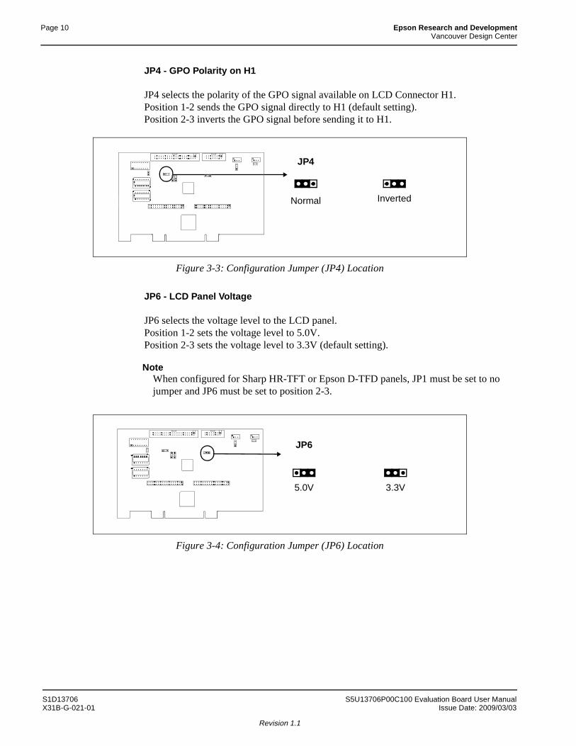
JP4 - GPO Polarity on H1
JP4 selects the polarity of the GPO signal available on LCD Connector H1.Position 1-2 sends the GPO signal directly to H1 (default setting).Position 2-3 inverts the GPO signal before sending it to H1.
Figure 3-3: Configuration Jumper (JP4) Location
JP6 - LCD Panel Voltage
JP6 selects the voltage level to the LCD panel.Position 1-2 sets the voltage level to 5.0V.Position 2-3 sets the voltage level to 3.3V (default setting).
NoteWhen configured for Sharp HR-TFT or Epson D-TFD panels, JP1 must be set to no jumper and JP6 must be set to position 2-3.
Figure 3-4: Configuration Jumper (JP6) Location
JP4
InvertedNormal
JP6
5.0V 3.3V
S1D13706 S5U13706P00C100 Evaluation Board User ManualX31B-G-021-01 Issue Date: 2009/03/03
Revision 1.1
Epson Research and Development Page 11Vancouver Design Center
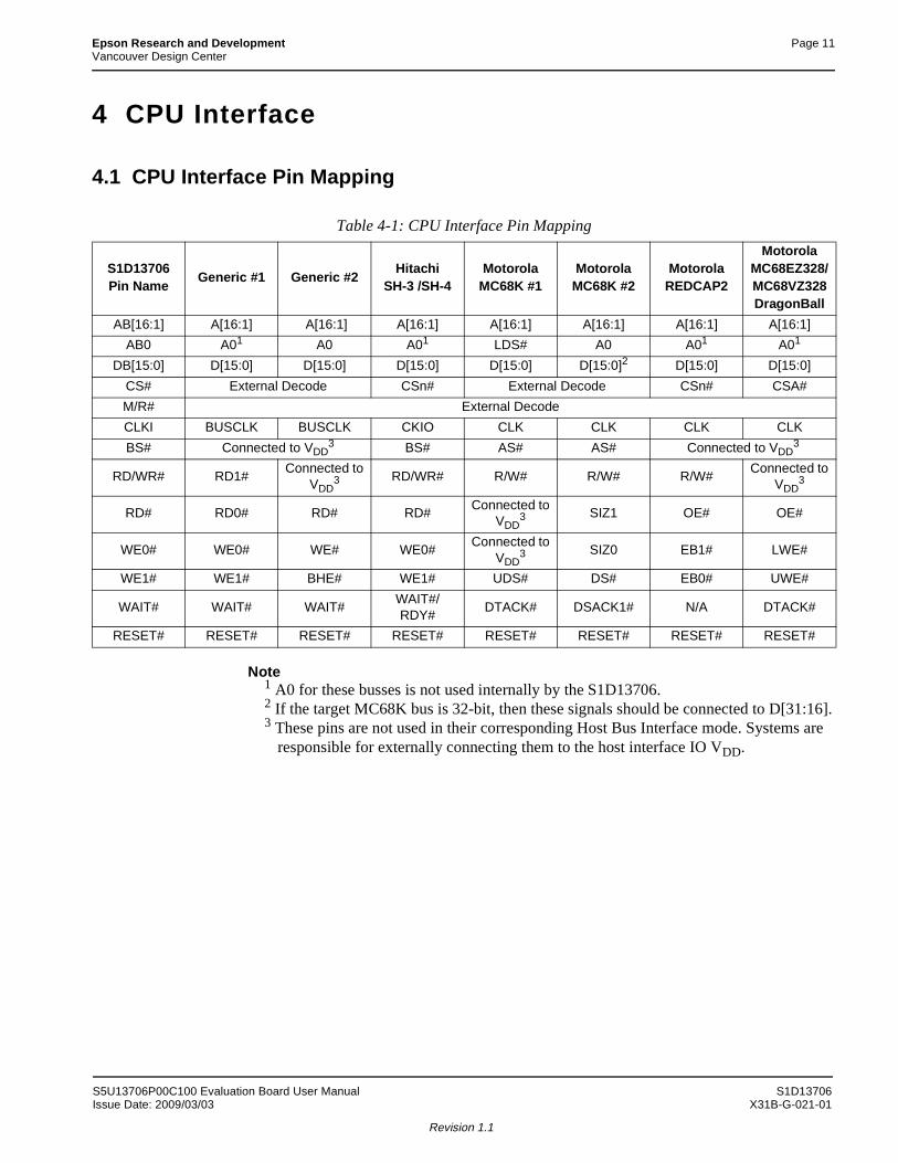
4 CPU Interface
4.1 CPU Interface Pin Mapping
Note1 A0 for these busses is not used internally by the S1D13706.2 If the target MC68K bus is 32-bit, then these signals should be connected to D[31:16].3 These pins are not used in their corresponding Host Bus Interface mode. Systems are
responsible for externally connecting them to the host interface IO VDD.
Table 4-1: CPU Interface Pin Mapping
S1D13706 Pin Name
Generic #1 Generic #2Hitachi
SH-3 /SH-4Motorola
MC68K #1Motorola
MC68K #2Motorola
REDCAP2
Motorola MC68EZ328/MC68VZ328 DragonBall
AB[16:1] A[16:1] A[16:1] A[16:1] A[16:1] A[16:1] A[16:1] A[16:1]
AB0 A01 A0 A01 LDS# A0 A01 A01
DB[15:0] D[15:0] D[15:0] D[15:0] D[15:0] D[15:0]2 D[15:0] D[15:0]
CS# External Decode CSn# External Decode CSn# CSA#
M/R# External Decode
CLKI BUSCLK BUSCLK CKIO CLK CLK CLK CLK
BS# Connected to VDD3 BS# AS# AS# Connected to VDD
3
RD/WR# RD1#Connected to
VDD3 RD/WR# R/W# R/W# R/W#
Connected to VDD
3
RD# RD0# RD# RD#Connected to
VDD3 SIZ1 OE# OE#
WE0# WE0# WE# WE0#Connected to
VDD3 SIZ0 EB1# LWE#
WE1# WE1# BHE# WE1# UDS# DS# EB0# UWE#
WAIT# WAIT# WAIT#WAIT#/RDY#
DTACK# DSACK1# N/A DTACK#
RESET# RESET# RESET# RESET# RESET# RESET# RESET# RESET#
S5U13706P00C100 Evaluation Board User Manual S1D13706Issue Date: 2009/03/03 X31B-G-021-01
Revision 1.1

Page 12 Epson Research and DevelopmentVancouver Design Center
4.2 CPU Bus Connector Pin Mapping
Table 4-2: CPU Bus Connector (H3) Pinout
Connector Pin No.
Comments
1 Connected to DB0 of the S1D13706
2 Connected to DB1 of the S1D13706
3 Connected to DB2 of the S1D13706
4 Connected to DB3 of the S1D13706
5 Ground
6 Ground
7 Connected to DB4 of the S1D13706
8 Connected to DB5 of the S1D13706
9 Connected to DB6 of the S1D13706
10 Connected to DB7 of the S1D13706
11 Ground
12 Ground
13 Connected to DB8 of the S1D13706
14 Connected to DB9 of the S1D13706
15 Connected to DB10 of the S1D13706
16 Connected to DB11 of the S1D13706
17 Ground
18 Ground
19 Connected to DB12 of the S1D13706
20 Connected to DB13 of the S1D13706
21 Connected to DB14 of the S1D13706
22 Connected to DB15 of the S1D13706
23 Connected to RESET# of the S1D13706
24 Ground
25 Ground
26 Ground
27 +12 volt supply
28 +12 volt supply
29 Connected to WE0# of the S1D13706
30 Connected to WAIT# of the S1D13706
31 Connected to CS# of the S1D13706
32 Connected to MR# of the S1D13706
33 Connected to WE1# of the S1D13706
34 Connected to TXVDD1
S1D13706 S5U13706P00C100 Evaluation Board User ManualX31B-G-021-01 Issue Date: 2009/03/03
Revision 1.1
Epson Research and Development Page 13Vancouver Design Center
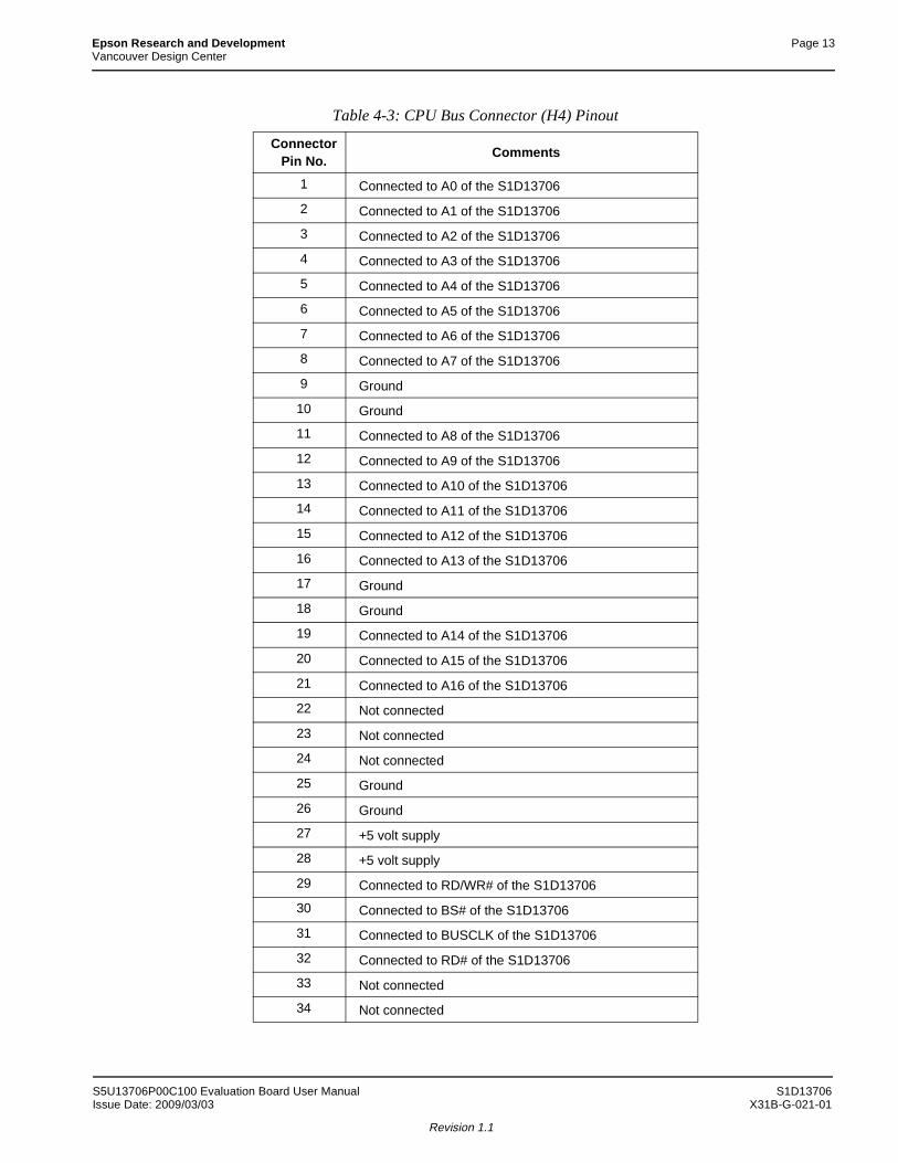
Table 4-3: CPU Bus Connector (H4) Pinout
Connector Pin No.
Comments
1 Connected to A0 of the S1D13706
2 Connected to A1 of the S1D13706
3 Connected to A2 of the S1D13706
4 Connected to A3 of the S1D13706
5 Connected to A4 of the S1D13706
6 Connected to A5 of the S1D13706
7 Connected to A6 of the S1D13706
8 Connected to A7 of the S1D13706
9 Ground
10 Ground
11 Connected to A8 of the S1D13706
12 Connected to A9 of the S1D13706
13 Connected to A10 of the S1D13706
14 Connected to A11 of the S1D13706
15 Connected to A12 of the S1D13706
16 Connected to A13 of the S1D13706
17 Ground
18 Ground
19 Connected to A14 of the S1D13706
20 Connected to A15 of the S1D13706
21 Connected to A16 of the S1D13706
22 Not connected
23 Not connected
24 Not connected
25 Ground
26 Ground
27 +5 volt supply
28 +5 volt supply
29 Connected to RD/WR# of the S1D13706
30 Connected to BS# of the S1D13706
31 Connected to BUSCLK of the S1D13706
32 Connected to RD# of the S1D13706
33 Not connected
34 Not connected
S5U13706P00C100 Evaluation Board User Manual S1D13706Issue Date: 2009/03/03 X31B-G-021-01
Revision 1.1
Page 14 Epson Research and DevelopmentVancouver Design Center
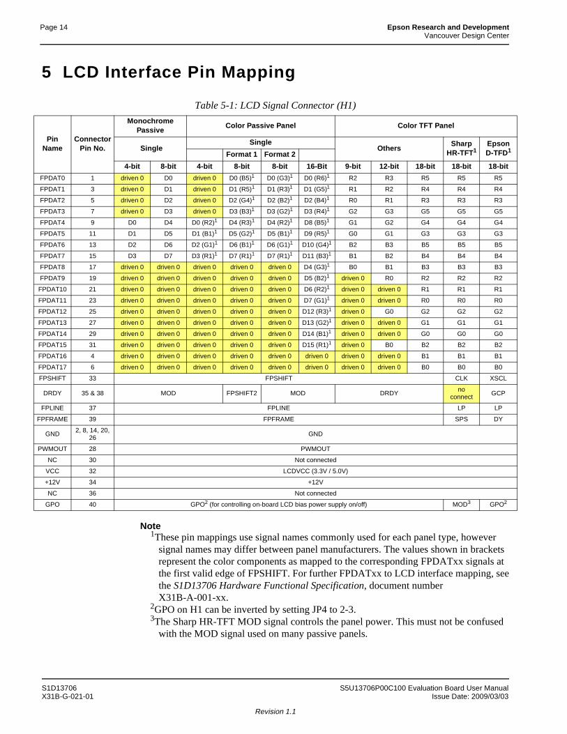
5 LCD Interface Pin Mapping
Note1These pin mappings use signal names commonly used for each panel type, however
signal names may differ between panel manufacturers. The values shown in bracketsrepresent the color components as mapped to the corresponding FPDATxx signals atthe first valid edge of FPSHIFT. For further FPDATxx to LCD interface mapping, seethe S1D13706 Hardware Functional Specification, document numberX31B-A-001-xx.
2GPO on H1 can be inverted by setting JP4 to 2-3.3The Sharp HR-TFT MOD signal controls the panel power. This must not be confused
with the MOD signal used on many passive panels.
Table 5-1: LCD Signal Connector (H1)
Pin Name
Connector Pin No.
Monochrome Passive
Color Passive Panel Color TFT Panel
SingleSingle
OthersSharp
HR-TFT1EpsonD-TFD1Format 1 Format 2
4-bit 8-bit 4-bit 8-bit 8-bit 16-Bit 9-bit 12-bit 18-bit 18-bit 18-bit
FPDAT0 1 driven 0 D0 driven 0 D0 (B5)1 D0 (G3)1 D0 (R6)1 R2 R3 R5 R5 R5
FPDAT1 3 driven 0 D1 driven 0 D1 (R5)1 D1 (R3)1 D1 (G5)1 R1 R2 R4 R4 R4
FPDAT2 5 driven 0 D2 driven 0 D2 (G4)1 D2 (B2)1 D2 (B4)1 R0 R1 R3 R3 R3
FPDAT3 7 driven 0 D3 driven 0 D3 (B3)1 D3 (G2)1 D3 (R4)1 G2 G3 G5 G5 G5
FPDAT4 9 D0 D4 D0 (R2)1 D4 (R3)1 D4 (R2)1 D8 (B5)1 G1 G2 G4 G4 G4
FPDAT5 11 D1 D5 D1 (B1)1 D5 (G2)1 D5 (B1)1 D9 (R5)1 G0 G1 G3 G3 G3
FPDAT6 13 D2 D6 D2 (G1)1 D6 (B1)1 D6 (G1)1 D10 (G4)1 B2 B3 B5 B5 B5
FPDAT7 15 D3 D7 D3 (R1)1 D7 (R1)1 D7 (R1)1 D11 (B3)1 B1 B2 B4 B4 B4
FPDAT8 17 driven 0 driven 0 driven 0 driven 0 driven 0 D4 (G3)1 B0 B1 B3 B3 B3
FPDAT9 19 driven 0 driven 0 driven 0 driven 0 driven 0 D5 (B2)1 driven 0 R0 R2 R2 R2
FPDAT10 21 driven 0 driven 0 driven 0 driven 0 driven 0 D6 (R2)1 driven 0 driven 0 R1 R1 R1
FPDAT11 23 driven 0 driven 0 driven 0 driven 0 driven 0 D7 (G1)1 driven 0 driven 0 R0 R0 R0
FPDAT12 25 driven 0 driven 0 driven 0 driven 0 driven 0 D12 (R3)1 driven 0 G0 G2 G2 G2
FPDAT13 27 driven 0 driven 0 driven 0 driven 0 driven 0 D13 (G2)1 driven 0 driven 0 G1 G1 G1
FPDAT14 29 driven 0 driven 0 driven 0 driven 0 driven 0 D14 (B1)1 driven 0 driven 0 G0 G0 G0
FPDAT15 31 driven 0 driven 0 driven 0 driven 0 driven 0 D15 (R1)1 driven 0 B0 B2 B2 B2
FPDAT16 4 driven 0 driven 0 driven 0 driven 0 driven 0 driven 0 driven 0 driven 0 B1 B1 B1
FPDAT17 6 driven 0 driven 0 driven 0 driven 0 driven 0 driven 0 driven 0 driven 0 B0 B0 B0
FPSHIFT 33 FPSHIFT CLK XSCL
DRDY 35 & 38 MOD FPSHIFT2 MOD DRDYno
connect GCP
FPLINE 37 FPLINE LP LP
FPFRAME 39 FPFRAME SPS DY
GND 2, 8, 14, 20, 26
GND
PWMOUT 28 PWMOUT
NC 30 Not connected
VCC 32 LCDVCC (3.3V / 5.0V)
+12V 34 +12V
NC 36 Not connected
GPO 40 GPO2 (for controlling on-board LCD bias power supply on/off) MOD3 GPO2
S1D13706 S5U13706P00C100 Evaluation Board User ManualX31B-G-021-01 Issue Date: 2009/03/03
Revision 1.1
Epson Research and Development Page 15Vancouver Design Center
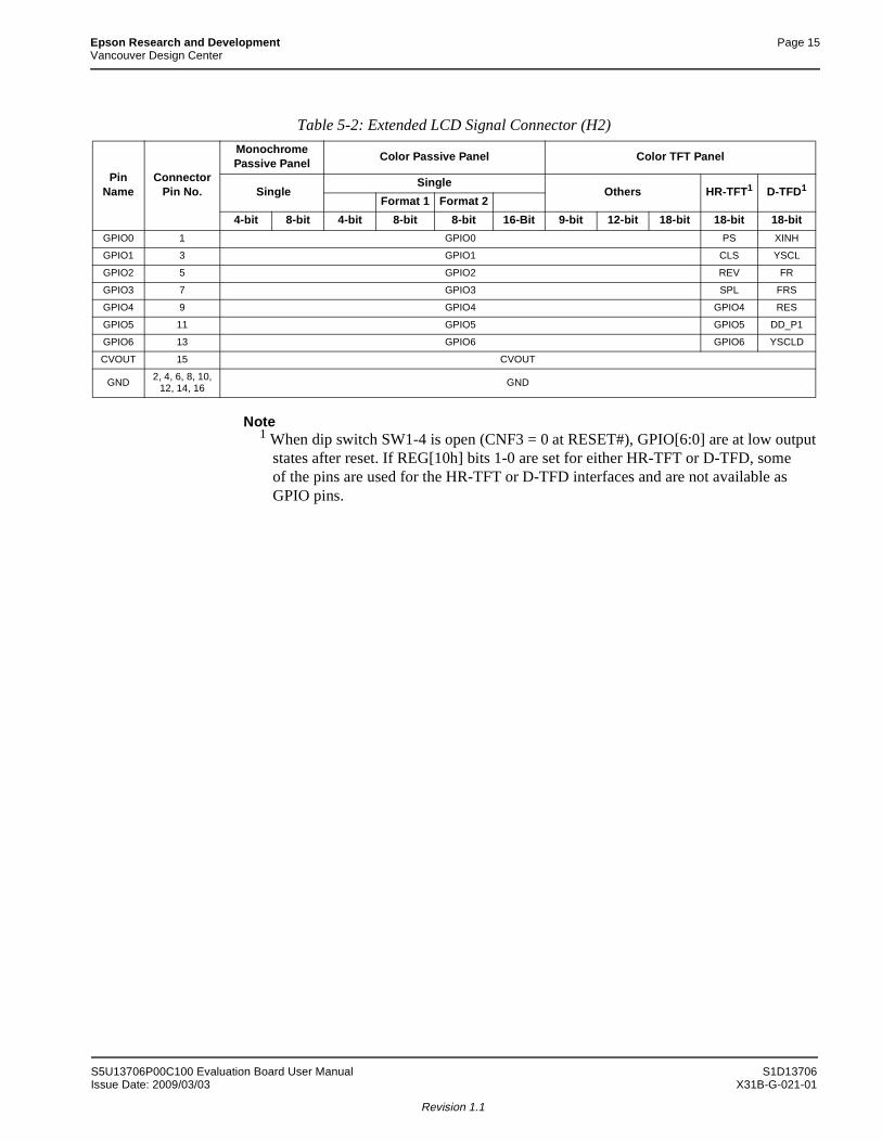
Note1 When dip switch SW1-4 is open (CNF3 = 0 at RESET#), GPIO[6:0] are at low output
states after reset. If REG[10h] bits 1-0 are set for either HR-TFT or D-TFD, someof the pins are used for the HR-TFT or D-TFD interfaces and are not available asGPIO pins.
Table 5-2: Extended LCD Signal Connector (H2)
Pin Name
Connector Pin No.
Monochrome Passive Panel
Color Passive Panel Color TFT Panel
SingleSingle
Others HR-TFT1 D-TFD1
Format 1 Format 2
4-bit 8-bit 4-bit 8-bit 8-bit 16-Bit 9-bit 12-bit 18-bit 18-bit 18-bit
GPIO0 1 GPIO0 PS XINH
GPIO1 3 GPIO1 CLS YSCL
GPIO2 5 GPIO2 REV FR
GPIO3 7 GPIO3 SPL FRS
GPIO4 9 GPIO4 GPIO4 RES
GPIO5 11 GPIO5 GPIO5 DD_P1
GPIO6 13 GPIO6 GPIO6 YSCLD
CVOUT 15 CVOUT
GND2, 4, 6, 8, 10,
12, 14, 16 GND
S5U13706P00C100 Evaluation Board User Manual S1D13706Issue Date: 2009/03/03 X31B-G-021-01
Revision 1.1

Page 16 Epson Research and DevelopmentVancouver Design Center
6 Technical Description
6.1 PCI Bus Support
The S1D13706 does not have on-chip PCI bus interface support. The S1D13706P00C100 uses the PCI Bridge FPGA to support the PCI bus.
6.2 Direct Host Bus Interface Support
The S5U13706P00C100 is specifically designed to work using the PCI Bridge FPGA in a standard PCI bus environment. However, the S1D13706 directly supports many other host bus interfaces. Connectors H3 and H4 provide the necessary IO pins to interface to these host buses. For further information on the host bus interfaces supported, see “CPU Interface” on page 11.
NoteThe PCI Bridge FPGA must be disabled using SW1-10 in order for direct host bus inter-faces to operate properly.
6.3 S1D13706 Embedded Memory
The S1D13706 has 80K bytes of embedded SRAM. The 80K byte display buffer address space is directly and contiguously available through the 17-bit address bus.
6.4 Software Adjustable LCD Backlight Intensity Support Using PWM
The S1D13706 provides Pulse Width Modulation output on PWMOUT. PWMOUT can be used to control LCD panels which support PWM control of the backlight inverter. The PWMOUT signal is provided on the buffered LCD connector (H1).
S1D13706 S5U13706P00C100 Evaluation Board User ManualX31B-G-021-01 Issue Date: 2009/03/03
Revision 1.1

Epson Research and Development Page 17Vancouver Design Center
6.5 Passive/Active LCD Panel Support
The S1D13706 directly supports:
• 4/8-bit single monochrome passive panels.
• 4/8/16-bit single color passive panels.
• 9/12/18-bit TFT active matrix panels.
• 18-bit Sharp HR-TFT panels.
• 18-bit Epson D-TFD panels.
All the necessary signals are provided on the 40-pin LCD connector, H1, and 16-pin Extended LCD Connector, H2. For connection information, see Section 5, “LCD Interface Pin Mapping” on page 14.
The S5U13706P00C100 does not provide a power supply for the LCD bias voltage needed by passive LCD panels. An external power supply is required to provide the bias LCD voltage to the LCD panel.
6.5.1 Buffered LCD Connector
The buffered LCD connector (H1) provides the same LCD panel signals as those directly from S1D13706, but with voltage-adapting buffers selectable to 3.3V or 5.0V. Pin 32 on this connector provides a voltage level of 3.3V or 5.0V to the LCD panel logic (see “JP6 - LCD Panel Voltage” on page 10 for information on setting the panel voltage).
6.5.2 Extended LCD Connector
The S1D13706 directly supports Sharp 18-bit HR-TFT and Epson 18-bit D-TFD panels. The extended LCD connector (H2) provides the extra signals required to support these panels. The signals on this connector are also buffered from the S1D13706 and adjustable to 3.3V or 5.0V (see “JP6 - LCD Panel Voltage” on page 10 for details on setting the panel voltage).
6.6 External oscillator support for CLKI and CLKI2
The S1D13706 uses CLKI and CLKI2 signals provided by two +5V oscillators. The oscil-lators are mounted on the evaluation board in 14-pin DIP sockets. The 5V clock signals are shifted to 3.3V which is accepted by the S1D13706.
S5U13706P00C100 Evaluation Board User Manual S1D13706Issue Date: 2009/03/03 X31B-G-021-01
Revision 1.1
Page 18 Epson Research and DevelopmentVancouver Design Center
7 References
7.1 Documents
• Epson Research and Development, Inc., S1D13706 Hardware Functional Specification, document number X31B-A-001-xx.
• Epson Research and Development, Inc., S1D13706 Programming Notes and Examples, document number X31B-G-003-xx.
7.2 Document Sources
• Epson Research and Development: http://www.erd.epson.com.
S1D13706 S5U13706P00C100 Evaluation Board User ManualX31B-G-021-01 Issue Date: 2009/03/03
Revision 1.1

Epson Research and Development Page 19Vancouver Design Center
8 Parts List
Table 8-1: Parts List
Item Qty Reference Part DescriptionManufacturer / Part No. / Assembly Instructions
1 16
C1, C2, C3, C4, C5, C6, C7, C8, C9, C10, C11, C13, C16, C17, C18, C19, C20, C21, C25,
C27, C29
0.1u50V X7R +/-5%, 1206
pckg.
Panasonic-ECG ECJ-3VB1H104K. Do not
populate C9, C10, C11, C25, C27
2 0 C26, C12 10u 10V 10u 10VDo not purchase. Do not
populate.
3 0 C15, C14 n/p 1206 pckg.Do not purchase. Do not
populate.
4 0 C22, C28 22u 10VTantalum C-Size, 10V +/-
10%Do not purchase. Do not
populate.
5 9C23, C38, C39, C40, C41, C42, C43, C44,
C45, C460.22uF
Ceramic Chip 0.22uF, 50V, X7R +/-5%, 1206
pckg
Kemet C1206C224J5RAC or equivalent capacitor
6 0 C24, C32 10u 63VElectrolytic, Radial Lead
63V +/-20%Do not purchase. Do not
populate.
7 4 C30, C34, C35, C37 68u 10VTantalum D-Size, 68uF,10V, +/-10%
Kemet T491D686K010AS (altern -Panasonic
ECST1AD686R (Digikey).
8 0 C31 1n50V X7R +/-5%, 1206
pckgDo not purchase. Do not
populate.
9 2 C36, C33 33u 20VTantalum D-Size, 33uF,20V, +/-10%
Kemet T491D336K020AS (altern -Panasonic
ECST1AD336R (Digikey)
10 0 D2, D1 1N5819Schottky Barrier Rectifier,
MELF pckg.Do not purchase. Do not
populate.
11 1 H1 HEADER 20X220x2, shrouded header,
keyed, straightSamtec TST-120-01-G-D
12 1 H2 HEADER 8X28x2, shrouded header,
keyed, straightSamtec TST-108-01-G-D
13 2 H4, H3 HEADER 17X217x2, 0.1” pitch, .025” sq.
unshrouded headerSamtec TSW-117-05-G-D
14 1 JP7, JP1 HEADER 22x1 .1” pitch unshrouded
headerDo not populate JP7
15 2JP2, JP3, JP4, JP5,
JP6HEADER 3
3x1 .1” pitch unshrouded header
Do not populate JP2, JP3, JP5
16 0 L2, L1 47uHShielded SMT power
inductor, +/-20%, 1.17A, 0.18 ohm
Do not purchase. Do not populate.
17 0 Q1 MMBT3906 PNP Transistor / SOT-23Do not purchase. Do not
populate.
S5U13706P00C100 Evaluation Board User Manual S1D13706Issue Date: 2009/03/03 X31B-G-021-01
Revision 1.1

Page 20 Epson Research and DevelopmentVancouver Design Center
18 0 Q2 MMFT3055VLN-channel FET, SOT-223
pckg.Do not purchase. Do not
populate.
19 0 Q3 FZT792AHigh gain transistor, SOT-
223 pckg.Do not purchase. Do not
populate.
20 0 Q4, Q5 MMBT2222ANPN transistor, SOT-23
pckg.Do not purchase. Do not
populate.
21 14R1-R9, R33, R36, R37,
R38, R3915K 1206 / 5%
22 9R10, R11, R12, R13, R14, R15, R16, R17,
R18330K 1206 / 5%
23 0 R19 12.4K 1% 1206 / 1%, E-96 seriesDo not purchase. Do not
populate.
24 0 R20, R21 80K 1206 / 5%Do not purchase. Do not
populate.
25 0 R22 402 1% 1206 / 1%, E-96 seriesDo not purchase. Do not
populate.
26 0 R23 301 1% 1206 / 1%, E-96 seriesDo not purchase. Do not
populate.
27 0 R24 200 POT Trim POTDo not purchase. Do not
populate.
28 0 R25 0.22 1/4W 1210 / 5% / 1/4WDo not purchase. Do not
populate.
29 0 R26 470 1206 / 5%Do not purchase. Do not
populate.
30 0 R27 22K 1206 / 5%Do not purchase. Do not
populate.
31 1 R28, R29, R32 100K 1206 / 5% Do not populate R28, R29
32 0 R30 1.2M 1206 / 5%Do not purchase. Do not
populate.
33 0 R31 500K POT Trim POTDo not purchase. Do not
populate.
34 3 R34, R35, R40, R41 1K 1206 / 5% Do not populate R41
35 1 SW1 SW DIP-10 Dip Switch 10-PositionGrayhill 76SB10ST
(Digikey GH1117-ND)
36 0 S1 SW DIP-4 DIP switch, 4-positionDo not purchase. Do not
populate.
37 1 U1 S1D13706F00A100-pin TQFP15 surface
mount package
38 0 U2 LT1117CST-55V fixed voltage regulator,
SOT-223Do not purchase. Do not
populate.
39 1 U3 74AHC04 SO-14 packageTI 74AHC04, SO-14
package
40 0 U4 ICD2061A Wide SO-16 packageDo not purchase. Do not
populate.
Table 8-1: Parts List
Item Qty Reference Part DescriptionManufacturer / Part No. / Assembly Instructions
S1D13706 S5U13706P00C100 Evaluation Board User ManualX31B-G-021-01 Issue Date: 2009/03/03
Revision 1.1

Epson Research and Development Page 21Vancouver Design Center
41 2 U6, U5 Test Socket14 pin narrow DIP, screw
machine socket
42 4 U7, U8, U9, U10 74HCT244 Buffer, SO-20 package TI74HCT244 or equivalent
43 0 U11 MAX754 16 pin narrow SO pckg.Do not purchase. Do not
populate.
44 1 U12 LT1117CM-3.33.3V fixed voltage
regulator, 3 Lead Plastic DD
Linear Technology LT1117CM-3.3
45 0 U13 MAX749 8 pin SO pckg.Do not purchase. Do not
populate.
46 1 U14 EPF6016TC144-2 144-pin QFP Altera EPF6016TC144-2
47 1 U15 8-pin DIP socket 8-pin DIP socket Machined socket, 8-pin
48 1 (U15) EPC1PI8N 8-pin DIP pckgAltera EPC1PI8N,
programmed, socketed
49 0 Y1 14.31818MHz Vertical-mount HC-49Do not purchase. Do not
populate.
50 3 (JP1), (JP4), (JP6) Micro Shunt
51 1 BracketComputer Bracket, Blank -
PCIKeystone - Cat. No. 9203
52 2 Screw Pan head, #4-40 x 1/4”Screw, pan head, #4-40 x
1/4”-please assemble bracket onto board
53 2Resistor SMD 0805
0ohm0 0805 Resistor, 0 ohm
please mount on solder side to short pins 2-3 of
JP2 and JP3
54 1 (U6) 50MHz Oscillator DIP14, 50MHzEpson SG8002DB, 50MHz, socketed
55 1 (U5) 6.5MHz Oscillator DIP14, 6.5MHzEpson SG8002DB, 6.5MHz, socketed
Table 8-1: Parts List
Item Qty Reference Part DescriptionManufacturer / Part No. / Assembly Instructions
S5U13706P00C100 Evaluation Board User Manual S1D13706Issue Date: 2009/03/03 X31B-G-021-01
Revision 1.1
Page 22 Epson Research and DevelopmentVancouver Design Center
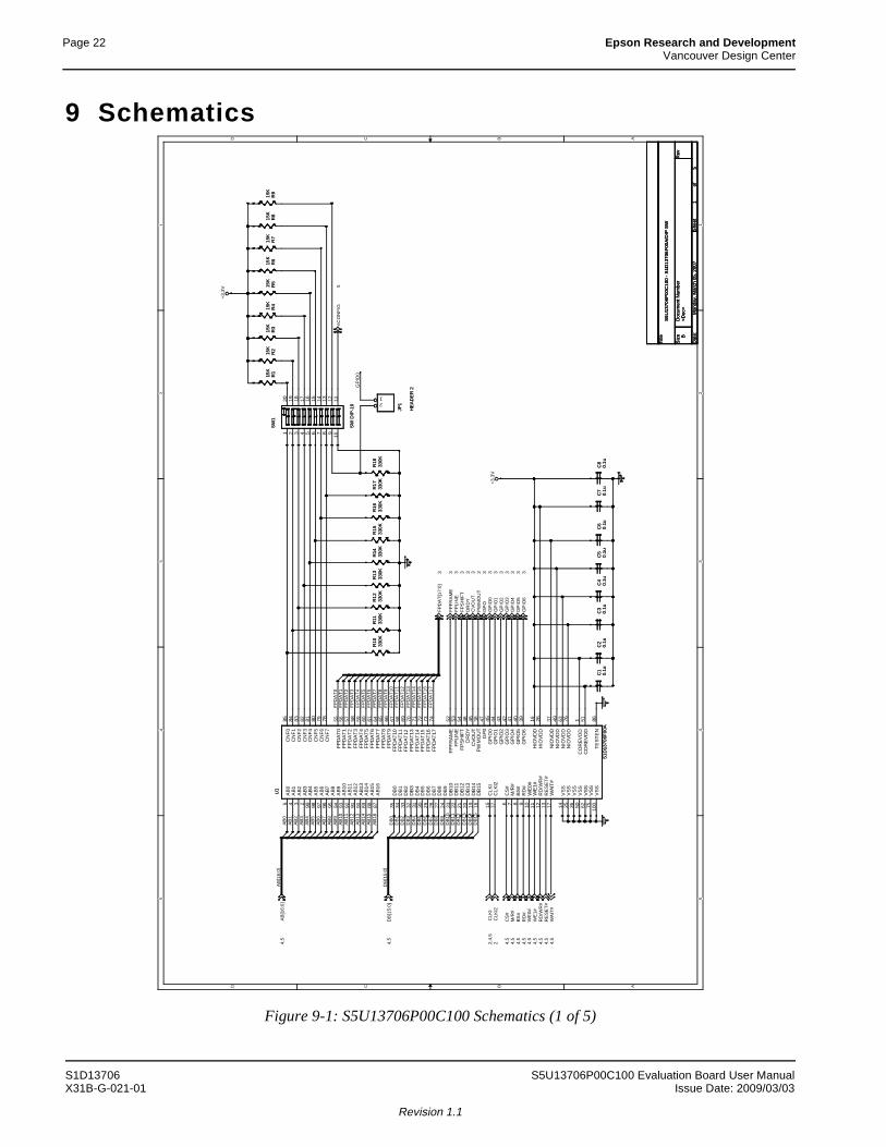
9 Schematics
Figure 9-1: S5U13706P00C100 Schematics (1 of 5)
5 5
4 4
3 3
2 2
1 1
DD
CC
BB
AA
DB
0D
B1
DB
2D
B3
DB
4D
B5
DB
6D
B7
DB
8D
B9
DB
10
DB
11
DB
12
DB
13
DB
14
DB
15
AB
[16:
0]
DB
[15
:0]
FP
DA
T1
3
FP
DA
T5
FP
DA
T8
FP
DA
T1
FP
DA
T0
FP
DA
T1
6
FP
DA
T1
4
FP
DA
T1
1
FP
DA
T1
7
FP
DA
T3
FP
DA
T7
FP
DA
T9
FP
DA
T4
FP
DA
T2
FP
DA
T1
0
FP
DA
T6
FP
DA
T1
2
FP
DA
T1
5
GP
IO0
AB
0A
B1
AB
2A
B3
AB
4A
B5
AB
6A
B7
AB
8A
B9
AB
10A
B11
AB
12A
B13
AB
14A
B15
AB
16
+3.
3V
+3.
3V
AB
[16:
0]
4,5
DB
[15:
0]4,
5
CLK
I22
CLK
I2,
4,5
WA
IT#
4,5
RD
/WR
#4,
5R
ES
ET
#4,
5
WE
1#4,
5W
E0#
4,5
RD
#4,
5B
S#
4,5
M/R
#4,
5C
S#
4,5
FP
DA
T[1
7:0
]3
FP
FR
AM
E3
FP
LIN
E3
FP
SH
IFT
3D
RD
Y3
CV
OU
T3
PW
MO
UT
3G
PO
3G
PIO
03
GP
IO1
3G
PIO
23
GP
IO3
3G
PIO
43
GP
IO5
3G
PIO
63
nCO
NF
IG5
Titl
e
Siz
eD
ocu
men
t Num
ber
Rev
Da
te:
She
eto
f
<D
oc>
S5
U13
706P
00C
100
- S
1D1
3706
F00
A/D
IP S
W
B
15
Mo
nday
, M
arch
05
, 200
7
Titl
e
Siz
eD
ocu
men
t Num
ber
Rev
Da
te:
She
eto
f
<D
oc>
S5
U13
706P
00C
100
- S
1D1
3706
F00
A/D
IP S
W
B
15
Mo
nday
, M
arch
05
, 200
7
Titl
e
Siz
eD
ocu
men
t Num
ber
Rev
Da
te:
She
eto
f
<D
oc>
S5
U13
706P
00C
100
- S
1D1
3706
F00
A/D
IP S
W
B
15
Mo
nday
, M
arch
05
, 200
7
R1
23
30K
R1
23
30K
R10
330K
R10
330K
R4
15K
R4
15K
R1
333
0KR
13
330K
U1
S1
D13
706F
00A
U1
S1
D13
706F
00A
AB
05
AB
14
AB
23
AB
32
AB
499
AB
598
AB
697
AB
796
AB
895
AB
994
AB
10
93
AB
11
92
AB
12
91
AB
13
90
AB
14
89
AB
15
88
AB
16
87
DB
035
DB
134
DB
233
DB
332
DB
431
DB
530
DB
629
DB
728
DB
827
DB
924
DB
1023
DB
1122
DB
1221
DB
1320
DB
1419
DB
1518
CL
KI
15
CL
KI2
77
CS
#6
M/R
#7
BS
#8
RD
#9
WE
0#
10
WE
1#
11
RD
/WR
#12
RE
SE
T#
13
WA
IT#
17
CN
F0
85
CN
F1
84
CN
F2
83
CN
F3
82
CN
F4
81
CN
F5
80
CN
F6
79
CN
F7
78
FP
DA
T0
55
FP
DA
T1
56
FP
DA
T2
57
FP
DA
T3
58
FP
DA
T4
59
FP
DA
T5
60
FP
DA
T6
61
FP
DA
T7
64
FP
DA
T8
65
FP
DA
T9
66
FP
DA
T10
67
FP
DA
T11
68
FP
DA
T12
69
FP
DA
T13
70
FP
DA
T14
71
FP
DA
T15
72
FP
DA
T16
73
FP
DA
T17
74
FP
FR
AM
E52
FP
LIN
E53
FP
SH
IFT
54
DR
DY
48
CV
OU
T46
PW
MO
UT
38
GP
047
GP
IO0
45
GP
IO1
44
GP
IO2
43
GP
IO3
42
GP
IO4
41
GP
IO5
40
GP
IO6
39
TE
ST
EN
86
VS
S14
VS
S25
VS
S36
VS
S50
VS
S62
VS
S75
VS
S10
0
HIO
VD
D16
HIO
VD
D26
NIO
VD
D37
NIO
VD
D49
NIO
VD
D63
NIO
VD
D76
CO
RE
VD
D1
CO
RE
VD
D51
R14
330K
R14
330K
C1
0.1u
C1
0.1u
C2
0.1
uC
20
.1u
R15
330
KR
153
30K
C3
0.1
uC
30
.1u
R1
63
30K
R1
63
30K
R9
15K
R9
15K
C4
0.1u
C4
0.1u
R1
733
0KR
17
330K
R6
15K
R6
15K
R18
330K
R18
330K
C5
0.1
uC
50
.1u
C6
0.1u
C6
0.1u
C7
0.1
uC
70.
1u
R7
15K
R7
15K
C8
0.1
uC
80
.1u
SW
1
SW
DIP
-10
SW
1
SW
DIP
-10
1 2 3 4 5 6 7 8 9
20 19 18 17 16 15 14 13 12 111
0
R3
15K
R3
15K
R5
15K
R5
15K
JP1
HE
AD
ER
2
JP1
HE
AD
ER
2
12
R2
15K
R2
15K
R8
15K
R8
15K
R1
15K
R1
15K
R11
330K
R11
330K
S1D13706 S5U13706P00C100 Evaluation Board User ManualX31B-G-021-01 Issue Date: 2009/03/03
Revision 1.1

Epson Research and Development Page 23Vancouver Design Center
Figure 9-2: S5U13706P00C100 Schematics (2 of 5)
5 5
4 4
3 3
2 2
1 1
DD
CC
BB
AA
+5V
+5V
+3.3
V
+3.3
V
+3.3
V
+3.3
V
+3.3
V
+3.3
V
+3.3
V
+5V
+5V
LCD
VC
C
CLK
I1,
4,5
CLK
I21
BU
SC
LK1,
4,5
Title
Siz
eD
ocum
ent N
umbe
rR
ev
Dat
e:S
heet
of
<Doc
>
S5U
1370
6P00
C10
0 - C
lock
s an
d P
ower
Sup
plie
s
B
25
Mon
day,
Mar
ch 0
5, 2
007
Title
Siz
eD
ocum
ent N
umbe
rR
ev
Dat
e:S
heet
of
<Doc
>
S5U
1370
6P00
C10
0 - C
lock
s an
d P
ower
Sup
plie
s
B
25
Mon
day,
Mar
ch 0
5, 2
007
Title
Siz
eD
ocum
ent N
umbe
rR
ev
Dat
e:S
heet
of
<Doc
>
S5U
1370
6P00
C10
0 - C
lock
s an
d P
ower
Sup
plie
s
B
25
Mon
day,
Mar
ch 0
5, 2
007
For U
3
1 2
5
.0V
LC
D P
anel
s2
3
3.3
V L
CD
Pan
els
U12
LT11
17C
M-3
.3U
12LT
1117
CM
-3.3
VIN
3
ADJ 1
VO
UT
2
JP6
HE
AD
ER
3JP
6H
EA
DE
R 3
123
U6
Test
Soc
ket
U6
Test
Soc
ket
NC
1
OU
T8
GN
D7
VCC
14
U3F
74A
HC
04
U3F
74A
HC
04
1312
14 7
C16
0.1u
C16
0.1u
U5
Test
Soc
ket
U5
Test
Soc
ket
NC
1
OU
T8
GN
D7
VCC
14
C17
0.1u
C17
0.1u
C13
0.1u
C13
0.1u
C29
0.1u
C29
0.1u
+C
3068
u 10
V+
C30
68u
10V
U3B
74A
HC
04
U3B
74A
HC
04
34
14 7
U3C
74A
HC
04
U3C
74A
HC
04
56
14 7
U3D
74A
HC
04
U3D
74A
HC
04
98
14 7
U3A
74A
HC
04
U3A
74A
HC
04
12
14 7
S5U13706P00C100 Evaluation Board User Manual S1D13706Issue Date: 2009/03/03 X31B-G-021-01
Revision 1.1
Page 24 Epson Research and DevelopmentVancouver Design Center
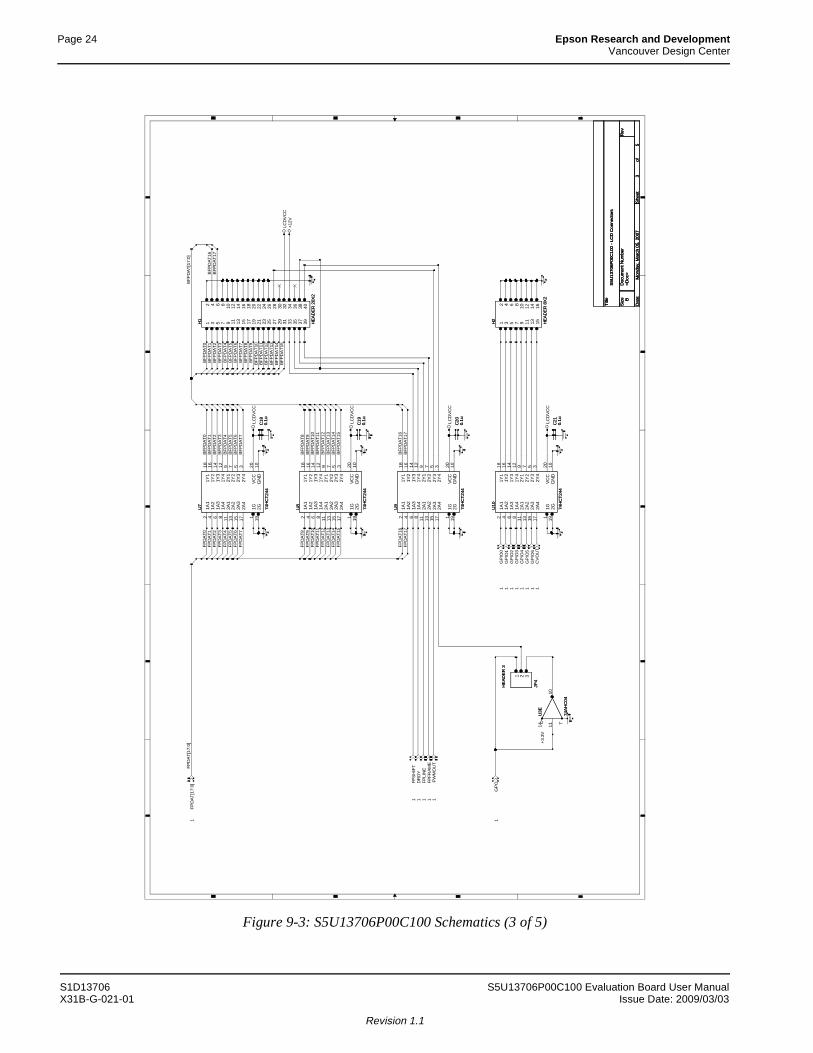
Figure 9-3: S5U13706P00C100 Schematics (3 of 5)
5 5
4 4
3 3
2 2
1 1
DD
CC
BB
AA
FPD
AT6
FPD
AT0
FPD
AT1
FPD
AT5
FPD
AT4
FPD
AT2
FPD
AT7
FPD
AT3
FPD
AT1
4FP
DA
T13
FPD
AT1
5
FPD
AT1
1FP
DA
T12
FPD
AT9
FPD
AT8
FPD
AT1
0
FPD
AT1
6FP
DA
T17
BFP
DA
T[17
:0]
FPD
AT[
17:0
]
BFP
DA
T12
BFP
DA
T5
BFP
DA
T15
BFP
DA
T12
BFP
DA
T10
BFP
DA
T3
BFP
DA
T6
BFP
DA
T0
BFP
DA
T15
BFP
DA
T9
BFP
DA
T5
BFP
DA
T10
BFP
DA
T14
BFP
DA
T11
BFP
DA
T7
BFP
DA
T1B
FPD
AT0
BFP
DA
T2
BFP
DA
T17
BFP
DA
T6
BFP
DA
T14
BFP
DA
T11
BFP
DA
T8
BFP
DA
T4
BFP
DA
T7
BFP
DA
T16
BFP
DA
T2
BFP
DA
T13
BFP
DA
T8
BFP
DA
T1
BFP
DA
T9
BFP
DA
T13
BFP
DA
T3B
FPD
AT4
BFP
DA
T16
BFP
DA
T17
LCD
VC
C
LCD
VC
C
LCD
VC
C
+12V
LCD
VC
C
LCD
VC
C+3
.3V
FPD
AT[
17:0
]1
GP
IO3
1
CV
OU
T1
GP
IO4
1G
PIO
51
GP
IO2
1G
PIO
11
GP
IO6
1
GP
IO0
1G
PO
1
PW
MO
UT
1
FPS
HIF
T1
DR
DY
1
FPFR
AM
E1
FPLI
NE
1
Title
Siz
eD
ocum
ent N
umbe
rR
ev
Dat
e:S
heet
of
<Doc
>
S5U
1370
6P00
C10
0 - L
CD
Con
nect
ors
B
35
Mon
day,
Mar
ch 0
5, 2
007
Title
Siz
eD
ocum
ent N
umbe
rR
ev
Dat
e:S
heet
of
<Doc
>
S5U
1370
6P00
C10
0 - L
CD
Con
nect
ors
B
35
Mon
day,
Mar
ch 0
5, 2
007
Title
Siz
eD
ocum
ent N
umbe
rR
ev
Dat
e:S
heet
of
<Doc
>
S5U
1370
6P00
C10
0 - L
CD
Con
nect
ors
B
35
Mon
day,
Mar
ch 0
5, 2
007
C19
0.1u
C19
0.1u
H1
HE
AD
ER
20X
2
H1
HE
AD
ER
20X
2
12
34
56
78
910
1112
1314
1516
1718
1920
2122
2324
2526
2728
2930
3132
3334
3536
3738
3940
U7
74H
CT2
44
U7
74H
CT2
44
1A1
21A
24
1A3
6
1A4
8
2A1
112A
213
2A3
152A
417
1G1
2G19
1Y1
181Y
216
1Y3
14
1Y4
12
2Y1
92Y
27
2Y3
52Y
43
VCC
20G
ND
10
U9
74H
CT2
44
U9
74H
CT2
44
1A1
21A
24
1A3
61A
48
2A1
11
2A2
13
2A3
152A
417
1G1
2G19
1Y1
181Y
216
1Y3
141Y
412
2Y1
9
2Y2
7
2Y3
52Y
43
VCC
20G
ND
10
C18
0.1u
C18
0.1u
JP4
HE
AD
ER
3
JP4
HE
AD
ER
3
1 2 3
U10
74H
CT2
44
U10
74H
CT2
44
1A1
21A
24
1A3
61A
48
2A1
11
2A2
13
2A3
15
2A4
17
1G1
2G19
1Y1
181Y
216
1Y3
141Y
412
2Y1
9
2Y2
7
2Y3
5
2Y4
3
VCC
20G
ND
10
U8
74H
CT2
44
U8
74H
CT2
44
1A1
21A
24
1A3
6
1A4
8
2A1
11
2A2
132A
315
2A4
17
1G1
2G19
1Y1
181Y
216
1Y3
14
1Y4
12
2Y1
9
2Y2
72Y
35
2Y4
3
VCC
20G
ND
10
H2
HE
AD
ER
8X
2
H2
HE
AD
ER
8X
2
12
34
56
78
910
1112
1314
1516
C20
0.1u
C20
0.1u
U3E
74A
HC
04
U3E
74A
HC
04
1110
14 7C
210.
1uC
210.
1u
S1D13706 S5U13706P00C100 Evaluation Board User ManualX31B-G-021-01 Issue Date: 2009/03/03
Revision 1.1
Epson Research and Development Page 25Vancouver Design Center
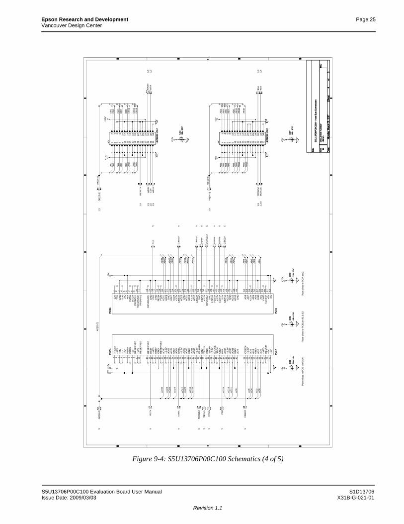
Figure 9-4: S5U13706P00C100 Schematics (4 of 5)
5 5
4 4
3 3
2 2
1 1
DD
CC
BB
AA
AB
[16:
0]
DB
5
DB
[15:
0]
DB
8
DB
4
DB
12
DB
3
DB
11
DB
2
DB
13
DB
1
DB
10
DB
0
DB
9
DB
14
DB
6D
B7
DB
15
AB
0A
B2
AB
4A
B6
AB
8A
B10
AB
12
AB
14A
B16
AB
5A
B7
AB
1A
B3
AB
11A
B9
AB
13
AB
15
AD
27A
D28
AD
21
AD
3
AD
9
AD
6
AD
22
AD
15
AD
13
AD
4
AD
1
AD
23
AD
10
AD
25
AD
11
AD
20
AD
7
AD
0
AD
8
AD
16A
D18
AD
[31:
0]
AD
30
AD
2
AD
5
AD
12
AD
31A
D29
AD
14
AD
17
AD
24
AD
19
AD
26
+5V
+5V
+12V
+12V
+12V
+5V
+5V
+5V
+12V
+12V
+5V
+5V
AB
[16:
0]1,
5
RD
/WR
#1,
5B
US
CLK
1,2,
5B
S#
1,5
RD
#1,
5
WE
0#1,
5
WE
1#1,
5C
S#
1,5
M/R
#1,
5W
AIT
#1,
5
RE
SE
T#1,
5
DB
[15:
0]1,
5
STO
P#
5
PA
R5
SE
RR
#5
IDS
EL
5
RS
T#5
C/B
E0#
5
C/B
E1#
5
DE
VS
EL#
5
CLK
5
C/B
E2#
5
TRD
Y#
5
FRA
ME
#5
AD
[31:
0]5
C/B
E3#
5
IRD
Y#
5
PE
RR
#5
Title
Siz
eD
ocum
ent N
umbe
rR
ev
Dat
e:S
heet
of
<Doc
>
S5U
1370
6P00
C10
0 - H
ost B
us C
onne
ctor
s
B
45
Mon
day,
Mar
ch 0
5, 2
007
Title
Siz
eD
ocum
ent N
umbe
rR
ev
Dat
e:S
heet
of
<Doc
>
S5U
1370
6P00
C10
0 - H
ost B
us C
onne
ctor
s
B
45
Mon
day,
Mar
ch 0
5, 2
007
Title
Siz
eD
ocum
ent N
umbe
rR
ev
Dat
e:S
heet
of
<Doc
>
S5U
1370
6P00
C10
0 - H
ost B
us C
onne
ctor
s
B
45
Mon
day,
Mar
ch 0
5, 2
007
Pla
ce c
lose
to P
CIB
pin
61
& 6
2P
lace
clo
se to
PC
IA p
in 2
Pla
ce c
lose
to P
CIB
pin
5 &
6
+C
3633
u 20
V+
C36
33u
20V
PC
IB1
PC
I-B
PC
IB1
PC
I-B
-12V
1TC
K2
GN
D3
TDO
4
+5V
5+5
V6
INTB
#7
INTD
#8
PR
SNT#
19
RES
ERV
ED10
PR
SNT#
211
RES
ERV
ED14
GN
D15
CLK
16G
ND
17
RE
Q#
18+V
I/O19
AD31
20AD
2921
GN
D22
AD27
23
AD25
24
+3.3
V25
C/B
E3#
26AD
2327
GN
D28
AD21
29AD
1930
+3.3
V31
AD17
32
C/B
E2#
33
GN
D34
IRD
Y#
35+3
.3V
36D
EVS
EL#
37G
ND
38LO
CK
#39
PER
R#
40+3
.3V
41S
ERR
#42
3.3V
43
C/B
E1#
44
AD14
45G
ND
46
AD12
47AD
1048
GN
D49
AD
852
AD
753
+3.3
V54
AD
555
AD
356
GN
D57
AD
158
+VI/O
59A
CK6
4#60
+5V
61+5
V62
PC
IA1
PC
I-A
PC
IA1
PC
I-A
TRST
#1
+12V
2
TMS
3
TDI
4
+5V
5IN
TA#
6IN
TC#
7+5
V8
RE
SER
VED
9+V
I/O10
RE
SER
VED
11
RE
SER
VED
14
RS
T#15
+VI/O
16G
NT#
17
GN
D18
RE
SER
VED
19AD
3020
+3.3
V21
AD28
22
AD26
23
GN
D24
AD24
25ID
SEL
26+3
.3V
27AD
2228
AD20
29G
ND
30AD
1831
AD16
32
+3.3
V33
FRAM
E#34
GN
D35
TRD
Y#
36G
ND
37ST
OP
#38
+3.3
V39
SDO
NE
40SB
O#
41G
ND
42
PAR
43
AD15
44
+3.3
V45
AD13
46
AD11
47G
ND
48AD
949
C/B
E0#
52
+3.3
V53
AD6
54
AD4
55G
ND
56AD
257
AD0
58+V
I/O59
RE
Q64
#60
+5V
61+5
V62
+C
3333
u 20
V+
C33
33u
20V
+C
3468
u 10
V+
C34
68u
10V
+C
3568
u 10
V+
C35
68u
10V
H4
HE
AD
ER
17X
2
H4
HE
AD
ER
17X
2
12
34
56
78
910
1112
1314
1516
1718
1920
2122
2324
2526
2728
2930
3132
3334
H3
HE
AD
ER
17X
2
H3
HE
AD
ER
17X
2
12
34
56
78
910
1112
1314
1516
1718
1920
2122
2324
2526
2728
2930
3132
3334
+C
3768
u 10
V+
C37
68u
10V
S5U13706P00C100 Evaluation Board User Manual S1D13706Issue Date: 2009/03/03 X31B-G-021-01
Revision 1.1

Page 26 Epson Research and DevelopmentVancouver Design Center
Figure 9-5: S5U13706P00C100 Schematics (5 of 5)
A A
B B
C C
D D
E E
44
33
22
11
AD13
AD9
AD15
AD16
AD18
AD23
AD10
AD12
AD19
AD24
AD8
AD20
AD22
AD25
AD17
AD11
AD21
AD14
AD
0A
D1
AD
2A
D3
AD
4
AD
5A
D6
AD
7A
D27
AD
26
AD
29
AD
28
AD
30A
D31
DB15DB14
DB13DB12
DB11DB10
DB
9
DB
2D
B1
DB
0
DB
6D
B5
DB
3D
B4
DB
7D
B8
AB
15A
B16
AB9
AB
[16:
0]
AB1AB0
AB11
AB2
AB12
AB4
AB10
AB6
AB13
AB8
AB5
AB7
AB
14
AB3
DCLK
DATA nSTATUS
CO
NF_
DO
NE
nSTA
TUS
CO
NF_
DO
NE
DC
LKD
ATA
AD
[31:
0]
DB
[15:
0]+5
V
+5V
+5V
+5V
+5V
+5V
+5V
+5V
+5V
+5V
+5V
+5V
+5V
+5V
+5V
+3.3
V
+3.3
V+3
.3V
+3.3
V+3
.3V
+3.3
V
TRD
Y#
4
STO
P#
4
PA
R4
IRD
Y#
4
DE
VS
EL#
4
PE
RR
#4
SE
RR
#4
AB
[16:
0]1,
4
M/R
#1,
4
WE
0#1,
4
DB
[15:
0]1,
4
BS
#1,
4R
D#
1,4
WE
1#1,
4R
D/W
R#
1,4
CS
#1,
4
BU
SC
LK1,
2,4
RE
SE
T#1,
4
C/B
E0#
4
IDS
EL
4C
/BE
3#4
C/B
E1#
4
WA
IT#
1,4
FRA
ME
#4
C/B
E2#
4
AD
[31:
0]4
RS
T#4
CLK
4
nCO
NFI
G1
Title
Siz
eD
ocum
ent N
umbe
rR
ev
Dat
e:S
heet
of
<Doc
>
S5U
1370
6P00
C10
0 - F
PG
A--
6016
B
55
Mon
day,
Mar
ch 0
5, 2
007
Title
Siz
eD
ocum
ent N
umbe
rR
ev
Dat
e:S
heet
of
<Doc
>
S5U
1370
6P00
C10
0 - F
PG
A--
6016
B
55
Mon
day,
Mar
ch 0
5, 2
007
Title
Siz
eD
ocum
ent N
umbe
rR
ev
Dat
e:S
heet
of
<Doc
>
S5U
1370
6P00
C10
0 - F
PG
A--
6016
B
55
Mon
day,
Mar
ch 0
5, 2
007
FPG
A c
onfig
urat
ion
EPR
OM
Not
Pop
ulat
ed
U14
EP
F601
6TC
144-
2U
14E
PF6
016T
C14
4-2
IO1
1IO
22
IO3
3nC
E4
GN
D5
Vcc
int
6
Vcc
io7
IO8
8IO
99
IO10
10IO
1111
IO12
12IO
1313
IO14
14IO
1515
IO16
16
I17
17
GN
D18
Vcc
io19
I20
20IO
2121
IO22
22IO
2323
IO24
24IO
2525
IO26
26
IO27
27
IO28
28IO
2929
GN
D30
Vcc
int
31V
ccio
32M
SEL
33IO
3434
IO35
35
IO36
36
IO37 37
IO38 38
IO39 39IO40 40IO41 41IO42 42IO43 43IO44 44IO45 45IO46 46
IO47 47
IO48 48
IO49 49IO50 50IO51 51IO52 52nCONFIG 53GND 54Vccio 55nSTATUS 56
IO57 57
IO58 58
IO59 59IO60 60IO61 61IO62 62IO63 63IO64 64IO65 65IO66 66
IO67 67
IO68 68
IO69 69IO70 70IO71 71IO72 72IO
7373
IO74
74IO
7575
GN
D76
Vcc
int
77V
ccio
78IO
7979
IO80
80IO
8181
IO82
82IO
8383
IO84
84IO
8585
IO86
86IO
8787
IO88
88I8
989
GN
D90
Vcc
io91
I92
92IO
9393
IO94
94IO
9595
IO96
96IO
9797
IO98
98IO
9999
IO10
010
0IO
101
101
GN
D10
2V
ccin
t10
3V
ccio
104
CO
NF_
DO
NE
105
IO10
610
6IO
107
107
IO10
810
8
IO109109 IO110110 IO111111 IO112112 IO113113 IO114114 IO115115 IO116116 IO117117 IO118118 IO119119 IO120120 IO121121 IO122122 IO123123 IO124124 DATA125 GND126 Vccio127 DCLK128 IO129129 IO130130 IO131131 IO132132 IO133133 IO134134 IO135135 IO136136 IO137137 IO138138 IO139139 IO140140 IO141141 IO142142 IO143143 IO144144C
380.
22u
C38
0.22
u
R36
15K
R36
15K
R37
15K
R37
15K
R38
15K
R38
15K
R39
15K
R39
15K
R33
15K
R33
15K
U15 EP
C14
41P
C8
U15 EP
C14
41P
C8
DAT
A1
DC
LK2
OE
3nC
S4
GN
D5
nCAS
C6
VCC
7VC
C8
R34
1KR34
1KR
351KR
351K
R40
1KR40
1K
S1
SW
DIP
-4
S1
SW
DIP
-4
1 2 3 4
8 7 6 5
C40
0.22
uC
400.
22u
C39
0.22
uC
390.
22u
C44
0.22
uC
440.
22u
C42
0.22
uC
420.
22u
C41
0.22
uC
410.
22u
C43
0.22
uC
430.
22u
C46
0.22
uC
460.
22u
C45
0.22
uC
450.
22u
R32
100K
R32
100K
S1D13706 S5U13706P00C100 Evaluation Board User ManualX31B-G-021-01 Issue Date: 2009/03/03
Revision 1.1
Epson Research and Development Page 27Vancouver Design Center
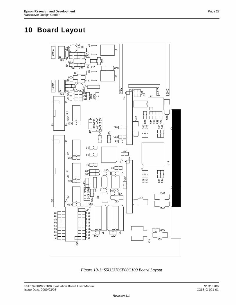
10 Board Layout
Figure 10-1: S5U13706P00C100 Board Layout
S5U13706P00C100 Evaluation Board User Manual S1D13706Issue Date: 2009/03/03 X31B-G-021-01
Revision 1.1

Page 28 Epson Research and DevelopmentVancouver Design Center
11 Technical Support
11.1 EPSON LCD Controllers (S1D13706)
AMERICA EPSON ELECTRONICS AMERICA, INC. 2580 Orchard Parkway San Jose, CA 95131,USA Phone: +1-800-228-3964 FAX: +1-408-922-0238
EUROPEEPSON EUROPE ELECTRONICS GmbH Riesstrasse 15, 80992 Munich,GERMANY Phone: +49-89-14005-0 FAX: +49-89-14005-110
ASIA EPSON (CHINA) CO., LTD.7F, Jinbao Bldg., No.89 Jinbao St.,
Beijing 100005, CHINAPhone: +86-10-6410-6655 FAX: +86-10-6410-7320
SHANGHAI BRANCH7F, Block B, High-Tech Bldg., 900, Yishan Road, Shanghai 200233, CHINA Phone: +86-21-5423-5522 FAX: +86-21-5423-5512
EPSON HONG KONG LTD.20/F, Harbour Centre, 25 Harbour Road Wanchai, Hong Kong Phone: +852-2585-4600 FAX: +852-2827-4346 Telex: 65542 EPSCO HX
SHENZHEN BRANCH12F, Dawning Mansion, Keji South 12th Road,Hi-Tech Park, Shenzhen 518057, CHINAPhone: +86-755-2699-3828 FAX: +86-755-2699-3838
EPSON TAIWAN TECHNOLOGY & TRADING LTD.14F, No. 7, Song Ren Road, Taipei 110, TAIWANPhone: +886-2-8786-6688 FAX: +886-2-8786-6660
EPSON SINGAPORE PTE., LTD.1 HarbourFront Place, #03-02 HarbourFront Tower One, Singapore 098633 Phone: +65-6586-5500 FAX: +65-6271-3182
SEIKO EPSON CORP. KOREA OFFICE 50F, KLI 63 Bldg., 60 Yoido-dong Youngdeungpo-Ku, Seoul, 150-763, KOREA Phone: +82-2-784-6027 FAX: +82-2-767-3677
SEIKO EPSON CORP. SEMICONDUCTOR OPERATIONS DIVISION
IC Sales Dept.IC International Sales Group 421-8, Hino, Hino-shi, Tokyo 191-8501, JAPAN Phone: +81-42-587-5814 FAX: +81-42-587-5117
Dongcheng District,
S1D13706 S5U13706P00C100 Evaluation Board User ManualX31B-G-021-01 Issue Date: 2009/03/03
Revision 1.1

Epson Research and Development Page 29Vancouver Design Center
Change Record
X31B-G-021-01 Revision 1.1 - Issued: March 03, 2009
• section 11 - update sales office addresses
X31B-G-021-01 Revision 1.0 - Issued: March 19, 2007
• initial draft
• minor edits
• added parts list
• added schematics
• updated tech support contact information
S5U13706P00C100 Evaluation Board User Manual S1D13706Issue Date: 2009/03/03 X31B-G-021-01
Revision 1.1